WO2014136149A1 - El表示装置 - Google Patents
El表示装置 Download PDFInfo
- Publication number
- WO2014136149A1 WO2014136149A1 PCT/JP2013/004907 JP2013004907W WO2014136149A1 WO 2014136149 A1 WO2014136149 A1 WO 2014136149A1 JP 2013004907 W JP2013004907 W JP 2013004907W WO 2014136149 A1 WO2014136149 A1 WO 2014136149A1
- Authority
- WO
- WIPO (PCT)
- Prior art keywords
- pixels
- subpixels
- light
- bank
- light emitting
- Prior art date
- Legal status (The legal status is an assumption and is not a legal conclusion. Google has not performed a legal analysis and makes no representation as to the accuracy of the status listed.)
- Ceased
Links
Images




Classifications
-
- H—ELECTRICITY
- H10—SEMICONDUCTOR DEVICES; ELECTRIC SOLID-STATE DEVICES NOT OTHERWISE PROVIDED FOR
- H10K—ORGANIC ELECTRIC SOLID-STATE DEVICES
- H10K59/00—Integrated devices, or assemblies of multiple devices, comprising at least one organic light-emitting element covered by group H10K50/00
- H10K59/30—Devices specially adapted for multicolour light emission
- H10K59/35—Devices specially adapted for multicolour light emission comprising red-green-blue [RGB] subpixels
- H10K59/352—Devices specially adapted for multicolour light emission comprising red-green-blue [RGB] subpixels the areas of the RGB subpixels being different
-
- H—ELECTRICITY
- H10—SEMICONDUCTOR DEVICES; ELECTRIC SOLID-STATE DEVICES NOT OTHERWISE PROVIDED FOR
- H10K—ORGANIC ELECTRIC SOLID-STATE DEVICES
- H10K59/00—Integrated devices, or assemblies of multiple devices, comprising at least one organic light-emitting element covered by group H10K50/00
- H10K59/10—OLED displays
- H10K59/12—Active-matrix OLED [AMOLED] displays
- H10K59/122—Pixel-defining structures or layers, e.g. banks
-
- H—ELECTRICITY
- H10—SEMICONDUCTOR DEVICES; ELECTRIC SOLID-STATE DEVICES NOT OTHERWISE PROVIDED FOR
- H10K—ORGANIC ELECTRIC SOLID-STATE DEVICES
- H10K59/00—Integrated devices, or assemblies of multiple devices, comprising at least one organic light-emitting element covered by group H10K50/00
- H10K59/30—Devices specially adapted for multicolour light emission
- H10K59/35—Devices specially adapted for multicolour light emission comprising red-green-blue [RGB] subpixels
- H10K59/353—Devices specially adapted for multicolour light emission comprising red-green-blue [RGB] subpixels characterised by the geometrical arrangement of the RGB subpixels
Definitions
- This technology relates to an EL display device.
- EL Electrode
- a first electrode, a plurality of organic layers including a light emitting layer, and a second electrode are sequentially stacked on a driving substrate.
- the EL display device is a self-luminous type, it has a wide viewing angle and does not require a backlight, so that it can be expected to save power, has high responsiveness, and can reduce the thickness of the device. Therefore, application to a large screen display device such as a television is strongly desired.
- an organic EL light emitting element it is necessary to form an organic EL light emitting portion in three colors of red, blue, and green and four colors such as red, blue, green, and white for each pixel.
- the most common method is a method of forming an organic EL portion by vapor deposition only on the hole using a fine metal mask with fine holes.
- an organic EL part that develops red color with a red fine metal mask is formed by vapor deposition
- an organic EL part that produces green color with a fine metal mask for green is formed by vapor deposition
- a blue color is produced with a blue fine metal mask.
- An organic EL part is formed by vapor deposition to form red, green, and blue light emitting parts.
- the first method is a method in which a white organic EL element is formed over the entire display area and colored and displayed by four color filters of red, green, blue and white. This method is effective in forming a large screen or creating a high-definition display.
- Another method is a method of forming an organic EL light emitting portion by a coating method.
- Various application methods have been studied as the coating method, and broadly divided into those using letterpress printing, flexographic printing, screen printing, and gravure printing, and those using the ink jet method (see Patent Document 1).
- one pixel is configured by subpixels that emit light of at least red, green, and blue emission colors, and a light emitting unit in which a plurality of pixels are arranged and a light emission of the light emitting unit are controlled.
- a thin film transistor array device Each sub-pixel of the pixel is configured by disposing at least red, green, and blue light-emitting layers in regions partitioned by banks.
- Subpixels of the same color formed in adjacent pixels are configured by disposing a light emitting layer in a combined bank having an area where banks for at least two subpixels are combined.
- an EL display device that uses an ink jet method suitable for manufacturing a large-screen EL display device, suppresses variation in light emission efficiency of each subpixel, and can achieve high definition.
- FIG. 1 is a perspective view of an organic EL display device according to an embodiment of the present technology.
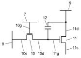
- FIG. 2 is an electric circuit diagram showing a circuit configuration of the pixel circuit.
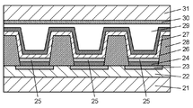
- FIG. 3 is a cross-sectional view showing a cross-sectional structure of an RGB pixel portion in an EL display device.
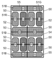
- FIG. 4 is an explanatory diagram showing an arrangement configuration of sub-pixels constituting a pixel in an EL display device according to an embodiment of the present technology.
- FIG. 5 is an explanatory diagram showing an arrangement configuration of sub-pixels constituting a pixel in an EL display device according to another embodiment of the present technology.
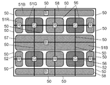
- FIG. 6 is an explanatory diagram showing an arrangement configuration of sub-pixels constituting a pixel in an EL display device according to another embodiment of the present technology.
- FIG. 7 is an explanatory diagram showing an arrangement configuration of sub-pixels constituting a pixel in an EL display device according to another embodiment of the present technology.
- FIG. 8 is an explanatory diagram showing an arrangement configuration of sub-pixels constituting a pixel in an EL display device according to another embodiment of the present technology.
- FIG. 1 is a perspective view showing a schematic configuration of an EL display device
- FIG. 2 is a diagram showing a circuit configuration of a pixel circuit for driving a pixel.
- the EL display device includes a thin film transistor array device 1 in which a plurality of thin film transistors are arranged, an anode 2 as a lower electrode, a light emitting layer 3 made of an organic material, and a cathode as a transparent upper electrode. 4 and the light emitting part.
- the light emitting unit is controlled to emit light by the thin film transistor array device 1.
- the light emitting unit has a configuration in which the light emitting layer 3 is disposed between the anode 2 and the cathode 4 which are a pair of electrodes.
- a hole transport layer is laminated between the anode 2 and the light emitting layer 3, and an electron transport layer is laminated between the light emitting layer 3 and the transparent cathode 4.
- the thin film transistor array device 1 has a plurality of pixels 5 arranged in a matrix.
- the thin film transistor array device 1 includes a plurality of gate wirings 7 arranged in a row, a plurality of signal wirings 8 arranged in a row so as to cross the gate wirings 7, and a parallel to the source wiring 8. And a plurality of power supply wires 9 (not shown in FIG. 1).
- the gate wiring 7 is connected to the gate electrode 10g of the thin film transistor 10 operating as a switching element included in each of the pixel circuits 6 for each row.
- the source line 8 is connected to the source electrode 10 s of the thin film transistor 10 that operates as a switching element included in each pixel circuit 6 for each column.
- the power supply wiring 9 is connected to the drain electrode 11d of the thin film transistor 11 that operates as a driving element included in each of the pixel circuits 6 for each column.
- the pixel circuit 6 includes a thin film transistor 10 that operates as a switching element, a thin film transistor 11 that operates as a driving element, and a capacitor 12 that stores data to be displayed in the corresponding pixel.
- the thin film transistor 10 includes a gate electrode 10g connected to the gate wiring 7, a source electrode 10s connected to the source wiring 8, a drain electrode 10d connected to the gate electrode 11g of the capacitor 12 and the thin film transistor 11, and a semiconductor film (FIG. Not shown).
- the thin film transistor 10 stores the voltage value applied to the source wiring 8 in the capacitor 12 as display data.
- the thin film transistor 11 includes a gate electrode 11g connected to the drain electrode 10d of the thin film transistor 10, a drain electrode 11d connected to the power supply wiring 9 and the capacitor 12, a source electrode 11s connected to the anode 2, and a semiconductor film (not shown). Z).
- the thin film transistor 11 supplies a current corresponding to the voltage value held by the capacitor 12 from the power supply wiring 9 to the anode 2 through the source electrode 11s. That is, the EL display device having the above configuration employs an active matrix system in which display control is performed for each pixel 5 located at the intersection of the gate line 7 and the source line 8.
- the light-emitting portion that emits at least red, green, and blue light-emitting colors has a matrix of a plurality of sub-pixels having at least red (R), green (G), and blue (B) light-emitting layers.
- a plurality of pixels are formed in an array.
- the sub-pixels constituting each pixel are separated from each other by a bank.
- This bank is provided by forming a ridge extending in parallel with the gate wiring 7 and a ridge extending in parallel with the source wiring 8 so as to intersect each other.
- a subpixel having an RGB light emitting layer is formed in a portion surrounded by the protrusions, that is, an opening of the bank.
- FIG. 3 is a cross-sectional view showing the cross-sectional structure of the RGB sub-pixel portion in the EL display device.
- a thin film transistor array device 22 constituting the pixel circuit 6 described above is formed on a base substrate 21 such as a glass substrate or a flexible resin substrate.
- an anode 23 which is a lower electrode, is formed through a planarization insulating film (not shown).
- a hole transport layer 24, an RGB light emitting layer 25 made of an organic material, an electron transport layer 26, and a cathode 27, which is a transparent upper electrode, are sequentially stacked.
- An EL light emitting unit is configured.
- the light emitting layer 25 of the light emitting part is formed in a region partitioned by the bank 28 which is an insulating layer.
- the bank 28 is for ensuring insulation between the anode 23 and the cathode 27 and partitioning the light emitting region into a predetermined shape, and is made of, for example, a photosensitive resin such as silicon oxide or polyimide.
- the hole transport layer 24 and the electron transport layer 26 are shown, but the hole transport layer 24 and the electron transport layer 26 are laminated with a hole injection layer and an electron injection layer, respectively. Is formed.
- the light emitting portion configured in this manner is covered with a sealing layer 29 such as silicon nitride, and further, a sealing substrate such as a transparent glass substrate or flexible resin substrate via an adhesive layer 30 on the sealing layer 29. 31 is sealed by being bonded over the entire surface.
- a sealing layer 29 such as silicon nitride
- a sealing substrate such as a transparent glass substrate or flexible resin substrate via an adhesive layer 30 on the sealing layer 29. 31 is sealed by being bonded over the entire surface.
- the shape, material, size and the like of the base substrate 21 are not particularly limited, and can be appropriately selected according to the purpose.
- a glass material such as alkali-free glass or soda glass, a silicon substrate, or a metal substrate may be used.
- Polyethylene terephthalate, polycarbonate, polyethylene naphthalate, polyamide, polyimide, etc. are suitable as the polymer material, but other known polymers such as acetate resin, acrylic resin, polyethylene, polypropylene, polyvinyl chloride resin, etc.
- a substrate material may be used.
- an organic EL light emitting element is formed after forming a polymer substrate on a rigid base material such as glass by a coating method or pasting, and then a rigid material such as glass is formed.
- a manufacturing method is used to remove a substrate.
- the anode 23 is a metal material having good electrical conductivity such as aluminum, aluminum alloy or copper, or a metal oxide or metal sulfide having high electrical conductivity such as light-transmitting IZO, ITO, tin oxide, indium oxide or zinc oxide. Etc.
- a thin film forming method such as a vacuum deposition method, a sputtering method, or an ion plating method is used.
- a polyvinyl carbazole material, a polysilane material, a polysiloxane derivative, a phthalocyanine compound such as copper phthalocyanine, an aromatic amine compound, or the like is used.
- a film forming method various coating methods can be used, and the film is formed to a thickness of about 10 nm to 200 nm.
- the hole injection layer stacked on the hole transport layer 24 is a layer that enhances hole injection from the anode 23, and is a metal oxide such as molybdenum oxide, vanadium oxide, or aluminum oxide, metal nitride, or metal oxide. Nitride is formed by sputtering.
- the light emitting layer 25 is mainly composed of an organic material that emits fluorescence, phosphorescence, and the like, and a dopant is added as necessary to improve the characteristics.
- a dopant is added as necessary to improve the characteristics.
- a high molecular weight organic material suitable for the printing method a polyvinyl carbazole derivative, a polyparaphenylin derivative, a polyfluorene derivative, a polyphenylene vinylene derivative, or the like is used.
- the dopant is used for shifting the emission wavelength and improving the light emission efficiency, and many dye-based and metal complex-based dopants have been developed.
- a printing method is suitable. Among various printing methods, an ink jet method is used, and the light emitting layer 25 having a thickness of about 20 nm to 200 nm is formed.
- the electron transport layer 26 is made of a material such as a benzoquinone derivative, a polyquinoline derivative, or an oxadiazole derivative.
- a film forming method a vacuum deposition method or a coating method is used, and the film is usually formed to a thickness of about 10 nm to 200 nm.
- the electron injection layer is made of a material such as barium, phthalocyanine, or lithium fluoride, and is formed by a vacuum deposition method or a coating method.
- the material of the cathode 27 differs depending on the light extraction direction.
- a light-transmitting conductive material such as ITO, IZO, tin oxide, or zinc oxide is used.
- materials such as platinum, gold, silver, copper, tungsten, aluminum, and aluminum alloy are used.
- a film forming method a sputtering method or a vacuum evaporation method is used, and the film is formed to a thickness of about 50 nm to 500 nm.
- the bank 28 is a structure necessary for filling a sufficient amount of a solution containing the material of the light emitting layer 25 in the region, and is formed in a predetermined shape by a photolithography method.
- the shape of the sub-pixels of the organic EL light emitting unit can be controlled by the shape of the bank 28.
- FIG. 4 is an explanatory diagram showing an arrangement configuration of RGB sub-pixels constituting a pixel in the EL display device according to the embodiment of the present technology.
- FIG. 4 is a diagram illustrating an example in which eight pixels 50 of 2 ⁇ 4 are arranged.
- Each pixel 50 includes four subpixels 51R, 51G, and 51B for RGB and subpixels 51b for light blue (b). Of sub-pixels.
- the light emitting layers of the subpixels 51R, 51G, 51B, and 51b constituting the adjacent pixels 50 have a rectangular shape with an area obtained by combining banks of two subpixels.
- One combination bank 52 is formed. That is, the first combination bank 52 has an area corresponding to two subpixels.
- a plurality of pixels are formed on the entire surface of the panel by combining subpixels 51R, 51G, 51B, and 51b each having a light emitting layer formed in the first coupling bank 52. Note that the light emitting layers of some of the subpixels 51G and 51B constituting the upper and lower pixels 50 of the panel are formed in the individual bank 53 for one subpixel.
- an EL display device that forms a light-emitting layer using an inkjet method, which is a printing method
- the pixel size is reduced due to high definition, the size of RGB subpixels is also reduced, so the light-emitting layer is formed in the bank with high accuracy. This makes it difficult to spill the solution of the light emitting material forming the light emitting layer into adjacent banks, and color mixing occurs between subpixels.
- the light emitting layers of the subpixels 51R, 51G, 51B, and 51b constituting the adjacent pixels 50 are formed in the rectangular first coupling bank 52 having an area corresponding to two subpixels. Therefore, by using the first coupling bank 52, the problem that the solution of the light emitting material forming the light emitting layer is spilled into the adjacent bank can be reduced, and color mixing between subpixels can be prevented. it can.
- FIG. 5 is an explanatory diagram showing another example of an arrangement configuration of RGB sub-pixels constituting a pixel in the EL display device according to the present technology.
- FIG. 5 is a diagram illustrating an example in which eight pixels 50 of 2 ⁇ 4 are arranged, and each pixel 50 includes three subpixels of RGB subpixels 51R, 51G, and 51B.
- the light emitting layers of the subpixels 51R and 51G constituting the pixels 50 adjacent in the vertical direction are formed in a rectangular first combination bank 52 having an area obtained by combining banks for two subpixels.
- the light emitting layer of the B sub-pixel 51B is formed in a second combination bank 54 having an area obtained by combining banks of eight sub-pixels constituting the pixels 50 adjacent in the vertical direction and the horizontal direction. Note that the light-emitting layer of the B sub-pixel 51B that constitutes the upper and lower pixels 50 of the panel is in the third combination bank 55 having an area in which banks of four sub-pixels of the pixel 50 adjacent in the horizontal direction are combined. Is formed.
- FIG. 6 is an explanatory diagram showing another example of an arrangement configuration of RGB sub-pixels constituting a pixel in an EL display device according to the present technology.
- FIG. 6 is a diagram illustrating an example in which 16 pixels 50 of 4 ⁇ 4 are arranged, and each pixel 50 includes four subpixels of RGB and white (W) subpixels 51R, 51G, 51B, and 51W. It is comprised by. Further, the light emitting layers of the subpixels 51R, 51G, 51B, and 51W constituting the adjacent pixels 50 are formed in the fourth combination bank 56 having an area obtained by combining the banks for the four subpixels.
- the pixels 50 at the upper, lower, left and right ends of the panel are formed in a rectangular first combination bank 52 having an area in which banks for two subpixels are combined in the vertical direction or the horizontal direction.
- the corner pixel 50 is formed in an individual bank 53 having an area corresponding to one subpixel.
- FIG. 7 is an explanatory diagram showing another example of an arrangement configuration of RGB sub-pixels constituting a pixel in the EL display device according to the present technology.
- FIG. 7 is a diagram illustrating an example in which 16 pixels 50 of 4 ⁇ 4 are arranged.
- each pixel 50 does not use the W subpixel 51 ⁇ / b> W, and the RGB subpixels 51 ⁇ / b> R, 51 ⁇ / b> G, It is composed of three subpixels 51B.
- the light emitting layers of the subpixels 51R and 51G constituting the adjacent pixels 50 are formed in the fourth combined bank 56 having an area obtained by combining the banks for the four subpixels, and the light emitting layer of the subpixel 51B is A fourth combined bank 56 having an area where banks for four subpixels are combined is formed in a fifth combined bank 57 having an area combined in the lateral direction.
- the sub-pixel 51R or sub-pixel 51G (sub-pixel 51R in FIG. 7) has a rectangular shape with an area in which banks for two sub-pixels are combined in the vertical direction.
- a light emitting layer is formed in the first coupling bank 52, and the subpixel 51B has a light emitting layer in the rectangular sixth coupling bank 58 having an area obtained by combining banks of eight subpixels in the horizontal direction. Is formed.
- FIG. 8 is an explanatory diagram showing another example of an arrangement configuration of RGB sub-pixels constituting a pixel in an EL display device according to the present technology.
- each pixel 50 uses white (W) subpixels 51W instead of light blue (b) subpixels 51b, and RGB subpixels 51R, 51G, and 51B.
- the example comprised by four subpixels of the subpixel 51W is shown.
- bus electrodes 60 for electrically connecting the regions are wired between specific pixels 50 or within the pixels 50. .
- the configuration of the bank is the same as the example shown in FIG.
- the light emitting layers of the subpixels 51R, 51G, 51B, 51b, and 51W constituting the adjacent pixels 50 are two to It is formed in the first combination bank 52 and the second combination bank 54 to the sixth combination bank 58 having a rectangular shape with an area where banks of 16 subpixels are combined.
- the horizontal width is about 57 ⁇ m
- the vertical direction is about 121 ⁇ m, which is more than twice the horizontal direction, and a light emitting layer is formed by an ink jet method. In this case, it is possible to separate the colors without causing color mixing.
- the shape of the bank is increased, the number of droplets of the luminescent material solution discharged into the bank can be increased.
- the variation in the amount of droplets can be reduced compared to the case where the number of droplets is small, the variation in the thickness of the light emitting layer due to the variation in the amount of droplets can be reduced, and the variation in the light emission characteristics can also be reduced. it can.
- the subpixels of the same color formed in the adjacent pixels have the light emitting layer disposed in the coupling bank having an area corresponding to at least two subpixels. It is constituted by.
- the top emission type which is a structure that can easily achieve higher definition, is used.
- the present technology is also effective for a bottom emission structure.
- the subpixels of the same color formed in adjacent pixels may be configured by arranging a light emitting layer having an area corresponding to at least two subpixels. The present invention can also be applied to an EL display device having the same.
- the present invention is useful for easily realizing high definition EL display devices.
Landscapes
- Engineering & Computer Science (AREA)
- Microelectronics & Electronic Packaging (AREA)
- Electroluminescent Light Sources (AREA)
- Devices For Indicating Variable Information By Combining Individual Elements (AREA)
Abstract
Description
2 陽極
3 発光層
4 陰極
5 画素
6 画素回路
7 ゲート配線
8 ソース配線
9 電源配線
10,11 薄膜トランジスタ
21 ベース基板
22 薄膜トランジスタアレイ装置
23 陽極
24 正孔輸送層
25 発光層
26 電子輸送層
27 陰極
28 バンク
29 封止層
30 接着層
31 封止用基板
50 画素
51R,51G,51B,51b,51W サブピクセル
52 第1の結合バンク
53 個別バンク
54 第2の結合バンク
55 第3の結合バンク
56 第4の結合バンク
57 第5の結合バンク
58 第6の結合バンク
Claims (5)
- 1画素が少なくとも赤色、緑色および青色の発光色で発光するサブピクセルにより構成され、複数個の画素を配列して配置した発光部と、前記発光部の発光を制御する薄膜トランジスタアレイ装置とを備え、
隣接する画素に形成される同一色のサブピクセルは、少なくとも2個のサブピクセルに対応する面積の発光層を配置することにより構成されていることを特徴とするEL表示装置。 - 1画素が少なくとも赤色、緑色および青色の発光色で発光するサブピクセルにより構成され、複数個の画素を配列して配置した発光部と、前記発光部の発光を制御する薄膜トランジスタアレイ装置とを備え、
前記画素の各サブピクセルは、バンクにより格子状に区画された領域に少なくとも赤色、緑色および青色の発光層を配置することにより構成され、
隣接する画素に形成される同一色のサブピクセルは、少なくとも2個のサブピクセル分のバンクを結合させた面積の結合バンク内に発光層を配置することにより構成されていることを特徴とするEL表示装置。 - 縦方向に隣接する画素を構成する赤色、緑色のサブピクセルの発光層は、2個のサブピクセル分のバンクを結合させた面積の長方形状の第1の結合バンク内に形成され、
青色のサブピクセルの発光層は、縦方向および横方向に隣接する画素を構成する8個のサブピクセル分のバンクを結合させた面積の第2の結合バンク内に形成されていることを特徴とする請求項2に記載のEL表示装置。 - 隣接する画素を構成するサブピクセルの発光層は、4個のサブピクセル分のバンクを結合させた面積の第4の結合バンクに形成されていることを特徴とする請求項2に記載のEL表示装置。
- 隣接する画素を構成するサブピクセルの発光層は、4個のサブピクセル分のバンクを結合させた面積の第4の結合バンクに形成され、
青色のサブピクセルの発光層は、4個のサブピクセル分のバンクを結合させた面積の第4の結合バンクを、さらに横方向において結合させた面積の第5の結合バンクに形成されていることを特徴とする請求項2に記載のEL表示装置。
Priority Applications (2)
| Application Number | Priority Date | Filing Date | Title |
|---|---|---|---|
| US14/772,103 US20160013251A1 (en) | 2013-03-04 | 2013-08-20 | El display device |
| JP2015504001A JPWO2014136149A1 (ja) | 2013-03-04 | 2013-08-20 | El表示装置 |
Applications Claiming Priority (2)
| Application Number | Priority Date | Filing Date | Title |
|---|---|---|---|
| JP2013041516 | 2013-03-04 | ||
| JP2013-041516 | 2013-03-04 |
Publications (1)
| Publication Number | Publication Date |
|---|---|
| WO2014136149A1 true WO2014136149A1 (ja) | 2014-09-12 |
Family
ID=51490718
Family Applications (1)
| Application Number | Title | Priority Date | Filing Date |
|---|---|---|---|
| PCT/JP2013/004907 Ceased WO2014136149A1 (ja) | 2013-03-04 | 2013-08-20 | El表示装置 |
Country Status (3)
| Country | Link |
|---|---|
| US (1) | US20160013251A1 (ja) |
| JP (1) | JPWO2014136149A1 (ja) |
| WO (1) | WO2014136149A1 (ja) |
Cited By (16)
| Publication number | Priority date | Publication date | Assignee | Title |
|---|---|---|---|---|
| CN104992945A (zh) * | 2015-05-28 | 2015-10-21 | 京东方科技集团股份有限公司 | 显示基板及其制作方法以及显示装置 |
| JP2016090595A (ja) * | 2014-10-29 | 2016-05-23 | 株式会社ジャパンディスプレイ | 表示装置 |
| CN105826348A (zh) * | 2015-01-05 | 2016-08-03 | 上海和辉光电有限公司 | Oled显示面板的像素排列结构 |
| CN106449710A (zh) * | 2016-10-31 | 2017-02-22 | 昆山工研院新型平板显示技术中心有限公司 | 像素结构以及包含该像素结构的oled显示面板 |
| JP6329711B1 (ja) * | 2017-07-05 | 2018-05-23 | 堺ディスプレイプロダクト株式会社 | 有機el表示装置および有機el表示装置の製造方法 |
| KR20180076820A (ko) * | 2016-12-28 | 2018-07-06 | 엘지디스플레이 주식회사 | 전계 발광 표시 장치 |
| WO2018223475A1 (zh) * | 2017-06-09 | 2018-12-13 | 深圳市华星光电技术有限公司 | Oled显示面板的像素排列结构及oled显示面板 |
| JP2021513089A (ja) * | 2018-02-09 | 2021-05-20 | 京東方科技集團股▲ふん▼有限公司Boe Technology Group Co.,Ltd. | 画素配列構造及びその表示方法と製造方法、並びに表示基板 |
| CN115171543A (zh) * | 2022-06-27 | 2022-10-11 | 湖北长江新型显示产业创新中心有限公司 | 显示面板及拼接显示装置 |
| US11574960B2 (en) | 2018-02-09 | 2023-02-07 | Boe Technology Group Co., Ltd. | Pixel arrangement structure, display substrate, display device and mask plate group |
| US11735108B2 (en) | 2019-07-31 | 2023-08-22 | Boe Technology Group Co., Ltd. | Display substrate and preparation method thereof, display panel, and display device |
| US11747531B2 (en) | 2016-02-18 | 2023-09-05 | Chengdu Boe Optoelectronics Technology Co., Ltd. | Display substrate, fine metal mask set and manufacturing method thereof |
| WO2023209494A1 (ja) * | 2022-04-29 | 2023-11-02 | 株式会社半導体エネルギー研究所 | 表示装置、表示モジュール、電子機器 |
| US12058910B2 (en) | 2016-02-18 | 2024-08-06 | Boe Technology Group Co., Ltd. | Pixel arrangement structure and driving method thereof, display substrate and display device |
| US12310182B2 (en) | 2019-07-31 | 2025-05-20 | Boe Technology Group Co., Ltd. | Display substrate and display device with spacers |
| US12369477B2 (en) | 2018-02-09 | 2025-07-22 | Boe Technology Group Co., Ltd. | Pixel arrangement structure, display substrate, and display device |
Families Citing this family (10)
| Publication number | Priority date | Publication date | Assignee | Title |
|---|---|---|---|---|
| JP2016081562A (ja) * | 2014-10-09 | 2016-05-16 | ソニー株式会社 | 表示装置、表示装置の製造方法および電子機器 |
| KR102930671B1 (ko) * | 2016-12-14 | 2026-02-24 | 엘지디스플레이 주식회사 | 유기 발광 표시 장치 |
| US10937836B2 (en) * | 2018-09-13 | 2021-03-02 | Wuhan China Star Optoelectronics Semiconductor Display Technology Co., Ltd. | Pixel arrangement structure and display device |
| US11211430B2 (en) * | 2019-01-28 | 2021-12-28 | Chengdu Boe Optoelectronics Technology Co., Ltd. | Display panel for improving display effect in low-resolution area, manufacturing method thereof, and display device |
| CN109920833B (zh) * | 2019-03-27 | 2020-11-03 | 京东方科技集团股份有限公司 | 一种阵列基板及其制备方法、显示面板、显示装置 |
| KR102704022B1 (ko) * | 2019-09-23 | 2024-09-05 | 엘지디스플레이 주식회사 | 표시장치 및 이의 제조방법 |
| KR20220064479A (ko) * | 2020-11-11 | 2022-05-19 | 삼성디스플레이 주식회사 | 디스플레이 패널 및 이를 구비하는 디스플레이 장치 |
| CN112599585A (zh) * | 2020-12-30 | 2021-04-02 | 深圳市华星光电半导体显示技术有限公司 | 显示面板、显示母板及显示装置 |
| CN112712762B (zh) | 2020-12-30 | 2022-05-03 | 深圳市华星光电半导体显示技术有限公司 | 显示面板、显示母板及显示装置 |
| CN113675247B (zh) * | 2021-07-29 | 2022-01-07 | 北京京东方技术开发有限公司 | 显示面板、显示面板的制造方法和显示装置 |
Citations (5)
| Publication number | Priority date | Publication date | Assignee | Title |
|---|---|---|---|---|
| JP2004207126A (ja) * | 2002-12-26 | 2004-07-22 | Denso Corp | 有機elパネル |
| JP2005203351A (ja) * | 2003-12-17 | 2005-07-28 | Semiconductor Energy Lab Co Ltd | 表示装置及びその作製方法 |
| JP2009069323A (ja) * | 2007-09-12 | 2009-04-02 | Canon Inc | 画素表示装置 |
| JP2009187730A (ja) * | 2008-02-05 | 2009-08-20 | Seiko Epson Corp | 発光装置及び電子機器 |
| JP2009533810A (ja) * | 2006-04-12 | 2009-09-17 | ケンブリッジ ディスプレイ テクノロジー リミテッド | 光電子ディスプレイ及びその製造方法 |
-
2013
- 2013-08-20 US US14/772,103 patent/US20160013251A1/en not_active Abandoned
- 2013-08-20 WO PCT/JP2013/004907 patent/WO2014136149A1/ja not_active Ceased
- 2013-08-20 JP JP2015504001A patent/JPWO2014136149A1/ja active Pending
Patent Citations (5)
| Publication number | Priority date | Publication date | Assignee | Title |
|---|---|---|---|---|
| JP2004207126A (ja) * | 2002-12-26 | 2004-07-22 | Denso Corp | 有機elパネル |
| JP2005203351A (ja) * | 2003-12-17 | 2005-07-28 | Semiconductor Energy Lab Co Ltd | 表示装置及びその作製方法 |
| JP2009533810A (ja) * | 2006-04-12 | 2009-09-17 | ケンブリッジ ディスプレイ テクノロジー リミテッド | 光電子ディスプレイ及びその製造方法 |
| JP2009069323A (ja) * | 2007-09-12 | 2009-04-02 | Canon Inc | 画素表示装置 |
| JP2009187730A (ja) * | 2008-02-05 | 2009-08-20 | Seiko Epson Corp | 発光装置及び電子機器 |
Cited By (31)
| Publication number | Priority date | Publication date | Assignee | Title |
|---|---|---|---|---|
| JP2016090595A (ja) * | 2014-10-29 | 2016-05-23 | 株式会社ジャパンディスプレイ | 表示装置 |
| CN105826348A (zh) * | 2015-01-05 | 2016-08-03 | 上海和辉光电有限公司 | Oled显示面板的像素排列结构 |
| CN104992945A (zh) * | 2015-05-28 | 2015-10-21 | 京东方科技集团股份有限公司 | 显示基板及其制作方法以及显示装置 |
| US10026846B2 (en) | 2015-05-28 | 2018-07-17 | Boe Technology Group Co., Ltd. | Display substrate and fabrication method thereof and display device |
| US12058910B2 (en) | 2016-02-18 | 2024-08-06 | Boe Technology Group Co., Ltd. | Pixel arrangement structure and driving method thereof, display substrate and display device |
| US11747531B2 (en) | 2016-02-18 | 2023-09-05 | Chengdu Boe Optoelectronics Technology Co., Ltd. | Display substrate, fine metal mask set and manufacturing method thereof |
| US12196988B2 (en) | 2016-02-18 | 2025-01-14 | Chengdu Boe Optoelectronics Technology Co., Ltd. | Display substrate and display device |
| US12593588B2 (en) | 2016-02-18 | 2026-03-31 | Boe Technology Group Co., Ltd. | Display substrate |
| US12001035B2 (en) | 2016-02-18 | 2024-06-04 | Chengdu Boe Optoelectronics Technology Co., Ltd. | Display substrate and display device |
| CN106449710A (zh) * | 2016-10-31 | 2017-02-22 | 昆山工研院新型平板显示技术中心有限公司 | 像素结构以及包含该像素结构的oled显示面板 |
| CN106449710B (zh) * | 2016-10-31 | 2019-05-03 | 昆山工研院新型平板显示技术中心有限公司 | 像素结构以及包含该像素结构的oled显示面板 |
| KR102715998B1 (ko) | 2016-12-28 | 2024-10-10 | 엘지디스플레이 주식회사 | 전계 발광 표시 장치 |
| KR20180076820A (ko) * | 2016-12-28 | 2018-07-06 | 엘지디스플레이 주식회사 | 전계 발광 표시 장치 |
| WO2018223475A1 (zh) * | 2017-06-09 | 2018-12-13 | 深圳市华星光电技术有限公司 | Oled显示面板的像素排列结构及oled显示面板 |
| WO2019008705A1 (ja) * | 2017-07-05 | 2019-01-10 | 堺ディスプレイプロダクト株式会社 | 有機el表示装置および有機el表示装置の製造方法 |
| US11024677B2 (en) | 2017-07-05 | 2021-06-01 | Sakai Display Products Corporation | Organic EL display apparatus and method of manufacturing organic EL display apparatus |
| US10790338B2 (en) | 2017-07-05 | 2020-09-29 | Sakai Display Products Corporation | Organic EL display apparatus and method of manufacturing organic EL display apparatus |
| JP6329711B1 (ja) * | 2017-07-05 | 2018-05-23 | 堺ディスプレイプロダクト株式会社 | 有機el表示装置および有機el表示装置の製造方法 |
| US11574960B2 (en) | 2018-02-09 | 2023-02-07 | Boe Technology Group Co., Ltd. | Pixel arrangement structure, display substrate, display device and mask plate group |
| US11957019B2 (en) | 2018-02-09 | 2024-04-09 | Boe Technology Group Co., Ltd. | Pixel arrangement structure, display method and preparing method of pixel arrangement structure, and display substrate |
| US12035599B2 (en) | 2018-02-09 | 2024-07-09 | Boe Technology Group Co., Ltd. | Display substrate and display device |
| JP7264818B2 (ja) | 2018-02-09 | 2023-04-25 | 京東方科技集團股▲ふん▼有限公司 | 画素配列構造及びその表示方法と製造方法、並びに表示基板 |
| US12369477B2 (en) | 2018-02-09 | 2025-07-22 | Boe Technology Group Co., Ltd. | Pixel arrangement structure, display substrate, and display device |
| JP2021513089A (ja) * | 2018-02-09 | 2021-05-20 | 京東方科技集團股▲ふん▼有限公司Boe Technology Group Co.,Ltd. | 画素配列構造及びその表示方法と製造方法、並びに表示基板 |
| US11908410B2 (en) | 2019-07-31 | 2024-02-20 | Boe Technology Group Co., Ltd. | Display substrate and preparation method thereof, display panel, and display device |
| US11735108B2 (en) | 2019-07-31 | 2023-08-22 | Boe Technology Group Co., Ltd. | Display substrate and preparation method thereof, display panel, and display device |
| US12300179B2 (en) | 2019-07-31 | 2025-05-13 | Boe Technology Group Co., Ltd. | Display substrate and preparation method thereof, display panel, and display device |
| US12310182B2 (en) | 2019-07-31 | 2025-05-20 | Boe Technology Group Co., Ltd. | Display substrate and display device with spacers |
| WO2023209494A1 (ja) * | 2022-04-29 | 2023-11-02 | 株式会社半導体エネルギー研究所 | 表示装置、表示モジュール、電子機器 |
| CN115171543B (zh) * | 2022-06-27 | 2023-10-31 | 湖北长江新型显示产业创新中心有限公司 | 显示面板及拼接显示装置 |
| CN115171543A (zh) * | 2022-06-27 | 2022-10-11 | 湖北长江新型显示产业创新中心有限公司 | 显示面板及拼接显示装置 |
Also Published As
| Publication number | Publication date |
|---|---|
| US20160013251A1 (en) | 2016-01-14 |
| JPWO2014136149A1 (ja) | 2017-02-09 |
Similar Documents
| Publication | Publication Date | Title |
|---|---|---|
| JPWO2014136149A1 (ja) | El表示装置 | |
| CN103794631B (zh) | 柔性有机电致发光装置及其制造方法 | |
| KR101895616B1 (ko) | 유기 발광 표시 장치 및 그 제조 방법 | |
| KR20110111746A (ko) | 유기 발광 표시 장치 | |
| KR20160030009A (ko) | 고 개구율 유기발광 다이오드 표시장치 및 그 제조 방법 | |
| KR102035251B1 (ko) | 유기 발광 표시 장치 | |
| JP2018194572A (ja) | 表示装置 | |
| JP2011526719A (ja) | 発光装置 | |
| JP6111487B2 (ja) | El表示装置 | |
| KR20110023996A (ko) | 유기전계발광 표시장치 | |
| JP2015072761A (ja) | Oled表示装置 | |
| KR20150075188A (ko) | 유기전계발광표시장치 및 그 제조방법 | |
| KR102242982B1 (ko) | 유기전계 발광표시장치 및 그 제조방법 | |
| JPWO2014174803A1 (ja) | El表示装置の製造方法 | |
| KR101717075B1 (ko) | 유기전기발광소자 | |
| KR20170080756A (ko) | 보조전극 구조 및 이를 갖는 유기전계발광 표시 장치 | |
| WO2014174804A1 (ja) | El表示装置の製造方法 | |
| JP2007286212A (ja) | 有機el表示装置 | |
| WO2014174806A1 (ja) | El表示装置の製造方法 | |
| KR20100024033A (ko) | 유기발광 표시장치 및 그 제조방법 | |
| WO2015087461A1 (ja) | 表示装置 | |
| US11869421B2 (en) | Display device | |
| US12200985B2 (en) | Display device in which the occurrence of shading is reduced without excessively increasing the pixel spacing | |
| JPWO2014174805A1 (ja) | El表示装置の製造方法 | |
| KR102065108B1 (ko) | 유기 발광 표시 장치 |
Legal Events
| Date | Code | Title | Description |
|---|---|---|---|
| 121 | Ep: the epo has been informed by wipo that ep was designated in this application |
Ref document number: 13876932 Country of ref document: EP Kind code of ref document: A1 |
|
| ENP | Entry into the national phase |
Ref document number: 2015504001 Country of ref document: JP Kind code of ref document: A |
|
| WWE | Wipo information: entry into national phase |
Ref document number: 14772103 Country of ref document: US |
|
| NENP | Non-entry into the national phase |
Ref country code: DE |
|
| 122 | Ep: pct application non-entry in european phase |
Ref document number: 13876932 Country of ref document: EP Kind code of ref document: A1 |