WO2014125786A1 - 薄膜形成方法、及びそれを用いて作製した半導体基板ならびに電子デバイス - Google Patents
薄膜形成方法、及びそれを用いて作製した半導体基板ならびに電子デバイス Download PDFInfo
- Publication number
- WO2014125786A1 WO2014125786A1 PCT/JP2014/000560 JP2014000560W WO2014125786A1 WO 2014125786 A1 WO2014125786 A1 WO 2014125786A1 JP 2014000560 W JP2014000560 W JP 2014000560W WO 2014125786 A1 WO2014125786 A1 WO 2014125786A1
- Authority
- WO
- WIPO (PCT)
- Prior art keywords
- substrate
- thin film
- film
- silicon
- liquid
- Prior art date
- Legal status (The legal status is an assumption and is not a legal conclusion. Google has not performed a legal analysis and makes no representation as to the accuracy of the status listed.)
- Ceased
Links
Images














Classifications
-
- H—ELECTRICITY
- H10—SEMICONDUCTOR DEVICES; ELECTRIC SOLID-STATE DEVICES NOT OTHERWISE PROVIDED FOR
- H10D—INORGANIC ELECTRIC SEMICONDUCTOR DEVICES
- H10D30/00—Field-effect transistors [FET]
- H10D30/60—Insulated-gate field-effect transistors [IGFET]
- H10D30/67—Thin-film transistors [TFT]
- H10D30/6758—Thin-film transistors [TFT] characterised by the insulating substrates
-
- H—ELECTRICITY
- H10—SEMICONDUCTOR DEVICES; ELECTRIC SOLID-STATE DEVICES NOT OTHERWISE PROVIDED FOR
- H10D—INORGANIC ELECTRIC SEMICONDUCTOR DEVICES
- H10D30/00—Field-effect transistors [FET]
- H10D30/01—Manufacture or treatment
- H10D30/021—Manufacture or treatment of FETs having insulated gates [IGFET]
- H10D30/031—Manufacture or treatment of FETs having insulated gates [IGFET] of thin-film transistors [TFT]
- H10D30/0321—Manufacture or treatment of FETs having insulated gates [IGFET] of thin-film transistors [TFT] comprising silicon, e.g. amorphous silicon or polysilicon
- H10D30/0323—Manufacture or treatment of FETs having insulated gates [IGFET] of thin-film transistors [TFT] comprising silicon, e.g. amorphous silicon or polysilicon comprising monocrystalline silicon
-
- H—ELECTRICITY
- H10—SEMICONDUCTOR DEVICES; ELECTRIC SOLID-STATE DEVICES NOT OTHERWISE PROVIDED FOR
- H10D—INORGANIC ELECTRIC SEMICONDUCTOR DEVICES
- H10D30/00—Field-effect transistors [FET]
- H10D30/60—Insulated-gate field-effect transistors [IGFET]
- H10D30/67—Thin-film transistors [TFT]
- H10D30/6704—Thin-film transistors [TFT] having supplementary regions or layers in the thin films or in the insulated bulk substrates for controlling properties of the device
- H10D30/6713—Thin-film transistors [TFT] having supplementary regions or layers in the thin films or in the insulated bulk substrates for controlling properties of the device characterised by the properties of the source or drain regions, e.g. compositions or sectional shapes
-
- H—ELECTRICITY
- H10—SEMICONDUCTOR DEVICES; ELECTRIC SOLID-STATE DEVICES NOT OTHERWISE PROVIDED FOR
- H10D—INORGANIC ELECTRIC SEMICONDUCTOR DEVICES
- H10D30/00—Field-effect transistors [FET]
- H10D30/60—Insulated-gate field-effect transistors [IGFET]
- H10D30/67—Thin-film transistors [TFT]
- H10D30/674—Thin-film transistors [TFT] characterised by the active materials
- H10D30/6741—Group IV materials, e.g. germanium or silicon carbide
- H10D30/6743—Silicon
- H10D30/6744—Monocrystalline silicon
-
- H—ELECTRICITY
- H10—SEMICONDUCTOR DEVICES; ELECTRIC SOLID-STATE DEVICES NOT OTHERWISE PROVIDED FOR
- H10D—INORGANIC ELECTRIC SEMICONDUCTOR DEVICES
- H10D86/00—Integrated devices formed in or on insulating or conducting substrates, e.g. formed in silicon-on-insulator [SOI] substrates or on stainless steel or glass substrates
- H10D86/01—Manufacture or treatment
- H10D86/021—Manufacture or treatment of multiple TFTs
- H10D86/0214—Manufacture or treatment of multiple TFTs using temporary substrates
-
- H—ELECTRICITY
- H10—SEMICONDUCTOR DEVICES; ELECTRIC SOLID-STATE DEVICES NOT OTHERWISE PROVIDED FOR
- H10D—INORGANIC ELECTRIC SEMICONDUCTOR DEVICES
- H10D86/00—Integrated devices formed in or on insulating or conducting substrates, e.g. formed in silicon-on-insulator [SOI] substrates or on stainless steel or glass substrates
- H10D86/40—Integrated devices formed in or on insulating or conducting substrates, e.g. formed in silicon-on-insulator [SOI] substrates or on stainless steel or glass substrates characterised by multiple TFTs
- H10D86/421—Integrated devices formed in or on insulating or conducting substrates, e.g. formed in silicon-on-insulator [SOI] substrates or on stainless steel or glass substrates characterised by multiple TFTs having a particular composition, shape or crystalline structure of the active layer
-
- H—ELECTRICITY
- H10—SEMICONDUCTOR DEVICES; ELECTRIC SOLID-STATE DEVICES NOT OTHERWISE PROVIDED FOR
- H10D—INORGANIC ELECTRIC SEMICONDUCTOR DEVICES
- H10D86/00—Integrated devices formed in or on insulating or conducting substrates, e.g. formed in silicon-on-insulator [SOI] substrates or on stainless steel or glass substrates
- H10D86/40—Integrated devices formed in or on insulating or conducting substrates, e.g. formed in silicon-on-insulator [SOI] substrates or on stainless steel or glass substrates characterised by multiple TFTs
- H10D86/60—Integrated devices formed in or on insulating or conducting substrates, e.g. formed in silicon-on-insulator [SOI] substrates or on stainless steel or glass substrates characterised by multiple TFTs wherein the TFTs are in active matrices
-
- H—ELECTRICITY
- H10—SEMICONDUCTOR DEVICES; ELECTRIC SOLID-STATE DEVICES NOT OTHERWISE PROVIDED FOR
- H10F—INORGANIC SEMICONDUCTOR DEVICES SENSITIVE TO INFRARED RADIATION, LIGHT, ELECTROMAGNETIC RADIATION OF SHORTER WAVELENGTH OR CORPUSCULAR RADIATION
- H10F10/00—Individual photovoltaic cells, e.g. solar cells
- H10F10/10—Individual photovoltaic cells, e.g. solar cells having potential barriers
- H10F10/14—Photovoltaic cells having only PN homojunction potential barriers
-
- H—ELECTRICITY
- H10—SEMICONDUCTOR DEVICES; ELECTRIC SOLID-STATE DEVICES NOT OTHERWISE PROVIDED FOR
- H10F—INORGANIC SEMICONDUCTOR DEVICES SENSITIVE TO INFRARED RADIATION, LIGHT, ELECTROMAGNETIC RADIATION OF SHORTER WAVELENGTH OR CORPUSCULAR RADIATION
- H10F10/00—Individual photovoltaic cells, e.g. solar cells
- H10F10/10—Individual photovoltaic cells, e.g. solar cells having potential barriers
- H10F10/14—Photovoltaic cells having only PN homojunction potential barriers
- H10F10/146—Back-junction photovoltaic cells, e.g. having interdigitated base-emitter regions on the back side
-
- H—ELECTRICITY
- H10—SEMICONDUCTOR DEVICES; ELECTRIC SOLID-STATE DEVICES NOT OTHERWISE PROVIDED FOR
- H10F—INORGANIC SEMICONDUCTOR DEVICES SENSITIVE TO INFRARED RADIATION, LIGHT, ELECTROMAGNETIC RADIATION OF SHORTER WAVELENGTH OR CORPUSCULAR RADIATION
- H10F19/00—Integrated devices, or assemblies of multiple devices, comprising at least one photovoltaic cell covered by group H10F10/00, e.g. photovoltaic modules
- H10F19/30—Integrated devices, or assemblies of multiple devices, comprising at least one photovoltaic cell covered by group H10F10/00, e.g. photovoltaic modules comprising thin-film photovoltaic cells
-
- H—ELECTRICITY
- H10—SEMICONDUCTOR DEVICES; ELECTRIC SOLID-STATE DEVICES NOT OTHERWISE PROVIDED FOR
- H10F—INORGANIC SEMICONDUCTOR DEVICES SENSITIVE TO INFRARED RADIATION, LIGHT, ELECTROMAGNETIC RADIATION OF SHORTER WAVELENGTH OR CORPUSCULAR RADIATION
- H10F71/00—Manufacture or treatment of devices covered by this subclass
- H10F71/121—The active layers comprising only Group IV materials
-
- H—ELECTRICITY
- H10—SEMICONDUCTOR DEVICES; ELECTRIC SOLID-STATE DEVICES NOT OTHERWISE PROVIDED FOR
- H10F—INORGANIC SEMICONDUCTOR DEVICES SENSITIVE TO INFRARED RADIATION, LIGHT, ELECTROMAGNETIC RADIATION OF SHORTER WAVELENGTH OR CORPUSCULAR RADIATION
- H10F71/00—Manufacture or treatment of devices covered by this subclass
- H10F71/139—Manufacture or treatment of devices covered by this subclass using temporary substrates
-
- H—ELECTRICITY
- H10—SEMICONDUCTOR DEVICES; ELECTRIC SOLID-STATE DEVICES NOT OTHERWISE PROVIDED FOR
- H10F—INORGANIC SEMICONDUCTOR DEVICES SENSITIVE TO INFRARED RADIATION, LIGHT, ELECTROMAGNETIC RADIATION OF SHORTER WAVELENGTH OR CORPUSCULAR RADIATION
- H10F77/00—Constructional details of devices covered by this subclass
- H10F77/10—Semiconductor bodies
- H10F77/14—Shape of semiconductor bodies; Shapes, relative sizes or dispositions of semiconductor regions within semiconductor bodies
- H10F77/148—Shapes of potential barriers
-
- H—ELECTRICITY
- H10—SEMICONDUCTOR DEVICES; ELECTRIC SOLID-STATE DEVICES NOT OTHERWISE PROVIDED FOR
- H10P—GENERIC PROCESSES OR APPARATUS FOR THE MANUFACTURE OR TREATMENT OF DEVICES COVERED BY CLASS H10
- H10P90/00—Preparation of wafers not covered by a single main group of this subclass, e.g. wafer reinforcement
- H10P90/19—Preparing inhomogeneous wafers
- H10P90/1904—Preparing vertically inhomogeneous wafers
- H10P90/1906—Preparing SOI wafers
- H10P90/1914—Preparing SOI wafers using bonding
-
- H—ELECTRICITY
- H10—SEMICONDUCTOR DEVICES; ELECTRIC SOLID-STATE DEVICES NOT OTHERWISE PROVIDED FOR
- H10W—GENERIC PACKAGES, INTERCONNECTIONS, CONNECTORS OR OTHER CONSTRUCTIONAL DETAILS OF DEVICES COVERED BY CLASS H10
- H10W10/00—Isolation regions in semiconductor bodies between components of integrated devices
- H10W10/10—Isolation regions comprising dielectric materials
- H10W10/181—Semiconductor-on-insulator [SOI] isolation regions, e.g. buried oxide regions of SOI wafers
-
- Y—GENERAL TAGGING OF NEW TECHNOLOGICAL DEVELOPMENTS; GENERAL TAGGING OF CROSS-SECTIONAL TECHNOLOGIES SPANNING OVER SEVERAL SECTIONS OF THE IPC; TECHNICAL SUBJECTS COVERED BY FORMER USPC CROSS-REFERENCE ART COLLECTIONS [XRACs] AND DIGESTS
- Y02—TECHNOLOGIES OR APPLICATIONS FOR MITIGATION OR ADAPTATION AGAINST CLIMATE CHANGE
- Y02E—REDUCTION OF GREENHOUSE GAS [GHG] EMISSIONS, RELATED TO ENERGY GENERATION, TRANSMISSION OR DISTRIBUTION
- Y02E10/00—Energy generation through renewable energy sources
- Y02E10/50—Photovoltaic [PV] energy
- Y02E10/547—Monocrystalline silicon PV cells
-
- Y—GENERAL TAGGING OF NEW TECHNOLOGICAL DEVELOPMENTS; GENERAL TAGGING OF CROSS-SECTIONAL TECHNOLOGIES SPANNING OVER SEVERAL SECTIONS OF THE IPC; TECHNICAL SUBJECTS COVERED BY FORMER USPC CROSS-REFERENCE ART COLLECTIONS [XRACs] AND DIGESTS
- Y10—TECHNICAL SUBJECTS COVERED BY FORMER USPC
- Y10T—TECHNICAL SUBJECTS COVERED BY FORMER US CLASSIFICATION
- Y10T428/00—Stock material or miscellaneous articles
- Y10T428/24—Structurally defined web or sheet [e.g., overall dimension, etc.]
- Y10T428/24273—Structurally defined web or sheet [e.g., overall dimension, etc.] including aperture
- Y10T428/24322—Composite web or sheet
- Y10T428/24331—Composite web or sheet including nonapertured component
Definitions
- the present invention relates to a thin film forming method, and a semiconductor substrate and an electronic device manufactured using the method.
- the performance of thin film transistors and solar cells depends on the crystallinity of the silicon thin film formed on the quartz substrate, the glass substrate, and the flexible substrate. Therefore, conventionally, techniques for improving the crystallinity of a silicon thin film formed on a quartz substrate, a glass substrate, and a flexible substrate have been actively studied.
- Patent Document 1 As a typical method of forming a polycrystalline silicon film on a quartz substrate, a glass substrate, and a flexible substrate, a laser annealing method is known (Patent Document 1).
- High crystalline silicon films have been realized by improving the technology for forming silicon films on quartz, glass, and flexible substrates.
- Single crystal silicon films have been formed on quartz, glass, and flexible substrates. It is difficult to form.
- the present invention has been made in view of such problems, and its main purpose is to form a thin film such as a single crystal semiconductor film on a substrate such as a quartz substrate, a glass substrate, or a flexible substrate, and a method for forming the same.
- An object of the present invention is to provide a semiconductor substrate and an electronic device manufactured using the same.
- a thin film forming method includes a step of preparing a first substrate having a thin film formed on a surface thereof, a step of forming a plurality of openings in the thin film, and etching the first substrate through the openings. Forming a hollow portion between the first substrate and the thin film, interposing a liquid between the thin film and the second substrate, and attaching the thin film to the second substrate; Heating the first substrate and / or the second substrate, and in the heating step, the liquid interposed between the thin film and the second substrate is dried, so that the thin film is removed from the first substrate. It is separated and transferred to the second substrate.
- the thin film is formed on a first substrate with a sacrificial layer interposed therebetween, and the step of forming the hollow portion includes etching the sacrificial layer instead of the first substrate. In the heating step, the thin film is separated from the sacrificial layer and transferred to the second substrate.
- a semiconductor substrate according to an embodiment of the present invention is characterized by a semiconductor substrate including a semiconductor thin film transferred to the surface by the above-described thin film forming method.
- An electronic device is characterized by an electronic device having a semiconductor thin film transferred to a substrate surface by the above-described thin film forming method.
- a method of manufacturing a thin film transistor includes a step of preparing a first substrate having a semiconductor thin film formed on the surface with an insulating layer interposed therebetween, and the semiconductor thin film becomes a channel region and a source / drain region. Patterning the region, forming a plurality of openings in the semiconductor thin film to be the source / drain regions, and etching the insulating layer through the openings to form a hollow portion between the insulating layer and the semiconductor thin film.
- the channel region and the region to be the source / drain region are patterned in a matrix.
- a method for manufacturing a solar cell includes: a step of preparing a second substrate having a transparent electrode formed on a surface thereof; Including a step of sequentially transferring the first-conductivity-type semiconductor thin film and the second-conductivity-type semiconductor thin film. In the transfer step, a PN junction made of the semiconductor thin film is formed on the transparent electrode.
- a thin film forming method for forming a thin film such as a single crystal semiconductor film on a substrate such as a quartz substrate, a glass substrate, or a flexible substrate, and a semiconductor substrate and an electronic device manufactured using the thin film forming method are provided.
- a substrate such as a quartz substrate, a glass substrate, or a flexible substrate
- a semiconductor substrate and an electronic device manufactured using the thin film forming method are provided. Can do.
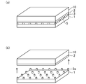
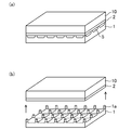
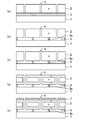
- (A)-(d) is process drawing which showed the thin film formation method in the 1st Embodiment of this invention.
- (A)-(b) is process drawing which showed the thin film formation method in the 1st Embodiment of this invention.
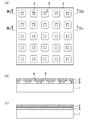
- (A)-(c) is the figure explaining the formation method of a hollow part.
- (A)-(c) is the figure explaining the formation method of a hollow part.
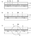
- (A)-(c) is the figure explaining the mechanism of transcription
- (A)-(c) is the figure explaining the mechanism of transcription
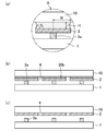
- (A)-(c) is process drawing which showed the heating method of the board
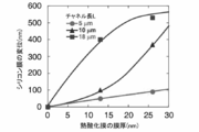
- FIG. 6 is a graph showing a relationship between a transfer rate and a liquid amount. It is the graph which showed the relationship between a transfer rate and heating temperature. It is the graph which showed the relationship between a transfer rate and pillar size.
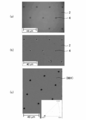
- (A) is an optical micrograph showing the surface of the thin film before transfer
- (b) is an SEM (scanning electron microscope) photo showing the surface of the thin film after transfer
- (c) is after transfer.
- 2 is an EBSD (electron beam backscatter diffraction) image of the thin film.
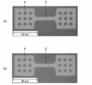
- (A) is the optical micrograph which showed the surface of the thin film pattern before transcription
- (b) is the optical micrograph which showed the surface of the thin film pattern after transcription
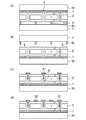
- FIGS. 4A to 4E are process diagrams showing a method of manufacturing a thin film transistor using the thin film transfer technique according to the present invention.
- FIGS. 4A to 4D are process diagrams showing a method of manufacturing a thin film transistor using the thin film transfer technique according to the present invention.
- (A) is the top view which showed the shape of the patterned single crystal silicon film
- (b) is the top view which showed the shape of the single crystal silicon film
- (A)-(d) is process drawing which showed the other manufacturing method of the thin-film transistor in this invention.
- FIG. 6 is a graph showing I DS -V GS characteristics of a thin film transistor (insulating film is only a thermal oxide film) formed by being transferred to a flexible substrate.
- (A), (b) is the SEM photograph which showed the state of the channel area
- (A), (b) is the optical microscope photograph which showed the state of the silicon film after transferring the silicon film of a hollow structure to a glass substrate. It is the graph which showed the displacement of the silicon film with respect to the film thickness of a thermal oxide film. It is a top view of the single crystal silicon film pattern formed in the matrix form.
- FIGS. 4A to 4E are process diagrams showing a method for manufacturing an amorphous silicon thin film transistor.
- FIGS. 4A to 4D are process diagrams showing a method for manufacturing an amorphous silicon thin film transistor.
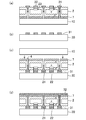
- (A)-(d) is process drawing which showed the manufacturing method of the solar cell using the transfer technique of the thin film in this invention.
- (A)-(e) is process drawing which showed the manufacturing method of the solar cell using the transfer technique of the thin film in this invention.
- (A)-(e) is process drawing which showed the other manufacturing method of the solar cell using the transfer technique of the thin film in this invention.
- (A)-(d) is process drawing which showed the other manufacturing method of the solar cell using the transfer technique of the thin film in this invention.
- (A)-(d) is process drawing which showed the other manufacturing method of the solar cell using the transfer technique of the thin film in this invention.
- the inventors of the present application have disclosed a technique for transferring an amorphous silicon film formed on a transfer source quartz substrate to a transfer destination substrate (glass substrate or flexible substrate) simultaneously with crystallization, as disclosed in Japanese Patent Application No. 2011-176335. It is disclosed in the document.
- this transfer technology an opening is formed in an amorphous silicon film, and the quartz substrate is etched through the opening to form a hollow structure of the amorphous silicon film supported by the quartz pillar.
- laser irradiation is performed from the quartz substrate side to melt and recrystallize the amorphous silicon film. Since the crystallized silicon film has strong chemical bonds with the transfer destination substrate, the crystallized silicon film is transferred to the transfer destination substrate.
- the inventors of the present application pay attention to a single crystal silicon film formed on an SOI (Silicon on Insulator) substrate, and a technique for transferring the single crystal silicon film to a substrate such as a quartz substrate, a glass substrate, or a flexible substrate.
- SOI Silicon on Insulator
- the present invention has been studied and conceived.
- (First embodiment) 1 and 2 are process diagrams showing a thin film forming method according to the first embodiment of the present invention.
- a first substrate 1 having a thin film 2 formed on a surface with a sacrificial layer 3 interposed therebetween is prepared.
- a substrate for example, an SOI substrate can be used.
- the first substrate 1 is a single crystal silicon substrate
- the thin film 2 is a single crystal silicon film
- the sacrificial layer 3 is a silicon oxide film.
- a plurality of openings 4 are formed in the thin film 2.
- the opening 4 can be formed by etching using, for example, a photolithography process.
- the sacrificial layer 3 is etched through the opening 4 to form a hollow portion 5 between the first substrate 1 and the thin film 2.
- the sacrificial layer 3 is a silicon oxide film, it can be etched using hydrofluoric acid. Etching is preferably performed using an etching solution having a high etching selectivity between the thin film 2 and the first substrate 1.
- a liquid (not shown) is interposed between the thin film 2 and the second substrate 10, and the second substrate 10 is adhered to the thin film 2.
- the liquid is filled between the thin film 2 and the second substrate 10, and the opening 4 and the hollow portion 5 are also filled with the liquid.
- the second substrate 10 for example, a quartz substrate, a glass substrate, a flexible substrate, or the like can be used.
- water, ethanol, acetone, etc. can be used for a liquid, for example.
- a liquid having a large surface tension (such as water) is preferable.
- the first substrate 1 and / or the second substrate 10 is heated.
- the heating is performed at a temperature below the boiling point of the liquid, and can be performed using, for example, a halogen lamp or a hot plate.
- the heating step is intended to dry the liquid interposed between the thin film 2 and the second substrate 10 and the liquid filling the opening 4 and the hollow portion 5, and is not necessarily the first. It is not necessary to directly heat both the substrate 1 and the second substrate 10. For example, a method of heating one substrate and indirectly heating the other substrate may be used.
- the liquid interposed between the thin film 2 and the second substrate is dried, so that the thin film 2 is separated from the first substrate 1. Accordingly, when the second substrate 10 is pulled up, the thin film 2 is transferred to the second substrate 10. At this time, the thin film 2 is transferred to the second substrate 10 with the pattern in which the opening 4 is formed. Further, the pillar 3 a made of a part of the sacrificial layer 3 remains on the first substrate 1.
- the thin film 2 formed on the first substrate 1 is transferred to the second substrate 10 as it is. Therefore, if the thin film 2 is a single crystal film, the single crystal film is transferred to the second substrate 10 as it is.
- a single crystal semiconductor thin film can be formed on a substrate such as a quartz substrate, a glass substrate, or a flexible substrate.
- FIG. 3A is a plan view of the thin film 2 in which a plurality of openings 4 are formed. As shown in FIG. 3A, the plurality of openings 4 are formed in an array. Then, an etching solution for etching the sacrificial layer 3 is supplied through the opening 4 so that the sacrificial layer 3 is isotropically etched. When the etching for the thickness of the sacrificial layer 3 proceeds, the etching further proceeds along the direction parallel to the film of the sacrificial layer 3. A dotted line in FIG. 3A indicates the boundary of the sacrificial layer 3 when etching proceeds in a direction parallel to the film of the sacrificial layer 3 with the opening 4 as the center.
- FIG. 3 (b) and 3 (c) are cross-sectional views showing this state
- FIG. 3 (b) is a cross-sectional view taken along line IIIb-IIIb in FIG. 3 (a)
- FIG. FIG. 3 (a) is a cross-sectional view taken along IIIc-IIIc.
- a hollow portion 5 is formed between the first substrate 1 and the thin film 2 at a position along IIIb-IIIb. As shown, the hollow portion 5 is not yet formed at the location along IIIc-IIIc.
- the sacrificial layer 3 between the first substrate 1 and the thin film 2 is all etched at a location along IIIb-IIIb so that only the hollow portion 5 is formed.
- a column 3a made of a part of the sacrificial layer 3 remains at a position along IIIc-IIIc.
- the thin film 2 has a hollow structure supported by the pillars 3a arranged in an array.
- the etching of the sacrificial layer 3 is controlled by time management or the like so that the size of the pillar 3a becomes a transferable size described later. Since the pillar 3a is formed by etching in a direction parallel to the film of the sacrificial layer 3, the pillar 3a having a predetermined size can be formed with good control.
- FIG. 5A shows a state in which the liquid 20b is interposed between the thin film 2 and the second substrate 10 so that the second substrate 10 is in close contact with the thin film 2 as shown in FIG. 1D. It is sectional drawing which showed. At this time, the opening 4 and the hollow portion 5 are also filled with the liquid 20a.
- FIG. 5A for convenience of explanation, the opening 4 shown in FIG. 4B and the column 3a shown in FIG. 4C are shown in the same cross section.
- the liquid 20b interposed between the thin film 2 and the second substrate 10 is drawn with an exaggerated thickness.
- FIG. 6A is an enlarged cross-sectional view of a region indicated by a circle A in FIG.
- the liquid 20b interposed between the thin film 2 and the second substrate 10 forms a capillary bridge, and a capillary adhesive force (meniscus force) is acting on the thin film 2 supported by the column 3a.
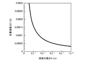
- the magnitude of the capillary adhesive forces, the liquid 20b height (height of the bridge) H depends on the contact area between the thin film 2 and the liquid 20b, and degree of contact theta E.
- Figure 7 is a liquid and water, the membrane 2 and the contact area (one area supporting at pillar 3a) of 9 .mu.m ⁇ 9 .mu.m with the liquid 20b, when formed into a 30 ° contact angle theta E, the height of the liquid 20b
- the magnitude of the capillary adhesion was determined as follows ("Physics of surface tension", Pierre-Gilles de Gennes, Francoise Brochard-Wyart, David Quere), Takeshi Okumura (translation): (See 2nd edition (2008) p.6-9).
- the adhesion force of the substrate that is, the capillary adhesion force F is an attractive force and is expressed by the following equation.
- the capillary adhesive force F depends on the contact area between the thin film 2 and the liquid 20b, and the bonding force between the first substrate 1 and the pillar 3a depends on the contact area between the first substrate 1 and the pillar 3a.
- the pillars 3 a are formed in an array at the same interval as the opening 4.
- the thin film 2 surrounded by the four openings 4 in the 2 ⁇ 2 array is supported by the single pillar 3a at the center. Therefore, the area of the thin film 2 supported by one column 3a, that is, the contact area between the thin film 2 and the liquid 20b can be adjusted by changing the interval between the openings 4.
- the contact area between the first substrate 1 and the pillar 3a can be adjusted by changing the cross-sectional area (size) of the pillar 3a.
- the cross-sectional area of the pillar 3 a can be changed by adjusting the etching amount of the sacrificial layer 3 in the step of forming the hollow portion 5.
- the capillary adhesive force F by the liquid interposed between the thin film 2 and the second substrate 10 is when the contact angle ⁇ E of the liquid in contact with the thin film 2 is less than 90 °, as shown in FIG. Act on. Therefore, it is more preferable that the second substrate 10 is hydrophilic to the liquid. Therefore, when the second substrate 10 is made of a material that is not hydrophilic with respect to the liquid, it is preferable to perform a surface treatment that makes the surface of the second substrate 10 hydrophilic.
- the surface treatment for imparting hydrophilicity can be performed, for example, by forming a polar thin film on the surface of the second substrate 10.
- substrate 10 is a flexible substrate, it can carry out by apply
- the transfer of the thin film 2 to the second substrate 10 is performed by using the capillary adhesive force of the liquid 20b interposed between the thin film 2 and the second substrate 10, but actually In the surface of the thin film 2 and the surface of the second substrate, the liquid 20b interposed between the thin film 2 and the second substrate 10 varies depending on the location. Therefore, the capillary adhesive force also varies depending on the location. Therefore, if the liquid 20b is dried all over the substrate all at once, the transfer proceeds from various directions, and the thin film 2 transferred to the second substrate 10 may be wrinkled.
- FIG. 8 is a process diagram showing a method of heating a substrate that has improved this problem.
- FIG. 8A shows the same state as FIG. 5A.
- the column 3a is not shown for convenience of explanation.
- the first substrate 1 and the second substrate 10 are heated so that the liquid evaporates in a certain direction from the end portions of the substrates 1 and 10, first, the first substrate 1.
- the gap between the thin film 2 and the second substrate 10 passes through the opening 4 from the side close to the end (left side in the figure).
- the liquid 20b intervening in the vapor passes through the hollow portion 5 and evaporates to the outside.
- the liquid 20b interposed between the thin film 2 near the ends of the substrates 1 and 10 and the second substrate 10 evaporates, so that the thin film 2 in that portion is separated from the pillar 3a (not shown), Transferred to the second substrate 10.
- the transfer timing can be controlled by heating the first substrate 1 and the second substrate 10 so that the liquid evaporates from the end portions of the substrates 1 and 10 along a certain direction. .
- the thin film 2 can be transferred to the second substrate 10 without wrinkles.
- the transfer technique in the present invention utilizes the difference between the capillary adhesive force acting on the thin film 2 by the liquid 20b existing between the thin film 2 and the second substrate 10 and the bonding force between the thin film 2 and the column 3a.
- the thin film 2 is transferred to the second substrate 10. Therefore, in order to reliably transfer the thin film 2 to the second substrate 10, the amount of liquid supplied between the thin film 2 and the second substrate, the heating temperature for evaporating the liquid, and the hollow
- the size of the pillar 3a that supports the structural thin film 2 is an important parameter.
- FIGS. 9 to 11 are graphs showing the results of measuring the transfer rate with respect to these parameters.
- an SOI substrate in which a single crystal silicon thin film (thickness: 180 nm) is formed on a silicon substrate via a silicon oxide film (thickness: 500 nm) is used as the first substrate 1.
- a PET (polyethylene terephthalate) substrate was used as the second substrate 10.
- the thin film (single crystal silicon film) 2 has openings 4 having a size of 2 ⁇ m ⁇ 2 ⁇ m formed in an array shape with a pitch of 11 ⁇ m, and pillars 3 a that support the hollow single crystal silicon film are 1 ⁇ m ⁇ 1 ⁇ m. It was made the size.
- the hollow structure was formed in a region of 6 mm ⁇ 6 mm in the first substrate 1. Moreover, water was used as the liquid. Further, the transfer rate was calculated from (transferred Si film area) / (Si film area before transfer) ⁇ 100 (%).
- FIG. 9 is a graph showing the result of measuring the transfer rate of the thin film 2 with respect to the amount of liquid (water) supplied between the thin film 2 and the second substrate 10.
- the liquid (water) is supplied by dropping 2 ⁇ l to 8 ⁇ l of water with a pipette into the center of the area (6 mm ⁇ 6 mm) where the hollow structure is formed, and then bringing it into close contact with the transfer destination substrate. It was.
- a transfer rate of 100% can be realized without depending on the amount of liquid to be supplied.
- the transfer rate decreased to 80% when the amount of liquid was 2 ⁇ l because the supply of liquid was insufficient and a region where no liquid was present was formed between the thin film 2 and the second substrate depending on the location. it is conceivable that.
- the transfer rate was 0%. This is because no liquid is present between the thin film 2 and the second substrate 10, so that the capillary adhesive force that separates from the column 3 a does not act on the thin film 2 at all.
- FIG. 10 is a graph showing the result of measuring the transfer rate of the thin film 2 with respect to the heating temperature for evaporating the liquid (water) interposed between the thin film 2 and the second substrate.
- the heating temperature is 30 ° C. or higher, a transfer rate of 100% can be realized. This means that the transfer rate does not depend on the drying speed, but is limited by the capillary adhesive force acting on the thin film 2. Note that heating at a temperature equal to or higher than the boiling point of the liquid (100 ° C. or higher in the case of water) is not preferable because the quasi-static capillary adhesive force does not act on the thin film 2 and uniform transfer cannot be performed.
- FIG. 11 is a graph showing the result of measuring the transfer rate of the thin film 2 with respect to the size of the pillar 3a supporting the thin film 2 having a hollow structure.
- the transfer rate of the thin film 2 is 100%.
- the transfer rate decreased as the size of the pillar 3a increased. This is because the capillary adhesion force acting on the thin film 2 by the liquid 20b interposed between the thin film 2 and the second substrate 10 is larger than the bonding force between the thin film 2 and the column 3a. This suggests that the thin film 2 is transferred to the second substrate 10.
- the graphs shown in FIGS. 9 to 11 give guidelines on how to set important parameters that contribute to the transfer in order to transfer the thin film 2 to the second substrate 10 with certainty. It is. Therefore, the numerical values shown in the graph vary depending on the shape of the hollow structure, the materials of the substrates 1, 10 and the thin film 2, the sacrificial layer 3, the liquid to be supplied, and the like, and do not make an absolute meaning.
- FIG. 12 (a) is an optical micrograph showing the surface of the thin film 2 before transfer
- FIG. 12 (b) is an SEM (scanning electron microscope) photo showing the surface of the thin film 2 after transfer.
- an SOI substrate was used as the transfer source substrate, and the openings 4 were formed in a staggered pattern.
- a glass substrate was used as the transfer destination substrate.
- FIG. 12B the thin film 2 is transferred to the transfer destination substrate while the opening 4 is formed.
- FIG. 12C shows an EBSD (electron beam backscatter diffraction) image of the thin film (single crystal silicon film) after transfer, and the single crystal silicon film having a uniform crystal orientation of (100) is transferred. It could be confirmed.
- EBSD electron beam backscatter diffraction
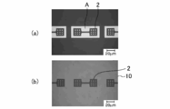
- FIG. 13A is an optical micrograph showing a thin film pattern before transfer when the thin film 2 is formed into a thin film transistor pattern to be described later, and FIG. 13B shows the thin film pattern after transfer. It is the optical microscope photograph.
- an SOI substrate was used as the transfer source substrate, and the opening 4 was formed in the source / drain region of the thin film transistor.
- a flexible substrate was used as the transfer destination substrate. As shown in FIG. 13B, the thin film 2 is transferred to the transfer destination substrate in the pattern in which the opening 4 is formed.
- FIG. 14 is a cross-sectional SEM photograph showing the state of the thin film 2 having a hollow structure. As shown in FIG. 14, it can be seen that the thin film 2 in which the hollow portion 5 is formed is supported by the pillar 3a while maintaining the film shape.
- the hollow portion 5 is formed by etching the sacrificial layer 3 through the opening 4 formed in the thin film 2. Therefore, the arrangement of the pillars 3 a remaining after the etching of the sacrificial layer 3 also changes depending on the arrangement of the openings 4.
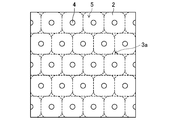
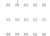
- FIG. 15 is a plan view showing an example in which the openings 4 are arranged in a staggered manner.
- the pillars 3 a are formed at six places surrounding the opening 4.
- the pillars 3 a are formed at four places surrounding the openings 4. Therefore, the number of columns 3a supporting the thin film 2 in the hollow state can be formed more by arranging the openings 4 in a zigzag pattern than arranging the openings 4 in an array pattern.
- the SOI substrate is described as an example of the transfer source substrate, but the present invention is not limited to this, and substrates of various materials can be used.
- the first substrate may be a quartz substrate or a glass substrate.
- the transferred thin film 2 may be a polycrystalline silicon film or an amorphous silicon film.
- Other semiconductor thin films for example, germanium film, silicon carbide (SiC) film, hydrogenated amorphous silicon (a-Si: H) a film or the like.
- the thin film 2 to be transferred may be an insulating film such as an oxide film or other films.
- the liquid interposed between the thin film and the second substrate is not particularly limited, and for example, perhydropolysilazane may be used in addition to water, ethanol, and acetone.
- perhydropolysilazane when perhydropolysilazane is used, when the polysilazane evaporates, capillary adhesion acts on the thin film, and in addition to the change in the molecular structure (silica conversion) of the perhydropolysilazane, Since the polysilazane is chemically bonded, the chemical bonding force further acts on the thin film, so that it can be transferred to the second substrate.
- the shape of the opening 4 formed in the thin film 2 is not particularly limited, and may be, for example, a rectangle or a circle. Further, the arrangement of the openings 4 is not limited to an array (including a matrix), and may include, for example, an irregular arrangement.
- the thin film 2 is transferred to the second substrate 10 as it is, but the thin film 2 is transferred to further improve the adhesion between the thin film 2 and the second substrate 10.
- a step of heat treating the second substrate 10 may be further added.
- the second substrate 10 as a transfer destination is a flexible substrate made of PET (polyethylene terephthalate) resin
- PET polyethylene terephthalate
- the heat treatment temperature is 150 ° C. or higher
- the PET substrate is altered, and therefore, the heat treatment temperature is preferably less than 150 ° C.
- heat treatment can be performed by performing laser irradiation.
- a thermal plasma jet, a flash lamp, an electric furnace or the like may be used.
- the transfer source substrate described in the first embodiment a substrate in which the thin film 2 is formed on the first substrate 1 with the sacrificial layer 3 interposed therebetween is used.
- the hollow portion 5 is formed by etching the sacrificial layer 3 through the opening 4 formed in the thin film 2. That is, the height of the hollow portion 5 is regulated by the thickness of the sacrificial layer 3.
- the hollow portion 5 can be formed without using the sacrificial layer 3.
- a method of transferring a thin film 2 to a second substrate using a transfer substrate having a thin film 2 formed on a first substrate will be described.
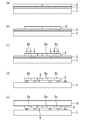
- 16 and 17 are process diagrams showing a thin film forming method according to the second embodiment of the present invention.
- a first substrate 1 having a thin film 2 formed on the surface is prepared.
- a substrate for example, a substrate in which an amorphous silicon film is formed on a quartz substrate can be used.
- a plurality of openings 4 are formed in the thin film 2.
- the opening 4 can be formed by etching using, for example, a photolithography process.
- the first substrate 1 is etched through the opening 4 to form a hollow portion 5 between the first substrate 1 and the thin film 2.
- etching can be performed using hydrofluoric acid.
- the height of the hollow portion 5 is substantially the same as the lateral etching length of the first substrate 1.
- a liquid (not shown) is interposed between the thin film 2 and the second substrate 10, and the thin film 2 is brought into close contact with the second substrate 10.
- the second substrate 10 for example, a quartz substrate, a glass substrate, a flexible substrate, or the like can be used.
- water, ethanol, acetone, etc. can be used for a liquid, for example.
- the first substrate 1 and / or the second substrate 10 is heated.
- the heating is performed at a temperature below the boiling point of the liquid, and can be performed using, for example, a halogen lamp or a hot plate.
- This heating step is intended to dry the liquid interposed between the thin film 2 and the second substrate 10, and both the first substrate 1 and the second substrate 10 are not necessarily heated directly.
- a method of heating one substrate and indirectly heating the other substrate may be used.
- the liquid interposed between the thin film 2 and the second substrate 10 is dried, so that the thin film 2 is separated from the first substrate 1. Accordingly, when the second substrate 10 is pulled up, the thin film 2 is transferred to the second substrate 10. At this time, the thin film 2 is transferred to the second substrate 10 with the pattern in which the opening 4 is formed. Further, the pillar 1 a that is a part of the first substrate 1 remains on the surface of the first substrate 1.
- the transfer mechanism in the present embodiment is basically the same as the transfer mechanism in the first embodiment. That is, using the difference between the capillary adhesive force acting on the thin film 2 by the liquid interposed between the thin film 2 and the second substrate 10 and the bonding force between the thin film 2 and the pillar 1a, the thin film 2 is Can be transferred to the substrate 10.
- the quartz substrate having the thin film 2 formed on the surface is described as an example of the transfer source substrate.
- the present invention is not limited to this, and substrates of various materials can be used.
- the first substrate may be a silicon substrate or a glass substrate.
- the transferred thin film 2 may be a polysilicon film, and may be another semiconductor thin film (for example, a germanium film, a silicon carbide (SiC) film, a hydrogenated amorphous silicon (a-Si: H) film, etc.). There may be.
- the thin film 2 to be transferred may be an insulating film such as an oxide film or other films.
- the liquid interposed between the thin film and the second substrate is not particularly limited, and for example, perhydropolysilazane may be used in addition to water, ethanol, and acetone.
- perhydropolysilazane when perhydropolysilazane is used, when the polysilazane evaporates, capillary adhesion acts on the thin film, and in addition to the change in the molecular structure (silica conversion) of the perhydropolysilazane, Since the polysilazane is chemically bonded, the chemical bonding force further acts on the thin film, so that it can be transferred to the second substrate.
- the shape of the opening 4 formed in the thin film 2 is not particularly limited, and may be, for example, a rectangle or a circle. Further, the arrangement of the openings 4 is not limited to an array (including a matrix), and may include an irregular arrangement, for example.
- the thin film 2 is transferred to the second substrate 10 as it is, but the thin film 2 is transferred to further improve the adhesion between the thin film 2 and the second substrate 10.
- a step of heat treating the second substrate 10 may be further added.
- the thin film formed on the transfer source substrate can be transferred to the transfer destination substrate (second substrate) maintaining the film quality, and the transfer source substrate and the transfer destination substrate can be transferred.
- a substrate can be arbitrarily selected. Therefore, for example, by transferring a single crystal silicon film formed on an SOI substrate to a glass substrate or a flexible substrate, the plane orientation is completely controlled on the glass substrate or the flexible substrate, which has conventionally been difficult.
- a single crystal silicon film can be formed.
- FIGS. 18 and 19 are process diagrams showing a method of manufacturing a thin film transistor (field effect transistor) using the thin film transfer technique of the present invention.
- silicon film 2 a p-type single crystal silicon film (hereinafter simply referred to as “silicon film”) 2 is formed on a silicon substrate 1 with a silicon oxide film 3 interposed therebetween.
- the p-type silicon film 2 is patterned into regions that will be the source / drain and channel of the transistor.
- the source / drain regions 2b and 2c are doped with n-type impurities (for example, phosphorus) by ion implantation, and then heat treatment (for example, about 600 to 1000 ° C.) is performed. Then, the impurities are activated.
- n-type impurities for example, phosphorus
- the silicon oxide film 3 is isotropically etched with hydrofluoric acid through the opening to obtain the silicon substrate 1.
- a hollow portion 5 is formed between the silicon film 2 and the silicon film 2.
- the silicon film 2 has a hollow structure supported by the pillars 3 a left by the etching of the silicon oxide film 3.
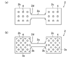
- FIG. 20 (a) is a plan view showing the shape of the patterned silicon film 2
- FIG. 20 (b) is a plan view showing the shape of the silicon film 2 having a hollow structure.
- the opening 4 is formed only in the region to be the source / drain regions 2b and 2c, and is not formed in the region to be the channel region 2a.
- the openings 4 are formed in a matrix (3 ⁇ 3), and a connecting portion 2d is formed at the boundary between the channel region 2a and the source / drain regions 2b and 2c.
- a hollow silicon film 2 supported by a plurality of pillars 3a is formed as shown in FIG.
- the pillar 3a is formed only in the source / drain regions 2b and 2c, and the channel region 2a is in a completely floating hollow state.
- the plurality of pillars 3a are formed over the entire source / drain regions 2b and 2c, and the pillar 3b is also formed in the connecting portion 2d, the hollow channel region 2a is stably supported. be able to.
- FIG. 21 is a SEM photograph of the hollow structure silicon film 2 prepared by the above method. As shown in FIG. 21, it can be seen that the film shape is maintained even when the silicon film is hollow.
- water (not shown) is interposed between the silicon film 2 and the flexible substrate 10 to bring the silicon film 2 into close contact with the flexible substrate 10.
- the silicon substrate 1 and / or the flexible substrate 10 is heated. Thereby, the water interposed between the silicon film 2 and the flexible substrate 10 is dried, so that the silicon film 2 is separated from the silicon substrate 1 and transferred to the flexible substrate 10. Thereafter, the flexible substrate 10 to which the silicon film 2 is transferred is heat-treated.
- the flexible substrate 10 is a PET substrate
- heat treatment is preferably performed at a temperature of about 120 ° C. Thereby, the bonding force between the silicon film 2 and the flexible substrate 19 can be further increased.
- a gate insulating film 11 is formed on the transferred silicon film 2.
- the gate insulating film 11 can be formed, for example, by coating using a polysilazane solution.
- a gate electrode 12 is formed on the gate insulating film 11.
- the gate electrode can be formed by, for example, aluminum vapor deposition, sputtering, or an ink jet method using metal nanoparticles.
- an interlayer insulating film 13 is formed on the gate electrode 12
- openings are formed in the interlayer insulating film 13 and the gate insulating film 11, and source / Drain electrodes 14 and 15 are formed.
- the interlayer insulating film 13 can be formed by, for example, coating
- the source / drain electrodes can be formed by, for example, sputtering of aluminum, vapor deposition, or an ink jet method using metal nanoparticles.
- a thin film transistor made of a single crystal silicon film can be manufactured on the flexible substrate 10 by using the thin film transfer technique of the present invention. Also, if this transfer technology is used, activation of the source / drain which requires a high-temperature process is performed on the SOI substrate as the transfer source, and the flexible substrate 10 with low heat resistance at the transfer destination is gated by the low-temperature process. An insulating film, an electrode, or the like can be formed. Thereby, a high-performance thin film transistor can be realized with little variation.
- the interface state between the silicon film 2 and the gate insulating film 11 in the channel region 2a affects the characteristics of the thin film transistor.
- a method for improving the interface state it is effective to improve the film quality of the gate insulating film 11.
- a method for improving the film quality of the gate insulating film 11 by heat-treating the gate insulating film 11 formed on the flexible substrate 10 having low heat resistance at a high temperature cannot be employed.
- the surface of the silicon film 2 is thermally oxidized before the silicon film 2 is transferred to the flexible substrate 10. It is conceivable to form a thermal oxide film on the surface of the silicon film 2. In this case, since a thermal oxide film having a good film quality is interposed between the silicon film 2 in the channel region 2a and the gate insulating film 11, the silicon film 2 in the channel region 2a and the gate insulating film 11 The interface state can be made favorable.
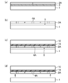
- FIGS. 22A to 22D show a method for improving the interface state between the silicon film 2 and the gate insulating film 11 in the channel region 2a in the method for manufacturing the thin film transistor shown in FIGS. It is process drawing.
- the steps shown in FIGS. 22B to 22D are the same as the steps shown in FIGS. 18E and 19A to 19B.
- FIG. 22A the silicon oxide film 3 is isotropically etched through the opening 4 formed in the silicon film 2 as shown in FIG.
- FIG. 2 is a diagram in which after the hollow portion 5 is formed, the surface of the silicon film 2 supported by the pillar 3 a made of the silicon oxide film 3 is thermally oxidized to form a thermal oxide film 16 on the surface of the silicon film 2.
- Thermal oxidation may be performed, for example, in an oxygen atmosphere at a temperature of 800 to 1100 ° C., and a thermal oxide film 16 of about 2 to 15 nm may be formed on the surface of the silicon film 2.
- the thermal oxide film 16 having the same film thickness as the surface of the silicon film 2 opened outward (upper surface in the drawing) is formed.
- the substantially uniform thermal oxide film 16 is formed over the entire surface of the silicon film 2. It is formed. In this thermal oxidation step, activation of the impurities ion-implanted into the source / drain regions 2b and 2c can be performed simultaneously.
- water (not shown) is interposed between the silicon film 2 and the flexible substrate 10 to bring the silicon film 2 into close contact with the flexible substrate 10.
- the silicon substrate 1 and / or the flexible substrate 10 is heated. Thereby, the water interposed between the silicon film 2 and the flexible substrate 10 is dried, so that the silicon film 2 is separated from the silicon substrate 1 and transferred to the flexible substrate 10.
- a gate insulating film 11 is formed on the transferred silicon film 2.
- the thermal oxide film 16 is interposed between the silicon film 2 in the channel region 2a and the gate insulating film 11, the interface state between the silicon film 2 and the gate insulating film 11 in the channel region 2a. Can be improved.
- the gate electrode 12 and the source / drain electrodes 14 and 15 are formed to complete the thin film transistor.
- the gate insulating film 11 is further formed on the thermal oxide film 16, but when the thermal oxide film 16 has a film thickness sufficient to obtain predetermined characteristics of the thin film transistor.
- the thermal oxide film 16 may be used as it is as the gate insulating film.
- the thermal oxidation condition takes into account the impurity concentration (particularly, the impurity concentration in the source / drain regions 2 b and 2 c). You only have to set it. Alternatively, the impurity concentration may be adjusted as appropriate in order to obtain the thermal oxide film 16 having a predetermined thickness.
- FIG. 23A and 23B are graphs showing the results of evaluating the characteristics of the thin film transistor manufactured by such a method.
- FIG. 23A is a graph showing a change in drain current (I DS ) with respect to a gate-source voltage (V GS ) (I DS -V GS characteristic) and a change in field effect mobility.
- FIG. 23B is a graph showing a change (I DS -V DS characteristic) of the drain current (I DS ) with respect to the drain-source voltage (V DS ).
- the manufactured thin film transistor was an n-channel field effect transistor having a channel length of 4 ⁇ m (an effective channel length of 3.7 ⁇ m) and a channel width of 3 ⁇ m.
- the film thickness of the thermal oxide film 16 was 10 nm, and the film thickness of the gate insulating film 11 was 206 nm.
- the transfer destination substrate 10 was a glass substrate.
- the maximum value of the field effect mobility was 742 cm 2 V ⁇ 1 s ⁇ 1 and the threshold value was 1.5V.
- the subthreshold leakage current was about 1 ⁇ 10 ⁇ 13 A, and the on / off ratio of the drain current (I DS ) was about 8 digits.
- Such high performance as a thin film transistor indicates that the silicon film 2 transferred to the glass substrate 10 is a single crystal, and the interface state between the silicon film 2 and the gate insulating film 11 in the channel region 2a is It shows that it is favorable.
- the surface of the silicon film 2 is thermally oxidized, and the thermal oxide film 16 is formed on the surface of the silicon film 2.
- a high performance thin film transistor can be obtained.
- the glass substrate to which the silicon film 2 is transferred in order to improve the adhesion between the silicon film 2 and the glass substrate 10. 10 may be heat-treated.
- impurities contained in the glass substrate 10 for example, alkali metal or the like present on the substrate surface or inside the substrate
- the impurity forms a mobile ion or a trap level, which may cause a decrease in leakage current, mobility, or reliability.
- the thermal oxide film 16 is interposed between the glass substrate 10 and the silicon film 2, the thermal oxide film 16 is doped with impurities from the glass substrate 10 into the silicon film. 2 is a barrier to prevent diffusion into Therefore, even if impurities serving as a contamination source are present in the glass substrate 10 as a transfer destination, it is possible to prevent deterioration of the characteristics of the thin film transistor due to diffusion of the impurities.
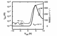
- FIG. 24 shows the result of evaluation of I DS -V GS characteristics by manufacturing a thin film transistor under the same conditions as above using a PET substrate (flexible substrate) instead of a glass substrate as the transfer destination substrate 10. It is a graph.
- the maximum value of the field effect mobility was 343 cm 2 V ⁇ 1 s ⁇ 1 and the threshold value was 3.9 V.
- the subthreshold leakage current was about 6 ⁇ 10 ⁇ 10 A, and the on / off ratio of the drain current (I DS ) was about 4 digits.
- FIG. 25 is a graph showing a result of manufacturing a thin film transistor using a PET substrate (flexible substrate) instead of a glass substrate as the transfer destination substrate 10 and evaluating the I DS -V GS characteristics.
- the thermal oxide film 16 having a film thickness of 10 nm is used as it is as the gate insulating film without forming the gate insulating film 11 on the thermal oxide film 16.
- the thin film transistor was manufactured under the same conditions as those shown in FIG.
- the maximum value of the field effect mobility was 627 cm 2 V ⁇ 1 s ⁇ 1 and the threshold value was 0.07 V.
- the subthreshold leakage current was 1.3 ⁇ 10 ⁇ 12 A, and the on / off ratio of the drain current (I DS ) was about 7 digits.
- the gate insulating film 11 on the thermal oxide film 16 is formed by a low temperature process (for example, deposition using plasma CVD or coating using a polysilazane solution), so that the quality of the oxide film is higher than that of the thermal oxide film. Although it is inferior and the leak current becomes large, it is considered that when the gate insulating film is only the thermal oxide film 11, the leak current is suppressed.
- a low temperature process for example, deposition using plasma CVD or coating using a polysilazane solution
- the silicon film 2 before transfer has a hollow structure supported by a plurality of pillars 3a.
- the channel region 2a is in a completely floating hollow state.
- the thermal oxide film 16 is formed on the surface of the silicon film 2 having such a hollow structure, volume expansion occurs when the surface of the silicon film 2 is changed to the thermal oxide film 16 by thermal oxidation. Therefore, the formed thermal oxide film 16 may be warped in the hollow silicon film 2 when stress is applied to the silicon film 2.
- FIGS. 26A and 26B are SEM photographs showing the state in the vicinity of the channel region 2a when a 10 nm thick thermal oxide film 16 is formed on the surface of the silicon film 2 having a hollow structure.
- FIG. 26A is an SEM photograph when the channel length (L) is 5 ⁇ m
- FIG. 26B is an SEM photograph when the channel length (L) is 15 ⁇ m.
- FIGS. 27A and 27B are optical micrographs showing the state of the silicon film 2 after the silicon film 2 having the hollow structure shown in FIGS. 26A and 26B is transferred to the glass substrate 10. It is. As shown in FIG. 27A, when the channel length (L) is as short as 5 ⁇ m, the channel region 2a is completely transferred in contact with the glass substrate 10, but FIG. As shown, when the channel length (L) is as long as 15 ⁇ m, an interference color is observed in the channel region 2a, and a part of the channel region 2a is transferred to the glass substrate 10 while being floated from the glass substrate 10. Yes.
- thermal oxide films 16 having different thicknesses were formed on the silicon film 2 and the warpage of the silicon film 2 in the channel region 2a was measured.
- the warpage of the silicon film 2 was calculated by calculating the amount of displacement from the original position of the central portion of the channel region 2a from the SEM photograph of the silicon film 2 taken from an angle of 70 °.
- the original position was based on the height (300 nm) of the hollow portion 5 between the silicon substrate 1 and the silicon film 2.
- FIG. 28 is a graph showing the results. As shown in FIG. 28, the displacement of the silicon film 2 increases as the thickness of the thermal oxide film 16 increases. Further, when the thermal oxide film 16 has the same thickness, the displacement of the silicon film 2 increases as the channel length increases.
- the thermal deformation of the silicon film generated when the thermal oxide film 16 is formed on the surface of the silicon film 2 is considered. It is preferable to set the thickness of the oxide film 16.
- the conditions for transferring the silicon film 2 in close contact with the glass substrate 10 as a transfer destination are factors other than the warp of the silicon film 2, for example, in the state shown in FIG. Since it varies depending on the degree of adhesion between the transfer film 10 and the transfer destination substrate 10, the type of liquid interposed between the silicon film 2 and the flexible substrate 10, the heating conditions for drying the liquid, etc., it is not uniquely determined. If the displacement of the silicon film 2 is set to 50 nm or less, when the channel length is 5 ⁇ m, the film thickness of the thermal oxide film 16 is 12 nm or less, and when the channel length is 10 ⁇ m, the film thickness of the thermal oxide film 16 is 8 nm. The following should be set.
- the example in which the process of forming the thermal oxide film 16 on the surface of the silicon film 2 having the hollow structure is applied to the manufacturing process of the thin film transistor (field effect transistor) is not limited to this.
- a step of forming the thermal oxide film 16 on the surface of the silicon film 2 having a hollow structure can be employed before the transfer.
- the SOI substrate is used as the transfer source substrate.
- the present invention is not limited to this.
- a silicon substrate or a quartz substrate on which a polysilicon film is formed via an insulating film is used.
- a flexible substrate is used as a transfer destination substrate, the substrate is not limited to this, and for example, a quartz substrate, a glass substrate, a metal wheel substrate, a wafer having an integrated circuit, or the like can be used.
- the pattern of the silicon film 2 shown in FIG. 20A in a matrix as shown in FIG. 29, the pattern was arranged in a matrix on a transferable flexible substrate or a glass substrate.
- a thin film transistor can be formed.
- the opening 4 formed in the source / drain region is omitted. Accordingly, a high-performance liquid crystal display device can be manufactured by forming a wiring for driving the thin film transistor, a liquid crystal cell, or the like in a region where the thin film transistor is not formed.
- FIG. 30A is an optical micrograph showing the pattern of the silicon film 2 transferred to the glass substrate 10. As shown in FIG. 30B, it can be seen that only the pattern of the silicon film 2 formed in the region A is transferred to the glass substrate 10.
- the reason why a part of the silicon film 2 formed on the SOI substrate can be partially transferred to the glass substrate 10 is as follows. That is, since the silicon film 2 other than the region A is in contact with the insulating layer 3 over a large area, the silicon film 2 other than the region A than the capillary adhesive force acting on the silicon film 2 other than the region A The bond strength with the insulating layer 3 is greater. Therefore, it is considered that only the silicon film 2 in the region A in which the capillary adhesive force larger than the bonding force between the silicon film 2 and the pillar 3 a acts is transferred to the glass substrate 10.
- FIG. 31A is an optical micrograph showing the pattern of the silicon film 2 formed in the region B with respect to the silicon film 2 remaining after the first transfer
- FIG. 2 is an optical micrograph showing the pattern of the silicon film 2 transferred to the film. In this way, the portion remaining in the first transfer can be used for transfer again, and the silicon film 2 formed on the SOI substrate can be used effectively.
- 32 and 33 are process diagrams showing a method of manufacturing an amorphous silicon thin film transistor using the quartz substrate 1 having the amorphous silicon film 2 formed on the surface.
- an amorphous silicon film 2 doped with n-type impurities is deposited on the surface of the quartz substrate 1.
- a quartz substrate 1 on which an amorphous silicon film 2 doped with n-type impurities is deposited may be separately prepared.
- the amorphous silicon film 2 is etched to form source / drain regions.
- a non-doped amorphous silicon film 6 is deposited on the quartz substrate 1 to pattern the channel region.
- openings are formed in the amorphous silicon films 2 and 6, and then the quartz substrate 1 is isotropically etched with hydrofluoric acid through the openings.
- a hollow portion 5 is formed between the substrate 1 and the amorphous silicon films 2 and 6.
- the amorphous silicon films 2 and 6 have a hollow structure supported by the pillars 1 a left by the etching of the quartz substrate 1.
- water (not shown) is interposed between the amorphous silicon film 6 and the flexible substrate 10 so that the amorphous silicon film 6 is brought into close contact with the flexible substrate 10.
- the quartz substrate 1 and / or the flexible substrate 10 is heated. Thereby, the water interposed between the amorphous silicon film 6 and the flexible substrate 10 is dried, whereby the amorphous silicon films 2 and 6 are separated from the quartz substrate 1 and transferred to the flexible substrate 10.
- a gate insulating film 11 is deposited on the transferred amorphous silicon films 2 and 6.
- the gate insulating film 11 can be deposited, for example, by application using a polysilazane solution or by depositing a nitride film.
- the gate electrode 12 is formed on the gate insulating film 11.
- the gate electrode can be formed by, for example, sputtering of aluminum, vapor deposition, or an ink jet method using metal nanoparticles.
- FIGS. 34 and 35 are process diagrams showing a method of manufacturing a solar cell using the thin film transfer technique of the present invention.
- a single crystal silicon film (hereinafter simply referred to as “silicon film”) 2A doped with a p-type impurity is formed on a silicon substrate 1 via a silicon oxide film 3.
- a prepared SOI substrate is prepared.
- the silicon oxide film 3 is isotropically etched with hydrofluoric acid through the opening 4A to obtain the silicon substrate 1
- the p-type silicon film 2 are formed with a hollow portion 5.
- the p-type silicon film 2 has a hollow structure supported by columns (not shown) left by the etching of the silicon oxide film 3.
- a flexible substrate 10 having a transparent electrode 18 formed on the surface is prepared, and water (not shown) is interposed between the p-type silicon film 2 and the transparent electrode 18. Then, the silicon film 2 is brought into close contact with the flexible substrate 10.
- the silicon substrate 1 and / or the flexible substrate 10 is heated. Thereby, the water interposed between the p-type silicon film 2 and the transparent electrode 18 is dried, whereby the p-type silicon film 2 is separated from the silicon substrate 1 and transferred to the flexible substrate 10.
- an SOI substrate is prepared in which a silicon film 2B doped with an n-type impurity is formed on a silicon substrate 1 with a silicon oxide film 3 interposed therebetween.
- the silicon oxide film 3 is isotropically etched with hydrofluoric acid through the opening 4B to obtain the silicon substrate 1
- a hollow portion 5 is formed between the n-type silicon film 2B and the n-type silicon film 2B.
- the n-type silicon film 2B has a hollow structure supported by pillars (not shown) left by the etching of the silicon oxide film 3.
- water (not shown) is interposed between the n-type silicon film 2B and the p-type silicon film 2A transferred to the flexible substrate 10, so that the n-type silicon film 2B is adhered to the flexible substrate 10.
- the opening 4A formed in the p-type silicon film 2A and the opening 4B formed in the n-type silicon film 2B are brought into close contact with each other while being displaced from each other.
- the silicon substrate 1 and / or the flexible substrate 10 is heated. Thereby, the water interposed between the n-type silicon film 2B and the p-type silicon film 2A is dried, so that the n-type silicon film 2B is separated from the silicon substrate 1 and transferred to the flexible substrate 10.
- the electrode 17 is deposited on the transferred n-type silicon film 2B.
- the electrode 17 can be formed, for example, by vapor deposition of aluminum. Thereby, the solar cell which has the PN junction which consists of laminated
- the SOI substrate is used as the transfer source substrate.
- the present invention is not limited to this.
- a substrate in which a polysilicon film is formed on a silicon substrate or a quartz substrate via an insulating film is used. It may be used.
- the flexible substrate was used as a transfer destination substrate, it is not limited to this, and for example, a glass substrate or the like can be used.
- a step of heat treating the flexible substrate 10 may be further added to further improve the adhesion between the silicon films 2A and 2B and the flexible substrate 10. .
- 36 to 38 are process diagrams showing another method of manufacturing a solar cell using the thin film transfer technique according to the present invention.
- an SOI substrate is prepared in which a silicon film 2 doped with a p-type impurity is formed on a silicon substrate 1 via a silicon oxide film 3. Then, an opening 4 is formed in the silicon film 2.
- the silicon oxide film 3 is isotropically etched with hydrofluoric acid through the opening 4 to form a hollow portion 5 between the silicon substrate 1 and the silicon film 2. .
- the silicon film 2 has a hollow structure supported by the pillars 3 a left by the etching of the silicon oxide film 3.
- the surface of the p-type silicon film and the back surface facing the hollow portion 5 are textured.
- the texture processing can be performed, for example, by anisotropic etching with a TMAH (trimethylanilinium hydroxide) solution. If this method is used, the back surface facing the hollow portion 5 can be textured.
- TMAH trimethylanilinium hydroxide
- an n + layer is formed on the surface of the p-type silicon film 2.
- the n + layer can be formed, for example, by applying a phosphoric acid aqueous solution and then heating. If this method is used, the phosphoric acid aqueous solution is also introduced into the opening 4 and the hollow portion 5, so that the n + layer is also formed on the side surface of the opening 4 of the p-type silicon film 2 and the back surface facing the hollow portion 5. Can be formed.
- a silicon nitride film 7 is formed on the surface of the n + layer.
- the silicon nitride film 7 can be formed by using, for example, a plasma CVD method.
- water (not shown) is interposed between the silicon nitride film 7 and the glass substrate 10 so that the silicon nitride film 7 is adhered to the glass substrate 10.
- the silicon substrate 1 and / or the glass substrate 10 is heated. Thereby, the water interposed between the silicon nitride film 7 and the glass substrate 10 is dried, whereby the silicon film 2 and the silicon nitride film 7 are separated from the silicon substrate 1 and transferred to the glass substrate 10.
- the Ag electrode 21 is embedded in the opening 4.
- the embedding of the Ag electrode 21 can be performed by screen printing of Ag paste.
- an Al electrode 22 is formed on the surface of the n + layer.
- the Al electrode 22 can be formed by applying a paste material containing aluminum powder using screen printing or the like.
- the BSF (BackSurface Field) layer 23 is formed between the Al electrode 22 and the p-type silicon film 2 by baking the aluminum paste and diffusing aluminum into the n + layer. Form.
- a flexible substrate 30 having an electrode 31 formed on the surface is prepared, and formed on the glass substrate 10 using an adhesive as shown in FIG. 38C.
- the structured body including the PN junction is transferred to the flexible substrate 30.
- the Ag electrode 21 and the Al electrode 22 are joined to the electrode 31, respectively.
- an Ag electrode 32 is formed on the silicon nitride film 7 so as to fill the opening 4. Thereby, the solar cell formed in the flexible substrate 30 is manufactured.
- an electronic device is not limited to the thin-film transistor and solar cell which were demonstrated in the said application example, Various electronic containing a thin film as a component Applicable to devices.
Landscapes
- Chemical & Material Sciences (AREA)
- Crystallography & Structural Chemistry (AREA)
- Thin Film Transistor (AREA)
- Life Sciences & Earth Sciences (AREA)
- Sustainable Development (AREA)
- Engineering & Computer Science (AREA)
- Sustainable Energy (AREA)
- Photovoltaic Devices (AREA)
- Liquid Crystal (AREA)
Abstract
本発明の薄膜形成方法は、表面に薄膜2が形成された第1の基板1を用意する工程と、薄膜2に複数の開口部4を形成する工程と、開口部4を通じて第1の基板1をエッチングして、第1の基板1と薄膜2との間に中空部5を形成する工程と、薄膜2と第2の基板10との間に液体を介在させて、薄膜2第2の基板10に密着させる工程と、第1の基板1及び/又は第2の基板10を加熱する工程とを含み、加熱工程において、薄膜2と第2の基板10との間に介在する液体が乾燥することによって、薄膜2は、第1の基板1から引き離されて、第2の基板10に転写される。
Description
本発明は、薄膜形成方法、及びそれを用いて作製した半導体基板ならびに電子デバイスに関する。
薄膜トランジスタや太陽電池は、石英基板、ガラス基板、及びフレキシブル基板上に形成されたシリコン薄膜の結晶性によって、その性能が左右される。そのため、従来から、石英基板、ガラス基板、及びフレキシブル基板上に形成されたシリコン薄膜の結晶性を向上させる技術が盛んに研究されている。
石英基板、ガラス基板、及びフレキシブル基板上に多結晶シリコン膜を形成する代表的な方法として、レーザアニール法が知られている(特許文献1)。
石英基板、ガラス基板、及びフレキシブル基板上へのシリコン膜の形成技術の向上により、高結晶性のシリコン膜が実現されているが、石英基板、ガラス基板、及びフレキシブル基板上に単結晶シリコン膜を形成することは困難とされている。
本発明は、かかる課題に鑑みなされたもので、その主な目的は、石英基板、ガラス基板、フレキシブル基板等の基板上に、単結晶半導体膜等の薄膜を形成する薄膜形成方法、及びそれを用いて作製した半導体基板ならびに電子デバイスを提供することにある。
本発明の一実施形態における薄膜形成方法は、表面に薄膜が形成された第1の基板を用意する工程と、薄膜に複数の開口部を形成する工程と、開口部を通じて第1の基板をエッチングして、第1の基板と薄膜との間に中空部を形成する工程と、 薄膜と第2の基板との間に液体を介在させて、薄膜を第2の基板に密着させる工程と、第1の基板及び/又は前記第2の基板を加熱する工程とを含み、加熱工程において、薄膜と第2の基板との間に介在する液体が乾燥することによって、薄膜は、第1の基板から引き離されて、第2の基板に転写されることを特徴とする。
ある好適な実施形態において、上記薄膜は、犠牲層を挟んで第1の基板上に形成されており、上記中空部を形成する工程は、第1の基板の代わりに、犠牲層をエッチングすることにより行われ、上記加熱工程において、薄膜は、犠牲層から引き離されて、第2の基板に転写される。
本発明の一実施形態における半導体基板は、上記の薄膜形成方法により、表面に転写された半導体薄膜を備えた半導体基板を特徴とする。
本発明の一実施形態における電子デバイスは、上記の薄膜形成方法により、基板表面に転写された半導体薄膜を有する電子デバイスを特徴とする。
本発明の一実施形態における薄膜トランジスタの製造方法は、表面に絶縁層を挟んで半導体薄膜が形成された第1の基板を用意する工程と、半導体薄膜を、チャネル領域、及びソース・ドレイン領域となる領域にパターニングする工程と、ソース・ドレイン領域となる半導体薄膜に複数の開口部を形成する工程と、開口部を通じて絶縁層をエッチングして、絶縁層と半導体薄膜との間に中空部を形成する工程と、半導体薄膜と第2の基板との間に液体を介在させて、半導体薄膜を第2の基板に密着させる工程と、第1の基板及び/又は第2の基板を加熱する工程とを含み、加熱工程において、半導体薄膜と第2の基板との間に介在する液体が乾燥することによって、半導体薄膜のパターンが、第1の基板から引き離されて、第2の基板に転写されることを特徴とする。
ある好適な実施形態において、上記半導体薄膜のパターニング工程において、チャネル領域、及びソース・ドレイン領域となる領域が、マトリクス状にパターニングされる。
本発明の一実施形態における太陽電池の製造方法は、表面に透明電極が形成された第2の基板を用意する工程と、上記薄膜形成方法により、第1の基板から第2の基板に、第1導電型の半導体薄膜及び第2導電型の半導体薄膜を、順次転写する工程とを含み、転写工程において、透明電極上に、半導体薄膜からなるPN接合が形成させることを特徴とする。
本発明によれば、石英基板、ガラス基板、フレキシブル基板等の基板上に、単結晶半導体膜等の薄膜を形成する薄膜形成方法、及びそれを用いて作製した半導体基板ならびに電子デバイスを提供することができる。
本願発明者等は、転写元の石英基板上に形成されたアモルファスシリコン膜を、結晶化と同時に、転写先の基板(ガラス基板やフレキシブル基板)に転写する技術を、特願2011-176335の明細書に開示している。この転写技術は、アモルファスシリコン膜に開口部を形成し、この開口部を通じて、石英基板をエッチングすることにより、石英柱に支えられたアモルファスシリコン膜の中空構造を形成した後、転写先の基板をアモルファスシリコン膜に密着させた状態で、石英基板側からレーザ照射を行って、アモルファスシリコン膜を溶融、再結晶化させるというものである。そして、結晶化されたシリコン膜は、転写先の基板との化学結合が強いため、転写先の基板に転写される。
この転写技術によれば、ガラス基板やフレキシブル基板上に、大面積の結晶性の良いシリコン膜を形成することができるため、高性能の液晶パネル、太陽電池等の電子デバイスの実現が期待できる。
しかしながら、この転写技術は、アモルファスシリコン膜の溶融、再結晶化技術が必要となるため、転写先の基板に、大面積の単結晶シリコン膜を転写するには、まだ解決すべき課題を残す。
そこで、本願発明者等は、SOI(Silicon on Insulator)基板に形成された単結晶シリコン膜に注目し、この単結晶シリコン膜を、石英基板、ガラス基板、フレキシブル基板等の基板に転写する技術を検討し、本発明を想到するに至った。
以下、本発明の実施形態を図面に基づいて詳細に説明する。なお、本発明は、以下の実施形態に限定されるものではない。また、本発明の効果を奏する範囲を逸脱しない範囲で、適宜変更は可能である。
(第1の実施形態)
図1及び図2は、本発明の第1の実施形態における薄膜形成方法を示した工程図である。
図1及び図2は、本発明の第1の実施形態における薄膜形成方法を示した工程図である。
まず、図1(a)に示すように、表面に犠牲層3を挟んで薄膜2が形成された第1の基板1を用意する。このような基板として、例えば、SOI基板を用いることができる。この場合、第1の基板1は単結晶シリコン基板であり、薄膜2は単結晶シリコン膜であり、犠牲層3はシリコン酸化膜である。
次に、図1(b)に示すように、薄膜2に、複数の開口部4を形成する。開口部4は、例えば、フォトリソグラフィ工程を用いて、エッチングにより形成することができる。
次に、図1(c)に示すように、開口部4を通じて、犠牲層3をエッチングして、第1の基板1と薄膜2との間に中空部5を形成する。例えば、犠牲層3がシリコン酸化膜の場合、フッ酸を用いてエッチングすることができる。また、エッチングは、薄膜2と第1の基板1とのエッチング選択比の大きいエッチング液を用いることが好ましい。
次に、図1(d)に示すように、薄膜2と第2の基板10との間に液体(不図示)を介在させて、薄膜2に第2の基板10を密着させる。このとき、薄膜2と第2の基板10との間に液体が介在する他、開口部4及び中空部5にも液体が充満する。第2の基板10は、例えば、石英基板、ガラス基板、フレキシブル基板等を用いることができる。また、液体は、例えば、水、エタノール、アセトン等を用いることができる。特に、表面張力の大きな液体(例えば水等)が好ましい。
次に、図2(a)に示すように、第1の基板1及び/又は第2の基板10を加熱する。加熱は、液体の沸点以下の温度で行い、例えば、ハロゲンランプやホットープレート等を用いて行うことができる。なお、この加熱工程は、薄膜2と第2の基板10との間に介在する液体、並びに開口部4及び中空部5内に充満する液体を乾燥させることを目的とするもので、必ずしも第1の基板1及び第2の基板10の両方を直接加熱する必要はなく、例えば、一方の基板を加熱して、他方の基板を間接的に加熱する方法であってもよい。
図2(b)に示すように、この加熱工程において、薄膜2と第2の基板との間に介在する液体が乾燥することによって、薄膜2は、第1の基板1から引き離される。これにより、第2の基板10を引き上げれば、薄膜2は、第2の基板10に転写される。このとき、薄膜2は、開口部4が形成されたパターンのまま、第2の基板10に転写される。また、第1の基板1上には、犠牲層3の一部からなる柱3aが残る。
以上説明したように、本実施形態における薄膜形成方法によれば、第2の基板10には、第1の基板1に形成された薄膜2がそのまま転写される。従って、薄膜2が単結晶膜であれば、単結晶膜のまま、第2の基板10に転写されることになる。これにより、石英基板、ガラス基板、及びフレキシブル基板等の基板上に、単結晶半導体薄膜を形成することが可能となる。
次に、図3及び図4を参照しながら、中空部5の形成方法について説明する。
図3(a)は、複数の開口部4が形成された薄膜2の平面図である。図3(a)に示すように、複数の開口部4はアレイ状に形成されている。そして、開口部4を通じて、犠牲層3をエッチングするエッチング液を供給して、犠牲層3を等方性エッチングする。犠牲層3の膜厚分のエッチングが進むと、エッチングは、犠牲層3の膜に平行な方向に沿ってさらに進む。図3(a)中の点線は、開口部4を中心にして、犠牲層3の膜に平行な方向にエッチングが進んだ状態のときの犠牲層3の境界を示す。
図3(b)、(c)は、この状態を示した断面図で、図3(b)は、図3(a)のIIIb-IIIbに沿った断面図、図3(c)は、図3(a)のIIIc-IIIcに沿った断面図である。このとき、図3(b)に示すように、IIIb-IIIbに沿った箇所では、第1の基板1と薄膜2との間に中空部5が形成されているが、図3(c)に示すように、IIIc-IIIcに沿った箇所では、中空部5はまだ形成されていない。
さらにエッチングを進めて、図4(a)に示すように、IIIb-IIIbに沿った箇所で、第1の基板1と薄膜2との間の犠牲層3は全てエッチングされて中空部5のみとなるが、図4(c)に示すように、IIIc-IIIcに沿った箇所では、犠牲層3の一部からなる柱3aが残る。その結果、図4(a)に示すように、薄膜2は、アレイ状に配置された柱3aによって支えられた中空構造となる。
ここで、犠牲層3のエッチングは、柱3aのサイズが、後述する転写可能なサイズになるように、時間管理等によって制御される。なお、柱3aは、犠牲層3の膜に平行な方向のエッチングによって形成されるため、所定サイズの柱3aを制御よく形成することができる。
次に、図5~図6を参照しながら、本発明における転写のメカニズムを説明する。
図5(a)は、図1(d)に示したように、薄膜2と第2の基板10との間に液体20bを介在させて、薄膜2に第2の基板10を密着させた状態を示した断面図である。このとき、開口部4及び中空部5にも液体20aが充満される。
なお、図5(a)では、説明の都合上、図4(b)に示した開口部4と、図4(c)に示した柱3aとを、同一断面で示している。また、薄膜2と第2の基板10との間に介在する液体20bは、厚みを誇張して描いている。
次に、図5(b)に示すように、第1の基板1及び/又は第2の基板10を加熱すると、まず、外部に通じた中空部5及び開口部4に充填された液体20aが乾燥し、さらに乾燥が進むと、図5(c)に示すように、薄膜2と第2の基板10との間に介在する液体20bのみ残る。
図6(a)は、図5(c)中のサークルAで示した領域を拡大した断面図である。薄膜2と第2の基板10との間に介在する液体20bは、毛管架橋を形成し、柱3aに支えられた薄膜2には、毛管接着力(メニスカス力)が働いている。この毛管接着力の大きさは、液体20bの高さ(架橋の高さ)H、薄膜2と液体20bとの接触面積、及び接触度θEに依存する。
図7は、液体を水とし、薄膜2と液体20bとの接触面積(1本の柱3aで支える面積)を9μm×9μm、接触角θEを30°としたときの、液体20bの高さHに対する毛管接着力の大きさを、シミュレーションにより計算した値を示したグラフである。ここで、毛管接着力の大きさは、以下のようにして求めた(「表面張力の物理学」,Pierre-Gilles de Gennes, Francoise Brochard-Wyart, David Quere(著),奥村剛(訳):第2版(2008)p.6-9を参照)。
間隔Hの2枚の基板間に液体を入れた場合、液体は毛管架橋と呼ばれる形になる。その半径をRとすると、液体内のラプラス圧力Δpは、次式で表される。

θE<π/2であれば、基板の張り付かす力、すなわち毛管接着力Fは引力となり、次式で表される。

図7に示すように、液体20bの高さHが小さくなると、急激に毛管接着力が大きくなるのが分かる。そのため、図6(b)に示すように、液体20bの乾燥が進み、液体20b高さHが所定の値よりも小さくなると、毛管接着力Fは、第1の基板1と柱3aとの結合力よりも大きくなり、図6(c)に示すように、薄膜2と第2の基板10との間に介在する液体20bが完全に乾燥すると、薄膜2は、柱3aから引き離され、第2の基板10に転写される。
毛管接着力Fは、薄膜2と液体20bとの接触面積に依存し、第1の基板1と柱3aとの結合力は、第1の基板1と柱3aとの接触面積に依存する。例えば、中空部5を、図3及び図4に示したような方法で作成した場合、柱3aは、開口部4と同じ間隔でアレイ状に形成される。この場合、2個×2個のアレイにある4個の開口部4に囲まれた薄膜2は、中央にある一つの柱3aによって支えられた格好になる。従って、一つの柱3aによって支えられた薄膜2の面積、すなわち、薄膜2と液体20bとの接触面積は、開口部4の間隔を変えることによって調整することができる。また、第1の基板1と柱3aとの接触面積は、柱3aの横断面積(サイズ)を変えることによって調整することができる。ここで、柱3aの横断面積は、中空部5を形成する工程において、犠牲層3のエッチング量を調整することによって変えることができる。
なお、薄膜2と第2の基板10との間に介在する液体による毛管接着力Fは、図6(a)に示すように、薄膜2に接する液体の接触角θEが90°未満のときに作用する。そのため、第2の基板10は、液体に対して親水性であれば、より好ましい。従って、第2の基板10が液体に対して親水性を有さない材料の場合には、第2の基板10の表面に、親水性をもたせる表面処理を行うのが好ましい。
なお、親水性をもたせる表面処理としては、例えば、第2の基板10の表面に極性を持った薄膜を形成する等により行うことができる。また、第2の基板10がフレキシブル基板の場合には、基板表面にキトサンを塗布する等により行うことができる。
以上、説明したように、薄膜2の第2の基板10への転写は、薄膜2と第2の基板10との間に介在する液体20bによる毛管接着力を利用して行われるが、実際には、薄膜2の表面及び第2の基板の表面は、薄膜2と第2の基板10との間に介在する液体20bは、場所によってバラツキがある。従って、毛管接着力も、場所によってバラツキが生じる。そのため、液体20bの乾燥を、基板全体で一斉に行うと、様々な方向から転写が進行し、第2の基板10に転写された薄膜2に皺が生じるおそれがある。
図8は、この問題を改善した基板の加熱方法を示した工程図である。
図8(a)は、図5(a)と同じ状態を示した図である。なお、図8(a)では、説明の都合上、柱3aは示していない。
図8(b)に示すように、第1の基板1及び第2の基板10を、基板1、10の端部から一定方向に液体が蒸発するように加熱すると、まず、第1の基板1と薄膜2との間の中空部5にある液体20aが外部に蒸発した後、端部(図中の左側)に近い側から、開口部4を通して、薄膜2と第2の基板10との間に介在する液体20bが、中空部5を通って、外部に蒸発していく。その結果、基板1、10の端部に近い薄膜2と第2の基板10との間に介在する液体20bが蒸発することによって、当該部分の薄膜2が柱3a(不図示)から引き離され、第2の基板10に転写される。さらに、加熱を基板1、10の内側(図中の右側)方向に進めると、図8(c)に示すように、さらに内側にある薄膜2と第2の基板10との間に介在する液体20bが蒸発することによって、当該部分の薄膜2が柱3a(不図示)から引き離され、第2の基板10に転写される。
このように、第1の基板1及び第2の基板10を、基板1、10の端部から一定方向に沿って液体が蒸発するように加熱することによって、転写するタイミングを制御することができる。その結果、皺のない状態で、薄膜2を第2の基板10に転写することが可能となる。
本発明における転写技術は、薄膜2と第2の基板10との間に存在する液体20bによって薄膜2に作用する毛管接着力と、薄膜2と柱3aとの結合力との差を利用して、薄膜2を第2の基板10に転写するものである。そのため、薄膜2の第2の基板10への転写を確実に行うためには、薄膜2と第2の基板との間に供給する液体の量、当該液体を蒸発させるための加熱温度、及び中空構造の薄膜2を支える柱3aのサイズが重要なパラメータとなる。
図9~図11は、これらのパラメータに対して転写率を測定した結果を示したグラフである。なお、測定には、第1の基板1として、シリコン基板上に、シリコン酸化膜(厚さ:500nm)を介して単結晶シリコン薄膜(厚さ:180nm)が形成されたSOI基板を用い、第2の基板10として、PET(ポリエチレンテレフタレート)基板を用いた。また、薄膜(単結晶シリコン膜)2には、2μm×2μmの大きさの開口部4を、11μmのピッチでアレイ状に形成し、中空構造の単結晶シリコン膜を支える柱3aを1μm×1μmのサイズにした。なお、中空構造は、第1の基板1において、6mm×6mmの領域に形成した。また、液体は、水を用いた。また、転写率は、(転写されたSi膜面積)/(転写前のSi膜面積)×100(%)より求めた。
図9は、薄膜2と第2の基板10との間に供給した液体(水)の量に対して、薄膜2の転写率を測定した結果を示したグラフである。ここで、液体(水)の供給は、中空構造が形成された領域(6mm×6mm)の中央に、ピペットで、2μl~8μlの水を滴下した後、転写先の基板と密着させることによって行った。
図9に示すように、一定以上(4μl)の液体があれば、供給する液体の量に依存せず、100%の転写率が実現できる。なお、液体量が2μlの場合に転写率が80%に低下したのは、液体の供給が不十分で、場所によって、薄膜2と第2の基板との間に液体の存在しない領域ができたためと考えられる。また、液体を全く供給しない場合、転写率は0%であった。これは、薄膜2と第2の基板10との間に液体が存在しないため、薄膜2に、柱3aから引き離す毛管接着力が全く作用しなかったためである。
図10は、薄膜2と第2の基板との間に介在した液体(水)を蒸発させるための加熱温度に対して、薄膜2の転写率を測定した結果を示したグラフである。
図10に示すように、加熱温度が30℃以上であれば、100%の転写率が実現できる。これは、転写率が、乾燥速度に依存せず、薄膜2に作用する毛管接着力によって律速されていることを意味する。なお、液体の沸点以上の温度(水の場合、100℃以上)で加熱すると、準静的な毛管接着力が薄膜2に作用しないため、均一な転写ができず、好ましくない。
図11は、中空構造の薄膜2を支える柱3aのサイズに対して、薄膜2の転写率を測定した結果を示したグラフである。
図11に示すように、柱3aのサイズが1.2μm×1.2μm以下の場合、薄膜2の転写率は100%となった。一方、柱3aのサイズが大きくなるに従い、転写率は低下した。これは、本発明における転写のメカニズムが、薄膜2と第2の基板10との間に介在する液体20bによって薄膜2に作用する毛管接着力が、薄膜2と柱3aとの結合力よりも大きくなったときに、薄膜2が第2の基板10に転写されることを示唆するものである。
なお、図9~図11に示したグラフは、薄膜2を第2の基板10に確実に転写するために、転写に寄与する重要なパラメータをどのように設定すればよいかの指針を与えるものである。従って、グラフに示した数値は、中空構造の形状、基板1、10や薄膜2、犠牲層3の材料、供給する液体等によって変わるもので、絶対的な意味をなすものでない。
図12(a)は、転写前の薄膜2の表面を示した光学顕微鏡写真で、図12(b)は、転写後の薄膜2の表面を示したSEM(走査型電子顕微鏡)写真である。ここで、転写元の基板はSOI基板を用い、開口部4は、千鳥状に形成した。また、転写先の基板はガラス基板を用いた。図12(b)に示すように、薄膜2は、開口部4が形成された状態のまま、転写先の基板に転写されている。図12(c)は、転写後の薄膜(単結晶シリコン膜)のEBSD(電子線後方散乱回折)像を示し、(100)の結晶方位の揃った単結晶シリコン膜が転写されているのが確認できた。
また、図13(a)は、薄膜2を、後述する薄膜トランジスタのパターンに形成したときの転写前の薄膜パターンを示した光学顕微鏡写真で、図13(b)は、転写後の薄膜パターンを示した光学顕微鏡写真である。ここで、転写元の基板はSOI基板を用い、開口部4は、薄膜トランジスタのソース・ドレイン領域に形成した。また、転写先の基板はフレキシブル基板を用いた。図13(b)に示すように、薄膜2は、開口部4が形成されたパターンのまま、転写先の基板に転写されている。
また、図14は、中空構造の薄膜2の状態を示した断面SEM写真である。図14に示すように、中空部5が形成された薄膜2は、膜形状を維持したまま、柱3aによって支持されているのが分かる。
本発明において、中空部5は、薄膜2に形成した開口部4を通じて、犠牲層3をエッチングすることにより形成される。従って、開口部4の配列の仕方に応じて、犠牲層3のエッチング後に残る柱3aの配列も変わる。
図15は、開口部4を千鳥状に配列した例を示した平面図である。この場合、図15に示すように、柱3aは、開口部4を囲む6箇所に形成される。一方、図4に示したように、開口部4をアレイ状に配列した場合、柱3aは、開口部4を囲む4箇所に形成される。従って、中空状態の薄膜2を支える柱3aの数は、開口部4をアレイ状に配列するよりも、千鳥状に配列した方が多く形成できる。
本実施形態において、転写元の基板として、SOI基板を例に説明したが、これに限定されず、種々の材料の基板を用いることができる。例えば、第1の基板は、石英基板やガラス基板であってもよい。また、転写される薄膜2は、多結晶シリコン膜や、アモルファスシリコン膜であってもよく、他の半導体薄膜(例えば、ゲルマニウム膜、炭化ケイ素(SiC)膜、水素化アモルファスシリコン(a-Si:H)膜等)であってもよい。また、転写される薄膜2は、酸化膜等の絶縁膜や、その他の膜であってもよい。
また、本実施形態において、薄膜と第2の基板との間に介在させる液体は特に限定されず、水、エタノール、アセトン以外に、例えば、パーヒドロポリシラザン等を用いてもよい。なお、パーヒドロポリシラザンを用いた場合には、ポリシラザンが蒸発した際、薄膜に毛管接着力が作用することに加え、パーヒドロポリシラザンの分子構造の変化(シリカ転化)に伴い、薄膜界面とパーヒドロポリシラザンとが化学結合することより、薄膜に化学結合力がさらに作用することによって、第2の基板に転写させることができる。
また、本実施形態において、薄膜2に形成する開口部4の形状は特に限定されず、例えば、長方形や円形であってもよい。また、開口部4の配列も、アレイ状(マトリクス状も含む)に限定されず、例えば、不規則な配列を含んでいてもよい。
また、本実施形態において、薄膜2は、そのままの状態で第2の基板10に転写されるが、薄膜2と第2の基板10との密着性をさらに高めるために、薄膜2が転写された第2の基板10を熱処理する工程をさらに加えてもよい。例えば、転写先の第2の基板10が、PET(ポリエチレンテレフタレート)樹脂からなるフレキシブル基板の場合、第2の基板(PET基板)10のガラス転移温度(約110℃)以上で熱処理を行うと、密着強度をより高めることができる。なお、熱処理温度が150℃以上になると、PET基板が変質するため、熱処理温度は、150℃未満にするのが好ましい。また、例えば、転写先の第2の基板10が、石英基板やガラス基板の場合には、レーザ照射を行うことにより、熱処理を行うことができる。と熱処理手段としては、レーザ照射の他に、熱プラズマジェット、フラッシュランプ、電気炉等を用いてもよい。
(第2の実施形態)
第1の実施形態で説明した転写元の基板は、第1の基板1上に犠牲層3を挟んで薄膜2が形成されたものを用いた。この場合、中空部5は、薄膜2に形成された開口部4を通じて、犠牲層3をエッチングすることにより形成される。すなわち、中空部5の高さは、犠牲層3の膜厚で規制される。
第1の実施形態で説明した転写元の基板は、第1の基板1上に犠牲層3を挟んで薄膜2が形成されたものを用いた。この場合、中空部5は、薄膜2に形成された開口部4を通じて、犠牲層3をエッチングすることにより形成される。すなわち、中空部5の高さは、犠牲層3の膜厚で規制される。
しかしながら、犠牲層3を用いなくても、中空部5を形成することは可能である。本発明の第2の実施形態では、転写元の基板として、第1の基板上に薄膜2が形成されたものを用いて、薄膜2を第2の基板に転写する方法を説明する。
図16及び図17は、本発明の第2の実施形態における薄膜形成方法を示した工程図である。
まず、図16(a)に示すように、表面に薄膜2が形成された第1の基板1を用意する。このような基板として、例えば、石英基板上にアモルファスシリコン膜が形成されたものを用いることができる。
次に、図16(b)に示すように、薄膜2に、複数の開口部4を形成する。開口部4は、例えば、フォトリソグラフィ工程を用いて、エッチングにより形成することができる。
次に、図16(c)に示すように、開口部4を通じて、第1の基板1をエッチングして、第1の基板1と薄膜2との間に中空部5を形成する。例えば、第1の基板1が石英基板の場合、フッ酸を用いてエッチングすることができる。このとき、中空部5の高さは、第1の基板1の横方向のエッチング長さとほぼ同じになる。
次に、図16(d)に示すように、薄膜2と第2の基板10との間に液体(不図示)を介在させて、薄膜2を第2の基板10を密着させる。第2の基板10は、例えば、石英基板、ガラス基板、フレキシブル基板等を用いることができる。また、液体は、例えば、水、エタノール、アセトン等を用いることができる。
次に、図17(a)に示すように、第1の基板1及び/又は第2の基板10を加熱する。加熱は、液体の沸点以下の温度で行い、例えば、ハロゲンランプやホットープレート等を用いて行うことができる。なお、この加熱工程は、薄膜2と第2の基板10との間に介在する液体を乾燥させることを目的にするもので、必ずしも第1の基板1及び第2の基板10の両方を直接加熱する必要はなく、例えば、一方の基板を加熱して、他方の基板を間接的に加熱する方法であってもよい。
図17(b)に示すように、この加熱工程において、薄膜2と第2の基板10との間に介在する液体が乾燥することによって、薄膜2は、第1の基板1から引き離される。これにより、第2の基板10を引き上げれば、薄膜2は、第2の基板10に転写される。このとき、薄膜2は、開口部4が形成されたパターンのまま、第2の基板10に転写される。また、第1の基板1の表面には、第1の基板1の一部である柱1aが残る。
本実施形態における転写のメカニズムは、第1の実施形態における転写のメカニズムと基本的に同じである。すなわち、薄膜2と第2の基板10との間に介在する液体によって薄膜2に作用する毛管接着力と、薄膜2と柱1aとの結合力との差を利用して、薄膜2を第2の基板10に転写することがきる。
本実施形態において、転写元の基板として、表面に薄膜2が形成された石英基板を例に説明したが、これに限定されず、種々の材料の基板を用いることができる。例えば、第1の基板は、シリコン基板やガラス基板であってもよい。また、転写される薄膜2は、ポリシリコン膜であってもよく、他の半導体薄膜(例えば、ゲルマニウム膜、炭化ケイ素(SiC)膜、水素化アモルファスシリコン(a-Si:H)膜等)であってもよい。また、転写される薄膜2は、酸化膜等の絶縁膜や、その他の膜であってもよい。
また、本実施形態において、薄膜と第2の基板との間に介在させる液体は特に限定されず、水、エタノール、アセトン以外に、例えば、パーヒドロポリシラザン等を用いてもよい。なお、パーヒドロポリシラザンを用いた場合には、ポリシラザンが蒸発した際、薄膜に毛管接着力が作用することに加え、パーヒドロポリシラザンの分子構造の変化(シリカ転化)に伴い、薄膜界面とパーヒドロポリシラザンとが化学結合することより、薄膜に化学結合力がさらに作用することによって、第2の基板に転写させることができる。
また、本実施形態において、薄膜2に形成する開口部4の形状は特に限定されず、例えば、長方形や円形であってもよい。また、開口部4の配列も、アレイ状(マトリクス状も含む)に限定されず、例えば、不規則な配列を含んでいてもよい。
また、本実施形態において、薄膜2は、そのままの状態で第2の基板10に転写されるが、薄膜2と第2の基板10との密着性をさらに高めるために、薄膜2が転写された第2の基板10を熱処理する工程をさらに加えてもよい。
(応用例)
本発明では、転写元の基板(第1の基板)に形成した薄膜を、膜質を維持したまた転写先の基板(第2の基板)に転写させることができ、転写元の基板と転写先の基板とを、任意に選べることができる。従って、例えば、SOI基板に形成された単結晶シリコン膜を、ガラス基板やフレキシブル基板に転写することによって、従来、困難とされていた、ガラス基板やフレキシブル基板上に面方位が完全に制御された単結晶シリコン膜を形成することが可能となる。
本発明では、転写元の基板(第1の基板)に形成した薄膜を、膜質を維持したまた転写先の基板(第2の基板)に転写させることができ、転写元の基板と転写先の基板とを、任意に選べることができる。従って、例えば、SOI基板に形成された単結晶シリコン膜を、ガラス基板やフレキシブル基板に転写することによって、従来、困難とされていた、ガラス基板やフレキシブル基板上に面方位が完全に制御された単結晶シリコン膜を形成することが可能となる。
以下、本発明における薄膜の転写技術を用いた電子デバイスの製造方法について説明する。
(1)薄膜トランジスタの製造
図18及び図19は、本発明における薄膜の転写技術を用いた薄膜トランジスタ(電界効果トランジスタ)の製造方法を示した工程図である。
図18及び図19は、本発明における薄膜の転写技術を用いた薄膜トランジスタ(電界効果トランジスタ)の製造方法を示した工程図である。
まず、図18(a)に示すように、シリコン基板1上に、シリコン酸化膜3を介してp型の単結晶シリコン膜(以下、単に「シリコン膜」という)2が形成されたSOI基板を用意する。
次に、図18(b)に示すように、p型シリコン膜2を、トランジスタのソース・ドレイン、及びチャネルとなる領域にパターニングする。
次に、図18(c)に示すように、ソース・ドレイン領域2b、2cに、n型不純物(例えば、リン)をイオン注入によりドープした後、熱処理(例えば、約600-1000℃)を行って、不純物の活性化を行う。
次に、図18(d)に示すように、シリコン膜2に開口部(不図示)を形成した後、開口部を通じて、シリコン酸化膜3をフッ酸で等方性エッチングして、シリコン基板1とシリコン膜2との間に中空部5を形成する。このとき、シリコン膜2は、シリコン酸化膜3のエッチングにより残された柱3aによって支えられた中空構造となる。
図20(a)は、パターニングされたシリコン膜2の形状を示した平面図で、図20(b)は、中空構造になったシリコン膜2の形状を示した平面図である。
図20(a)に示すように、開口部4は、ソース・ドレイン領域2b、2cとなる領域のみに形成され、チャネル領域2aとなる領域には形成されていない。また、開口部4は、マトリクス状(3個×3個)に形成され、チャネル領域2aと、ソース・ドレイン領域2b、2cとの境界には、繋ぎ部2dが形成されている。
このように形成された開口部4を通じて、シリコン酸化膜3をエッチングすると、図20(b)に示すように、複数の柱3aで支えられた中空構造のシリコン膜2が形成される。ここで、柱3aは、ソース・ドレイン領域2b、2cのみに形成され、チャネル領域2aは、完全に浮いた中空状態になっている。しかしながら、ソース・ドレイン領域2b、2cの全領域に亘って複数の柱3aが形成され、かつ、繋ぎ部2dにも柱3bが形成されているため、中空状態のチャネル領域2aを安定して支えることができる。
図21は、上記方法で作成した中空構造のシリコン膜2のSEM写真である。図21に示すように、シリコン膜を中空状態にしても、膜形状が維持されているのが分かる。
次に、図18(e)に示すように、シリコン膜2とフレキシブル基板10との間に水(不図示)を介在させて、シリコン膜2をフレキシブル基板10に密着させる。
次に、図19(a)に示すように、シリコン基板1及び/又はフレキシブル基板10を加熱する。これにより、シリコン膜2とフレキシブル基板10との間に介在した水が乾燥することによって、シリコン膜2は、シリコン基板1から引き離され、フレキシブル基板10に転写される。その後、シリコン膜2が転写されたフレキシブル基板10を熱処理する。例えば、フレキシブル基板10がPET基板の場合、約120℃の温度で熱処理するのが好ましい。これにより、シリコン膜2とフレキシブル基板19との結合力をより高めることができる。
次に、図19(b)に示すように、転写されたシリコン膜2上に、ゲート絶縁膜11を形成する。ゲート絶縁膜11の形成は、例えば、ポリシラザン溶液を用いて塗布により形成することができる。
次に、図19(c)に示すように、ゲート絶縁膜11上に、ゲート電極12を形成する。ゲート電極の形成は、例えば、アルミニウムの蒸着、スパッタリング、あるいは金属ナノ粒子を用いたインクジェット方式により形成することができる。
最後に、図19(d)に示すように、ゲート電極12上に、層間絶縁膜13を形成した後、層間絶縁膜13及びゲート絶縁膜11に開口部を形成し、この開口部にソース・ドレイン電極14、15を形成する。これにより、単結晶シリコン膜からなる薄膜トタンジスタが製造される。ここで、層間絶縁膜13は、例えば、塗布により形成することができ、ソース・ドレイン電極は、例えば、アルミニウムのスパッタリング、蒸着、あるいは金属ナノ粒子を用いたインクジェット方式により形成することができる。
以上、説明したように、本発明における薄膜の転写技術を用いれば、フレキシブル基板10上に、単結晶シリコン膜からなる薄膜トランジスタを製造することができる。また、この転写技術を用いれば、高温プロセスが必要なソース・ドレインの活性化を、転写元のSOI基板に対して行い、転写先の耐熱性の低いフレキシブル基板10に対して、低温プロセスによるゲート絶縁膜や電極等を形成することができる。これにより、高性能な薄膜トランジスタをバラツキが少なく実現することができる。
ところで、チャネル領域2aにおけるシリコン膜2と、ゲート絶縁膜11との界面状態は、薄膜トランジスタの特性に影響を与える。この界面状態を良好にする方法として、ゲート絶縁膜11の膜質を向上させることが有効である。しかしながら、耐熱性の低いフレキシブル基板10上に形成されたゲート絶縁膜11に対しては、高温で熱処理することによって、ゲート絶縁膜11の膜質を向上させる方法を採用することはできない。
そこで、チャネル領域2aにおけるシリコン膜2と、ゲート絶縁膜11との界面状態を良好にする方法として、シリコン膜2を、フレキシブル基板10に転写する前に、シリコン膜2の表面を熱酸化して、シリコン膜2の表面に熱酸化膜を形成しておくことが考えられる。このようにすれば、チャネル領域2aにおけるシリコン膜2と、ゲート絶縁膜11との間に、膜質のよい熱酸化膜が介在するため、チャネル領域2aにおけるシリコン膜2と、ゲート絶縁膜11との界面状態を良好なものにすることができる。
図22(a)~(d)は、図18及び図19に示した薄膜トランジスタの製造方法において、チャネル領域2aにおけるシリコン膜2と、ゲート絶縁膜11との界面状態を良好にする方法を示した工程図である。なお、図22(b)~(d)に示した工程は、図18(e)、図19(a)~(b)に示した工程と同じである。
図22(a)は、図18(d)に示したように、シリコン膜2に形成された開口部4を通じて、シリコン酸化膜3を等方性エッチングして、シリコン基板1とシリコン膜2との間に中空部5を形成した後、シリコン酸化膜3からなる柱3aによって支えられたシリコン膜2の表面を熱酸化して、シリコン膜2の表面に熱酸化膜16を形成した図である。熱酸化は、例えば、酸素雰囲気中で、800~1100℃の温度で行い、シリコン膜2の表面に、約2~15nmの熱酸化膜16を形成すればよい。このとき、中空部5内にも、シリコン膜2に形成された開口部4から十分な量の酸素が供給されるため、中空部5に面するシリコン膜2の表面(図中の下面)にも、外方に開放されたシリコン膜2の表面(図中の上面)とほぼ同じ膜厚の熱酸化膜16が形成される。なお、ソース・ドレイン領域2b、2cと柱3aとが接する部位にも、当該部位の界面に沿って酸素が拡散するため、シリコン膜2の表面全体に亘って、ほぼ均一な熱酸化膜16が形成される。また、この熱酸化工程において、ソース・ドレイン領域2b、2cにイオン注入された不純物の活性化も、同時に行うことができる。
次に、図22(b)に示すように、シリコン膜2とフレキシブル基板10との間に水(不図示)を介在させて、シリコン膜2をフレキシブル基板10に密着させる。
次に、図22(c)に示すように、シリコン基板1及び/又はフレキシブル基板10を加熱する。これにより、シリコン膜2とフレキシブル基板10との間に介在した水が乾燥することによって、シリコン膜2は、シリコン基板1から引き離され、フレキシブル基板10に転写される。
次に、図22(d)に示すように、転写されたシリコン膜2上に、ゲート絶縁膜11を形成する。このとき、チャネル領域2aにおけるシリコン膜2と、ゲート絶縁膜11との間には、熱酸化膜16が介在しているため、チャネル領域2aにおけるシリコン膜2と、ゲート絶縁膜11との界面状態を良好なものにすることができる。
最後に、図19(c)~(d)に示した工程に従い、ゲート電極12、及びソース・ドレイン電極14、15を形成して、薄膜トランジスタを完成させる。
なお、上記工程において、熱酸化膜16上に、さらにゲート絶縁膜11を形成したが、熱酸化膜16が、薄膜トランジスタの所定の特性を得るのに十分な膜厚を有している場合には、ゲート絶縁膜11を形成せずに、熱酸化膜16を、そのままゲート絶縁膜として使用してもよい。
また、シリコン膜2の熱酸化速度は、シリコン膜2中の不純物濃度に依存するため、熱酸化の条件は、不純物濃度(特に、ソース・ドレイン領域2b、2cにおける不純物濃度)を考慮して、設定すればよい。あるいは、所定の膜厚の熱酸化膜16を得るために、不純物濃度を適宜調整してもよい。
図23(a)、(b)は、このような方法で製造した薄膜トランジスタの特性を評価した結果を示したグラフである。ここで、図23(a)は、ゲート・ソース間電圧(VGS)に対するドレイン電流(IDS)の変化(IDS-VGS特性)、及び電界効果移動度の変化を示したグラフである。また、図23(b)は、ドレイン-ソース間電圧(VDS)に対するドレイン電流(IDS)の変化(IDS-VDS特性)を示したグラフである。なお、製造した薄膜トランジスタは、nチャネル型の電界効果トランジスタで、チャネル長を4μm(実効チャネル長が3.7μm)、チャネル幅を3μmとした。また、熱酸化膜16の膜厚は、10nmとし、ゲート絶縁膜11の膜厚は、206nmとした。また、転写先の基板10は、ガラス基板とした。
図23(a)に示すように、電界効果移動度の最大値は742cm2V-1s-1で、しきい値は1.5Vであった。また、サブスレッショルド・リーク電流は、約1×10-13Aで、ドレイン電流(IDS)のオン/オフ比は、約8桁であった。これらの数値は、バルクの単結晶シリコン基板に形成したnチャネル型の電界効果トランジスタの特性に近く、薄膜トランジスタとして、高い性能を示すものである。
また、図23(b)に示すように、IDS-VDS特性においても、寄生抵抗及びキンクは確認されず、飽和特性のよい特性を示している。
このような薄膜トランジスタとしての高い性能は、ガラス基板10に転写されたシリコン膜2が、単結晶であることを示すととともに、チャネル領域2aにおけるシリコン膜2と、ゲート絶縁膜11との界面状態が良好であることを示すものである。
すなわち、図18及び図19に示した薄膜トランジスタの製造方法において、シリコン膜2をガラス基板10に転写する前に、シリコン膜2の表面を熱酸化して、シリコン膜2の表面に熱酸化膜16を形成しておくことによって、高い性能の薄膜トランジスタを得ることができる。
ところで、図22(c)に示したように、シリコン膜2をガラス基板10に転写した後、シリコン膜2とガラス基板10との密着性を高めるために、シリコン膜2が転写されたガラス基板10を熱処理する場合がある。このとき、ガラス基板10に含まれる不純物(例えば、基板表面または基板内部に存在するアルカリ金属等)は、熱処理によって活性化され、シリコン膜2中に拡散するおそれがある。特に、チャネル領域2a中に不純物が拡散されると、この不純物が可動イオンやトラップ準位を形成し、リーク電流や移動度、信頼性の低下を招くおそれがある。
しかしながら、図22(c)に示すように、ガラス基板10とシリコン膜2との間に、熱酸化膜16が介在しているため、この熱酸化膜16が、ガラス基板10から不純物がシリコン膜2中に拡散するのを防止する障壁となる。従って、転写先のガラス基板10に汚染源となる不純物が存在していても、当該不純物の拡散に起因する薄膜トランジスタの特性劣化を防止することができる。
図24は、転写先の基板10を、ガラス基板の代わりに、PET基板(フレキシブル基板)を用いて、上記と同様の条件で薄膜トランジスタを製造し、IDS-VGS特性を評価した結果を示したグラフである。
図24に示すように、電界効果移動度の最大値は343cm2V-1s-1で、しきい値は3.9Vであった。また、サブスレッショルド・リーク電流は、約6×10⁻¹⁰Aで、ドレイン電流(IDS)のオン/オフ比は、約4桁であった。これらの数値は、シリコン膜2をガラス基板に転写して製造した薄膜トランジスタの特性には至らないものの、多結晶シリコン膜からなる薄膜トランジスタに比して、非常に高い性能を示すものである。なお、転写先の基板10をガラス基板にした場合と較べて、薄膜トランジスタの性能が低下した理由は、転写されたシリコン膜2上に堆積されたゲート絶縁膜11が、ガラス基板よりも低い温度で堆積させており、ガラス基板上に堆積させたゲート絶縁膜と比較して膜質が劣るためと考えられる。
図25は、転写先の基板10を、ガラス基板の代わりに、PET基板(フレキシブル基板)を用いて薄膜トランジスタを製造し、IDS-VGS特性を評価した結果を示したグラフである。なお、この薄膜トランジスタは、熱酸化膜16上に、さらにゲート絶縁膜11を形成せずに、膜厚10nmの熱酸化膜16を、そのままゲート絶縁膜として使用したもので、それ以外は、図24に示した薄膜トランジスタと同じ条件で製造した。
図25に示すように、電界効果移動度の最大値は627cm2V-1s-1で、しきい値は0.07Vであった。また、サブスレッショルド・リーク電流は、1.3×10⁻¹²Aで、ドレイン電流(IDS)のオン/オフ比は、約7桁であった。このように、ゲート絶縁膜を、熱酸化膜16上だけで形成した薄膜トランジスタは、熱酸化膜16の上にゲート絶縁膜11を形成した薄膜トランジスタよりも、特性が大幅に向上しているのが分かる。これは、熱酸化膜16上のゲート絶縁膜11は、低温プロセス(例えば、プラズマCVDを用いた堆積、またはポリシラザン溶液を用いた塗布)によって形成されるため、酸化膜の膜質が熱酸化膜より劣っており、リーク電流が大きくなるが、ゲート絶縁膜が熱酸化膜11のみの場合には、リーク電流が抑制されたためと考えられる。
ところで、本発明において、転写前のシリコン膜2は、複数の柱3aに支えられた中空構造になっている。特に、図22(a)に示したように、チャネル領域2aは、完全に浮いた中空状態になっている。このような中空構造のシリコン膜2の表面に、熱酸化膜16を形成した場合、熱酸化によりシリコン膜2の表面が熱酸化膜16に変わる際、体積膨張が起きる。そのため、形成された熱酸化膜16は、シリコン膜2に応力が加わることによって、中空構造のシリコン膜2に反りが生じるおそれがある。
図26(a)、(b)は、中空構造のシリコン膜2の表面に、10nmの厚みの熱酸化膜16を形成したときの、チャネル領域2a近傍の状態を示したSEM写真である。図26(a)は、チャネル長(L)が5μmで、図26(b)は、チャネル長(L)が15μmの場合のSEM写真である。
図26(a)に示すように、チャネル長(L)が5μmと短い場合には、チャネル領域2aの反りは見られないが、チャネル長(L)が15μmと長い場合には、チャネル領域2aの反りが見られた。
図27(a)、(b)は、図26(a)、(b)に示した中空構造のシリコン膜2を、ガラス基板10に転写した後のシリコン膜2の状態を示した光学顕微鏡写真である。図27(a)に示すように、チャネル長(L)が5μmと短い場合には、チャネル領域2aは、完全にガラス基板10に接触した状態で転写されているが、図27(b)に示すように、チャネル長(L)が15μmと長い場合には、チャネル領域2aに干渉色が観察され、チャネル領域2aの一部が、ガラス基板10から浮いた状態でガラス基板10に転写されている。
そこで、中空構造のシリコン膜2の表面に、熱酸化膜16を形成した場合のシリコン膜2の反りを調べるために、チャネル長の異なる3種類の中空構造のシリコン膜2を作成し、それぞれのシリコン膜2に、膜厚の異なる熱酸化膜16を形成して、チャネル領域2aにおけるシリコン膜2の反りを測定した。なお、シリコン膜2の反りは、70°の角度から撮影したシリコン膜2のSEM写真から、チャネル領域2aの中央部の元の位置からの変位量を算出した。ここで、元の位置は、シリコン基板1とシリコン膜2との間の中空部5の高さ(300nm)を基準にした。
図28は、その結果を示したグラフである。図28に示すように、熱酸化膜16の膜厚が大きくなるに従い、シリコン膜2の変位は大きくなる。また、熱酸化膜16の膜厚が同じ場合、チャネル長が長くなるほど、シリコン膜2の変位は大きくなる。
従って、シリコン膜2を、転写先のガラス基板10に密着した状態で転写するためには、シリコン膜2の表面に熱酸化膜16を形成した際に生じるシリコン膜の反りを考慮して、熱酸化膜16の膜厚を設定することが好ましい。
なお、シリコン膜2を、転写先のガラス基板10に密着した状態で転写するための条件は、シリコン膜2の反り以外の要因、例えば、図22(b)に示した状態において、シリコン膜2と転写先の基板10との密着度合いや、シリコン膜2とフレキシブル基板10との間に介在する液体の種類、当該液体を乾燥させる加熱条件等によって変わるため、一義的には決まらない。仮に、シリコン膜2の変位を50nm以下に設定するとしたら、チャネル長が5μmの場合、熱酸化膜16の膜厚を12nm以下に、チャネル長が10μmの場合、熱酸化膜16の膜厚を8nm以下に設定すればよい。
なお、上記の説明において、中空構造のシリコン膜2の表面に、熱酸化膜16を形成する工程を、薄膜トランジスタ(電界効果トランジスタ)の製造工程に適用する例を説明したが、これに限定されず、シリコン膜2を転写先の基板10に転写する工程において、転写前に、中空構造のシリコン膜2の表面に、熱酸化膜16を形成する工程を採用することができる。
上記の説明おいて、転写元の基板として、SOI基板を用いたが、これに限定されず、例えば、シリコン基板または石英基板上に絶縁膜を介してポリシリコン膜が形成されたものを用いてもよい。また、転写先の基板として、フレキシブル基板を用いたが、これに限定されず、例えば、石英基板、ガラス基板、金属ホイール基板、集積回路を有するウェハ等を用いることができる。
また、図20(a)に示したシリコン膜2のパターンを、図29に示すように、マトリクス状に形成することによって、転写先のフルキシブル基板、またはガラス基板上に、マトリクス状に配列された薄膜トランジスタを形成することができる。なお、図29では、ソース・ドレイン領域に形成する開口部4を省略している。これにより、薄膜トランジスタが形成されていない領域に、薄膜トランジスタを駆動する配線や、液晶セル等を形成することによって、高性能な液晶表示装置を製造することができる。
また、図30(a)の光学顕微鏡写真に示すように、図20(a)に示したシリコン膜2のパターンの周囲にある領域Aのシリコン膜を除去することによって、領域A内に形成されたシリコン膜2のパターンだけを、転写先の基板に転写することができる。図30(b)は、ガラス基板10に転写されたシリコン膜2のパターンを示した光学顕微鏡写真である。図30(b)に示すように、領域A内に形成されたシリコン膜2のパターンだけが、ガラス基板10に転写されているのが分かる。
このように、SOI基板上に形成されたシリコン膜2の一部を、部分的に、ガラス基板10に転写することができるのは、次のような理由によるものと考えられる。すなわち、領域A以外のシリコン膜2は、絶縁層3と大面積に亘って接触しているため、領域A以外のシリコン膜2に作用する毛管接着力よりも、領域A以外のシリコン膜2と絶縁層3との結合力の方が大きい。そのため、シリコン膜2と柱3aとの結合力よりも大きな毛管接着力が作用する領域A内のシリコン膜2のみが、ガラス基板10に転写されたものと考えられる。
図31(a)は、1回目の転写で残ったシリコン膜2に対して、領域B内に形成したシリコン膜2のパターンを示した光学顕微鏡写真で、図31(b)は、ガラス基板10に転写されたシリコン膜2のパターンを示した光学顕微鏡写真である。このように、1回目の転写で残った部分を用いて、再度転写することができ、SOI基板に形成されたシリコン膜2を有効に利用することができる。
図32及び図33は、表面にアモルファスシリコン膜2が形成された石英基板1を用いて、アモルファスシリコン薄膜トランジスタを製造する方法を示した工程図である。
まず、図32(a)に示すように、石英基板1の表面に、n型不純物がドープされたアモルファスシリコン膜2を堆積する。なお、表面にn型不純物がドープされたアモルファスシリコン膜2が堆積された石英基板1を、別途用意してもよい。
次に、図32(b)に示すように、アモルファスシリコン膜2をエッチングして、ソース・ドレイン領域を形成する。
次に、図32(c)に示すように、石英基板1上に、ノンドープのアモルファスシリコン膜6を堆積して、チャネル領域をパターニングする。
次に、図32(d)に示すように、アモルファスシリコン膜2、6に開口部(不図示)を形成した後、開口部を通じて、石英基板1をフッ酸で等方性エッチングして、石英基板1とアモルファスシリコン膜2、6との間に中空部5を形成する。このとき、アモルファスシリコン膜2、6は、石英基板1のエッチングにより残された柱1aによって支えられた中空構造となる。
次に、図32(e)に示すように、アモルファスシリコン膜6とフレキシブル基板10との間に水(不図示)を介在させて、アモルファスシリコン膜6をフレキシブル基板10に密着させる。
次に、図33(a)に示すように、石英基板1及び/又はフレキシブル基板10を加熱する。これにより、アモルファスシリコン膜6とフレキシブル基板10との間に介在した水が乾燥することによって、アモルファスシリコン膜2、6は、石英基板1から引き離され、フレキシブル基板10に転写される。
次に、図33(b)に示すように、転写されたアモルファスシリコン膜2、6上に、ゲート絶縁膜11を堆積する。ゲート絶縁膜11の堆積は、例えば、ポリシラザン溶液を用いた塗布による形成、あるいは窒化膜を堆積することにより形成することができる。
次に、図33(c)に示すように、ゲート絶縁膜11上に、ゲート電極12を形成する。ゲート電極の形成は、例えば、アルミニウムのスパッタリング、蒸着、あるいは金属ナノ粒子を用いたインクジェット方式により形成することができる。
最後に、図33(d)に示すように、ゲート電極12上に、保護膜13を形成した後、保護膜13及びゲート絶縁膜11に開口部を形成し、この開口部にソース・ドレイン電極14、15を形成する。これにより、アモルファスシリコン膜からなる薄膜トタンジスタが製造される。
(2)太陽電池の製造
図34及び図35は、本発明における薄膜の転写技術を用いた太陽電池の製造方法を示した工程図である。
図34及び図35は、本発明における薄膜の転写技術を用いた太陽電池の製造方法を示した工程図である。
まず、図34(a)に示すように、シリコン基板1上に、シリコン酸化膜3を介してp型不純物がドープされた単結晶シリコン膜(以下、単に、「シリコン膜」という)2Aが形成されたSOI基板を用意する。
次に、図34(b)に示すように、p型シリコン膜2に開口部4Aを形成した後、開口部4Aを通じて、シリコン酸化膜3をフッ酸で等方性エッチングして、シリコン基板1とp型シリコン膜2との間に中空部5を形成する。このとき、p型シリコン膜2は、シリコン酸化膜3のエッチングにより残された柱(不図示)によって支えられた中空構造となる。
次に、図34(c)に示すように、表面に透明電極18が形成されたフレキシブル基板10を用意し、p型シリコン膜2と透明電極18との間に水(不図示)を介在させて、シリコン膜2をフレキシブル基板10に密着させる。
次に、図34(d)に示すように、シリコン基板1及び/又はフレキシブル基板10を加熱する。これにより、p型シリコン膜2と透明電極18との間に介在した水が乾燥することによって、p型シリコン膜2は、シリコン基板1から引き離され、フレキシブル基板10に転写される。
次に、図35(a)に示すように、シリコン基板1上に、シリコン酸化膜3を介してn型不純物がドープされたシリコン膜2Bが形成されたSOI基板を用意する。
次に、図35(b)に示すように、n型シリコン膜2Bに開口部4Bを形成した後、開口部4Bを通じて、シリコン酸化膜3をフッ酸で等方性エッチングして、シリコン基板1とn型シリコン膜2Bとの間に中空部5を形成する。このとき、n型シリコン膜2Bは、シリコン酸化膜3のエッチングにより残された柱(不図示)によって支えられた中空構造となる。
次に、図35(c)に示すように、n型シリコン膜2Bと、フレキシブル基板10に転写されたp型シリコン膜2Aとの間に水(不図示)を介在させて、n型シリコン膜2Bをフレキシブル基板10に密着させる。このとき、p型シリコン膜2Aに形成されて開口部4Aと、n型シリコン膜2Bに形成されて開口部4Bとは、互いに位置をずらして密着させる。
次に、図35(d)に示すように、シリコン基板1及び/又はフレキシブル基板10を加熱する。これにより、n型シリコン膜2Bとp型シリコン膜2Aとの間に介在した水が乾燥することによって、n型シリコン膜2Bは、シリコン基板1から引き離され、フレキシブル基板10に転写される。
次に、図35(e)に示すように、転写されたn型シリコン膜2B上に、電極17を堆積する。電極17は、例えば、アルミニウムの蒸着により形成することができる。これにより、フレキシブル基板10上に、積層されたシリコン膜2A、2BからなるPN接合を有する太陽電池が製造される。
なお、上記の説明おいて、転写元の基板として、SOI基板を用いたが、これに限定されず、例えば、シリコン基板または石英基板上に絶縁膜を介してポリシリコン膜が形成されたものを用いてもよい。また、転写先の基板として、フレキシブル基板を用いたが、これに限定されず、例えば、ガラス基板等を用いることができる。また、シリコン膜2A、2Bをフレキシブル基板10に転写した後、シリコン膜2A、2Bとフレキシブル基板10との密着性をさらに高めるために、フレキシブル基板10を熱処置する工程をさらに追加してもよい。
図36~図38は、本発明における薄膜の転写技術を用いた太陽電池の他の製造方法を示した工程図である。
まず、図36(a)に示すように、シリコン基板1上に、シリコン酸化膜3を介してp型不純物がドープされたシリコン膜2が形成されたSOI基板を用意する。そして、シリコン膜2に開口部4を形成する。
次に、図36(b)に示すように、開口部4を通じて、シリコン酸化膜3をフッ酸で等方性エッチングして、シリコン基板1とシリコン膜2との間に中空部5を形成する。このとき、シリコン膜2は、シリコン酸化膜3のエッチングにより残された柱3aによって支えられた中空構造となる。
次に、図36(c)に示すように、p型シリコン膜の表面、及び中空部5に面した裏面をテクスチャー加工する。テクスチャー加工は、例えばTMAH(水酸化トリメチルアニリニウム)溶液による異方性エッチングによって行うことができる。この方法を用いれば、中空部5に面した裏面にもテクスチャー加工することができる。
次に、図36(d)に示すように、p型シリコン膜2の表面に、n+層を形成する。n+層は、例えば、リン酸水溶液を塗布した後に加熱することにより形成することができる。この方法を用いれば、開口部4及び中空部5にもリン酸水溶液が導入されるため、p型シリコン膜2の開口部4の側面、及び中空部5に面した裏面にも、n+層を形成することができる。
次に、図36(e)に示すように、n+層の表面に、シリコン窒化膜7を形成する。シリコン窒化膜7の形成は、例えば、プラズマCVD法を用いて形成することができる。
次に、図37(a)に示すように、シリコン窒化膜7とガラス基板10との間に水(不図示)を介在させて、シリコン窒化膜7をガラス基板10に密着させる。
次に、図37(b)に示すように、シリコン基板1及び/又はガラス基板10を加熱する。これにより、シリコン窒化膜7とガラス基板10との間に介在した水が乾燥することによって、シリコン膜2及びシリコン窒化膜7は、シリコン基板1から引き離され、ガラス基板10に転写される。
次に、図37(c)に示すように、開口部4にAg電極21を埋め込む。Ag電極21の埋め込みは、Agペーストのスクリーン印刷によって行うことができる。
次に、図37(d)に示すように、n+層の表面に、Al電極22を形成する。Al電極22は、アルミニウム粉末を含むペースト材料を、スクリーン印刷などを用いて塗布により形成することができる。
次に、図38(a)に示すように、アルミニウムペーストを焼成して、アルミニウムをn+層に拡散することによって、Al電極22とp型シリコン膜2との間にBSF(BackSurface Field)層23を形成する。
次に、図38(b)に示すように、表面に電極31が形成されたフレキシブル基板30を用意して、図38(c)に示すように、接着剤を用いて、ガラス基板10に形成されたPN接合を含む構造体を、フレキシブル基板30に転写する。このとき、Ag電極21及びAl電極22は、それぞれ、電極31に接合される。
最後に、図38(d)に示すように、開口部4を埋めるようにして、Ag電極32をシリコン窒化膜7上に形成する。これにより、フレキシブル基板30に形成された太陽電池が製造される。
以上、本発明における薄膜の転写技術を用いた電子デバイスの製造方法について説明したが、電子デバイスは、上記応用例で説明した薄膜トランジスタや太陽電池に限定されず、薄膜を構成要素として含む種々の電子デバイスに適用できる。
1 第1の基板
1a 柱
2 薄膜
2a チャネル領域
2b、2c ソース・ドレイン領域
2d 繋ぎ部
3 犠牲層
3a 柱
4 開口部
5 中空部
7 シリコン窒化膜
10 第2の基板
11 ゲート絶縁膜
12 ゲート電極
13 層間絶縁膜
14、15 ソース・ドレイン電極
16 熱酸化膜
18 透明電極
20a、20b 液体
21 Ag電極
22 Al電極
30 フレキシブル基板
31 電極
32 Ag電極
1a 柱
2 薄膜
2a チャネル領域
2b、2c ソース・ドレイン領域
2d 繋ぎ部
3 犠牲層
3a 柱
4 開口部
5 中空部
7 シリコン窒化膜
10 第2の基板
11 ゲート絶縁膜
12 ゲート電極
13 層間絶縁膜
14、15 ソース・ドレイン電極
16 熱酸化膜
18 透明電極
20a、20b 液体
21 Ag電極
22 Al電極
30 フレキシブル基板
31 電極
32 Ag電極
Claims (25)
- 表面に薄膜が形成された第1の基板を用意する工程と、
前記薄膜に複数の開口部を形成する工程と、
前記開口部を通じて前記第1の基板をエッチングして、前記第1の基板と前記薄膜との間に中空部を形成する工程と、
前記薄膜と第2の基板との間に液体を介在させて、前記薄膜を前記第2の基板に密着させる工程と、
前記第1の基板及び/又は前記第2の基板を加熱する工程と
を含み、
前記加熱工程において、前記薄膜と第2の基板との間に介在する液体が乾燥することによって、前記薄膜は、前記第1の基板から引き離されて、前記第2の基板に転写される、薄膜形成方法。 - 前記薄膜は、犠牲層を挟んで前記第1の基板上に形成されており、
前記中空部を形成する工程は、前記第1の基板の代わりに、前記犠牲層をエッチングすることにより行われ、
前記加熱工程において、前記薄膜は、前記犠牲層から引き離されて、前記第2の基板に転写される、請求項1に記載の薄膜形成方法。 - 前記第1の基板は、SOI基板からなり、
前記薄膜は、単結晶半導体薄膜からなる、請求項2に記載の薄膜形成方法。 - 前記加熱工程において、前記第1の基板及び/又は前記第2の基板は、該基板の端部から液体が一定方向に沿って蒸発するように加熱される、請求項1または2に記載の薄膜形成方法。
- 前記加熱工程は、前記液体の沸点より低い温度で行われる、請求項1または2に記載の薄膜形成方法。
- 前記液体は、水、エタノール、アセトン、又はポリシラザンからなる、請求項1または2に記載の薄膜形成方法。
- 前記第2の基板は、表面に親水性を持たせる表面処理がなされている、請求項1または2に記載の薄膜形成方法。
- 前記加熱工程の後、前記薄膜が転写された前記第2の基板を熱処理する工程をさらに含む、請求項1または2に記載の薄膜形成方法。
- 前記第2の基板は、フレキシブル基板であって、
前記熱処理工程は、前記フレキシブル基板のガラス転移温度以上で行われる、請求項8に記載の薄膜形成方法。 - 前記薄膜は、シリコン膜であって、
前記中空部を形成する工程の後、前記薄膜を前記第2の基板に密着させる工程の前に、前記薄膜の表面に熱酸化膜を形成する工程をさらに含む、請求項1または2に記載の薄膜形成方法。 - 前記開口部を形成する工程において、前記複数の開口部は、アレイ状又は千鳥状に形成されている、請求項1または2に記載の薄膜形成方法。
- 前記第2の基板は、フレキシブル基板、石英基板、またはガラス基板からなる、請求項1または2に記載の薄膜形成方法。
- 請求項1~12の何れかに記載の方法により、表面に転写された半導体薄膜を備えた半導体基板。
- 請求項1~12の何れかに記載の方法により、基板表面に転写された半導体薄膜を有する電子デバイス。
- 表面に絶縁層を挟んで半導体薄膜が形成された第1の基板を用意する工程と、
前記半導体薄膜を、チャネル領域、及びソース・ドレイン領域となる領域にパターニングする工程と、
前記ソース・ドレイン領域となる半導体薄膜に複数の開口部を形成する工程と、
前記開口部を通じて前記絶縁層をエッチングして、前記第1の基板と前記半導体薄膜との間に中空部を形成する工程と、
前記半導体薄膜と第2の基板との間に液体を介在させて、前記半導体薄膜を前記第2の基板に密着させる工程と、
前記第1の基板及び/又は前記第2の基板を加熱する工程と
を含み、
前記加熱工程において、前記半導体薄膜と第2の基板との間に介在する液体が乾燥することによって、前記半導体薄膜のパターンが、前記絶縁層から引き離されて、前記第2の基板に転写される、薄膜トランジスタの製造方法。 - 前記パターニング工程の後、前記ソース・ドレイン領域となる領域に不純物を注入した後、熱処理を行って、ソース・ドレイン領域を形成する工程をさらに含み、
前記加熱工程の後、前記第2の基板に転写された前記半導体薄膜のチャネル領域上にゲート絶縁膜を形成する工程をさらに含む、請求項15に記載の薄膜トランジスタの製造方法。 - 前記半導体薄膜は、シリコン膜であって、
前記中空部を形成する工程の後、前記半導体薄膜を前記第2の基板に密着させる工程の前に、前記半導体薄膜の表面に熱酸化膜を形成する工程をさらに含む、請求項15に記載の薄膜トランジスタの製造方法。 - 前記熱酸化膜は、ゲート絶縁膜として使用される、請求項17に記載の薄膜トランジスタの製造方法。
- 前記第2の基板は、フレキシブル基板、石英基板、またはガラス基板からなる、請求項15に記載の薄膜トランジスタの製造方法。
- 前記半導体薄膜のパターニング工程において、前記チャネル領域、及びソース・ドレイン領域となる領域が、マトリクス状にパターニングされる、請求項15に記載の薄膜トランジスタの製造方法。
- 請求項20に記載された製造方法により製造された薄膜トランジスタがマトリクス状に配置された表示装置。
- 表面に透明電極が形成された第2の基板を用意する工程と、
請求項1~3の何れかに記載の製造方法により、前記第1の基板から前記第2の基板に、第1導電型の半導体薄膜及び第2導電型の半導体薄膜を、順次転写する工程と
を含み、
前記転写工程において、前記透明電極上に、半導体薄膜からなるPN接合が形成させる、太陽電池の製造方法。 - 前記転写工程において、前記第1導電型の半導体薄膜に形成されて第1の開口部と、前記第2導電型の半導体薄膜に形成されて第2の開口部とは、互いに位置をずらして転写される、請求項22に記載の太陽電池の製造方法。
- 前記転写工程の後、前記第2の基板を熱処置する工程をさらに含む、請求項22に記載の太陽電池の製造方法。
- 前記第2の基板は、フレキシブル基板、石英基板、またはガラス基板からなる、請求項22に記載の太陽電池の製造方法。
Priority Applications (2)
| Application Number | Priority Date | Filing Date | Title |
|---|---|---|---|
| KR1020157024983A KR102137281B1 (ko) | 2013-02-13 | 2014-02-04 | 박막 형성방법, 및 이를 이용하여 제작한 반도체 기판 그리고 전자 디바이스 |
| US14/821,087 US9343576B2 (en) | 2013-02-13 | 2015-08-07 | Thin film forming method, semiconductor substrate and electronic device produced by employing same |
Applications Claiming Priority (4)
| Application Number | Priority Date | Filing Date | Title |
|---|---|---|---|
| JP2013-025445 | 2013-02-13 | ||
| JP2013025445 | 2013-02-13 | ||
| JP2013177888A JP6078920B2 (ja) | 2013-02-13 | 2013-08-29 | 薄膜形成方法、及びそれを用いて作製した半導体基板ならびに電子デバイス |
| JP2013-177888 | 2013-08-29 |
Related Child Applications (1)
| Application Number | Title | Priority Date | Filing Date |
|---|---|---|---|
| US14/821,087 Continuation US9343576B2 (en) | 2013-02-13 | 2015-08-07 | Thin film forming method, semiconductor substrate and electronic device produced by employing same |
Publications (1)
| Publication Number | Publication Date |
|---|---|
| WO2014125786A1 true WO2014125786A1 (ja) | 2014-08-21 |
Family
ID=51353801
Family Applications (1)
| Application Number | Title | Priority Date | Filing Date |
|---|---|---|---|
| PCT/JP2014/000560 Ceased WO2014125786A1 (ja) | 2013-02-13 | 2014-02-04 | 薄膜形成方法、及びそれを用いて作製した半導体基板ならびに電子デバイス |
Country Status (4)
| Country | Link |
|---|---|
| US (1) | US9343576B2 (ja) |
| JP (1) | JP6078920B2 (ja) |
| KR (1) | KR102137281B1 (ja) |
| WO (1) | WO2014125786A1 (ja) |
Cited By (1)
| Publication number | Priority date | Publication date | Assignee | Title |
|---|---|---|---|---|
| CN105428312A (zh) * | 2015-11-18 | 2016-03-23 | 上海大学 | 柔性衬底的制备和分离方法 |
Families Citing this family (9)
| Publication number | Priority date | Publication date | Assignee | Title |
|---|---|---|---|---|
| CN104934330A (zh) * | 2015-05-08 | 2015-09-23 | 京东方科技集团股份有限公司 | 一种薄膜晶体管及其制备方法、阵列基板和显示面板 |
| DE102017123290A1 (de) | 2017-10-06 | 2019-04-11 | Osram Opto Semiconductors Gmbh | Lichtemittierendes Bauteil, Anzeigevorrichtung und Verfahren zur Herstellung einer Anzeigevorrichtung |
| DE102017126338A1 (de) * | 2017-11-10 | 2019-05-16 | Osram Opto Semiconductors Gmbh | Bauteilverbund, Bauteil und Verfahren zur Herstellung von Bauteilen |
| JP7199307B2 (ja) * | 2019-05-24 | 2023-01-05 | 株式会社ディスコ | 移設方法 |
| US10797009B1 (en) * | 2019-07-09 | 2020-10-06 | Mikro Mesa Technology Co., Ltd. | Method for transferring micro device |
| CN111261023B (zh) * | 2019-12-07 | 2021-09-17 | 深圳优色专显科技有限公司 | 一种自热前导式显示屏的双态防水结构 |
| CN112599468B (zh) * | 2020-12-31 | 2022-10-14 | 福建江夏学院 | 一种基于溶剂处理制备二硫化钼薄层及其薄膜晶体管的方法 |
| KR102622207B1 (ko) | 2021-11-17 | 2024-01-05 | 울산대학교 산학협력단 | 페로브스카이트 구조의 독립형 단결정 멤브레인의 제조방법 및 페로브스카이트 구조의 독립형 단결정 멤브레인의 전사방법 |
| WO2024087905A1 (zh) * | 2022-10-25 | 2024-05-02 | 隆基绿能科技股份有限公司 | 激光转印方法和设备、太阳能电池 |
Citations (5)
| Publication number | Priority date | Publication date | Assignee | Title |
|---|---|---|---|---|
| US5710057A (en) * | 1996-07-12 | 1998-01-20 | Kenney; Donald M. | SOI fabrication method |
| JP2000188269A (ja) * | 1998-10-16 | 2000-07-04 | Canon Inc | 部材の分離方法及び分離装置並びに基板の製造方法 |
| WO2007083570A1 (ja) * | 2006-01-16 | 2007-07-26 | Matsushita Electric Industrial Co., Ltd. | 半導体小片の製造方法ならびに電界効果トランジスタおよびその製造方法 |
| JP2008525998A (ja) * | 2004-12-16 | 2008-07-17 | ウイスコンシン アラムニ リサーチ ファンデーション | ひずみヘテロ接合構造体の製造 |
| JP2009508322A (ja) * | 2005-06-02 | 2009-02-26 | ザ ボード オブ トラスティーズ オブ ザ ユニヴァーシティー オブ イリノイ | 印刷可能な半導体構造、並びに関連する製造方法及び組立方法 |
Family Cites Families (5)
| Publication number | Priority date | Publication date | Assignee | Title |
|---|---|---|---|---|
| JP2000091604A (ja) | 1998-09-10 | 2000-03-31 | Showa Denko Kk | 多結晶半導体膜、光電変換素子及びこれらの製造法 |
| EP0989593A3 (en) | 1998-09-25 | 2002-01-02 | Canon Kabushiki Kaisha | Substrate separating apparatus and method, and substrate manufacturing method |
| JP4082242B2 (ja) * | 2003-03-06 | 2008-04-30 | ソニー株式会社 | 素子転写方法 |
| US7799699B2 (en) | 2004-06-04 | 2010-09-21 | The Board Of Trustees Of The University Of Illinois | Printable semiconductor structures and related methods of making and assembling |
| US8951888B2 (en) | 2010-06-14 | 2015-02-10 | Sharp Kabushiki Kaisha | Method for fabricating semiconductor device, and method for fabricating display device |
-
2013
- 2013-08-29 JP JP2013177888A patent/JP6078920B2/ja not_active Expired - Fee Related
-
2014
- 2014-02-04 KR KR1020157024983A patent/KR102137281B1/ko not_active Expired - Fee Related
- 2014-02-04 WO PCT/JP2014/000560 patent/WO2014125786A1/ja not_active Ceased
-
2015
- 2015-08-07 US US14/821,087 patent/US9343576B2/en not_active Expired - Fee Related
Patent Citations (5)
| Publication number | Priority date | Publication date | Assignee | Title |
|---|---|---|---|---|
| US5710057A (en) * | 1996-07-12 | 1998-01-20 | Kenney; Donald M. | SOI fabrication method |
| JP2000188269A (ja) * | 1998-10-16 | 2000-07-04 | Canon Inc | 部材の分離方法及び分離装置並びに基板の製造方法 |
| JP2008525998A (ja) * | 2004-12-16 | 2008-07-17 | ウイスコンシン アラムニ リサーチ ファンデーション | ひずみヘテロ接合構造体の製造 |
| JP2009508322A (ja) * | 2005-06-02 | 2009-02-26 | ザ ボード オブ トラスティーズ オブ ザ ユニヴァーシティー オブ イリノイ | 印刷可能な半導体構造、並びに関連する製造方法及び組立方法 |
| WO2007083570A1 (ja) * | 2006-01-16 | 2007-07-26 | Matsushita Electric Industrial Co., Ltd. | 半導体小片の製造方法ならびに電界効果トランジスタおよびその製造方法 |
Cited By (2)
| Publication number | Priority date | Publication date | Assignee | Title |
|---|---|---|---|---|
| CN105428312A (zh) * | 2015-11-18 | 2016-03-23 | 上海大学 | 柔性衬底的制备和分离方法 |
| CN105428312B (zh) * | 2015-11-18 | 2018-05-01 | 上海大学 | 柔性衬底的制备和分离方法 |
Also Published As
| Publication number | Publication date |
|---|---|
| US9343576B2 (en) | 2016-05-17 |
| KR20150119233A (ko) | 2015-10-23 |
| KR102137281B1 (ko) | 2020-07-23 |
| JP6078920B2 (ja) | 2017-02-15 |
| US20150349137A1 (en) | 2015-12-03 |
| JP2014179580A (ja) | 2014-09-25 |
Similar Documents
| Publication | Publication Date | Title |
|---|---|---|
| JP6078920B2 (ja) | 薄膜形成方法、及びそれを用いて作製した半導体基板ならびに電子デバイス | |
| US9269820B2 (en) | Manufacturing method of polysilicon layer, and polysilicon thin film transistor and manufacturing method thereof | |
| US10186674B2 (en) | Thin-film device having barrier film and manufacturing method thereof | |
| US7611932B2 (en) | Method of manufacturing a thin film transistor | |
| CN101000947B (zh) | 半导体器件的制造方法 | |
| WO2020224095A1 (zh) | 阵列基板及制备方法、显示装置 | |
| CN104900532A (zh) | 一种薄膜晶体管及其制备方法、阵列基板、显示装置 | |
| JP2010145984A (ja) | 有機電界発光表示装置及びその製造方法 | |
| WO2018000478A1 (zh) | 薄膜晶体管的制造方法及阵列基板的制造方法 | |
| CN101996870B (zh) | 掺杂方法和制造半导体器件的方法 | |
| CN107819021B (zh) | 一种柔性oled显示面板的制备方法及柔性oled显示面板 | |
| CN101894744B (zh) | 一种采用背面保温层技术激光晶化多晶硅薄膜的方法 | |
| US7803699B2 (en) | Polysilicon thin film transistor and method of fabricating the same | |
| JP2002367905A5 (ja) | ||
| CN106783532B (zh) | 一种低温多晶硅薄膜的制备方法、薄膜晶体管、阵列基板以及液晶显示面板 | |
| CN101150057B (zh) | 薄膜半导体装置和该薄膜半导体装置的制造方法 | |
| JP2005209696A (ja) | 半導体装置の製造方法 | |
| KR100646962B1 (ko) | 결정화 방법 및 그 결정화 방법을 이용한 박막트랜지스터및 그의 제조방법 | |
| KR100844272B1 (ko) | 단결정 실리콘층을 지지 기판에 부착하는 방법 및 단결정실리콘층이 부착된 지지 기판을 제조하는 방법 | |
| US12520581B2 (en) | Fabrication of high mobility thin film transistors on thin and flexible ceramic substrate | |
| KR20080000299A (ko) | 폴리실리콘 박막트랜지스터 액정표시장치 및 그 제조방법 | |
| JP5154243B2 (ja) | Soi基板の製造方法 | |
| JP2009054703A (ja) | 透過型液晶表示素子基板の製造方法 | |
| KR100579178B1 (ko) | 박막트랜지스터 및 그 제조 방법 | |
| KR101168282B1 (ko) | 단결정 실리콘 필름 제조방법 및 이를 이용한 tft의제조방법 |
Legal Events
| Date | Code | Title | Description |
|---|---|---|---|
| 121 | Ep: the epo has been informed by wipo that ep was designated in this application |
Ref document number: 14752071 Country of ref document: EP Kind code of ref document: A1 |
|
| NENP | Non-entry into the national phase |
Ref country code: DE |
|
| ENP | Entry into the national phase |
Ref document number: 20157024983 Country of ref document: KR Kind code of ref document: A |
|
| 122 | Ep: pct application non-entry in european phase |
Ref document number: 14752071 Country of ref document: EP Kind code of ref document: A1 |