WO2014123102A1 - Compound, material for forming underlayer film for lithography, underlayer film for lithography, and pattern formation method - Google Patents
Compound, material for forming underlayer film for lithography, underlayer film for lithography, and pattern formation method Download PDFInfo
- Publication number
- WO2014123102A1 WO2014123102A1 PCT/JP2014/052524 JP2014052524W WO2014123102A1 WO 2014123102 A1 WO2014123102 A1 WO 2014123102A1 JP 2014052524 W JP2014052524 W JP 2014052524W WO 2014123102 A1 WO2014123102 A1 WO 2014123102A1
- Authority
- WO
- WIPO (PCT)
- Prior art keywords
- group
- carbon atoms
- layer film
- forming
- lower layer
- Prior art date
Links
- UHOVQNZJYSORNB-UHFFFAOYSA-N c1ccccc1 Chemical compound c1ccccc1 UHOVQNZJYSORNB-UHFFFAOYSA-N 0.000 description 2
- YNOOUYYCECRQJK-UHFFFAOYSA-N Oc(cc1)cc(C(c(cc2)ccc2-c2ccccc2)c2c3)c1Oc2ccc3O Chemical compound Oc(cc1)cc(C(c(cc2)ccc2-c2ccccc2)c2c3)c1Oc2ccc3O YNOOUYYCECRQJK-UHFFFAOYSA-N 0.000 description 1
Classifications
-
- C—CHEMISTRY; METALLURGY
- C07—ORGANIC CHEMISTRY
- C07D—HETEROCYCLIC COMPOUNDS
- C07D311/00—Heterocyclic compounds containing six-membered rings having one oxygen atom as the only hetero atom, condensed with other rings
- C07D311/02—Heterocyclic compounds containing six-membered rings having one oxygen atom as the only hetero atom, condensed with other rings ortho- or peri-condensed with carbocyclic rings or ring systems
- C07D311/78—Ring systems having three or more relevant rings
- C07D311/80—Dibenzopyrans; Hydrogenated dibenzopyrans
- C07D311/82—Xanthenes
- C07D311/84—Xanthenes with hetero atoms or with carbon atoms having three bonds to hetero atoms with at the most one bond to halogen, e.g. ester or nitrile radicals, directly attached in position 9
- C07D311/86—Oxygen atoms, e.g. xanthones
-
- G—PHYSICS
- G03—PHOTOGRAPHY; CINEMATOGRAPHY; ANALOGOUS TECHNIQUES USING WAVES OTHER THAN OPTICAL WAVES; ELECTROGRAPHY; HOLOGRAPHY
- G03F—PHOTOMECHANICAL PRODUCTION OF TEXTURED OR PATTERNED SURFACES, e.g. FOR PRINTING, FOR PROCESSING OF SEMICONDUCTOR DEVICES; MATERIALS THEREFOR; ORIGINALS THEREFOR; APPARATUS SPECIALLY ADAPTED THEREFOR
- G03F7/00—Photomechanical, e.g. photolithographic, production of textured or patterned surfaces, e.g. printing surfaces; Materials therefor, e.g. comprising photoresists; Apparatus specially adapted therefor
- G03F7/004—Photosensitive materials
- G03F7/075—Silicon-containing compounds
- G03F7/0752—Silicon-containing compounds in non photosensitive layers or as additives, e.g. for dry lithography
-
- G—PHYSICS
- G03—PHOTOGRAPHY; CINEMATOGRAPHY; ANALOGOUS TECHNIQUES USING WAVES OTHER THAN OPTICAL WAVES; ELECTROGRAPHY; HOLOGRAPHY
- G03F—PHOTOMECHANICAL PRODUCTION OF TEXTURED OR PATTERNED SURFACES, e.g. FOR PRINTING, FOR PROCESSING OF SEMICONDUCTOR DEVICES; MATERIALS THEREFOR; ORIGINALS THEREFOR; APPARATUS SPECIALLY ADAPTED THEREFOR
- G03F7/00—Photomechanical, e.g. photolithographic, production of textured or patterned surfaces, e.g. printing surfaces; Materials therefor, e.g. comprising photoresists; Apparatus specially adapted therefor
- G03F7/004—Photosensitive materials
- G03F7/09—Photosensitive materials characterised by structural details, e.g. supports, auxiliary layers
- G03F7/094—Multilayer resist systems, e.g. planarising layers
-
- G—PHYSICS
- G03—PHOTOGRAPHY; CINEMATOGRAPHY; ANALOGOUS TECHNIQUES USING WAVES OTHER THAN OPTICAL WAVES; ELECTROGRAPHY; HOLOGRAPHY
- G03F—PHOTOMECHANICAL PRODUCTION OF TEXTURED OR PATTERNED SURFACES, e.g. FOR PRINTING, FOR PROCESSING OF SEMICONDUCTOR DEVICES; MATERIALS THEREFOR; ORIGINALS THEREFOR; APPARATUS SPECIALLY ADAPTED THEREFOR
- G03F7/00—Photomechanical, e.g. photolithographic, production of textured or patterned surfaces, e.g. printing surfaces; Materials therefor, e.g. comprising photoresists; Apparatus specially adapted therefor
- G03F7/004—Photosensitive materials
- G03F7/09—Photosensitive materials characterised by structural details, e.g. supports, auxiliary layers
- G03F7/11—Photosensitive materials characterised by structural details, e.g. supports, auxiliary layers having cover layers or intermediate layers, e.g. subbing layers
-
- G—PHYSICS
- G03—PHOTOGRAPHY; CINEMATOGRAPHY; ANALOGOUS TECHNIQUES USING WAVES OTHER THAN OPTICAL WAVES; ELECTROGRAPHY; HOLOGRAPHY
- G03F—PHOTOMECHANICAL PRODUCTION OF TEXTURED OR PATTERNED SURFACES, e.g. FOR PRINTING, FOR PROCESSING OF SEMICONDUCTOR DEVICES; MATERIALS THEREFOR; ORIGINALS THEREFOR; APPARATUS SPECIALLY ADAPTED THEREFOR
- G03F7/00—Photomechanical, e.g. photolithographic, production of textured or patterned surfaces, e.g. printing surfaces; Materials therefor, e.g. comprising photoresists; Apparatus specially adapted therefor
- G03F7/26—Processing photosensitive materials; Apparatus therefor
-
- H—ELECTRICITY
- H01—ELECTRIC ELEMENTS
- H01L—SEMICONDUCTOR DEVICES NOT COVERED BY CLASS H10
- H01L21/00—Processes or apparatus adapted for the manufacture or treatment of semiconductor or solid state devices or of parts thereof
- H01L21/02—Manufacture or treatment of semiconductor devices or of parts thereof
- H01L21/04—Manufacture or treatment of semiconductor devices or of parts thereof the devices having at least one potential-jump barrier or surface barrier, e.g. PN junction, depletion layer or carrier concentration layer
- H01L21/18—Manufacture or treatment of semiconductor devices or of parts thereof the devices having at least one potential-jump barrier or surface barrier, e.g. PN junction, depletion layer or carrier concentration layer the devices having semiconductor bodies comprising elements of Group IV of the Periodic System or AIIIBV compounds with or without impurities, e.g. doping materials
- H01L21/30—Treatment of semiconductor bodies using processes or apparatus not provided for in groups H01L21/20 - H01L21/26
- H01L21/31—Treatment of semiconductor bodies using processes or apparatus not provided for in groups H01L21/20 - H01L21/26 to form insulating layers thereon, e.g. for masking or by using photolithographic techniques; After treatment of these layers; Selection of materials for these layers
- H01L21/3105—After-treatment
- H01L21/311—Etching the insulating layers by chemical or physical means
- H01L21/31105—Etching inorganic layers
- H01L21/31111—Etching inorganic layers by chemical means
- H01L21/31116—Etching inorganic layers by chemical means by dry-etching
-
- H—ELECTRICITY
- H01—ELECTRIC ELEMENTS
- H01L—SEMICONDUCTOR DEVICES NOT COVERED BY CLASS H10
- H01L21/00—Processes or apparatus adapted for the manufacture or treatment of semiconductor or solid state devices or of parts thereof
- H01L21/02—Manufacture or treatment of semiconductor devices or of parts thereof
- H01L21/04—Manufacture or treatment of semiconductor devices or of parts thereof the devices having at least one potential-jump barrier or surface barrier, e.g. PN junction, depletion layer or carrier concentration layer
- H01L21/18—Manufacture or treatment of semiconductor devices or of parts thereof the devices having at least one potential-jump barrier or surface barrier, e.g. PN junction, depletion layer or carrier concentration layer the devices having semiconductor bodies comprising elements of Group IV of the Periodic System or AIIIBV compounds with or without impurities, e.g. doping materials
- H01L21/30—Treatment of semiconductor bodies using processes or apparatus not provided for in groups H01L21/20 - H01L21/26
- H01L21/31—Treatment of semiconductor bodies using processes or apparatus not provided for in groups H01L21/20 - H01L21/26 to form insulating layers thereon, e.g. for masking or by using photolithographic techniques; After treatment of these layers; Selection of materials for these layers
- H01L21/3105—After-treatment
- H01L21/311—Etching the insulating layers by chemical or physical means
- H01L21/31144—Etching the insulating layers by chemical or physical means using masks
Definitions
- the present invention relates to a compound having a specific structure, an underlayer film forming material for lithography containing the compound, an underlayer film for lithography, and a pattern forming method.
- the light source for lithography used for resist pattern formation is shortened from KrF excimer laser (248 nm) to ArF excimer laser (193 nm).
- KrF excimer laser 248 nm
- ArF excimer laser (193 nm)
- a resist underlayer film for lithography having a dry etching rate selection ratio close to that of a resist can be used.
- a material for forming such a resist underlayer film for lithography it contains a resin component having at least a substituent that generates a sulfonic acid residue when a predetermined energy is applied and a solvent, and a solvent.
- An underlayer film forming material for a multilayer resist process has been proposed (see, for example, Patent Document 1).
- a resist underlayer film for lithography having a smaller dry etching rate selection ratio than that of the resist can be used.
- a resist underlayer film material containing a polymer having a specific repeating unit has been proposed (for example, see Patent Document 2).
- a resist underlayer film for lithography having a small dry etching rate selection ratio compared to a semiconductor substrate can also be mentioned.
- a resist underlayer film material containing a polymer obtained by copolymerizing a repeating unit of acenaphthylenes and a repeating unit having a substituted or unsubstituted hydroxy group has been proposed (see, for example, Patent Document 3).
- an amorphous carbon underlayer film formed by CVD using methane gas, ethane gas, acetylene gas or the like as a raw material is well known.
- a resist underlayer film material capable of forming a resist underlayer film by a wet process such as spin coating or screen printing is required.
- the inventors of the present invention provide a lithographic lower layer containing a naphthalene formaldehyde polymer containing a specific structural unit and an organic solvent as a material that is excellent in optical characteristics and etching resistance and is soluble in a solvent and applicable to a wet process.
- a film-forming composition has been proposed (see, for example, Patent Documents 4 and 5).
- a silicon nitride film formation method for example, refer to Patent Document 6
- a silicon nitride film CVD formation method for example, Patent Document 7
- an intermediate layer material for a three-layer process a material containing a silsesquioxane-based silicon compound is known (for example, see Patent Documents 8 and 9).
- the present invention has been made in view of the above problems. That is, the object of the present invention is to apply a wet process and use a compound, a lower layer film forming material for lithography, and the material useful for forming a photoresist lower layer film having excellent heat resistance and etching resistance. It is to provide a pattern forming method.
- each X is independently an oxygen atom or a sulfur atom
- R 1 is a single bond or a 2n-valent hydrocarbon group having 1 to 30 carbon atoms
- the hydrocarbon group is , A cyclic hydrocarbon group, a double bond, a hetero atom, or an aromatic group having 6 to 30 carbon atoms
- each R 2 is independently a straight chain having 1 to 10 carbon atoms, A branched or cyclic alkyl group, an aryl group having 6 to 10 carbon atoms, an alkenyl group having 2 to 10 carbon atoms, or a hydroxyl group, wherein at least one of R 2 is a hydroxyl group, and m is each independently And n is an integer of 1 to 4 and p is 0 or 1.
- a material for forming a lower layer film for lithography comprising the compound according to [1].
- X is an oxygen atom or a sulfur atom
- R 1 is a single bond or a divalent hydrocarbon group having 1 to 30 carbon atoms
- the hydrocarbon group is a cyclic hydrocarbon.
- each R 4 independently represents a linear, branched or cyclic group having 1 to 10 carbon atoms.
- each m 4 is independently an integer of 0 to 3, and p is 0 or 1. .
- each X is independently an oxygen atom or a sulfur atom
- R 1 is a single bond or a 2n-valent hydrocarbon group having 1 to 30 carbon atoms
- the hydrocarbon group is , A cyclic hydrocarbon group, a double bond, a hetero atom, or an aromatic group having 6 to 30 carbon atoms
- each R 2 is independently a straight chain having 1 to 10 carbon atoms, A branched or cyclic alkyl group, an aryl group having 6 to 10 carbon atoms, an alkenyl group having 2 to 10 carbon atoms, or a hydroxyl group, wherein at least one of R 2 is a hydroxyl group
- each R 3 is independently A single bond or a linear or branched alkylene group having 1 to 20 carbon atoms
- m 2 is each independently an integer of 1 to 3
- n is an integer of 1 to 4.
- a material for forming a lower layer film for lithography which can be applied to a wet process and is useful for forming a photoresist lower layer film having excellent heat resistance and etching resistance.
- this embodiment is an illustration for demonstrating this invention, and this invention is not limited only to the embodiment.
- the compound of this embodiment is represented by the following general formula (1). Since the compound of this embodiment is configured in this way, it has high heat resistance, a relatively high carbon concentration, a relatively low oxygen concentration, and a high solvent solubility. Further, the material for forming a lower layer film for lithography of the present embodiment contains at least the compound of the present embodiment.
- the lower layer film forming material for lithography of the present embodiment can be applied with a wet process and is excellent in heat resistance and etching resistance. Furthermore, since the lower layer film forming material for lithography according to the present embodiment uses the above-described compound or resin, the lower layer film has excellent etching resistance against oxygen plasma etching and the like because the deterioration of the film during high-temperature baking is suppressed. Can be formed. Furthermore, since the material for forming a lower layer film for lithography of this embodiment is also excellent in adhesion with the resist layer, an excellent resist pattern can be obtained.
- each X is independently an oxygen atom or a sulfur atom, and each benzene ring is bonded via this X.
- R 1 is a single bond or a 2n-valent hydrocarbon group having 1 to 30 carbon atoms, and each benzene ring is bonded through R 1 .
- the 2n-valent hydrocarbon group may have a cyclic hydrocarbon group, a double bond, a hetero atom, or an aromatic group having 6 to 30 carbon atoms.
- R 2 is independently selected from the group consisting of a linear, branched or cyclic alkyl group having 1 to 10 carbon atoms, an aryl group having 6 to 10 carbon atoms, an alkenyl group having 2 to 10 carbon atoms and a hydroxyl group. It is a selected monovalent substituent, and m is bonded to each benzene ring. Here, at least one of R 2 is a hydroxyl group.
- M is each independently an integer of 1 to 4, p is 0 or 1, and n is an integer of 1 to 4.
- Examples of the 2n-valent hydrocarbon group include those having a linear, branched, or cyclic structure.
- the 2n-valent hydrocarbon group may have a cyclic hydrocarbon group, a double bond, a hetero atom, or an aromatic group having 6 to 30 carbon atoms.
- the cyclic hydrocarbon group includes a bridged cyclic hydrocarbon group.
- the compound represented by the general formula (1) is a resist underlayer film material containing a polymer obtained by copolymerizing a conventional repeating unit of acenaphthylenes and a repeating unit having a substituted or unsubstituted hydroxy group, although it has a low molecular weight, it has high heat resistance due to its structural rigidity, so it can be used even under high temperature baking conditions.
- the compound represented by the general formula (1) has a low molecular weight and a low viscosity as compared with the conventional resist underlayer film materials and the like, so that the substrate having a step (particularly, a fine space or a hole pattern) is used.
- the underlayer film forming material for lithography using this has an advantageous improvement in embedding characteristics as compared with the conventional resist underlayer film material.
- it is a compound having a relatively high carbon concentration, high etching resistance is also imparted.
- the compound represented by the general formula (1) is preferably a compound represented by the following formula (1-0).
- the compound represented by the general formula (1-0) is more preferably a compound represented by the following formula (1-1).
- R 1 , R 2 , m and n are as defined in the above formula (1).
- the compound represented by the general formula (1-1) is more preferably a compound represented by the following formula (1-2).
- R 1 and n have the same meanings as described in the above formula (1)
- R 4 has the same meaning as R 2 described in the above formula (1)
- m 3 is each independently an integer of 1 to 4
- m 4 is each independently an integer of 0 to 3
- m 3 + m 4 is an integer of 1 to 4.
- the compound represented by the general formula (1-2) is particularly preferably a compound represented by the following formula (1-3).
- the compound represented by the general formula (1) is represented by the following formula (1), i.e., the following general formula (1a) and general formula (1b). It is preferable to include at least one of the compounds.
- the compound represented by the general formula (1c) preferably includes an embodiment in which X is an oxygen atom (O) in the above formula (1c), that is, a compound represented by the following formula (1-4). .
- the compound represented by the general formula (1) can be appropriately synthesized by applying a known technique, and the synthesis technique is not particularly limited.
- the compound represented by (1) can be obtained.
- phenols include, but are not limited to, phenol, methylphenol, methoxybenzene, catechol, resorcinol, hydroquinone, trimethylhydroquinone, and the like. These can be used individually by 1 type or in combination of 2 or more types. Among these, it is more preferable to use hydroquinone and trimethylhydroquinone from the viewpoint that a xanthene structure can be easily formed.
- thiophenols examples include, but are not particularly limited to, benzenethiol, methylbenzenethiol, methoxybenzenethiol, benzenedithiol, trimethylbenzenedithiol, and the like. These can be used individually by 1 type or in combination of 2 or more types. Among these, it is more preferable to use benzenedithiol or trimethylbenzenedithiol from the viewpoint of easily making a thioxanthene structure.
- naphthols examples include, but are not particularly limited to, naphthol, methyl naphthol, methoxynaphthalene, naphthalene diol, naphthalene triol, and the like. These can be used individually by 1 type or in combination of 2 or more types. Among these, it is more preferable to use naphthalenediol and naphthalenetriol from the viewpoint that a xanthene structure can be easily formed.
- thionaphthols examples include, but are not limited to, naphthalenethiol, methylnaphtholnaphthalenethiol, methoxynaphthalenethiol, naphthalenedithiol, naphthalenetrithiol, and the like. These can be used individually by 1 type or in combination of 2 or more types. Among these, it is more preferable to use naphthalene dithiol and naphthalene trithiol from the viewpoint that a xanthene structure can be easily formed.
- aldehydes examples include formaldehyde, trioxane, paraformaldehyde, acetaldehyde, propylaldehyde, butyraldehyde, hexylaldehyde, decylaldehyde, undecylaldehyde, phenylacetaldehyde, phenylpropylaldehyde, furfural, benzaldehyde, hydroxybenzaldehyde, fluorobenzaldehyde, Chlorobenzaldehyde, nitrobenzaldehyde, methylbenzaldehyde, dimethylbenzaldehyde, ethylbenzaldehyde, propylbenzaldehyde, butylbenzaldehyde, cyclohexylbenzaldehyde, biphenylaldehyde, naphthaldehyde, anthracenecarboxaldehyde, phen
- benzaldehyde hydroxybenzaldehyde, fluorobenzaldehyde, chlorobenzaldehyde, nitrobenzaldehyde, methylbenzaldehyde, dimethylbenzaldehyde, ethylbenzaldehyde, propylbenzaldehyde, butylbenzaldehyde, cyclohexylbenzaldehyde, biphenylaldehyde, naphthaldehyde, anthracenecarboxaldehyde, phenanthrenecarboxaldehyde , Pyrenecarboxaldehyde, glyoxal, glutaraldehyde, phthalaldehyde, naphthalene dicarboxyaldehyde, biphenyl dicarboxaldehyde, anthracene dicarboxalde
- ketones examples include acetone, methyl ethyl ketone, cyclobutanone, cyclopentanone, cyclohexanone, norbornanone, tricyclohexanone, tricyclodecanone, adamantanone, fluorenone, benzofluorenone, acenaphthenequinone, acenaphthenone, anthraquinone and the like. However, it is not particularly limited to these. These can be used alone or in combination of two or more.
- cyclopentanone cyclohexanone, norbornanone, tricyclohexanone, tricyclodecanone, adamantanone, fluorenone, benzofluorenone, acenaphthenequinone, acenaphthenone and anthraquinone from the viewpoint of giving high heat resistance.
- the acid catalyst used in the above reaction can be appropriately selected from known ones and is not particularly limited.
- inorganic acids and organic acids are widely known.
- Specific examples of the acid catalyst include inorganic acids such as hydrochloric acid, sulfuric acid, phosphoric acid, hydrobromic acid, hydrofluoric acid; oxalic acid, malonic acid, succinic acid, adipic acid, sebacic acid, citric acid, fumaric acid, maleic acid.
- Organic acids such as acid, formic acid, p-toluenesulfonic acid, methanesulfonic acid, trifluoroacetic acid, dichloroacetic acid, trichloroacetic acid, trifluoromethanesulfonic acid, benzenesulfonic acid, naphthalenesulfonic acid, naphthalene disulfonic acid; zinc chloride, aluminum chloride Lewis acids such as iron chloride and boron trifluoride; solid acids such as silicotungstic acid, phosphotungstic acid, silicomolybdic acid, and phosphomolybdic acid, but are not particularly limited thereto.
- an organic acid and a solid acid are preferable from the viewpoint of production, and hydrochloric acid or sulfuric acid is preferably used from the viewpoint of production such as availability and ease of handling.
- an acid catalyst 1 type can be used individually or in combination of 2 or more types.
- the amount of the acid catalyst used can be appropriately set according to the raw material used, the type of catalyst used, and the reaction conditions, and is not particularly limited, but is 0.01 to 100 per 100 parts by mass of the reactive raw material. It is preferable that it is a mass part.
- a reaction solvent may be used.
- the reaction solvent is not particularly limited as long as the reaction between the aldehyde or ketone to be used and the phenol or thiophenol proceeds, and can be appropriately selected from known ones. , Water, methanol, ethanol, propanol, butanol, tetrahydrofuran, dioxane, ethylene glycol dimethyl ether, ethylene glycol diethyl ether, or a mixed solvent thereof.
- a solvent can be used individually by 1 type or in combination of 2 or more types.
- the usage-amount of these solvent can be suitably set according to the raw material to be used, the kind of acid catalyst to be used, and also reaction conditions.
- the amount of the solvent used is not particularly limited, but is preferably in the range of 0 to 2000 parts by mass with respect to 100 parts by mass of the reaction raw material.
- the reaction temperature in the above reaction can be appropriately selected according to the reactivity of the reaction raw materials.
- the reaction temperature is not particularly limited, but is usually preferably in the range of 10 to 200 ° C.
- the reaction temperature is preferably higher, and specifically in the range of 60 to 200 ° C.
- the reaction method can be appropriately selected from known methods, and is not particularly limited.
- the reaction method may be a method in which phenols or thiophenols, aldehydes or ketones, and an acid catalyst are charged all at once, phenols or thiols.
- phenols, aldehydes or ketones are dropped in the presence of an acid catalyst.
- the obtained compound can be isolated according to a conventional method, and is not particularly limited. For example, in order to remove unreacted raw materials, acid catalysts, etc. existing in the system, a general technique such as raising the temperature of the reaction kettle to 130 to 230 ° C. and removing volatile components at about 1 to 50 mmHg, etc. By taking it, the target compound can be obtained.
- reaction conditions 1 mol to excess of phenols or thiophenols and 0.001 to 1 mol of acid catalyst are used with respect to 1 mol of aldehyde or ketone, and 50 to 150 ° C. at normal pressure. The reaction proceeds for about 20 minutes to 100 hours.
- the target product can be isolated by a known method.
- the reaction solution is concentrated, pure water is added to precipitate the reaction product, cooled to room temperature, filtered and separated, and the solid obtained by filtration is dried, followed by column chromatography.
- the compound represented by the above general formula (1), which is the target product can be obtained by separating and purifying from the by-product, and performing solvent distillation, filtration and drying.
- the molecular weight of the compound represented by the general formula (1) is not particularly limited, but the weight average molecular weight Mw is preferably 350 to 5,000, and more preferably 400 to 3,000. In addition, said Mw can be measured by the method as described in the Example mentioned later.
- the compound represented by the general formula (1) can be used as it is as a material for forming a lower layer film for lithography. It can also be used as an oligomerized resin reacted with a monomer having crosslinking reactivity.
- the resin obtained by oligomerizing the compound represented by the general formula (1) include those having a structure represented by the following general formula (2). That is, the lithography lower layer film-forming material of the present embodiment may contain at least a resin having a structure represented by the following general formula (2).
- X is respectively independently an oxygen atom or a sulfur atom.
- R 1 is a single bond or a 2n-valent hydrocarbon group having 1 to 30 carbon atoms, and the hydrocarbon group is a cyclic hydrocarbon group, a double bond, a hetero atom, or an aromatic group having 6 to 30 carbon atoms. You may have.
- Each R 2 independently represents a linear, branched or cyclic alkyl group having 1 to 10 carbon atoms, an aryl group having 6 to 10 carbon atoms, an alkenyl group having 2 to 10 carbon atoms, or a hydroxyl group, And at least one of R 2 is a hydroxyl group.
- Each R 3 is independently a single bond or a linear or branched alkylene group having 1 to 20 carbon atoms.
- m 2 is each independently an integer of 1 to 3
- n is an integer of 1 to 4
- p is 0 or 1.
- the 2n-valent hydrocarbon group has the same meaning as described in the above formula (1).
- the monomer having the crosslinking reactivity known monomers can be used without particular limitation as long as they can oligomerize the compound represented by the general formula (1). Specific examples thereof include, but are not limited to, aldehydes, ketones, carboxylic acids, carboxylic acid halides, halogen-containing compounds, amino compounds, imino compounds, isocyanates, unsaturated hydrocarbon group-containing compounds, and the like.
- the aromatic ring contained in R 1 of the above formula (2) may react with a monomer having a crosslinking reaction.
- the resin having the structure represented by the general formula (2) include, for example, a resin in which the compound represented by the general formula (1) is novolakized by a condensation reaction with an aldehyde which is a crosslinking-reactive monomer. Is mentioned.
- aldehyde for example, formaldehyde, trioxane, paraformaldehyde, benzaldehyde, acetaldehyde, propylaldehyde, phenylacetaldehyde, phenylpropylaldehyde, hydroxybenzaldehyde
- examples include, but are not limited to, chlorobenzaldehyde, nitrobenzaldehyde, methylbenzaldehyde, ethylbenzaldehyde, butylbenzaldehyde, biphenylaldehyde, naphthaldehyde, anthracenecarbaldehyde, phenanthrenecarbaldehyde, pyrenecarbaldehyde, and furfural.
- aldehydes can be used individually by 1 type or in combination of 2 or more types.
- the amount of the aldehyde used is not particularly limited, but is preferably 0.2 to 5 mol, more preferably 0.5 to 2 mol, relative to 1 mol of the compound represented by the general formula (1). is there.
- an acid catalyst can be used.
- the acid catalyst used here can be appropriately selected from known ones and is not particularly limited.
- inorganic acids and organic acids are widely known.
- Specific examples of the acid catalyst include, for example, inorganic acids such as hydrochloric acid, sulfuric acid, phosphoric acid, hydrobromic acid, hydrofluoric acid; oxalic acid, malonic acid, succinic acid, adipic acid, sebacic acid, citric acid, fumaric acid
- Organic acids such as maleic acid, formic acid, p-toluenesulfonic acid, methanesulfonic acid, trifluoroacetic acid, dichloroacetic acid, trichloroacetic acid, trifluoromethanesulfonic acid, benzenesulfonic acid, naphthalenesulfonic acid, naphthalene disulfonic acid; zinc chloride,
- Lewis acids such as sodium tertrichloroacetic acid, sodium tertrichlor
- organic acids and solid acids are preferable from the viewpoint of production, and hydrochloric acid or sulfuric acid is preferable from the viewpoint of production such as availability and ease of handling.
- an acid catalyst 1 type can be used individually or in combination of 2 or more types.
- the amount of the acid catalyst used can be appropriately set according to the raw material to be used, the type of the acid catalyst to be used, and further the reaction conditions, and is not particularly limited. The amount is preferably 100 parts by mass.
- indene hydroxyindene, benzofuran, hydroxyanthracene, acenaphthylene, biphenyl, bisphenol, trisphenol, dicyclopentadiene, tetrahydroindene, 4-vinylcyclohexene, norbornadiene, 5-vinylnorborna-2-ene, ⁇ -pinene, ⁇ -
- aldehydes are not necessarily required.
- a reaction solvent can also be used.
- the reaction solvent in this polycondensation can be appropriately selected from known solvents and is not particularly limited. Examples thereof include water, methanol, ethanol, propanol, butanol, tetrahydrofuran, dioxane, and mixed solvents thereof. Illustrated.
- a solvent can be used individually by 1 type or in combination of 2 or more types. The amount of the solvent used can be appropriately set according to the raw material used, the type of the acid catalyst used, and the reaction conditions, and is not particularly limited. The range of parts is preferred.
- the reaction temperature can be appropriately selected according to the reactivity of the reaction raw material, and is not particularly limited, but is usually in the range of 10 to 200 ° C.
- the reaction method can be appropriately selected from known methods and is not particularly limited.
- the reaction method may be a method in which the compound represented by the general formula (1), the aldehydes, and the acid catalyst are charged together, or the general formula described above.
- the obtained compound can be isolated according to a conventional method, and is not particularly limited.
- a general technique such as raising the temperature of the reaction kettle to 130 to 230 ° C. and removing volatile components at about 1 to 50 mmHg, etc. By taking it, the novolak resin which is the target product can be obtained.
- the resin having the structure represented by the general formula (2) may be a homopolymer of the compound represented by the general formula (1), but is a copolymer with other phenols. May be.
- the copolymerizable phenols include phenol, cresol, dimethylphenol, trimethylphenol, butylphenol, phenylphenol, diphenylphenol, naphthylphenol, resorcinol, methylresorcinol, catechol, butylcatechol, methoxyphenol, methoxyphenol, Although propylphenol, pyrogallol, thymol, etc. are mentioned, it is not specifically limited to these.
- the resin having the structure represented by the general formula (2) may be copolymerized with a polymerizable monomer other than the above-described phenols.
- the copolymerization monomer include naphthol, methyl naphthol, methoxy naphthol, dihydroxynaphthalene, indene, hydroxyindene, benzofuran, hydroxyanthracene, acenaphthylene, biphenyl, bisphenol, trisphenol, dicyclopentadiene, tetrahydroindene, 4-vinylcyclohexene. , Norbornadiene, vinylnorbornaene, pinene, limonene and the like, but are not particularly limited thereto.
- the resin having the structure represented by the general formula (2) is a binary or more (for example, 2-4 quaternary) copolymer of the compound represented by the general formula (1) and the above-described phenols. Even if it is a binary or more (for example, 2-4 quaternary) copolymer of the compound represented by the general formula (1) and the above-mentioned copolymerization monomer, the general formula (1) It may be a ternary or higher (for example, ternary to quaternary) copolymer of the compound shown, the above-described phenols, and the above-mentioned copolymerization monomer.
- the molecular weight of the resin having the structure represented by the general formula (2) is not particularly limited, but the polystyrene-equivalent weight average molecular weight (Mw) is preferably 500 to 30,000, more preferably 750 to 20,000. Further, from the viewpoint of increasing the crosslinking efficiency and suppressing the volatile components in the baking, the resin having the structure represented by the general formula (2) has a dispersity (weight average molecular weight Mw / number average molecular weight Mn) of 1.2. Those within the range of ⁇ 7 are preferred. In addition, said Mn can be calculated
- the above-described compound represented by the general formula (1) and / or the resin having the structure represented by the general formula (2) has high solubility in a solvent from the viewpoint of easier application of a wet process.
- a solvent from the viewpoint of easier application of a wet process.
- these compounds and / or resins use 1-methoxy-2-propanol (PGME) and / or propylene glycol monomethyl ether acetate (PGMEA) as a solvent
- the solubility in the solvent is 10% by mass or more. It is preferable that
- the solubility in PGM and / or PGMEA is defined as “resin mass ⁇ (resin mass + solvent mass) ⁇ 100 (mass%)”.
- the lower layer film forming material for lithography of the present embodiment contains an organic solvent which is an optional component described later, the content of the compound represented by the general formula (1) and the resin having the structure represented by the general formula (2).
- the content of the compound represented by the general formula (1) and the resin having the structure represented by the general formula (2). is not particularly limited, but is preferably 1 to 33 parts by mass, more preferably 2 to 25 parts by mass, and further preferably 3 to 20 parts by mass with respect to 100 parts by mass of the total amount including the organic solvent.
- the lower layer film forming material for lithography includes, in addition to the compound represented by the general formula (1) and / or the resin having the structure represented by the general formula (2), a crosslinking agent, an acid, if necessary.
- a crosslinking agent such as a generator and an organic solvent may be included.
- these optional components will be described.
- the lower layer film forming material for lithography of the present embodiment may contain a crosslinking agent as necessary from the viewpoint of suppressing intermixing.
- a crosslinking agent that can be used in this embodiment include double bonds such as melamine compounds, guanamine compounds, glycoluril compounds, urea compounds, epoxy compounds, thioepoxy compounds, isocyanate compounds, azide compounds, alkenyl ether groups, and the like.
- these crosslinking agents can be used individually by 1 type or in combination of 2 or more types.
- the melamine compound include, for example, hexamethylol melamine, hexamethoxymethyl melamine, a compound in which 1 to 6 methylol groups of hexamethylol melamine are methoxymethylated or a mixture thereof, hexamethoxyethyl melamine, hexaacyloxymethyl melamine And a compound in which 1 to 6 methylol groups of hexamethylolmelamine are acyloxymethylated, or a mixture thereof.
- epoxy compound examples include tris (2,3-epoxypropyl) isocyanurate, trimethylolmethane triglycidyl ether, trimethylolpropane triglycidyl ether, triethylolethane triglycidyl ether, and the like.
- the guanamine compound include, for example, tetramethylolguanamine, tetramethoxymethylguanamine, a compound in which 1 to 4 methylol groups of tetramethylolguanamine are methoxymethylated, or a mixture thereof, tetramethoxyethylguanamine, tetraacyloxyguanamine, Examples thereof include compounds in which 1 to 4 methylol groups of tetramethylolguanamine are acyloxymethylated, or mixtures thereof.
- glycoluril compound examples include, for example, tetramethylol glycoluril, tetramethoxyglycoluril, tetramethoxymethylglycoluril, a compound in which 1 to 4 methylol groups of tetramethylolglycoluril are methoxymethylated, or a mixture thereof, Examples thereof include compounds in which 1 to 4 methylol groups of methylol glycoluril are acyloxymethylated, or mixtures thereof.
- urea compound examples include, for example, tetramethylol urea, tetramethoxymethyl urea, a compound in which 1 to 4 methylol groups of tetramethylol urea are methoxymethylated or a mixture thereof, tetramethoxyethyl urea, and the like.
- the compound containing an alkenyl ether group include, for example, ethylene glycol divinyl ether, triethylene glycol divinyl ether, 1,2-propanediol divinyl ether, 1,4-butanediol divinyl ether, tetramethylene glycol divinyl ether, neo Pentyl glycol divinyl ether, trimethylolpropane trivinyl ether, hexanediol divinyl ether, 1,4-cyclohexanediol divinyl ether, pentaerythritol trivinyl ether, pentaerythritol tetravinyl ether, sorbitol tetravinyl ether, sorbitol pentavinyl ether, trimethylolpropane trivinyl ether, etc. Can be mentioned.
- the content of the crosslinking agent is not particularly limited, but the compound represented by the general formula (1) and the resin having the structure represented by the general formula (2) 100 mass
- the amount is preferably 5 to 50 parts by mass, more preferably 10 to 40 parts by mass.
- the underlayer film forming material for lithography of the present embodiment may contain an acid generator as necessary from the viewpoint of further promoting the crosslinking reaction by heat.
- an acid generator those that generate an acid by thermal decomposition and those that generate an acid by light irradiation are known, and any of them can be used.
- R 101a , R 101b and R 101c are each independently a linear, branched or cyclic alkyl group, alkenyl group, oxoalkyl group or oxoalkenyl group having 1 to 12 carbon atoms; aryl groups of 1-20;.
- R 101b And R 101c may form a ring, and in the case of forming a ring, R 101b and R 101c each independently represent an alkylene group having 1 to 6 carbon atoms, and K ⁇ represents a non-nucleophilic facing group.
- R 101d , R 101e , R 101f and R 101g are each independently represented by adding a hydrogen atom to R 101a , R 101b and R 101c , R 101d and R 101e , R 101d and R 101e , R 101f may form a ring and form a ring R 101d and R 101e and R 101d and R 101e and R 101f each represents an alkylene group having 3 to 10 carbon atoms, or a heteroaromatic ring having a nitrogen atom in the ring. Show.)
- R 101a , R 101b , R 101c , R 101d , R 101e , R 101f and R 101g may be the same as or different from each other.
- Specific examples of the alkyl group include, but are not limited to, for example, methyl group, ethyl group, propyl group, isopropyl group, n-butyl group, sec-butyl group, tert-butyl group, pentyl group, hexyl group.
- alkenyl groups include, but are not limited to, vinyl groups, allyl groups, propenyl groups, butenyl groups, hexenyl groups, and cyclohexenyl groups.
- oxoalkyl groups include, but are not limited to, 2-oxocyclopentyl group, 2-oxocyclohexyl group, 2-oxopropyl group, 2-cyclopentyl-2-oxoethyl group, 2-cyclohexyl-2-oxoethyl group, and the like.
- oxoalkenyl group include, but are not limited to, a 2-oxo-4-cyclohexenyl group, a 2-oxo-4-propenyl group, and the like.
- aryl group examples include, but are not limited to, phenyl group, naphthyl group, p-methoxyphenyl group, m-methoxyphenyl group, o-methoxyphenyl group, ethoxyphenyl group, p-tert-butoxyphenyl group.
- Alkoxyphenyl groups such as m-tert-butoxyphenyl group; 2-methylphenyl group, 3-methylphenyl group, 4-methylphenyl group, ethylphenyl group, 4-tert-butylphenyl group, 4-butylphenyl group, Alkylphenyl groups such as dimethylphenyl group; alkyl naphthyl groups such as methyl naphthyl group and ethyl naphthyl group; alkoxy naphthyl groups such as methoxy naphthyl group and ethoxy naphthyl group; dialkyl naphthyl groups such as dimethyl naphthyl group and diethyl naphthyl group; Group, diethoxynaphthy Dialkoxy naphthyl group such as a group.
- aralkyl group For example, a benzyl group, a phenylethyl group, a phenethyl group etc. are mentioned.
- aryloxoalkyl groups include, but are not limited to, 2-phenyl-2-oxoethyl group, 2- (1-naphthyl) -2-oxoethyl group, 2- (2-naphthyl) -2-oxoethyl group, and the like. And 2-aryl-2-oxoethyl group.
- non-nucleophilic counter ion of K ⁇ examples include, but are not limited to, halide ions such as chloride ion and bromide ion; triflate, 1,1,1-trifluoroethanesulfonate, nonafluorobutanesulfonate, and the like.
- aryl sulfonates such as tosylate, benzene sulfonate, 4-fluorobenzene sulfonate, 1,2,3,4,5-pentafluorobenzene sulfonate; alkyl sulfonates such as mesylate and butane sulfonate.
- the heteroaromatic ring may be an imidazole derivative (for example, imidazole, 4-methyl Imidazole, 4-methyl-2-phenylimidazole, etc.), pyrazole derivatives, furazane derivatives, pyrroline derivatives (eg pyrroline, 2-methyl-1-pyrroline etc.), pyrrolidine derivatives (eg pyrrolidine, N-methylpyrrolidine, pyrrolidinone, N- Methylpyrrolidone etc.), imidazoline derivatives, imidazolidine derivatives, pyridine derivatives (eg pyridine, methylpyridine, ethylpyridine, propylpyridine, butylpyridine, 4- (1-butylpentyl) pyridine, dimethylpyridine, trimethylpyridine, triethylpyridine, phenylpyri
- imidazole derivative for example, imidazole, 4-methyl Imidazole, 4-methyl-2-phenylimidazole, etc.
- the onium salts of the above general formulas (P1a-1) and (P1a-2) have a function as a photoacid generator and a thermal acid generator.
- the onium salt of the general formula (P1a-3) has a function as a thermal acid generator.
- R 102a and R 102b each independently represents a linear, branched or cyclic alkyl group having 1 to 8 carbon atoms.
- R 103 is a linear structure having 1 to 10 carbon atoms, A branched or cyclic alkylene group, R 104a and R 104b each independently represents a 2-oxoalkyl group having 3 to 7 carbon atoms, and K ⁇ represents a non-nucleophilic counter ion.
- R 102a and R 102b include, but are not limited to, a methyl group, an ethyl group, a propyl group, an isopropyl group, an n-butyl group, a sec-butyl group, a tert-butyl group, a pentyl group, and a hexyl group.
- R 103 include, but are not limited to, methylene group, ethylene group, propylene group, butylene group, pentylene group, hexylene group, heptylene group, octylene group, nonylene group, 1,4-cyclohexylene.
- R 103 includes, but are not limited to, methylene group, ethylene group, propylene group, butylene group, pentylene group, hexylene group, heptylene group, octylene group, nonylene group, 1,4-cyclohexylene.
- R 104a and R 104b include, but are not limited to, 2-oxopropyl group, 2-oxocyclopentyl group, 2-oxocyclohexyl group, 2-oxocycloheptyl group and the like.
- K - is the formula (P1a-1), can be exemplified the same ones as described in (P1a-2) and (P1a-3).
- R 105 and R 106 are each independently a linear, branched or cyclic alkyl group or halogenated alkyl group having 1 to 12 carbon atoms, aryl group or halogen having 6 to 20 carbon atoms. An aryl group or an aralkyl group having 7 to 12 carbon atoms.
- alkyl group for R 105 and R 106 examples include, but are not limited to, for example, methyl group, ethyl group, propyl group, isopropyl group, n-butyl group, sec-butyl group, tert-butyl group, pentyl group, hexyl.
- halogenated alkyl group examples include, but are not limited to, a trifluoromethyl group, a 1,1,1-trifluoroethyl group, a 1,1,1-trichloroethyl group, and a nonafluorobutyl group.
- aryl group examples include, but are not limited to, phenyl group, p-methoxyphenyl group, m-methoxyphenyl group, o-methoxyphenyl group, ethoxyphenyl group, p-tert-butoxyphenyl group, m-tert- Alkoxyphenyl groups such as butoxyphenyl group; 2-methylphenyl group, 3-methylphenyl group, 4-methylphenyl group, ethylphenyl group, 4-tert-butylphenyl group, 4-butylphenyl group, dimethylphenyl group, etc.
- An alkylphenyl group etc. are mentioned.
- halogenated aryl group examples include, but are not limited to, a fluorophenyl group, a chlorophenyl group, a 1,2,3,4,5-pentafluorophenyl group, and the like.
- aralkyl group examples include, but are not limited to, a benzyl group and a phenethyl group.
- R 107 , R 108 and R 109 are each independently a linear, branched or cyclic alkyl group or halogenated alkyl group having 1 to 12 carbon atoms; aryl having 6 to 20 carbon atoms; Or an aralkyl group having 7 to 12 carbon atoms, R 108 and R 109 may be bonded to each other to form a cyclic structure, and in the case of forming a cyclic structure, R 108 and R 109 Each represents a linear or branched alkylene group having 1 to 6 carbon atoms.
- Examples of the alkyl group, halogenated alkyl group, aryl group, halogenated aryl group, and aralkyl group of R 107 , R 108 , and R 109 include the same groups as those described for R 105 and R 106 .
- the alkylene group for R 108 and R 109 is not limited to the following, and examples thereof include a methylene group, an ethylene group, a propylene group, a butylene group, and a hexylene group.
- R 101a and R 101b are the same as above.
- R 110 represents an arylene group having 6 to 10 carbon atoms, an alkylene group having 1 to 6 carbon atoms, or an alkenylene group having 2 to 6 carbon atoms. Part or all of the hydrogen atoms of these groups May be further substituted with a linear or branched alkyl group having 1 to 4 carbon atoms or an alkoxy group, a nitro group, an acetyl group, or a phenyl group, and R 111 is a straight chain having 1 to 8 carbon atoms.
- the arylene group of R 110 is not limited to the following, and examples thereof include a 1,2-phenylene group and a 1,8-naphthylene group.
- the alkylene group include, but are not limited to, methylene group, ethylene group, trimethylene group, tetramethylene group, phenylethylene group, norbornane-2,3-diyl group, and the like.
- the alkenylene group include, but are not limited to, 1,2-vinylene group, 1-phenyl-1,2-vinylene group, 5-norbornene-2,3-diyl group, and the like.
- the alkyl group for R 111 include the same groups as R 101a to R 101c .
- alkenyl group examples include, but are not limited to, vinyl group, 1-propenyl group, allyl group, 1-butenyl group, 3-butenyl group, isoprenyl group, 1-pentenyl group, 3-pentenyl group, 4-pentenyl group. Group, dimethylallyl group, 1-hexenyl group, 3-hexenyl group, 5-hexenyl group, 1-heptenyl group, 3-heptenyl group, 6-heptenyl group, 7-octenyl group and the like.
- alkoxyalkyl group examples include, but are not limited to, for example, methoxymethyl group, ethoxymethyl group, propoxymethyl group, butoxymethyl group, pentyloxymethyl group, hexyloxymethyl group, heptyloxymethyl group, methoxyethyl group, Ethoxyethyl group, propoxyethyl group, butoxyethyl group, pentyloxyethyl group, hexyloxyethyl group, methoxypropyl group, ethoxypropyl group, propoxypropyl group, butoxypropyl group, methoxybutyl group, ethoxybutyl group, propoxybutyl group, A methoxypentyl group, an ethoxypentyl group, a methoxyhexyl group, a methoxyheptyl group, etc. are mentioned.
- the optionally substituted alkyl group having 1 to 4 carbon atoms is not limited to the following, but for example, methyl group, ethyl group, propyl group, isopropyl group, n-butyl group, isobutyl group, tert- A butyl group etc. are mentioned.
- alkoxy group having 1 to 4 carbon atoms include, but are not limited to, methoxy group, ethoxy group, propoxy group, isopropoxy group, n-butoxy group, isobutoxy group, and tert-butoxy group.
- Examples of the phenyl group which may be substituted with an alkyl group having 1 to 4 carbon atoms, an alkoxy group, a nitro group, or an acetyl group include, but are not limited to, for example, a phenyl group, a tolyl group, a p-tert-butoxyphenyl group , P-acetylphenyl group, p-nitrophenyl group and the like.
- Examples of the heteroaromatic group having 3 to 5 carbon atoms include, but are not limited to, a pyridyl group and a furyl group.
- the acid generator include, but are not limited to, tetramethylammonium trifluoromethanesulfonate, tetramethylammonium nonafluorobutanesulfonate, triethylammonium nonafluorobutanesulfonate, pyridinium nonafluorobutanesulfonate, camphorsulfonic acid Triethylammonium, pyridinium camphorsulfonate, tetra-n-butylammonium nonafluorobutanesulfonate, tetraphenylammonium nonafluorobutanesulfonate, tetramethylammonium p-toluenesulfonate, diphenyliodonium trifluoromethanesulfonate, trifluoromethanesulfonic acid (p -Tert-butoxyphenyl) phenyliodonium, p-toluen
- triphenylsulfonium trifluoromethanesulfonate trifluoromethanesulfonic acid (p-tert-butoxyphenyl) diphenylsulfonium, trifluoromethanesulfonic acid tris (p-tert-butoxyphenyl) sulfonium, p-toluenesulfonic acid Triphenylsulfonium, p-toluenesulfonic acid (p-tert-butoxyphenyl) diphenylsulfonium, p-toluenesulfonic acid tris (p-tert-butoxyphenyl) sulfonium, trifluoromethanesulfonic acid trinaphthylsulfonium, trifluoromethanesulfonic acid cyclohexylmethyl (2-oxocyclohexyl) sulfonium, trifluoromethanesulfonic acid cyclo
- the content of the acid generator is not particularly limited, but has a structure represented by the compound represented by the general formula (1) and / or the general formula (2).
- the amount is preferably 0.1 to 50 parts by mass, more preferably 0.5 to 40 parts by mass with respect to 100 parts by mass of the resin.
- the material for forming a lower layer film for lithography according to the present embodiment may contain a basic compound from the viewpoint of improving storage stability.
- the basic compound serves as a quencher for the acid to prevent the acid generated in a trace amount from the acid generator from causing the crosslinking reaction to proceed.
- Examples of such basic compounds include primary, secondary or tertiary aliphatic amines, hybrid amines, aromatic amines, heterocyclic amines, nitrogen-containing compounds having a carboxy group, A nitrogen-containing compound having a sulfonyl group, a nitrogen-containing compound having a hydroxyl group, a nitrogen-containing compound having a hydroxyphenyl group, an alcoholic nitrogen-containing compound, an amide derivative, an imide derivative, and the like are exemplified, but not limited thereto.
- primary aliphatic amines include, but are not limited to, ammonia, methylamine, ethylamine, n-propylamine, isopropylamine, n-butylamine, isobutylamine, sec-butylamine.
- Tert-butylamine pentylamine, tert-amylamine, cyclopentylamine, hexylamine, cyclohexylamine, heptylamine, octylamine, nonylamine, decylamine, dodecylamine, cetylamine, methylenediamine, ethylenediamine, tetraethylenepentamine and the like.
- secondary aliphatic amines include, but are not limited to, dimethylamine, diethylamine, di-n-propylamine, diisopropylamine, di-n-butylamine, diisobutylamine, di-sec-butylamine, Dipentylamine, dicyclopentylamine, dihexylamine, dicyclohexylamine, diheptylamine, dioctylamine, dinonylamine, didecylamine, didodecylamine, dicetylamine, N, N-dimethylmethylenediamine, N, N-dimethylethylenediamine, N, N-dimethyl Examples include tetraethylenepentamine.
- tertiary aliphatic amines include, but are not limited to, trimethylamine, triethylamine, tri-n-propylamine, triisopropylamine, tri-n-butylamine, triisobutylamine, tri-sec-butylamine , Tripentylamine, tricyclopentylamine, trihexylamine, tricyclohexylamine, triheptylamine, trioctylamine, trinonylamine, tridecylamine, tridodecylamine, tricetylamine, N, N, N ′, N ′ -Tetramethylmethylenediamine, N, N, N ', N'-tetramethylethylenediamine, N, N, N', N'-tetramethyltetraethylenepentamine and the like.
- hybrid amines include, but are not limited to, dimethylethylamine, methylethylpropylamine, benzylamine, phenethylamine, benzyldimethylamine, and the like.
- aromatic amines and heterocyclic amines include, but are not limited to, aniline derivatives (for example, aniline, N-methylaniline, N-ethylaniline, N-propylaniline, N, N-dimethylaniline, 2 -Methylaniline, 3-methylaniline, 4-methylaniline, ethylaniline, propylaniline, trimethylaniline, 2-nitroaniline, 3-nitroaniline, 4-nitroaniline, 2,4-dinitroaniline, 2,6-dinitro Aniline, 3,5-dinitroaniline, N, N-dimethyltoluidine, etc.), diphenyl (p-tolyl) amine, methyldiphenylamine, triphenylamine, phenyl (p-
- nitrogen-containing compounds having a carboxy group include, but are not limited to, aminobenzoic acid, indolecarboxylic acid, amino acid derivatives (for example, nicotinic acid, alanine, arginine, aspartic acid, glutamic acid, glycine, histidine, isoleucine). Glycylleucine, leucine, methionine, phenylalanine, threonine, lysine, 3-aminopyrazine-2-carboxylic acid, methoxyalanine) and the like.
- aminobenzoic acid indolecarboxylic acid
- amino acid derivatives for example, nicotinic acid, alanine, arginine, aspartic acid, glutamic acid, glycine, histidine, isoleucine.
- nitrogen-containing compound having a sulfonyl group examples include, but are not limited to, 3-pyridinesulfonic acid, pyridinium p-toluenesulfonate, and the like.
- Specific examples of the nitrogen-containing compound having a hydroxyl group, the nitrogen-containing compound having a hydroxyphenyl group, and the alcoholic nitrogen-containing compound include, but are not limited to, 2-hydroxypyridine, aminocresol, 2,4-quinolinediol, 3- Indolemethanol hydrate, monoethanolamine, diethanolamine, triethanolamine, N-ethyldiethanolamine, N, N-diethylethanolamine, triisopropanolamine, 2,2'-iminodiethanol, 2-aminoethanol, 3-amino- 1-propanol, 4-amino-1-butanol, 4- (2-hydroxyethyl) morpholine, 2- (2-hydroxyethyl) pyridine, 1- (2-hydroxyethyl) piperazine,
- amide derivatives include, but are not limited to, formamide, N-methylformamide, N, N-dimethylformamide, acetamide, N-methylacetamide, N, N-dimethylacetamide, propionamide, benzamide and the like.
- imide derivative include, but are not limited to, phthalimide, succinimide, maleimide and the like.
- the content of the basic compound is not particularly limited, but the resin 100 having the structure represented by the compound represented by the general formula (1) or the general formula (2) described above.
- the amount is preferably 0.001 to 2 parts by mass, more preferably 0.01 to 1 part by mass with respect to parts by mass.
- the lower layer film forming material for lithography of the present embodiment may contain other resins and / or compounds for the purpose of imparting thermosetting properties and controlling the absorbance.
- Such other resins and / or compounds include naphthol resins, xylene resins, naphthol modified resins, phenol modified resins of naphthalene resins, polyhydroxystyrene, dicyclopentadiene resins, (meth) acrylates, dimethacrylates, trimethacrylates, tetra Resins containing no heterocyclic ring or aromatic ring such as methacrylate, vinyl naphthalene, polyacenaphthylene and other naphthalene rings, phenanthrenequinone, biphenyl rings such as fluorene, hetero rings having hetero atoms such as thiophene and indene; rosin resins; Examples thereof include resins or compounds containing an alicyclic structure such as cyclodextrin, adam
- the material for forming a lower layer film for lithography of the present embodiment may contain an organic solvent.
- organic solvents include ketone solvents such as acetone, methyl ethyl ketone, methyl isobutyl ketone, and cyclohexanone; cellosolv solvents such as propylene glycol monomethyl ether and propylene glycol monomethyl ether acetate; ethyl lactate, methyl acetate, ethyl acetate, butyl acetate Ester solvents such as isoamyl acetate, ethyl lactate, methyl methoxypropionate and methyl hydroxyisobutyrate; alcohol solvents such as methanol, ethanol, isopropanol and 1-ethoxy-2-propanol; aromatics such as toluene, x
- cyclohexanone propylene glycol monomethyl ether, propylene glycol monomethyl ether acetate, ethyl lactate, methyl hydroxyisobutyrate, and anisole are particularly preferable from the viewpoint of safety.
- the content of the organic solvent is not particularly limited, but from the viewpoint of solubility and film formation, 100 mass of the resin having the compound represented by the general formula (1) and / or the structure represented by the general formula (2).
- the amount is preferably 100 to 10,000 parts by mass, more preferably 200 to 5,000 parts by mass with respect to parts.
- the lower layer film for lithography of this embodiment is formed from the lower layer film forming material for lithography of this embodiment.
- the pattern forming method of this embodiment includes a step (A-1) of forming a lower layer film on a substrate using the lower layer film forming material for lithography of the present embodiment, and at least one layer on the lower layer film.
- a photoresist layer (A-2) and after the second forming step, irradiating a predetermined region of the photoresist layer with radiation to perform alkali development (A-3);
- another pattern forming method of this embodiment includes a step (B-1) of forming a lower layer film on a substrate using the lower layer film forming material for lithography of the present embodiment, and a silicon layer on the lower layer film.
- the intermediate layer film is etched using the resist pattern as a mask
- the lower layer film is etched using the obtained intermediate layer film pattern as an etching mask
- the substrate is etched using the obtained lower layer film pattern as an etching mask.
- the formation method of the lower layer film for lithography of the present embodiment is not particularly limited as long as it is formed from the material for forming the lower layer film for lithography of the present embodiment, and a known method can be applied.
- the lower layer film forming material for lithography according to the present embodiment is applied on a substrate by a known coating method such as spin coating or screen printing or a printing method, and then removed by volatilizing an organic solvent.
- a film can be formed.
- baking is preferably performed in order to suppress the occurrence of the mixing phenomenon with the upper layer resist and to promote the crosslinking reaction.
- the baking temperature is not particularly limited, but is preferably in the range of 80 to 450 ° C., more preferably 200 to 400 ° C.
- the baking time is not particularly limited, but is preferably within the range of 10 to 300 seconds.
- the thickness of the lower layer film can be appropriately selected according to the required performance and is not particularly limited, but is usually preferably about 30 to 20,000 nm, more preferably 50 to 15,000 nm. It is preferable.
- a silicon-containing resist layer is formed thereon, or a single-layer resist made of ordinary hydrocarbons.
- a silicon-containing intermediate layer is formed thereon, and further thereon. It is preferable to produce a single-layer resist layer that does not contain silicon.
- a well-known thing can be used as a photoresist material for forming this resist layer.
- a silicon-containing resist layer or a single layer resist made of normal hydrocarbon is formed on the lower layer film, and in the case of a three-layer process, a silicon-containing layer is formed on the lower layer film.
- a single-layer resist layer not containing silicon can be formed on the intermediate layer and further on the silicon-containing intermediate layer.
- the photoresist material for forming the resist layer can be appropriately selected from known materials and is not particularly limited.
- a silicon-containing resist material for a two-layer process from the viewpoint of oxygen gas etching resistance, a silicon atom-containing polymer such as a polysilsesquioxane derivative or a vinylsilane derivative is used as a base polymer, and an organic solvent, an acid generator, If necessary, a positive photoresist material containing a basic compound or the like is preferably used.
- a silicon atom-containing polymer a known polymer used in this type of resist material can be used.
- a polysilsesquioxane-based intermediate layer is preferably used as the silicon-containing intermediate layer for the three-layer process.
- the intermediate layer By giving the intermediate layer an effect as an antireflection film, reflection tends to be effectively suppressed.
- the k value increases and the substrate reflection tends to increase, but the reflection is suppressed in the intermediate layer.
- the substrate reflection can be reduced to 0.5% or less.
- the intermediate layer having such an antireflection effect is not limited to the following, but for 193 nm exposure, a polysilsesquioxy crosslinked with acid or heat into which a light absorbing group having a phenyl group or a silicon-silicon bond is introduced. Sun is preferably used.
- an intermediate layer formed by a Chemical-Vapor-deposition (CVD) method can be used.
- the intermediate layer having a high effect as an antireflection film produced by the CVD method is not limited to the following, but for example, a SiON film is known.
- the formation of the intermediate layer by a wet process such as spin coating or screen printing has a simpler and more cost-effective advantage than the CVD method.
- the upper layer resist in the three-layer process may be either a positive type or a negative type, and the same one as a commonly used single layer resist can be used.
- the lower layer film of this embodiment can also be used as an antireflection film for a normal single layer resist or a base material for suppressing pattern collapse. Since the lower layer film of this embodiment is excellent in etching resistance for the base processing, it can be expected to function as a hard mask for the base processing.
- a wet process such as spin coating or screen printing is preferably used as in the case of forming the lower layer film.
- prebaking is usually performed, but this prebaking is preferably performed at 80 to 180 ° C. for 10 to 300 seconds.
- a resist pattern can be obtained by performing exposure, post-exposure baking (PEB), and development.
- the thickness of the resist film is not particularly limited, but is generally preferably 30 to 500 nm, more preferably 50 to 400 nm.
- the exposure light may be appropriately selected and used according to the photoresist material to be used.
- high energy rays having a wavelength of 300 nm or less, specifically, 248 nm, 193 nm, 157 nm excimer laser, 3 to 20 nm soft X-ray, electron beam, X-ray and the like can be mentioned.
- the resist pattern formed by the above method is one in which pattern collapse is suppressed by the lower layer film of this embodiment. Therefore, by using the lower layer film of this embodiment, a finer pattern can be obtained, and the exposure amount necessary for obtaining the resist pattern can be reduced.
- gas etching is preferably used as the etching of the lower layer film in the two-layer process.
- gas etching etching using oxygen gas is suitable.
- an inert gas such as He or Ar, or CO, CO 2 , NH 3 , SO 2 , N 2 , NO 2 or H 2 gas can be added.
- the latter gas is preferably used for side wall protection for preventing undercut of the pattern side wall.
- gas etching is also preferably used in the etching of the intermediate layer in the three-layer process.
- the gas etching the same one as described in the above two-layer process can be applied.
- the processing of the intermediate layer in the three-layer process is preferably performed using a fluorocarbon gas and a resist pattern as a mask.
- the lower layer film can be processed by, for example, oxygen gas etching using the intermediate layer pattern as a mask.
- a silicon oxide film, a silicon nitride film, or a silicon oxynitride film is formed by a CVD method, an ALD method, or the like.
- the method for forming the nitride film is not limited to the following, but for example, a method described in Japanese Patent Application Laid-Open No. 2002-334869 (Patent Document 6) and WO 2004/066377 (Patent Document 7) can be used.
- a photoresist film can be formed directly on such an intermediate film, but an organic antireflection film (BARC) is formed on the intermediate film by spin coating, and a photoresist film is formed thereon. May be.
- BARC organic antireflection film
- an intermediate layer based on polysilsesquioxane is also preferably used.
- the resist intermediate layer film By providing the resist intermediate layer film with an effect as an antireflection film, reflection tends to be effectively suppressed.
- Specific materials of the polysilsesquioxane-based intermediate layer are not limited to the following, but are described, for example, in JP-A-2007-226170 (Patent Document 8) and JP-A-2007-226204 (Patent Document 9). Can be used.
- Etching of the next substrate can also be performed by a conventional method.
- the substrate is SiO 2 or SiN
- etching mainly using a chlorofluorocarbon gas if p-Si, Al, or W is chlorine or bromine gas, Etching mainly composed of can be performed.
- p-Si, Al, or W is chlorine or bromine gas
- Etching mainly composed of can be performed.
- the substrate is etched with a chlorofluorocarbon gas, the silicon-containing resist of the two-layer resist process and the silicon-containing intermediate layer of the three-layer process are peeled off simultaneously with the substrate processing.
- the silicon-containing resist layer or the silicon-containing intermediate layer is separately peeled, and generally, dry etching peeling with a chlorofluorocarbon-based gas is performed after the substrate is processed. .
- the lower layer film of this embodiment is characterized by excellent etching resistance of these substrates.
- a known substrate can be appropriately selected and used, and is not particularly limited. Examples thereof include Si, ⁇ -Si, p-Si, SiO 2 , SiN, SiON, W, TiN, and Al. .
- the substrate may be a laminate having a film to be processed (substrate to be processed) on a base material (support). Examples of such processed films include various low-k films such as Si, SiO 2 , SiON, SiN, p-Si, ⁇ -Si, W, W-Si, Al, Cu, and Al-Si, and their stopper films. In general, a material different from the base material (support) is used.
- the thickness of the substrate to be processed or the film to be processed is not particularly limited, but is usually preferably about 50 to 10,000 nm, more preferably 75 to 5,000 nm.
- Carbon concentration and oxygen concentration Carbon concentration and oxygen concentration (mass%) were measured by organic elemental analysis.
- GC-MS analysis measurement was performed using Agilent 5975 / 6890N manufactured by Agilent. Alternatively, measurement was performed by LC-MS analysis using Water UP Acquity UPLC / MALDI-Synapt HDMS.
- the obtained compound (BisP-1) had a carbon concentration of 82.0% and an oxygen concentration of 13.0%. Since the carbon content was high and the oxygen content was low, the compound (BisP-1) was evaluated as having high etching resistance. It was 366 as a result of measuring molecular weight by the said method about the obtained compound. As a result of thermogravimetry (TG), the thermal decomposition temperature of the obtained compound (BisP-1) was 350 ° C. or higher. Therefore, it was evaluated that it has high heat resistance and can be applied to high temperature baking.
- TG thermogravimetry
- a four-necked flask having an internal volume of 0.5 L equipped with a Dimroth condenser, a thermometer, and a stirring blade was prepared.
- This four-necked flask was charged with 100 g (0.51 mol) of the dimethylnaphthalene formaldehyde resin obtained as described above and 0.05 g of paratoluenesulfonic acid under a nitrogen stream, and the temperature was raised to 190 ° C. Stir after heating for hours. Thereafter, 52.0 g (0.36 mol) of 1-naphthol was further added, and the temperature was further raised to 220 ° C. to react for 2 hours.
- the obtained resin (CR-1) was Mn: 885, Mw: 2220, and Mw / Mn: 4.17.
- the carbon concentration was 89.1% by mass, and the oxygen concentration was 4.5% by mass.
- Example 1 Lithographic lower layer film forming materials corresponding to Example 1 and Comparative Example 1 were prepared so as to have the compositions shown in Table 1, respectively. That is, the following materials were used.
- Acid generator Ditertiary butyl diphenyliodonium nonafluoromethanesulfonate (DTDPI) manufactured by Midori Chemical Co., Ltd.
- Cross-linking agent Nikalac MX270 (Nikalac) manufactured by Sanwa Chemical Co., Ltd.
- Organic solvent cyclohexanone (CHN) Novolak: PSM4357 manufactured by Gunei Chemical Co., Ltd.
- Example 1 and Comparative Example 1 were spin-coated on a silicon substrate, and then baked at 240 ° C. for 60 seconds and further at 400 ° C. for 120 seconds to form 200 nm-thick lower layer films. Produced. And the etching test was done on the conditions shown below, and etching tolerance was evaluated. The evaluation results are shown in Table 1.
- Etching resistance was evaluated according to the following procedure. First, a novolac underlayer film was produced under the same conditions as in Example 1 except that novolak (PSM4357 manufactured by Gunei Chemical Co., Ltd.) was used instead of the compound (BisP-1) in Example 1. Then, the above-described etching test was performed on this novolac lower layer film, and the etching rate at that time was measured.
- novolak PSM4357 manufactured by Gunei Chemical Co., Ltd.
- Example 2 the lower layer film forming material solution for lithography of Example 1 was applied onto a 300 nm thick SiO 2 substrate, and baked at 240 ° C. for 60 seconds and further at 400 ° C. for 120 seconds, whereby a film thickness of 80 nm was obtained. Each lower layer film was formed. On this lower layer film, an ArF resist solution was applied and baked at 130 ° C. for 60 seconds to form a 150 nm-thick photoresist layer.
- a compound of the following formula (11) 5 parts by mass, triphenylsulfonium nonafluoromethanesulfonate: 1 part by mass, tributylamine: 2 parts by mass, and PGMEA: 92 parts by mass are blended.
- the prepared one was used.
- the compound of following formula (11) was prepared as follows. That is, 4.15 g of 2-methyl-2-methacryloyloxyadamantane, 3.00 g of methacryloyloxy- ⁇ -butyrolactone, 2.08 g of 3-hydroxy-1-adamantyl methacrylate, 0.38 g of azobisisobutyronitrile, The reaction solution was dissolved in 80 mL.
- This reaction solution was polymerized for 22 hours under a nitrogen atmosphere while maintaining the reaction temperature at 63 ° C., and then the reaction solution was dropped into 400 mL of n-hexane.
- the product resin thus obtained was coagulated and purified, and the resulting white powder was filtered and dried overnight at 40 ° C. under reduced pressure to obtain a compound of the following formula (11).
- the photoresist layer was exposed using an electron beam drawing apparatus (ELIONX, ELS-7500, 50 keV), baked at 115 ° C. for 90 seconds (PEB), and 2.38 mass% tetramethylammonium hydroxide (A positive resist pattern was obtained by developing with an aqueous solution of TMAH for 60 seconds.
- ELIONX electron beam drawing apparatus
- ELS-7500 ELS-7500, 50 keV
- PEB baked at 115 ° C. for 90 seconds
- TMAH 2.38 mass% tetramethylammonium hydroxide
- Example 2 For each of Example 2 and Comparative Example 2, the resist patterns of 55 nm L / S (1: 1) and 80 nm L / S (1: 1) obtained were obtained by using an electron microscope (S-4800) manufactured by Hitachi, Ltd. Was observed. As for the shape of the resist pattern after development, the resist pattern was not collapsed and the rectangular shape was good, and the resist pattern was evaluated as bad. As a result of the observation, the minimum line width with no pattern collapse and good rectangularity was used as an evaluation index as the resolution. Furthermore, the minimum amount of electron beam energy that can draw a good pattern shape is used as an evaluation index as sensitivity. The results are shown in Table 2.
- Example 2 As is clear from Table 2, it was confirmed that the lower layer film of Example 2 was significantly superior in both resolution and sensitivity as compared with Comparative Example 2. In addition, it was confirmed that the resist pattern shape after development did not collapse and the rectangularity was good. Furthermore, from the difference in the resist pattern shape after development, it was shown that the lower layer film forming material for lithography of Example 1 had good adhesion to the resist material.
- Example 3 The solution of the lower layer film forming material for lithography of Example 1 was applied onto a 300 nm thick SiO 2 substrate. Next, an underlayer film having a thickness of 80 nm was formed by baking at 240 ° C. for 60 seconds and further at 400 ° C. for 120 seconds. On this lower layer film, a silicon-containing intermediate layer material was applied and baked at 200 ° C. for 60 seconds to form an intermediate layer film having a thickness of 35 nm. Further, the ArF resist solution used in Example 2 was applied on the intermediate layer film, and baked at 130 ° C. for 60 seconds to form a 150 nm-thick photoresist layer.
- the silicon-containing intermediate layer material As the silicon-containing intermediate layer material, a silicon atom-containing polymer described in JP-A-2007-226170 ⁇ Synthesis Example 1> was used. Next, the photoresist layer was exposed using an electron beam drawing apparatus (ELIONX, ELS-7500, 50 keV), baked at 115 ° C. for 90 seconds (PEB), and 2.38 mass% tetramethylammonium hydroxide (A positive resist pattern of 55 nm L / S (1: 1) was obtained by developing with an aqueous solution of TMAH for 60 seconds. Thereafter, dry etching of the silicon-containing intermediate layer film (SOG) was performed using RIE-10NR manufactured by Samco International Co., Ltd. using the obtained resist pattern as a mask. Subsequently, dry etching processing of the lower layer film using the obtained silicon-containing intermediate layer film pattern as a mask and dry etching processing of the SiO 2 film using the obtained lower layer film pattern as a mask were sequentially performed.
- Example 3 The pattern cross section (shape of the SiO 2 film after etching) of Example 3 obtained as described above was observed using an electron microscope (S-4800) manufactured by Hitachi, Ltd. As a result, the shape of the SiO 2 film after etching in the multilayer resist processing is rectangular, no defects are observed, and Example 3 using the lower layer film of the present invention has a good shape even in the pattern cross section. confirmed.
- the lower film forming material and lower film for lithography of the present invention have a relatively high carbon concentration, a relatively low oxygen concentration, a relatively high heat resistance, a relatively high solvent solubility, and a wet process. Applicable. Therefore, the lower layer film forming material and the lower layer film for lithography of the present invention can be used widely and effectively in various applications that require these performances.
- the present invention provides, for example, an electrical insulating material, a resist resin, a semiconductor sealing resin, an adhesive for a printed wiring board, an electrical laminate mounted on an electrical device / electronic device / industrial device, etc. ⁇
- Matrix resin for prepregs, built-up laminate materials, resin for fiber reinforced plastics, sealing resin for liquid crystal display panels, paints, various coating agents, adhesives, and coatings for semiconductors installed in electronic equipment and industrial equipment It can be used widely and effectively in an agent, a resist resin for a semiconductor, a resin for forming a lower layer film, and the like.
- the present invention can be used particularly effectively in the field of lithography lower layer films and multilayer resist lower layer films.
Abstract
Description
[1]
下記一般式(1)で示される、化合物。 That is, the present invention provides the following [1] to [9].
[1]
A compound represented by the following general formula (1).

[2]
[1]に記載の化合物を含有する、リソグラフィー用下層膜形成材料。
[3]
前記一般式(1)で示される化合物が、下記一般式(1a)及び一般式(1b)で示される化合物の少なくとも一方を含む、[2]に記載のリソグラフィー用下層膜形成材料。
[2]
A material for forming a lower layer film for lithography, comprising the compound according to [1].
[3]
The underlayer film forming material for lithography according to [2], wherein the compound represented by the general formula (1) includes at least one of compounds represented by the following general formula (1a) and general formula (1b).

[4]
下記一般式(2)で示される構造を有する樹脂を含有する、リソグラフィー用下層膜形成材料。
[4]
A lower layer film-forming material for lithography containing a resin having a structure represented by the following general formula (2).

[5]
有機溶媒をさらに含有する、[2]~[4]のいずれかに記載のリソグラフィー用下層膜形成材料。
[6]
酸発生剤をさらに含有する、[2]~[5]のいずれかに記載のリソグラフィー用下層膜形成材料。
[7]
架橋剤をさらに含有する、[2]~[6]のいずれかに記載のリソグラフィー用下層膜形成材料。
[8]
[2]~[7]のいずれかに記載のリソグラフィー用下層膜形成材料から形成される、リソグラフィー用下層膜。
[9]
基板上に、[2]~[7]のいずれかに記載の下層膜形成材料を用いて下層膜を形成する工程(A-1)と、
前記下層膜上に、少なくとも1層のフォトレジスト層を形成する工程(A-2)と、
前記工程(A-2)の後、前記フォトレジスト層の所定の領域に放射線を照射し、アルカリ現像を行う工程(A-3)と、
を有する、パターン形成方法。
[10]
基板上に、[2]~[7]のいずれかに記載の下層膜形成材料を用いて下層膜を形成する工程(B-1)と、
前記下層膜上に、珪素原子を含有するレジスト中間層膜材料を用いて中間層膜を形成する工程(B-2)と、
前記中間層膜上に、少なくとも1層のフォトレジスト層を形成する工程(B-3)と、
前記工程(B-3)の後、前記フォトレジスト層の所定の領域に放射線を照射し、アルカリ現像してレジストパターンを形成する工程(B-4)と、
前記工程(B-4)の後、前記レジストパターンをマスクとして前記中間層膜をエッチングし、得られた中間層膜パターンをエッチングマスクとして前記下層膜をエッチングし、得られた下層膜パターンをエッチングマスクとして基板をエッチングすることで基板にパターンを形成する工程(B-5)と、
を有する、パターン形成方法。
[5]
The material for forming a lower layer film for lithography according to any one of [2] to [4], further comprising an organic solvent.
[6]
The material for forming an underlayer film for lithography according to any one of [2] to [5], further comprising an acid generator.
[7]
The material for forming a lower layer film for lithography according to any one of [2] to [6], further comprising a crosslinking agent.
[8]
A lithography lower layer film formed from the lithography lower layer film forming material according to any one of [2] to [7].
[9]
Forming a lower layer film on the substrate using the lower layer film forming material according to any one of [2] to [7] (A-1);
Forming at least one photoresist layer on the lower layer film (A-2);
After the step (A-2), a step (A-3) of irradiating a predetermined region of the photoresist layer with radiation to perform alkali development;
A pattern forming method.
[10]
Forming a lower layer film on the substrate using the lower layer film forming material according to any one of [2] to [7] (B-1);
Forming an intermediate layer film on the lower layer film using a resist intermediate layer film material containing silicon atoms (B-2);
Forming at least one photoresist layer on the intermediate film (B-3);
After the step (B-3), a step (B-4) of forming a resist pattern by irradiating a predetermined region of the photoresist layer with radiation and performing alkali development;
After the step (B-4), the intermediate layer film is etched using the resist pattern as a mask, the lower layer film is etched using the obtained intermediate layer film pattern as an etching mask, and the obtained lower layer film pattern is etched. Forming a pattern on the substrate by etching the substrate as a mask (B-5);
A pattern forming method.
(化合物及びリソグラフィー用下層膜形成材料)
本実施形態の化合物は、下記一般式(1)で示される。本実施形態の化合物は、このように構成されているため、耐熱性が高く、炭素濃度が比較的に高く、酸素濃度が比較的に低く、溶媒溶解性も高い。また、本実施形態のリソグラフィー用下層膜形成材料は、本実施形態の化合物を少なくとも含有するものである。このような構成を有するため、本実施形態のリソグラフィー用下層膜形成材料は、湿式プロセスが適用可能であり、耐熱性及びエッチング耐性に優れる。さらに、本実施形態のリソグラフィー用下層膜形成材料は、上述した化合物又は樹脂を用いているため、高温ベーク時の膜の劣化が抑制され、酸素プラズマエッチング等に対するエッチング耐性にも優れた下層膜を形成することができる。さらにまた、本実施形態のリソグラフィー用下層膜形成材料は、レジスト層との密着性にも優れるので、優れたレジストパターンを得ることができる。 Hereinafter, an embodiment of the present invention (hereinafter, also simply referred to as “this embodiment”) will be described. In addition, the following embodiment is an illustration for demonstrating this invention, and this invention is not limited only to the embodiment.
(Compounds and materials for forming lower layer films for lithography)
The compound of this embodiment is represented by the following general formula (1). Since the compound of this embodiment is configured in this way, it has high heat resistance, a relatively high carbon concentration, a relatively low oxygen concentration, and a high solvent solubility. Further, the material for forming a lower layer film for lithography of the present embodiment contains at least the compound of the present embodiment. Since it has such a structure, the lower layer film forming material for lithography of the present embodiment can be applied with a wet process and is excellent in heat resistance and etching resistance. Furthermore, since the lower layer film forming material for lithography according to the present embodiment uses the above-described compound or resin, the lower layer film has excellent etching resistance against oxygen plasma etching and the like because the deterioration of the film during high-temperature baking is suppressed. Can be formed. Furthermore, since the material for forming a lower layer film for lithography of this embodiment is also excellent in adhesion with the resist layer, an excellent resist pattern can be obtained.


(式中、R2、X、mは、上記式(1)で説明したものと同義である。)
(In the formula, R 2 , X, and m are the same as those described in the above formula (1).)

(式中、R2、X、mは、上記式(1)で説明したものと同義である。)
(In the formula, R 2 , X, and m are the same as those described in the above formula (1).)
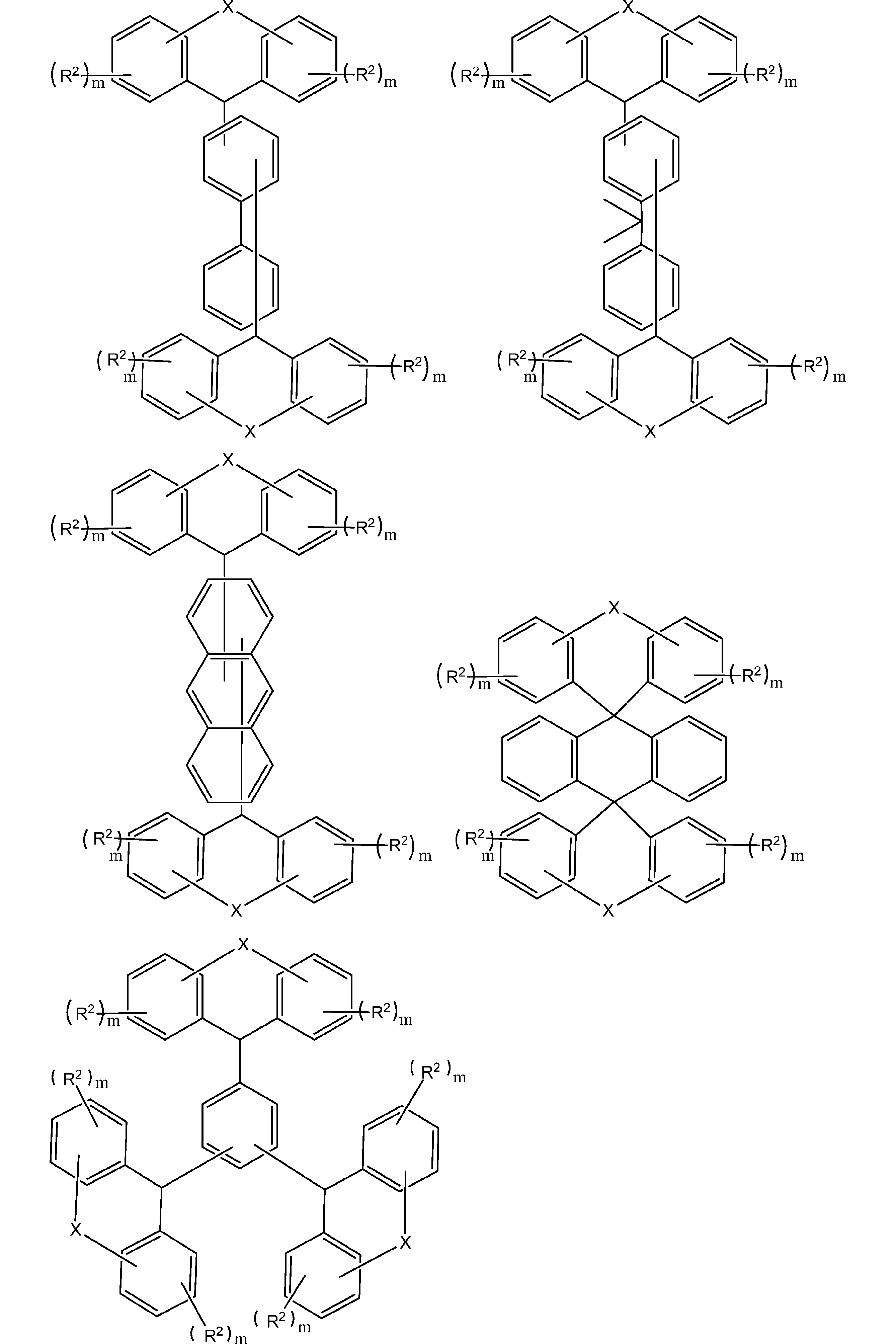

(式中、Xは、上記式(1)で説明したものと同義である。)
(In the formula, X has the same meaning as described in the above formula (1).)

(式中、Xは、上記式(1)で説明したものと同義である。)
(In the formula, X has the same meaning as described in the above formula (1).)

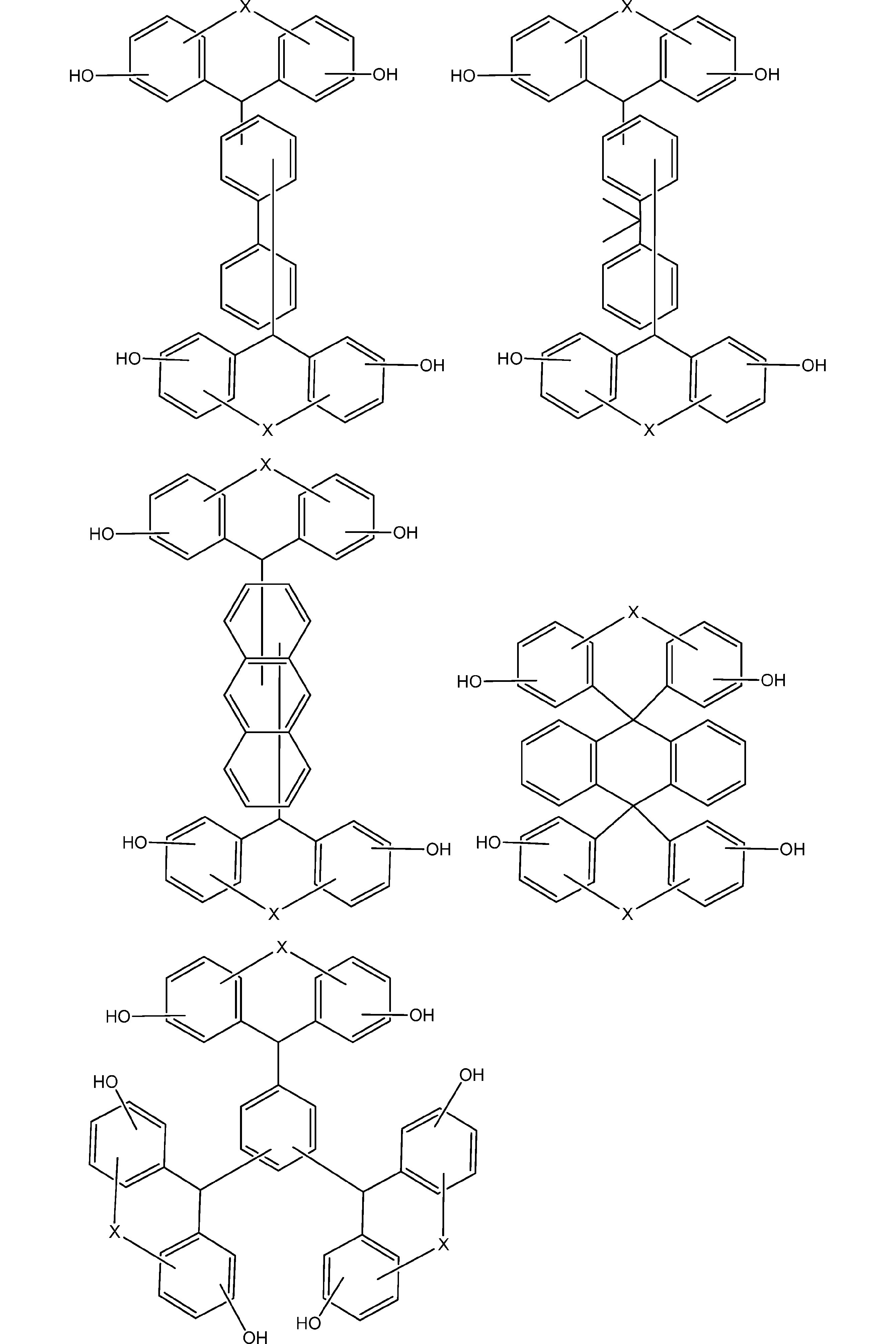

ここで、上記一般式(1)で示される化合物をノボラック化する際に用いるアルデヒドとしては、例えば、ホルムアルデヒド、トリオキサン、パラホルムアルデヒド、ベンズアルデヒド、アセトアルデヒド、プロピルアルデヒド、フェニルアセトアルデヒド、フェニルプロピルアルデヒド、ヒドロキシベンズアルデヒド、クロロベンズアルデヒド、ニトロベンズアルデヒド、メチルベンズアルデヒド、エチルベンズアルデヒド、ブチルベンズアルデヒド、ビフェニルアルデヒド、ナフトアルデヒド、アントラセンカルボアルデヒド、フェナントレンカルボアルデヒド、ピレンカルボアルデヒド、フルフラール等が挙げられるが、これらに特に限定されない。これらの中でも、ホルムアルデヒドがより好ましい。なお、これらのアルデヒド類は、1種を単独で、又は2種以上を組み合わせて用いることができる。また、上記アルデヒド類の使用量は、特に限定されないが、上記一般式(1)で示される化合物1モルに対して、0.2~5モルが好ましく、より好ましくは0.5~2モルである。 Specific examples of the resin having the structure represented by the general formula (2) include, for example, a resin in which the compound represented by the general formula (1) is novolakized by a condensation reaction with an aldehyde which is a crosslinking-reactive monomer. Is mentioned.
Here, as an aldehyde used when novolak-forming the compound represented by the general formula (1), for example, formaldehyde, trioxane, paraformaldehyde, benzaldehyde, acetaldehyde, propylaldehyde, phenylacetaldehyde, phenylpropylaldehyde, hydroxybenzaldehyde, Examples include, but are not limited to, chlorobenzaldehyde, nitrobenzaldehyde, methylbenzaldehyde, ethylbenzaldehyde, butylbenzaldehyde, biphenylaldehyde, naphthaldehyde, anthracenecarbaldehyde, phenanthrenecarbaldehyde, pyrenecarbaldehyde, and furfural. Among these, formaldehyde is more preferable. In addition, these aldehydes can be used individually by 1 type or in combination of 2 or more types. The amount of the aldehyde used is not particularly limited, but is preferably 0.2 to 5 mol, more preferably 0.5 to 2 mol, relative to 1 mol of the compound represented by the general formula (1). is there.
本実施形態のリソグラフィー用下層膜形成材料は、上述した一般式(1)で示される化合物及び/又は一般式(2)で示される構造を有する樹脂以外に、必要に応じて、架橋剤、酸発生剤、有機溶媒等の他の成分を含んでいてもよい。以下、これらの任意成分について説明する。 (Other ingredients)
The lower layer film forming material for lithography according to the present embodiment includes, in addition to the compound represented by the general formula (1) and / or the resin having the structure represented by the general formula (2), a crosslinking agent, an acid, if necessary. Other components such as a generator and an organic solvent may be included. Hereinafter, these optional components will be described.
本実施形態で使用可能な架橋剤の具体例としては、例えば、メラミン化合物、グアナミン化合物、グリコールウリル化合物、ウレア化合物、エポキシ化合物、チオエポキシ化合物、イソシアネート化合物、アジド化合物、アルケニルエーテル基などの2重結合を含む化合物であって、メチロール基、アルコキシメチル基、アシロキシメチル基から選ばれる少なくとも一つの基を置換基(架橋性基)として有するものなどが挙げるが、これらに特に限定されない。なお、これらの架橋剤は、1種を単独で、或いは2種以上を組み合わせて用いることができる。また、これらは添加剤として用いてもよい。なお、上記架橋性基を一般式(1)で示される化合物及び/又は一般式(2)で示される構造を有する樹脂におけるポリマー側鎖にペンダント基として導入してもよい。また、ヒドロキシ基を含む化合物も架橋剤として用いることができる。 The lower layer film forming material for lithography of the present embodiment may contain a crosslinking agent as necessary from the viewpoint of suppressing intermixing.
Specific examples of the crosslinking agent that can be used in this embodiment include double bonds such as melamine compounds, guanamine compounds, glycoluril compounds, urea compounds, epoxy compounds, thioepoxy compounds, isocyanate compounds, azide compounds, alkenyl ether groups, and the like. And a compound having at least one group selected from a methylol group, an alkoxymethyl group, and an acyloxymethyl group as a substituent (crosslinkable group), but is not particularly limited thereto. In addition, these crosslinking agents can be used individually by 1 type or in combination of 2 or more types. Moreover, you may use these as an additive. In addition, you may introduce | transduce the said crosslinkable group as a pendant group in the polymer side chain in the resin which has a structure shown by the compound shown by General formula (1), and / or General formula (2). A compound containing a hydroxy group can also be used as a crosslinking agent.
1)下記一般式(P1a-1)、(P1a-2)、(P1a-3)又は(P1b)のオニウム塩、
2)下記一般式(P2)のジアゾメタン誘導体、
3)下記一般式(P3)のグリオキシム誘導体、
4)下記一般式(P4)のビススルホン誘導体、
5)下記一般式(P5)のN-ヒドロキシイミド化合物のスルホン酸エステル、
6)β-ケトスルホン酸誘導体、
7)ジスルホン誘導体、
8)ニトロベンジルスルホネート誘導体、
9)スルホン酸エステル誘導体
等が挙げられるが、これらに特に限定されない。なお、これらの酸発生剤は、1種を単独で、或いは2種以上を組み合わせて用いることができる。 As an acid generator,
1) Onium salts of the following general formula (P1a-1), (P1a-2), (P1a-3) or (P1b)
2) a diazomethane derivative of the following general formula (P2),
3) a glyoxime derivative of the following general formula (P3),
4) A bissulfone derivative of the following general formula (P4),
5) A sulfonic acid ester of an N-hydroxyimide compound of the following general formula (P5),
6) β-ketosulfonic acid derivative,
7) a disulfone derivative,
8) Nitrobenzyl sulfonate derivative,
9) Examples thereof include, but are not particularly limited to, sulfonic acid ester derivatives. In addition, these acid generators can be used individually by 1 type or in combination of 2 or more types.


これらのなかでも、特に、トリフルオロメタンスルホン酸トリフェニルスルホニウム、トリフルオロメタンスルホン酸(p-tert-ブトキシフェニル)ジフェニルスルホニウム、トリフルオロメタンスルホン酸トリス(p-tert-ブトキシフェニル)スルホニウム、p-トルエンスルホン酸トリフェニルスルホニウム、p-トルエンスルホン酸(p-tert-ブトキシフェニル)ジフェニルスルホニウム、p-トルエンスルホン酸トリス(p-tert-ブトキシフェニル)スルホニウム、トリフルオロメタンスルホン酸トリナフチルスルホニウム、トリフルオロメタンスルホン酸シクロヘキシルメチル(2-オキソシクロヘキシル)スルホニウム、トリフルオロメタンスルホン酸(2-ノルボニル)メチル(2-オキソシクロヘキシル)スルホニウム、1,2’-ナフチルカルボニルメチルテトラヒドロチオフェニウムトリフレート等のオニウム塩;ビス(ベンゼンスルホニル)ジアゾメタン、ビス(p-トルエンスルホニル)ジアゾメタン、ビス(シクロヘキシルスルホニル)ジアゾメタン、ビス(n-ブチルスルホニル)ジアゾメタン、ビス(イソブチルスルホニル)ジアゾメタン、ビス(sec-ブチルスルホニル)ジアゾメタン、ビス(n-プロピルスルホニル)ジアゾメタン、ビス(イソプロピルスルホニル)ジアゾメタン、ビス(tert-ブチルスルホニル)ジアゾメタン等のジアゾメタン誘導体;ビス-(p-トルエンスルホニル)-α-ジメチルグリオキシム、ビス-(n-ブタンスルホニル)-α-ジメチルグリオキシム等のグリオキシム誘導体、ビスナフチルスルホニルメタン等のビススルホン誘導体;N-ヒドロキシスクシンイミドメタンスルホン酸エステル、N-ヒドロキシスクシンイミドトリフルオロメタンスルホン酸エステル、N-ヒドロキシスクシンイミド1-プロパンスルホン酸エステル、N-ヒドロキシスクシンイミド2-プロパンスルホン酸エステル、N-ヒドロキシスクシンイミド1-ペンタンスルホン酸エステル、N-ヒドロキシスクシンイミドp-トルエンスルホン酸エステル、N-ヒドロキシナフタルイミドメタンスルホン酸エステル、N-ヒドロキシナフタルイミドベンゼンスルホン酸エステル等のN-ヒドロキシイミド化合物のスルホン酸エステル誘導体等が好ましく用いられる。 Specific examples of the acid generator include, but are not limited to, tetramethylammonium trifluoromethanesulfonate, tetramethylammonium nonafluorobutanesulfonate, triethylammonium nonafluorobutanesulfonate, pyridinium nonafluorobutanesulfonate, camphorsulfonic acid Triethylammonium, pyridinium camphorsulfonate, tetra-n-butylammonium nonafluorobutanesulfonate, tetraphenylammonium nonafluorobutanesulfonate, tetramethylammonium p-toluenesulfonate, diphenyliodonium trifluoromethanesulfonate, trifluoromethanesulfonic acid (p -Tert-butoxyphenyl) phenyliodonium, p-toluenesulfonic acid diphenyliodoni P-toluenesulfonic acid (p-tert-butoxyphenyl) phenyliodonium, trifluoromethanesulfonic acid triphenylsulfonium, trifluoromethanesulfonic acid (p-tert-butoxyphenyl) diphenylsulfonium, trifluoromethanesulfonic acid bis (p-tert -Butoxyphenyl) phenylsulfonium, trifluoromethanesulfonic acid tris (p-tert-butoxyphenyl) sulfonium, p-toluenesulfonic acid triphenylsulfonium, p-toluenesulfonic acid (p-tert-butoxyphenyl) diphenylsulfonium, p-toluene Bis (p-tert-butoxyphenyl) sulfonic acid phenylsulfonium, Tris (p-tert-butoxyphenyl) p-toluenesulfonic acid Ruphonium, triphenylsulfonium nonafluorobutanesulfonate, triphenylsulfonium butanesulfonate, trimethylsulfonium trifluoromethanesulfonate, trimethylsulfonium p-toluenesulfonate, cyclohexylmethyl (2-oxocyclohexyl) sulfonium trifluoromethanesulfonate, p-toluene Cyclohexylmethyl (2-oxocyclohexyl) sulfonium sulfonate, dimethylphenylsulfonium trifluoromethanesulfonate, dimethylphenylsulfonium p-toluenesulfonate, dicyclohexylphenylsulfonium trifluoromethanesulfonate, dicyclohexylphenylsulfonium p-toluenesulfonate, trifluoromethanesulfonic acid Trinaphthylsulfoniu , Cyclohexylmethyl trifluoromethanesulfonate (2-oxocyclohexyl) sulfonium, trifluoromethanesulfonate (2-norbornyl) methyl (2-oxocyclohexyl) sulfonium, ethylenebis [methyl (2-oxocyclopentyl) sulfonium trifluoromethanesulfonate] Onium salts such as 1,2′-naphthylcarbonylmethyltetrahydrothiophenium triflate; bis (benzenesulfonyl) diazomethane, bis (p-toluenesulfonyl) diazomethane, bis (xylenesulfonyl) diazomethane, bis (cyclohexylsulfonyl) diazomethane, Bis (cyclopentylsulfonyl) diazomethane, bis (n-butylsulfonyl) diazomethane, bis (isobutylsulfonyl) diazomethane Bis (sec-butylsulfonyl) diazomethane, bis (n-propylsulfonyl) diazomethane, bis (isopropylsulfonyl) diazomethane, bis (tert-butylsulfonyl) diazomethane, bis (n-amylsulfonyl) diazomethane, bis (isoamylsulfonyl) diazomethane Bis (sec-amylsulfonyl) diazomethane, bis (tert-amylsulfonyl) diazomethane, 1-cyclohexylsulfonyl-1- (tert-butylsulfonyl) diazomethane, 1-cyclohexylsulfonyl-1- (tert-amylsulfonyl) diazomethane, Diazomethane derivatives such as tert-amylsulfonyl-1- (tert-butylsulfonyl) diazomethane; bis- (p-toluenesulfonyl) -α-dimethyl Lioxime, bis- (p-toluenesulfonyl) -α-diphenylglyoxime, bis- (p-toluenesulfonyl) -α-dicyclohexylglyoxime, bis- (p-toluenesulfonyl) -2,3-pentanedione glyoxime, Bis- (p-toluenesulfonyl) -2-methyl-3,4-pentanedione glyoxime, bis- (n-butanesulfonyl) -α-dimethylglyoxime, bis- (n-butanesulfonyl) -α-diphenylglyoxime Oxime, bis- (n-butanesulfonyl) -α-dicyclohexylglyoxime, bis- (n-butanesulfonyl) -2,3-pentanedione glyoxime, bis- (n-butanesulfonyl) -2-methyl-3, 4-Pentanedione glyoxime, bis- (methanesulfonyl) -α-dimethylglio Xime, bis- (trifluoromethanesulfonyl) -α-dimethylglyoxime, bis- (1,1,1-trifluoroethanesulfonyl) -α-dimethylglyoxime, bis- (tert-butanesulfonyl) -α-dimethylglyoxime Oxime, bis- (perfluorooctanesulfonyl) -α-dimethylglyoxime, bis- (cyclohexanesulfonyl) -α-dimethylglyoxime, bis- (benzenesulfonyl) -α-dimethylglyoxime, bis- (p-fluorobenzene) Sulfonyl) -α-dimethylglyoxime, bis- (p-tert-butylbenzenesulfonyl) -α-dimethylglyoxime, bis- (xylenesulfonyl) -α-dimethylglyoxime, bis- (camphorsulfonyl) -α-dimethyl Glyoxy such as glyoxime Derivatives; bissulfone derivatives such as bisnaphthylsulfonylmethane, bistrifluoromethylsulfonylmethane, bismethylsulfonylmethane, bisethylsulfonylmethane, bispropylsulfonylmethane, bisisopropylsulfonylmethane, bis-p-toluenesulfonylmethane, bisbenzenesulfonylmethane; Β-ketosulfone derivatives such as 2-cyclohexylcarbonyl-2- (p-toluenesulfonyl) propane and 2-isopropylcarbonyl-2- (p-toluenesulfonyl) propane; disulfone derivatives such as diphenyldisulfone derivatives and dicyclohexyldisulfone derivatives, p- Nitrobenzyl sulfonate derivatives such as 2,6-dinitrobenzyl toluenesulfonate and 2,4-dinitrobenzyl p-toluenesulfonate; 1 Sulfonic acid ester derivatives such as 2,3-tris (methanesulfonyloxy) benzene, 1,2,3-tris (trifluoromethanesulfonyloxy) benzene, 1,2,3-tris (p-toluenesulfonyloxy) benzene; N -Hydroxysuccinimide methanesulfonate ester, N-hydroxysuccinimide trifluoromethanesulfonate ester, N-hydroxysuccinimide ethanesulfonate ester, N-hydroxysuccinimide 1-propanesulfonate ester, N-hydroxysuccinimide 2-propanesulfonate ester, N -Hydroxysuccinimide 1-pentanesulfonate, N-hydroxysuccinimide 1-octanesulfonate, N-hydroxysuccinimide p-toluenesulfo Acid ester, N-hydroxysuccinimide p-methoxybenzenesulfonate, N-hydroxysuccinimide 2-chloroethanesulfonate, N-hydroxysuccinimidebenzenesulfonate, N-hydroxysuccinimide-2,4,6-trimethylbenzenesulfonate Ester, N-hydroxysuccinimide 1-naphthalene sulfonate, N-hydroxy succinimide 2-naphthalene sulfonate, N-hydroxy-2-phenylsuccinimide methane sulfonate, N-hydroxy maleimide methane sulfonate, N-hydroxy maleimide Ethanesulfonic acid ester, N-hydroxy-2-phenylmaleimide methanesulfonic acid ester, N-hydroxyglutarimide Tansulfonic acid ester, N-hydroxyglutarimide benzenesulfonic acid ester, N-hydroxyphthalimide methanesulfonic acid ester, N-hydroxyphthalimide benzenesulfonic acid ester, N-hydroxyphthalimide trifluoromethanesulfonic acid ester, N-hydroxyphthalimide p-toluene Sulfonic acid ester, N-hydroxynaphthalimide methanesulfonic acid ester, N-hydroxynaphthalimide benzenesulfonic acid ester, N-hydroxy-5-norbornene-2,3-dicarboximide methanesulfonic acid ester, N-hydroxy-5- Norbornene-2,3-dicarboximide trifluoromethanesulfonate, N-hydroxy-5-norbornene-2,3-dicarboximide p- Sulfonic acid ester derivatives of N- hydroxy imide compounds such as toluene sulfonic acid esters.
Among these, in particular, triphenylsulfonium trifluoromethanesulfonate, trifluoromethanesulfonic acid (p-tert-butoxyphenyl) diphenylsulfonium, trifluoromethanesulfonic acid tris (p-tert-butoxyphenyl) sulfonium, p-toluenesulfonic acid Triphenylsulfonium, p-toluenesulfonic acid (p-tert-butoxyphenyl) diphenylsulfonium, p-toluenesulfonic acid tris (p-tert-butoxyphenyl) sulfonium, trifluoromethanesulfonic acid trinaphthylsulfonium, trifluoromethanesulfonic acid cyclohexylmethyl (2-oxocyclohexyl) sulfonium, trifluoromethanesulfonic acid (2-norbornyl) methyl (2-oxocyclohexyl) Sil) sulfonium, onium salts such as 1,2'-naphthylcarbonylmethyltetrahydrothiophenium triflate; bis (benzenesulfonyl) diazomethane, bis (p-toluenesulfonyl) diazomethane, bis (cyclohexylsulfonyl) diazomethane, bis (n- Diazomethane derivatives such as butylsulfonyl) diazomethane, bis (isobutylsulfonyl) diazomethane, bis (sec-butylsulfonyl) diazomethane, bis (n-propylsulfonyl) diazomethane, bis (isopropylsulfonyl) diazomethane, bis (tert-butylsulfonyl) diazomethane; Glyoxime derivatives such as bis- (p-toluenesulfonyl) -α-dimethylglyoxime and bis- (n-butanesulfonyl) -α-dimethylglyoxime; Bissulfone derivatives such as naphthylsulfonylmethane; N-hydroxysuccinimide methanesulfonate, N-hydroxysuccinimide trifluoromethanesulfonate, N-hydroxysuccinimide 1-propanesulfonate, N-hydroxysuccinimide 2-propanesulfonate, N-hydroxysuccinimide 1-pentanesulfonic acid ester, N-hydroxysuccinimide p-toluenesulfonic acid ester, N-hydroxynaphthalimide methanesulfonic acid ester, N-hydroxynaphthalimide benzenesulfonic acid ester, etc. Acid ester derivatives and the like are preferably used.
有機溶媒の具体例としては、アセトン、メチルエチルケトン、メチルイソブチルケトン、シクロヘキサノン等のケトン系溶媒;プロピレングリコールモノメチルエーテル、プロピレングリコールモノメチルエーテルアセテート等のセロソルブ系溶媒;乳酸エチル、酢酸メチル、酢酸エチル、酢酸ブチル、酢酸イソアミル、乳酸エチル、メトキシプロピオン酸メチル、ヒドロキシイソ酪酸メチル等のエステル系溶媒;メタノール、エタノール、イソプロパノール、1-エトキシ-2-プロパノール等のアルコール系溶媒;トルエン、キシレン、アニソール等の芳香族系炭化水素等が挙げられるが、これらに特に限定されない。これらの有機溶媒は、1種を単独で、或いは2種以上を組み合わせて用いることができる。 The material for forming a lower layer film for lithography of the present embodiment may contain an organic solvent. Any known organic solvent can be used as long as it dissolves at least the compound represented by the general formula (1) and / or the resin having the structure represented by the general formula (2).
Specific examples of organic solvents include ketone solvents such as acetone, methyl ethyl ketone, methyl isobutyl ketone, and cyclohexanone; cellosolv solvents such as propylene glycol monomethyl ether and propylene glycol monomethyl ether acetate; ethyl lactate, methyl acetate, ethyl acetate, butyl acetate Ester solvents such as isoamyl acetate, ethyl lactate, methyl methoxypropionate and methyl hydroxyisobutyrate; alcohol solvents such as methanol, ethanol, isopropanol and 1-ethoxy-2-propanol; aromatics such as toluene, xylene and anisole Examples thereof include, but are not limited to, hydrocarbons. These organic solvents can be used individually by 1 type or in combination of 2 or more types.
本実施形態のリソグラフィー用下層膜は、本実施形態のリソグラフィー用下層膜形成材料から形成される。 [Liquid lower layer film and multilayer resist pattern forming method]
The lower layer film for lithography of this embodiment is formed from the lower layer film forming material for lithography of this embodiment.
このような中間層膜の上に直接フォトレジスト膜を形成することができるが、中間層膜の上に有機反射防止膜(BARC)をスピンコートで形成して、その上にフォトレジスト膜を形成してもよい。 Here, when an inorganic hard mask intermediate layer film is formed as the intermediate layer, a silicon oxide film, a silicon nitride film, or a silicon oxynitride film (SiON film) is formed by a CVD method, an ALD method, or the like. The method for forming the nitride film is not limited to the following, but for example, a method described in Japanese Patent Application Laid-Open No. 2002-334869 (Patent Document 6) and WO 2004/066377 (Patent Document 7) can be used.
A photoresist film can be formed directly on such an intermediate film, but an organic antireflection film (BARC) is formed on the intermediate film by spin coating, and a photoresist film is formed thereon. May be.
なお、基板は、公知のものを適宜選択して使用することができ、特に限定されないが、Si、α-Si、p-Si、SiO2、SiN、SiON、W、TiN、Al等が挙げられる。また、基板は、基材(支持体)上に被加工膜(被加工基板)を有する積層体であってもよい。このような被加工膜としては、Si、SiO2、SiON、SiN、p-Si、α-Si、W、W-Si、Al、Cu、Al-Si等種々のLow-k膜及びそのストッパー膜等が挙げられ、通常、基材(支持体)とは異なる材質のものが用いられる。なお、加工対象となる基板或いは被加工膜の厚さは、特に限定されないが、通常、50~10,000nm程度であることが好ましく、より好ましくは75~5,000nmである。 The lower layer film of this embodiment is characterized by excellent etching resistance of these substrates.
A known substrate can be appropriately selected and used, and is not particularly limited. Examples thereof include Si, α-Si, p-Si, SiO 2 , SiN, SiON, W, TiN, and Al. . The substrate may be a laminate having a film to be processed (substrate to be processed) on a base material (support). Examples of such processed films include various low-k films such as Si, SiO 2 , SiON, SiN, p-Si, α-Si, W, W-Si, Al, Cu, and Al-Si, and their stopper films. In general, a material different from the base material (support) is used. The thickness of the substrate to be processed or the film to be processed is not particularly limited, but is usually preferably about 50 to 10,000 nm, more preferably 75 to 5,000 nm.
有機元素分析により炭素濃度及び酸素濃度(質量%)を測定した。
装置:CHNコーダーMT-6(ヤナコ分析工業(株)製)
(分子量)
GC-MS分析により、Agilent社製Agilent5975/6890Nを用いて測定した。あるいは、LC-MS分析により、Water社製Acquity UPLC/MALDI-Synapt HDMSを用いて測定した。
(ポリスチレン換算分子量)
ゲル浸透クロマトグラフィー(GPC)分析により、ポリスチレン換算の重量平均分子量(Mw)、数平均分子量(Mn)を求め、分散度(Mw/Mn)を求めた。
装置:Shodex GPC-101型(昭和電工(株)製)
カラム:KF-80M×3
溶離液:THF 1ml/min
温度:40℃
(熱分解温度(Tg))
エスアイアイ・ナノテクノロジー社製EXSTAR6000DSC装置を使用し、試料約5mgをアルミニウム製非密封容器に入れ、窒素ガス(30ml/min)気流中昇温速度10℃/minで500℃まで昇温した。その際、ベースラインに減少部分が現れる温度を熱分解温度(Tg)とした。
(溶解度)
23℃にて、化合物の1-メトキシ-2-プロパノール(PGME)及びプロピレングリコールモノメチルエーテルアセテート(PGMEA)に対する溶解量を測定し、その結果を以下の基準で評価した。
評価A:10wt%以上
評価B:3wt%以上10wt%未満
評価C:3wt%未満 (Carbon concentration and oxygen concentration)
Carbon concentration and oxygen concentration (mass%) were measured by organic elemental analysis.
Apparatus: CHN coder MT-6 (manufactured by Yanaco Analytical Co., Ltd.)
(Molecular weight)
By GC-MS analysis, measurement was performed using Agilent 5975 / 6890N manufactured by Agilent. Alternatively, measurement was performed by LC-MS analysis using Water UP Acquity UPLC / MALDI-Synapt HDMS.
(Molecular weight in terms of polystyrene)
The weight average molecular weight (Mw) and number average molecular weight (Mn) in terms of polystyrene were determined by gel permeation chromatography (GPC) analysis, and the degree of dispersion (Mw / Mn) was determined.
Apparatus: Shodex GPC-101 (manufactured by Showa Denko KK)
Column: KF-80M x 3
Eluent: THF 1ml / min
Temperature: 40 ° C
(Thermal decomposition temperature (Tg))
Using an EXSTAR6000DSC apparatus manufactured by SII Nanotechnology Inc., about 5 mg of a sample was placed in an aluminum non-sealed container and heated to 500 ° C. at a temperature rising rate of 10 ° C./min in a nitrogen gas (30 ml / min) air stream. At that time, the temperature at which the decreased portion appeared in the baseline was defined as the thermal decomposition temperature (Tg).
(solubility)
The amount of the compound dissolved in 1-methoxy-2-propanol (PGME) and propylene glycol monomethyl ether acetate (PGMEA) was measured at 23 ° C., and the results were evaluated according to the following criteria.
Evaluation A: 10 wt% or more Evaluation B: 3 wt% or more and less than 10 wt% Evaluation C: Less than 3 wt%
攪拌機、冷却管及びビュレットを備えた内容積100mlの容器を準備した。この容器に、ハイドロキノン(シグマ-アルドリッチ社製試薬)1.10g(10mmol)と、4-ビフェニルアルデヒド(三菱瓦斯化学社製)1.82g(10mmol)と、メチルイソブチルケトン30mlとを仕込み、95%の硫酸5mlを加えて、反応液を調製した。この反応液を100℃で6時間撹拌して反応を行った。次に、反応液を濃縮し、純水50gを加えて反応生成物を析出させ、室温まで冷却した後、濾過を行って分離した。濾過により得られた固形物を乾燥させた後、カラムクロマトによる分離精製を行うことにより、下記式で示される目的化合物(BisP-1)1.05gを得た。
なお、400MHz-1H-NMRにより以下のピークが見出され、下記式の化学構造を有することを確認した。
1H-NMR:(d-DMSO、内部標準TMS)
δ(ppm)9.6(2H,O-H)、7.2~8.3(15H,Ph-H)、6.6(1H,C-H) (Synthesis Example 1) Synthesis of BisP-1 A container having an internal volume of 100 ml equipped with a stirrer, a cooling tube and a burette was prepared. In this container, 1.10 g (10 mmol) of hydroquinone (reagent manufactured by Sigma-Aldrich), 1.82 g (10 mmol) of 4-biphenylaldehyde (manufactured by Mitsubishi Gas Chemical Company), and 30 ml of methyl isobutyl ketone were charged, and 95% Of 5 ml of sulfuric acid was added to prepare a reaction solution. The reaction was stirred at 100 ° C. for 6 hours to carry out the reaction. Next, the reaction solution was concentrated, and 50 g of pure water was added to precipitate the reaction product. After cooling to room temperature, the solution was filtered and separated. The solid obtained by filtration was dried and then separated and purified by column chromatography to obtain 1.05 g of the target compound (BisP-1) represented by the following formula.
The following peaks were found by 400 MHz- 1 H-NMR, and confirmed to have a chemical structure of the following formula.
1 H-NMR: (d-DMSO, internal standard TMS)
δ (ppm) 9.6 (2H, OH), 7.2 to 8.3 (15H, Ph—H), 6.6 (1H, C—H)

得られた化合物について、前記方法により分子量を測定した結果、366であった。
熱重量測定(TG)の結果、得られた化合物(BisP-1)の熱分解温度は350℃以上であった。そのため、高い耐熱性を有し、高温ベークへの適用が可能であるものと評価された。
PGME及びPGMEAへの溶解性を評価した結果、20wt%以上(評価A)であり、化合物(BisP-1)は優れた溶解性を有するものと評価された。そのため、化合物(BisP-1)は溶液状態で高い保存安定性を有し、半導体微細加工プロセスで広く用いられるエッジビートリンス液(PGME/PGMEA混合液)にも十分に適用できるものと評価された。 As a result of organic elemental analysis, the obtained compound (BisP-1) had a carbon concentration of 82.0% and an oxygen concentration of 13.0%. Since the carbon content was high and the oxygen content was low, the compound (BisP-1) was evaluated as having high etching resistance.
It was 366 as a result of measuring molecular weight by the said method about the obtained compound.
As a result of thermogravimetry (TG), the thermal decomposition temperature of the obtained compound (BisP-1) was 350 ° C. or higher. Therefore, it was evaluated that it has high heat resistance and can be applied to high temperature baking.
As a result of evaluating the solubility in PGMEA and PGMEA, it was 20 wt% or more (Evaluation A), and the compound (BisP-1) was evaluated as having excellent solubility. Therefore, it was evaluated that the compound (BisP-1) has high storage stability in a solution state and can be sufficiently applied to an edge beat rinse liquid (PGME / PGMEA mixed liquid) widely used in a semiconductor microfabrication process. .
ジムロート冷却管、温度計及び攪拌翼を備えた、底抜きが可能な内容積10Lの四つ口フラスコを準備した。この四つ口フラスコに、窒素気流中、1,5-ジメチルナフタレン1.09kg(7mol、三菱ガス化学(株)製)、40質量%ホルマリン水溶液2.1kg(ホルムアルデヒドとして28mol、三菱ガス化学(株)製)及び98質量%硫酸(関東化学(株)製)0.97mlを仕込み、常圧下、100℃で還流させながら7時間反応させた。その後、希釈溶媒としてエチルベンゼン(和光純薬工業(株)製試薬特級)1.8kgを反応液に加え、静置後、下相の水相を除去した。さらに、中和及び水洗を行い、エチルベンゼン及び未反応の1,5-ジメチルナフタレンを減圧下で留去することにより、淡褐色固体のジメチルナフタレンホルムアルデヒド樹脂1.25kgを得た。
得られたジメチルナフタレンホルムアルデヒドの分子量は、Mn:562、Mw:1168、Mw/Mn:2.08であった。また、炭素濃度は84.2質量%、酸素濃度は8.3質量%であった。 (Production Example 1)
A four-necked flask with an internal volume of 10 L capable of bottoming was prepared, equipped with a Dimroth condenser, thermometer, and stirring blade. To this four-necked flask, in a nitrogen stream, 1.09 kg of 1,5-dimethylnaphthalene (7 mol, manufactured by Mitsubishi Gas Chemical Co., Ltd.), 2.1 kg of 40% by weight formalin aqueous solution (28 mol of formaldehyde, Mitsubishi Gas Chemical Co., Ltd.) )) And 98 mass% sulfuric acid (manufactured by Kanto Chemical Co., Ltd.) 0.97 ml were charged and reacted for 7 hours under reflux at 100 ° C. under normal pressure. Thereafter, 1.8 kg of ethylbenzene (special grade reagent manufactured by Wako Pure Chemical Industries, Ltd.) as a diluent solvent was added to the reaction solution, and after standing, the lower aqueous phase was removed. Further, neutralization and washing with water were carried out, and ethylbenzene and unreacted 1,5-dimethylnaphthalene were distilled off under reduced pressure to obtain 1.25 kg of a light brown solid dimethylnaphthalene formaldehyde resin.
The molecular weight of the obtained dimethylnaphthalene formaldehyde was Mn: 562, Mw: 1168, Mw / Mn: 2.08. Moreover, carbon concentration was 84.2 mass% and oxygen concentration was 8.3 mass%.
得られた樹脂(CR-1)は、Mn:885、Mw:2220、Mw/Mn:4.17であった。また、炭素濃度は89.1質量%、酸素濃度は4.5質量%であった。 Subsequently, a four-necked flask having an internal volume of 0.5 L equipped with a Dimroth condenser, a thermometer, and a stirring blade was prepared. This four-necked flask was charged with 100 g (0.51 mol) of the dimethylnaphthalene formaldehyde resin obtained as described above and 0.05 g of paratoluenesulfonic acid under a nitrogen stream, and the temperature was raised to 190 ° C. Stir after heating for hours. Thereafter, 52.0 g (0.36 mol) of 1-naphthol was further added, and the temperature was further raised to 220 ° C. to react for 2 hours. After the solvent was diluted, neutralization and water washing were performed, and the solvent was removed under reduced pressure to obtain 126.1 g of a dark brown solid modified resin (CR-1).
The obtained resin (CR-1) was Mn: 885, Mw: 2220, and Mw / Mn: 4.17. The carbon concentration was 89.1% by mass, and the oxygen concentration was 4.5% by mass.
表1に示す組成となるように、実施例1、比較例1に対応するリソグラフィー用下層膜形成材料を各々調製した。すなわち、下記の材料を使用した。
酸発生剤:みどり化学社製 ジターシャリーブチルジフェニルヨードニウムノナフルオロメタンスルホナート(DTDPI)
架橋剤:三和ケミカル社製 ニカラックMX270(ニカラック)
有機溶媒:シクロヘキサノン(CHN)
ノボラック:群栄化学社製 PSM4357
次に、実施例1、比較例1の下層膜形成材料をシリコン基板上に回転塗布し、その後、240℃で60秒間、さらに400℃で120秒間ベークして、膜厚200nmの下層膜を各々作製した。
そして、下記に示す条件でエッチング試験を行い、エッチング耐性を評価した。評価結果を表1に示す。 <Example 1, comparative example 1>
Lithographic lower layer film forming materials corresponding to Example 1 and Comparative Example 1 were prepared so as to have the compositions shown in Table 1, respectively. That is, the following materials were used.
Acid generator: Ditertiary butyl diphenyliodonium nonafluoromethanesulfonate (DTDPI) manufactured by Midori Chemical Co., Ltd.
Cross-linking agent: Nikalac MX270 (Nikalac) manufactured by Sanwa Chemical Co., Ltd.
Organic solvent: cyclohexanone (CHN)
Novolak: PSM4357 manufactured by Gunei Chemical Co., Ltd.
Next, the lower layer film-forming materials of Example 1 and Comparative Example 1 were spin-coated on a silicon substrate, and then baked at 240 ° C. for 60 seconds and further at 400 ° C. for 120 seconds to form 200 nm-thick lower layer films. Produced.
And the etching test was done on the conditions shown below, and etching tolerance was evaluated. The evaluation results are shown in Table 1.
エッチング装置:サムコインターナショナル社製 RIE-10NR
出力:50W
圧力:20Pa
時間:2min
エッチングガス
Arガス流量:CF4ガス流量:O2ガス流量=50:5:5(sccm)
[エッチング耐性の評価]
エッチング耐性の評価は、以下の手順で行った。
まず、実施例1の化合物(BisP-1)に代えてノボラック(群栄化学社製 PSM4357)を用いること以外は、実施例1と同様の条件で、ノボラックの下層膜を作製した。そして、このノボラックの下層膜を対象として、上記のエッチング試験を行い、そのときのエッチングレートを測定した。
次に、実施例1及び比較例1の下層膜を対象として、上記エッチング試験を同様に行い、そのときのエッチングレートを測定した。
そして、ノボラックの下層膜のエッチングレートを基準として、以下の評価基準でエッチング耐性を評価した。
<評価基準>
A:ノボラックの下層膜に比べてエッチングレートが、-10%未満
B:ノボラックの下層膜に比べてエッチングレートが、-10%~+5%
C:ノボラックの下層膜に比べてエッチングレートが、+5%超 [Etching test]
Etching device: RIE-10NR manufactured by Samco International
Output: 50W
Pressure: 20Pa
Time: 2min
Etching gas Ar gas flow rate: CF 4 gas flow rate: O 2 gas flow rate = 50: 5: 5 (sccm)
[Evaluation of etching resistance]
Etching resistance was evaluated according to the following procedure.
First, a novolac underlayer film was produced under the same conditions as in Example 1 except that novolak (PSM4357 manufactured by Gunei Chemical Co., Ltd.) was used instead of the compound (BisP-1) in Example 1. Then, the above-described etching test was performed on this novolac lower layer film, and the etching rate at that time was measured.
Next, the above-mentioned etching test was similarly performed for the lower layer films of Example 1 and Comparative Example 1, and the etching rate at that time was measured.
Then, the etching resistance was evaluated according to the following evaluation criteria based on the etching rate of the novolak underlayer film.
<Evaluation criteria>
A: Etching rate is less than -10% compared to the novolac lower layer film B: Etching rate is -10% to + 5% compared to the novolac lower layer film
C: Etching rate is more than + 5% compared to the novolak underlayer
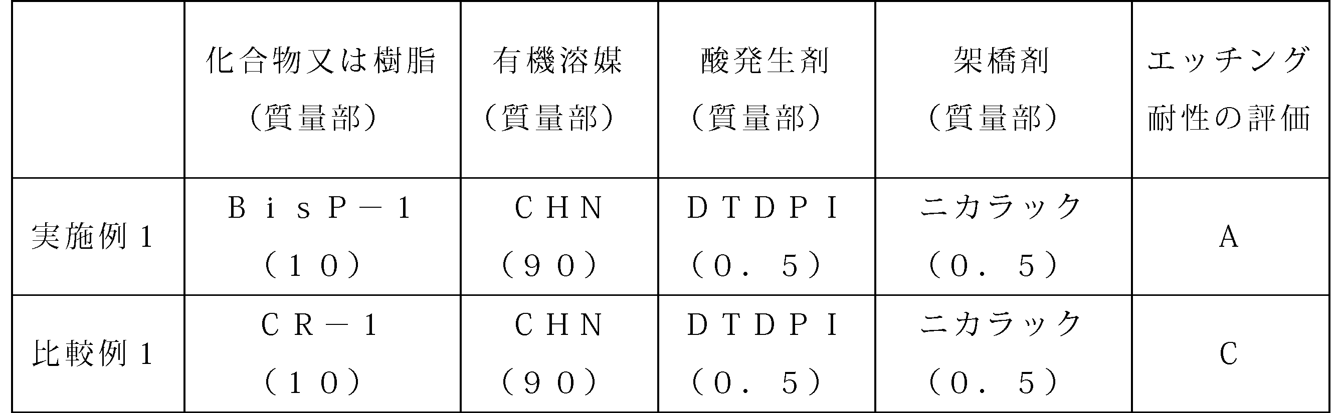
次に、実施例1のリソグラフィー用下層膜形成材料の溶液を膜厚300nmのSiO2基板上に塗布して、240℃で60秒間、さらに400℃で120秒間ベークすることにより、膜厚80nmの下層膜を各々形成した。この下層膜上に、ArF用レジスト溶液を塗布し、130℃で60秒間ベークすることにより、膜厚150nmのフォトレジスト層を形成した。なお、ArFレジスト溶液としては、下記式(11)の化合物:5質量部、トリフェニルスルホニウムノナフルオロメタンスルホナート:1質量部、トリブチルアミン:2質量部、及びPGMEA:92質量部を配合して調製したものを用いた。
なお、下記式(11)の化合物は、次のように調製した。すなわち、2-メチル-2-メタクリロイルオキシアダマンタン4.15g、メタクリルロイルオキシ-γ-ブチロラクトン3.00g、3-ヒドロキシ-1-アダマンチルメタクリレート2.08g、アゾビスイソブチロニトリル0.38gを、テトラヒドロフラン80mLに溶解させて反応溶液とした。この反応溶液を、窒素雰囲気下、反応温度を63℃に保持して、22時間重合させた後、反応溶液を400mLのn-ヘキサン中に滴下した。このようにして得られる生成樹脂を凝固精製させ、生成した白色粉末をろ過し、減圧下40℃で一晩乾燥させて下記式(11)の化合物を得た。 <Example 2>
Next, the lower layer film forming material solution for lithography of Example 1 was applied onto a 300 nm thick SiO 2 substrate, and baked at 240 ° C. for 60 seconds and further at 400 ° C. for 120 seconds, whereby a film thickness of 80 nm was obtained. Each lower layer film was formed. On this lower layer film, an ArF resist solution was applied and baked at 130 ° C. for 60 seconds to form a 150 nm-thick photoresist layer. As the ArF resist solution, a compound of the following formula (11): 5 parts by mass, triphenylsulfonium nonafluoromethanesulfonate: 1 part by mass, tributylamine: 2 parts by mass, and PGMEA: 92 parts by mass are blended. The prepared one was used.
In addition, the compound of following formula (11) was prepared as follows. That is, 4.15 g of 2-methyl-2-methacryloyloxyadamantane, 3.00 g of methacryloyloxy-γ-butyrolactone, 2.08 g of 3-hydroxy-1-adamantyl methacrylate, 0.38 g of azobisisobutyronitrile, The reaction solution was dissolved in 80 mL. This reaction solution was polymerized for 22 hours under a nitrogen atmosphere while maintaining the reaction temperature at 63 ° C., and then the reaction solution was dropped into 400 mL of n-hexane. The product resin thus obtained was coagulated and purified, and the resulting white powder was filtered and dried overnight at 40 ° C. under reduced pressure to obtain a compound of the following formula (11).

下層膜の形成を行わないこと以外は、実施例2と同様にして、フォトレジスト層をSiO2基板上に直接形成し、ポジ型のレジストパターンを得た。 <Comparative example 2>
A photoresist layer was directly formed on the SiO 2 substrate in the same manner as in Example 2 except that the lower layer film was not formed, and a positive resist pattern was obtained.
実施例2及び比較例2のそれぞれについて、得られた55nmL/S(1:1)及び80nmL/S(1:1)のレジストパターンの形状を(株)日立製作所製電子顕微鏡(S-4800)を用いて観察した。現像後のレジストパターンの形状については、パターン倒れがなく、矩形性が良好なものを良好とし、そうでないものを不良として評価した。また、当該観察の結果、パターン倒れが無く、矩形性が良好な最小の線幅を解像性として評価の指標とした。さらに、良好なパターン形状を描画可能な最小の電子線エネルギー量を感度として、評価の指標とした。その結果を、表2に示す。 [Evaluation]
For each of Example 2 and Comparative Example 2, the resist patterns of 55 nm L / S (1: 1) and 80 nm L / S (1: 1) obtained were obtained by using an electron microscope (S-4800) manufactured by Hitachi, Ltd. Was observed. As for the shape of the resist pattern after development, the resist pattern was not collapsed and the rectangular shape was good, and the resist pattern was evaluated as bad. As a result of the observation, the minimum line width with no pattern collapse and good rectangularity was used as an evaluation index as the resolution. Furthermore, the minimum amount of electron beam energy that can draw a good pattern shape is used as an evaluation index as sensitivity. The results are shown in Table 2.
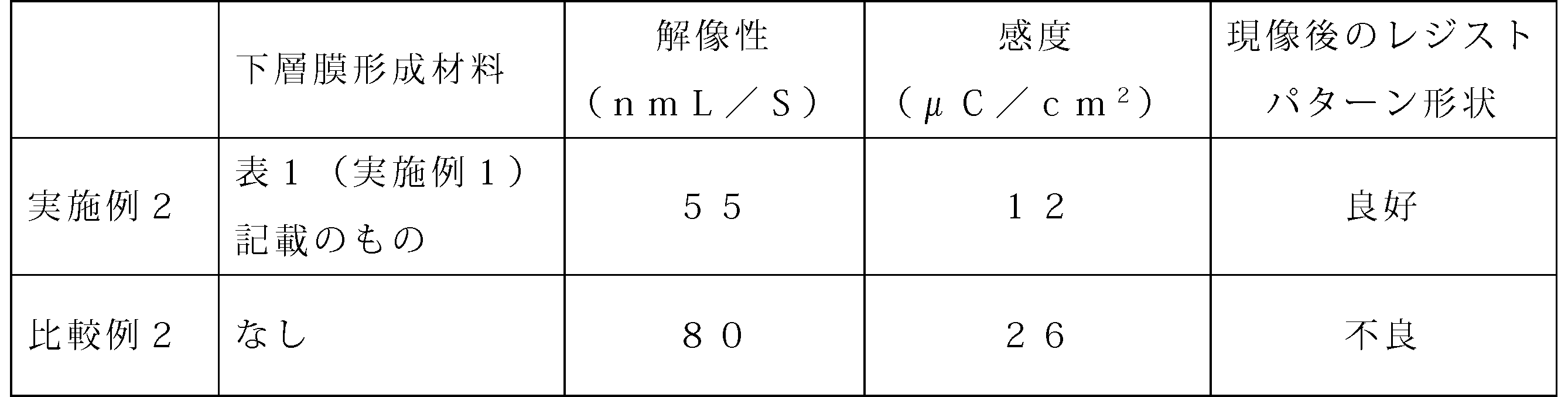
実施例1のリソグラフィー用下層膜形成材料の溶液を膜厚300nmのSiO2基板上に塗布した。次いで、240℃で60秒間、さらに400℃で120秒間ベークすることにより、膜厚80nmの下層膜を形成した。この下層膜上に、珪素含有中間層材料を塗布し、200℃で60秒間ベークすることにより、膜厚35nmの中間層膜を形成した。さらに、この中間層膜上に、実施例2で用いたArF用レジスト溶液を塗布し、130℃で60秒間ベークすることにより、膜厚150nmのフォトレジスト層を形成した。なお、珪素含有中間層材料としては、特開2007-226170号公報<合成例1>に記載の珪素原子含有ポリマーを用いた。
次いで、電子線描画装置(エリオニクス社製;ELS-7500,50keV)を用いて、フォトレジスト層を露光し、115℃で90秒間ベーク(PEB)し、2.38質量%テトラメチルアンモニウムヒドロキシド(TMAH)水溶液で60秒間現像することにより、55nmL/S(1:1)のポジ型のレジストパターンを得た。
その後、サムコインターナショナル社製 RIE-10NRを用いて、得られたレジストパターンをマスクにして珪素含有中間層膜(SOG)のドライエッチング加工を行った。続いて、得られた珪素含有中間層膜パターンをマスクにした下層膜のドライエッチング加工と、得られた下層膜パターンをマスクにしたSiO2膜のドライエッチング加工とを順次行った。 <Example 3>
The solution of the lower layer film forming material for lithography of Example 1 was applied onto a 300 nm thick SiO 2 substrate. Next, an underlayer film having a thickness of 80 nm was formed by baking at 240 ° C. for 60 seconds and further at 400 ° C. for 120 seconds. On this lower layer film, a silicon-containing intermediate layer material was applied and baked at 200 ° C. for 60 seconds to form an intermediate layer film having a thickness of 35 nm. Further, the ArF resist solution used in Example 2 was applied on the intermediate layer film, and baked at 130 ° C. for 60 seconds to form a 150 nm-thick photoresist layer. As the silicon-containing intermediate layer material, a silicon atom-containing polymer described in JP-A-2007-226170 <Synthesis Example 1> was used.
Next, the photoresist layer was exposed using an electron beam drawing apparatus (ELIONX, ELS-7500, 50 keV), baked at 115 ° C. for 90 seconds (PEB), and 2.38 mass% tetramethylammonium hydroxide ( A positive resist pattern of 55 nm L / S (1: 1) was obtained by developing with an aqueous solution of TMAH for 60 seconds.
Thereafter, dry etching of the silicon-containing intermediate layer film (SOG) was performed using RIE-10NR manufactured by Samco International Co., Ltd. using the obtained resist pattern as a mask. Subsequently, dry etching processing of the lower layer film using the obtained silicon-containing intermediate layer film pattern as a mask and dry etching processing of the SiO 2 film using the obtained lower layer film pattern as a mask were sequentially performed.
レジストパターンのレジスト中間層膜へのエッチング条件
出力:50W
圧力:20Pa
時間:1min
エッチングガス
Arガス流量:CF4ガス流量:O2ガス流量=50:8:2(sccm)
レジスト中間膜パターンのレジスト下層膜へのエッチング条件
出力:50W
圧力:20Pa
時間:2min
エッチングガス
Arガス流量:CF4ガス流量:O2ガス流量=50:5:5(sccm)
レジスト下層膜パターンのSiO 2 膜へのエッチング条件
出力:50W
圧力:20Pa
時間:2min
エッチングガス
Arガス流量:C5F12ガス流量:C2F6ガス流量:O2ガス流量
=50:4:3:1(sccm) Each etching condition is as shown below.
Etching condition output to resist intermediate layer film of resist pattern : 50W
Pressure: 20Pa
Time: 1 min
Etching gas Ar gas flow rate: CF 4 gas flow rate: O 2 gas flow rate = 50: 8: 2 (sccm)
Output of etching condition to resist underlayer film of resist intermediate film pattern : 50W
Pressure: 20Pa
Time: 2min
Etching gas Ar gas flow rate: CF 4 gas flow rate: O 2 gas flow rate = 50: 5: 5 (sccm)
Etching condition output to SiO 2 film of resist underlayer film pattern : 50W
Pressure: 20Pa
Time: 2min
Etching gas Ar gas flow rate: C 5 F 12 gas flow rate: C 2 F 6 gas flow rate: O 2 gas flow rate = 50: 4: 3: 1 (sccm)
上記のようにして得られた実施例3のパターン断面(エッチング後のSiO2膜の形状)を、(株)日立製作所製電子顕微鏡(S-4800)を用いて観察した。その結果、多層レジスト加工におけるエッチング後のSiO2膜の形状は矩形であり、欠陥も認められず、本発明の下層膜を用いた実施例3は、パターン断面においても良好な形状を有することが確認された。 [Evaluation]
The pattern cross section (shape of the SiO 2 film after etching) of Example 3 obtained as described above was observed using an electron microscope (S-4800) manufactured by Hitachi, Ltd. As a result, the shape of the SiO 2 film after etching in the multilayer resist processing is rectangular, no defects are observed, and Example 3 using the lower layer film of the present invention has a good shape even in the pattern cross section. confirmed.
Claims (10)
- 下記一般式(1)で示される、化合物。

(式(1)中、Xは、各々独立して、酸素原子又は硫黄原子であり、R1は、単結合又は炭素数1~30の2n価の炭化水素基であり、該炭化水素基は、環式炭化水素基、二重結合、ヘテロ原子又は炭素数6~30の芳香族基を有していてもよく、R2は、各々独立して、炭素数1~10の直鎖状、分岐状若しくは環状のアルキル基、炭素数6~10のアリール基、炭素数2~10のアルケニル基又は水酸基であり、ここで、R2の少なくとも1つは水酸基であり、mは、各々独立して、1~4の整数であり、nは、1~4の整数であり、pは、0又は1である。) A compound represented by the following general formula (1).
(In the formula (1), each X is independently an oxygen atom or a sulfur atom, R 1 is a single bond or a 2n-valent hydrocarbon group having 1 to 30 carbon atoms, and the hydrocarbon group is , A cyclic hydrocarbon group, a double bond, a hetero atom, or an aromatic group having 6 to 30 carbon atoms, and each R 2 is independently a straight chain having 1 to 10 carbon atoms, A branched or cyclic alkyl group, an aryl group having 6 to 10 carbon atoms, an alkenyl group having 2 to 10 carbon atoms, or a hydroxyl group, wherein at least one of R 2 is a hydroxyl group, and m is each independently And n is an integer of 1 to 4 and p is 0 or 1.) - 請求項1に記載の化合物を含有する、リソグラフィー用下層膜形成材料。 A material for forming a lower layer film for lithography, comprising the compound according to claim 1.
- 前記一般式(1)で示される化合物が、下記一般式(1a)及び一般式(1b)で示される化合物の少なくとも一方を含む、請求項2に記載のリソグラフィー用下層膜形成材料。

(式(1a)中、Xは、酸素原子又は硫黄原子であり、R1は、単結合又は炭素数1~30の2価の炭化水素基であり、該炭化水素基は、環式炭化水素基、二重結合、ヘテロ原子若しくは炭素数6~30の芳香族基を有していてもよく、R4は、各々独立して、炭素数1~10の直鎖状、分岐状若しくは環状のアルキル基、炭素数6~10のアリール基、炭素数2~10のアルケニル基又は水酸基であり、m4は、各々独立して、0~3の整数であり、pは、0又は1である。) The material for forming an underlayer film for lithography according to claim 2, wherein the compound represented by the general formula (1) includes at least one of compounds represented by the following general formula (1a) and general formula (1b).
(In the formula (1a), X is an oxygen atom or a sulfur atom, R 1 is a single bond or a divalent hydrocarbon group having 1 to 30 carbon atoms, and the hydrocarbon group is a cyclic hydrocarbon. Group, a double bond, a hetero atom or an aromatic group having 6 to 30 carbon atoms, and each R 4 independently represents a linear, branched or cyclic group having 1 to 10 carbon atoms. An alkyl group, an aryl group having 6 to 10 carbon atoms, an alkenyl group having 2 to 10 carbon atoms, or a hydroxyl group, and each m 4 is independently an integer of 0 to 3, and p is 0 or 1. .) - 下記一般式(2)で示される構造を有する樹脂を含有する、リソグラフィー用下層膜形成材料。
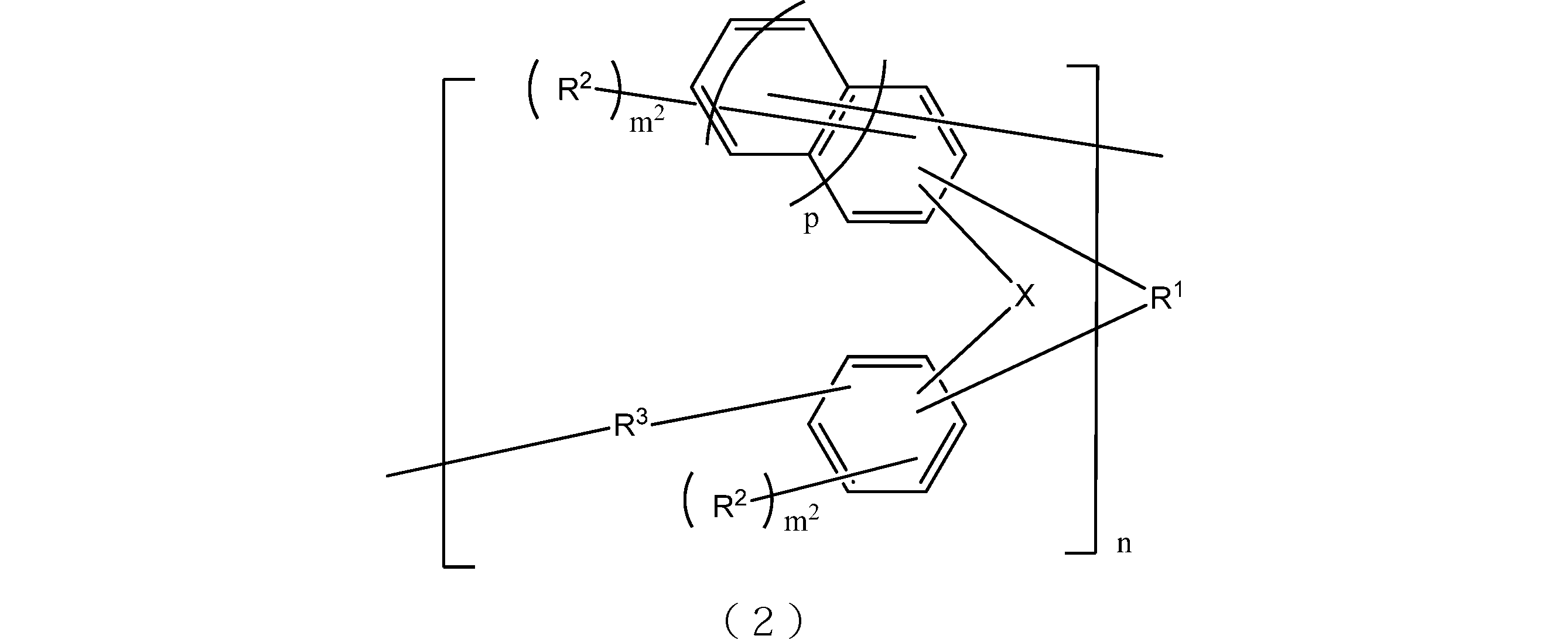
(式(2)中、Xは、各々独立して、酸素原子又は硫黄原子であり、R1は、単結合又は炭素数1~30の2n価の炭化水素基であり、該炭化水素基は、環式炭化水素基、二重結合、ヘテロ原子又は炭素数6~30の芳香族基を有していてもよく、R2は、各々独立して、炭素数1~10の直鎖状、分岐状若しくは環状のアルキル基、炭素数6~10のアリール基、炭素数2~10のアルケニル基又は水酸基であり、ここで、R2の少なくとも1つは水酸基であり、R3は、各々独立して、単結合又は炭素数1~20の直鎖状若しくは分岐状のアルキレン基であり、m2は、各々独立して、1~3の整数であり、nは、1~4の整数であり、pは、0又は1である。) A lower layer film-forming material for lithography containing a resin having a structure represented by the following general formula (2).
(In the formula (2), each X is independently an oxygen atom or a sulfur atom, R 1 is a single bond or a 2n-valent hydrocarbon group having 1 to 30 carbon atoms, and the hydrocarbon group is , A cyclic hydrocarbon group, a double bond, a hetero atom, or an aromatic group having 6 to 30 carbon atoms, and each R 2 is independently a straight chain having 1 to 10 carbon atoms, A branched or cyclic alkyl group, an aryl group having 6 to 10 carbon atoms, an alkenyl group having 2 to 10 carbon atoms, or a hydroxyl group, wherein at least one of R 2 is a hydroxyl group, and each R 3 is independently A single bond or a linear or branched alkylene group having 1 to 20 carbon atoms, m 2 is each independently an integer of 1 to 3, and n is an integer of 1 to 4. Yes, p is 0 or 1.) - 有機溶媒をさらに含有する、請求項2~4のいずれか一項に記載のリソグラフィー用下層膜形成材料。 The material for forming a lower layer film for lithography according to any one of claims 2 to 4, further comprising an organic solvent.
- 酸発生剤をさらに含有する、請求項2~5のいずれか一項に記載のリソグラフィー用下層膜形成材料。 The material for forming an underlayer film for lithography according to any one of claims 2 to 5, further comprising an acid generator.
- 架橋剤をさらに含有する、請求項2~6のいずれか一項に記載のリソグラフィー用下層膜形成材料。 The material for forming a lower layer film for lithography according to any one of claims 2 to 6, further comprising a crosslinking agent.
- 請求項2~7のいずれか一項に記載のリソグラフィー用下層膜形成材料から形成される、リソグラフィー用下層膜。 A lithography lower layer film formed from the lithography lower layer film forming material according to any one of claims 2 to 7.
- 基板上に、請求項2~7のいずれか一項に記載の下層膜形成材料を用いて下層膜を形成する工程(A-1)と、
前記下層膜上に、少なくとも1層のフォトレジスト層を形成する工程(A-2)と、
前記工程(A-2)の後、前記フォトレジスト層の所定の領域に放射線を照射し、アルカリ現像を行う工程(A-3)と、
を有する、パターン形成方法。 A step (A-1) of forming a lower layer film on the substrate using the lower layer film forming material according to any one of claims 2 to 7;
Forming at least one photoresist layer on the lower layer film (A-2);
After the step (A-2), a step (A-3) of irradiating a predetermined region of the photoresist layer with radiation to perform alkali development;
A pattern forming method. - 基板上に、請求項2~7のいずれか一項に記載の下層膜形成材料を用いて下層膜を形成する工程(B-1)と、
前記下層膜上に、珪素原子を含有するレジスト中間層膜材料を用いて中間層膜を形成する工程(B-2)と、
前記中間層膜上に、少なくとも1層のフォトレジスト層を形成する工程(B-3)と、
前記工程(B-3)の後、前記フォトレジスト層の所定の領域に放射線を照射し、アルカリ現像してレジストパターンを形成する工程(B-4)と、
前記工程(B-4)の後、前記レジストパターンをマスクとして前記中間層膜をエッチングし、得られた中間層膜パターンをエッチングマスクとして前記下層膜をエッチングし、得られた下層膜パターンをエッチングマスクとして基板をエッチングすることで基板にパターンを形成する工程(B-5)と、
を有する、パターン形成方法。
A step (B-1) of forming a lower layer film on the substrate using the lower layer film forming material according to any one of claims 2 to 7;
Forming an intermediate layer film on the lower layer film using a resist intermediate layer film material containing silicon atoms (B-2);
Forming at least one photoresist layer on the intermediate film (B-3);
After the step (B-3), a step (B-4) of forming a resist pattern by irradiating a predetermined region of the photoresist layer with radiation and performing alkali development;
After the step (B-4), the intermediate layer film is etched using the resist pattern as a mask, the lower layer film is etched using the obtained intermediate layer film pattern as an etching mask, and the obtained lower layer film pattern is etched. Forming a pattern on the substrate by etching the substrate as a mask (B-5);
A pattern forming method.
Priority Applications (5)
| Application Number | Priority Date | Filing Date | Title |
|---|---|---|---|
| CN201480007952.4A CN104981463B (en) | 2013-02-08 | 2014-02-04 | Compound, lower layer film for lithography form material, lower layer film for lithography and pattern formation method |
| US14/766,697 US9828355B2 (en) | 2013-02-08 | 2014-02-04 | Compound, material for forming underlayer film for lithography, underlayer film for lithography and pattern forming method |
| JP2014560762A JP6390911B2 (en) | 2013-02-08 | 2014-02-04 | COMPOUND, LITHOGRAPHIC LOWER FILM FORMING MATERIAL, LITHOGRAPHY LOWER FILM AND PATTERN FORMING METHOD |
| EP14749377.9A EP2955175B1 (en) | 2013-02-08 | 2014-02-04 | Use of 9-[1,1'-biphenyl]-4-yl-9h-xanthene-2,7-diol and similar compounds for forming resins for use in underlayer films for lithography and in pattern forming methods |
| KR1020157021508A KR102154109B1 (en) | 2013-02-08 | 2014-02-04 | Compound, material for forming underlayer film for lithography, underlayer film for lithography, and pattern formation method |
Applications Claiming Priority (2)
| Application Number | Priority Date | Filing Date | Title |
|---|---|---|---|
| JP2013023529 | 2013-02-08 | ||
| JP2013-023529 | 2013-02-08 |
Publications (2)
| Publication Number | Publication Date |
|---|---|
| WO2014123102A1 true WO2014123102A1 (en) | 2014-08-14 |
| WO2014123102A9 WO2014123102A9 (en) | 2015-04-30 |
Family
ID=51299696
Family Applications (1)
| Application Number | Title | Priority Date | Filing Date |
|---|---|---|---|
| PCT/JP2014/052524 WO2014123102A1 (en) | 2013-02-08 | 2014-02-04 | Compound, material for forming underlayer film for lithography, underlayer film for lithography, and pattern formation method |
Country Status (7)
| Country | Link |
|---|---|
| US (1) | US9828355B2 (en) |
| EP (1) | EP2955175B1 (en) |
| JP (1) | JP6390911B2 (en) |
| KR (1) | KR102154109B1 (en) |
| CN (1) | CN104981463B (en) |
| TW (1) | TWI632139B (en) |
| WO (1) | WO2014123102A1 (en) |
Cited By (5)
| Publication number | Priority date | Publication date | Assignee | Title |
|---|---|---|---|---|
| WO2016163456A1 (en) * | 2015-04-07 | 2016-10-13 | 三菱瓦斯化学株式会社 | Material for forming underlayer film for lithography, composition for forming underlayer film for lithography, underlayer film for lithography, and pattern formation method |
| WO2017014191A1 (en) * | 2015-07-22 | 2017-01-26 | 三菱瓦斯化学株式会社 | Compound, resin, underlayer film forming material for lithography, composition for forming underlayer film for lithography, underlayer film for lithography, resist pattern forming method, circuit pattern forming method, and purification method |
| WO2018101463A1 (en) * | 2016-12-02 | 2018-06-07 | 三菱瓦斯化学株式会社 | Compound, resin, composition, pattern formation method, and purification method |
| WO2018159707A1 (en) * | 2017-02-28 | 2018-09-07 | 三菱瓦斯化学株式会社 | Method for purifying compound or resin, and method for producing composition |
| JPWO2017111165A1 (en) * | 2015-12-25 | 2018-10-18 | 三菱瓦斯化学株式会社 | Compound, resin, composition, resist pattern forming method, and circuit pattern forming method |
Families Citing this family (9)
| Publication number | Priority date | Publication date | Assignee | Title |
|---|---|---|---|---|
| WO2014123102A1 (en) | 2013-02-08 | 2014-08-14 | 三菱瓦斯化学株式会社 | Compound, material for forming underlayer film for lithography, underlayer film for lithography, and pattern formation method |
| US10377734B2 (en) | 2013-02-08 | 2019-08-13 | Mitsubishi Gas Chemical Company, Inc. | Resist composition, method for forming resist pattern, polyphenol derivative for use in the composition |
| JP6388126B2 (en) * | 2013-02-08 | 2018-09-12 | 三菱瓦斯化学株式会社 | COMPOUND, LITHOGRAPHIC LOWER FILM FORMING MATERIAL, LITHOGRAPHY LOWER FILM AND PATTERN FORMING METHOD |
| KR20170099908A (en) | 2014-12-25 | 2017-09-01 | 미쯔비시 가스 케미칼 컴파니, 인코포레이티드 | Compound, resin, underlayer film forming material for lithography, underlayer film for lithography, pattern forming method and purification method |
| WO2016158168A1 (en) | 2015-03-31 | 2016-10-06 | 三菱瓦斯化学株式会社 | Compound, resist composition, and method for forming resist pattern in which same is used |
| US11480877B2 (en) | 2015-03-31 | 2022-10-25 | Mitsubishi Gas Chemical Company, Inc. | Resist composition, method for forming resist pattern, and polyphenol compound used therein |
| WO2017038645A1 (en) | 2015-08-31 | 2017-03-09 | 三菱瓦斯化学株式会社 | Material for forming underlayer films for lithography, composition for forming underlayer films for lithography, underlayer film for lithography and method for producing same, pattern forming method, resin, and purification method |
| WO2017038643A1 (en) | 2015-08-31 | 2017-03-09 | 三菱瓦斯化学株式会社 | Material for forming underlayer films for lithography, composition for forming underlayer films for lithography, underlayer film for lithography and method for producing same, and resist pattern forming method |
| KR20180050665A (en) | 2015-09-10 | 2018-05-15 | 미쯔비시 가스 케미칼 컴파니, 인코포레이티드 | COMPOSITION, RESIN, RESIST COMPOSITION OR RADIATION RADIATIVE COMPOSITION, RESIST PATTERN FORMING METHOD, AMORPHOUS FILM PRODUCTION METHOD, LITHOGRAPHY ROW LAYER FILM FORMING MATERIAL, COMPOSITION FOR FORMING LITHOGRAPHY UNDERLAY FILM |
Citations (18)
| Publication number | Priority date | Publication date | Assignee | Title |
|---|---|---|---|---|
| JPH07215833A (en) * | 1994-01-28 | 1995-08-15 | Noevir Co Ltd | Skin external preparation |
| JPH1025220A (en) * | 1996-07-10 | 1998-01-27 | Noevir Co Ltd | Preparation for external use for skin |
| JP2002214769A (en) * | 2001-01-18 | 2002-07-31 | Fuji Photo Film Co Ltd | Radiation sensitive positive type resist composition |
| JP2002334869A (en) | 2001-02-07 | 2002-11-22 | Tokyo Electron Ltd | Method and device for forming silicon nitride film, and method for preprocessing of cleaning thereof |
| JP2004177668A (en) | 2002-11-27 | 2004-06-24 | Tokyo Ohka Kogyo Co Ltd | Base layer film forming material for multilayer resist process, and wiring formation method using the same |
| WO2004066377A1 (en) | 2003-01-24 | 2004-08-05 | Tokyo Electron Limited | Method of cvd for forming silicon nitride film on substrate |
| JP2004271838A (en) | 2003-03-07 | 2004-09-30 | Shin Etsu Chem Co Ltd | Resist underlayer film material and pattern forming method |
| JP2005250434A (en) | 2004-02-04 | 2005-09-15 | Shin Etsu Chem Co Ltd | Resist underlayer film material and pattern forming method |
| JP2007226204A (en) | 2006-01-25 | 2007-09-06 | Shin Etsu Chem Co Ltd | Antireflection film material, substrate and patterning process |
| JP2007226170A (en) | 2006-01-27 | 2007-09-06 | Shin Etsu Chem Co Ltd | Antireflection film material, substrate having antireflection film and pattern forming method |
| JP2009108313A (en) * | 2007-10-10 | 2009-05-21 | Sumitomo Chemical Co Ltd | Polymeric compound and polymeric luminous element using it |
| WO2009072465A1 (en) | 2007-12-07 | 2009-06-11 | Mitsubishi Gas Chemical Company, Inc. | Composition for forming base film for lithography and method for forming multilayer resist pattern |
| WO2011034062A1 (en) | 2009-09-15 | 2011-03-24 | 三菱瓦斯化学株式会社 | Aromatic hydrocarbon resin and composition for forming underlayer film for lithography |
| JP2011150023A (en) * | 2010-01-19 | 2011-08-04 | Shin-Etsu Chemical Co Ltd | Composition for forming resist underlayer film, method for forming resist underlayer film, and patterning method |
| JP2012001687A (en) * | 2010-06-21 | 2012-01-05 | Shin-Etsu Chemical Co Ltd | Naphthalene derivative, resist underlayer film material, resist underlayer film forming method, and pattern forming method |
| JP2012145897A (en) * | 2011-01-14 | 2012-08-02 | Shin Etsu Chem Co Ltd | Resist underlayer film material and pattern forming method using the same |
| WO2013024779A1 (en) * | 2011-08-12 | 2013-02-21 | 三菱瓦斯化学株式会社 | Underlayer film-forming material for lithography, underlayer film for lithography, and pattern formation method |
| WO2013066067A1 (en) * | 2011-11-02 | 2013-05-10 | 주식회사 동진쎄미켐 | Phenol monomer, polymer for forming a resist underlayer film including same, and composition for a resist underlayer film including same |
Family Cites Families (57)
| Publication number | Priority date | Publication date | Assignee | Title |
|---|---|---|---|---|
| US2100798A (en) | 1933-05-02 | 1937-11-30 | Ig Farbenindustrie Ag | Condensation products of carbenium compounds and process of preparing the same |
| US2007107A (en) | 1934-03-07 | 1935-07-02 | Bottrill David Hugh | Combined soap and massage articles |
| US2546872A (en) * | 1947-10-10 | 1951-03-27 | Ciba Ltd | Hydroxy-compounds of the benzoxanthene series and process of making same |
| US3947468A (en) | 1971-05-26 | 1976-03-30 | General Electric Company | Production of dibenzopyrans, their isomeric fluorenols and dibenzothiopyrans |
| US4579758A (en) | 1981-01-16 | 1986-04-01 | The B. F. Goodrich Company | Internally coated reaction vessel for use in olefinic polymerization |
| JPH01283280A (en) | 1988-05-06 | 1989-11-14 | Asahi Denka Kogyo Kk | Novel epoxy compound and production thereof |
| JP2919142B2 (en) | 1990-12-27 | 1999-07-12 | 株式会社東芝 | Photosensitive composition and pattern forming method using the same |
| JPH0649402A (en) | 1992-08-04 | 1994-02-22 | Nippon Kayaku Co Ltd | Solder resist ink composition and its cured product |
| JPH06242607A (en) | 1993-02-18 | 1994-09-02 | Mitsubishi Electric Corp | Positive type resist composition and pattern forming method using the same |
| JP3112053B2 (en) * | 1994-01-28 | 2000-11-27 | 日本電気硝子株式会社 | Cover glass for solid-state imaging device |
| JPH1172925A (en) | 1997-07-03 | 1999-03-16 | Toshiba Corp | Undercoat layer composition and pattern forming method using the same |
| EP1311396A4 (en) | 2000-08-14 | 2005-06-08 | Silverbrook Res Pty Ltd | Interface surface printer using invisible ink |
| US6844273B2 (en) | 2001-02-07 | 2005-01-18 | Tokyo Electron Limited | Precleaning method of precleaning a silicon nitride film forming system |
| JP2002334896A (en) | 2001-05-07 | 2002-11-22 | Nagase & Co Ltd | Method for forming bump electrode |
| JP2002341542A (en) | 2001-05-18 | 2002-11-27 | Hitachi Chem Co Ltd | Positive photosensitive resin composition, method for manufacturing pattern and electronic parts |
| US6784228B2 (en) * | 2001-07-12 | 2004-08-31 | Dainippon Ink And Chemicals, Inc. | Epoxy resin composition, cured article thereof, novel epoxy resin, novel phenol compound, and process for preparing the same |
| JP3985165B2 (en) | 2001-08-20 | 2007-10-03 | 日産化学工業株式会社 | Antireflection film forming composition for lithography |
| EP1300403A1 (en) | 2001-10-02 | 2003-04-09 | Aventis Pharma S.A. | Process for the manufacture of hypoxyxylerone derivatives |
| TWI258635B (en) | 2002-11-27 | 2006-07-21 | Tokyo Ohka Kogyo Co Ltd | Undercoating material for wiring, embedded material, and wiring formation method |
| US20040186776A1 (en) | 2003-01-28 | 2004-09-23 | Llach Eduardo F. | System for automatically selling and purchasing highly targeted and dynamic advertising impressions using a mixture of price metrics |
| KR20060071423A (en) * | 2003-09-18 | 2006-06-26 | 미츠비시 가스 가가쿠 가부시키가이샤 | Compound for resist and radiation-sensitive composition |
| JP4614056B2 (en) | 2003-09-18 | 2011-01-19 | 三菱瓦斯化学株式会社 | Resist compound and radiation-sensitive composition |
| US7871751B2 (en) * | 2004-04-15 | 2011-01-18 | Mitsubishi Gas Chemical Company, Inc. | Resist composition |
| KR101168249B1 (en) | 2004-05-14 | 2012-07-30 | 닛산 가가쿠 고교 가부시키 가이샤 | Antireflective film-forming composition containing vinyl ether compound |
| JP4966484B2 (en) | 2004-07-22 | 2012-07-04 | 大阪瓦斯株式会社 | Fluorene compound and method for producing the same |
| JP4678195B2 (en) | 2005-02-03 | 2011-04-27 | 三菱瓦斯化学株式会社 | Phenanthrenequinone derivative and method for producing the same |
| JP2007019294A (en) | 2005-07-08 | 2007-01-25 | Konica Minolta Holdings Inc | Organic semiconductor material, organic semiconductor film, organic semiconductor element, and organic thin film transistor |
| JP4659678B2 (en) | 2005-12-27 | 2011-03-30 | 信越化学工業株式会社 | Photoresist underlayer film forming material and pattern forming method |
| KR101011599B1 (en) | 2006-01-25 | 2011-01-27 | 히다치 가세고교 가부시끼가이샤 | Phenol resin and resin compositions |
| JP2009098155A (en) | 2006-02-08 | 2009-05-07 | Mitsubishi Gas Chem Co Inc | Radiation-sensitive composition |
| TW200741353A (en) * | 2006-02-27 | 2007-11-01 | Mitsubishi Gas Chemical Co | Compound for forming antireflective film and antireflective film |
| JP2007262398A (en) | 2006-03-01 | 2007-10-11 | Hitachi Chem Co Ltd | Epoxy resin composition and electronic part device |
| JP2007326847A (en) | 2006-03-31 | 2007-12-20 | Honshu Chem Ind Co Ltd | New polynuclear polyphenol compound |
| KR101430529B1 (en) | 2006-08-28 | 2014-08-18 | 도소 가부시키가이샤 | Heteroacene derivative, tetrahaloterphenyl derivative, and their production methods |
| JP4910168B2 (en) | 2006-09-07 | 2012-04-04 | Jsr株式会社 | Resist underlayer film forming composition and pattern forming method |
| JP4858136B2 (en) | 2006-12-06 | 2012-01-18 | 三菱瓦斯化学株式会社 | Radiation-sensitive resist composition |
| JP5092492B2 (en) | 2007-03-28 | 2012-12-05 | Dic株式会社 | Thermosetting polyimide resin composition |
| JP5446118B2 (en) | 2007-04-23 | 2014-03-19 | 三菱瓦斯化学株式会社 | Radiation sensitive composition |
| JP2009073738A (en) | 2007-09-18 | 2009-04-09 | Idemitsu Kosan Co Ltd | Polycarboxylate compound, photoresist substrate and photoresist composition |
| JP5249578B2 (en) | 2007-12-26 | 2013-07-31 | 大阪瓦斯株式会社 | Epoxy compound having fluorene skeleton |
| WO2009119201A1 (en) | 2008-03-28 | 2009-10-01 | Jsr株式会社 | Resist underlayer film, composition for resist underlayer film formation, and method for resist underlayer film formation |
| CN102046726B (en) | 2008-05-27 | 2013-12-25 | 松下电器产业株式会社 | Epoxy resin composition for printed wiring board, solder resist composition, resin film, resin sheet, prepreg, metal foil with resin, cover lay, and flexible printed wiring board |
| JP5118073B2 (en) | 2009-01-26 | 2013-01-16 | 信越化学工業株式会社 | Resist underlayer film forming method and pattern forming method using the same |
| JP2010219295A (en) | 2009-03-17 | 2010-09-30 | Mitsui Chemicals Inc | Organic transistor |
| JP5513825B2 (en) | 2009-09-28 | 2014-06-04 | 大阪ガスケミカル株式会社 | Method for producing alcohol having fluorene skeleton |
| JP5466927B2 (en) | 2009-11-19 | 2014-04-09 | 大阪瓦斯株式会社 | Fluorene polyester oligomer and method for producing the same |
| WO2011148603A1 (en) | 2010-05-26 | 2011-12-01 | 三菱瓦斯化学株式会社 | Cyclic compound purification method |
| JP5556773B2 (en) | 2010-09-10 | 2014-07-23 | 信越化学工業株式会社 | Naphthalene derivative and method for producing the same, resist underlayer film material, resist underlayer film forming method and pattern forming method |
| US8742403B2 (en) | 2011-03-08 | 2014-06-03 | Samsung Electronics Co., Ltd. | Xanthene based semiconductor compositions |
| WO2012165507A1 (en) | 2011-06-03 | 2012-12-06 | 三菱瓦斯化学株式会社 | Phenolic resin and material for forming underlayer film for lithography |
| EP2743769B1 (en) | 2011-08-12 | 2017-03-22 | Mitsubishi Gas Chemical Company, Inc. | Resist composition, resist pattern formation method, polyphenol compound used therein, and alcohol compound capable of being derived therefrom |
| JP5698184B2 (en) | 2011-09-02 | 2015-04-08 | 信越化学工業株式会社 | Positive resist material and pattern forming method |
| JP5958734B2 (en) | 2011-10-17 | 2016-08-02 | 三菱瓦斯化学株式会社 | Novel epoxy compound and method for producing the same |
| US10377734B2 (en) * | 2013-02-08 | 2019-08-13 | Mitsubishi Gas Chemical Company, Inc. | Resist composition, method for forming resist pattern, polyphenol derivative for use in the composition |
| WO2014123102A1 (en) | 2013-02-08 | 2014-08-14 | 三菱瓦斯化学株式会社 | Compound, material for forming underlayer film for lithography, underlayer film for lithography, and pattern formation method |
| WO2014123005A1 (en) | 2013-02-08 | 2014-08-14 | 三菱瓦斯化学株式会社 | Novel aryl compound and method for producing same |
| JP6388126B2 (en) * | 2013-02-08 | 2018-09-12 | 三菱瓦斯化学株式会社 | COMPOUND, LITHOGRAPHIC LOWER FILM FORMING MATERIAL, LITHOGRAPHY LOWER FILM AND PATTERN FORMING METHOD |
-
2014
- 2014-02-04 WO PCT/JP2014/052524 patent/WO2014123102A1/en active Application Filing
- 2014-02-04 CN CN201480007952.4A patent/CN104981463B/en active Active
- 2014-02-04 EP EP14749377.9A patent/EP2955175B1/en active Active
- 2014-02-04 US US14/766,697 patent/US9828355B2/en active Active
- 2014-02-04 JP JP2014560762A patent/JP6390911B2/en active Active
- 2014-02-04 KR KR1020157021508A patent/KR102154109B1/en active IP Right Grant
- 2014-02-07 TW TW103104080A patent/TWI632139B/en active
Patent Citations (18)
| Publication number | Priority date | Publication date | Assignee | Title |
|---|---|---|---|---|
| JPH07215833A (en) * | 1994-01-28 | 1995-08-15 | Noevir Co Ltd | Skin external preparation |
| JPH1025220A (en) * | 1996-07-10 | 1998-01-27 | Noevir Co Ltd | Preparation for external use for skin |
| JP2002214769A (en) * | 2001-01-18 | 2002-07-31 | Fuji Photo Film Co Ltd | Radiation sensitive positive type resist composition |
| JP2002334869A (en) | 2001-02-07 | 2002-11-22 | Tokyo Electron Ltd | Method and device for forming silicon nitride film, and method for preprocessing of cleaning thereof |
| JP2004177668A (en) | 2002-11-27 | 2004-06-24 | Tokyo Ohka Kogyo Co Ltd | Base layer film forming material for multilayer resist process, and wiring formation method using the same |
| WO2004066377A1 (en) | 2003-01-24 | 2004-08-05 | Tokyo Electron Limited | Method of cvd for forming silicon nitride film on substrate |
| JP2004271838A (en) | 2003-03-07 | 2004-09-30 | Shin Etsu Chem Co Ltd | Resist underlayer film material and pattern forming method |
| JP2005250434A (en) | 2004-02-04 | 2005-09-15 | Shin Etsu Chem Co Ltd | Resist underlayer film material and pattern forming method |
| JP2007226204A (en) | 2006-01-25 | 2007-09-06 | Shin Etsu Chem Co Ltd | Antireflection film material, substrate and patterning process |
| JP2007226170A (en) | 2006-01-27 | 2007-09-06 | Shin Etsu Chem Co Ltd | Antireflection film material, substrate having antireflection film and pattern forming method |
| JP2009108313A (en) * | 2007-10-10 | 2009-05-21 | Sumitomo Chemical Co Ltd | Polymeric compound and polymeric luminous element using it |
| WO2009072465A1 (en) | 2007-12-07 | 2009-06-11 | Mitsubishi Gas Chemical Company, Inc. | Composition for forming base film for lithography and method for forming multilayer resist pattern |
| WO2011034062A1 (en) | 2009-09-15 | 2011-03-24 | 三菱瓦斯化学株式会社 | Aromatic hydrocarbon resin and composition for forming underlayer film for lithography |
| JP2011150023A (en) * | 2010-01-19 | 2011-08-04 | Shin-Etsu Chemical Co Ltd | Composition for forming resist underlayer film, method for forming resist underlayer film, and patterning method |
| JP2012001687A (en) * | 2010-06-21 | 2012-01-05 | Shin-Etsu Chemical Co Ltd | Naphthalene derivative, resist underlayer film material, resist underlayer film forming method, and pattern forming method |
| JP2012145897A (en) * | 2011-01-14 | 2012-08-02 | Shin Etsu Chem Co Ltd | Resist underlayer film material and pattern forming method using the same |
| WO2013024779A1 (en) * | 2011-08-12 | 2013-02-21 | 三菱瓦斯化学株式会社 | Underlayer film-forming material for lithography, underlayer film for lithography, and pattern formation method |
| WO2013066067A1 (en) * | 2011-11-02 | 2013-05-10 | 주식회사 동진쎄미켐 | Phenol monomer, polymer for forming a resist underlayer film including same, and composition for a resist underlayer film including same |
Non-Patent Citations (2)
| Title |
|---|
| NISHIYAMA, TOMIHIRO ET AL.: "Antioxidant activities of fused heterocyclic compounds, xanthene-2,7-diols with BHT or catechol skeleton", POLYMER DEGRADATION AND STABILITY, vol. 62, no. 3, 1998, pages 529 - 534, XP004294575 * |
| PROTIVA, MIROSLAV ET AL.: "Potential metabolites of tricyclic neuroleptics: 2,8- dihydroxy and 3,8-dihydroxy derivatives of 10- (4-methylpiperazino)-10,11-dihydrodibenzo[b,f] thiepin", NEUROTROPIC AND PSYCHOTROPIC AGENTS., vol. 44, no. 10, 1979, pages 2987 - 2996, XP055276881 * |
Cited By (14)
| Publication number | Priority date | Publication date | Assignee | Title |
|---|---|---|---|---|
| WO2016163456A1 (en) * | 2015-04-07 | 2016-10-13 | 三菱瓦斯化学株式会社 | Material for forming underlayer film for lithography, composition for forming underlayer film for lithography, underlayer film for lithography, and pattern formation method |
| WO2017014191A1 (en) * | 2015-07-22 | 2017-01-26 | 三菱瓦斯化学株式会社 | Compound, resin, underlayer film forming material for lithography, composition for forming underlayer film for lithography, underlayer film for lithography, resist pattern forming method, circuit pattern forming method, and purification method |
| CN107848983A (en) * | 2015-07-22 | 2018-03-27 | 三菱瓦斯化学株式会社 | Compound, resin, lower layer film for lithography form material, lower layer film for lithography is formed with composition, lower layer film for lithography and corrosion-resisting pattern forming method, circuit pattern forming method and purification process |
| JPWO2017014191A1 (en) * | 2015-07-22 | 2018-05-24 | 三菱瓦斯化学株式会社 | Compound, resin, lower film forming material for lithography, composition for forming lower film for lithography, lower film for lithography and resist pattern forming method, circuit pattern forming method, and purification method |
| CN107848983B (en) * | 2015-07-22 | 2021-07-09 | 三菱瓦斯化学株式会社 | Compound, resin, material for forming underlayer film for lithography, resist pattern, method for forming circuit pattern, and method for purifying resist pattern |
| US10364314B2 (en) | 2015-07-22 | 2019-07-30 | Mitsubishi Gas Chemical Company, Inc. | Compound, resin, material for forming underlayer film for lithography, composition for forming underlayer film for lithography, underlayer film for lithography, resist pattern forming method, circuit pattern forming method, and purification method |
| JPWO2017111165A1 (en) * | 2015-12-25 | 2018-10-18 | 三菱瓦斯化学株式会社 | Compound, resin, composition, resist pattern forming method, and circuit pattern forming method |
| US11130724B2 (en) * | 2015-12-25 | 2021-09-28 | Mitsubishi Gas Chemical Company, Inc. | Compound, resin, composition, resist pattern formation method, and circuit pattern formation method |
| JPWO2018101463A1 (en) * | 2016-12-02 | 2019-10-24 | 三菱瓦斯化学株式会社 | Compound, resin, composition, pattern formation method and purification method |
| WO2018101463A1 (en) * | 2016-12-02 | 2018-06-07 | 三菱瓦斯化学株式会社 | Compound, resin, composition, pattern formation method, and purification method |
| JP7090843B2 (en) | 2016-12-02 | 2022-06-27 | 三菱瓦斯化学株式会社 | Compounds, resins, compositions, pattern forming methods and purification methods |
| WO2018159707A1 (en) * | 2017-02-28 | 2018-09-07 | 三菱瓦斯化学株式会社 | Method for purifying compound or resin, and method for producing composition |
| JPWO2018159707A1 (en) * | 2017-02-28 | 2020-01-09 | 三菱瓦斯化学株式会社 | Method for purifying compound or resin, and method for producing composition |
| JP2022184850A (en) * | 2017-02-28 | 2022-12-13 | 三菱瓦斯化学株式会社 | Purification method of compound or resin, and production method of composition |
Also Published As
| Publication number | Publication date |
|---|---|
| US20150376158A1 (en) | 2015-12-31 |
| CN104981463B (en) | 2018-04-13 |
| EP2955175B1 (en) | 2018-04-04 |
| EP2955175A1 (en) | 2015-12-16 |
| EP2955175A4 (en) | 2016-08-31 |
| KR20150113008A (en) | 2015-10-07 |
| WO2014123102A9 (en) | 2015-04-30 |
| US9828355B2 (en) | 2017-11-28 |
| TW201500351A (en) | 2015-01-01 |
| CN104981463A (en) | 2015-10-14 |
| TWI632139B (en) | 2018-08-11 |
| KR102154109B1 (en) | 2020-09-09 |
| JP6390911B2 (en) | 2018-09-19 |
| JPWO2014123102A1 (en) | 2017-02-02 |
Similar Documents
| Publication | Publication Date | Title |
|---|---|---|
| JP6573217B2 (en) | Compound, resin, lower layer film forming material for lithography, lower layer film for lithography, pattern forming method, and method for purifying compound or resin | |
| JP5979384B2 (en) | Lower layer film forming material for lithography, lower layer film for lithography and pattern forming method | |
| JP6064904B2 (en) | Phenol-based resin and lower film forming material for lithography | |
| JP6094947B2 (en) | Resin having fluorene structure and material for forming lower layer film for lithography | |
| JP6390911B2 (en) | COMPOUND, LITHOGRAPHIC LOWER FILM FORMING MATERIAL, LITHOGRAPHY LOWER FILM AND PATTERN FORMING METHOD | |
| US10364314B2 (en) | Compound, resin, material for forming underlayer film for lithography, composition for forming underlayer film for lithography, underlayer film for lithography, resist pattern forming method, circuit pattern forming method, and purification method | |
| WO2011034062A1 (en) | Aromatic hydrocarbon resin and composition for forming underlayer film for lithography | |
| WO2016104214A1 (en) | Compound, resin, underlayer film forming material for lithography, underlayer film for lithography, pattern forming method and purification method | |
| JP6388126B2 (en) | COMPOUND, LITHOGRAPHIC LOWER FILM FORMING MATERIAL, LITHOGRAPHY LOWER FILM AND PATTERN FORMING METHOD | |
| WO2016129679A1 (en) | Compound, resin, lithography underlayer film forming material, lithography underlayer film forming composition, lithography underlayer film, method for forming resist pattern, method for forming circuit pattern, and method for purifying compound or resin | |
| WO2017038643A1 (en) | Material for forming underlayer films for lithography, composition for forming underlayer films for lithography, underlayer film for lithography and method for producing same, and resist pattern forming method | |
| WO2012090408A1 (en) | Aromatic hydrocarbon resin, composition for forming lithographic underlayer film, and method for forming multilayer resist pattern | |
| WO2016158457A1 (en) | Compound, resin, and method for purifying same, underlayer film formation material for lithography, underlayer film forming composition, and underlayer film, and method for forming resist pattern and method for forming circuit pattern | |
| WO2016143635A1 (en) | Compound, resin, material for forming underlayer film for lithography, underlayer film for lithography, pattern forming method, and method for purifying compound or resin |
Legal Events
| Date | Code | Title | Description |
|---|---|---|---|
| 121 | Ep: the epo has been informed by wipo that ep was designated in this application |
Ref document number: 14749377 Country of ref document: EP Kind code of ref document: A1 |
|
| ENP | Entry into the national phase |
Ref document number: 2014560762 Country of ref document: JP Kind code of ref document: A |
|
| WWE | Wipo information: entry into national phase |
Ref document number: 2014749377 Country of ref document: EP |
|
| ENP | Entry into the national phase |
Ref document number: 20157021508 Country of ref document: KR Kind code of ref document: A |
|
| WWE | Wipo information: entry into national phase |
Ref document number: 14766697 Country of ref document: US |
|
| NENP | Non-entry into the national phase |
Ref country code: DE |