WO2014119345A1 - 巨大磁気抵抗効果素子およびそれを用いた電流センサ - Google Patents
巨大磁気抵抗効果素子およびそれを用いた電流センサ Download PDFInfo
- Publication number
- WO2014119345A1 WO2014119345A1 PCT/JP2014/050150 JP2014050150W WO2014119345A1 WO 2014119345 A1 WO2014119345 A1 WO 2014119345A1 JP 2014050150 W JP2014050150 W JP 2014050150W WO 2014119345 A1 WO2014119345 A1 WO 2014119345A1
- Authority
- WO
- WIPO (PCT)
- Prior art keywords
- magnetic layer
- alloy
- gmr element
- layer
- free magnetic
- Prior art date
Links
Images


Classifications
-
- G—PHYSICS
- G01—MEASURING; TESTING
- G01R—MEASURING ELECTRIC VARIABLES; MEASURING MAGNETIC VARIABLES
- G01R33/00—Arrangements or instruments for measuring magnetic variables
- G01R33/02—Measuring direction or magnitude of magnetic fields or magnetic flux
- G01R33/06—Measuring direction or magnitude of magnetic fields or magnetic flux using galvano-magnetic devices
- G01R33/09—Magnetoresistive devices
- G01R33/093—Magnetoresistive devices using multilayer structures, e.g. giant magnetoresistance sensors
-
- G—PHYSICS
- G01—MEASURING; TESTING
- G01R—MEASURING ELECTRIC VARIABLES; MEASURING MAGNETIC VARIABLES
- G01R15/00—Details of measuring arrangements of the types provided for in groups G01R17/00 - G01R29/00, G01R33/00 - G01R33/26 or G01R35/00
- G01R15/14—Adaptations providing voltage or current isolation, e.g. for high-voltage or high-current networks
- G01R15/20—Adaptations providing voltage or current isolation, e.g. for high-voltage or high-current networks using galvano-magnetic devices, e.g. Hall-effect devices, i.e. measuring a magnetic field via the interaction between a current and a magnetic field, e.g. magneto resistive or Hall effect devices
- G01R15/205—Adaptations providing voltage or current isolation, e.g. for high-voltage or high-current networks using galvano-magnetic devices, e.g. Hall-effect devices, i.e. measuring a magnetic field via the interaction between a current and a magnetic field, e.g. magneto resistive or Hall effect devices using magneto-resistance devices, e.g. field plates
-
- G—PHYSICS
- G11—INFORMATION STORAGE
- G11B—INFORMATION STORAGE BASED ON RELATIVE MOVEMENT BETWEEN RECORD CARRIER AND TRANSDUCER
- G11B5/00—Recording by magnetisation or demagnetisation of a record carrier; Reproducing by magnetic means; Record carriers therefor
- G11B5/127—Structure or manufacture of heads, e.g. inductive
- G11B5/33—Structure or manufacture of flux-sensitive heads, i.e. for reproduction only; Combination of such heads with means for recording or erasing only
- G11B5/39—Structure or manufacture of flux-sensitive heads, i.e. for reproduction only; Combination of such heads with means for recording or erasing only using magneto-resistive devices or effects
- G11B5/3903—Structure or manufacture of flux-sensitive heads, i.e. for reproduction only; Combination of such heads with means for recording or erasing only using magneto-resistive devices or effects using magnetic thin film layers or their effects, the films being part of integrated structures
-
- H—ELECTRICITY
- H10—SEMICONDUCTOR DEVICES; ELECTRIC SOLID-STATE DEVICES NOT OTHERWISE PROVIDED FOR
- H10N—ELECTRIC SOLID-STATE DEVICES NOT OTHERWISE PROVIDED FOR
- H10N50/00—Galvanomagnetic devices
- H10N50/10—Magnetoresistive devices
-
- H—ELECTRICITY
- H10—SEMICONDUCTOR DEVICES; ELECTRIC SOLID-STATE DEVICES NOT OTHERWISE PROVIDED FOR
- H10N—ELECTRIC SOLID-STATE DEVICES NOT OTHERWISE PROVIDED FOR
- H10N50/00—Galvanomagnetic devices
- H10N50/80—Constructional details
- H10N50/85—Magnetic active materials
-
- G—PHYSICS
- G11—INFORMATION STORAGE
- G11B—INFORMATION STORAGE BASED ON RELATIVE MOVEMENT BETWEEN RECORD CARRIER AND TRANSDUCER
- G11B5/00—Recording by magnetisation or demagnetisation of a record carrier; Reproducing by magnetic means; Record carriers therefor
- G11B5/127—Structure or manufacture of heads, e.g. inductive
- G11B5/33—Structure or manufacture of flux-sensitive heads, i.e. for reproduction only; Combination of such heads with means for recording or erasing only
- G11B5/39—Structure or manufacture of flux-sensitive heads, i.e. for reproduction only; Combination of such heads with means for recording or erasing only using magneto-resistive devices or effects
- G11B2005/3996—Structure or manufacture of flux-sensitive heads, i.e. for reproduction only; Combination of such heads with means for recording or erasing only using magneto-resistive devices or effects large or giant magnetoresistive effects [GMR], e.g. as generated in spin-valve [SV] devices
Definitions
- the present invention relates to a giant magnetoresistive element (hereinafter referred to as a GMR (Giant Magneto Resistance) element) and a current sensor using the GMR element.
- GMR Giant Magneto Resistance
- magnetic sensors that detect a magnetic field are widely used in magnetic application products that are widely used.
- a current sensor that measures a current in a noncontact manner by detecting a magnetic field generated by a current flowing in a conductor is also widely used.
- current sensors include applications that contactlessly measure relatively small currents, such as household appliances, and applications that contactlessly measure relatively large currents, such as electric vehicles and hybrid cars.
- FIG. 8 is an explanatory view of a current sensor disclosed in Patent Document 1.
- the current sensor 110 disclosed in Patent Document 1 is configured by embedding a magnetoresistive effect element 101 such as a GMR element formed on a semiconductor chip 116 in a housing 117.
- the current sensor 110 is disposed at a predetermined position on the conductor 111 through which the current flows, and measures the current by detecting a magnetic field generated by the current.
- FIG. 9 is an explanatory view of the GMR element disclosed in Patent Document 2.
- the GMR device 201 disclosed in Patent Document 2 includes an antiferromagnetic layer (PtMn) 205, a pinned magnetic layer (CoFe / Ru / CoFe) 206, a spacer layer (CuO) 207, and a free magnetic layer. It has a stacked structure of (CoFe / NiFe) 208 and a protective layer (Ta) 209 in this order.
- the free magnetic layer 208 has a stacked structure of CoFe having a large spin polarization ratio and NiFe having an excellent soft magnetic characteristic, so that the rate of change in resistance ⁇ R / R min is large.
- a GMR element with a small hysteresis of the magnetization curve is realized.
- magnetic applied products include a magnetic head of a hard disk drive and a tunnel magnetoresistive element (hereinafter, a TMR element) often used as a magnetoresistive memory (MRAM).
- TMR element tunnel magnetoresistive element
- MRAM magnetoresistive memory
- FIG. 10 is an explanatory view of a TMR element disclosed in Patent Document 3.
- the TMR element 301 disclosed in Patent Document 3 includes, as shown in FIG. 10, an antiferromagnetic layer (IrMn) 305, a first pinned magnetic layer (CoFe) 306a, a nonmagnetic intermediate layer (antiferromagnetic coupling layer) It has a structure in which Ru) 306b, a second pinned magnetic layer (CoFeB) 306c, a tunnel barrier layer (MgO) 307, a free magnetic layer 308, and a protective layer 309 are stacked in this order.
- IrMn antiferromagnetic layer
- CoFe first pinned magnetic layer
- MgO tunnel barrier layer
- free magnetic layer 308 a free magnetic layer
- the TMR element 301 is known to obtain a large resistance change ratio ⁇ R / R min (MR ratio) by crystal orientation of MgO of the tunnel barrier layer 307 in the (001) direction. It is also known that MgO is crystallographically oriented in the rock salt type (001) direction by film formation on an amorphous underlayer. Therefore, in Patent Document 3, the tunnel barrier layer (MgO) 307 is formed on the second pinned magnetic layer (CoFeB) 306c formed as an amorphous film.
- CoFeB of the second pinned magnetic layer 306c formed as an amorphous film is thereafter crystallized according to the crystal structure of the MgO interface of the tunnel barrier layer 307 by heat treatment.
- the reason is that CoFeB of the second pinned magnetic layer 306 c has a body-centered cubic structure on the side in contact with the tunnel barrier layer (MgO) 307 and is crystallographically oriented in the (001) direction, resulting in a large resistance change ratio. This is because ⁇ R / R min is realized.
- this is a structure unique to a TMR element having a tunnel barrier layer and can not be applied to a GMR element.
- JP 2007-121283 A Japanese Patent Application Publication No. 2004-164837 JP, 2010-097981, A
- the output linear range which is the range having the linearity of
- the first method is to shorten the dimension in the width direction orthogonal to the longitudinal direction of the long pattern of the GMR element to increase the shape magnetic anisotropy.
- the dimension in the width direction of the long pattern is almost shortened to the limit due to the demand for miniaturization and low cost.
- the second method is to increase the magnetic moment Ms ⁇ t of the free magnetic layer.
- the rate of change in resistance ⁇ R / R min is significantly reduced.
- the object of the present invention is to solve such problems, and to provide a giant magnetoresistance effect element having a large output linear range as well as a large resistance change ratio ⁇ R / R min and a current sensor using the same. It is to be.
- a pinned magnetic layer whose magnetization is pinned, a free magnetic layer whose magnetization is changed by an external magnetic field, and a spacer layer located between the pinned magnetic layer and the free magnetic layer And the free magnetic layer is formed by laminating a CoFe alloy and a CoFeB alloy.
- the rate of change in resistance ⁇ R / R min of the GMR element can be increased.
- the film thickness of the CoFe alloy is preferably 2 nm or more and 4 nm or less. With such an embodiment, the rate of change in resistance ⁇ R / R min can be further increased. As a result, the output linear range of the GMR element can be further increased.
- the film thickness of the CoFeB alloy is preferably 5 nm or more and 14 nm or less. With such an embodiment, the magnetostriction can be suppressed to ⁇ 1 ppm or less. Therefore, the hysteresis generated due to the stress is suppressed, so that a GMR device with high accuracy can be realized.
- the CoFeB alloy preferably has an amorphous structure.
- the resistivity of the CoFeB alloy can be increased, so the rate of change in resistance ⁇ R / R min of the GMR element can be further increased.
- CoFe alloy Co X Fe 100-X alloy, and the CoFeB alloy (Co Y Fe 100-Y) 100-Z B Z alloy
- X is 80 atomic% ⁇ X ⁇ 100 atomic%
- Y is 80
- Z is 10 atomic% ⁇ Z ⁇ 30 atomic%.
- the current sensor of the present invention is characterized by using the giant magnetoresistance effect element according to any one of claims 1 to 5.
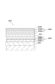
- FIG. 1 is an explanatory view showing a layer configuration of a giant magnetoresistive element according to an embodiment of the present invention.
- FIG. 2 is an explanatory view of a current sensor according to an embodiment of the present invention.
- the current sensor 10 of the present embodiment is a magnetic proportional current sensor. As shown in FIG. 2, the current sensor 10 of the present embodiment includes a bridge circuit including two GMR elements 1 a and 1 b as magnetic detection elements and two fixed resistance elements 2 a and 2 b. The current sensor 10 is disposed in the vicinity of the conductor 11 through which the measured current I flows, and detects an induced magnetic field H generated by the measured current I. At this time, the current sensor 10 obtains an output substantially proportional to the induced magnetic field H generated by the current I to be measured.
- one terminal of each of the GMR element 1b and the fixed resistance element 2a is connected to the power supply terminal V dd, and one terminal of each of the GMR element 1a and the fixed resistance element 2b is connected to the ground terminal GND It is done.
- GMR elements 1a other terminal of the fixed resistance element 2a is connected, it has a first output Out 1
- second output Out are respectively GMR element 1b and the other terminal of the fixed resistance element 2b connected 2 It has become.
- the GMR elements 1a and 1b have the characteristic that the electrical resistance changes when the induction magnetic field H generated by the current to be measured I is applied, so the first output according to the induction magnetic field H generated by the current to be measured I Out 1 and the second output Out 2 change. Voltage difference between the first output Out 1 and the second output Out 2 is substantially proportional to the induced magnetic field H, the voltage difference is the output of the current sensor 10.
- the configuration of the bridge circuit is not limited to that shown in FIG.
- a bridge circuit may be configured by combining one GMR element and three fixed resistance elements, or a bridge circuit may be configured by combining four GMR elements.
- the GMR element 1 includes the lower gap layer 3, the seed layer 4, the antiferromagnetic layer 5, the pinned magnetic layer 6, the spacer layer 7, the free magnetic layer 8, and the protective layer 9 as shown in FIG. It has the structure laminated in order.
- the lower gap layer 3 is formed on a silicon substrate (not shown) or the like, and made of an insulating material such as alumina (Al 2 O 3 ).
- the seed layer 4 is an underlayer for arranging crystal growth of each layer laminated on the antiferromagnetic layer 5 and the antiferromagnetic layer 5 and is formed of a NiFe alloy, a NiCr alloy, a NiFeCr alloy, Cr or the like.
- the antiferromagnetic layer 5 generates a large exchange coupling magnetic field with the pinned magnetic layer 6 by heat treatment, thereby fixing the magnetization direction of the pinned magnetic layer 6 (fixed magnetization direction).
- the antiferromagnetic layer 5 is formed of a PtMn alloy or an X-Mn alloy (wherein X is any one or more elements of Pd, Ir, Rh, Ru, Os, Ni, and Fe). Ru.
- Pt-Mn-Y (wherein Y is any one or more elements of Pd, Ir, Rh, Ru, Au, Ag, Os, Cr, Ni, Ar, Ne, Xe, and Kr). ) Formed of alloy.
- These alloys have a disordered face-centered cubic structure (fcc) immediately after film formation, but when heat-treated, they form a CuAuI (CuAu1) type ordered face-centered tetragonal structure (fct). To metamorphose. Therefore, when the antiferromagnetic layer 5 is formed using the above-described alloy, a large exchange coupling magnetic field can be generated between the antiferromagnetic layer 5 and the pinned magnetic layer 6 by heat treatment.
- the pinned magnetic layer 6 has a laminated ferri-pinned structure consisting of a first pinned magnetic layer 6a, a nonmagnetic intermediate layer 6b, and a second pinned magnetic layer 6c.
- the magnetization of the first pinned magnetic layer 6a is the same as that of the antiferromagnetic layer 5 Is fixed in the width direction of the long pattern by exchange coupling, and the magnetization of the second pinned magnetic layer 6c is 180 ° different (antiparallel) from the magnetization direction of the first pinned magnetic layer 6a via the nonmagnetic intermediate layer 6b. It is fixed.
- the pinned magnetic layer 6 has a laminated ferri-pinned structure, the antiparallel coupling between the first and second pinned magnetic layers 6a and 6c, the first pinned magnetic layer 6a, and the By the synergetic effect of exchange coupling between the ferromagnetic layers 5, the magnetization direction of the pinned magnetic layer 6 can be fixed more stably.
- the pinned magnetic layer 6 may have a single-layer structure.
- the first and second pinned magnetic layers 6a and 6c are formed of a ferromagnetic material, and are formed of, for example, a NiFe alloy, Co, a CoNiFe alloy, a CoFe alloy or a CoNi alloy. In particular, it is preferable to be formed of a CoFe alloy or Co.
- the first pinned magnetic layer 6a and the second pinned magnetic layer 6c are preferably formed of the same material.
- the nonmagnetic intermediate layer 6b is formed of a nonmagnetic material, and is formed of one or more of Ru, Rh, Pd, Ir, Os, Re, Cr, Cu, Pt, and Au. Can. In particular, it is preferable to be formed of Ru or Cu.
- the spacer layer 7 is a layer that prevents the magnetic coupling between the pinned magnetic layer 6 and the free magnetic layer 8 and is a layer through which a detection current mainly flows.
- the spacer layer 7 is formed of a conductive nonmagnetic material such as Cu, Cr, Au or Ag. In particular, it is preferable to be formed of Cu.
- the free magnetic layer 8 is configured by laminating a first free magnetic layer 8a and a second free magnetic layer 8b.
- the first free magnetic layer 8a is a CoFe alloy
- the second free magnetic layer 8b is a CoFeB alloy having an amorphous structure.
- Y is 80 at% ⁇ Y ⁇ 100 at%
- Z is 10 at% ⁇ Z ⁇ 30 at%.
- the protective layer 9 is formed of Ta (tantalum) or the like.
- the electrical resistance R of the GMR element changes according to the magnetization direction of the free magnetic layer.
- the electric resistance R of the GMR element becomes the minimum electric resistance R min when the magnetization direction of the free magnetic layer is parallel to the fixed magnetization direction of the fixed magnetic layer. That is because, as shown in FIG. 1, in addition to the spacer layer 7, the free magnetic layer 8, ie, the first free magnetic layer 8a and the second free magnetic layer 8b, also contribute to the flow of electrons.
- the electrical resistance R of the GMR element increases as the magnetization direction of the free magnetic layer is directed in a direction other than parallel to the fixed magnetization direction of the pinned magnetic layer.
- the electrical resistance R of the GMR element becomes maximum electrical resistance R max when the magnetization direction of the free magnetic layer is directed in a direction antiparallel to the fixed magnetization direction of the fixed magnetic layer.
- the change in resistance difference RR min is usually expressed as ⁇ R, and the resistance change rate ⁇ R / R min is defined.
- the electrons are free magnetic layer 8, ie, the first free magnetic layer 8a and the second free magnetic layer. It is shunted to 8b (shunt loss). Therefore, in order to further increase the maximum electrical resistance R max and increase the rate of change in resistance ⁇ R / R min , it is necessary to reduce the shunting electrons (shunt loss). Therefore, it is preferable that the electric resistance of the second free magnetic layer 8 b (CoFeB alloy) is large in order to reduce the shunting electrons (shunt loss).
- FIG. 3 is experimental data showing the relationship between the rate of change in resistance ⁇ R / R min and Ms ⁇ t.
- the prior art GMR element 201 free magnetic layer is disclosed in Patent Document 2 is a Co 90 Fe 10 / NiFe multilayer film case (shown in FIG. 9) (hereinafter, referred to as comparative example), resistance
- the relationship between the rate of change ⁇ R / R min and the free magnetic layer Ms ⁇ t is compared.
- (Co 90 Fe 10) 80 B 20 means that the Co 90 Fe 10 alloy B (boron) was added 20 atomic%.
- Ms ⁇ t is the magnetic moment per unit area (magnetic film thickness) of the magnetic layer, and is the product (Ms ⁇ t) of the saturation magnetization Ms of the magnetic layer and the film thickness t of the magnetic layer.
- Ms ⁇ t illustrated on the horizontal axis of FIG. 3 is the product of the saturation magnetization Ms of each free magnetic layer and the thickness t of the free magnetic layer.
- Ms ⁇ t illustrated in FIG. 3 is compared by changing the film thickness of the (Co 90 Fe 10 ) 80 B 20 alloy in the GMR element 1 of the embodiment under each saturation magnetization Ms being constant.
- the film thickness is changed by changing the film thickness of the NiFe alloy.
- the vertical axis in FIG. 3 is the rate of change in resistance ⁇ R / R min .
- the GMR element 1 of the embodiment has a larger rate of change in resistance ⁇ R / R min than the GMR element 201 of the comparative example. Therefore, compared to the GMR element 201 of the comparative example, the GMR element 1 of the embodiment has a large resistance change ratio ⁇ R / R min and is high in sensitivity to the fluctuation of the external magnetic field. Therefore, the current sensor 10 (shown in FIG. 2) using the GMR element 1 according to the present embodiment is a current to be measured I (shown in FIG. 2) as compared to the current sensor using the GMR element 201 of the prior art. Highly sensitive to fluctuations.
- the GMR element 1 of the example has a smaller decrease in ⁇ R / R min due to the increase of M S ⁇ t. Therefore, even if the output linear range is increased, it is possible to realize the GMR element 1 having a large resistance change rate ⁇ R / R min .
- the GMR element 1 of the example has a smaller change in resistance change rate ⁇ R / R min due to the thickness variation of the free magnetic layer. Therefore, the GMR element 1 according to the present embodiment and the current sensor 10 (shown in FIG.
- the GMR element 1 including the free magnetic layer Co 90 Fe 10 / NiFe of the prior art, and the GMR element As compared with the current sensor using 201, the rate of change in resistance ⁇ R / R min is stable and highly accurate.
- the reason why the GMR element 1 of the embodiment has a larger ⁇ R / R min than the GMR element 201 of the comparative example and a small decrease in ⁇ R / R min with an increase in M S ⁇ t is the resistivity of the NiFe alloy Since the resistivity (approximately 100 ⁇ cm) of the CoFeB alloy is as large as approximately 5 times that of (approximately 20 ⁇ cm), electrons shunted to the CoFeB alloy, ie, shunt loss can be suppressed compared to electrons shunted to the NiFe alloy. It is.
- FIG. 4 is experimental data showing the relationship between the rate of change in resistance ⁇ R / R min and the film thickness of the free magnetic layer, in the case where the free magnetic layer is a Co 90 Fe 10 / (Co 90 Fe 10 ) 80 B 20 laminated film. is there.
- the vertical axis in FIG. 4 is the rate of change in resistance ⁇ R / R min
- the horizontal axis is the film thickness of the first free magnetic layer 8 a (Co 90 Fe 10 alloy).
- the relationship between the rate of change in resistance ⁇ R / R min and the thickness of the first free magnetic layer 8 a is illustrated using the thickness of the second free magnetic layer 8 b ((Co 90 Fe 10 ) 80 B 20 ) as a parameter. .
- the film thickness of the first free magnetic layer 8a (CoFe alloy) (shown in FIG. 1) is in the range of 2 nm to 4 nm as shown in FIG. 4, and the film of the second free magnetic layer 8b (shown in FIG. 1) It can be seen that the rate of change in resistance ⁇ R / R min of the GMR element 1 (shown in FIG. 1) is large regardless of the thickness. Therefore, if the film thickness of the first free magnetic layer 8a (shown in FIG. 1) is in the range of 2 nm to 4 nm, the GMR element 1 (shown in FIG. 1) according to the present embodiment Sensitivity is high. Therefore, in the current sensor 10 (shown in FIG. 2) using the GMR element 1 (shown in FIG.
- the thickness of the first free magnetic layer 8a (shown in FIG. 1) is in the range of 2 nm to 4 nm.
- the sensitivity to the fluctuation of the measured current I (shown in FIG. 2) is high. Therefore, the film thickness of the first free magnetic layer 8a (CoFe alloy) (shown in FIG. 1) is preferably 2 nm or more and 4 nm or less.
- FIG. 5 is experimental data showing the relationship between the magnetostriction ⁇ of the free magnetic layer and the film thickness of the free magnetic layer, and is a case where the free magnetic layer is a Co 90 Fe 10 / (Co 90 Fe 10 ) 80 B 20 laminated film. .
- the vertical axis of FIG. 5 is the magnetostriction ⁇ of the free magnetic layer, and the horizontal axis is the thickness of the first free magnetic layer 8 a (Co 90 Fe 10 ).
- the relationship between the magnetostriction ⁇ of the free magnetic layer and the thickness of the first free magnetic layer 8a is illustrated with the thickness of the second free magnetic layer 8b ((Co 90 Fe 10 ) 80 B 20 ) as a parameter.
- the magnetostriction ⁇ of the free magnetic layer is preferably close to zero.
- the thickness of the second free magnetic layer 8 b is 5 nm to 14 nm.
- the magnetostriction ⁇ of the free magnetic layer is ⁇ 1 ppm or less, which is preferable.
- the film thickness of the second free magnetic layer 8b is 5 nm or more and 14 nm or less, the hysteresis generated due to the stress of the GMR element 1 (shown in FIG. 1) according to the present embodiment is suppressed. Therefore, if the film thickness of the second free magnetic layer 8b is 5 nm or more and 14 nm or less, a highly accurate GMR element is possible, and a current sensor using the highly accurate GMR element can be realized.
- FIG. 6 is experimental data showing the relationship between output linear range and sensitivity in a current sensor.
- the vertical axis in FIG. 6 is the output linear range where the linearity of the output of the current sensor can be obtained, and the maximum deviation (mV) between the output curve and its linear approximation straight line is the difference between the maximum value and the minimum value of the output curve. It is a range ( ⁇ mT) of the induction magnetic field H (shown in FIG. 2) whose percentage divided by (full scale) is 0.3% or less.
- the horizontal axis in FIG. 6 is the slope of the output (mV) with respect to the induced magnetic field H (mT), that is, the sensitivity (mV / mT).
- the current sensor using the conventional GMR element in which the free magnetic layer is Co 90 Fe 10 / Ni 81 Fe 19 and the free magnetic layer is Co 90 Fe 10 / (Co 90 Fe 10 ) 80 B 20 The current sensor 10 (shown in FIG. 2) using the GMR element of the present embodiment is compared and evaluated. Then, 6, the thickness of the Co 90 Fe 10 and (Co 90 Fe 10) 80 B 20 of the present embodiment, a 2.5nm and 6.0 nm, instead of 2.5nm and 7.5 nm, also The film thicknesses of the prior art Co 90 Fe 10 and Ni 81 Fe 19 are illustrated by changing them to 1.0 nm and 7.0 nm, and 1.0 nm and 9.0 nm.
- the output linear range is wider when compared with the current sensor of the prior art with the same sensitivity. Further, as shown in FIG. 6, the current sensor 10 (shown in FIG. 2) of the present embodiment has higher sensitivity when compared in the same output linear range as the current sensor of the prior art.
- the output linear range of the GMR element can be broadened by increasing the magnetic moment Ms ⁇ t of the free magnetic layer. Therefore, the output linear range of the current sensor using the GMR element having a large magnetic moment Ms ⁇ t is wide.
- the rate of change in resistance ⁇ R / R min of the GMR element decreases.
- the GMR element 1 shown in FIG. 3
- the free magnetic layer of the GMR element is a Co 90 Fe 10 alloy / (Co 90 Fe 10) 80 B 20 alloy, as shown in FIGS. 3 to 6, it can be seen the characteristics of the GMR element is good. Therefore, the free magnetic layer, when representing a Co X Fe 100-X alloy / (Co Y Fe 100-Y ) 100-Z B Z alloy, X and Y is preferably near 90 atomic%, Z is 20 atomic% The vicinity of is preferable. In particular, X and Y are preferably 80 atomic percent or more and less than 100 atomic percent. Moreover, it is preferable that Z is 10 atomic% or more and 30 atomic% or less.
- the second free magnetic layer 8b When Z is less than 10 atomic%, the second free magnetic layer 8b, i.e. (Co Y Fe 100-Y) become 100-Z B Z alloy changes the crystal structure from an amorphous structure, a second free magnetic layer The electrical resistance of 8 b decreases, and the rate of change in resistance ⁇ R / R min decreases. Also, when Z is greater than 30 atomic%, the second free magnetic layer 8b, i.e. (Co Y Fe 100-Y) 100-Z saturation magnetization Ms of B Z alloy is reduced, and increasing the thickness t Also makes it difficult to increase the magnetic moment Ms ⁇ t. Therefore, it is preferable that Z be 10 atomic percent or more and 30 atomic percent or less.
- the ferromagnetic properties of the second free magnetic layer 8 b that is, (Co Y Fe 100 -Y ) 100 -Z BZ alloy is maintained, and the free magnetic layer 8b, i.e. the (Co Y Fe 100-Y) 100-Z B Z alloy can be an amorphous structure, it is possible to increase the resistance change rate [Delta] R / R min of the GMR element. Therefore, a current sensor using a GMR element having a large resistance change rate ⁇ R / R min can be realized.
- the second free magnetic layer 8 b is a CoFeB alloy, but the present invention is not limited to this. It is also possible to add B to a ferromagnetic material such as NiFe to form an amorphous structure, or to add an impurity such as P other than B to a ferromagnetic material such as NiFe to form an amorphous structure.
- the GMR element of this embodiment is used for a current sensor, it is not limited to this.
- it can be used for a magnetic sensor that obtains a linear output, such as a magnetic sensor that detects the position of a linearly moving magnetic body (magnet).
- a method of manufacturing the current sensor 10 illustrated in FIG. 2 will be described.
- An aluminum oxide film or the like which is an insulating layer is formed on a substrate such as a silicon substrate by a method such as sputtering.
- the laminated films constituting the GMR elements 1a and 1b shown in FIG. 2, as shown in FIG. 1, that is, the antiferromagnetic layer 5, the fixed magnetic layer 6, the spacer layer 7, the free magnetic layer 8 and the like are sputtered etc.
- the GMR elements 1a and 1b are formed by photolithography and etching. Then, heat treatment (for example, holding at 270 ° C.
- films constituting the fixed resistance elements 2a and 2b illustrated in FIG. 2 are also formed by a method such as sputtering, and the fixed resistance elements 2a and 2b are formed by photolithography and etching.
- the electrode material is formed into a film by a method such as sputtering, and an electrode or the like for electrically connecting the GMR elements 1a and 1b and the fixed resistance elements 2a and 2b is formed by photolithography and etching.
- the fixed resistance elements 2a and 2b are elements whose electric resistance does not change due to an external magnetic field. Therefore, although it can also be formed of an electrode material such as Cu or Al, in the GMR element 1 shown in FIG. 1, the spacer layer 7 and the free magnetic layer 8 can be configured in the reverse order. In the latter case, since the magnetization direction of the free magnetic layer 8 is fixed by the fixed magnetic layer 6, the electric resistance does not change due to the external magnetic field. In addition, since the GMR elements 1a and 1b and the fixed resistance elements 2a and 2b are made of the same electrode material, the electric resistance changes in the same manner as the temperature changes, and the temperature characteristics are excellent.
- FIG. 7 is an explanatory view of a current sensor according to a modification.
- the current sensor 10 of the present embodiment is a magnetic proportional current sensor as shown in FIG. 2, the present invention is not limited to this, and a magnetic balanced current sensor is also possible.
- the magnetic balance type current sensor 20 is disposed in the vicinity of the conductor 11 through which the measured current I flows.
- the magnetic balance type current sensor 20 includes a feedback circuit 15 that generates a magnetic field (canceling magnetic field) that cancels an induced magnetic field H caused by the current I to be measured flowing through the conductor 11.
- the feedback circuit 15 includes a feedback coil 12 wound in a direction to cancel a magnetic field generated by the current I to be measured, two GMR elements 1a and 2b as magnetic detection elements, and two fixed resistance elements 2a and 2b. Have.
- the electrical resistance of the two GMR elements 1a and 1b changes due to the application of the induction magnetic field H from the current to be measured I.
- the two GMR elements 1a and 1b constitute a bridge circuit together with the two fixed resistance elements 2a and 2b. By using the bridge circuit in this manner, a highly sensitive magnetic balanced current sensor 20 can be realized.
- the power supply terminal V dd is connected to the connection point between the GMR element 1b and the fixed resistance element 2a, and the ground is connected to the connection point between the GMR element 1a and the fixed resistance element 2b.
- the terminal GND is connected.
- one output is taken out from the connection point between GMR element 1a and fixed resistance element 2a, and another output is taken out from the connection point between GMR element 1b and fixed resistance element 2b. ing.
- These two outputs are amplified by the amplifier 13 and given to the feedback coil 12 as a current (feedback current). This feedback current corresponds to the voltage difference according to the induced magnetic field.
- a canceling magnetic field is generated in the feedback coil 12 to cancel the induced magnetic field.
- the measured current I is measured by the detection voltage V corresponding to the current flowing through the feedback coil 12 in an equilibrium state where the induction magnetic field and the cancellation magnetic field cancel each other.
Abstract
Description
図7は、変形例に係る電流センサの説明図である。本実施形態の電流センサ10は、図2に示すように、磁気比例式電流センサであるとしたが、これに限定されるものではなく、磁気平衡式電流センサも可能である。
2a、2b 固定抵抗素子
3 下部ギャップ層
4 シード層
5 反強磁性層
6 固定磁性層
6a 第1固定磁性層
6b 非磁性中間層
6c 第2固定磁性層
7 スペーサ層
8 フリー磁性層
8a 第1フリー磁性層
8b 第2フリー磁性層
9 保護層
10 電流センサ
11 導体 12 フィードバックコイル
13 増幅器
15 フィードバックコイル回路
Claims (6)
- 磁化が固定されている固定磁性層と、
磁化が外部磁界によって変化するフリー磁性層と、
前記固定磁性層と前記フリー磁性層との間に位置するスペーサ層と、
を有する巨大磁気抵抗効果素子であって、
前記フリー磁性層が、CoFe合金とCoFeB合金とが積層されてなることを特徴とする巨大磁気抵抗効果素子。 - 前記CoFe合金の膜厚が、2nm以上4nm以下であることを特徴とする請求項1に記載の巨大磁気抵抗効果素子。
- 前記CoFeB合金の膜厚が、5nm以上14nm以下であることを特徴とする請求項2に記載の巨大磁気抵抗効果素子。
- 前記CoFeB合金がアモルファス構造であることを特徴とする請求項1から請求項3のいずれか1項に記載の巨大磁気抵抗効果素子。
- 前記CoFe合金をCoXFe100-X合金、および前記CoFeB合金を(CoYFe100-Y)100-ZBZ合金とするとき、Xが80原子%≦X<100原子%、Yが80原子%≦Y<100原子%、およびZが10原子%≦Z≦30原子%であることを特徴とする請求項1から請求項4のいずれか1項に記載の巨大磁気抵抗効果素子。
- 請求項1から請求項5のいずれか1項に記載の巨大磁気抵抗効果素子を用いたことを特徴とする電流センサ。
Priority Applications (3)
| Application Number | Priority Date | Filing Date | Title |
|---|---|---|---|
| EP14746159.4A EP2953178B1 (en) | 2013-02-04 | 2014-01-08 | Giant magnetoresistive element and current sensor using same |
| JP2014559603A JP6039697B2 (ja) | 2013-02-04 | 2014-01-08 | 巨大磁気抵抗効果素子およびそれを用いた電流センサ |
| US14/789,781 US9523746B2 (en) | 2013-02-04 | 2015-07-01 | Giant magnetoresistance element and current sensor using the same |
Applications Claiming Priority (2)
| Application Number | Priority Date | Filing Date | Title |
|---|---|---|---|
| JP2013019805 | 2013-02-04 | ||
| JP2013-019805 | 2013-02-04 |
Related Child Applications (1)
| Application Number | Title | Priority Date | Filing Date |
|---|---|---|---|
| US14/789,781 Continuation US9523746B2 (en) | 2013-02-04 | 2015-07-01 | Giant magnetoresistance element and current sensor using the same |
Publications (1)
| Publication Number | Publication Date |
|---|---|
| WO2014119345A1 true WO2014119345A1 (ja) | 2014-08-07 |
Family
ID=51262059
Family Applications (1)
| Application Number | Title | Priority Date | Filing Date |
|---|---|---|---|
| PCT/JP2014/050150 WO2014119345A1 (ja) | 2013-02-04 | 2014-01-08 | 巨大磁気抵抗効果素子およびそれを用いた電流センサ |
Country Status (4)
| Country | Link |
|---|---|
| US (1) | US9523746B2 (ja) |
| EP (1) | EP2953178B1 (ja) |
| JP (1) | JP6039697B2 (ja) |
| WO (1) | WO2014119345A1 (ja) |
Cited By (2)
| Publication number | Priority date | Publication date | Assignee | Title |
|---|---|---|---|---|
| JP2015125012A (ja) * | 2013-12-25 | 2015-07-06 | 株式会社東芝 | 電流センサ及び電流センサモジュール |
| JP2017040509A (ja) * | 2015-08-18 | 2017-02-23 | アルプス電気株式会社 | 磁気センサおよび電流センサ |
Families Citing this family (1)
| Publication number | Priority date | Publication date | Assignee | Title |
|---|---|---|---|---|
| JP6724459B2 (ja) * | 2016-03-23 | 2020-07-15 | Tdk株式会社 | 磁気センサ |
Citations (6)
| Publication number | Priority date | Publication date | Assignee | Title |
|---|---|---|---|---|
| JPH10284768A (ja) * | 1997-04-10 | 1998-10-23 | Alps Electric Co Ltd | 磁気抵抗効果素子 |
| JP2001237472A (ja) * | 1999-06-17 | 2001-08-31 | Matsushita Electric Ind Co Ltd | 磁気抵抗効果素子および磁気抵抗効果記憶素子およびデジタル信号を記憶させる方法 |
| JP2004164837A (ja) | 2002-11-13 | 2004-06-10 | Hitachi Global Storage Technologies Netherlands Bv | ピン固定磁気層のプラズマ平滑化による強化gmr磁気ヘッド及びその製造方法 |
| JP2007121283A (ja) | 2005-10-08 | 2007-05-17 | Sentron Ag | 電流測定値用組立体群 |
| JP2009283963A (ja) * | 2001-10-12 | 2009-12-03 | Sony Corp | 磁気抵抗効果素子、磁気メモリ素子、磁気メモリ装置 |
| JP2010097981A (ja) | 2008-10-14 | 2010-04-30 | Fujitsu Ltd | トンネル磁気抵抗効果素子及び磁気記憶装置 |
Family Cites Families (13)
| Publication number | Priority date | Publication date | Assignee | Title |
|---|---|---|---|---|
| JPS59117915U (ja) | 1983-01-29 | 1984-08-09 | トヨタ自動車株式会社 | 自動車のステアリングセンサ |
| US7149105B2 (en) * | 2004-02-24 | 2006-12-12 | Infineon Technologies Ag | Magnetic tunnel junctions for MRAM devices |
| US7431961B2 (en) | 2004-12-10 | 2008-10-07 | Headway Technologies, Inc. | Composite free layer for CIP GMR device |
| US20080246104A1 (en) * | 2007-02-12 | 2008-10-09 | Yadav Technology | High Capacity Low Cost Multi-State Magnetic Memory |
| JP2008078378A (ja) | 2006-09-21 | 2008-04-03 | Alps Electric Co Ltd | トンネル型磁気検出素子及びその製造方法 |
| US9040178B2 (en) * | 2008-09-22 | 2015-05-26 | Headway Technologies, Inc. | TMR device with novel free layer structure |
| JP2010093117A (ja) * | 2008-10-09 | 2010-04-22 | Fujitsu Ltd | 磁気抵抗効果素子とその製造方法および情報記憶装置 |
| US8259420B2 (en) * | 2010-02-01 | 2012-09-04 | Headway Technologies, Inc. | TMR device with novel free layer structure |
| US8379350B2 (en) * | 2010-06-30 | 2013-02-19 | Tdk Corporation | CPP-type magnetoresistive element including spacer layer |
| US9028910B2 (en) * | 2010-12-10 | 2015-05-12 | Avalanche Technology, Inc. | MTJ manufacturing method utilizing in-situ annealing and etch back |
| JP2012069958A (ja) * | 2011-10-14 | 2012-04-05 | Toshiba Corp | 磁気記録素子 |
| US9252710B2 (en) * | 2012-11-27 | 2016-02-02 | Headway Technologies, Inc. | Free layer with out-of-plane anisotropy for magnetic device applications |
| US9082872B2 (en) * | 2013-01-02 | 2015-07-14 | Headway Technologies, Inc. | Magnetic read head with MR enhancements |
-
2014
- 2014-01-08 WO PCT/JP2014/050150 patent/WO2014119345A1/ja active Application Filing
- 2014-01-08 EP EP14746159.4A patent/EP2953178B1/en active Active
- 2014-01-08 JP JP2014559603A patent/JP6039697B2/ja active Active
-
2015
- 2015-07-01 US US14/789,781 patent/US9523746B2/en active Active
Patent Citations (6)
| Publication number | Priority date | Publication date | Assignee | Title |
|---|---|---|---|---|
| JPH10284768A (ja) * | 1997-04-10 | 1998-10-23 | Alps Electric Co Ltd | 磁気抵抗効果素子 |
| JP2001237472A (ja) * | 1999-06-17 | 2001-08-31 | Matsushita Electric Ind Co Ltd | 磁気抵抗効果素子および磁気抵抗効果記憶素子およびデジタル信号を記憶させる方法 |
| JP2009283963A (ja) * | 2001-10-12 | 2009-12-03 | Sony Corp | 磁気抵抗効果素子、磁気メモリ素子、磁気メモリ装置 |
| JP2004164837A (ja) | 2002-11-13 | 2004-06-10 | Hitachi Global Storage Technologies Netherlands Bv | ピン固定磁気層のプラズマ平滑化による強化gmr磁気ヘッド及びその製造方法 |
| JP2007121283A (ja) | 2005-10-08 | 2007-05-17 | Sentron Ag | 電流測定値用組立体群 |
| JP2010097981A (ja) | 2008-10-14 | 2010-04-30 | Fujitsu Ltd | トンネル磁気抵抗効果素子及び磁気記憶装置 |
Non-Patent Citations (1)
| Title |
|---|
| See also references of EP2953178A4 |
Cited By (3)
| Publication number | Priority date | Publication date | Assignee | Title |
|---|---|---|---|---|
| JP2015125012A (ja) * | 2013-12-25 | 2015-07-06 | 株式会社東芝 | 電流センサ及び電流センサモジュール |
| US9841444B2 (en) | 2013-12-25 | 2017-12-12 | Kabushiki Kaisha Toshiba | Current sensor and current sensor module |
| JP2017040509A (ja) * | 2015-08-18 | 2017-02-23 | アルプス電気株式会社 | 磁気センサおよび電流センサ |
Also Published As
| Publication number | Publication date |
|---|---|
| EP2953178B1 (en) | 2017-11-22 |
| US20150377985A1 (en) | 2015-12-31 |
| JP6039697B2 (ja) | 2016-12-07 |
| JPWO2014119345A1 (ja) | 2017-01-26 |
| US9523746B2 (en) | 2016-12-20 |
| EP2953178A1 (en) | 2015-12-09 |
| EP2953178A4 (en) | 2016-10-12 |
Similar Documents
| Publication | Publication Date | Title |
|---|---|---|
| US10254315B2 (en) | Current sensor, current measuring module, and smart meter | |
| US20180038899A1 (en) | Current sensor, current measuring module, and smart meter | |
| JP6199730B2 (ja) | 電流センサ及び電流センサモジュール | |
| JP2011064653A (ja) | 磁気センサおよびその製造方法 | |
| WO2013129276A1 (ja) | 磁気センサ素子 | |
| WO2012090631A1 (ja) | 磁気比例式電流センサ | |
| JP6686147B2 (ja) | 交換結合膜ならびにこれを用いた磁気抵抗効果素子および磁気検出装置 | |
| WO2018079404A1 (ja) | 磁気センサおよびその製造方法 | |
| JP5540299B2 (ja) | 電流センサ | |
| CN112578323A (zh) | 磁阻传感器及其制造方法 | |
| JP6951454B2 (ja) | 交換結合膜ならびにこれを用いた磁気抵抗効果素子および磁気検出装置 | |
| JP5447616B2 (ja) | 磁気センサの製造方法 | |
| US9523746B2 (en) | Giant magnetoresistance element and current sensor using the same | |
| JP5597305B2 (ja) | 電流センサ | |
| JP2011027633A (ja) | 磁気センサおよびその製造方法 | |
| KR102183263B1 (ko) | 자기 센서 및 전류 센서 | |
| JP5540326B2 (ja) | 電流センサ | |
| US11488758B2 (en) | Exchange coupling film, and magnetoresistive sensor and magnetic detector including the same | |
| JP2017040509A (ja) | 磁気センサおよび電流センサ | |
| JP6204391B2 (ja) | 磁気センサおよび電流センサ | |
| WO2010137606A1 (ja) | 磁気センサ | |
| JPWO2008102786A1 (ja) | 磁気検出装置 |
Legal Events
| Date | Code | Title | Description |
|---|---|---|---|
| 121 | Ep: the epo has been informed by wipo that ep was designated in this application |
Ref document number: 14746159 Country of ref document: EP Kind code of ref document: A1 |
|
| ENP | Entry into the national phase |
Ref document number: 2014559603 Country of ref document: JP Kind code of ref document: A |
|
| REEP | Request for entry into the european phase |
Ref document number: 2014746159 Country of ref document: EP |
|
| WWE | Wipo information: entry into national phase |
Ref document number: 2014746159 Country of ref document: EP |
|
| NENP | Non-entry into the national phase |
Ref country code: DE |