WO2014119045A1 - 半導体装置 - Google Patents
半導体装置 Download PDFInfo
- Publication number
- WO2014119045A1 WO2014119045A1 PCT/JP2013/076771 JP2013076771W WO2014119045A1 WO 2014119045 A1 WO2014119045 A1 WO 2014119045A1 JP 2013076771 W JP2013076771 W JP 2013076771W WO 2014119045 A1 WO2014119045 A1 WO 2014119045A1
- Authority
- WO
- WIPO (PCT)
- Prior art keywords
- protective film
- wiring layer
- semiconductor device
- semiconductor substrate
- electrode
- Prior art date
- Legal status (The legal status is an assumption and is not a legal conclusion. Google has not performed a legal analysis and makes no representation as to the accuracy of the status listed.)
- Ceased
Links
Images


Classifications
-
- H—ELECTRICITY
- H10—SEMICONDUCTOR DEVICES; ELECTRIC SOLID-STATE DEVICES NOT OTHERWISE PROVIDED FOR
- H10W—GENERIC PACKAGES, INTERCONNECTIONS, CONNECTORS OR OTHER CONSTRUCTIONAL DETAILS OF DEVICES COVERED BY CLASS H10
- H10W74/00—Encapsulations, e.g. protective coatings
- H10W74/10—Encapsulations, e.g. protective coatings characterised by their shape or disposition
- H10W74/131—Encapsulations, e.g. protective coatings characterised by their shape or disposition the semiconductor body being only partially enclosed
- H10W74/147—Encapsulations, e.g. protective coatings characterised by their shape or disposition the semiconductor body being only partially enclosed the encapsulations being multilayered
-
- H—ELECTRICITY
- H10—SEMICONDUCTOR DEVICES; ELECTRIC SOLID-STATE DEVICES NOT OTHERWISE PROVIDED FOR
- H10W—GENERIC PACKAGES, INTERCONNECTIONS, CONNECTORS OR OTHER CONSTRUCTIONAL DETAILS OF DEVICES COVERED BY CLASS H10
- H10W20/00—Interconnections in chips, wafers or substrates
- H10W20/40—Interconnections external to wafers or substrates, e.g. back-end-of-line [BEOL] metallisations or vias connecting to gate electrodes
- H10W20/49—Adaptable interconnections, e.g. fuses or antifuses
-
- H—ELECTRICITY
- H10—SEMICONDUCTOR DEVICES; ELECTRIC SOLID-STATE DEVICES NOT OTHERWISE PROVIDED FOR
- H10W—GENERIC PACKAGES, INTERCONNECTIONS, CONNECTORS OR OTHER CONSTRUCTIONAL DETAILS OF DEVICES COVERED BY CLASS H10
- H10W42/00—Arrangements for protection of devices
-
- H—ELECTRICITY
- H10—SEMICONDUCTOR DEVICES; ELECTRIC SOLID-STATE DEVICES NOT OTHERWISE PROVIDED FOR
- H10W—GENERIC PACKAGES, INTERCONNECTIONS, CONNECTORS OR OTHER CONSTRUCTIONAL DETAILS OF DEVICES COVERED BY CLASS H10
- H10W72/00—Interconnections or connectors in packages
- H10W72/50—Bond wires
- H10W72/59—Bond pads specially adapted therefor
-
- H—ELECTRICITY
- H10—SEMICONDUCTOR DEVICES; ELECTRIC SOLID-STATE DEVICES NOT OTHERWISE PROVIDED FOR
- H10W—GENERIC PACKAGES, INTERCONNECTIONS, CONNECTORS OR OTHER CONSTRUCTIONAL DETAILS OF DEVICES COVERED BY CLASS H10
- H10W72/00—Interconnections or connectors in packages
- H10W72/90—Bond pads, in general
- H10W72/921—Structures or relative sizes of bond pads
- H10W72/923—Bond pads having multiple stacked layers
-
- H—ELECTRICITY
- H10—SEMICONDUCTOR DEVICES; ELECTRIC SOLID-STATE DEVICES NOT OTHERWISE PROVIDED FOR
- H10W—GENERIC PACKAGES, INTERCONNECTIONS, CONNECTORS OR OTHER CONSTRUCTIONAL DETAILS OF DEVICES COVERED BY CLASS H10
- H10W72/00—Interconnections or connectors in packages
- H10W72/90—Bond pads, in general
- H10W72/941—Dispositions of bond pads
- H10W72/9415—Dispositions of bond pads relative to the surface, e.g. recessed, protruding
-
- H—ELECTRICITY
- H10—SEMICONDUCTOR DEVICES; ELECTRIC SOLID-STATE DEVICES NOT OTHERWISE PROVIDED FOR
- H10W—GENERIC PACKAGES, INTERCONNECTIONS, CONNECTORS OR OTHER CONSTRUCTIONAL DETAILS OF DEVICES COVERED BY CLASS H10
- H10W72/00—Interconnections or connectors in packages
- H10W72/90—Bond pads, in general
- H10W72/941—Dispositions of bond pads
- H10W72/942—Dispositions of bond pads relative to underlying supporting features, e.g. bond pads, RDLs or vias
-
- H—ELECTRICITY
- H10—SEMICONDUCTOR DEVICES; ELECTRIC SOLID-STATE DEVICES NOT OTHERWISE PROVIDED FOR
- H10W—GENERIC PACKAGES, INTERCONNECTIONS, CONNECTORS OR OTHER CONSTRUCTIONAL DETAILS OF DEVICES COVERED BY CLASS H10
- H10W72/00—Interconnections or connectors in packages
- H10W72/90—Bond pads, in general
- H10W72/951—Materials of bond pads
- H10W72/952—Materials of bond pads comprising metals or metalloids, e.g. PbSn, Ag or Cu
-
- H—ELECTRICITY
- H10—SEMICONDUCTOR DEVICES; ELECTRIC SOLID-STATE DEVICES NOT OTHERWISE PROVIDED FOR
- H10W—GENERIC PACKAGES, INTERCONNECTIONS, CONNECTORS OR OTHER CONSTRUCTIONAL DETAILS OF DEVICES COVERED BY CLASS H10
- H10W74/00—Encapsulations, e.g. protective coatings
Definitions
- the present invention relates to a semiconductor device including an electrode pad.
- Semiconductor devices are composed of a semiconductor substrate and a large number of circuit elements formed on the semiconductor substrate, and are built in various electronic devices.
- the semiconductor device is designed to have moisture resistance in order to protect circuit elements from moisture in the atmosphere.
- Patent Document 1 As a conventional semiconductor device considering moisture resistance, for example, there is a structure as shown in Patent Document 1.
- the semiconductor device described in Patent Document 1 includes a semiconductor substrate, a stacked body, a protective groove, a bonding pad, and a protective film.
- the stacked body is formed on a semiconductor substrate.
- One end of the laminate is scribed and exposed to the atmosphere.
- the protective groove is formed in the stacked body so that the surface of the semiconductor substrate is exposed.
- the bonding pad is formed on the laminate.
- the protective film covers the upper surface of the multilayer body and the side wall surface and the bottom surface of the protective groove except for the portion with the bonding pad.
- FIG. 5A is a plan view illustrating an example of a conventional semiconductor device.
- FIG. 5B is a cross-sectional view taken along the line A-A ′ of FIG.
- the surface facing the upper side in FIG. 5B is referred to as the upper surface
- the surface facing the lower side is referred to as the lower surface.
- FIG. 5A illustrates a part of the semiconductor device 1P.
- the semiconductor device 1P includes a semiconductor substrate 11, surface electrodes 21P, 22, 23P, first wiring layers 31P, 34, insulating layers 41P, 42P, second wiring layers 51P, 52P, 53, and protective films 61, 62, 63. And vias 71 and 74P.
- the surface electrodes 21P, 22 and 23P are in contact with the upper surface of the semiconductor substrate 11.
- the surface electrodes 21P, 22, and 23P are connected to each other and are electrically connected to each other.
- the first wiring layer 31P is formed on the upper surface of the surface electrode 23P through the via 74P.
- the first wiring layer 34 is formed on the upper surface of the surface electrode 22 via the protective film 61.
- the insulating layer 41P is formed on the upper surface of the semiconductor substrate 11 with the protective films 61 and 62 interposed therebetween.
- the insulating layer 42P is formed on the upper surface of the surface electrode 21P via the protective films 61 and 62, and is located between the first wiring layers 31P and 34.
- the insulating layers 41P and 42P are formed so as to be connected together with other insulating layers not shown.
- the insulating layers 41P and 42P are hygroscopic.
- the second wiring layer 51P is formed on the upper surface of the first wiring layer 31P via the via 71.
- the second wiring layer 52P is formed on the upper surface of the insulating layer 42P.
- the second wiring layer 53 is formed on the upper surface of the first wiring layer 34 via the protective film 62.
- the second wiring layers 51P, 52P, and 53 are connected to each other and are electrically connected to each other.
- the protective film 63 is formed on the surface of the semiconductor device 1P except for the upper surface of the second wiring layer 51P.
- the protective films 61, 62, and 63 have moisture resistance and adhesion between the protective films.
- the semiconductor device 1P is sealed with a mold resin or the like.
- the second wiring layer 51P is used as a bonding pad.
- the surface electrode 22, the first wiring layer 34, the second wiring layer 53, and the protective films 61 and 62 are used as MIMC (Metal-Insulator-Metal Capacitor).
- the bonding pads and the MIMC are connected by the surface electrodes 21P and 23P, the first wiring layer 31P, the second wiring layer 52P, and the vias 71 and 74P.
- the MIMC is connected to an external power source, an RF signal line, etc. by a bonding pad.
- Mold resin that seals semiconductor devices generally has hygroscopicity. For this reason, in the semiconductor device 1P shown in FIG. 5B, moisture in the atmosphere reaches the surface of the bonding pad through the path R1.
- the adhesion between the second wiring layer 51P and the protective film 63 is not sufficient to prevent moisture from entering. For this reason, moisture that has traveled along the path R1 enters the semiconductor device 1P through the path R2 between the second wiring layer 51P and the protective film 63.
- the insulating layers 41P and 42P are formed of a hygroscopic material. For this reason, the water
- Region A2 corresponds to the edge of the electrode of MIMC, and is where the electric field concentrates when a voltage is applied to MIMC.
- the protective film 62 in the region A2 reacts with moisture by applying a voltage to the MIMC. As a result, a short-circuit portion is generated in the protective film 62, so that the MIMC characteristics deteriorate.
- An object of the present invention is to improve the moisture resistance of a semiconductor device.
- the semiconductor device according to the present invention is configured as follows.
- the semiconductor device according to the present invention includes a semiconductor substrate, a wiring layer, a first protective film, an insulating layer, and a second protective film.
- the wiring layer is formed on the semiconductor substrate and used as an electrode pad.
- the first protective film is formed on the semiconductor substrate so as to surround the electrode pad when viewed from a direction perpendicular to the main surface of the semiconductor substrate, and has moisture resistance.
- the insulating layer is formed on the first protective film away from the electrode pad and has a hygroscopic property.
- the second protective film is continuously formed on the electrode pad, the insulating layer, and the first protective film, and opens at the center of the electrode pad.
- the second protective film has moisture resistance and has adhesiveness with the first protective film.
- a groove portion is formed by the side surface of the electrode pad and the side surface of the insulating layer, and the first protective film and the second protective film abut on the bottom surface of the groove portion.
- the first protective film and the second protective film are in continuous contact with each other, thereby forming a wall that prevents moisture from entering. Therefore, moisture can be prevented from entering the insulating layer having hygroscopicity from the periphery of the electrode pad. Thereby, the moisture resistance of the semiconductor device can be improved.
- the first protective film and the second protective film are preferably made of the same material.
- the first protective film and the second protective film have higher adhesion than different substances. Therefore, the moisture resistance of the semiconductor device can be further improved.
- the semiconductor device may be configured as follows.
- the wiring layer includes a first wiring layer and a second wiring layer.
- the first wiring layer is formed on the semiconductor substrate and is used as a wiring connected to the electrode pad.
- the second wiring layer is formed on the first wiring layer and used as an electrode pad.
- a part of the first protective film is formed on the semiconductor substrate via the first wiring layer.
- the surface of the second wiring layer can be flattened. Thereby, bonding conditions can be stabilized.
- the semiconductor device according to the present invention may be configured as follows.
- a semiconductor device according to the present invention includes a surface electrode in contact with a semiconductor substrate.
- the first wiring layer is formed on the semiconductor substrate via the surface electrode.
- moisture can be prevented from entering the insulating layer having hygroscopicity from the periphery of the electrode pad. Thereby, the moisture resistance of the semiconductor device can be improved.
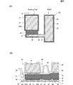
- FIG. 1A is a plan view of the semiconductor device according to the first embodiment
- FIG. 1B is a cross-sectional view taken along the line AA ′ in FIG. 1A
- FIG. 1C is a cross-sectional view of FIG.
- FIG. 6 is a cross-sectional view taken along the line BB ′. It is a result of the high-temperature, high-humidity bias test of the semiconductor device according to the first embodiment and the conventional semiconductor device.
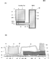
- FIG. 3A is a plan view of the semiconductor device according to the second embodiment
- FIG. 3B is a cross-sectional view taken along the line A-A ′ of FIG.
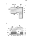
- FIG. 4A is a plan view of the semiconductor device according to the third embodiment
- FIG. 4B is a cross-sectional view taken along the line A-A ′ of FIG. 5A is a plan view illustrating an example of a conventional semiconductor device
- FIG. 5B is a cross-sectional view taken along the line A-A ′ in FIG. 5A.
- FIG. 1A is a plan view of the semiconductor device according to the first embodiment.
- FIG. 1B is a cross-sectional view taken along the line A-A ′ of FIG.
- FIG. 1C is a cross-sectional view taken along the line B-B ′ of FIG.
- the surface facing the upper side in FIG. 1B is referred to as the upper surface
- the surface facing the lower side is referred to as the lower surface. Note that in FIG. 1A, a part of the semiconductor device 1 is illustrated.
- the semiconductor device 1 includes a semiconductor substrate 11, surface electrodes 21 and 22, first wiring layers 31, 32, 33 and 34, insulating layers 41, 42 and 43, second wiring layers 51, 52 and 53, and a protective film 61. , 62, 63 and vias 71, 72, 73.
- the protective film 62 is a first protective film according to the first embodiment.
- the protective film 63 is a second protective film according to the first embodiment.
- the semiconductor device 1 is, for example, an MMIC chip.
- the semiconductor substrate 11 is, for example, a GaAs substrate. Although not shown, circuit elements such as transistors are formed on the upper surface of the semiconductor substrate 11.
- the surface electrodes 21 and 22 are in contact with the upper surface of the semiconductor substrate 11.
- the surface electrodes 21 and 22 are substantially rectangular flat plate conductors.
- the surface electrodes 21 and 22 are connected to each other and are electrically connected to each other.
- the surface electrodes 21 and 22 are connected to circuit elements formed on the upper surface of the semiconductor substrate 11.
- the first wiring layers 31 and 32 are formed on the upper surface of the semiconductor substrate 11 with the protective film 61 interposed therebetween.
- the first wiring layer 33 is formed on the upper surface of the surface electrode 21 through the via 72.
- the first wiring layer 34 is formed on the upper surface of the surface electrode 22 via the protective film 61.
- the first wiring layers 31, 32, and 33 are connected to each other and are electrically connected to each other.
- the first wiring layers 31 to 34 are substantially rectangular flat plate conductors.
- the insulating layer 41 is formed on the upper surface of the semiconductor substrate 11 via the protective films 61 and 62.
- the insulating layer 42 is formed on the upper surface of the first wiring layer 32 via the protective film 62.
- the insulating layer 43 is formed on the upper surface of the surface electrode 21 via the protective films 61 and 62.
- the insulating layers 41 and 42 are arranged away from the second wiring layer 51.
- the insulating layers 41 and 42 surround the second wiring layer 51 when viewed from the direction perpendicular to the upper surface of the semiconductor substrate 11.
- the insulating layer 43 is disposed between the first wiring layers 33 and 34.
- the insulating layers 41, 42, and 43 are formed so as to be connected together with other insulating layers not shown.
- the insulating layers 41, 42, 43 are made of, for example, a resin such as polyimide, which is a generally easily available material, and has a hygroscopic property.
- the second wiring layer 51 is formed on the upper surface of the first wiring layer 31 through the via 71.
- the second wiring layer 52 is formed on the upper surface of the first wiring layer 33 through the via 73 and is formed on the upper surface of the insulating layer 43.
- the second wiring layer 53 is formed on the upper surface of the first wiring layer 34 via the protective film 62.
- the second wiring layers 52 and 53 are connected to each other and are electrically connected to each other.
- the second wiring layer 51 is formed away from the second wiring layers 52 and 53.
- the second wiring layers 51, 52 and 53 are substantially rectangular flat conductors.
- the second wiring layers 51, 52, 53 are, for example, an alloy containing Au as a main component.
- the protective film 62 is formed so as to surround the second wiring layer 51 when viewed from a direction perpendicular to the upper surface of the semiconductor substrate 11.
- the protective film 63 is continuously formed on the surface of the semiconductor device 1 except for the upper surface of the second wiring layer 51.
- the protective films 61, 62, and 63 are, for example, silicon nitride films or silicon oxide films, and have moisture resistance and adhesion between the protective films.
- the groove 81 is formed by the side surface of the second wiring layer 51 and the side surface of the insulating layer 41.
- the groove 82 is formed by the side surface of the second wiring layer 51 and the side surface of the insulating layer 42.
- the protective films 62 and 63 are in contact with the bottom surfaces of the groove portions 81 and 82.
- the semiconductor device 1 is sealed with a mold resin or the like.
- the second wiring layer 51 is used as a bonding pad.
- the bonding pad is an electrode pad according to the first embodiment.
- the surface electrode 22, the first wiring layer 34, the second wiring layer 53, and the protective films 61 and 62 are used as MIMC.
- the bonding pad and the MIMC are connected by the surface electrode 21, the first wiring layers 31, 32, 33, the second wiring layer 52, and vias 71, 72, 73.
- the MIMC is connected to an external power source, an RF signal line, etc. by a bonding pad.
- the mold resin or the like for sealing the semiconductor device 1 generally has a hygroscopic property. For this reason, the moisture in the atmosphere reaches the surface of the bonding pad through the path R1.
- the adhesion between the second wiring layer 51 and the protective film 63 is not sufficient to prevent moisture from entering. Therefore, moisture that reaches the surface of the bonding pad enters the semiconductor device 1 through the path R2 between the second wiring layer 51 and the protective film 63.
- the protective films 62 and 63 have high moisture resistance. Further, the adhesion between the protective films 62 and 63 is sufficient to prevent moisture from entering. For this reason, the penetration of moisture into the insulating layers 41 and 42 is almost prevented in the region A1 where the protective films 62 and 63 abut.
- the region A2 corresponds to the edge of the MIMC electrode, and is where the electric field concentrates when a voltage is applied to the MIMC.
- the protective film 62 in the region A2 reacts with moisture by applying a voltage to the MIMC.
- a short-circuit portion is generated in the protective film 62, so that the MIMC characteristics are deteriorated.
- a discharge occurs between the second wiring layer 53 and the first wiring layer 34, and the MIMC is broken down.
- the intrusion of moisture is prevented in the region A1
- the moisture does not enter the insulating layers 41, 42, and 43. Therefore, it is possible to suppress the MIMC characteristic deterioration and hence the dielectric breakdown.
- the second wiring layer 51 is composed only of the bonding pad portion, the surface of the second wiring layer 51 can be flattened as compared with the structure in which the bonding pad and the wiring are formed simultaneously. Thereby, bonding conditions can be stabilized.
- the protective films 62 and 63 are preferably made of the same material. Thereby, the protective films 62 and 63 have high adhesiveness compared with different substances. Therefore, the moisture resistance of the semiconductor device 1 can be further improved.
- the bonding pad and the insulating layers 41 and 42 are preferably arranged as far apart as possible. Thereby, the area of the surface with which the protective films 62 and 63 abut is increased on the bottom surface of the groove portions 81 and 82. Therefore, it is possible to further suppress the intrusion of moisture from the peripheral portion of the bonding pad into the insulating layers 41, 42, and 43.
- the components of the semiconductor device 1 are not limited to the above.
- the wiring layer may be composed of three or more layers.
- FIG. 2 shows the results of the high-temperature and high-humidity bias test of the semiconductor device 1 according to the first embodiment and the semiconductor device 1P having the conventional configuration.
- the horizontal axis represents the test time
- the vertical axis represents the leakage current.
- the time until the leakage current rapidly increases is 3.5 times that of the conventional semiconductor device 1P. Therefore, the moisture resistance of the semiconductor device 1 according to the first embodiment is improved as compared with the semiconductor device 1P having the conventional configuration.
- FIG. 3A is a plan view of the semiconductor device according to the second embodiment
- FIG. 3B is a cross-sectional view taken along the line A-A ′ of FIG.
- the surface facing the upper side in FIG. 3B is referred to as an upper surface
- the surface facing the lower side is referred to as a lower surface.
- FIG. 3A illustrates a part of the semiconductor device 1A.
- the semiconductor device 1A according to the second embodiment includes a surface electrode 23A and a via 74A in addition to the configuration of the semiconductor device 1 according to the first embodiment.
- the surface electrode 23 ⁇ / b> A is formed so as to contact the upper surface of the semiconductor substrate 11.
- the first wiring layer 31 is formed on the surface electrode 23A via the via 74A.
- the bonding pad is formed on the semiconductor substrate 11 without the protective film 61, the shear strength of wire bonding and the like can be improved.
- the penetration of moisture into the insulating layers 41 and 42 is almost prevented in the region A1 where the protective films 62 and 63 are in contact. Therefore, as in the first embodiment, the moisture resistance of the semiconductor device 1A can be improved. Moreover, the effect of other 1st Embodiment can be acquired similarly.
- FIG. 4A is a plan view of the semiconductor device according to the third embodiment
- FIG. 4B is a cross-sectional view taken along the line A-A ′ of FIG.
- the surface facing the upper side in FIG. 4B will be referred to as the upper surface
- the surface facing the lower side will be referred to as the lower surface.
- FIG. 4A illustrates a part of the semiconductor device 1B.
- the semiconductor device 1B according to the third embodiment includes surface electrodes 23B and 24B and vias 74B in addition to the configuration of the semiconductor device 1 according to the first embodiment. Further, the semiconductor device 1B includes a first wiring layer 32B instead of the first wiring layers 31 and 32 according to the first embodiment.
- the surface electrodes 23B and 24B are formed so as to contact the upper surface of the semiconductor substrate 11.
- the first wiring layer 32B is formed on the upper surface of the surface electrode 24B via the via 74B, and is formed on the upper surface of the semiconductor substrate 11 via the protective film 61.
- the second wiring layer 51 is formed on the upper surface of the surface electrode 24 ⁇ / b> B through the via 71.
- the first wiring layer 32B and the second wiring layer 51 are connected by the surface electrodes 23B and 24B and vias 71 and 74B.
- the bonding pads and MIMC are connected to each other by the surface electrodes 21, 23B, 24B, the first wiring layers 32B, 33, the second wiring layer 52, and vias 71, 72, 73.
- the penetration of moisture into the insulating layers 41 and 42 is almost prevented in the region A1 where the protective films 62 and 63 are in contact. Therefore, the moisture resistance of the semiconductor device 1B can be improved as in the first embodiment. Moreover, the effect of other 1st Embodiment can be acquired similarly.
- the bonding pad is directly formed on the semiconductor substrate 11 via the via 71 and the surface electrode 23B, the shear strength of wire bonding and the like can be improved.
Landscapes
- Internal Circuitry In Semiconductor Integrated Circuit Devices (AREA)
Abstract
半導体装置(1)は、半導体基板(11)、配線層(51)、第1の保護膜(62)、絶縁層(41,42)、および第2の保護膜(63)を備える。配線層(51)は、半導体基板(11)上に形成され、ボンディングパッドとして使用される。第1の保護膜(62)は、ボンディングパッドを囲むように半導体基板(11)上に形成され、耐湿性を有する。絶縁層(41,42)は、第1の保護膜(62)上に形成され、吸湿性を有する。第2の保護膜(63)は、ボンディングパッド上と絶縁層(41,42)上と第1の保護膜(62)上とに連続的に形成され、ボンディングパッドの中心部で開口する。第2の保護膜(63)は、耐湿性を有し、第1の保護膜(62)と密着性を有する。ボンディングパッドの側面と絶縁層(41,42)の側面とにより溝部(81,82)が形成され、第1の保護膜(61)と第2の保護膜(62)は、溝部(81,82)の底面で当接する。
Description
本発明は、電極パッドを備える半導体装置に関する。
半導体装置は、半導体基板および半導体基板に形成された多数の回路素子から構成され、様々な電子機器に内蔵されている。半導体装置は、大気中の水分から回路素子を保護するため、耐湿性を有するように設計されている。
耐湿性を考慮した従来の半導体装置として、例えば、特許文献1に示すような構造のものがある。特許文献1に記載の半導体装置は、半導体基板、積層体、保護溝部、ボンディングパッドおよび保護膜を備える。積層体は、半導体基板上に形成されている。積層体の一方端は、スクライブされ、大気に露出している。保護溝部は、半導体基板表面が露出されるように、積層体に形成されている。ボンディングパッドは、積層体上に形成されている。保護膜は、ボンディングパッドがある部分を除き、積層体の上面ならびに保護溝部の側壁面および底面を覆っている。
大気中の水分は、積層体の端面から積層体内に侵入する。しかし、保護溝部より先への侵入は、保護溝部に設けられた保護膜により阻止される。
また、耐湿性を考慮した従来の半導体装置として、図5に示すような構造のものがある。図5(A)は、従来の半導体装置の一例を示す平面図である。図5(B)は、図5(A)のA-A’断面図である。以下では、図5(B)の上側を向いている面を上面、下側を向いている面を下面と称して説明する。なお、図5(A)では、半導体装置1Pの一部を図示している。
半導体装置1Pは、半導体基板11と表面電極21P,22,23Pと第1の配線層31P,34と絶縁層41P,42Pと第2の配線層51P,52P,53と保護膜61,62,63とビア71,74Pとを有する。
表面電極21P,22,23Pは半導体基板11の上面に当接している。表面電極21P,22,23Pは、連接して形成され、互いに導通している。
第1の配線層31Pは、ビア74Pを介して表面電極23Pの上面に形成されている。第1の配線層34は、保護膜61を介して表面電極22の上面に形成されている。
絶縁層41Pは、保護膜61,62を介して半導体基板11の上面に形成されている。絶縁層42Pは、保護膜61,62を介して表面電極21Pの上面に形成され、第1の配線層31P,34の間に位置している。絶縁層41P,42Pは、図示されていない他の絶縁層とともに連接して形成されている。絶縁層41P,42Pは、吸湿性を有する。
第2の配線層51Pは、ビア71を介して第1の配線層31Pの上面に形成されている。第2の配線層52Pは、絶縁層42Pの上面に形成されている。第2の配線層53は、保護膜62を介して第1の配線層34の上面に形成されている。第2の配線層51P,52P,53は、連接して形成され、互いに導通している。
保護膜63は、第2の配線層51Pの上面を除いて、半導体装置1Pの表面に形成されている。保護膜61,62,63は、耐湿性と保護膜同士の密着性とを有する。
半導体装置1Pは、モールド樹脂等により封止されている。
第2の配線層51Pは、ボンディングパッドとして使用される。表面電極22と第1の配線層34と第2の配線層53と保護膜61,62とは、MIMC(Metal-Insulator-Metal Capacitor)として使用される。ボンディングパッドと当該MIMCとは、表面電極21P,23Pと第1の配線層31Pと第2の配線層52Pとビア71,74Pとにより接続されている。
当該MIMCは、外部電源やRF信号ライン等にボンディングパッドにより接続される。
特許文献1に記載の半導体装置の構成を用いた場合、積層体の端面からの水分の侵入を保護膜により阻止することができる。しかし、保護膜がボンディングパッドの上面を覆っていないため、ボンディングパッド周辺部からの水分の侵入を阻止することができない。積層体内に形成された回路素子の特性は、侵入した水分により劣化するおそれがある。
半導体装置を封止するモールド樹脂等は、一般的に吸湿性を有する。このため、図5(B)に示す半導体装置1Pでは、大気中の水分は、経路R1を通ってボンディングパッドの表面まで達する。
第2の配線層51Pと保護膜63との密着性は、水分の侵入を阻止するために十分でない。このため、経路R1を進んだ水分は、第2の配線層51Pと保護膜63との間の経路R2を通って、半導体装置1P内に侵入する。
絶縁層41P,42Pは、吸湿性を有する材料で形成されている。このため、経路R2まで進んだ水分は、互いにつながっている絶縁層41P,42P内の経路R3を通って、領域A2に侵入する。
領域A2は、MIMCの電極のエッジに相当し、MIMCに電圧を印加したとき電界が集中する箇所である。水分が領域A2に侵入した場合、領域A2にある保護膜62は、MIMCへの電圧印加により水分と反応する。これにより、短絡箇所が保護膜62に発生するため、MIMCの特性は、劣化する。
本発明の目的は、半導体装置の耐湿性を向上させることにある。
本発明に係る半導体装置は、以下のように構成される。本発明に係る半導体装置は、半導体基板、配線層、第1の保護膜、絶縁層および第2の保護膜を備える。配線層は、半導体基板上に形成され、電極パッドとして使用される。第1の保護膜は、半導体基板の主面に垂直な方向から見て電極パッドを囲むように、半導体基板上に形成され、耐湿性を有する。絶縁層は、電極パッドから離れて第1の保護膜上に形成され、吸湿性を有する。第2の保護膜は、電極パッド上と絶縁層上と第1の保護膜上とに連続的に形成され、電極パッドの中心部で開口する。第2の保護膜は、耐湿性を有し、第1の保護膜と密着性を有する。電極パッドの側面と絶縁層の側面とにより溝部が形成され、第1の保護膜と第2の保護膜は、溝部の底面で当接する。
この構成では、第1の保護膜と第2の保護膜とが連続して当接していることにより、水分の侵入を防止する壁が形成されている。したがって、電極パッド周辺部から吸湿性を有する絶縁層への水分の侵入を抑制することができる。これにより、半導体装置の耐湿性を向上させることができる。
本発明に係る半導体装置では、第1の保護膜と第2の保護膜とは、好ましくは、同一の物質から作られる。この構成では、第1の保護膜と第2の保護膜とは、異なる物質同士に比べて高い密着性を有する。したがって、半導体装置の耐湿性をさらに向上させることができる。
本発明に係る半導体装置は、以下のように構成されてもよい。配線層は、第1の配線層と第2の配線層とを備える。第1の配線層は、半導体基板上に形成され、電極パッドに接続された配線として使用される。第2の配線層は、第1の配線層上に形成され、電極パッドとして使用される。第1の保護膜の一部は、第1の配線層を介して半導体基板上に形成される。
この構成では、第2の配線層の表面を平坦にすることができる。これにより、ボンディング条件を安定させることができる。
本発明に係る半導体装置では、以下のように構成されてもよい。本発明に係る半導体装置は、半導体基板上に当接した表面電極を備える。第1の配線層は、表面電極を介して半導体基板上に形成される。
この構成では、ワイヤボンディングのシェア強度等を向上させることができる。
本発明によると、電極パッド周辺部から吸湿性を有する絶縁層への水分の侵入を抑制することができる。これにより、半導体装置の耐湿性を向上させることができる。
本発明の第1の実施形態に係る半導体装置について説明する。図1(A)は、第1の実施形態に係る半導体装置の平面図である。図1(B)は、図1(A)のA-A’断面図である。図1(C)は、図1(A)のB-B’矢視断面図である。以下では、図1(B)の上側を向いている面を上面、下側を向いている面を下面と称して説明する。なお、図1(A)では、半導体装置1の一部を図示している。
半導体装置1は、半導体基板11、表面電極21,22、第1の配線層31,32,33,34、絶縁層41,42,43、第2の配線層51,52,53、保護膜61,62,63およびビア71,72,73を有する。保護膜62は、第1の実施形態に係る第1の保護膜である。保護膜63は、第1の実施形態に係る第2の保護膜である。半導体装置1は、例えば、MMICチップである。
半導体基板11は、例えば、GaAs基板等である。なお、図示されていないが、トランジスタ等の回路素子が半導体基板11の上面に形成されている。
表面電極21,22は、半導体基板11の上面に当接している。表面電極21,22は、略矩形状平板の導体である。表面電極21,22は、連接して形成され、互いに導通している。表面電極21,22は、半導体基板11の上面に形成された回路素子に接続されている。
第1の配線層31,32は、保護膜61を介して半導体基板11の上面に形成されている。第1の配線層33は、ビア72を介して表面電極21の上面に形成されている。第1の配線層34は、保護膜61を介して表面電極22の上面に形成されている。第1の配線層31,32,33は、連接して形成され、互いに導通している。第1の配線層31ないし34は、略矩形状平板の導体である。
絶縁層41は、保護膜61,62を介して半導体基板11の上面に形成されている。絶縁層42は、保護膜62を介して第1の配線層32の上面に形成されている。絶縁層43は、保護膜61,62を介して表面電極21の上面に形成されている。
絶縁層41,42は、第2の配線層51から離れて配置されている。絶縁層41,42は、半導体基板11の上面に垂直な方向から見て、第2の配線層51を囲んでいる。絶縁層43は、第1の配線層33,34の間に配置されている。絶縁層41,42,43は、図示されていない他の絶縁層とともに連接して形成されている。絶縁層41,42,43は、例えば、一般的に入手容易な材料であるポリイミド等の樹脂から作られ、吸湿性を有する。
第2の配線層51は、ビア71を介して第1の配線層31の上面に形成されている。第2の配線層52は、ビア73を介して第1の配線層33の上面に形成されるとともに、絶縁層43の上面に形成される。第2の配線層53は、保護膜62を介して第1の配線層34の上面に形成されている。第2の配線層52,53は、連接して形成され、互いに導通している。第2の配線層51は第2の配線層52,53から離れて形成されている。第2の配線層51,52,53は、略矩形平板状の導体である。第2の配線層51,52,53は、例えば、Au等を主成分とする合金である。
保護膜62は、半導体基板11の上面に垂直な方向から見て、第2の配線層51を囲むように形成されている。保護膜63は、第2の配線層51の上面を除いて、半導体装置1の表面に連続的に形成されている。保護膜61,62,63は、例えば、シリコン窒化膜またはシリコン酸化膜等であり、耐湿性と保護膜同士の密着性とを有する。
溝部81は、第2の配線層51の側面と絶縁層41の側面とにより形成されている。溝部82は、第2の配線層51の側面と絶縁層42の側面とにより形成されている。保護膜62,63は、溝部81,82の底面で当接している。
半導体装置1は、モールド樹脂等により封止されている。
第2の配線層51は、ボンディングパッドとして使用される。ボンディングパッドは、第1の実施形態に係る電極パッドである。表面電極22と第1の配線層34と第2の配線層53と保護膜61,62とは、MIMCとして使用される。ボンディングパッドと当該MIMCとは、表面電極21と第1の配線層31,32,33と第2の配線層52とビア71,72,73により接続されている。
当該MIMCは、外部電源やRF信号ライン等にボンディングパッドにより接続される。
半導体装置1を封止するモールド樹脂等は、一般的に吸湿性を有する。このため、大気中の水分は、経路R1を通ってボンディングパッドの表面まで達する。
第2の配線層51と保護膜63との密着性は、水分の侵入を阻止するために十分でない。このため、ボンディングパッドの表面まで達した水分は、第2の配線層51と保護膜63との間の経路R2を通って、半導体装置1内に侵入する。
保護膜62,63は、高い耐湿性を有する。また、保護膜62,63の密着性は、水分の侵入を阻止するために十分である。このため、水分が絶縁層41,42に侵入することは、保護膜62,63が当接する領域A1でほとんど阻止される。
これにより、ボンディングパッドの周辺部から絶縁層41,42,43への水分の侵入を抑制することができる。したがって、半導体装置1の耐湿性を向上させることができる。
また、領域A2は、MIMCの電極のエッジに相当し、MIMCに電圧を印加したとき電界が集中する箇所である。水分が領域A2に侵入した場合、領域A2にある保護膜62は、MIMCへの電圧印加により水分と反応する。これにより、短絡箇所が保護膜62に発生するため、MIMCの特性は劣化し、ひいては、第2の配線層53と第1の配線層34との間で放電が発生し、MIMCが絶縁破壊される。しかし、水分の侵入が領域A1で阻止されるので、絶縁層41,42,43へ水分が侵入することはない。したがって、MIMCの特性劣化ひいては絶縁破壊を抑制することができる。
また、第2の配線層51がボンディングパッド部分のみからなるので、ボンディングパッドと配線とが同時に形成される構造に比べて第2の配線層51の表面を平坦にすることができる。これにより、ボンディング条件を安定させることができる。
また、保護膜62,63は、好ましくは、同一の物質から作られる。これにより、保護膜62,63は、異なる物質同士に比べて高い密着性を有する。したがって、半導体装置1の耐湿性をさらに向上させることができる。
なお、ボンディングパッドと絶縁層41,42とは、好ましくは、可能な限り離して配置される。これにより、保護膜62,63が当接する面の面積は、溝部81,82の底面で大きくなる。したがって、ボンディングパッドの周辺部から絶縁層41,42,43への水分の侵入をさらに抑制することができる。
また、半導体装置1の構成要素は、上記に限定されない。例えば、配線層は、3以上の層から構成されてもよい。
図2は、第1の実施形態に係る半導体装置1および従来構成の半導体装置1Pの高温高湿バイアス試験の結果である。図2では、横軸は試験時間、縦軸はリーク電流である。図2に示すように、第1の実施形態に係る半導体装置1では、リーク電流が急増するまでの時間は、従来構成の半導体装置1Pの3.5倍となっている。したがって、第1の実施形態に係る半導体装置1の耐湿性は、従来構成の半導体装置1Pに比べて向上している。
本発明の第2の実施形態に係る半導体装置について説明する。図3(A)は第2の実施形態に係る半導体装置の平面図、図3(B)は図3(A)のA-A’矢視断面図である。以下では、図3(B)の上側を向いている面を上面、下側を向いている面を下面と称して説明する。また、第1の実施形態と異なる点を説明する。なお、図3(A)では、半導体装置1Aの一部を図示している。
第2の実施形態に係る半導体装置1Aは、第1の実施形態に係る半導体装置1の構成に加えて、表面電極23Aとビア74Aとを備える。
表面電極23Aは、半導体基板11の上面に当接するように形成されている。第1の配線層31は、ビア74Aを介して表面電極23A上に形成されている。
第2の実施形態によると、ボンディングパッドが保護膜61を介さずに半導体基板11上に形成されるため、ワイヤボンディングのシェア強度等を向上させることができる。
また、水分が絶縁層41,42に侵入することは、保護膜62,63が当接している領域A1でほとんど阻止される。したがって、第1の実施形態と同様に、半導体装置1Aの耐湿性を向上させることができる。また、他の第1の実施形態の効果を同様に得ることができる。
本発明の第3の実施形態に係る半導体装置について説明する。図4(A)は第3の実施形態に係る半導体装置の平面図、図4(B)は図4(A)のA-A’矢視断面図である。以下では、図4(B)の上側を向いている面を上面、下側を向いている面を下面と称して説明する。また、第1の実施形態と異なる点を説明する。なお、図4(A)では、半導体装置1Bの一部を図示している。
第3の実施形態に係る半導体装置1Bは、第1の実施形態に係る半導体装置1の構成に加えて、表面電極23B,24Bとビア74Bとを備える。また、半導体装置1Bは、第1の実施形態に係る第1の配線層31,32に代えて、第1の配線層32Bを備える。
表面電極23B,24Bは、半導体基板11の上面に当接するように形成されている。第1の配線層32Bは、ビア74Bを介して表面電極24Bの上面に形成されるとともに、保護膜61を介して半導体基板11の上面に形成されている。第2の配線層51は、ビア71を介して表面電極24Bの上面に形成されている。第1の配線層32Bと第2の配線層51とは、表面電極23B,24Bとビア71,74Bとにより接続されている。
ボンディングパッドとMIMCとは、表面電極21,23B,24Bと第1の配線層32B,33と第2の配線層52とビア71,72,73により接続されている。
第3の実施形態によると、水分が絶縁層41,42に侵入することは、保護膜62,63が当接している領域A1でほとんど阻止される。したがって、第1の実施形態と同様に、半導体装置1Bの耐湿性を向上させることができる。また、他の第1の実施形態の効果を同様に得ることができる。
また、第3の実施形態によると、ボンディングパッドは、ビア71と表面電極23Bとを介して直接半導体基板11上に形成されるため、ワイヤボンディングのシェア強度等を向上させることができる。
1,1A,1B,1P 半導体装置
11 半導体基板
21,22,23A,23B,24B,21P,23P 表面電極
31,32,33,34,32B,31P 第1の配線層
41,42,43,41P,42P 絶縁層
51,52,53,51P,52P 第2の配線層
61,62,63 保護膜
71,72,73,74A,74B,74P ビア
11 半導体基板
21,22,23A,23B,24B,21P,23P 表面電極
31,32,33,34,32B,31P 第1の配線層
41,42,43,41P,42P 絶縁層
51,52,53,51P,52P 第2の配線層
61,62,63 保護膜
71,72,73,74A,74B,74P ビア
Claims (8)
- 半導体基板と、
前記半導体基板上に形成され、電極パッドとして使用される配線層と、
前記半導体基板の主面に垂直な方向から見て前記電極パッドを囲むように、前記半導体基板上に形成され、耐湿性を有する第1の保護膜と、
前記電極パッドから離れて前記第1の保護膜上に形成され、吸湿性を有する絶縁層と、
前記電極パッド上と前記絶縁層上と前記第1の保護膜上とに連続的に形成され、前記電極パッドの中心部で開口し、耐湿性を有し、第1の保護膜と密着性を有する第2の保護膜とを備え、
前記電極パッドの側面と前記絶縁層の側面とにより溝部が形成され、前記第1の保護膜と前記第2の保護膜は、前記溝部の底面で当接することを特徴とする半導体装置。 - 前記第1の保護膜と前記第2の保護膜とは、同一の物質から作られることを特徴とする請求項1に記載の半導体装置。
- 前記配線層は、第1の配線層と第2の配線層とを備え、
前記第1の配線層は、前記半導体基板上に形成され、前記電極パッドに接続された配線として使用され、
前記第2の配線層は、前記第1の配線層上に形成され、前記電極パッドとして使用され、
前記第1の保護膜の一部は、前記第1の配線層を介して前記半導体基板上に形成されることを特徴とする請求項1または2に記載の半導体装置。 - 前記半導体基板上に当接した表面電極を備え、
前記第1の配線層は、前記表面電極を介して前記半導体基板上に形成されることを特徴とする請求項3に記載の半導体装置。 - 前記半導体基板上に当接した表面電極を備え、
前記配線層は、前記表面電極を介して前記半導体基板上に形成され、
前記表面電極は、前記電極パッドに接続された配線として使用され、
前記第1の保護膜の一部は、前記表面電極を介して前記半導体基板上に形成されることを特徴とする請求項1または2に記載の半導体装置。 - 前記電極パッドは、ボンディングパッドであることを特徴とする請求項1ないし5のいずれかに記載の半導体装置。
- 前記第1の保護膜と前記第2の保護膜とは、シリコン窒化膜またはシリコン酸化膜であることを特徴とする請求項1ないし6のいずれかに記載の半導体装置。
- 前記絶縁層は、樹脂から作られることを特徴とする請求項1ないし7のいずれかに記載の半導体装置。
Applications Claiming Priority (2)
| Application Number | Priority Date | Filing Date | Title |
|---|---|---|---|
| JP2013-018006 | 2013-02-01 | ||
| JP2013018006 | 2013-02-01 |
Publications (1)
| Publication Number | Publication Date |
|---|---|
| WO2014119045A1 true WO2014119045A1 (ja) | 2014-08-07 |
Family
ID=51261781
Family Applications (1)
| Application Number | Title | Priority Date | Filing Date |
|---|---|---|---|
| PCT/JP2013/076771 Ceased WO2014119045A1 (ja) | 2013-02-01 | 2013-10-02 | 半導体装置 |
Country Status (2)
| Country | Link |
|---|---|
| TW (1) | TW201432864A (ja) |
| WO (1) | WO2014119045A1 (ja) |
Citations (9)
| Publication number | Priority date | Publication date | Assignee | Title |
|---|---|---|---|---|
| JPS6164147A (ja) * | 1984-09-05 | 1986-04-02 | Nec Corp | 半導体装置 |
| JPS6367751A (ja) * | 1986-09-09 | 1988-03-26 | Mitsubishi Electric Corp | 半導体装置 |
| JPS63308924A (ja) * | 1987-06-11 | 1988-12-16 | Nec Corp | 半導体装置 |
| JPH03191526A (ja) * | 1989-12-20 | 1991-08-21 | Nec Corp | 集積回路 |
| JPH0823007A (ja) * | 1994-07-08 | 1996-01-23 | Nippon Precision Circuits Kk | 半導体集積回路装置および半導体集積回路装置の製造方法 |
| JP2000357743A (ja) * | 1999-06-16 | 2000-12-26 | Matsushita Electronics Industry Corp | 半導体装置およびその製造方法 |
| JP2008034472A (ja) * | 2006-07-26 | 2008-02-14 | Sony Corp | 半導体装置及びその製造方法 |
| JP2008091454A (ja) * | 2006-09-29 | 2008-04-17 | Rohm Co Ltd | 半導体装置及び半導体装置の製造方法 |
| JP2010287750A (ja) * | 2009-06-12 | 2010-12-24 | Sanyo Electric Co Ltd | 半導体装置及びその製造方法 |
-
2013
- 2013-09-12 TW TW102132956A patent/TW201432864A/zh unknown
- 2013-10-02 WO PCT/JP2013/076771 patent/WO2014119045A1/ja not_active Ceased
Patent Citations (9)
| Publication number | Priority date | Publication date | Assignee | Title |
|---|---|---|---|---|
| JPS6164147A (ja) * | 1984-09-05 | 1986-04-02 | Nec Corp | 半導体装置 |
| JPS6367751A (ja) * | 1986-09-09 | 1988-03-26 | Mitsubishi Electric Corp | 半導体装置 |
| JPS63308924A (ja) * | 1987-06-11 | 1988-12-16 | Nec Corp | 半導体装置 |
| JPH03191526A (ja) * | 1989-12-20 | 1991-08-21 | Nec Corp | 集積回路 |
| JPH0823007A (ja) * | 1994-07-08 | 1996-01-23 | Nippon Precision Circuits Kk | 半導体集積回路装置および半導体集積回路装置の製造方法 |
| JP2000357743A (ja) * | 1999-06-16 | 2000-12-26 | Matsushita Electronics Industry Corp | 半導体装置およびその製造方法 |
| JP2008034472A (ja) * | 2006-07-26 | 2008-02-14 | Sony Corp | 半導体装置及びその製造方法 |
| JP2008091454A (ja) * | 2006-09-29 | 2008-04-17 | Rohm Co Ltd | 半導体装置及び半導体装置の製造方法 |
| JP2010287750A (ja) * | 2009-06-12 | 2010-12-24 | Sanyo Electric Co Ltd | 半導体装置及びその製造方法 |
Also Published As
| Publication number | Publication date |
|---|---|
| TW201432864A (zh) | 2014-08-16 |
Similar Documents
| Publication | Publication Date | Title |
|---|---|---|
| US10056319B2 (en) | Power module package having patterned insulation metal substrate | |
| CN110326073B (zh) | 电容器 | |
| US10888941B2 (en) | Power semiconductor module | |
| US20120175755A1 (en) | Semiconductor device including a heat spreader | |
| US8963315B2 (en) | Semiconductor device with surface electrodes | |
| US10727209B2 (en) | Semiconductor device and semiconductor element with improved yield | |
| CN106449614B (zh) | 半导体装置 | |
| US20170092574A1 (en) | Method for manufacture a power electronic switching device and power electronic switching device | |
| NL2021292B1 (en) | Electronic module | |
| JPWO2021049039A1 (ja) | 半導体装置 | |
| CN107170732A (zh) | 半导体装置 | |
| CN107026129B (zh) | 半导体装置 | |
| TWI567907B (zh) | 半導體裝置 | |
| JP6095303B2 (ja) | 半導体装置および半導体装置の製造方法 | |
| US9905439B2 (en) | Power module package having patterned insulation metal substrate | |
| CN114080672A (zh) | 半导体装置 | |
| US11749731B2 (en) | Semiconductor device | |
| JP7790601B2 (ja) | 半導体モジュール | |
| US9865531B2 (en) | Power module package having patterned insulation metal substrate | |
| US11004815B2 (en) | Semiconductor device | |
| WO2014119045A1 (ja) | 半導体装置 | |
| WO2019171795A1 (ja) | 半導体モジュール | |
| US10134661B2 (en) | Semiconductor device | |
| CN113841233A (zh) | 半导体模组 | |
| WO2023090137A1 (ja) | 半導体素子および半導体装置 |
Legal Events
| Date | Code | Title | Description |
|---|---|---|---|
| 121 | Ep: the epo has been informed by wipo that ep was designated in this application |
Ref document number: 13874141 Country of ref document: EP Kind code of ref document: A1 |
|
| NENP | Non-entry into the national phase |
Ref country code: DE |
|
| 122 | Ep: pct application non-entry in european phase |
Ref document number: 13874141 Country of ref document: EP Kind code of ref document: A1 |
|
| NENP | Non-entry into the national phase |
Ref country code: JP |