WO2014115840A1 - Dispositif récepteur optique et procédé de réduction du glissement de cycle de phase - Google Patents
Dispositif récepteur optique et procédé de réduction du glissement de cycle de phase Download PDFInfo
- Publication number
- WO2014115840A1 WO2014115840A1 PCT/JP2014/051501 JP2014051501W WO2014115840A1 WO 2014115840 A1 WO2014115840 A1 WO 2014115840A1 JP 2014051501 W JP2014051501 W JP 2014051501W WO 2014115840 A1 WO2014115840 A1 WO 2014115840A1
- Authority
- WO
- WIPO (PCT)
- Prior art keywords
- phase
- circuit
- symbol
- unit
- compensation
- Prior art date
Links
Images


Classifications
-
- H—ELECTRICITY
- H04—ELECTRIC COMMUNICATION TECHNIQUE
- H04B—TRANSMISSION
- H04B10/00—Transmission systems employing electromagnetic waves other than radio-waves, e.g. infrared, visible or ultraviolet light, or employing corpuscular radiation, e.g. quantum communication
- H04B10/60—Receivers
- H04B10/61—Coherent receivers
- H04B10/616—Details of the electronic signal processing in coherent optical receivers
- H04B10/6165—Estimation of the phase of the received optical signal, phase error estimation or phase error correction
-
- H—ELECTRICITY
- H04—ELECTRIC COMMUNICATION TECHNIQUE
- H04L—TRANSMISSION OF DIGITAL INFORMATION, e.g. TELEGRAPHIC COMMUNICATION
- H04L27/00—Modulated-carrier systems
- H04L27/02—Amplitude-modulated carrier systems, e.g. using on-off keying; Single sideband or vestigial sideband modulation
- H04L27/06—Demodulator circuits; Receiver circuits
- H04L27/066—Carrier recovery circuits
-
- H—ELECTRICITY
- H04—ELECTRIC COMMUNICATION TECHNIQUE
- H04L—TRANSMISSION OF DIGITAL INFORMATION, e.g. TELEGRAPHIC COMMUNICATION
- H04L27/00—Modulated-carrier systems
- H04L27/32—Carrier systems characterised by combinations of two or more of the types covered by groups H04L27/02, H04L27/10, H04L27/18 or H04L27/26
- H04L27/34—Amplitude- and phase-modulated carrier systems, e.g. quadrature-amplitude modulated carrier systems
- H04L27/38—Demodulator circuits; Receiver circuits
- H04L27/389—Demodulator circuits; Receiver circuits with separate demodulation for the phase and amplitude components
-
- H—ELECTRICITY
- H04—ELECTRIC COMMUNICATION TECHNIQUE
- H04L—TRANSMISSION OF DIGITAL INFORMATION, e.g. TELEGRAPHIC COMMUNICATION
- H04L7/00—Arrangements for synchronising receiver with transmitter
- H04L7/0016—Arrangements for synchronising receiver with transmitter correction of synchronization errors
- H04L7/0033—Correction by delay
- H04L7/0041—Delay of data signal
-
- H—ELECTRICITY
- H04—ELECTRIC COMMUNICATION TECHNIQUE
- H04L—TRANSMISSION OF DIGITAL INFORMATION, e.g. TELEGRAPHIC COMMUNICATION
- H04L7/00—Arrangements for synchronising receiver with transmitter
- H04L7/0075—Arrangements for synchronising receiver with transmitter with photonic or optical means
Definitions
- the present invention relates to a communication system and relates to a technique for reducing the occurrence of cycle slip in a carrier synchronization circuit.
- the backbone optical transmission system is required to economically accommodate high-speed client signals and transmit large amounts of information.
- a digital coherent transmission method combining coherent detection and digital signal processing has been studied from the viewpoint of improving frequency utilization efficiency, and high-speed and large-capacity information can be obtained by wavelength multiplexing transmission using the transmission method. Realization of transmission is expected.
- carrier phase synchronization is established by digital signal processing.
- Various algorithms and implementation methods have been studied for the configuration of the carrier phase synchronization circuit (CPR: Carrier Phase Recovery) in consideration of the circuit scale and modulation format.
- phase noise due to the line width of the laser used at the transmission / reception end
- frequency offset due to the frequency of the laser at the transmission / reception end
- phase noise due to the nonlinear optical effect.
- Non-patent Document 1 there is a Viterbi / Viterbi algorithm (Non-patent Document 1) as an algorithm for performing carrier phase synchronization blindly on the receiving side.
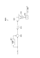
- FIG. 38 is a block diagram showing a configuration of a carrier phase synchronization circuit (CPR) to which the Viterbi / Viterbi algorithm is applied.
- CPR carrier phase synchronization circuit
- QPSK Quadrature Phase Shift Keying
- M 4
- the input symbol is represented as a complex value having an in-phase component I and a quadrature component Q.
- the CPR includes a carrier phase estimation unit 150 and a carrier phase compensation unit 160.
- the carrier phase estimation unit 150 includes an M-th power circuit 151, an averaging circuit 152, an angle calculation circuit 153, an unwrap circuit (not shown), a division circuit 154, and a complex number calculation circuit 155.
- the carrier phase compensation unit 160 includes a delay circuit 161 and a multiplication circuit 162.
- k is time
- w k additive noise
- ⁇ k is phase noise.
- the Viterbi Viterbi algorithm the modulation scheme by assuming M-PSK (M-ary Phase Shift Keying), A k is a constant, theta k utilizes can be expressed as 2 ⁇ mk / M. However, mk is an integer from 0 to M-1.
- Input symbols r k is input to the delay circuit 161 and the M-th power circuit 151.
- the M-th power circuit 151 raises the input symbol to the Mth power.
- w k ⁇ 0 is obtained by calculating the M-th power of the input symbol, the output is expressed by the following equation (2).
- the output of the M-th power circuit 151 is input to the averaging circuit 152 to reduce the influence of noise.
- the averaging circuit 152 adds the M-th power value of the input symbol calculated by the M-th power circuit 151 on the complex plane for every L averaging window widths including the M-th power value of the preceding and following input symbols. Averaging to reduce noise components.
- the output of the averaging circuit 152 is input to the angle calculation circuit 153.
- the angle calculation circuit 153 calculates the deflection angle of the symbol (complex number) averaged by the averaging circuit 152. If the noise is sufficiently reduced by the averaging circuit 152, the output of the angle calculation circuit 153 is M ⁇ k. As a calculation method, for example, the in-phase component (I) and the quadrature component (Q) of the output of the averaging circuit 152 are calculated, and arctan (Q / I) is calculated to convert the symbol into an angle.
- the unwrap circuit corrects the arbitraryness (360 ° ⁇ n, where n is an integer) remaining at the angle calculated by the angle calculation circuit 153. Specifically, the unwrap circuit corrects the angle so that the difference between the angle with respect to the previous input symbol and the current angle becomes small.
- the division circuit 154 multiplies the angle corrected in the unwrap circuit by (1 / M) and calculates the carrier phase estimation value.
- the complex number calculation circuit 155 calculates a complex number of size 1 with the carrier phase estimation value calculated by the division circuit 154 as an argument, and outputs the complex number to the multiplication circuit 162.
- the delay circuit 161 gives a delay corresponding to the time required for the calculation from the M-th power circuit 151 to the complex number calculation circuit 155 to the input symbol, and the input symbol is a multiplication circuit at the same timing as the complex number of size 1 corresponding to the input symbol. It outputs to 162.
- the multiplication circuit 162 multiplies the input symbol delayed by the delay circuit 161 by the complex number calculated by the complex number calculation circuit 155, and synchronizes with the carrier phase of the input symbol.
- the carrier phase estimation value estimated by the above algorithm can be estimated only in the range from 0 degrees to 90 degrees because the symbol phase is quadrupled (in the case of QPSK). Therefore, there are four possible estimation results included in any angle of 0 to 90 degrees, 90 to 180 degrees, 180 to 270 degrees, and 270 to 360 degrees, and the input symbol It is not possible to correctly estimate from four ways. Even if the correct phase shift amount is known as the initial value and the carrier phase estimation can be performed continuously for each symbol, if the interference due to large noise or nonlinear optical effects is suddenly added in the phase direction, the estimation is performed. An incorrect discontinuity occurs in the phase amount. When such a discontinuity occurs, carrier phase estimation cannot be performed correctly for subsequent input symbols. Such a phenomenon is known as phase cycle slip.
- a differential coding method and a correction method using a pilot symbol are considered to be effective.
- the phase difference between adjacent symbols is transmitted by an optical phase modulation signal, so that even if a phase cycle slip occurs, the influence can be limited to the bit error in the preceding and succeeding symbols.
- the bit error rate is doubled. This drawback has the problem that the signal-to-noise power ratio of the transmission line required to establish reliable communication using forward error correction technology is increased by about 1.11 to 1.4 dB.
- the correction method using a pilot symbol is a method for detecting and correcting a phase cycle slip by transmitting a known signal pattern.
- a phase cycle slip occurs, a burst error occurs until the absolute phase is synchronized again using a known signal pattern. If the cycle for inserting the known signal pattern is shortened in order to shorten the period in which the burst error occurs, there is a problem that overhead is increased and transmission efficiency is lowered.
- the present invention has been made in view of the above problems, and an object of the present invention is to provide a phase cycle capable of reducing the frequency of occurrence of phase cycle slip without increasing the bit error rate or reducing the transmission efficiency. It is an object of the present invention to provide a slip reduction system and a phase cycle slip reduction method.
- one embodiment of the present invention receives an optical signal generated from an electrical signal modulated using phase modulation or quadrature amplitude modulation, and electrically receives the received optical signal using coherent detection.
- a phase cycle slip reduction system that performs phase compensation on a received signal obtained by converting a signal into an electric signal and converting the electric signal into a digital signal, gain adjustment is performed by multiplying and multiplying the amplitude and phase of the CPR input symbol by multiplication and power
- a slip determination unit that determines the phase cycle slip using the carrier phase estimation value output from the carrier phase estimation unit, and compensates for the phase cycle slip based on the determination result of the phase cycle slip determination unit It is a phase cycle slip reduction system provided with a slip compensation part.
- the phase cycle slip determination / compensation unit can detect and compensate for the phase cycle slip to reduce the frequency of the phase cycle slip. Furthermore, by improving the estimation accuracy of the carrier phase estimation value of the carrier phase estimation unit by the gain adjustment circuit, it is possible to improve the detection accuracy of the phase cycle slip determination / compensation unit and further reduce the frequency of the phase cycle slip. it can. As a result, the phase can be accurately estimated without transmitting symbols that have been processed in advance, so that the frequency of occurrence of phase cycle slips can be reduced without increasing the bit error rate or reducing the transmission efficiency. it can.
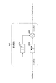
- FIG. 1 is a block diagram showing a carrier phase synchronization circuit (CPR) according to a first embodiment of the present invention.
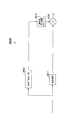
- FIG. 2 is a block diagram showing a gain adjustment circuit shown in FIG. 1. It is a graph which shows the reduction effect of the phase cycle slip ratio of the embodiment of the present invention. It is a block diagram which shows the receiver which concerns on the 2nd Embodiment of this invention. It is a block diagram which shows the phase compensation circuit which concerns on the 3rd Embodiment of this invention. It is a block diagram which shows the structure of the phase compensation circuit which concerns on the 4th Embodiment of this invention. It is a graph which shows an example of the estimation error phase which the carrier phase estimation part shown by FIG. 6 outputs.
- CPR carrier phase synchronization circuit
- 6th Embodiment it is a graph which shows the relationship between a bit error rate, a symbol slip rate, and frequency offset when a detection threshold value is defined according to a delay difference value. It is a block diagram which shows the structure of the phase compensation block which concerns on the 7th Embodiment of this invention. It is a block diagram which shows the structure of the phase compensation block which concerns on the 8th Embodiment of this invention. It is a block diagram which shows the structural example of the receiver which concerns on the 9th Embodiment of this invention. It is a block diagram which shows the structural example of the phase compensation part in 9th Embodiment.
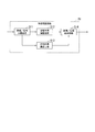
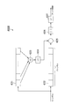
- FIG. 1 is a block diagram showing a configuration of a carrier phase synchronization circuit (CPR) and a phase cycle slip determination / compensation unit in an embodiment of the present invention.
- the symbol input to the CPR is branched to the carrier phase estimation unit 50 and the carrier phase compensation unit 60.
- the carrier phase estimation unit 50 the input symbols are input to the gain adjustment circuit 51.
- the gain adjustment circuit 51 calculates the amplitude value and the phase value of the input symbol, and the amplitude / phase separation circuit 511 for separation and the amplitude value separated by the amplitude / phase separation circuit 511 are
- the input amplitude gain adjustment circuit 512, the phase gain adjustment circuit 513 to which the phase value separated by the amplitude / phase separation circuit 511 is inputted, the output of the amplitude gain adjustment circuit 512 and the output of the phase gain adjustment circuit 513 are combined.
- the amplitude / phase coupling circuit 514 converts the complex number into a complex number.
- the operation is equivalent to an M-power circuit in CPR to which the Viterbi / Viterbi algorithm is applied.
- the amplitude gain adjustment circuit 512 holds the amplitude value
- the phase gain adjustment circuit 513 multiplies the phase, thereby improving the detection accuracy of the phase cycle slip determination / compensation unit 70 described later. Let That is, the operation of this embodiment is different from that of the M-th power circuit in CPR to which the Viterbi / Viterbi algorithm is applied.
- the setting value of the gain adjustment circuit 51 is not limited to the setting value described above.
- the gain setting values in the amplitude gain adjustment circuit 512 and the phase gain adjustment circuit 513 are the average window width of the averaging circuit 52, the tap length and band of the low-pass filter (LPF) 71 of the phase cycle slip determination / compensation circuit 70.
- the width is set based on the delay width of the delay difference section.
- the output of the gain adjustment circuit 51 is input to the averaging circuit 52.
- the averaging is performed by adding the symbols calculated by the gain adjustment circuit 51 and the averaging window width L including the symbols calculated before and after the symbol on the complex plane. Reduce ingredients.
- the output of the averaging circuit 52 is input to the angle calculation circuit 53.
- the angle calculation circuit 53 calculates the deflection angle of the symbol (complex number) averaged by the averaging circuit 52. If the noise is sufficiently reduced by the averaging circuit 52, the output of the angle calculation circuit 53 is M ⁇ k.
- the calculation method by the angle calculation circuit 53 is, for example, calculating the in-phase component (I) and the quadrature component (Q) of the output of the averaging circuit 52 and calculating arctan (Q / I), thereby converting the symbol into an angle. .
- the unwrap circuit corrects the arbitraryness (360 ° ⁇ n, where n is an integer) remaining in the angle calculated by the angle calculation circuit 53. Specifically, the unwrap circuit corrects the angle so that the difference between the angle with respect to the previous input symbol and the current angle becomes small.
- the division circuit 54 calculates the carrier phase estimation value by multiplying the angle corrected in the unwrap circuit by (1 / M).
- the complex number calculation circuit 55 calculates a complex number of size 1 with the carrier phase estimation value calculated by the division circuit 54 as an argument, and outputs the complex number to the multiplication circuit 62.
- the delay circuit 61 gives a delay corresponding to the time required for the calculation from the gain adjustment circuit 51 to the complex number calculation circuit 55 to the input symbol, and multiplies the input symbol at the same timing as the complex number of size 1 corresponding to the input symbol.
- the multiplier circuit 62 multiplies the input symbol delayed by the delay circuit 61 and the complex number calculated by the complex number calculation circuit 55, and synchronizes with the carrier phase of the input symbol.
- the estimated error phase calculated by the division circuit 54 is input to the delay difference circuit 72 via the LPF 71.
- the delay difference circuit 72 calculates the time variation of the estimated error phase.
- the slip determination unit 73 determines whether or not a phase cycle slip has occurred with respect to the input signal based on the temporal variation of the estimated error phase calculated by the delay difference unit 72. There are three types of determination of the phase cycle slip, 90 degrees, -90 degrees, and 180 degrees, and these can be determined by the polarity and absolute value of the time variation.
- the slip compensation unit 75 compensates the phase cycle slip for the input signal in which the phase error is reduced by the carrier phase compensation unit 60.
- the phase cycle slip compensation 90 ° subtraction is performed on the phase estimation value after the occurrence of the phase cycle slip when the 90 ° slip is determined.
- 90 degree is added to the phase estimation value.
- 180 degree slip determination 180 degree addition (or subtraction) is performed on the phase estimation value.
- the slip compensation unit 75 outputs a signal obtained by compensating the phase cycle slip for the input signal as an output signal. Further, when the slip determination unit 73 determines that the phase cycle slip has not occurred, the slip compensation unit 75 outputs the input signal whose phase error has been reduced by the carrier phase compensation unit 60 as an output signal.
- FIG. 3 shows the effect of this embodiment.
- FIG. 3 shows the effect of reducing the phase cycle slip ratio when the present invention is applied to the conventional configuration of CPR.
- the gain adjustment circuit 51 is provided, so that the estimation accuracy of the carrier phase estimation value in the carrier phase estimation unit 50 is improved, so the slip ratio is lowered.
- the gain adjustment circuit is not provided and the phase cycle slip determination / compensation unit 70 is provided, the slip ratio is reduced by compensating the generated phase cycle slip.
- the gain adjustment circuit 51 and the phase cycle slip determination / compensation unit 70 are provided, so that the estimation accuracy of the carrier phase estimation unit 50 is improved, and further, the phase cycle slip determination unit 73 detects the phase cycle slip. Since detection accuracy can be improved, the slip ratio can be reduced to about 1/100 of the conventional configuration.
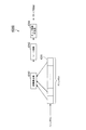
- FIG. 4 is a block diagram illustrating a configuration example of a receiving device according to the second embodiment.
- the receiving apparatus 80 shown in the figure is an application of the present invention in a digital coherent transmission system.
- An optical signal transmitted through the optical fiber transmission line is input to the receiving device 80.
- the receiving device 80 acquires data included in the input optical signal and outputs the acquired data to a device or the like connected to the subsequent stage.
- the receiver 80 includes a local laser generator 81, an optical 90-degree hybrid 82, a photoelectric conversion unit 83, an AD converter 84, a chromatic dispersion compensation unit 85, an adaptive equalization unit 86, a frequency offset compensation unit 87, and a phase cycle slip reduction unit. 88, a phase compensation unit 89, an error correction / determination unit 90, and a client interface 91.
- the optical signal input to the receiving device 80 is input to the optical 90-degree hybrid 82, mixed by the local oscillation laser output from the local laser generator 81 and the optical 90-degree hybrid 82, and subjected to homodyne detection or heterodyne detection.
- the optical signal obtained by the detection is converted into a baseband analog electric signal in the photoelectric conversion unit 83.
- This analog electrical signal is digitized by the AD converter 84 and output to the chromatic dispersion compensator 85.
- the digital signal output from the AD converter 84 is a signal indicating a symbol represented by a complex number having an in-phase component I and a quadrature component Q.
- the chromatic dispersion compensation unit 85 compensates the waveform distortion caused by the chromatic dispersion for the symbol input from the AD converter 84.
- the adaptive equalization unit 86 compensates for distortions caused by linear polarization crosstalk, polarization mode dispersion, and the like for the symbols whose waveform distortion has been compensated for by the chromatic dispersion compensation unit 85.
- the frequency offset compensation unit 87 compensates for the influence of the frequency offset that may occur between the transmission device that transmits the optical signal and the reception device 80 on the symbol whose distortion has been compensated by the adaptive equalization unit 86.
- the frequency offset is caused by, for example, a frequency shift between local oscillation lasers used in the transmission device and the reception device.
- the phase cycle slip reduction unit 88 and the phase compensation unit 89 perform phase compensation on the symbols for which the frequency offset has been compensated by the frequency offset compensation unit 87 to reduce the occurrence of phase cycle slip.
- the error correction / determination unit 90 demodulates the symbol whose phase has been compensated by the phase compensation unit 89, performs error detection and error correction on the data obtained by the demodulation, and then inputs the data to the client interface 91.
- the client interface 91 converts and outputs the data input from the error correction / determination unit 90 according to the signal format and frame configuration used in the apparatus connected to the subsequent stage of the receiving apparatus.
- the digital signal processing unit 92 including the chromatic dispersion compensation unit 85 to the client interface 91 converts the received optical signal into an electric signal using coherent detection, and receives the electric signal converted into a digital signal. A signal is input.
- the received signal input to the digital signal processing unit 92 is a signal indicating a symbol string in which data is mapped based on a modulation method used in the transmission apparatus.
- waveform distortion and noise added by the optical fiber transmission line, the transmitting device, and the receiving device are reduced or compensated by the chromatic dispersion compensation unit 85 and the adaptive equalization unit 86.
- the phase compensator 89 in this embodiment is intended to estimate and remove or reduce the phase noise superimposed on the carrier wave.
- the phase cycle slip reduction unit 88 and the phase compensation unit 89 will be described in detail.
- the phase compensation unit 89 performs carrier phase estimation from the received symbol sequence. If a so-called outlier is included in the symbols of the received symbol sequence used for carrier phase estimation, accurate carrier phase estimation cannot be performed and phase cycle slip occurs.
- the phase compensation unit 89 has a function of detecting a so-called outlier by performing statistical processing on each symbol of the received symbol sequence, and performing carrier phase estimation after reducing the influence of the outlier symbol.
- the phase cycle slip reduction unit 88 detects the occurrence of the phase cycle slip by using the output of the frequency offset compensation unit 87, and the received symbol that has been erroneously phase compensated by the phase cycle slip is erroneously detected by the phase cycle slip. Minute phase compensation.
- FIG. 5 is a block diagram showing a configuration of a phase compensation circuit according to the third embodiment.
- the phase cycle slip reduction unit / carrier phase estimation unit 501 and the carrier phase compensation unit 60 correspond to the phase cycle slip reduction unit 88 shown in FIG. This corresponds to the phase compensator 89 shown in FIG.
- the input symbols sequentially input to the phase compensation circuit are input to a gain adjustment circuit 51 (hereinafter referred to as an Nth power circuit) that functions as an Nth power circuit and a delay circuit 61.
- an N-th power circuit is described as an example of the gain adjustment circuit 51, and the present invention is not limited to this.
- the Nth power circuit 51 raises the input symbol to the Nth power.
- N-th power calculation for input symbols eliminates data dependency of 2 bits (1, 1), (1, -1) (-1, 1) and (-1, -1) redundant for each symbol It is to do.
- the tap coefficient calculation circuit 56 detects an outlier by performing statistical processing on the N-th input symbol.
- the tap coefficient calculation circuit 56 calculates and outputs a tap coefficient corresponding to the symbol as an outlier in order to reduce the influence of the outlier.
- the averaging circuit 52 multiplies the N-th power value of the input symbol calculated by the N-th power circuit by the N-th power value of the preceding and following input symbols by the multiplication circuit 57 and then the averaging window width M every Are added on the complex plane to average and reduce the noise component.
- the angle calculation circuit 53 calculates the deflection angle of the symbol (complex number) averaged by the averaging circuit 52.
- the symbol is converted into an angle by arctan (Q / I).
- the unwrap circuit included in the angle calculation circuit 53 corrects the arbitraryness (360 ° ⁇ n, where n is an integer) remaining in the angle calculated by the angle calculation circuit 53. Specifically, the unwrap circuit corrects the angle so that the difference between the angle with respect to the previous input symbol and the current angle becomes small.
- the division circuit 54 calculates the carrier phase estimation value by multiplying the angle corrected in the unwrapping circuit by (1 / N).
- the complex number calculation circuit 55 calculates a complex number having a magnitude of 1 with the carrier phase estimation value calculated by the division circuit 54 as an argument, and outputs the complex number to the multiplication circuit 62.
- the delay circuit 61 gives a delay corresponding to the time required for the calculation from the N-th power circuit 51 to the complex number calculation circuit 55 to the input symbol, and multiplies the input symbol at the same timing as the complex number of size 1 corresponding to the input symbol.
- the multiplier circuit 62 multiplies the input symbol delayed by the delay circuit 61 and the complex number calculated by the complex number calculation circuit 55 to compensate for phase noise and the like included in the input symbol.
- the estimated error phase calculated is input to the delay difference circuit 72 via the LPF 71.
- the delay difference circuit 72 calculates the time variation of the estimated error phase.
- the slip determination unit 73 determines whether or not a phase cycle slip has occurred with respect to the input signal based on the temporal variation of the estimated error phase calculated by the delay difference unit 72. There are three types of determination of the phase cycle slip, 90 degrees, -90 degrees, and 180 degrees, and these can be determined by the polarity and absolute value of the time variation.
- the slip compensation unit 75 compensates the phase cycle slip for the input signal whose phase error has been reduced by the carrier phase compensation unit 60. .
- 90 ° subtraction is performed on the phase estimation value after the occurrence of the phase cycle slip when the 90 ° slip is determined.
- 90 degree is added to the phase estimation value.
- 180 degree addition is performed on the phase estimation value.
- the slip compensation unit 75 outputs a signal obtained by compensating the phase cycle slip for the input signal as an output signal. Further, when the slip determination unit 73 determines that the phase cycle slip has not occurred, the slip compensation unit 75 outputs the input signal whose phase error has been reduced by the carrier phase compensation unit 60 as an output signal.
- FIG. 6 is a block diagram showing a configuration of a phase compensation circuit according to the fourth embodiment of the present invention.
- the phase compensation circuit is used for an optical receiver in an optical communication system.
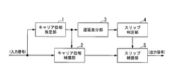
- the phase compensation circuit includes a carrier phase estimation unit 1, a carrier phase compensation unit 2, a delay difference unit 3, a slip determination unit 4, and a slip compensation unit 5.
- a digital signal obtained by performing an analog-digital conversion after photoelectrically converting the received optical signal is input as an input signal.
- the input signal is subjected to compensation for chromatic dispersion, compensation for distortion during transmission, and the like as necessary before being input to the phase compensation circuit.
- the carrier phase estimation unit 1 performs carrier phase estimation on an input signal by a feedback method or a feedforward method.
- the carrier phase estimation unit 1 outputs an estimation error phase that is an estimation value of the carrier phase error to the carrier phase compensation unit 2 and the delay difference unit 3.
- the carrier phase compensation unit 2 reduces the phase error included in the input signal based on the estimated error phase.
- the delay difference unit 3 calculates the time variation of the estimated error phase.
- the slip determination unit 4 determines whether or not a phase cycle slip has occurred with respect to the input signal based on the temporal variation of the estimated error phase calculated by the delay difference unit 3.
- the slip compensation unit 5 When the slip determination unit 4 determines that a phase cycle slip has occurred, the slip compensation unit 5 performs phase cycle slip compensation on the input signal whose phase error has been reduced by the carrier phase compensation unit 2. The slip compensation unit 5 outputs a signal obtained by compensating the phase cycle slip for the input signal as an output signal. Further, when it is determined by the slip determination unit 4 that no phase cycle slip has occurred, the slip compensation unit 5 outputs an input signal whose phase error has been reduced by the carrier phase compensation unit 2 as an output signal.
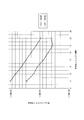
- FIG. 7 is a graph showing an example of the estimation error phase output from the carrier phase estimation unit 1. That is, FIG. 7 is a graph showing the phase compensation amount of the past 1280 symbols (corresponding to the protection stage) at the time of detecting the phase slip.
- the horizontal axis indicates the symbol number in the input signal
- the vertical axis indicates the phase compensation amount.
- the phase compensation amount is a phase amount when the phase error is reduced based on the estimated error phase.
- a steep fluctuation of the estimation error phase occurs in the area indicated by the broken line, that is, in the vicinity of the symbol number 800. This steep fluctuation is due to the occurrence of a phase cycle slip.
- the carrier phase estimation unit 1 When the fluctuation of the estimation error phase is seen, as shown in FIG. 7, when the phase cycle slip occurs, the carrier phase estimation unit 1 has a short period of several times the average of the filter tap length (average of tap lengths). Change of about ( ⁇ / 2) radians to about 100 symbols). On the other hand, when the phase cycle slip does not occur, the estimated error phase does not change so as to exceed 1 radian in a short time.
- phase cycle slip detection and phase cycle slip compensation are performed. Specifically, the estimation error phase output by the carrier phase estimation unit 1 is monitored, and it is determined that a phase cycle slip has occurred when a steep fluctuation is detected in a short time, and the phase cycle slip is compensated for the input signal. Do.
- the steep variation is, for example, a variation exceeding 1 radian.
- phase cycle slip occurrence frequency (1 ⁇ (detection rate)) + (number of false detections)
- the detection rate is a ratio at which the phase cycle slip can be detected by the slip determination unit 4, and the number of erroneous detections is the number of times that the slip cycle determination unit 4 erroneously determines that the phase cycle slip has occurred.
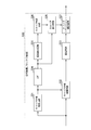
- FIG. 8 is a block diagram illustrating a configuration example of an optical communication system according to the fifth embodiment of the present invention.
- the optical communication system according to the present embodiment includes an optical signal transmitter 11, a transmission path 12 including a single mode optical fiber transmission path and an optical amplifier, and an optical signal receiver 13.
- the optical signal transmission device 11 outputs an optical signal obtained by polarization-multiplexing a signal obtained using a QPSK modulation format to the optical signal reception device 13 via the transmission line 12.
- operation coding is not performed.
- a configuration for transmitting and receiving a polarization-multiplexed signal using the QPSK scheme as a modulation format will be described.
- an m-QAM modulation format such as BPSK (Binary Phase Shift Keying) or 16QAM (Quadrature Amplitude Modulation) may be used, or a single polarization signal may be transmitted and received.
- BPSK Binary Phase Shift Keying
- 16QAM Quadrature Amplitude Modulation
- FIG. 9 is a block diagram illustrating a configuration example of the optical signal receiving device 13 in the present embodiment.
- the optical signal receiver 13 acquires data converted into an optical signal in the optical signal transmitter 11 from the optical signal input via the transmission path 12.
- the optical signal receiving device 13 includes a local laser generator 14, a 90 ° optical hybrid 15, a photoelectric converter 16, an analog-digital converter (AD converter) 17, and a digital signal processing unit 18.
- the optical signal input to the optical signal receiving device 13 is mixed by the local oscillation laser output from the local laser generator 14 and the 90 ° optical hybrid 15 and subjected to homodyne detection or heterodyne detection.
- the optical signal obtained by the detection is converted into a 4-lane baseband analog electrical signal by the photoelectric converter 16.
- the analog electric signal is digitized by the analog-digital converter 17 and output to the digital signal processing unit 18 as a two-lane complex digital signal of X polarization and Y polarization.
- the digital signal processing unit 18 demodulates and decodes the complex digital signal of X polarization and Y polarization after compensating for linear waveform distortion.
- the digital signal processing unit 18 outputs the data obtained by demodulation and decoding to a device connected to the subsequent stage.
- the digital signal processing unit 18 includes a chromatic dispersion compensation circuit 19, an adaptive equalization circuit 20, a frequency offset compensation circuit 21, a phase compensation circuit 22, a demodulation / decoding circuit 23, and a client interface 24.
- the complex digital signal (received signal) of X polarization and Y polarization input to the digital signal processing unit 18 is linearly mixed due to the influence of rotation of the polarization state in the transmission path 12 or the like.
- the chromatic dispersion compensation circuit 19 compensates for the linear waveform distortion due to chromatic dispersion for the complex digital signal of X polarization and Y polarization input to the digital signal processing unit 18.
- the adaptive equalization circuit 20 performs linear polarization crosstalk, polarization mode dispersion (PMD), etc. on the complex digital signal of the X polarization and Y polarization whose wavelength dispersion has been compensated in the wavelength dispersion compensation circuit 19. Compensates for distorted signals in the transmission path.
- the frequency offset compensation circuit 21 can be generated between the optical signal receiving apparatus and the optical signal transmitting apparatus with respect to the complex digital signal of X polarization and Y polarization whose distortion has been compensated for in the adaptive equalization circuit 20. Compensate for the effects of frequency offset.
- the frequency offset is caused by, for example, a frequency shift between locally transmitted lasers used in the optical signal transmitter 11 and the optical signal receiver 13.
- the phase compensation circuit 22 compensates the phase cycle slip for the complex digital signal of the X polarization and the Y polarization whose frequency offset has been compensated for in the frequency offset compensation circuit 21.
- the demodulation / decoding circuit 23 performs demodulation corresponding to the modulation format used in the optical signal transmitting apparatus 11 on the complex digital signal of X polarization and Y polarization whose phase cycle slip has been compensated in the phase compensation circuit 22. Perform error correction decoding.
- the demodulation / decoding circuit 23 outputs data obtained by demodulation and error correction decoding to the client interface 24.
- the client interface 24 converts and outputs the data input from the demodulation / decoding circuit 23 according to the signal format and frame configuration used in the apparatus connected to the subsequent stage of the digital signal processing unit 18.
- FIG. 10 is a block diagram showing a configuration example of the phase compensation circuit 22 in the present embodiment.
- the phase compensation circuit 22 includes a phase compensation block 220 corresponding to X polarization and a phase compensation block 220 corresponding to Y polarization.
- the phase compensation block 220 corresponding to the X polarization is described, and the description of the phase compensation block 220 corresponding to the Y polarization having the same configuration is omitted.
- the phase compensation block 220 includes a carrier phase estimation circuit 221, a carrier phase compensation circuit 222, a delay circuit 223, a low-pass filter (LPF) 224, a delay difference circuit 225, a slip determination circuit 226, and a slip compensation circuit 227. .
- An X-polarized complex digital signal is input to the phase compensation block 220.
- the carrier phase estimation circuit 221 estimates, for example, a carrier phase error of a feed forward method as described in Non-Patent Document 1 or a feedback method as described in Reference Document 1 (Reference Document 1: T.Kobayashi et al, "160-Gb / s Polarization-Multiplexed 16-QAM long-haul transmission over 3,123 km using digital coherent receiver with digital PLL based frequency offset compensator", OTuD1 OFC / NFOEC2010).
- the carrier phase estimation circuit 221 estimates the phase difference between the optical signal transmission device 11 and the optical signal reception device 13 due to a locally transmitted laser or the like. Since this phase difference fluctuates with time, the carrier phase estimation circuit 221 continuously performs carrier phase estimation and performs estimation following the fluctuation of the phase difference. For example, when the modulation format is QPSK, feedforward type carrier phase estimation based on the fourth power method is performed. Further, carrier phase estimation is performed based on the square method in the case of the BPSK method, and based on the maximum likelihood determination (ML) method in the case of the m-QAM method. That is, the carrier phase estimation circuit 221 uses a phase estimation method appropriate for the modulation format.
- the modulation format is QPSK
- feedforward type carrier phase estimation based on the fourth power method is performed.
- carrier phase estimation is performed based on the square method in the case of the BPSK method, and based on the maximum likelihood determination (ML) method in the case of the m-QAM method. That is, the carrier phase estimation circuit 2
- the carrier phase estimation circuit 221 estimates a phase error included in the X-polarized complex digital signal.
- the carrier phase estimation circuit 221 outputs an estimation error phase that is an estimated phase error to the carrier phase estimation circuit 221 and the low-pass filter 224.
- the carrier phase compensation circuit 222 compensates for the phase error included in the X-polarized complex digital signal based on the estimated error phase output from the carrier phase estimation circuit 221.
- the carrier phase compensation circuit 222 outputs an X-polarized complex digital signal whose phase error is compensated to the delay circuit 223.
- the phase error is a phase that does not depend on the modulation component in the phase of the complex digital signal. For example, it occurs due to the phase difference of the locally transmitted laser between the optical signal transmitter 11 and the optical signal receiver 13, the nonlinearity of the transmission path, or the like.
- FIG. 11 is a block diagram showing a configuration example of the carrier phase estimation circuit 221.
- the carrier phase estimation circuit 221 shown in the figure has a feed forward configuration.
- the carrier phase estimation circuit 221 includes a phase m multiplication circuit 2211, a K symbol averaging circuit 2212, a phase extraction circuit 2213, and a phase continuation circuit 2214.
- the output of the phase m multiplication circuit 2211 is input to the K symbol averaging circuit 2212.
- FIG. 12 is a block diagram illustrating a configuration example of the phase m multiplication circuit 2211 in the present embodiment.
- the phase m multiplication circuit 2211 includes an amplitude / phase separation circuit 22111, a multiplier 22112, and an amplitude / phase recombination circuit 22113.
- a signal input to the phase m multiplication circuit 2211 is separated into a phase component and an amplitude component by an amplitude / phase separation circuit 22111.
- the phase component separated in the amplitude / phase separation circuit 22111 is multiplied by m by the multiplier 22112.
- the phase component multiplied by m by the multiplier 22112 and the amplitude component separated by the amplitude / phase separation circuit 22111 are reconstructed into a complex signal by the amplitude / phase recombination circuit 22113 and output.
- FIG. 13 is a block diagram illustrating a configuration example of the K symbol averaging circuit 2212.
- the K symbol averaging circuit 2212 is configured as a finite impulse response filter having a tap length K.
- the output of the K symbol averaging circuit 2212 is input to the phase extraction circuit 2213.
- the phase extraction circuit 2213 extracts and outputs the phase component of the complex input signal.
- the output of the phase extraction circuit 2213 takes a value of 2 ⁇ , for example, from ⁇ to + ⁇ radians.
- the range that can be taken by the phase continuation circuit 2214 is ideally set to ⁇ infinity (actually, Enlarge to a large enough range to remove phase discontinuities.
- Various techniques have been proposed for the phase continuation algorithm for a long time.
- a signal from which the phase discontinuity is removed by the phase continuation circuit 2214 is output as an estimated error phase that is an output of the carrier phase estimation circuit 221.
- the delay circuit 223 gives a delay of the time (number of symbols) required for signal processing in the low-pass filter 224, the delay difference circuit 225, and the slip determination circuit 226 to the complex digital signal output from the carrier phase compensation circuit 222. Output to the slip compensation circuit 227. That is, the delay circuit 223 inputs the timing at which the complex digital signal output from the carrier phase compensation circuit 222 is input to the slip compensation circuit 227 and the determination result of the slip determination circuit 226 for the complex digital signal to the slip compensation circuit 227. A delay is given so that the timing is aligned.
- the delay circuit 223 can be configured using a shift register, for example. In this case, one shift delay amount is one symbol time.
- the low-pass filter 224 smoothes the fluctuation of the estimation error phase output from the carrier phase estimation circuit 221, removes the high frequency component in the estimation error phase, and outputs it to the delay difference circuit 225.
- the delay difference circuit 225 outputs a signal proportional to the time variation of the estimated error phase smoothed by the low-pass filter 224.
- the signal output from the delay difference circuit 225 is a signal indicating the delay difference value d.
- the delay difference value d is calculated using the following equation (3) by monitoring the estimated error phase ( ⁇ (nT)) that varies with time over N symbols.
- the delay difference circuit 225 outputs a signal indicating the calculated delay difference value d to the slip determination circuit 226.
- n is a natural number and a symbol number
- T is a symbol time interval.
- FIG. 14 is a block diagram showing a configuration example of the delay difference circuit 225 in the present embodiment.
- the delay difference circuit 225 includes an N symbol delay unit 2251, a multiplier 2252, and an adder 2253.
- the estimated error phase ( ⁇ (nT)) smoothed by the low-pass filter 224 is input to the N symbol delay unit 2251 and the adder 2253.
- N symbol delay unit 2251 outputs an estimated error phase ( ⁇ ((n ⁇ N) T)) N symbols before.
- the N symbol delay unit 2251 can be configured using a shift register, for example. In this case, one shift delay amount is one symbol time, and the range to be stored is about five times the filter tap length K in the K symbol averaging circuit 2212.
- Multiplier 2252 multiplies the estimated error phase N symbols before output from N symbol delay unit 2251 by ( ⁇ 1) and outputs adder 2253.
- the adder 2253 adds the estimated error phase output from the low pass filter 224 and the value output from the multiplier 2252. That is, the adder 2253 performs the calculation of Expression (3) and outputs the calculation result as the delay difference value d.
- N (the number of delay symbols) in the N symbol delay unit 2251 is set in advance in a range of about 1 to 5 times the average value of the number of taps of the filter in the K symbol averaging circuit 2212.
- N is set to a value such that a steep fluctuation in the estimation error phase as shown in FIG. 7 can be detected, and that erroneous detection due to fluctuation due to fluctuations in the estimation error phase is less likely to occur.
- the signal output from the delay difference circuit 225 having such a configuration indicates an amount proportional to the temporal slope of the estimated error phase (the amount of change in slope per unit time).
- the slip determination circuit 226 compares the delay difference value d output from the delay difference circuit 225 with a predetermined detection threshold value to determine whether or not a phase cycle slip has occurred, and if a phase cycle slip has occurred, Determine the direction. As shown in FIG. 7, when a steep fluctuation of the estimated phase error occurs, the absolute value of the delay difference value d increases. The determination as to whether or not a phase cycle slip has occurred is made based on whether or not d has continuously exceeded the threshold over about L symbols.
- L is a value corresponding to the delay value N of the delay difference circuit 225 described above, and is a value satisfying 0 ⁇ L ⁇ N.
- the slip determination circuit 226 outputs to the slip compensation circuit 227 a slip determination signal indicating the determination result of whether or not the phase cycle slip has occurred and the rotation direction when the phase cycle slip has occurred.
- the detection threshold for the delay difference value d differs depending on the modulation format. For example, when the QPSK method or the QAM method is used, a value of about 1 radian is used. However, in actuality, a detection threshold value that minimizes the occurrence frequency (residual slip frequency) of the phase cycle slip remaining in the complex digital signal output from the phase compensation block 220 is set in accordance with conditions such as the amount of phase noise. It is appropriate to do.
- the occurrence frequency of the phase cycle slip is calculated by, for example, (number of occurrences of phase cycle slip) / (number of transmission symbols).
- the detection threshold value for the delay difference value d is set based on, for example, a simulation or an actual measurement result. It should be noted that the range that the optimum value can take is from 0 radians to ( ⁇ /) for a modulation format in which the phase difference between symbols in the constellation is ( ⁇ / 2) radians, such as the QPSK method and the QAM method. 2) The range is up to radians. For the m-PSK modulation format, the range is from 0 radians to (2 ⁇ / m) radians.
- the frequency offset compensation circuit 21 cannot sufficiently compensate. It is desirable to change the detection threshold according to the residual frequency offset.
- the slip compensation circuit 227 receives the slip determination signal output from the slip determination circuit 226 and the complex digital signal output from the delay circuit 223.
- the slip compensation circuit 227 compensates for the phase of the complex digital signal based on the phase compensation amount switched according to the slip determination signal.
- the phase compensation amount in the slip compensation circuit 227 is one of 0 °, 90 °, 180 °, and 270 ° when the modulation format is the QPSK method or the QAM method.
- the phase compensation amount has an initial value of 0 °, for example, and is switched between positive rotation and negative rotation in units of 90 ° according to the slip determination signal.
- positive rotation is rotation in which the phase increases
- negative rotation rotation in which the phase decreases.
- the phase compensation amount for the complex digital signal is switched in units of (360 ° / m). Further, the phase compensation amount switched according to the slip determination signal is maintained until the next occurrence of the phase cycle slip is detected.
- the slip compensation circuit 227 always performs phase compensation on the complex digital signal output from the delay circuit 223 by the phase compensation amount switched by the slip determination signal.
- FIG. 15 is a flowchart showing a slip determination process performed by the slip determination circuit 226 in the present embodiment.
- the slip determination circuit 226 inputs the delay difference value d output from the delay difference circuit 225 (step S101).
- the slip determination circuit 226 determines whether or not the absolute value of the input delay difference value d is greater than a predetermined detection threshold Th (step S102).
- step S102 If the absolute value is not larger than the detection threshold Th (step S102: NO), the slip determination circuit 226 initializes the parameter p and q by substituting 0 for the parameters p and q (step S103), and returns the process to step S101.
- the parameter p is a parameter for counting the number of symbols for which the delay difference value d continuously exceeds the detection threshold Th in the forward rotation direction.
- the parameter q is a parameter for counting the number of symbols for which the delay difference value d continuously exceeds the detection threshold Th in the negative rotation direction.
- step S104 determines whether or not the delay difference value d is larger than 0 (step S104).
- the slip determination circuit 226 increases the parameter q by 1 (step S105), and determines whether the parameter q exceeds the determination threshold L (step S105).
- the determination threshold L is a predetermined value corresponding to the delay value N of the delay difference circuit 225 as described above, and is, for example, a value about 60% of N (N ⁇ 0.6).
- the determination threshold L may be determined according to the degree of variation of the delay difference value d, the time interval between symbols, and the like, and a false detection of the phase cycle slip is a predetermined value based on a simulation or an actual measurement value. You may make it determine so that it may become the following.
- step S106: NO When the value of the parameter q does not exceed the determination threshold L (step S106: NO), the slip determination circuit 226 returns the process to step S101.
- step S106: YES When the value of the parameter q exceeds the determination threshold L (step S106: YES), the slip determination circuit 226 determines that a phase cycle slip in the negative rotation direction has occurred, and a phase cycle slip in the negative rotation direction has occurred. A slip determination signal indicating this is output to the slip compensation circuit 227 (step S107), and the process returns to step S101.
- step S104 When the delay difference value d is larger than 0 in step S104 (step S104: YES), the slip determination circuit 226 increases the parameter p by 1 (step S108), and determines whether the parameter p exceeds the determination threshold L. (Step S109).
- step S109: NO When the value of the parameter p does not exceed the determination threshold L (step S109: NO), the slip determination circuit 226 returns the process to step S101.
- step S109: YES When the value of the parameter p exceeds the determination threshold L (step S109: YES), the slip determination circuit 226 determines that a phase cycle slip in the forward rotation direction has occurred, and a phase cycle slip in the forward rotation direction has occurred. A slip determination signal indicating this is output to the slip compensation circuit 227 (step S110), and the process returns to step S101.
- the slip determination circuit 226 determines that a phase cycle slip has occurred when the absolute value of the delay difference value d exceeds the detection threshold Th continuously over L symbols, that is, when the difference delay value d changes significantly. judge. At this time, the slip determination circuit 226 determines that a positive rotation phase cycle slip has occurred when the delay difference value d exceeds a detection threshold Th (Th> 0; upper detection threshold) that takes a positive value. Further, the slip determination circuit 226 determines that a negative rotation phase cycle slip has occurred when the delay difference value d is below the detection threshold ( ⁇ Th) (lower detection threshold) that takes a negative value.
- the slip compensation circuit 227 switches the phase compensation amount based on the slip determination signal indicating the determination result by the slip determination circuit 226 and performs compensation for the complex digital signal output from the delay circuit 223.
- This time lag is a processing time in the low-pass filter 224, the delay difference circuit 225, the slip determination circuit 226, and the slip compensation circuit 227.
- the delay circuit 223 compensates for this time lag.
- the slip compensation circuit 227 performs phase cycle slip compensation on the complex digital signal output from the carrier phase compensation circuit 222 by the phase compensation amount according to the slip determination signal.
- the phase compensation circuit 22 monitors the output of the carrier phase estimation circuit 221 to immediately detect and correct the generated phase cycle slip without using a redundant signal such as a pilot symbol. it can. Thereby, the substantial occurrence frequency of the phase cycle slip can be suppressed, and the coherent optical communication using the absolute phase can be performed while suppressing the redundancy of the signal by the pilot symbol or the like.
- the redundancy is calculated by, for example, (number of pilot symbols per unit time) / (number of so-friendly symbols per unit time).
- phase compensation circuit 22 by providing a low pass filter 224 between the carrier phase estimation circuit 221 and the delay difference circuit 225, fluctuations due to fluctuations in the estimation error phase and noise are smoothed. Thereby, the detection accuracy of the phase cycle slip using the delay difference value d can be improved.
- FIG. 16 is a schematic block diagram showing a configuration of an experimental apparatus used for acquiring optical transmission experimental data.
- a block described as “offline DSP” corresponds to the digital signal processing unit 18.
- FIG. 17 is a graph showing the results of offline demodulation of optical transmission experiment data obtained by the experimental apparatus shown in FIG.
- the horizontal axis indicates the tap length in the carrier phase estimation circuit 221 and the K symbol averaging circuit 2212
- the vertical axis indicates the bit error rate (BER) and the symbol slip rate (SlipRate).
- BER bit error rate
- SlipRate symbol slip rate
- the effect of burst error due to phase cycle slip can be suppressed below the allowable threshold for forward error correction using pilot symbols with a redundancy of about 1%. It is possible to avoid it.
- the condition of the optical signal-to-noise ratio necessary for obtaining a bit error rate of 1 ⁇ 10 ⁇ 2 can be relaxed by about 1.1 to 1.4 dB by avoiding differential coding.
- FIG. 18 is a block diagram showing the configuration of the phase compensation block 320 in the sixth embodiment. Although the phase compensation block 320 corresponding to the X polarization is shown here, the same phase compensation block 320 is used for the Y polarization.
- the phase compensation block 320 in this embodiment includes a carrier phase estimation circuit 221, a carrier phase compensation circuit 222, a delay circuit 223, a low-pass filter 224, a delay difference circuit 225, a slip determination circuit 326, a slip compensation circuit 227, and a threshold value calculation circuit. 328.
- the phase compensation block 320 includes a slip determination circuit 326 instead of the slip determination circuit 226 and a threshold value calculation circuit 328 according to the fifth embodiment (FIG. 10). ) Is different. Note that in the phase compensation block 320, the same reference numerals are given to the same components as those in the fifth embodiment, and description thereof is omitted.
- the slip determination circuit 326 receives the delay difference value d output from the delay difference circuit 225 and the detection threshold value including the upper detection threshold value and the lower detection threshold value calculated by the threshold value calculation circuit 328. The slip determination circuit 326 determines that a forward rotation phase cycle slip has occurred when the delay difference value d exceeds the upper detection threshold continuously over L symbols. The slip determination circuit 326 determines that a negative rotation phase cycle slip has occurred when the delay difference value d continuously falls below the lower detection threshold for L symbols. The slip determination circuit 326 outputs to the slip compensation circuit 227 a slip determination signal indicating the determination result of whether or not the phase cycle slip has occurred and the rotation direction when the phase cycle slip has occurred.
- the threshold calculation circuit 328 receives the delay difference value d output from the delay difference circuit 225 and calculates a detection threshold according to the delay difference value d.
- FIG. 19 is a block diagram illustrating a configuration example of the threshold value calculation circuit 328 in the present embodiment.
- the threshold calculation circuit 328 includes a multiplier 3281, an adder 3282, a multiplier 3283, a delay unit 3284, an adder 3285, and a subtractor 3286.
- the delay difference value d is input to the multiplier 3281.
- Multiplier 3281 multiplies input delay difference value d by a predetermined coefficient ⁇ , and outputs the multiplication result to adder 3282.
- the adder 3282 receives the multiplication result from the multiplier 3281 and the value output from the delay unit 3284. Adder 3282 adds the value output from delay unit 3284 and the multiplication result, and outputs the addition result to multiplier 3283, adder 3285, and subtractor 3286.
- Multiplier 3283 multiplies the addition result output from adder 3282 by the coefficient (1- ⁇ ), and outputs the multiplication result to delay unit 3284.
- Delay device 3284 delays the multiplication result output from multiplier 3283 by one symbol and then outputs the result to adder 3282. That is, in the threshold calculation circuit 328, the exponent moving average D of the delay difference value d is calculated by the multiplier 3281, the adder 3282, the multiplier 3283, and the delayer 3284 as shown in the following equation (4).
- n is a symbol number.
- ⁇ is a forgetting factor.
- D (n + 1) (1- ⁇ ) D (n) + ⁇ d (n) (4)
- the adder 3285 adds the addition result (exponential moving average D) output from the adder 3282 and a predetermined threshold width, and outputs the addition result as an upper detection threshold.
- the subtractor 3286 subtracts the threshold width from the addition result (exponential moving average D) output from the adder 3282, and outputs the subtraction result as the lower detection threshold.
- the threshold width is, for example, about 1 radian. As the threshold width, a value corresponding to the modulation format is determined in the same manner as the detection threshold Th in the fifth embodiment.
- the threshold calculation circuit 328 adaptively calculates the detection threshold including the upper detection threshold and the lower detection threshold based on the delay difference value d, so that the complex digital signal input to the phase compensation block 320 is converted into a complex digital signal. Even when the frequency offset remains, the phase cycle slip can be detected and compensated with high accuracy.
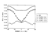
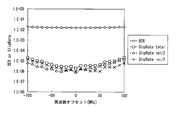
- 20A and 20B are graphs comparing the case where the detection threshold is set to a fixed value and the case where the detection threshold is determined according to the delay difference value d.
- the figure shows an example of the bit error rate (BER) and the symbol slip rate (SlipRate) when the detection threshold is a fixed value and when the detection threshold is determined according to the delay difference value d.
- the horizontal axis indicates the frequency offset
- the vertical axis indicates the bit error rate (BER) and the symbol slip rate (SlipRate).
- the tap length K in the K symbol averaging circuit 2212 is set to 17
- the delay amount in the delay difference circuit 225 is set to 60 symbols
- the optical signal to noise ratio (OSNR) is set to 12.5 dB.
- Other conditions are the same as those in the experimental apparatus shown in FIG.
- FIG. 20A shows the relationship between the bit error rate and symbol slip rate and the frequency offset when the detection threshold is fixed to 1 radian.
- the symbol slip rate indicates the positive rotation direction, the negative rotation direction, and the total of them.
- bit error rate / symbol slip ratio is good properties of 10 3.
- the frequency offset is around 50 MHz, the symbol slip rate has deteriorated by two orders of magnitude or more.
- FIG. 20B shows the relationship between the bit error rate and symbol slip rate and the frequency offset when the detection threshold is determined according to the delay difference value d.
- the threshold width is 1 radian and the forgetting factor ⁇ is 1 ⁇ 10 ⁇ 3 .
- the slip determination circuit 226 in the fifth embodiment is configured to determine whether or not a phase cycle slip has occurred based on the delay difference value d input from one delay difference circuit 225.
- a plurality of delay difference circuits 225 having different delay numbers (N symbols) are provided, and it is determined whether or not a phase cycle slip has occurred for each delay difference value d output from each delay difference circuit 225. To do. By making a majority decision based on the respective determination results, the accuracy of detecting the phase cycle slip is improved.
- FIG. 21 is a block diagram showing a configuration of the phase compensation block 420 according to the seventh embodiment. Although the phase compensation block 420 corresponding to the X polarization is shown here, the same phase compensation block 420 is used for the Y polarization.
- the phase compensation block 420 includes a carrier phase estimation circuit 221, a carrier phase compensation circuit 222, a delay circuit 223, a low-pass filter 224, three delay difference circuits 225-1 to 225-3, a slip determination circuit 426, and a slip compensation circuit 227. have.
- the phase compensation block 420 includes a plurality of delay difference circuits 225 and includes a slip determination circuit 426 instead of the slip determination circuit 226 in the fifth embodiment. It is different from FIG. Note that in the phase compensation block 420, the same components as those in the fifth embodiment are denoted by the same reference numerals, and description thereof is omitted.
- the delay difference circuits 225-1 to 225-3 have the same configuration as the delay difference circuit 225 in the fifth embodiment, but the delay amount by the N symbol delay unit 2251 is different.
- the slip determination circuit 426 performs a slip determination process (FIG. 15) for each delay difference value d output from each of the delay difference circuits 225-1 to 225-3.
- the slip determination circuit 426 determines whether or not a phase cycle slip has occurred and determines that a phase cycle slip has occurred by performing a majority decision using the determination result made for each delay difference value d.
- the rotation direction in the case is determined. Specifically, when at least two of the determination results in the slip determination process determine that a phase cycle slip in the same rotational direction has occurred, a slip determination signal indicating that a phase cycle slip has occurred is sent to the slip compensation circuit 227. Output.
- the phase compensation block 420 includes the three delay difference circuits 225 has been described.
- the configuration may include two delay difference circuits 225 or four or more delay difference circuits 225.
- the phase compensation amount is a predetermined discrete value.
- the phase compensation amount in the phase cycle slip compensation performed on the complex digital signal when the phase cycle slip is detected is set to a value corresponding to the estimated error phase.
- FIG. 22 is a block diagram showing the configuration of the phase compensation block 520 in the eighth embodiment. Although the phase compensation block 520 corresponding to the X polarization is shown here, the same phase compensation block 520 is used for the Y polarization.
- the phase compensation block 520 includes a carrier phase estimation circuit 221, a carrier phase compensation circuit 222, a delay circuit 223, a low-pass filter 224, a delay difference circuit 225, a slip determination circuit 226, a slip transient compensation circuit 527, and a slope calculation circuit 528. is doing.
- the phase compensation block 520 includes a slip transient compensation circuit 527 instead of the slip compensation circuit 227 and a slope calculation circuit 528.
- the phase compensation block 220 according to the fifth embodiment (FIG. It is different from 10). Note that in the phase compensation block 520, the same components as those in the fifth embodiment are denoted by the same reference numerals, and description thereof is omitted.
- the slip transient compensation circuit 527 updates the phase compensation amount for the complex digital signal output from the delay circuit 223 based on the compensation amount difference input from the slope calculation circuit 528.
- the phase compensation amount has an initial value of 0 °, for example, and is updated based on the compensation amount difference.
- the slope calculation circuit 528 receives the estimated error phase output from the low pass filter 224 and the slip determination signal output from the slip determination circuit 226. When it is determined that a phase cycle slip has occurred, the slope calculation circuit 528 calculates a compensation amount difference in the rotation direction indicated by the slip determination signal, and outputs the calculated compensation amount difference to the slip transient compensation circuit 527. The slope calculation circuit 528 calculates a compensation amount difference based on the estimated error phase.
- the slope calculation circuit 528 sets a value obtained by multiplying the estimated error phase by a predetermined coefficient as the compensation amount difference.
- This predetermined coefficient may be 1.
- the range that the compensation amount difference can take is a range according to the modulation format. For example, when the modulation format is QPSK or QAM, the range is 0 to ⁇ / 2 for the phase cycle slip in the positive rotation direction, and ⁇ for the phase cycle slip in the negative rotation direction. The range is from / 2 to 0.
- the amount of phase change in the complex digital signal that occurs when the phase compensation is performed can be reduced. Can do. Thereby, it is possible to improve the accuracy of detection and compensation of the phase cycle slip while suppressing the influence on the signal processing in the subsequent stage of the phase compensation circuit 22.
- the delay amount in the delay circuit 223 may be a value larger than the time (number of symbols) required for processing from the low-pass filter 224 to the slope calculation circuit 528.
- the configuration in which the carrier phase is estimated and compensated blindly using only data symbols has been described, but time-multiplexed pilot symbols may be used together. Thereby, the estimation accuracy of the carrier phase can be increased.
- the configuration in which the low-pass filter 224 smoothes the delay difference value d has been described.
- the delay difference circuit 225 may use an average value of differences between a plurality of past estimated phase errors and the current estimated phase error as the delay difference value d.
- the delay difference value d is calculated from a plurality of past estimated phase errors including an estimated phase error before N symbols and estimated phase errors before and after that. Thereby, the same processing as that of the low-pass filter 224 can be performed.
- phase compensation block having the same configuration for the X polarization and the Y polarization has been described.
- the phase compensation blocks having different configurations among the phase compensation blocks in the embodiments may be used in combination.
- the seventh embodiment or the eighth embodiment may be configured to include the threshold value calculation circuit 328 shown in the sixth embodiment.
- the threshold calculation circuit 328 is applied to the seventh embodiment, the threshold calculation circuit 328 is provided for each of the plurality of delay difference circuits 225.
- a plurality of delay difference circuits 225 may be provided.
- the program for realizing the functions of the digital signal processing unit 18 in each of the fourth to eighth embodiments can be realized by being mounted on a custom LSI (ASIC) or FPGA.
- the program may be recorded on a computer-readable recording medium, and the program recorded on the recording medium may be read into a computer system and executed to obtain data from the complex digital signal.
- the “computer system” includes an OS and hardware such as peripheral devices.
- the “computer system” includes a WWW system having a homepage providing environment (or display environment).
- the “computer-readable recording medium” refers to a storage device such as a flexible medium, a magneto-optical disk, a portable medium such as a ROM or a CD-ROM, and a hard disk incorporated in a computer system.
- the “computer-readable recording medium” refers to a volatile memory (RAM) in a computer system that becomes a server or a client when a program is transmitted via a network such as the Internet or a communication line such as a telephone line. In addition, those holding programs for a certain period of time are also included.
- RAM volatile memory
- the program may be transmitted from a computer system storing the program in a storage device or the like to another computer system via a transmission medium or by a transmission wave in the transmission medium.
- the “transmission medium” for transmitting the program refers to a medium having a function of transmitting information, such as a network (communication network) such as the Internet or a communication line (communication line) such as a telephone line.
- the program may be for realizing a part of the functions described above. Furthermore, what can implement
- FIG. 23 is a block diagram illustrating a configuration example of a receiving device according to the ninth embodiment.
- the receiving apparatus shown in the figure is an application of the present invention in a digital coherent transmission system.
- An optical signal transmitted through the optical fiber transmission line is input to the receiving device.
- the receiving device acquires data included in the input optical signal and outputs the acquired data to a device or the like connected to the subsequent stage.
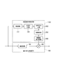
- the receiving apparatus includes a local laser generator 4001, an optical 90-degree hybrid 4002, a photoelectric conversion unit 4003, an AD converter 4004, a chromatic dispersion compensation unit 4005, an adaptive equalization unit 4006, a frequency offset compensation unit 4007, a phase compensation unit 4008, an error A correction / determination unit 4009 and a client interface 4010 are provided.
- the optical signal input to the receiving device is input to the optical 90-degree hybrid 4002, mixed by the local oscillation laser output from the local laser generator 4001 and the optical 90-degree hybrid 4002, and subjected to homodyne detection or heterodyne detection.
- the optical signal obtained by the detection is converted into a baseband analog electric signal in the photoelectric conversion unit 4003.
- This analog electric signal is digitized by the AD converter 4004 and output to the chromatic dispersion compensator 4005.
- a digital signal output from the AD converter 4004 is a signal indicating a symbol represented by a complex number having an in-phase component I and a quadrature component Q.
- the chromatic dispersion compensation unit 4005 compensates the waveform distortion due to chromatic dispersion for the symbol input from the AD converter 4004.
- the adaptive equalization unit 4006 compensates for distortion caused by linear polarization crosstalk, polarization mode dispersion, or the like for the symbol whose waveform distortion is compensated by the chromatic dispersion compensation unit 4005.
- the frequency offset compensation unit 4007 compensates for the influence of the frequency offset that may occur between the transmission device and the reception device that transmit the optical signal, on the symbol whose distortion has been compensated by the adaptive equalization unit 4006.
- the frequency offset is caused by, for example, a frequency shift between local oscillation lasers used in the transmission device and the reception device.
- the phase compensation unit 4008 compensates the phase of the symbol whose frequency offset is compensated by the frequency offset compensation unit 4007 to reduce the occurrence of phase cycle slip.
- the error correction / determination unit 4009 demodulates the symbol whose phase has been compensated by the phase compensation unit 4008, performs error detection and error correction on the data obtained by the demodulation, and then inputs the data to the client interface 4010.
- the client interface 4010 converts and outputs the data input from the error correction / determination unit 9 according to the signal format and frame configuration used in the device connected to the subsequent stage of the receiving device.
- the digital signal processing unit including the chromatic dispersion compensation unit 4005 to the client interface 4009 receives a received signal obtained by converting the received optical signal into an electrical signal using coherent detection and converting the electrical signal into a digital signal. Entered.
- the reception signal input to the digital signal processing unit is a signal indicating a symbol string in which data is mapped based on a modulation scheme used in the transmission apparatus.
- waveform distortion and noise added by the optical fiber transmission line, transmitter, and receiver are reduced or compensated by the chromatic dispersion compensator 4005 and the adaptive equalizer 4006.
- the phase compensator 4008 to which the present invention is applied aims to estimate and remove or reduce the phase noise superimposed on the carrier wave.
- FIG. 24 is a block diagram illustrating a configuration example of the phase compensation unit 4008 in the present embodiment.
- the phase compensation unit 4008 includes an N-th power circuit 4011, an averaging circuit 4012, an angle calculation circuit 4013, an unwrap circuit 4014, a division circuit 4015, a complex number calculation circuit 4016, a delay circuit 4017, a multiplication circuit 4018, a tap coefficient calculation circuit 4020, and a delay circuit. 4021 and a multiplication circuit 4022.
- the phase compensation unit 4008 further includes a tap coefficient calculation circuit 4020, a delay circuit 4021, and a multiplication circuit 4022, as compared with the conventional phase compensation unit.
- the calculation result in the N-th power circuit 4011 is input to the tap coefficient calculation circuit 4020.
- the tap coefficient calculation circuit 4020 calculates the tap coefficient based on the input calculation result (the symbol raised to the Nth power).
- the calculation result in the N-th power circuit 4011 is input to the delay circuit 4021.
- the delay circuit 4021 gives a delay to the input calculation result, and inputs the calculation result to the multiplication circuit 4022 at the same timing as the corresponding tap coefficient.
- the multiplication circuit 4022 receives the symbol given the delay in the delay circuit 4021 and the tap coefficient calculated by the tap coefficient calculation circuit 4020.
- Multiplier circuit 4022 multiplies the input symbol and the tap coefficient, and outputs the multiplication result to averaging circuit 4012.
- the feedforward tap coefficient calculation circuit 4020 implements a feedforward configuration by using a part of tap coefficients used for carrier phase estimation before X symbols for current carrier phase estimation. For example, the tap coefficient used for carrier phase estimation before X symbols is shifted by X tap, and “1” is set as an initial value for the missing X tap and used for the current phase carrier estimation.
- X is an integer of 1 or more, and the upper limit is approximately the storage length of phase noise.
- the tap coefficient is a real number between 0 and 1.
- the storage length of the phase noise corresponds to the time during which coherency is maintained. For example, coherent time is used as an index indicating the time during which coherency is maintained, and the coherent time is a function of the inverse of the width of the phase noise of the light source.
- phase compensation unit 4008 is referred to as a feedforward configuration in the sense that the phase compensation unit 4008 can handle only the tap shift process without using the carrier phase estimation itself before X symbols.
- FIG. 25 is a diagram showing an example of a constellation map after symbols are raised to the Nth power in the Nth power circuit 4011 in the present embodiment.
- M symbols before and after it are used and are plotted in the figure. These M symbols are then arithmetically added on the complex plane, but the amplitude indicated by each symbol varies due to the influence received during transmission such as noise and interference.
- the carrier estimated phase value may deviate greatly from the true value, which is one of the causes for causing a phase cycle slip.
- FIG. 26 is a block diagram illustrating a configuration example of the tap coefficient calculation circuit 4020 in the present embodiment.
- the tap coefficient calculation circuit 4020 includes buffers 4201 and 4202, (X ⁇ 1) subtractors 4203-2 to 4203-X, (X ⁇ 1) absolute value calculators 4204-2 to 4204-X, and adders. 4205 and a power generator 4206. Symbols input from the N-th power circuit 4011 (FIG. 24) to the tap coefficient calculation circuit 4020 are input to the buffer 4201 and the buffer 4202.
- the buffer 4201 stores the input symbol, and when a new symbol is input, the symbol stored in the symbol is updated.
- the buffer 4202 can store X input symbols. When a new symbol is input, the buffer 4202 deletes the oldest symbol from the stored symbols and stores a new symbol.
- the buffer 4202 is configured with a shift register, for example.
- the subtractor 4203-2 to subtractor 4203-X and the absolute value calculators 4204-2 to 4204-X are respectively the oldest symbol (Xth newest symbol) from the second newest symbol stored in the buffer 4202. ).
- Subtractor 4203-2 calculates the difference between the second most recent symbol stored in buffer 4202 and the symbol stored in buffer 4201, and inputs the calculated difference value to absolute value calculator 4204-2. To do.
- the calculation of the difference between two symbols is, for example, when the two symbols to be calculated are (1 + 2i) and (3 + 4i), respectively, and the difference value between these is ( ⁇ 2-2i) or (2 + 2i).
- i is an imaginary unit. That is, calculating the difference between two symbols represented by complex numbers means subtracting the real part and the imaginary part, respectively.
- the absolute value calculator 4204-2 calculates the absolute value of the input difference value and outputs it to the adder 4205.
- Adder 4205 calculates the sum of the absolute values calculated from absolute value calculators 4204-2 to 4204-X, and inputs the calculated sum to power multiplier 4206.
- the power multiplier 4206 outputs the value obtained by raising the input sum to the power p to the multiplier circuit 4022 (FIG. 24) as a tap coefficient corresponding to the symbol stored in the buffer 4201.
- the tap coefficient calculation circuit 4020 calculates the absolute difference corresponding to the Euclidean distance on the complex plane after calculating the difference between the input symbol and the (X ⁇ 1) previous symbol. A value is calculated, and a value obtained by raising the sum of them to the pth power is output as a tap coefficient for the input symbol.
- the Euclidean distance is calculated based on the newest symbol, but any of X symbols may be used. Note that a predetermined value is used as the power p in the power generator 4206.
- FIG. 27 is a block diagram illustrating a configuration example of the tap coefficient calculation circuit 4020A according to the tenth embodiment.
- Tap coefficient calculation circuit 4020A is used in place of tap coefficient calculation circuit 4020 in phase compensation section 4008 (FIG. 24).
- the tap coefficient calculation circuit 4020A includes a delay unit 4211, a subtracter 4212, an absolute value calculation unit 4213, a buffer 4214, an adder 4215, and a power multiplier 4216.
- a symbol input from the N-th power circuit 4011 (FIG. 24) to the tap coefficient calculation circuit 4020A is input to the delay unit 4211 and the subtractor 4212.
- the delay unit 4211 stores the input symbol, and inputs the symbol immediately before the input symbol to the subtractor 4212.
- the subtractor 4212 calculates a difference value between the symbol input from the N-th power circuit 4011 and the symbol input from the delay unit 4211, and inputs the calculated difference value to the absolute value calculator 4213.
- the absolute value calculator 4213 calculates the absolute value of the difference value input from the subtractor 4212 and outputs it to the buffer 4214.
- the buffer 4214 can store X absolute values calculated by the absolute value calculator 4213. When a new absolute value is calculated, the oldest absolute value is deleted and a new absolute value is deleted. Store absolute value.
- the adder 4215 calculates the sum of absolute values stored in the buffer 4214 and inputs the sum to the power multiplier 4216.
- the power multiplier 4216 outputs a value obtained by raising the input sum to the power p to the multiplication circuit 4022 (FIG. 24) as a tap coefficient corresponding to the input symbol.
- FIG. 28 is a block diagram illustrating a configuration example of the tap coefficient calculation circuit 4020B according to the eleventh embodiment.
- Tap coefficient calculation circuit 4020B is used in place of tap coefficient calculation circuit 4020 in phase compensation section 4008 (FIG. 24).
- the tap coefficient calculation circuit 4020B includes buffers 4221 and 4222, an adder 4223, a divider 4224, a subtractor 4225, an absolute value calculator 4226, and a power multiplier 4227.
- the symbols input from the N-th power circuit 4011 (FIG. 24) to the tap coefficient calculation circuit 4020B are input to the buffers 4221 and 4222. Since the buffers 4221 and 4222 have the same configuration as the buffer 4202 in the ninth embodiment, description thereof is omitted.
- the adder 4223 calculates the sum of X symbols stored in the buffer 4221.
- the divider 4224 divides the sum of X symbols calculated by the adder 4223 by X. This division result corresponds to the center of gravity of the X symbols on the complex plane.
- the subtractor 4225 calculates a difference between the X symbols stored in the buffer 4222 and the calculated center of gravity.
- the subtractor 4225 inputs the calculated difference value to the absolute value calculator 4226.
- the absolute value calculator 4226 calculates the absolute value of the input difference value, and inputs the calculated absolute value to the exponent 4227.
- the power multiplier 4227 multiplies the value obtained by raising the input absolute value to the power p as a tap coefficient for the (X / 2) -th central symbol among the X symbols stored in the buffer 4221. It outputs to 4022 (FIG. 24).
- the tap coefficient calculation circuit 4020B generates a copy of the input X symbols and inputs them to the two branches.
- the center of gravity on the complex plane is calculated by dividing the sum of X symbols input to one branch by X.
- the absolute value of the difference from the center of gravity is calculated, and the Euclidean distance from the center of gravity is calculated.
- a value obtained by raising the calculated Euclidean distance to the pth power is set as a tap coefficient for the central symbol among the X symbols.
- the configuration for calculating the mass centroid as the centroid for the X symbols has been described, but the weighted centroid may be calculated. Further, statistics such as the mode value, median value, and average value in X symbols may be calculated instead of the center of gravity.
- the subtractor 4225 calculates the difference between each of the X symbols stored in the buffer 4222 and the center of gravity, and the power multiplier 4227 calculates the p-th power of the sum of the absolute values of the calculated X difference values. You may do it.
- the tap coefficient instead of calculating the tap coefficient for the central symbol among the X symbols stored in the buffer 4222, the tap coefficient may be calculated for an arbitrary symbol of the X symbols. Good. That is, the tap coefficient may be calculated based on X symbols that are consecutive including the target symbol of the tap coefficient to be calculated.
- FIG. 29 is a block diagram showing a configuration of a tap coefficient calculation circuit 4020C in the twelfth embodiment.
- the tap coefficient calculation circuit 4020C is used in place of the tap coefficient calculation circuit 4020 in the phase compensation unit 8 (FIG. 24).
- the tap coefficient calculation circuit 4020C includes buffers 4231 and 4232, X coefficient multipliers 4233-1 to 4233-X, an adder 4234, an angle calculator 4235, and a threshold value determiner 4236. Symbols input from the N-th power circuit 4011 (FIG. 24) to the tap coefficient calculation circuit 4020C are input to the buffers 4231 and 4232. Since the buffers 4231 and 4232 have the same configuration as the buffer 4202 in the ninth embodiment, description thereof is omitted.
- the coefficient multipliers 4233-1 to 4233 -X are provided corresponding to X symbols stored in the buffer 4231.
- the coefficient multiplier 4233-1 corresponds to the newest symbol among the X symbols
- the coefficient multipliers 4233-2 to 4233 -X correspond to the second newest symbol to the Xth symbol.
- Coefficient multiplier 4233-1 multiplies a newest symbol by a predetermined tap coefficient, for example, 1 and outputs the result to adder 4234.
- the coefficient multiplier 4233-2 multiplies the second new symbol by the tap coefficient determined by the threshold value determiner 4236 for the previous symbol and outputs the result to the adder 4234.
- the coefficient multiplier 4233-i multiplies the corresponding symbol in the buffer 4231 by the tap coefficient and outputs the result to the adder 4234.
- the adder 4234 calculates the sum of the multiplication results output from the coefficient multipliers 4233-1 to 4233 -X, and inputs the calculated sum to the angle calculator 4235.
- the sum calculated by the adder 4234 is a symbol indicating a weighted centroid obtained by weighting X symbols with tap coefficients.
- the angle calculator 4235 calculates the deflection angle of the symbol input from the adder 4234, and inputs the calculated deflection angle to the threshold value determination device 4236.
- the threshold determination unit 4236 determines a symbol stored in the buffer 4232 using the deviation angle input from the angle calculator 4235 as a reference angle. The determination by the threshold determination unit 4236 is performed by calculating the deflection angle of the symbol stored in the buffer 4232 and determining whether the calculated deflection angle is more than the threshold angle from the reference angle.
- the threshold determination unit 4236 sets the tap coefficient to 0 when the calculated declination is more than the threshold angle from the reference angle, and sets the tap coefficient when the calculated declination is not more than the threshold angle from the reference angle. Set to 1.
- the tap coefficient determined by the threshold determination unit 4236 is output to the multiplier circuit 4022 (FIG. 24) and also to the coefficient multiplier 4233-2.
- the tap coefficient calculation circuit 4020C takes a copy of the input X symbols and inputs them to the two branches.
- X symbols are multiplied by tap coefficients used for carrier phase estimation one symbol before. Thereafter, the sum of the multiplication results is taken to calculate the deflection angle.
- the calculated declination angle is used as a reference angle for the symbol input to the other branch.
- the threshold value determination unit 4236 determines whether or not the declination angle is more than the threshold angle from the reference angle for each input symbol. Output as.
- the output tap coefficient is used for carrier phase estimation of the current symbol.
- the tap coefficient is inherited as a tap coefficient in order to calculate the reference angle of the next symbol.
- the threshold angle is determined according to, for example, the line width of transmission laser light or reception station light emission (spread of the spectrum in the frequency domain), and may be a variable value.
- FIG. 30 is a block diagram showing a configuration of a tap coefficient calculation circuit 4020D in the thirteenth embodiment.
- Tap coefficient calculation circuit 4020D is used in place of tap coefficient calculation circuit 4020 in phase compensation section 4008 (FIG. 24).
- the tap coefficient calculation circuit 4020D includes a buffer 4241, a distance calculator 4242, a sort circuit 4243, and a tap coefficient determination unit 4244. Symbols input to the tap coefficient calculation circuit 4020D from the N-th power circuit 4011 (FIG. 24) are input to the buffer 4241. Since the buffer 4241 has the same configuration as the buffer 4202 in the ninth embodiment, a description thereof will be omitted.
- the distance calculator 4242 calculates (X ⁇ 1) difference values (Euclidean distance) from the X symbols stored in the buffer 4241, and sorts the calculated (X ⁇ 1) difference values into the sort circuit 4243. To enter.
- the calculation of (X ⁇ 1) difference values in the distance calculator 4242 is performed in the same manner as the difference value calculation in the tap coefficient calculation circuit 4020 of the ninth embodiment, for example. That is, the difference from other (X ⁇ 1) symbols is calculated with the newest symbol as a reference. Alternatively, the difference value may be calculated between adjacent symbols in the same manner as the difference value calculation in the tap coefficient calculation circuit 4020A of the tenth embodiment. Further, similarly to the calculation of the difference value in the tap coefficient calculation circuit 4020B of the eleventh embodiment, the centroid of the X symbols is calculated, and the X difference values are calculated from the calculated centroid and the X symbols. You may do it.
- the sort circuit 4243 sorts (X ⁇ 1) difference values input from the distance calculator 4242 in ascending order.
- the sort circuit 4243 adds an identification number indicating which order the difference value is the difference value corresponding to the input symbol to the difference value, and outputs it to the tap coefficient determination unit 4244.
- the tap coefficient determination unit 4244 sets the tap coefficient for the upper K symbols having a large difference value to 0, and sets the tap coefficient for the other symbols (lower (X-1-K) symbols) to 1.
- the tap coefficient determination unit 4244 rearranges the determined tap coefficients in accordance with the order of the symbols based on the identification number added to the difference value, and then sequentially outputs them to the multiplication circuit 4022 (FIG. 24).
- the Euclidean distance is calculated by the distance calculator 4242 for the M input symbols, and the top K pieces when the Euclidean distance is rearranged in ascending order.
- the tap coefficient for the Euclidean distance is output as 0, and the tap coefficient for the lower (X-1-K) Euclidean distances is output as 1.
- the tap coefficient determination unit 4244 sets the tap coefficient for the symbol corresponding to the upper K difference values to 0, and the lower (X ⁇ K) differences.
- the tap coefficient for the symbol corresponding to the value is set to 1.
- the tap coefficient determination unit 4244 may output the tap coefficient for the newest symbol to the multiplication circuit 4022 (FIG. 24) without outputting a plurality of tap coefficients.
- the tap coefficient determination unit 4244 may output the tap coefficient for the symbol stored at a predetermined position in the buffer 4241 to the multiplication circuit 4022 (FIG. 24).
- FIG. 31 is a block diagram showing a configuration of a tap coefficient calculation circuit 4020E in the fourteenth embodiment.
- Tap coefficient calculation circuit 4020E is used in place of tap coefficient calculation circuit 4020 in phase compensation section 4008 (FIG. 24).
- the tap coefficient calculation circuit 4020E includes a buffer 4251, a distance calculator 4252, a sort circuit 4253, an array buffer 4254, phase estimators 4255 and 4256, a subtractor 4257, an absolute value calculator 4258, and a tap coefficient determiner 4259. ing. Symbols input from the N-th power circuit 4011 (FIG. 24) to the tap coefficient calculation circuit 4020E are input to the buffer 4251 and the array buffer 4254. Since the buffer 4251 has the same configuration as the buffer 4202 in the ninth embodiment, the description thereof is omitted.
- the distance calculator 4252 calculates (X ⁇ 1) difference values (Euclidean distances) from the X symbols stored in the buffer 4251, similarly to the distance calculator 4242 in the thirteenth embodiment.
- the distance calculator 4252 inputs the calculated (X ⁇ 1) Euclidean distances to the sort circuit 4253.
- the sort circuit 4253 sorts the Euclidean distances input from the distance calculator 4252 in ascending order.
- the sort circuit 4253 adds an identification number indicating which Euclidean distance is the Euclidean distance corresponding to the input symbol to the Euclidean distance and inputs it to the array buffer 4254.
- the array buffer 4254 can store X input symbols. When a new symbol is input, the array buffer 4254 deletes the oldest symbol from the stored symbols and stores the new symbol.
- the array buffer 4254 stores the Euclidean distances rearranged by the sort circuit 4253.
- the arrangement buffer 4254 rearranges (X ⁇ 1) symbols out of the stored X symbols in accordance with the stored Euclidean distance.
- the (X-1) symbols to be rearranged are (X-1) symbols excluding either the newest symbol or the oldest symbol among the X symbols.
- the distance calculator 4252 calculates X difference values (Euclidean distance)
- the array buffer 4254 rearranges the input X symbols.
- the phase estimator 4255 performs phase estimation using the top K symbols having a large difference value among the symbols stored in the arrangement buffer 4254 and rearranged. Specifically, the average of K symbols is calculated, and the deviation angle of the average value is calculated. The declination is calculated by arctan (Q / I) where I is the in-phase component of the average value and Q is the quadrature component.
- the phase estimator 4256 performs phase estimation using the symbols stored in the arrangement buffer 4254 and rearranged, and the higher-order (K + 1) symbols having the larger difference values.
- the subtractor 4257 calculates an angle difference between the phase estimation angle calculated by the phase estimator 4255 and the phase estimation angle calculated by the phase estimator 4256.
- the subtractor 4257 inputs the calculated angle difference to the absolute value calculator 4258.
- the absolute value calculator 4258 calculates the absolute value of the angle difference input from the subtractor 4257, and inputs the calculated absolute value to the tap coefficient determiner 4259.
- the tap coefficient determination unit 4259 compares the absolute value input from the absolute value calculator 4258 with a predetermined angle threshold value ⁇ .
- the tap coefficient determination unit 4259 determines 0 as the tap coefficient if the absolute value is greater than or equal to the angle threshold ⁇ , and determines 1 as the tap coefficient if the absolute value is less than the angle threshold ⁇ .
- Tap coefficient determination unit 4259 outputs the determined tap coefficient to multiplication circuit 4022 (FIG. 24).
- the tap coefficient output from the tap coefficient determination unit 4259 is, for example, a symbol corresponding to the newest symbol among symbols input to the tap coefficient calculation circuit 4020E.
- the angle threshold value ⁇ used in the tap coefficient determination unit 4259 is (360 ° / m) when the modulation method used in the transmission system is m-PSK.
- the angle threshold value ⁇ is determined according to how many symbol points exist on the same circumference on the constellation plane. For example, when the modulation method is 16QAM, the angle threshold value ⁇ is set to 90 ° for the symbols present on the innermost and outermost circles on the constellation plane, On the other hand, the angle threshold value ⁇ is set to 45 °.
- the input X symbols are duplicated and input to the two branches.
- the Euclidean distance on the complex plane is calculated for X input symbols.
- the calculated Euclidean distances are rearranged in ascending order by the sort circuit 4253 and stored in the array buffer 4254.
- the X symbols input to the other branch are rearranged corresponding to the Euclidean distance stored in the array buffer 4254.
- the phase estimation angle calculated by the phase estimator 4255 using the upper K symbols and the phase estimation angle calculated by the phase estimator 4256 using the upper (K + 1) symbols are subtracted.
- the absolute value of the angle difference as a subtraction result is input to the tap coefficient determination unit 4259.
- the tap coefficient determination unit 4259 outputs 0 as the tap coefficient if the angle difference is more than the angle threshold value ⁇ , and 1 otherwise as the tap coefficient.
- FIG. 32 is a block diagram illustrating a configuration example of the phase compensation unit 4008A according to the fifteenth embodiment.
- the phase compensation unit 4008A is used in place of the phase compensation unit 4008 in the digital signal processing unit (FIG. 23).
- the phase compensation unit 4008A includes an N-th power circuit 4011, an averaging circuit 4012, an angle calculation circuit 4013, an unwrap circuit 4014, a division circuit 4015, a complex number calculation circuit 4016, a delay circuit 4017, a multiplication circuit 4018, a tap coefficient calculation circuit 4030, and a delay circuit. 4031 and a multiplication circuit 4032 are provided.
- the phase compensation unit 4008A further includes a tap coefficient calculation circuit 4030, a delay circuit 4031, and a multiplication circuit 4032 as compared with the conventional phase compensation unit.
- the carrier phase estimation value calculated by the division circuit 4015 is input to the tap coefficient calculation circuit 4030 after being given a predetermined delay by the delay circuit 4031.
- Tap coefficient calculation circuit 4030 calculates a tap coefficient based on the input carrier phase estimation value.
- the multiplication circuit 4032 receives the calculation result (N-th power symbol) in the N-th power circuit 4011 and the tap coefficient calculated by the tap coefficient calculation circuit 4030.
- the multiplication circuit 4032 multiplies the N-th power symbol and the tap coefficient, and outputs the multiplication result to the averaging circuit 4012.
- the N-th power symbol input to the multiplication circuit 4032 is multiplied by a tap coefficient obtained using the carrier phase estimation value calculated based on the X symbols preceding the symbol.
- the delay amount in the delay circuit 4031 is set.
- another delay circuit is provided between the N-th power circuit 4011 and the multiplication circuit 4032, and the timing at which the N-th power symbol is input to the multiplication circuit 4032 and the tap coefficient are supplied to the multiplication circuit 4032. You may make it align with the timing inputted.
- the phase compensation unit 4008A in this embodiment is a feedback type, and includes a tap coefficient calculation circuit 4030, a multiplication circuit 4032 that multiplies each of the symbols, and a delay circuit 4031.
- Feedback type tap coefficient calculation circuit 4030 calculates the tap coefficient based on the information of the carrier phase estimation value before X symbols. In the present specification, this is called a feedback configuration in the sense that the carrier phase estimation value itself before X symbols is used.
- FIG. 33 is a block diagram illustrating a configuration example of the tap coefficient calculation circuit 4030 in the present embodiment.
- the tap coefficient calculation circuit 4030 includes a delay unit 4301 and a tap coefficient determination unit 4302.
- the carrier phase estimation value input from division circuit 4015 (FIG. 32) to tap coefficient calculation circuit 4030 is input to delay unit 4301.
- the delay unit 4301 gives a delay of one symbol to the input carrier phase estimation value, and then outputs the carrier phase estimation value to the tap coefficient determination unit 4302.
- the N-th power symbol input from the N-th power circuit 11 (FIG. 32) to the tap coefficient calculation circuit 4030 is input to the tap coefficient determination unit 4302.
- Tap coefficient determination unit 4302 calculates the deviation angle of the input N-th power symbol, and compares the calculated deviation angle with the carrier phase estimation value.
- the tap coefficient determination unit 4302 determines whether or not the calculated declination and the carrier phase estimation value have a difference greater than or equal to the angle threshold value ⁇ . Is set to 0.
- the tap coefficient determination unit 4302 sets the tap coefficient to 1 when the difference is less than the angle threshold value ⁇ .
- Tap coefficient determination unit 4302 outputs the determined tap coefficient to multiplication circuit 4032 (FIG. 32).
- the input symbol is determined by the tap coefficient determination unit 4302 with reference to the carrier phase estimation value one symbol before.
- the tap coefficient determination unit 4302 determines whether or not the deviation angle of the input symbol is away from the carrier phase estimation value by an angle threshold value ⁇ or more. If it is away, 0 is set. If not, 1 is set. Determined as tap coefficient.
- the angle threshold value ⁇ is 0 degree or more and less than 360 degrees.
- the tap coefficient is determined based on the carrier phase estimation value of one symbol before.
- any carrier phase estimation value may be used as long as it is a carrier phase estimation value corresponding to a symbol within a period having a phase relationship. May be used as a reference.
- FIG. 34 is a block diagram illustrating a configuration example of the preprocessing circuit 4040 in the modification.
- the preprocessing circuit 4040 includes a power generator 4401, a delay unit 4402, and a multiplier 4403. Symbols input from the N-th power circuit 4011 (symbols raised to the Nth power) are input to the power generator 4401 and the delay device 4402.
- the power multiplier 4401 calculates the p-th power of the absolute value of the input symbol and inputs the calculation result to the multiplier 4403 as a tap coefficient.
- the delay unit 4402 gives the input symbol to the multiplier 4403 after giving the input symbol a delay corresponding to the time required for the operation in the exponent 4401.
- Multiplier 4403 multiplies the input symbol and the tap coefficient, and outputs the multiplication result to tap coefficient calculation circuit 4020 (or tap coefficient calculation circuit 4030).
- the tap coefficient calculation circuit 4020 calculates the tap coefficient for the symbols output from the preprocessing circuit 40 by the processing described in the ninth to fifteenth embodiments. It will be.
- FIG. 35 is a block diagram illustrating a configuration example of the phase compensation unit 4008B according to the sixteenth embodiment.
- the phase compensation unit 4008B is used in place of the phase compensation unit 8 in the digital signal processing unit (FIG. 23).
- the phase compensation unit 4008B includes a complex number calculation circuit 4016, a delay circuit 4017, a multiplication circuit 4018, and a phase averaging circuit 4050. Symbols sequentially input from the frequency offset compensator 4007 to the phase compensator 4008B are input to the delay circuit 4017 and the phase averaging circuit 4050.
- the phase averaging circuit 4050 calculates the average of the phases of symbols included in a period with phase correlation based on the input symbols.
- the phase averaging circuit 4050 calculates the average of the symbol phases using an exponential average that calculates an average with a coefficient corresponding to the time at which the phase correlation decreases.
- the phase averaging circuit 4050 calculates the average ⁇ (i) of the phase of the symbol when the i-th symbol is input, the phase ⁇ (i) of the i-th symbol, the coefficient ⁇ , and the coefficient Calculate using ⁇ .
- the coefficient ⁇ is a coefficient corresponding to a decrease in the coherency of the light source, and is an exponential average that attenuates the contribution in the average of the phase of the past symbols.
- the coefficient ⁇ is multiplied by symbols that are greatly affected by transmission such as noise and interference and other symbols. It is assumed that 0 ⁇ ⁇ ⁇ 1 for a symbol that is greatly affected, and ⁇ 1 for other symbols.
- the phase averaging circuit 4050 calculates an average ⁇ (i) of symbol phases using the following equation (5).
- ⁇ (i) ⁇ (i) ⁇ ⁇ ⁇ ⁇ + (1 ⁇ ) ⁇ ⁇ (i ⁇ 1) (5)
- Equation (6) and (7) may be used as exponential averages for adding the average of the phases at that time.
- ⁇ (i) ⁇ (i) ⁇ ⁇ + (1 ⁇ ) ⁇ ⁇ (i ⁇ 1) (6)
- ⁇ (i) ⁇ (i ⁇ 1) ⁇ ⁇ + (1 ⁇ ) ⁇ ⁇ (i ⁇ 1) (7)
- the phase compensator having the configuration described in each embodiment determines the reference of the symbol by suppressing the influence of the symbol that is greatly affected by noise and interference among the symbols included in the period having the phase correlation.
- the phase is estimated by reducing the influence of Gaussian noise or the like.
- the occurrence of phase cycle slip can be reduced.
- outlier detection becomes easy, so the weight coefficient for a symbol that is greatly affected by noise or interference can be increased,
- the phase can be estimated with high accuracy by excluding it.
- the phase compensation unit targets symbols in a period with phase correlation in the process of suppressing the influence of symbols (outliers) that are greatly affected by noise and interference, and therefore has a phase relationship with the current symbol. And the influence of outliers can be reduced with high accuracy.
- the frequency of occurrence of phase cycle slips can be reduced without increasing the bit error rate or reducing the transmission efficiency. Can be reduced.
- the phase averaging circuit 4050 may calculate a moving average of measured values in a time corresponding to a phase relationship, for example, a period corresponding to a coherent time, as an average ⁇ (i) of symbol phases.
- FIG. 36 is a diagram showing an outline of an experimental apparatus used for obtaining the optical transmission experimental data.
- FIG. 37 is a graph showing the evaluation results of the phase cycle slip ratio corresponding to the phase compensation unit 4008A in the fifteenth embodiment.
- the vertical axis represents the phase cycle slip ratio
- the horizontal axis represents the average window width M.
- the graph shown by the A method in the figure is a result shown as a comparative example, and is a result of a computer simulation using a conventional phase compensator.
- the graph shown by the B method is a computer simulation result using the phase compensation unit 4008A in the fifteenth embodiment.
- the angle threshold value ⁇ is ⁇ 45 °.
- FIG. 37 it can be seen that the frequency of occurrence of phase cycle slip can be reduced to about 1/3 by applying the phase compensation unit in the present embodiment.
- the configuration for calculating the tap coefficient without using a known signal such as a pilot symbol has been described.
- a compensation method estimated using a pilot symbol or the like may be used in combination.
- the phase estimated by the pilot symbol may be used for calculating the tap coefficient.
- likelihood information or the like may be added as a weight and averaged.
- the configuration using four-phase phase (QPSK) modulation is described as an example of the modulation method. Phase modulation may be used.
- N the power number
- ⁇ the angle threshold value ⁇ are determined according to the modulation method to be used.
- the configuration in which the phase component excluding the phase modulation component of the data is extracted using the N-th power circuit 4011 has been described.
- the phase component using a method other than this, for example, the maximum likelihood determination method or the like. May be extracted.
- the determination of whether or not the angle difference is greater than or equal to the angle threshold value ⁇ is used for the determination when determining the tap coefficient.
- the present invention is not limited to this.
- the deviation from the reference angle of the symbol phase excluding the phase modulation component of the data is greater than or equal to the sum of the phase noise of either the signal light at the transmitting device or the local light at the receiving device, or both. It may be used for the determination.
- a configuration has been described in which the phase of a symbol that is greatly affected by noise or interference, that is, the phase of a symbol that has a large Euclidean distance is multiplied by a coefficient of 0 (zero) or less than 1 and added.
- the present invention is not limited to this.
- a reference angle may be added instead of the phase of a symbol having a large Euclidean distance.
- each functional unit provided in the reception device is configured by a plurality of devices, and each device is configured via a network. You may be connected so that communication is possible.
- each functional unit of the digital signal processing unit may be configured by a plurality of devices. Further, the period (X symbol) with phase correlation in each embodiment and the value of the averaging window width M may be matched.
- a program for realizing the functions of the digital signal processing unit shown in FIG. 23 is recorded on a computer-readable recording medium, and the program recorded on the recording medium is read into a computer system and executed.
- the processing performed by the digital signal processing unit for example, the phase compensation unit may perform phase compensation to reduce phase cycle slip.
- the “computer system” includes an OS and hardware such as peripheral devices.
- the “computer system” includes a WWW system having a homepage providing environment (or display environment).
- the “computer-readable recording medium” refers to a storage device such as a flexible medium, a magneto-optical disk, a portable medium such as a ROM or a CD-ROM, and a hard disk incorporated in a computer system.
- the “computer-readable recording medium” refers to a volatile memory (RAM) in a computer system that becomes a server or a client when a program is transmitted via a network such as the Internet or a communication line such as a telephone line. In addition, those holding programs for a certain period of time are also included.
- RAM volatile memory
- the program may be transmitted from a computer system storing the program in a storage device or the like to another computer system via a transmission medium or by a transmission wave in the transmission medium.
- the “transmission medium” for transmitting the program refers to a medium having a function of transmitting information, such as a network (communication network) such as the Internet or a communication line (communication line) such as a telephone line.
- the program may be for realizing a part of the functions described above. Furthermore, what can implement
- the present invention can reduce the influence of the occurrence of phase cycle slip in long-distance and large-capacity optical communication.
- the present invention can be applied to, for example, large-capacity and long-distance optical transmission in which a transmission distance is about 100 km to 10,000 km and a transmission capacity per channel is about 40 Gb / s to 400 Gb / s.
- SYMBOLS 1 ... Carrier phase estimation part, 2 ... Carrier phase compensation part, 3 ... Delay difference part, 4 ... Slip determination part, 5 ... Slip compensation part, 11 ... Optical signal transmitter, 12 ... Transmission path, 13 ... Optical signal receiver , 14 ... Local laser generator, 15 ... 90 ° optical hybrid, 16 ... Photoelectric converter, 17 ... Analog-to-digital converter, 18 ... Digital signal processor, 19 ... Wavelength dispersion compensation circuit, 20 ... Adaptive equalization circuit , 21 ... frequency offset compensation circuit, 22 ... phase compensation circuit, 23 ... demodulation decoding circuit, 24 ... client interface, 220, 320, 420, 520 ... phase compensation block, 221 ...
- carrier phase estimation circuit 222 ... carrier phase compensation circuit 223, delay circuit, 224, low-pass filter, 225, 225-1, 225-2, 225-3, delay difference circuit, 226, 326 426 ... slip determination circuit, 227 ... slip compensation circuit, 328 ... threshold calculation circuit, 527 ... slip transient compensation circuit, 528 ... slope calculation circuit, 2211 ... phase m multiplication circuit, 2212 ... K symbol averaging circuit, 2213 ... phase extraction Circuit, 2214 ... Phase continuation circuit, 2251 ... N symbol delay, 2252, 3281, 3283 ... Multiplier, 2253, 3282, 3285 ... Adder, 3284 ... Delay, 3286 ... Subtractor, 22111 ...
- Amplitude / phase separation Circuit 22112... Multiplier, 22113... Amplitude / phase recombination circuit, 4001 ... Local oscillator laser generator, 4002 ... Optical 90-degree hybrid, 4003 ... Photoelectric conversion unit, 4004 ... AD converter, 4005 ... Wavelength dispersion compensation unit, 4006 ... Adaptive equalization unit, 4007 ... Frequency offset compensation unit, 4008, 4008A , 4008B ... Phase compensation unit, 4009 ... Error correction / determination unit, 4010 ... Client interface, 4011 ... N-th power circuit, 4012 ... Averaging circuit, 4013 ... Angle calculation circuit, 4014 ... Unwrap circuit, 4015 ... Division circuit, 4016 ...
- Complex number calculation circuit 4017, 4021, 4031 ... delay circuit, 4018, 4022, 4032 ... multiplication circuit 4020, 4020A, 4020B, 4020C, 4020D, 4020E, 4030 ... tap coefficient calculation circuit, 4040 ... preprocessing circuit, 4050 ... phase average Circuit.
Landscapes
- Engineering & Computer Science (AREA)
- Computer Networks & Wireless Communication (AREA)
- Signal Processing (AREA)
- Physics & Mathematics (AREA)
- Electromagnetism (AREA)
- Optics & Photonics (AREA)
- Optical Communication System (AREA)
- Digital Transmission Methods That Use Modulated Carrier Waves (AREA)
Abstract
Priority Applications (4)
| Application Number | Priority Date | Filing Date | Title |
|---|---|---|---|
| EP14742856.9A EP2930867B1 (fr) | 2013-01-25 | 2014-01-24 | Dispositif récepteur optique et procédé de réduction du glissement de cycle de phase |
| US14/758,941 US9667350B2 (en) | 2013-01-25 | 2014-01-24 | Optical receiving device and phase cycle reduction method |
| JP2014558630A JP5886984B2 (ja) | 2013-01-25 | 2014-01-24 | 光受信装置および位相サイクルスリップ低減方法 |
| CN201480005832.0A CN104919729B (zh) | 2013-01-25 | 2014-01-24 | 光接收装置和相位周跳减少方法 |
Applications Claiming Priority (4)
| Application Number | Priority Date | Filing Date | Title |
|---|---|---|---|
| JP2013-012403 | 2013-01-25 | ||
| JP2013012403 | 2013-01-25 | ||
| JP2013-036126 | 2013-02-26 | ||
| JP2013036126 | 2013-02-26 |
Publications (1)
| Publication Number | Publication Date |
|---|---|
| WO2014115840A1 true WO2014115840A1 (fr) | 2014-07-31 |
Family
ID=51227629
Family Applications (1)
| Application Number | Title | Priority Date | Filing Date |
|---|---|---|---|
| PCT/JP2014/051501 WO2014115840A1 (fr) | 2013-01-25 | 2014-01-24 | Dispositif récepteur optique et procédé de réduction du glissement de cycle de phase |
Country Status (5)
| Country | Link |
|---|---|
| US (1) | US9667350B2 (fr) |
| EP (1) | EP2930867B1 (fr) |
| JP (1) | JP5886984B2 (fr) |
| CN (1) | CN104919729B (fr) |
| WO (1) | WO2014115840A1 (fr) |
Cited By (4)
| Publication number | Priority date | Publication date | Assignee | Title |
|---|---|---|---|---|
| WO2016035895A1 (fr) * | 2014-09-03 | 2016-03-10 | Mitsubishi Electric Corporation | Système et procédé de récupération de phase de porteuse dans des communications optiques |
| JP2017153013A (ja) * | 2016-02-26 | 2017-08-31 | 三菱電機株式会社 | 受信装置及び受信方法 |
| JP2018042219A (ja) * | 2016-09-09 | 2018-03-15 | 富士通株式会社 | 受信装置及び位相誤差補償方法 |
| WO2019043856A1 (fr) | 2017-08-31 | 2019-03-07 | 三菱電機株式会社 | Dispositif de transmission/réception optique et procédé de transmission/réception optique |
Families Citing this family (13)
| Publication number | Priority date | Publication date | Assignee | Title |
|---|---|---|---|---|
| US10038507B2 (en) * | 2013-02-13 | 2018-07-31 | Nippon Telegraph And Telephone Corporation | Optical transmission system, phase compensation method, and optical reception apparatus |
| JP2016144197A (ja) * | 2015-02-05 | 2016-08-08 | 日本電信電話株式会社 | 光信号受信機、光信号受信方法及び光伝送システム |
| JP6485095B2 (ja) * | 2015-02-18 | 2019-03-20 | 富士通株式会社 | 光伝送装置、光伝送システム、及び、偏波依存損失モニタ |
| CN106501604B (zh) * | 2016-10-24 | 2019-03-19 | 中国科学院上海应用物理研究所 | 一种测量粒子加速器束团纵向相位的方法 |
| JP2018129618A (ja) * | 2017-02-07 | 2018-08-16 | 富士通株式会社 | 受信装置および受信方法 |
| CN106953826B (zh) * | 2017-04-12 | 2020-07-31 | 广西师范大学 | 一种ofdm信号差分接收方法 |
| CN109728856B (zh) * | 2017-10-27 | 2021-12-31 | 富士通株式会社 | 光发射机iq不平衡的估计装置、补偿装置及电子设备 |
| US11582019B2 (en) * | 2018-11-29 | 2023-02-14 | Nippon Telegraph And Telephone Corporation | Receiving apparatus, receiving method and program |
| JP7055253B2 (ja) * | 2019-08-26 | 2022-04-15 | 三菱電機株式会社 | 受信器 |
| US11038598B1 (en) | 2020-02-26 | 2021-06-15 | Huawei Technologies Co., Ltd. | Method and apparatus for transmit/receive radio frequency crosstalk compensation in a photonic integrated circuit |
| GB2602353B (en) * | 2020-12-24 | 2023-09-13 | Toshiba Kk | Optical system and method |
| CN112787723B (zh) * | 2020-12-29 | 2022-03-25 | 武汉邮电科学研究院有限公司 | 一种非线性编码器、编码方法及光传输系统 |
| CN114401176B (zh) * | 2021-12-31 | 2023-05-09 | 北京升哲科技有限公司 | 一种信号到达检测方法、装置、电子设备及存储介质 |
Citations (3)
| Publication number | Priority date | Publication date | Assignee | Title |
|---|---|---|---|---|
| JP2011166597A (ja) * | 2010-02-12 | 2011-08-25 | Mitsubishi Electric Corp | 搬送波位相補正回路 |
| WO2012111847A1 (fr) * | 2011-02-17 | 2012-08-23 | 日本電気株式会社 | Circuit de traitement de signal, procédé de traitement de signal, récepteur optique et système de communication optique |
| WO2012132103A1 (fr) * | 2011-03-25 | 2012-10-04 | 日本電気株式会社 | Récepteur à compensation de phase |
Family Cites Families (11)
| Publication number | Priority date | Publication date | Assignee | Title |
|---|---|---|---|---|
| ATE350846T1 (de) * | 2003-09-05 | 2007-01-15 | Europ Agence Spatiale | Verfahren zur pilotgestützen trägerphasensynchronisation |
| JP4918400B2 (ja) * | 2007-04-27 | 2012-04-18 | 富士通株式会社 | 光信号受信装置 |
| US8311417B1 (en) * | 2008-11-25 | 2012-11-13 | Cisco Technology, Inc. | Decision directed carrier phase estimation with a limiter for coherent dense wavelength division multiplexing systems |
| US8166365B2 (en) | 2008-12-03 | 2012-04-24 | Ciena Corporation | Cycle slip location and correction |
| JP5287516B2 (ja) * | 2009-05-29 | 2013-09-11 | 富士通株式会社 | デジタルコヒーレント光受信器 |
| CA2765362C (fr) * | 2009-06-17 | 2017-09-26 | Huawei Technologies Co., Ltd. | Procede de recuperation de frequence porteuse et recepteur optique coherent intradyne |
| US8718203B2 (en) * | 2010-03-16 | 2014-05-06 | Anchor Hill Communications, Llc | Single carrier communication in dynamic fading channels |
| EP2381595B1 (fr) * | 2010-04-21 | 2012-06-20 | Alcatel Lucent | Compensation de l'obliquité de phase dans un récepteur optique cohérent |
| US9083471B2 (en) * | 2011-03-03 | 2015-07-14 | Technion Research And Development Foundation Ltd. | Coherent and self-coherent signal processing techniques |
| CN102820929B (zh) * | 2012-08-24 | 2015-04-15 | 武汉邮电科学研究院 | 光相干接收装置中的相位估计方法 |
| US9112615B1 (en) * | 2013-01-23 | 2015-08-18 | Viasat, Inc. | Low cycle slip phase recovery for coherent receiver |
-
2014
- 2014-01-24 CN CN201480005832.0A patent/CN104919729B/zh active Active
- 2014-01-24 JP JP2014558630A patent/JP5886984B2/ja active Active
- 2014-01-24 WO PCT/JP2014/051501 patent/WO2014115840A1/fr active Application Filing
- 2014-01-24 US US14/758,941 patent/US9667350B2/en active Active
- 2014-01-24 EP EP14742856.9A patent/EP2930867B1/fr active Active
Patent Citations (3)
| Publication number | Priority date | Publication date | Assignee | Title |
|---|---|---|---|---|
| JP2011166597A (ja) * | 2010-02-12 | 2011-08-25 | Mitsubishi Electric Corp | 搬送波位相補正回路 |
| WO2012111847A1 (fr) * | 2011-02-17 | 2012-08-23 | 日本電気株式会社 | Circuit de traitement de signal, procédé de traitement de signal, récepteur optique et système de communication optique |
| WO2012132103A1 (fr) * | 2011-03-25 | 2012-10-04 | 日本電気株式会社 | Récepteur à compensation de phase |
Non-Patent Citations (2)
| Title |
|---|
| A. J. VITERBI; A. M. VITERBI: "Nonlinear Estimation of PSK-Modulated Carrier Phase with Application to Burst Digital Transmission", IEEE TRANS. ON INFO. THEORY, vol. IT-29, July 1983 (1983-07-01), XP000760812, DOI: doi:10.1109/TIT.1983.1056713 |
| KAZUYOSHI ITOH ET AL., APPLIED OPTICS, vol. 21, no. 14 /15, July 1982 (1982-07-01) |
Cited By (11)
| Publication number | Priority date | Publication date | Assignee | Title |
|---|---|---|---|---|
| WO2016035895A1 (fr) * | 2014-09-03 | 2016-03-10 | Mitsubishi Electric Corporation | Système et procédé de récupération de phase de porteuse dans des communications optiques |
| US9473250B2 (en) | 2014-09-03 | 2016-10-18 | Mitsubishi Electric Research Laboratories, Inc. | System and method for recovering carrier phase in optical communications |
| CN106797256A (zh) * | 2014-09-03 | 2017-05-31 | 三菱电机株式会社 | 在光通信中恢复载波相位的系统和方法 |
| JP2017520974A (ja) * | 2014-09-03 | 2017-07-27 | 三菱電機株式会社 | 光通信において搬送波位相を再生するためのシステム及び方法 |
| CN106797256B (zh) * | 2014-09-03 | 2019-06-11 | 三菱电机株式会社 | 在光通信中恢复载波相位的系统和方法 |
| JP2017153013A (ja) * | 2016-02-26 | 2017-08-31 | 三菱電機株式会社 | 受信装置及び受信方法 |
| DE102017202146A1 (de) | 2016-02-26 | 2017-08-31 | Mitsubishi Electric Corporation | Empfangsvorrichtung und Empfangsverfahren |
| DE102017202146B4 (de) | 2016-02-26 | 2021-07-22 | Mitsubishi Electric Corporation | Empfangsvorrichtung und Empfangsverfahren |
| JP2018042219A (ja) * | 2016-09-09 | 2018-03-15 | 富士通株式会社 | 受信装置及び位相誤差補償方法 |
| WO2019043856A1 (fr) | 2017-08-31 | 2019-03-07 | 三菱電機株式会社 | Dispositif de transmission/réception optique et procédé de transmission/réception optique |
| US11088776B2 (en) | 2017-08-31 | 2021-08-10 | Mitsubishi Electric Corporation | Optical transmission/reception device and optical transmission/reception method |
Also Published As
| Publication number | Publication date |
|---|---|
| EP2930867B1 (fr) | 2019-04-24 |
| EP2930867A4 (fr) | 2016-10-26 |
| US9667350B2 (en) | 2017-05-30 |
| JPWO2014115840A1 (ja) | 2017-01-26 |
| CN104919729A (zh) | 2015-09-16 |
| CN104919729B (zh) | 2017-06-20 |
| EP2930867A1 (fr) | 2015-10-14 |
| US20150333838A1 (en) | 2015-11-19 |
| JP5886984B2 (ja) | 2016-03-16 |
Similar Documents
| Publication | Publication Date | Title |
|---|---|---|
| JP5886984B2 (ja) | 光受信装置および位相サイクルスリップ低減方法 | |
| JP5406989B2 (ja) | 光受信器及び光伝送システム | |
| CA3019897C (fr) | Dispositif de compensation de caracteristique de transmission, procede de compensation de caracteristique de transmission et dispositif de communication | |
| US10277328B2 (en) | Signal processing device used in optical receiver and signal processing method | |
| JP5590090B2 (ja) | 周波数オフセット補償装置及び方法並びに光コヒーレント受信機 | |
| US8909068B2 (en) | Skew estimator, skew compensator and coherent receiver | |
| US9240843B1 (en) | Method and apparatus for blind time skew compensation for coherent optical receivers | |
| Li et al. | Wide-range, accurate and simple digital frequency offset compensator for optical coherent receivers | |
| US20090208224A1 (en) | Optical field receiver, optical multilevel signal receiver, and optical transmission system | |
| WO2014126132A1 (fr) | Système de transmission optique, procédé de compensation de phase et dispositif de réception optique | |
| US20140079407A1 (en) | Updating apparatus and method for equalizer coefficient, receiver and otpical communication system | |
| EP2567461B1 (fr) | Procédé et appareil de détection d'une erreur de parité dans une séquence de symboles dqpsk d'un système de transmission numérique | |
| US9455847B1 (en) | Wireless communication apparatus with phase noise mitigation | |
| JP6743603B2 (ja) | 受信装置及び位相誤差補償方法 | |
| JP5312384B2 (ja) | ディジタルサンプル処理方法、ディジタルサンプル処理装置、及びプログラム | |
| JP6540295B2 (ja) | 適応等化回路、ディジタルコヒーレント受信器および適応等化方法 | |
| EP3055936A1 (fr) | Appareil pour caractériser une dispersion chromatique d'un signal reçu optique | |
| JPWO2013124986A1 (ja) | 偏波推定器、偏波分離器、光受信器、偏波推定方法、および、偏波分離方法 | |
| EP2862297B1 (fr) | Récepteur pour système de transmission optique | |
| JP6885343B2 (ja) | ディジタル信号処理回路、及び、光空間通信システム | |
| RU2664019C9 (ru) | Устройство и способ адаптивной компенсации искажений и восстановления несущей сигнала для когерентных приёмников | |
| Su et al. | QPSK assisted carrier phase recovery for high order QAM | |
| Zhou | Carrier recovery in coherent optical communication systems | |
| JP6058682B2 (ja) | デジタル信号処理装置 | |
| WO2017069086A1 (fr) | Dispositif de réception de lumière cohérente |
Legal Events
| Date | Code | Title | Description |
|---|---|---|---|
| 121 | Ep: the epo has been informed by wipo that ep was designated in this application |
Ref document number: 14742856 Country of ref document: EP Kind code of ref document: A1 |
|
| ENP | Entry into the national phase |
Ref document number: 2014558630 Country of ref document: JP Kind code of ref document: A |
|
| WWE | Wipo information: entry into national phase |
Ref document number: 14758941 Country of ref document: US |
|
| WWE | Wipo information: entry into national phase |
Ref document number: 2014742856 Country of ref document: EP |
|
| NENP | Non-entry into the national phase |
Ref country code: DE |