WO2014115451A1 - 圧電振動部品 - Google Patents
圧電振動部品 Download PDFInfo
- Publication number
- WO2014115451A1 WO2014115451A1 PCT/JP2013/084090 JP2013084090W WO2014115451A1 WO 2014115451 A1 WO2014115451 A1 WO 2014115451A1 JP 2013084090 W JP2013084090 W JP 2013084090W WO 2014115451 A1 WO2014115451 A1 WO 2014115451A1
- Authority
- WO
- WIPO (PCT)
- Prior art keywords
- substrate
- electrode
- corner
- piezoelectric vibration
- piezoelectric
- Prior art date
- Legal status (The legal status is an assumption and is not a legal conclusion. Google has not performed a legal analysis and makes no representation as to the accuracy of the status listed.)
- Ceased
Links
Images



Classifications
-
- H—ELECTRICITY
- H03—ELECTRONIC CIRCUITRY
- H03H—IMPEDANCE NETWORKS, e.g. RESONANT CIRCUITS; RESONATORS
- H03H9/00—Networks comprising electromechanical or electro-acoustic elements; Electromechanical resonators
- H03H9/02—Details
- H03H9/05—Holders or supports
- H03H9/10—Mounting in enclosures
- H03H9/1007—Mounting in enclosures for bulk acoustic wave [BAW] devices
- H03H9/1014—Mounting in enclosures for bulk acoustic wave [BAW] devices the enclosure being defined by a frame built on a substrate and a cap, the frame having no mechanical contact with the BAW device
- H03H9/1021—Mounting in enclosures for bulk acoustic wave [BAW] devices the enclosure being defined by a frame built on a substrate and a cap, the frame having no mechanical contact with the BAW device the BAW device being of the cantilever type
-
- H—ELECTRICITY
- H03—ELECTRONIC CIRCUITRY
- H03H—IMPEDANCE NETWORKS, e.g. RESONANT CIRCUITS; RESONATORS
- H03H9/00—Networks comprising electromechanical or electro-acoustic elements; Electromechanical resonators
- H03H9/02—Details
- H03H9/02007—Details of bulk acoustic wave devices
- H03H9/02086—Means for compensation or elimination of undesirable effects
Definitions
- the present invention relates to a piezoelectric vibration component in which a piezoelectric vibrator is mounted on a substrate.
- Patent Document 1 discloses an example of this type of piezoelectric vibration component.
- a piezoelectric vibrator is held on a rectangular plate-shaped substrate.
- First and second attachment electrodes for electrically connecting and holding the piezoelectric vibrator are formed on the upper surface of the rectangular plate-shaped substrate.
- a first terminal electrode is formed at one corner of the substrate.
- a first attachment electrode is formed on the first terminal electrode.
- a second terminal electrode is formed at the other corner.
- a second attachment electrode is electrically connected to the second terminal electrode by a wiring electrode.
- a metal cap is fixed to the upper surface of the substrate via an adhesive so as to surround the piezoelectric vibrator.
- An object of the present invention is to provide a piezoelectric vibration component capable of suppressing the influence of external noise.
- the piezoelectric vibration component according to the present invention includes a substrate, first and second attachment electrodes, a piezoelectric vibrator, and a cap made of metal.
- the substrate has an upper surface and a lower surface.
- the substrate is a rectangular plate-like substrate, and the upper surface has first and second sides facing each other and third and fourth sides facing each other.
- the cap is fixed to the substrate so as to surround the piezoelectric vibrator mounted on the substrate, and has an opening opened on the substrate side.
- the first and second attachment electrodes are formed on the upper surface of the substrate.
- the piezoelectric vibrator is electrically and mechanically connected to the first and second mounting electrodes and is held on the upper surface of the substrate.
- a corner portion formed by the first side and the third side is a first corner
- a corner portion formed by the first side and the fourth side is a second corner
- a corner portion formed by the third side is defined as a third corner
- a corner portion formed by the second side and the fourth side is defined as a fourth corner.
- the first attachment electrode is provided closer to the first corner among the first to fourth corners.
- the second attachment electrode is provided near the second corner of the first to fourth corners.
- the piezoelectric vibration component according to the present invention further includes first and second terminal electrodes, first and second wiring electrodes, and a protruding electrode portion.
- the first terminal electrode is provided at the third corner, and the second terminal electrode is provided at the second corner.
- the first wiring electrode is provided on the upper surface of the substrate so as to connect the first attachment electrode and the first terminal electrode.
- the second wiring electrode is provided on the upper surface of the substrate so as to connect the second attachment electrode and the second terminal electrode.
- the protruding electrode portion extends from the second mounting electrode toward the fourth corner side on the upper surface of the substrate so as to be electrically connected to the second mounting electrode.
- the piezoelectric vibration component according to the present invention preferably further includes a first dummy electrode provided at the fourth corner of the substrate and connected to the ground potential.
- the piezoelectric vibration component according to the present invention may further include a second dummy electrode provided at the first corner.
- the cap may be fixed to the upper surface of the substrate with an adhesive.
- the protruding electrode portion and the outer edge of the first wiring electrode are located inside the opening edge of the cap.
- the intensity of the noise is adjusted by adjusting the length and shape of the protruding electrode portion when receiving electromagnetic noise from the outside.
- the frequency at the peak position can be controlled. Therefore, it is possible to provide a piezoelectric vibration component that is hardly affected by electromagnetic noise.
- FIG. 1 is an exploded perspective view of the piezoelectric vibration component according to the first embodiment of the present invention.
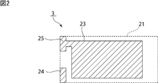
- FIG. 2 is a plan view schematically showing the electrode shape on the lower surface of the piezoelectric vibrator used in the first embodiment.
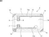
- FIG. 3 is a schematic plan view showing the relationship between the electrode structure on the upper surface of the substrate and the position of the metal cap to be mounted in the first embodiment.
- FIG. 4 is a diagram illustrating a relationship between the frequency when the length of the protruding electrode portion is changed and the electric field strength of the piezoelectric vibrating component in the piezoelectric vibrating component according to the first embodiment.
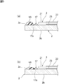
- FIG. 5A and FIG. 5B are schematic cross-sectional views showing the initial state where the sealing adhesive is applied and the state of the adhesive on the substrate during heating.
- FIG. 6A and FIG. 6B are schematic cross-sectional views showing the initial state where the sealing adhesive is applied and the state of the adhesive on the substrate during heating.
- FIG. 1 is an exploded perspective view of a piezoelectric vibration component according to an embodiment of the present invention.
- the piezoelectric vibration component 1 has a rectangular plate-like substrate 2.
- the piezoelectric vibrator 3 is mounted on the upper surface of the substrate 2.
- a cap 5 made of metal is fixed on the upper surface of the substrate 2 so as to surround the mounted piezoelectric vibrator 3. This fixing is performed using a frame-shaped adhesive layer 4.
- the substrate 2 is made of an appropriate insulating material such as insulating ceramics.
- the substrate 2 has a rectangular plate shape.
- the substrate 2 has an upper surface 2a and a lower surface 2b.
- the upper surface 2a has first and second sides 2c and 2d facing each other and third and fourth sides 2e and 2f facing each other.
- the first and second sides 2c and 2d are short sides
- the third and fourth sides 2e and 2f are long sides.
- the short side and the long side may be reversed.
- the first to fourth sides 2c to 2f may have the same length.
- First and second mounting electrodes 6 and 7 are formed on the upper surface 2 a of the substrate 2.
- Conductive adhesives 8 and 9 are applied on the first and second attachment electrodes 6 and 7.
- the conductive adhesives 8 and 9 electrically and mechanically connect the piezoelectric vibrator 3 to the first and second attachment electrodes 6 and 7. That is, the first and second attachment electrodes 6 and 7 also function as a portion that mechanically holds the piezoelectric vibrator 3.
- a corner portion formed by the first side 2c and the third side 2e is defined as a first corner.
- a corner portion formed by the first side 2c and the fourth side 2f is defined as a second corner.
- a corner portion formed by the second side 2d and the third side 2e is defined as a third corner.
- a corner portion formed by the second side 2d and the fourth side 2f is defined as a fourth corner.
- the first attachment electrode 6 is provided closer to the first corner.
- the term “close to the first corner” means that the first to fourth corners are closest to the first corner.
- the second attachment electrode 7 is provided closer to the second corner among the first to fourth corners.
- the first to fourth corners of the substrate 2 are processed so as to have a semicylindrical curved concave portion extending in the vertical direction.
- the first terminal electrode 11 is formed on the inner surface of the recess.
- the second terminal electrode 12 is formed on the inner surface of the recess at the second corner that is diagonal to the third corner.
- the first dummy electrode 13 is formed on the inner surface of the recess.
- a second dummy electrode 14 is formed at the first corner.
- the first and second terminal electrodes 11 and 12 are portions that electrically connect the piezoelectric vibration component 1 to the outside and operate the piezoelectric vibrator 3.
- the first and second dummy electrodes 13 and 14 are connected to the ground potential.
- a first wiring electrode 15 is provided on the upper surface 2 a of the substrate 2.
- the first wiring electrode 15 is provided so as to electrically connect the first attachment electrode 6 and the first terminal electrode 11.
- the first wiring electrode 15 has a linear shape and extends in parallel with the third side 2e.
- the first wiring electrode 15 may be provided non-parallel to the third side 2e.
- the outer edge 15 a of the first wiring electrode 15 is located inside the opening edge of the cap 5.
- the outer edge 15a is a side of the wiring electrode 15 and is an outer side extending in parallel with the third side 2e.
- the second attachment electrode 7 is electrically connected to the second terminal electrode 12 by the second wiring electrode 16.
- the second wiring electrode 16 is provided on the upper surface 2a.
- a protruding electrode portion 17 is provided so as to extend from the second mounting electrode 7 toward the fourth corner.
- the protruding electrode portion 17 has a strip shape having a length direction. More specifically, the protruding electrode portion 17 extends in parallel with the first wiring electrode 15.
- the protruding electrode portion 17 is not limited to a strip shape. Further, it is not necessarily arranged in parallel with the first wiring electrode 15.
- the outer edge 17 a of the protruding electrode portion 17 is located inside the opening edge of the cap 5 after the cap 5 is fixed.
- the outer edge 17a of the protruding electrode portion 17 refers to the side on the fourth side 2f side.
- Each electrode formed on the surface of the substrate 2 including the first and second attachment electrodes 6 and 7 can be formed of an appropriate metal or alloy such as Ag, Cu, or Al.
- the piezoelectric vibrator 3 has a rectangular plate-shaped piezoelectric plate 21.
- the piezoelectric plate 21 is made of a piezoelectric material such as PZT ceramics or quartz.
- a first excitation electrode 22 is formed on the upper surface of the piezoelectric plate 21.
- the first excitation electrode 22 is electrically connected to the first extraction electrode 24.
- the first extraction electrode 24 is provided so as to extend from the upper surface to the lower surface of the piezoelectric plate 21.
- FIG. 2 is a plan view schematically showing the electrode shape on the lower surface of the piezoelectric vibrator 3.
- a second excitation electrode 23 is formed on the lower surface of the piezoelectric plate 21.
- the second excitation electrode 23 is provided so as to overlap with the first excitation electrode 22 via the piezoelectric plate 21.
- the second excitation electrode 23 is electrically connected to the second extraction electrode 25.
- the first and second lead electrodes 24 and 25 are joined to the second attachment electrode 7 and the first attachment electrode 6 shown in FIG. Thereby, the piezoelectric vibrator 3 is held on the substrate 2. That is, the piezoelectric vibrator 3 is mechanically and electrically connected to the first and second attachment electrodes 6 and 7.
- the piezoelectric vibrator used in the present invention is not limited to the piezoelectric vibrator 3, and piezoelectric vibrators excited in various vibration modes can be used. That is, an appropriate piezoelectric vibrator that is joined by the first and second attachment electrodes 6 and 7 and is supported in a cantilever manner can be used.
- a frame-like adhesive layer 4 is provided on the substrate 2.
- the frame-shaped adhesive layer 4 is formed by applying an adhesive in a frame shape and curing it.
- an adhesive mainly composed of a thermosetting resin such as an epoxy resin or a silicon resin can be preferably used.
- an adhesive containing a thermoplastic resin may be used.
- the cap 5 is made of an appropriate metal or alloy such as Cu, Al, or Ni.
- the cap 5 has an opening that opens downward. The opening edge is bonded to the upper surface 2 a of the substrate 2 through the adhesive layer 4.
- the piezoelectric vibrator 3 is enclosed in a package including the substrate 2 and the cap 5. That is, the cap 5 is fixed to the upper surface of the substrate 2 so as to surround the piezoelectric vibrator 3.
- FIG. 3 is a schematic plan view showing the positional relationship between the position where the cap 5 is fixed and the electrode structure on the upper surface 2 a of the substrate 2.
- the cap 5 is fixed at a position indicated by a two-dot chain line on the upper surface 2 a of the substrate 2.
- the cap 5 is mounted and fixed.
- an adhesive may be applied to the cap 5 in advance and then fixed to the upper surface 2a of the substrate 2.
- the outer edge 15a of the first wiring electrode 15 is located inside the region where the cap 5 is provided.
- the outer edge 17 a of the protruding electrode portion 17 is also located inside the opening edge of the cap 5.
- FIG. 4 is a diagram showing the relationship between the frequency and the electric field strength of the signal when the length of the protruding electrode portion 17 is changed to the first length L1, the second length L2, and the third length L3. It is.
- the frequency of the electric field intensity peak of the piezoelectric vibrating component 1 is shifted to the high frequency side.
- the change in the peak of the electric field intensity means that the noise peak frequency changes.
- Higher electric field strength means higher noise resistance. In other words, it is preferable that the electric field strength level is high in order to obtain the required electric field strength regardless of the influence of electromagnetic noise applied from the outside.
- the electric field strength level shown by the broken line S in FIG. 4 be the required electric field strength level. If this required field strength level is S or higher, the influence of noise can be ignored.
- the frequency position of the peak of the electric field strength can be changed by changing the length of the protruding electrode portion 17. Therefore, for example, when the frequency range from F1 to F2 in FIG. 4 is a noise tolerance evaluation range, that is, a range where noise tolerance is required, in order to obtain such noise tolerance, the length of the protruding electrode portion 17 should be adjusted. I understand that That is, for example, it is understood that the protruding electrode portion 17 may be formed so that the second length is L2.
- the present embodiment it is possible to increase the noise tolerance by adjusting the length of the protruding electrode portion 17 in the frequency range where the noise tolerance is required.
- the peak frequency of the electric field strength varies depending on the length of the protruding electrode portion 17 as described above, although it is not necessarily clear. That is, it is considered that the wiring routing state of the entire circuit changes due to a change in the distance between the tip of the protruding electrode portion 17 and the first dummy electrode 13 connected to the ground potential. That is, it is considered that the entire circuit constant is changed and the peak position of the electric field intensity is changed.
- the first dummy electrode 13 is preferably connected to the ground potential as in the present embodiment.
- the first dummy electrode 13 is not necessarily connected to the ground potential. Even in such a case, when the length of the protruding electrode portion 17 is changed, it is confirmed that the peak frequency position of the electric field strength changes as described above, although not as in the case of the present embodiment.
- the piezoelectric vibration component 1 of the present embodiment since the protruding electrode portion 17 is provided, disconnection of electrodes and wiring electrodes in the vibration leakage path portion is unlikely to occur.
- the substrate 2 becomes smaller and thinner. In that case, the substrate 2 may be easily deformed by an external force.
- the wiring electrode portion such as the first wiring electrode 15 may break due to the deformation of the substrate 2.
- the rigidity of the substrate 2 is increased by the amount of the protruding electrode portion 17 provided.
- the rigidity of the substrate 2 is increased by the amount of the protruding electrode portion 17 provided.
- the protruding electrode portion 17 since the protruding electrode portion 17 is provided, the characteristics are hardly deteriorated due to the flow of the adhesive constituting the adhesive layer 4.
- the viscosity of the adhesive decreases. As a result, the adhesive may adhere to the piezoelectric vibrator and deteriorate characteristics.
- an adhesive 4 ⁇ / b> A for forming an adhesive layer is applied on the upper surface 2 a of the substrate 2.
- the outer edge 17a of the protruding electrode part 17 is located inside the opening edge of the cap 5 described above. Therefore, the adhesive 4 ⁇ / b> A is applied to the outside of the protruding electrode portion 17.
- the viscosity of the adhesive 4A decreases and expands as shown in FIG.
- the protruding electrode portion 17 is provided on the inner side, wetting and spreading of the adhesive 4A can be suppressed. Thereby, adhesion of the adhesive 4A to the piezoelectric vibrator 3 side can be reliably prevented.
- the adhesive 4A may be applied so as to reach a part of the upper surface of the protruding electrode portion 17. Even in this case, when heated, the adhesive 4A wets and spreads the upper surface of the protruding electrode portion 17 as shown in FIG. Therefore, adhesion of the adhesive 4A to the piezoelectric vibrator 3 can be surely prevented.
- the protruding electrode portion 17 by providing the protruding electrode portion 17, it is possible to reliably suppress deterioration of characteristics due to adhesion of the adhesive 4 ⁇ / b> A to the piezoelectric vibrator 3.
- the protruding electrode portion 17 has a strip shape, but the protruding electrode portion 17 is not limited to a single linear shape.
- the protruding electrode portion 17 may be divided into a plurality of electrode portions. Further, the protruding electrode portion 17 may have a shape other than a linear shape. Furthermore, the shape provided with the appropriate recessed part and convex part may be sufficient. That is, the shape of the protruding electrode portion 17 is not particularly limited.
Landscapes
- Physics & Mathematics (AREA)
- Acoustics & Sound (AREA)
- Piezo-Electric Or Mechanical Vibrators, Or Delay Or Filter Circuits (AREA)
Abstract
外部からのノイズによる影響を抑制することができる圧電振動部品を提供する。 矩形板状の基板2の上面2a上に、圧電振動子3が保持されており、該圧電振動子3を囲繞するように金属からなるキャップ5が上面2aに固定されており、基板2の上面2aに設けられた第1,第2の取付電極6,7に圧電振動子3が機械的かつ電気的に接続されており、基板2の第2のコーナーに第2の端子電極12が、第3のコーナーに第1の端子電極11が設けられており、第2の取付電極7から第4のコーナー側に向かって突出電極部17が設けられている、圧電振動部品1。
Description
本発明は、基板上に圧電振動子が搭載されている圧電振動部品に関する。
従来、発振子やフィルタとして様々な圧電振動部品が提案されている。下記の特許文献1には、この種の圧電振動部品の一例が開示されている。特許文献1に記載の圧電振動部品では、矩形板状の基板上に圧電振動子が保持されている。矩形板状の基板の上面には、圧電振動子を電気的に接続し、かつ保持するための第1,第2の取付電極が形成されている。基板の1つのコーナーには第1の端子電極が形成されている。この第1の端子電極に第1の取付電極が形成されている。他のコーナーに第2の端子電極が形成されている。第2の端子電極に、配線電極により第2の取付電極が電気的に接続されている。そして、上記圧電振動子を囲繞するように、接着剤を介して基板の上面に金属からなるキャップが固定されている。
特許文献1に記載の圧電振動部品では、外部からの電磁ノイズを受けた場合、金属からなるキャップがアンテナとして動作し、ノイズ耐性が劣化するという問題があることがわかった。
本発明の目的は、外部からのノイズによる影響を抑制することが可能とされている圧電振動部品を提供することにある。
本発明に係る圧電振動部品は、基板と、第1,第2の取付電極と、圧電振動子と、金属からなるキャップとを備える。基板は、上面と下面とを有する。基板は矩形板状の基板であり、上面が、対向し合う第1,第2の辺と、対向し合う第3,第4の辺とを有する。キャップは、上記基板上に搭載された上記圧電振動子を囲繞するように上記基板に固定されており、かつ基板側に開いた開口を有する。
第1,第2の取付電極は、上記基板の上面に形成されている。
圧電振動子は、上記第1,第2の取付電極に電気的かつ機械的に接続されており、基板の上面に保持されている。
上記基板の上面において、第1の辺と第3の辺とがなすコーナー部を第1のコーナー、第1の辺と第4の辺とがなすコーナー部を第2のコーナー、第2の辺と第3の辺とがなすコーナー部を第3のコーナー、第2の辺と第4の辺とがなすコーナー部を第4のコーナーとする。
基板の上面において、上記第1の取付電極が、第1~第4のコーナーのうち、第1のコーナー寄りに設けられている。第2の取付電極は、第1~第4のコーナーのうちの第2のコーナー寄りに設けられている。
本発明に係る圧電振動部品は、さらに、第1,第2の端子電極、第1,第2の配線電極及び突出電極部を備える。第1の端子電極は第3のコーナーに設けられており、第2の端子電極は第2のコーナーに設けられている。第1の配線電極は、第1の取付電極と第1の端子電極とを接続するように基板の上面に設けられている。第2の配線電極は、第2の取付電極と第2の端子電極とを接続するように基板の上面に設けられている。
突出電極部は、第2の取付電極に電気的に接続されるように基板の上面において第2の取付電極から第4のコーナー側に向かって延ばされている。
本発明に係る圧電振動部品では、好ましくは、基板の第4のコーナーに設けられており、かつグラウンド電位に接続される第1のダミー電極がさらに備えられている。
本発明に係る圧電振動部品では、第1のコーナーに設けられた第2のダミー電極がさらに備えられていてもよい。
本発明に係る圧電振動部品では、上記キャップは、基板の上面に接着剤により固定されていてもよい。この場合、好ましくは、突出電極部及び第1の配線電極の外側縁がキャップの開口縁よりも内側に位置している。
本発明に係る圧電振動部品によれば、上記突出電極部が設けられているため、外部からの電磁波ノイズを受けた場合、該突出電極部の長さ及び形状を調整することにより該ノイズの強度のピーク位置にある周波数を制御することができる。従って、電磁波ノイズの影響を受け難い、圧電振動部品を提供することが可能となる。
以下、図面を参照しつつ、本発明の具体的な実施形態を説明することにより、本発明を明らかにする。
図1は、本発明の一実施形態にかかる圧電振動部品の分解斜視図である。
図1に示すように、圧電振動部品1は、矩形板状の基板2を有する。
この基板2の上面に圧電振動子3が搭載されている。搭載されている圧電振動子3を囲繞するように、金属からなるキャップ5が基板2の上面に固定される。この固定は、枠状の接着剤層4を用いて行われる。
基板2は絶縁性セラミックスなどの適宜の絶縁性材料からなる。基板2は矩形板状の形状を有する。基板2は、上面2aと、下面2bとを有する。上面2aは、対向し合う第1,第2の辺2c,2dと、対向し合う第3,第4の辺2e,2fとを有する。本実施形態では、第1,第2の辺2c,2dが短辺であり、第3,第4の辺2e,2fが長辺である。もっとも、短辺と長辺は逆であってもよい。また、第1~第4の辺2c~2fは同じ長さであってもよい。
基板2の上面2a上には、第1,第2の取付電極6,7が形成されている。第1,第2の取付電極6,7上には、導電性接着剤8,9が付与されている。導電性接着剤8,9は、圧電振動子3を第1,第2の取付電極6,7に電気的にかつ機械的に接続している。すなわち、第1,第2の取付電極6,7は、圧電振動子3を機械的に保持する部分としても機能する。
基板2において、第1の辺2cと第3の辺2eとのなすコーナー部を第1のコーナーとする。第1の辺2cと第4の辺2fとのなすコーナー部を第2のコーナーとする。第2の辺2dと第3の辺2eとのなすコーナー部を第3のコーナーとする。第2の辺2dと第4の辺2fとのなすコーナー部を第4のコーナーとする。
上面2a上において、第1の取付電極6は、第1のコーナー寄りに設けられている。第1のコーナー寄りとは、第1~第4のコーナーのうち、第1のコーナーにもっとも近いことを意味する。他方、第2の取付電極7は、第1~第4のコーナーのうち、第2のコーナー寄りに設けられている。
他方、必須ではないが、本実施形態では、基板2の第1~第4のコーナーは、上下方向に延びる半円筒曲面状の凹部を有するように加工されている。第3のコーナーにおいては、この凹部内面に第1の端子電極11が形成されている。第3のコーナーとは対角位置にある第2のコーナーにおいては、凹部内面に第2の端子電極12が形成されている。他方、第4のコーナーにおいては、凹部内面に第1のダミー電極13が形成されている。第1のコーナーには、第2のダミー電極14が形成されている。
第1,第2の端子電極11,12は、圧電振動部品1を外部と電気的に接続し、圧電振動子3を動作させる部分である。他方、第1,第2のダミー電極13,14は、グラウンド電位に接続される。
基板2の上面2a上には、第1の配線電極15が設けられている。第1の配線電極15は、第1の取付電極6と、第1の端子電極11とを電気的に接続するように設けられている。本実施形態では、第1の配線電極15は、直線状の形状を有し、第3の辺2eと平行に延ばされている。なお、第1の配線電極15は、第3の辺2eと非平行に設けられていてもよい。
本実施形態では、上記第1の配線電極15の外縁15aが、キャップ5の開口縁よりも内側に位置している。なお、外縁15aとは、配線電極15の辺であって、第3の辺2eと平行に延びる外側の辺をいうものとする。
他方、第2の取付電極7は、第2の端子電極12に第2の配線電極16により電気的に接続されている。第2の配線電極16は、上面2a上に設けられている。
さらに、第2の取付電極7から、第4のコーナーに向かって延びるように突出電極部17が設けられている。突出電極部17は、本実施形態では、長さ方向を有するストリップ状の形状を有する。より具体的には、突出電極部17は、第1の配線電極15と平行に延びている。突出電極部17は、ストリップ状の形状に限定されるものではない。また、第1の配線電極15と必ずしも平行に配置される必要もない。
突出電極部17の外縁17aは、キャップ5を固定したあとに、キャップ5の開口縁よりも内側に位置している。突出電極部17の外縁17aとは、第4の辺2f側の辺をいうものとする。
上記第1,第2の取付電極6,7を含む基板2の表面に形成される各電極は、Ag、Cu、Alなどの適宜の金属もしくは合金により形成することができる。
圧電振動子3は、矩形板状の圧電板21を有する。圧電板21は、PZT系セラミックスや水晶などの圧電材料からなる。
圧電板21の上面に、第1の励振電極22が形成されている。第1の励振電極22は、第1の引き出し電極24に電気的に接続されている。第1の引き出し電極24は、圧電板21の上面から下面に至るように設けられている。
図2は、圧電振動子3の下面の電極形状を模式的に示す平面図である。圧電板21の下面には、第2の励振電極23が形成されている。第2の励振電極23は、第1の励振電極22と圧電板21を介して重なり合うように設けられている。第2の励振電極23は、第2の引き出し電極25に電気的に接続されている。第1,第2の引き出し電極24,25が図1に示した第2の取付電極7及び第1の取付電極6にそれぞれ導電性接着剤9,8より接合されている。それによって、圧電振動子3が基板2上に保持されている。すなわち、圧電振動子3が第1,第2の取付電極6,7に機械的にかつ電気的に接続されている。
なお、本発明において用いられる圧電振動子については、上記圧電振動子3に限らず、様々な振動モードで励振される圧電振動子を用いることができる。すなわち、第1,第2の取付電極6,7により接合され、片持ちで支持される適宜の圧電振動子を用いることができる。
図1に戻り、基板2上に、枠状の接着剤層4が設けられる。枠状の接着剤層4は、接着剤を枠状に塗布し、硬化させることにより形成される。このような接着剤としては、エポキシ樹脂、シリコン樹脂などの熱硬化性樹脂を主体とする接着剤を好ましく用いることができる。もっとも、熱可塑性樹脂を含む接着剤を用いてもよい。
キャップ5は、Cu、Al、Niなどの適宜の金属もしくは合金からなる。キャップ5は、下方に開いた開口を有する。開口縁が、接着剤層4を介して基板2の上面2aに接合される。それによって、圧電振動子3が、基板2とキャップ5とからなるパッケージ内に囲繞される。すなわち、圧電振動子3を囲繞するようにキャップ5が基板2の上面に固定されている。
図3は、上記キャップ5の固定される位置と基板2の上面2a上の電極構造との位置関係を示す模式的平面図である。図3に示すように、基板2の上面2aにおいて、二点鎖線で示す位置にキャップ5が固定される。言い換えれば、矩形枠状の二点鎖線で示す領域に接着剤を塗布した後、キャップ5を搭載し、固定する。また、あらかじめキャップ5に接着剤を塗布した後に、基板2の上面2aに固定してもよい。
図3から明らかなように、第1の配線電極15の外縁15aは、キャップ5が設けられている領域よりも内側に位置している。同様に、突出電極部17の外縁17aもまた、キャップ5の開口縁よりも内側に位置している。
本実施形態の圧電振動部品1では、突出電極部17が設けられているため、外部からの電磁波ノイズの影響を抑制することが可能とされている。これを、図4を参照して説明する。
図4は、突出電極部17の長さを第1の長さL1、第2の長さL2、第3の長さL3に変化させた場合の周波数と信号の電界強度との関係を示す図である。第1の長さL1<第2の長さL2<第3の長さL3の関係にある。すなわち、第1の長さL1から第3の長さL3に至るにつれて、突出電極部17の長さが長くなっている。
図4から明らかなように、上記突出電極部17の長さを変化させると、圧電振動部品1の電界強度ピークの周波数が高周波数側にシフトすることがわかる。この電界強度のピークが変化することは、ノイズのピーク周波数が変化することを意味する。この電界強度が高いほどノイズ耐性が高いことを意味する。言い換えれば、外部から加わる電磁波ノイズの影響に関わらず、必要な電界強度を得るには、電界強度レベルが高いことが好ましい。
いま、図4における破線Sで示す電界強度レベルを必要電界強度レベルとする。この必要電界強度レベルがS以上の電界強度であれば、ノイズによる影響を無視することができる。
本実施形態では、上記のように、突出電極部17の長さを、変化させることにより、電界強度のピークの周波数位置を変化させることができる。よって、例えば、図4の周波数F1からF2の範囲をノイズ耐性評価範囲、すなわちノイズ耐性が求められる範囲とした場合、このようなノイズ耐性を得るには、突出電極部17の長さを調整すればよいことがわかる。すなわち、例えば、第2の長さをL2となるように突出電極部17を形成すればよいことがわかる。
従って、本実施形態によれば、ノイズ耐性が必要な周波数範囲において、突出電極部17の長さを調整してノイズ耐性を高めることが可能となる。
上記のように電界強度のピーク周波数が突出電極部17の長さにより変化するのは、必ずしも明確ではないが、以下の理由によると考えられる。すなわち、突出電極部17の先端と、グラウンド電位に接続される第1のダミー電極13との間の距離が変化することにより、回路全体の配線の引き回し状態が変化することによると考えられる。すなわち、全体の回路定数が変化し、電界強度のピーク位置が変化しているものと考えられる。
従って、好ましくは、第1のダミー電極13が、本実施形態のようにグラウンド電位に接続されていることが望ましい。もっとも、第1のダミー電極13は必ずしもグラウンド電位に接続されていなくてもよい。その場合であっても、突出電極部17の長さを変化させた場合、上記のように本実施形態の場合程ではないが電界強度のピーク周波数位置は変化することが確かめられている。
さらに、本実施形態の圧電振動部品1では、上記突出電極部17が設けられているため、振動漏洩経路部分における電極や配線電極の断線が生じ難い。圧電振動部品1において小型化を進めた場合、基板2が小さくなり、かつ薄くなる。その場合、外力により基板2が容易に変形するおそれがある。その結果、第1の配線電極15などの配線電極部分において基板2の変形に伴う破断が生じるおそれがある。
これに対して、本実施形態では、突出電極部17が設けられている分だけ、基板2の剛性が高められる。例えば、その長辺方向中央において上下方向に変位するように変形したとしても、第1の配線電極15だけでなく突出電極部17が設けられているため、破断が生じ難い。
加えて、本実施形態では、突出電極部17が設けられているため、接着剤層4を構成する接着剤の流れ出しによる特性の劣化も生じ難い。特許文献1に記載のような圧電振動部品では、接着剤を塗布し、加熱すると、接着剤の粘度が低下する。その結果、接着剤が圧電振動子に付着し、特性を劣化させるおそれがある。
これに対して、本実施形態では、このような接着剤の圧電振動子への付着を確実に抑制することができる。これを図5(a),(b)、図6(a),(b)を参照して説明する。図5(a)に示すように、接着剤層を構成するための接着剤4Aを基板2の上面2a上に塗布する。ここでは、突出電極部17の外縁17aが前述したキャップ5の開口縁よりも内側に位置している。従って、接着剤4Aは突出電極部17の外側に塗布される。加熱すると、図5(b)に示すように、接着剤4Aの粘度が低下して、拡がることとなる。しかしながら、内側には突出電極部17が設けられているため、接着剤4Aの濡れ拡がりを抑制することができる。それによって、圧電振動子3側への接着剤4Aの付着を確実に防止することができる。
また、図6(a)に示すように、接着剤4Aが突出電極部17の上面の一部に至るように塗布されることもある。その場合であっても、加熱した場合、接着剤4Aは、図6(b)に示すように、突出電極部17の上面を濡れ拡がるが、それ以上は内側に濡れ拡がり難い。そのため、接着剤4Aの圧電振動子3への付着をやはり確実に防止することができる。
よって、本実施形態によれば、突出電極部17を設けたことにより、接着剤4Aの圧電振動子3への付着による特性の劣化を確実に抑制することができる。
なお、上記実施形態では、突出電極部17は、ストリップ状の形状を有していたが、突出電極部17は単一の直線状の形状に限定されない。突出電極部17は複数本の電極部分に分割されていてもよい。また、突出電極部17は、直線状の形状以外の形状でもよい。さらに、適宜の凹部や凸部が設けられた形状であってもよい。すなわち、突出電極部17の形状は特に限定されるものではない。
1…圧電振動部品
2…基板
2a…上面
2b…下面
2c…第1の辺
2d…第2の辺
2e…第3の辺
2f…第4の辺
3…圧電振動子
4…接着剤層
4A…接着剤
5…キャップ
6…第1の取付電極
7…第2の取付電極
8,9…導電性接着剤
11…第1の端子電極
12…第2の端子電極
13…第1のダミー電極
14…第2のダミー電極
15…第1の配線電極
15a…外縁
16…第2の配線電極
17…突出電極部
17a…外縁
21…圧電板
22…第1の励振電極
23…第2の励振電極
24…第1の引き出し電極
25…第2の引き出し電極
2…基板
2a…上面
2b…下面
2c…第1の辺
2d…第2の辺
2e…第3の辺
2f…第4の辺
3…圧電振動子
4…接着剤層
4A…接着剤
5…キャップ
6…第1の取付電極
7…第2の取付電極
8,9…導電性接着剤
11…第1の端子電極
12…第2の端子電極
13…第1のダミー電極
14…第2のダミー電極
15…第1の配線電極
15a…外縁
16…第2の配線電極
17…突出電極部
17a…外縁
21…圧電板
22…第1の励振電極
23…第2の励振電極
24…第1の引き出し電極
25…第2の引き出し電極
Claims (5)
- 上面及び下面を有し、上面が対向し合う第1,第2の辺と、対向し合う第3,第4の辺とを有する矩形板状の基板と、
前記基板の前記上面に形成された第1,第2の取付電極と、
前記第1,第2の取付電極に電気的かつ機械的に接続されており、前記基板の上面に保持されている圧電振動子と、
前記基板上に搭載された前記圧電振動子を囲繞するように前記基板に固定されており、かつ基板側に開いた開口を有し、金属からなるキャップとを備え、
前記基板の上面において、前記第1の辺と第3の辺とがなすコーナー部を第1のコーナー、前記第1の辺と第4の辺とがなすコーナー部を第2のコーナー、前記第2の辺と前記第3の辺とがなすコーナー部を第3のコーナー、前記第2の辺と前記第4の辺とがなすコーナー部を第4のコーナーとしたときに、
前記基板の上面において、前記第1の取付電極が第1~第4のコーナーのうち第1のコーナー寄りに設けられており、前記第2の取付電極が前記第1~第4のコーナーのうちの第2のコーナー寄りに設けられており、
前記第3のコーナーに設けられた第1の端子電極と、
前記第2のコーナーに設けられた第2の端子電極と、
前記第1の取付電極と前記第1の端子電極とを接続するように前記基板の上面に設けられている第1の配線電極と、
前記第2の取付電極と前記第2の端子電極とを接続するように前記基板の上面に設けられている第2の配線電極と、
前記第2の取付電極に電気的に接続されるように前記基板の上面において前記第2の取付電極から前記第4のコーナー側に向かって延ばされている突出電極部をさらに備える、圧電振動部品。 - 前記基板の前記第4のコーナーに設けられており、かつグラウンド電位に接続される第1のダミー電極をさらに備える、請求項1に記載の圧電振動部品。
- 前記第1のコーナーに設けられた第2のダミー電極をさらに備える、請求項2に記載の圧電振動部品。
- 前記基板の上面に前記キャップが接着剤により固定されている、請求項1~3のいずれか1項に記載の圧電振動部品。
- 前記突出電極部及び第1の配線電極の外側縁が前記キャップの開口縁よりも内側に位置している、請求項4に記載の圧電振動部品。
Applications Claiming Priority (2)
| Application Number | Priority Date | Filing Date | Title |
|---|---|---|---|
| JP2013009845 | 2013-01-23 | ||
| JP2013-009845 | 2013-01-23 |
Publications (1)
| Publication Number | Publication Date |
|---|---|
| WO2014115451A1 true WO2014115451A1 (ja) | 2014-07-31 |
Family
ID=51227251
Family Applications (1)
| Application Number | Title | Priority Date | Filing Date |
|---|---|---|---|
| PCT/JP2013/084090 Ceased WO2014115451A1 (ja) | 2013-01-23 | 2013-12-19 | 圧電振動部品 |
Country Status (1)
| Country | Link |
|---|---|
| WO (1) | WO2014115451A1 (ja) |
Citations (5)
| Publication number | Priority date | Publication date | Assignee | Title |
|---|---|---|---|---|
| JPH0711028U (ja) * | 1993-07-22 | 1995-02-14 | 株式会社大真空 | 表面実装型圧電振動子 |
| JPH0774581A (ja) * | 1993-08-30 | 1995-03-17 | Daishinku Co | 圧電振動子 |
| JPH10303677A (ja) * | 1997-04-24 | 1998-11-13 | Kyocera Corp | 圧電振動子収納用パッケージ |
| JP2008066912A (ja) * | 2006-09-06 | 2008-03-21 | Daishinku Corp | 圧電振動デバイス |
| WO2009072351A1 (ja) * | 2007-12-06 | 2009-06-11 | Murata Manufacturing Co., Ltd. | 圧電振動部品 |
-
2013
- 2013-12-19 WO PCT/JP2013/084090 patent/WO2014115451A1/ja not_active Ceased
Patent Citations (5)
| Publication number | Priority date | Publication date | Assignee | Title |
|---|---|---|---|---|
| JPH0711028U (ja) * | 1993-07-22 | 1995-02-14 | 株式会社大真空 | 表面実装型圧電振動子 |
| JPH0774581A (ja) * | 1993-08-30 | 1995-03-17 | Daishinku Co | 圧電振動子 |
| JPH10303677A (ja) * | 1997-04-24 | 1998-11-13 | Kyocera Corp | 圧電振動子収納用パッケージ |
| JP2008066912A (ja) * | 2006-09-06 | 2008-03-21 | Daishinku Corp | 圧電振動デバイス |
| WO2009072351A1 (ja) * | 2007-12-06 | 2009-06-11 | Murata Manufacturing Co., Ltd. | 圧電振動部品 |
Similar Documents
| Publication | Publication Date | Title |
|---|---|---|
| JP5884946B2 (ja) | 水晶振動装置 | |
| US8941445B2 (en) | Piezoelectric module | |
| US20090051252A1 (en) | Piezoelectric Resonator Plate And Piezolectric Resonator Device | |
| JP2013251323A (ja) | 電子部品 | |
| JP2009158999A (ja) | 圧電デバイス | |
| JP6233392B2 (ja) | 水晶振動装置及びその製造方法 | |
| WO2018003283A1 (ja) | 弾性波装置及び電子部品 | |
| JP5100408B2 (ja) | 音叉型圧電振動子 | |
| JP3743302B2 (ja) | 電子部品及び電子部品の基板電極形成方法 | |
| KR20010020839A (ko) | 압전 부품 | |
| WO2019131866A1 (ja) | 配線基板、電子装置及び電子モジュール | |
| WO2014115451A1 (ja) | 圧電振動部品 | |
| JP2009272795A (ja) | 圧電振動素子、圧電デバイス、及びその製造方法 | |
| JP2007243535A (ja) | 圧電振動片の接合構造、及び圧電デバイス | |
| JP6457345B2 (ja) | 電子部品搭載用パッケージおよび電子装置 | |
| JP5672928B2 (ja) | 電子部品装置及びその製造方法 | |
| WO2016042972A1 (ja) | 電子部品及び樹脂モールド型電子部品装置 | |
| JP5742623B2 (ja) | 半導体装置 | |
| JP2011054597A (ja) | 電子デバイス | |
| JP6555960B2 (ja) | 電子部品搭載用パッケージおよび電子装置 | |
| JP2007235289A (ja) | 圧電発振器 | |
| JP2010103647A (ja) | 弾性表面波デバイス | |
| JP2008295031A (ja) | 水晶振動デバイス | |
| US20150333729A1 (en) | Piezoelectric package | |
| JP2007096530A (ja) | 圧電振動素子の支持構造、表面実装型圧電振動子、及び表面実装型圧電発振器 |
Legal Events
| Date | Code | Title | Description |
|---|---|---|---|
| 121 | Ep: the epo has been informed by wipo that ep was designated in this application |
Ref document number: 13872952 Country of ref document: EP Kind code of ref document: A1 |
|
| NENP | Non-entry into the national phase |
Ref country code: DE |
|
| 122 | Ep: pct application non-entry in european phase |
Ref document number: 13872952 Country of ref document: EP Kind code of ref document: A1 |
|
| NENP | Non-entry into the national phase |
Ref country code: JP |