WO2014115390A1 - 撮像装置、内視鏡システム及びノイズ除去方法 - Google Patents
撮像装置、内視鏡システム及びノイズ除去方法 Download PDFInfo
- Publication number
- WO2014115390A1 WO2014115390A1 PCT/JP2013/079009 JP2013079009W WO2014115390A1 WO 2014115390 A1 WO2014115390 A1 WO 2014115390A1 JP 2013079009 W JP2013079009 W JP 2013079009W WO 2014115390 A1 WO2014115390 A1 WO 2014115390A1
- Authority
- WO
- WIPO (PCT)
- Prior art keywords
- unit
- signal
- transfer
- transfer line
- reference voltage
- Prior art date
Links
- 238000000034 method Methods 0.000 title claims description 12
- 238000012546 transfer Methods 0.000 claims abstract description 231
- 238000006243 chemical reaction Methods 0.000 claims abstract description 100
- 239000003990 capacitor Substances 0.000 claims abstract description 61
- 230000003287 optical effect Effects 0.000 claims abstract description 9
- 238000003384 imaging method Methods 0.000 claims description 197
- 230000003321 amplification Effects 0.000 claims description 49
- 238000003199 nucleic acid amplification method Methods 0.000 claims description 49
- 230000005540 biological transmission Effects 0.000 claims description 48
- 230000008878 coupling Effects 0.000 claims description 15
- 238000010168 coupling process Methods 0.000 claims description 15
- 238000005859 coupling reaction Methods 0.000 claims description 15
- 238000012545 processing Methods 0.000 description 45
- 238000010586 diagram Methods 0.000 description 26
- 238000005070 sampling Methods 0.000 description 16
- 238000012986 modification Methods 0.000 description 15
- 230000004048 modification Effects 0.000 description 15
- 238000000605 extraction Methods 0.000 description 14
- 230000002596 correlated effect Effects 0.000 description 6
- 230000008859 change Effects 0.000 description 5
- 238000005259 measurement Methods 0.000 description 5
- 230000000875 corresponding effect Effects 0.000 description 4
- 239000000284 extract Substances 0.000 description 4
- 239000011159 matrix material Substances 0.000 description 4
- 230000008569 process Effects 0.000 description 4
- 230000008054 signal transmission Effects 0.000 description 4
- 238000004891 communication Methods 0.000 description 3
- 238000003780 insertion Methods 0.000 description 3
- 230000037431 insertion Effects 0.000 description 3
- 230000000694 effects Effects 0.000 description 2
- 230000008030 elimination Effects 0.000 description 2
- 238000003379 elimination reaction Methods 0.000 description 2
- 238000001727 in vivo Methods 0.000 description 2
- 230000002123 temporal effect Effects 0.000 description 2
- 230000000295 complement effect Effects 0.000 description 1
- 238000012937 correction Methods 0.000 description 1
- 238000013461 design Methods 0.000 description 1
- 238000009792 diffusion process Methods 0.000 description 1
- 238000007667 floating Methods 0.000 description 1
- 230000007274 generation of a signal involved in cell-cell signaling Effects 0.000 description 1
- 238000005286 illumination Methods 0.000 description 1
- 229910044991 metal oxide Inorganic materials 0.000 description 1
- 150000004706 metal oxides Chemical class 0.000 description 1
- 230000000149 penetrating effect Effects 0.000 description 1
- 230000002093 peripheral effect Effects 0.000 description 1
- 239000004065 semiconductor Substances 0.000 description 1
- 238000007493 shaping process Methods 0.000 description 1
- 238000005549 size reduction Methods 0.000 description 1
- 230000000087 stabilizing effect Effects 0.000 description 1
Images


Classifications
-
- A—HUMAN NECESSITIES
- A61—MEDICAL OR VETERINARY SCIENCE; HYGIENE
- A61B—DIAGNOSIS; SURGERY; IDENTIFICATION
- A61B1/00—Instruments for performing medical examinations of the interior of cavities or tubes of the body by visual or photographical inspection, e.g. endoscopes; Illuminating arrangements therefor
- A61B1/00002—Operational features of endoscopes
- A61B1/00011—Operational features of endoscopes characterised by signal transmission
- A61B1/00018—Operational features of endoscopes characterised by signal transmission using electrical cables
-
- A—HUMAN NECESSITIES
- A61—MEDICAL OR VETERINARY SCIENCE; HYGIENE
- A61B—DIAGNOSIS; SURGERY; IDENTIFICATION
- A61B1/00—Instruments for performing medical examinations of the interior of cavities or tubes of the body by visual or photographical inspection, e.g. endoscopes; Illuminating arrangements therefor
- A61B1/00002—Operational features of endoscopes
- A61B1/00004—Operational features of endoscopes characterised by electronic signal processing
- A61B1/00009—Operational features of endoscopes characterised by electronic signal processing of image signals during a use of endoscope
- A61B1/000095—Operational features of endoscopes characterised by electronic signal processing of image signals during a use of endoscope for image enhancement
-
- H—ELECTRICITY
- H04—ELECTRIC COMMUNICATION TECHNIQUE
- H04N—PICTORIAL COMMUNICATION, e.g. TELEVISION
- H04N23/00—Cameras or camera modules comprising electronic image sensors; Control thereof
- H04N23/60—Control of cameras or camera modules
- H04N23/66—Remote control of cameras or camera parts, e.g. by remote control devices
-
- H—ELECTRICITY
- H04—ELECTRIC COMMUNICATION TECHNIQUE
- H04N—PICTORIAL COMMUNICATION, e.g. TELEVISION
- H04N25/00—Circuitry of solid-state image sensors [SSIS]; Control thereof
- H04N25/60—Noise processing, e.g. detecting, correcting, reducing or removing noise
-
- H—ELECTRICITY
- H04—ELECTRIC COMMUNICATION TECHNIQUE
- H04N—PICTORIAL COMMUNICATION, e.g. TELEVISION
- H04N25/00—Circuitry of solid-state image sensors [SSIS]; Control thereof
- H04N25/60—Noise processing, e.g. detecting, correcting, reducing or removing noise
- H04N25/616—Noise processing, e.g. detecting, correcting, reducing or removing noise involving a correlated sampling function, e.g. correlated double sampling [CDS] or triple sampling
-
- H—ELECTRICITY
- H04—ELECTRIC COMMUNICATION TECHNIQUE
- H04N—PICTORIAL COMMUNICATION, e.g. TELEVISION
- H04N25/00—Circuitry of solid-state image sensors [SSIS]; Control thereof
- H04N25/60—Noise processing, e.g. detecting, correcting, reducing or removing noise
- H04N25/63—Noise processing, e.g. detecting, correcting, reducing or removing noise applied to dark current
-
- H—ELECTRICITY
- H04—ELECTRIC COMMUNICATION TECHNIQUE
- H04N—PICTORIAL COMMUNICATION, e.g. TELEVISION
- H04N25/00—Circuitry of solid-state image sensors [SSIS]; Control thereof
- H04N25/60—Noise processing, e.g. detecting, correcting, reducing or removing noise
- H04N25/65—Noise processing, e.g. detecting, correcting, reducing or removing noise applied to reset noise, e.g. KTC noise related to CMOS structures by techniques other than CDS
-
- H—ELECTRICITY
- H04—ELECTRIC COMMUNICATION TECHNIQUE
- H04N—PICTORIAL COMMUNICATION, e.g. TELEVISION
- H04N25/00—Circuitry of solid-state image sensors [SSIS]; Control thereof
- H04N25/70—SSIS architectures; Circuits associated therewith
- H04N25/709—Circuitry for control of the power supply
-
- H—ELECTRICITY
- H04—ELECTRIC COMMUNICATION TECHNIQUE
- H04N—PICTORIAL COMMUNICATION, e.g. TELEVISION
- H04N25/00—Circuitry of solid-state image sensors [SSIS]; Control thereof
- H04N25/70—SSIS architectures; Circuits associated therewith
- H04N25/71—Charge-coupled device [CCD] sensors; Charge-transfer registers specially adapted for CCD sensors
- H04N25/75—Circuitry for providing, modifying or processing image signals from the pixel array
-
- H—ELECTRICITY
- H04—ELECTRIC COMMUNICATION TECHNIQUE
- H04N—PICTORIAL COMMUNICATION, e.g. TELEVISION
- H04N25/00—Circuitry of solid-state image sensors [SSIS]; Control thereof
- H04N25/70—SSIS architectures; Circuits associated therewith
- H04N25/76—Addressed sensors, e.g. MOS or CMOS sensors
-
- H—ELECTRICITY
- H04—ELECTRIC COMMUNICATION TECHNIQUE
- H04N—PICTORIAL COMMUNICATION, e.g. TELEVISION
- H04N25/00—Circuitry of solid-state image sensors [SSIS]; Control thereof
- H04N25/70—SSIS architectures; Circuits associated therewith
- H04N25/76—Addressed sensors, e.g. MOS or CMOS sensors
- H04N25/766—Addressed sensors, e.g. MOS or CMOS sensors comprising control or output lines used for a plurality of functions, e.g. for pixel output, driving, reset or power
-
- H—ELECTRICITY
- H01—ELECTRIC ELEMENTS
- H01L—SEMICONDUCTOR DEVICES NOT COVERED BY CLASS H10
- H01L27/00—Devices consisting of a plurality of semiconductor or other solid-state components formed in or on a common substrate
- H01L27/14—Devices consisting of a plurality of semiconductor or other solid-state components formed in or on a common substrate including semiconductor components sensitive to infrared radiation, light, electromagnetic radiation of shorter wavelength or corpuscular radiation and specially adapted either for the conversion of the energy of such radiation into electrical energy or for the control of electrical energy by such radiation
- H01L27/144—Devices controlled by radiation
- H01L27/146—Imager structures
- H01L27/14643—Photodiode arrays; MOS imagers
-
- H—ELECTRICITY
- H04—ELECTRIC COMMUNICATION TECHNIQUE
- H04N—PICTORIAL COMMUNICATION, e.g. TELEVISION
- H04N23/00—Cameras or camera modules comprising electronic image sensors; Control thereof
- H04N23/50—Constructional details
- H04N23/555—Constructional details for picking-up images in sites, inaccessible due to their dimensions or hazardous conditions, e.g. endoscopes or borescopes
Definitions
- the present invention relates to an imaging apparatus, an endoscope system including the imaging apparatus, and a noise removal method including the imaging apparatus.
- CMOS Complementary Metal-Oxide Semiconductor
- FIG. 15 is a circuit diagram showing a configuration of a conventional imaging apparatus.
- the imaging apparatus 500 includes a CMOS image sensor will be described.
- the imaging apparatus 500 is disposed, for example, at the distal end portion of the endoscope, and includes a light receiving unit and a reading unit.
- the light receiving unit includes a plurality of unit pixels 530 arranged in a two-dimensional matrix over a plurality of rows and columns, and a vertical transfer line 539 for transferring a signal output from each unit pixel 530.
- the reading unit includes a vertical scanning unit (row selection circuit) 541, a noise removing unit 543 provided for each pixel column, and a horizontal scanning unit (column selection circuit) 558.
- Each unit pixel 530 includes a photodiode that accumulates signal charges according to the amount of incident light, a charge conversion unit that converts signal charges transferred from the photodiodes, and a transfer that transfers signal charges from the photodiodes to the charge conversion unit.
- the transistor, the reset transistor that resets the signal charge transferred to the charge converter, the row selection transistor, and the row selection transistor are in the on state, the voltage level change of the voltage-converted signal charge is handled by the source follower
- the vertical transfer line 539 includes an output transistor that outputs an image pickup signal.
- the reading unit turns on the row selection transistor of an arbitrary row by the vertical scanning unit (row selection circuit) 541 and reads the imaging signal to the vertical transfer line 539.
- the read imaging signal is input to the noise removing unit 543, and the noise component is removed. Thereafter, the image data is output to the outside by the horizontal scanning unit 558 as image information.
- FIG. 16 is a circuit diagram showing the configuration of the noise removal unit of the imaging apparatus shown in FIG.
- the noise removing unit 543 includes a sample and hold transistor 544 having one end connected to the vertical transfer line 539, a coupling capacitor (AC coupling capacitor) CC having one end connected to the other end of the transistor 544, and an AC coupling capacitor CC.
- a charge storage capacitor (sample capacitor) CS connected between the other end of the capacitor and ground, and a potential clamping transistor 545 connected to a connection node SN between the AC coupling capacitor CC and the sample capacitor CS.
- the connection node SN is connected to the horizontal scanning unit 558.
- the noise removing unit 543 first turns on the sample and hold transistor 544 at the time of pixel reset, transmits the noise signal transferred by the vertical transfer line 539 through the AC coupling capacitor CC, and sets the potential clamping transistor 545 to a predetermined value.
- the noise signal level is sampled in the sample capacitor CS while being turned on for a period. Thereafter, when the imaging signal is read out, the imaging signal including the noise signal (optical noise sum signal) is transmitted again by the AC coupling capacitor CC. Since the voltage change of the imaging signal after pixel reset is transmitted, as a result, the imaging signal obtained by subtracting the noise signal from the optical noise sum signal can be extracted.
- the noise removing unit 543 shown in FIG. 16 requires two capacitors, an AC coupling capacitor CC and a sample capacitor CS, for each pixel column.
- the size of the capacitor becomes a restriction, and it is difficult to reduce the size of the imaging device.
- the gain is reduced and the S / N ratio is deteriorated due to the capacitive division of the AC coupling capacitor CC and the sample capacitor CS.
- it is necessary to increase the AC coupling capacitance CC, which makes it more difficult to reduce the size.
- the endoscope is provided with an imaging device at the distal end portion, and the imaging device at the distal end portion and a control device such as a processor are connected via a transmission cable of several meters. Therefore, when using an imaging apparatus for an endoscope, an imaging signal must be transmitted over a long distance via a transmission cable, and there is a high possibility that noise will be mixed during transmission. However, if only the imaging signal is transmitted from the imaging device, it is difficult to remove noise mixed in during transmission.
- the present invention has been made in view of the above, and an object of the present invention is to provide an imaging apparatus, an endoscope system, and a noise removal method in which image quality does not deteriorate while achieving miniaturization.
- an imaging apparatus performs photoelectric conversion according to the amount of received light, and stores a photoelectric conversion element that accumulates charges and a first charge that transfers the accumulated charges.
- a transfer unit that converts the transferred charge into a voltage or current signal, a charge conversion unit reset unit that resets the charge conversion unit to a first voltage, and outputs the converted signal
- a signal output unit a first transfer line connected to the signal output unit, a transfer capacitor connected to the first transfer line, and the first transfer line via the transfer capacitor;
- a second transfer unit that outputs a signal from the first transfer line, a transfer capacitor reset unit that resets the transfer capacitor to a second voltage, and a second transfer by coupling by the capacity of the transfer capacitor
- the second switch that outputs the signal from the The line and the first transfer unit are turned off, and the charge conversion unit is reset by the charge conversion unit reset unit, and then the signal of the charge conversion unit is transferred to the first transfer unit via the signal output unit.
- a noise signal readout operation for resetting the transfer capacitor by the transfer capacitor reset unit when outputting to a line; and turning off the transfer capacitor reset unit and turning on the first transfer unit to perform the photoelectric conversion After transferring the charge accumulated in the element, an optical noise sum signal reading operation for outputting the signal of the charge conversion unit to the first transfer line via the signal output unit from the first transfer line. And a drive unit that outputs a signal via the second transfer unit.
- a reference voltage generation unit that generates a reference voltage having a fluctuation component in phase with the second voltage, the second transfer line, and the reference voltage generation unit And an output selection unit that selects and outputs the signal input from the second transfer line and the reference voltage input from the reference voltage generation unit.
- the imaging device is the above-described invention, further comprising: a second transfer line reset unit that resets the second transfer line to a third voltage; and the second transfer line and the output selection unit.
- a sample hold unit provided between the first transfer line and the first transfer line when the signal of the first transfer line is output to the second transfer line. After the signal output from the line is sampled, only the signal output from the first transfer line is input to the output selection unit by repeatedly resetting the second transfer line. To do.
- the imaging apparatus further includes a reference voltage generation unit that generates a reference voltage based on the first voltage in the above invention, and the reference voltage generation unit converts the voltage of the reference voltage generation unit into the first voltage.
- a reference voltage generation unit reset unit that resets to a voltage of 1, a reference voltage generation unit signal output unit that outputs a signal of the reference voltage generation unit reset unit, and a signal from the reference voltage generation unit signal output unit,
- a third transfer unit that outputs the second transfer line as a voltage to the second transfer line, and the drive unit alternately outputs a signal output from the first transfer line and the reference voltage to the second transfer line.
- the second transfer unit and the third transfer unit are driven so as to be output to a line.
- An endoscope system includes: the imaging device according to the invention described above; a transmission unit that transmits a signal output from the first transfer line output from the imaging device and the reference voltage; and the transmission unit It is provided with the receiving part which receives the signal to transmit, and the calculating part which calculates the signal which the said receiving part receives.
- the endoscope system according to the present invention is the endoscope system according to the above invention, wherein the arithmetic unit is configured to measure a signal strength of a signal received by the receiving unit, and the receiving unit based on the measured signal strength. Based on the amplification factor setting unit that sets the amplification factor of the received signal, the amplification factor, and the reference voltage, the signal output from the first transfer line and the reference voltage are calculated, and the first voltage is calculated. And an imaging signal calculation unit that outputs an imaging signal obtained by subtracting the in-phase noise component at the time of transmission from the signal output from the transfer line.
- the imaging signal calculation unit is based on a DC component extraction unit that extracts a DC component of the reference voltage, the amplification factor, and the DC component.
- a noise component removing unit that removes an in-phase noise component at the time of transmission included in a signal output from one transfer line.
- a photoelectric conversion element that performs photoelectric conversion according to the amount of received light and accumulates charges, a first transfer unit that transfers the accumulated charges, and the transferred charges as a voltage
- the charge converter is connected to the current signal; the charge converter is reset to the first voltage; the signal output unit that outputs the converted signal; and the signal output unit.
- a second transfer unit that outputs a signal from the transfer line, a transfer capacitance reset unit that resets the transfer capacitor to a second voltage, and a second transfer that outputs a signal from the second transfer unit And noise in an imaging device comprising
- the first transfer unit is turned off, the charge conversion unit reset unit resets the charge conversion unit, and the signal of the charge conversion unit is transmitted via the signal output unit.
- an image pickup apparatus an endoscope system, and a noise removal method in which image quality does not deteriorate while achieving size reduction.
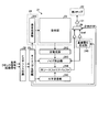
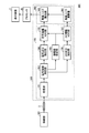
- FIG. 1 is a diagram schematically showing an overall configuration of an endoscope system according to Embodiment 1 of the present invention.
- FIG. 2 is a block diagram showing functions of main parts of the endoscope system according to the first embodiment of the present invention.
- FIG. 3 is a block diagram showing details of the first chip shown in FIG.
- FIG. 4 is a circuit diagram showing a configuration of the first chip of the endoscope system according to the first embodiment.
- FIG. 5 is a circuit diagram illustrating a configuration of a reference voltage generation unit of the endoscope system according to the first embodiment.
- FIG. 6 is a timing chart showing drive signals of the imaging apparatus according to the first embodiment.
- FIG. 7 is a circuit diagram showing a configuration of the first chip of the endoscope system according to the modification of the first embodiment.
- FIG. 1 is a diagram schematically showing an overall configuration of an endoscope system according to Embodiment 1 of the present invention.
- FIG. 2 is a block diagram showing functions of main parts of the endo
- FIG. 8 is a circuit diagram illustrating a configuration of a reference voltage generation unit of the endoscope system according to the modification of the first embodiment.
- FIG. 9 is a timing chart showing drive signals of the imaging apparatus according to the modification of the first embodiment.
- FIG. 10 is a block diagram illustrating functions of the endoscope system according to the second embodiment.
- FIG. 11 is a conceptual diagram for explaining in-phase noise components during transmission in the second embodiment.
- FIG. 12 is a graph for explaining the transmission noise elimination effect according to the second embodiment.
- FIG. 13 is a block diagram illustrating functions of the endoscope system according to the third embodiment.
- FIG. 14 is a conceptual diagram for explaining common-mode noise components during transmission in the third embodiment.
- FIG. 15 is a circuit diagram illustrating a configuration of a conventional imaging device.
- 16 is a circuit diagram illustrating a configuration of a noise removal unit of the imaging apparatus illustrated in FIG.
- an endoscope system including an imaging device will be described as a mode for carrying out the present invention (hereinafter referred to as “embodiment”). Moreover, this invention is not limited by this embodiment. Furthermore, the same code
- FIG. 1 is a diagram schematically showing an overall configuration of an endoscope system according to Embodiment 1 of the present invention.
- An endoscope system 1 shown in FIG. 1 includes an endoscope 2, a transmission cable 3, a connector unit 5, a processor (control device) 6, a display device 7, and a light source device 8.
- the endoscope 2 captures an in-vivo image of the subject by inserting a distal end portion into the body cavity of the subject and outputs an imaging signal.
- the transmission cable 3 connects the endoscope 2 and the connector unit 5.
- the connector unit 5 is connected to the endoscope 2, the processor 6, and the light source device 8, performs predetermined signal processing on the imaging signal output from the connected endoscope 2, and converts the imaging signal into analog / digital (A / D conversion) and output as an image signal.
- the processor 6 performs predetermined image processing on the image signal output from the connector unit 5 and controls the entire endoscope system 1.
- the display device 7 displays the image signal processed by the processor 6.
- the light source device 8 is configured using, for example, a white LED. The pulsed white light that is turned on by the light source device 8 reaches the distal end portion of the insertion portion of the endoscope 2 via the connector portion 5 and the transmission cable 3, and the illumination light that is emitted toward the subject from the distal end portion. Become.
- the endoscope 2 is provided with an imaging unit (imaging device) 20 that captures an in-vivo image on the distal end side of the insertion unit that is inserted into the body cavity of the subject, and the endoscope is provided on the proximal side of the insertion unit.
- An operation unit 4 that receives various operations on 2 is connected.
- the imaging unit 20 is connected to the connector unit 5 via the operation unit 4 by the transmission cable 3.
- the imaging signal of the image captured by the imaging unit 20 is output to the connector unit 5 through the transmission cable 3 having a length of several meters, for example.
- FIG. 2 is a block diagram showing functions of main parts of the endoscope system according to the first embodiment of the present invention. With reference to FIG. 2, the detail of each structure of the endoscope system 1 and the path
- the imaging unit 20 includes a first chip 21 having a light receiving unit 23 and a second chip 22 having a buffer 27.
- the first chip 21 and the second chip 22 are bonded to each other, and the chips are connected by pads disposed on the peripheral edge of the chips, vias penetrating the chips, or the like.
- the first chip 21 and the second chip 22 are not limited to be arranged so that both main surfaces are parallel to each other, but may be arranged side by side or may be arranged side by side with respect to one main surface. It may be arranged so that the main surface of the is vertical.
- the first chip 21 of the imaging unit 20 includes a light receiving unit 23 in which a large number of unit pixels are arranged in a two-dimensional matrix in the matrix direction, a reading unit 24 that reads an imaging signal photoelectrically converted by the light receiving unit 23, and a connector unit.
- 5 includes a timing generation unit 25 that generates a timing signal based on the reference clock signal and the synchronization signal transmitted from 5 and supplies the timing signal to the reading unit 24, and a multiplexer 26 that outputs the imaging signal to the second chip 22.
- the second chip 22 of the imaging unit 20 includes a buffer 27 that functions as a transmission unit that transmits only the AC component of the imaging signal output from the first chip 21 to the processor 6 via the transmission cable 3 and the connector unit 5. .
- the combination of the circuits mounted on the first chip 21 and the second chip 22 can be changed as appropriate according to the design convenience.
- the imaging unit 20 receives the power supply voltage (VDD) generated by the power supply unit 61 in the processor 6 through the transmission cable 3 together with the ground (GND).
- a power supply stabilizing capacitor C1 is provided between the power supply voltage (VDD) supplied to the imaging unit 20 and the ground (GND).
- the connector unit 5 includes an analog front end (AFE) unit 51 and an imaging signal processing unit 52.
- the connector unit 5 functions as a relay processing unit that electrically connects the endoscope 2 (imaging unit 20) and the processor 6 and relays an electrical signal.
- the connector unit 5 and the imaging unit 20 are connected by a transmission cable 3, and the connector unit 5 and the processor 6 are connected by, for example, a coil cable.
- the connector unit 5 is also connected to the light source device 8.
- the AFE unit 51 receives the imaging signal transmitted from the imaging unit 20, performs impedance matching with a passive element such as a resistor, extracts an AC component with a capacitor, and determines an operating point with a voltage dividing resistor. Thereafter, the AFE unit 51 performs analog-to-digital (A / D) conversion on the analog imaging signal and sends the analog imaging signal to the imaging signal processing unit 52 as a digital imaging signal.
- a passive element such as a resistor
- a / D analog-to-digital
- the imaging signal processing unit 52 is configured by, for example, an FPGA (Field Programmable Gate Array), a reference clock signal (for example, a 27 MHz clock) serving as a reference for the operation of each component of the endoscope 2, and a start position of each frame Is generated and supplied to the timing generation unit 25, and predetermined signal processing such as noise removal is performed on the digital imaging signal input from the AFE unit 51.
- FPGA Field Programmable Gate Array
- reference clock signal for example, a 27 MHz clock
- the processor 6 includes a power supply unit 61 and an image signal processing unit 62, and is a control device that controls the entire endoscope system 1.
- the power supply unit 61 generates a power supply voltage (VDD), and supplies the generated power supply voltage to the imaging unit 20 via the connector unit 5 and the transmission cable 3 together with the ground (GND).
- the image signal processing unit 62 performs predetermined image processing on the digital imaging signal that has been subjected to signal processing such as noise removal in the imaging signal processing unit 52, and outputs the image signal to the display device 7.
- the display device 7 displays an image captured by the imaging unit 20 based on the image signal.
- the image processing in the image signal processing unit 62 includes, for example, synchronization processing, white balance (WB) adjustment processing, gain adjustment processing, gamma correction processing, digital analog (D / A) conversion processing, format conversion processing, and the like.
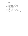
- FIG. 3 is a block diagram showing a detailed configuration of the first chip shown in FIG.
- FIG. 4 is a circuit diagram showing a configuration of the first chip of the endoscope system according to the first embodiment.
- a light receiving unit 23 for example, a light receiving unit 23, a reading unit (drive unit) 24, a timing generation unit 25, and a multiplexer 26 are mounted. Details of the light receiving unit 23 will be described later with reference to FIG.
- a hysteresis circuit 28 is provided before the timing generation unit 25, that is, between the input of the timing generation unit 25 and the processor 6.
- the hysteresis circuit 28 shapes the waveform of the reference clock signal and the synchronization signal transmitted over a long distance by the transmission cable 3.
- the reference clock signal and the synchronization signal that have been subjected to waveform shaping by the hysteresis circuit 28 are input to the timing generator 25.
- the timing generator 25 generates various drive signals ( ⁇ Ta, ⁇ Tb, ⁇ R, ⁇ X, ⁇ VCL, ⁇ HCLR, ⁇ HCLK, ⁇ MUXSEL, ⁇ VSH) based on the reference clock signal and the synchronization signal shaped by the hysteresis circuit 28, and performs vertical scanning. 241, noise removal unit 243, horizontal scanning unit 245, multiplexer 26, and reference voltage generation unit 246.
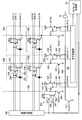
- the reading unit 24 includes a vertical scanning unit (row selection circuit) 241, a constant current source 242, a noise removal unit 243, a column source follower buffer (transistor) 244, a horizontal scanning unit (column selection circuit) 245, a reference Voltage generator 246.
- the noise removing unit 243 removes the output variation for each unit pixel 230 and the noise signal at the time of pixel reset, and outputs the imaging signal photoelectrically converted by each unit pixel 230 to the column source follower buffer 244. Details of the noise removing unit 243 will be described later with reference to FIG.
- the column selection pulse ⁇ HCLK ⁇ M> is applied to the pixel signal, and the imaging signal photoelectrically converted by each unit pixel 230 is transferred to the horizontal transfer line 258 via the column source follower buffer 244 and output to the multiplexer 26.
- the multiplexer 26 is driven by the drive signal ( ⁇ MUXSEL) supplied from the timing generation unit 25, the imaging signal input through the horizontal transfer line 258, and the reference voltage Vref (constant voltage signal) generated by the reference voltage generation unit 246. Are alternately output to the second chip 22 via the output unit (amplifier) 31.
- the reference voltage Vref output here is used in the imaging signal processing unit 52 of the connector unit 5 or the like to remove common-mode noise superimposed on the transmission cable 3 during imaging signal transmission. Note that an amplifier for gain adjustment may be provided on the input side of the multiplexer 26 as necessary.
- Each unit pixel 230 includes photoelectric conversion elements (photodiodes) 231 and 232, a charge conversion unit 233, transfer transistors (first transfer units) 234 and 235, a charge conversion unit reset unit (transistor) 236, pixels A source follower transistor 237 and a pixel output switch (signal output unit) 238.
- photoelectric conversion elements photodiodes
- charge conversion unit 233 transfer transistors
- transfer transistors first transfer units
- transistor charge conversion unit reset unit
- pixels A source follower transistor 237
- a pixel output switch signal output unit
- the photoelectric conversion elements 231 and 232 photoelectrically convert incident light into a signal charge amount corresponding to the amount of the incident light, and accumulate it.
- the cathode sides of the photoelectric conversion elements 231 and 232 are connected to one end sides of the transfer transistors 234 and 235, respectively, and the anode side is connected to the ground GND.
- the charge conversion unit 233 includes a floating diffusion capacitor (FD), and converts charges accumulated in the photoelectric conversion elements 231 and 232 into a voltage.
- FD floating diffusion capacitor
- the transfer transistors 234 and 235 transfer charges from the photoelectric conversion elements 231 and 232 to the charge conversion unit 233, respectively.
- Signal lines to which drive pulses (row selection pulses) ⁇ Ta and ⁇ Tb are supplied are connected to the gates of the transfer transistors 234 and 235, and the other end side is connected to the charge conversion unit 233.
- the transfer transistors 234 and 235 are turned on, and the signal charges are transferred from the photoelectric conversion elements 231 and 232 to the charge conversion unit 233.
- the charge conversion unit reset unit (transistor) 236 resets the charge conversion unit 233 to a predetermined potential.
- the charge conversion unit reset unit 236 has one end connected to the power supply voltage VDD, the other end connected to the charge conversion unit 233, and a gate connected to a signal line to which a drive pulse ⁇ R is supplied.
- ⁇ R is supplied from the vertical scanning unit 241 via the signal line
- the charge conversion unit reset unit 236 is turned on, the signal charge accumulated in the charge conversion unit 233 is released, and the charge conversion unit 233 has a predetermined potential. Reset to.
- the pixel source follower transistor 237 has one end connected to the power supply voltage VDD and the other end connected to one end of the pixel output switch 238.
- a signal (an imaging signal or a reset signal) that has been voltage-converted by the charge conversion unit 233 is input to the gate.
- the pixel output switch 238 outputs the signal voltage-converted by the charge conversion unit 233 to the vertical transfer line 239.
- the other end of the pixel output switch 238 is connected to a vertical transfer line 239, and a signal line to which a drive pulse ⁇ X is supplied is connected to the gate.
- the drive pulse ⁇ X is supplied from the vertical scanning unit 241 to the gate of the pixel output switch 238 via the signal line, the pixel output switch 238 is turned on, and the imaging signal or the reset signal is transferred to the vertical transfer line 239.
- the constant current source 242 has one end connected to the vertical transfer line 239, the other end connected to the ground GND, and a bias voltage Vbias1 applied to the gate.
- the unit pixel 230 is driven by the constant current source 242 and the output of the unit pixel 230 is read to the vertical transfer line 239.
- the signal read to the vertical transfer line 239 is input to the noise removing unit 243.
- the noise removing unit 243 includes a transfer capacitor (AC coupling capacitor) 252 and a clamp switch (transistor) 253.
- the transfer capacitor 252 has one end connected to the vertical transfer line 239 and the other end connected to the column source follower transistor 244.
- One end of the clamp switch 253 is connected to a signal line to which the clamp voltage Vclp is supplied from the reference voltage generation unit 246.
- the other end side of the clamp switch 253 is connected between the transfer capacitor 252 and the column source follower transistor 244, and the drive signal ⁇ VCL is input from the timing generation unit 25 to the gate.
- the imaging signal input to the noise removing unit 243 is an optical noise sum signal including a noise component.
- the clamp switch 253 When the drive signal ⁇ VCL is input from the timing generation unit 25 to the gate of the clamp switch 253, the clamp switch 253 is turned on, and the transfer capacitor 252 is reset by the clamp voltage Vclp supplied from the reference voltage generation unit 246. .
- the imaging signal from which noise has been removed by the noise removing unit 243 is input to the gate of the column source follower transistor 244.
- the noise removing unit 243 does not require a sampling capacitor (sampling capacity)
- the capacity of the transfer capacity (AC coupling capacitor) 252 may be sufficient with respect to the input capacity of the column source follower transistor 244.
- the noise removing unit 243 can reduce the area occupied by the first chip 21 because of the absence of the sampling capacity.
- One end side of the column source follower transistor 244 is connected to the power supply voltage VDD, the other end side is connected to one end side of the column selection switch (second transfer unit) 254, and noise is removed from the gate by the noise removing unit 243.
- the captured image signal is input.
- One end side of the column selection switch 254 is connected to the other end side of the column source follower transistor 244, and the other end side is connected to a horizontal transfer line (second transfer line) 258.
- a signal line for supplying a drive signal ⁇ HCLK ⁇ M> from the horizontal scanning unit 245 is connected to the gate of the column selection switch 254.
- the column selection switch 254 When the driving signal ⁇ HCLK ⁇ M> is supplied from the horizontal scanning unit 245 to the gate of the column selection switch 254 of the column ⁇ M>, the column selection switch 254 is turned on, and the signal of the vertical transfer line 239 of the column ⁇ M> ( The imaging signal from which noise has been removed by the noise removing unit 243) is transferred to the horizontal transfer line 258.
- the constant current source 257 has one end connected to the horizontal transfer line 258, the other end connected to the ground GND, and a bias voltage Vbias2 applied to the gate.
- the constant current source 257 reads the imaging signal from the vertical transfer line 239 to the horizontal transfer line 258.
- the signal read to the horizontal transfer line 258 is input to the sample hold unit 255.
- the horizontal reset transistor 256 One end of the horizontal reset transistor 256 is connected to the horizontal reset voltage Vclr, and the other end is connected to the horizontal transfer line 258.
- the drive signal ⁇ HCLR is input from the timing generation unit 25 to the gate of the horizontal reset transistor 256.
- the horizontal reset transistor 256 is turned on and the horizontal transfer line 258 is reset.
- the sample hold unit 255 includes a buffer 261, a sample hold switch (transistor) 262, a sample capacitance (capacitor) 263, and an operational amplifier 264.
- a horizontal transfer line 258 is connected to the input of the buffer 261, and an imaging signal and a noise signal at the time of horizontal reset are input to the buffer 261 via the horizontal transfer line 258.
- the output of the buffer 261 is connected to one end side of the sample hold switch 262.
- the other end of the sample hold switch 262 is connected to the input of the operational amplifier 264.
- One end of the sample capacitor 263 is connected to the other end of the sample hold switch 262 and the input of the operational amplifier 264, and the other end is connected to the ground GND.
- the output of the operational amplifier 264 is connected to the inverting input terminal of the operational amplifier 264 and to the input of the multiplexer 26.
- the sample hold unit 255 holds the voltage immediately before the sample hold switch 262 is turned off in the sample capacitor 263, and outputs the voltage held in the sample capacitor 263 while the sample hold switch 262 is turned off. .
- the readout of the imaging signal after noise removal from the vertical transfer line 239 and the reset of the horizontal transfer line 258 by the horizontal reset transistor 256 are alternately performed, thereby cross-talking the imaging signal in the column direction. It becomes possible to suppress.
- the sample hold switch 262 of the sample hold unit 255 is turned on when the imaging signal after noise removal is transferred and turned off when the noise signal is transferred after reset, so that only the imaging signal after noise removal is operated by the operational amplifier. H.264 can be output. Since the first chip 21 includes the sample hold unit 255, it is possible to halve the band of the subsequent amplifier circuit and to suppress the range.
- the multiplexer 26 alternately outputs the noise-removed imaging signal output from the sample hold unit 255 and the reference voltage Vref generated by the reference voltage generation unit 246 to the output unit 31.
- the output unit 31 amplifies the image signal from which noise has been removed and the reference voltage Vref as necessary, and alternately outputs the amplified signal to the second chip 22.
- FIG. 5 is a circuit diagram showing a configuration of a reference voltage generation unit of the light receiving unit of the endoscope system according to the first embodiment.
- the reference voltage generation unit (constant voltage signal generation unit) 246 has a resistance voltage dividing circuit made up of two resistors 291 and 292, a switch (transistor) 293 driven by the drive signal ⁇ VSH, and a power supply, and is free from fluctuations. And a sampling capacitor (capacitor) 294 for opening.
- the reference voltage generation unit 246 generates the reference voltage Vref (constant voltage signal) from the same power supply voltage VDD as that of the light receiving unit 23 and the clamp voltage Vclp of the noise removal unit 243 at the timing when the drive signal ⁇ VSH is driven by driving the switch 293. Generate.
- the reference voltage Vref reflects the influence of power supply fluctuation on the imaging signal output from the noise removal unit 243.
- the reference voltage Vref reflects transmission noise information in the transmission cable 3 during transmission. Therefore, by transmitting the noise-removed imaging signal and the reference voltage Vref to the connector unit 5 alternately, the connector unit 5 performs noise removal processing such as correlated double sampling, and removes noise during transmission. A signal can be obtained.
- FIG. 6 is a timing chart showing drive signals of the imaging apparatus according to the first embodiment. In this example, a process from reading a signal from the unit pixel 230 in the row ⁇ n> of the light receiving unit 23 to outputting from the output unit 31 will be described.
- the clamp switch 253 is turned on ( ⁇ VCL is High), the pixel output switch 238 is turned on ( ⁇ X ⁇ n> is High), and the charge conversion unit reset unit 236 is turned on in a pulse shape (the drive pulse ⁇ R ⁇ n> is High).
- the transfer transistors 234 and 235 the drive pulses ⁇ Ta ⁇ n> and ⁇ Tb ⁇ n> are Low
- noise signals including variations peculiar to the unit pixel 230 to be read and noise at the time of pixel reset
- the data is output from the unit pixel 230 to the vertical transfer line 239.
- the gate of the column source follower transistor 244 is set to the clamp voltage Vclp.
- the clamp voltage Vclp is determined at the falling timing of ⁇ VSH, and the reference voltage Vref is also determined at this timing.
- the transfer transistor 234 is turned on in a pulse shape (the driving pulse ⁇ Ta ⁇ n> is High), whereby the electric charge photoelectrically converted by the photoelectric conversion element 231 is obtained.
- the signal converted by the charge converter 233 is read out to the vertical transfer line 239.
- the imaging signal (optical noise sum signal) converted by the charge conversion unit 233 is transferred to the vertical transfer line 239.
- the imaging signal (optical signal) from which the noise signal has been subtracted is output to the gate of the column source follower transistor 244 via the transfer capacitor 252.
- the signal output to the gate of the column source follower transistor 244 is a signal sampled with reference to the clamp voltage Vclp.
- the horizontal reset transistor 256 is turned off ( ⁇ HCLR is low), the reset of the horizontal transfer line 258 is released, and the column selection switch 254 of the column ⁇ 0> is turned on (drive pulse).
- ⁇ HCLK ⁇ 0> High
- the imaging signal is transferred to the horizontal transfer line 258.
- the sample hold switch 262 is turned on in a pulse shape (the drive pulse ⁇ HSH is High)
- the imaging signal is sampled in the sample capacitor 263.
- a low-level drive pulse ⁇ MUXSEL is applied to the multiplexer 26, and the imaging signal sampled in the sample capacitor 263 is output to the output unit 31.
- the horizontal reset transistor 256 is turned on (drive pulse ⁇ HCLR is High), and the horizontal transfer line 258 is reset again.
- a high-level drive pulse ⁇ MUXSEL is applied to the multiplexer 26, the reference voltage Vref (constant voltage signal) generated by the reference voltage generation unit 246 is output to the output unit 31, and the horizontal reset transistor 256 is turned off ( ⁇ HCLR is Low), the reset of the reset horizontal transfer line 258 is released, and the column selection switch 254 of the next column is turned on ( ⁇ HCLK ⁇ 1> is High), thereby transferring the imaging signal to the horizontal transfer line 258. .
- the sample hold switch 262 is turned on in a pulse shape (the drive pulse ⁇ HSH is High)
- the imaging signal is sampled in the sample capacitor 263.
- the horizontal reset transistor 256 is turned on ( ⁇ HCLR is High), the horizontal transfer line 258 is reset again, and a low-level drive pulse ⁇ MUXSEL is applied to the multiplexer 26 in synchronization with the pulse of the horizontal reset transistor 256, The sampled imaging signal is output to the output unit 31.
- Such an operation is repeated for the number of columns of the light receiving unit 23 (or the number of columns that need to be read), whereby the imaging signal and the reference voltage Vref are alternately output from the output unit 31. Further, the photoelectric conversion element 232 also outputs an image signal for one line by performing the same operation. Further, by repeating the readout operation for one line for the number of unit pixel rows (or the number of rows that need to be read), an imaging signal for one frame is output.
- the noise removing unit 243 does not require a sampling capacitor (sampling capacity), so that the capacity of the transfer capacity (AC coupling capacitor) 252 can be kept low. In addition, since there is no sampling capacity, the area occupied by the noise removal unit 243 can be reduced.
- the imaging signal and the reference voltage Vref can be alternately output for each pixel.
- the correlated double sampling circuit provided in the connector unit 5 can effectively remove common-mode noise superimposed during signal transmission.
- the unit cell is configured with two photoelectric conversion elements 231 and 232 adjacent in the column direction as a set.
- the unit cell includes two photoelectric conversion elements adjacent in the row direction as a set.
- a unit cell may be configured with a set of four photoelectric conversion elements adjacent in the row direction and the column direction.
- the unit cell may be configured by one photoelectric conversion element without performing pixel sharing.
- the sample hold unit 255 can be omitted. Even when the sample hold unit 255 is omitted, only the imaging signal is selected by the subsequent multiplexer 26, and the imaging signal and the reference voltage Vref are alternately output to the output unit 31.
- FIG. 7 is a circuit diagram showing a configuration of the first chip of the endoscope system according to the modification of the first embodiment.
- the same components as those in the endoscope system 1 according to the first embodiment are denoted by the same reference numerals, and detailed description thereof is omitted. To do.
- a reference voltage generation unit 356 is connected between the vertical scanning unit 241 and the timing generation unit 25, and the column ⁇ 0> It is connected to the horizontal transfer line 258 via the noise removal unit 243.
- one photoelectric conversion element 231 is included in the unit pixel 230 without pixel sharing.
- the other circuit configuration is the same as that of the first embodiment.
- the reference voltage generation unit 356 includes a reset unit (transistor) 336, a source follower transistor 337, and an output switch (transistor) 338.
- One end of the reset unit 336 is connected to the power supply voltage VDD, the other end is connected to the gate of the source follower transistor 337, and a signal line to which the drive pulse ⁇ R is supplied is connected to the gate.
- the reset unit 336 is turned on, and a reset signal is input to the gate of the source follower transistor 337.
- the source follower transistor 337 has one end connected to the power supply voltage VDD and the other end connected to one end of the output switch 338.
- the other end of the output switch 338 is connected to a vertical transfer line 339, and a signal line to which a drive pulse ⁇ X is supplied is connected to the gate.
- a drive pulse ⁇ X is supplied from the timing generation unit 25 to the gate of the output switch 338 via the signal line, the output switch 338 is turned on, and the signal at the time of reset is applied to the vertical transfer line 339 for the reference voltage generation unit 356. Transferred.
- the reset signal (reference voltage Vclp) transferred to the vertical transfer line 339 is transferred to the horizontal transfer line 258 after the noise is removed by the noise removing unit 243.
- the reference pulse generator 356 Since the drive pulse ⁇ R and the drive pulse ⁇ X supplied to the reference voltage generation unit 356 are directly supplied from the timing generation unit 25 without passing through the vertical scanning unit 241, no index for row selection is attached. Regardless of which row is selected, the reference pulse generator 356 is supplied with the drive pulse ⁇ R and the drive pulse ⁇ X.
- the reference voltage that has passed through the same path as the normal imaging signal is transferred to the horizontal transfer line 258, so that the unit A signal including a noise component mixed during transfer from the pixel 230 can be transferred to the horizontal transfer line 258.
- FIG. 8 is a circuit diagram showing the configuration of the reference voltage generation unit of the light receiving unit of the endoscope system according to the modification of the first embodiment.
- the reference voltage generation unit 246b includes a resistance voltage dividing circuit including two resistors 291 and 292, a switch (transistor) 293 driven by a drive signal ⁇ VSH, and a capacitor (capacitor) 294.
- the reference voltage generation unit 246b generates the clamp voltage Vclp of the noise removal unit 243 from the same power supply voltage VDD as that of the light receiving unit 23 at the timing of the drive signal ⁇ VSH.
- the reference voltage generation unit 246b since the voltage generated in the reference voltage generation unit 356 is transmitted to the connector unit 5 instead of the reference voltage Vref, the reference voltage generation unit 246b outputs only the clamp voltage Vclp without outputting the reference voltage Vref. Is output.
- Other configurations are the same as those of the reference voltage generation unit 246 according to the first embodiment.
- FIG. 9 is a timing chart showing drive signals of the imaging apparatus according to the first modification of the first embodiment.
- the clamp switch 253 is turned on ( ⁇ VCL is high)
- the pixel output switch 238 is turned on ( ⁇ X ⁇ n> is high)
- the charge conversion unit reset unit 236 is turned on (drive pulse ⁇ R ⁇ n> is high)
- the transfer transistor By turning off 234 and 235 (the drive pulse ⁇ T ⁇ n> is Low), a noise signal including variations peculiar to the unit pixel 230 in the row ⁇ n> and noise at the time of pixel reset is transmitted from the unit pixel 230 to the vertical transfer line.
- the clamp switch 253 is turned on ( ⁇ VCL is high)
- the pixel output switch 238 is turned on ( ⁇ X ⁇ n> is high)
- the charge conversion unit reset unit 236 is turned on (drive pulse ⁇ R ⁇ n> is high)
- the transfer transistor By turning off 234 and 235 (the drive pulse ⁇ T ⁇ n> is Low),
- the output switch 338 of the reference voltage generation unit 356 is also turned on ( ⁇ X is High), and the reset unit 336 is also turned on (the drive pulse ⁇ R is High), so that the reference voltage is also supplied from the reference voltage generation unit 356 to the vertical transfer line 339. Is output. Further, by keeping the clamp switch 253 on ( ⁇ VCL is High), the gate of the column source follower transistor 244 is set to the clamp voltage Vclp. The clamp voltage Vclp is determined at the falling timing of ⁇ VSH, and the reference voltage Vref is also determined at this timing.
- the transfer transistor 234 is turned on (the drive pulse ⁇ T ⁇ n> is High), thereby converting the charge photoelectrically converted by the photoelectric conversion element 231 into a charge.
- the pixel output switch 238 remains on ( ⁇ X ⁇ n> is High)
- the voltage-converted imaging signal is transferred to the vertical transfer line 239.
- the imaging signal from which the noise signal has been subtracted is output to the gate of the column source follower transistor 244 via the transfer capacitor 252.
- the signal output to the gate of the column source follower transistor 244 is a signal sampled with reference to the clamp voltage Vclp.
- the column selection switch 354 of the column ⁇ 0> corresponding to the reference voltage generation unit 356 is turned on (the drive pulse ⁇ HCLK ⁇ 0> is High), whereby the reference voltage generation unit The reference voltage (clamp voltage Vclp) output from 356 is transferred to the horizontal transfer line 258. Thereafter, the column selection switch 354 of the column ⁇ 0> is turned off (driving pulse ⁇ HCLK ⁇ 0> is low), and the column selection switch 254 of the column ⁇ 1> is turned on (driving pulse ⁇ HCLK ⁇ 1> is high). The imaging signal is transferred to the horizontal transfer line 258.
- the column selection switch 254 of the column ⁇ 1> is turned off (the drive pulse ⁇ HCLK ⁇ 1> is Low), and the column selection switch 354 of the column ⁇ 0> corresponding to the reference voltage generation unit 356 is turned on again (drive).
- the pulse ⁇ HCLK ⁇ 0> is High
- the reference voltage (noise signal) output from the reference voltage generation unit 356 is transferred to the horizontal transfer line 258.
- the column selection switch 354 of the column ⁇ 0> is turned off (driving pulse ⁇ HCLK ⁇ 0> is low)
- the column selection switch 254 of the column ⁇ 2> is turned on (driving pulse ⁇ HCLK ⁇ 2> is high).
- the imaging signal of the next column is transferred to the horizontal transfer line 258.
- the reference voltage output by the reference voltage generation unit 356 and the imaging signal are added. Imaging signal reference voltage sum signal) are alternately output from the output unit 31.
- the noise removing unit 243 does not require a sampling capacitor (sampling capacitor) as in the first embodiment. )
- the capacity of 252 can be kept low.
- the area occupied by the noise removal unit 243 can be reduced.
- the reference voltage (clamp voltage Vclp) output by the reference voltage generation unit 356 and the imaging signal can be alternately output for each pixel.
- a correlated double sampling circuit provided in the connector unit 5 can effectively remove common-mode noise superimposed during signal transmission.
- the reference voltage output by the reference voltage generation unit 356 passes through the same path as the imaging signal, it is possible to transmit the fluctuation of the ground GND to the connector unit 5 including noise components during transfer. Noise can be removed more effectively than in the first embodiment.
- the unit cell is configured by one photoelectric conversion element without performing pixel sharing.
- two photoelectric conversions adjacent in the column direction are performed.
- a unit cell may be configured with a set of elements.
- a unit cell may be configured by a set of two photoelectric conversion elements adjacent in the row direction, or a unit cell may be configured by a set of four photoelectric conversion elements adjacent in the row direction and the column direction. Good.
- FIG. 10 is a block diagram illustrating functions of the endoscope system according to the second embodiment.
- the same components as those in the endoscope system according to the first embodiment are denoted by the same reference numerals, and detailed description thereof is omitted.
- An endoscope system 201 includes an imaging unit 20 (hereinafter simply referred to as an endoscope 2) in the endoscope 2 that alternately outputs an imaging signal and a reference voltage (constant voltage signal); A predetermined signal processing is performed on the imaging signal output by the endoscope 2 and a residual noise is removed from the imaging signal based on a reference voltage output by the endoscope 2, and an image output from the connector unit 205 A predetermined image processing is performed on the signal, and a processor (control device) 6 that controls the entire endoscope system 201 and a display device 7 that displays an image signal processed by the processor 6 are provided.
- an imaging unit 20 hereinafter simply referred to as an endoscope 2
- a reference voltage constant voltage signal
- the connector unit 205 receives an imaging signal output from the endoscope 2 and a reference voltage, and performs an analog front end (AFE) unit 150 that performs signal amplification and analog-digital conversion. And an imaging signal processing unit 160 that performs residual noise removal processing.
- AFE analog front end
- the AFE unit 150 includes a reception unit 151, a signal strength measurement unit 152, an amplification factor setting unit 153, a signal component extraction unit 154, a signal amplification / analog / digital conversion (ADC) unit 155, and a direct current (DC) component extraction.
- the receiving unit 151 receives an output signal (imaging signal and reference voltage) of the endoscope 2 and outputs the signal to the signal intensity measuring unit 152.
- the imaging signal and the reference voltage received by the receiving unit 151 include in-phase noise components such as transmission system noise and system power supply noise that are superimposed during transmission by the transmission cable 3 or the like.
- the signal strength measuring unit 152 measures the signal strength of the output signal of the endoscope 2 that is input. Thereafter, the output signal is output to the signal component extraction unit 154 and the direct current (DC) component extraction unit 156.
- the signal intensity measured by the signal intensity measuring unit 152 is sent to the amplification factor setting unit 153, and the amplification factor setting unit 153 calculates the attenuation rate of the output signal of the endoscope 2 based on the measured signal intensity, and the attenuation factor Set the amplification factor according to the rate.
- the signal component extraction unit 154 extracts only the signal component corresponding to the imaging signal from the input signal, and outputs it to the signal amplification / ADC unit 155.
- the signal component extraction unit 154 performs a noise removal process such as a correlated double sampling process on the imaging signal and the reference voltage that are alternately input, and subtracts the reference voltage component from the imaging signal to obtain the in-phase noise component at the time of transmission. Remove.
- common-mode noise remains for the common mode rejection ratio. This residual in-phase noise component during transmission is called a residual noise component.
- the signal amplification / ADC unit 155 amplifies the signal component at the amplification factor set by the amplification factor setting unit 153, performs analog-to-digital conversion, and forms a digital imaging signal as a residual noise removal unit 162 of the imaging signal processing unit 160 described later. Output to.
- the imaging signal amplified by the signal amplification / ADC unit 155 includes a residual noise component.
- the DC component extraction unit 156 extracts only the DC component of the reference voltage from the input signal.
- the DC component extraction unit 156 detects in-phase noise components such as transmission system noise and system power supply noise as level fluctuations by taking in only the direct current component from the reference voltage.
- the detected level fluctuation of the in-phase noise component is output to a DC amplification / analog-digital conversion (ADC) unit 157, amplified with the same amplification factor as the signal component, and then analog-digital converted to an imaging signal described later. It is output to the residual noise calculation unit 161 of the processing unit 160.
- ADC analog-digital conversion
- FIG. 11 is a conceptual diagram for explaining common-mode noise components during transmission in the second embodiment.
- the waveform TS on the transmission side represents temporal fluctuations in the signal level of the imaging signal transmitted from the endoscope 2 and the reference voltage Vref
- the waveform RS on the reception side is the imaging signal received by the reception unit 151 in FIG. It represents the time variation of the signal level of the reference voltage Vref.
- the signal level of the image pickup signal is constantly changing. However, for convenience of explanation, in FIG. 11, the signal level of the image pickup signal is also maintained at a constant level, and attention is paid only to the change of the reference voltage Vref.
- the signal level of the reference voltage Vref is maintained at a predetermined level as in the waveform TS at the time of transmission.
- in-phase noise at the time of transmission is obtained.
- in-phase level fluctuation occurs between the imaging signal and the reference voltage as in the waveform RS.
- the noise component due to the in-phase level fluctuation of the imaging signal and the reference voltage is removed by the correlated double sampling processing in the signal component extraction unit 154, but the signal after the removal also depends on the amplification factor of the signal component. A residual noise component that increases.
- the level fluctuation of the common-mode noise component is extracted, and based on the extracted level fluctuation, the common-mode remaining after the correlated double sampling processing from the signal component Remove noise components.
- a difference from a predetermined level is calculated, and the average value of the difference calculated for one line is set as an in-phase noise component ( ⁇ Vref), and the remaining in-phase noise component is removed. Used to do.
- the in-phase noise component is not limited to the average value for one line, and may be a maximum value or an intermediate value.
- the imaging signal processing unit 160 is configured by, for example, an FPGA (Field Programmable Gate Array), and includes a residual noise calculation unit 161 and a residual noise removal unit 162.
- the residual noise calculation unit 161 calculates a residual noise component remaining in the imaging signal amplified by the signal amplification / ADC unit 155 based on the amplified in-phase noise component input from the DC amplification / ADC unit 157.
- the residual noise component is calculated by, first, calculating a difference from a predetermined level for each reference voltage, and setting the average value of the calculated differences for one pixel row as the common-mode noise component ( ⁇ Vref). This is calculated by multiplying ( ⁇ Vref) by the amplification factor of the signal component and dividing by ( ⁇ Vref ⁇ signal component amplification factor / CMRR) by the common mode removal ratio (CMRR).
- CMRR common mode removal ratio
- the residual noise removal unit 162 removes the residual noise component by subtracting the residual noise component calculated by the residual noise calculation unit 161 from the digital imaging signal amplified by the signal amplification / ADC unit 155. Thereafter, the digital imaging signal from which the residual noise component is removed is output to the processor 6. As in the first embodiment, the processor 6 performs predetermined image processing or the like on the digital imaging signal and outputs the image signal to the display device 7. The display device 7 displays an image based on the image signal.
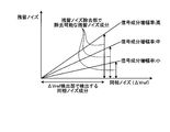
- FIG. 12 is a graph for explaining the transmission noise elimination effect according to the second embodiment.
- the vertical axis represents the residual noise level
- the horizontal axis represents the level of the in-phase noise ( ⁇ Vref) detected by the residual noise calculation unit 161.
- the residual noise calculation unit 161 multiplies the detected common-mode noise ( ⁇ Vref) by the amplification factor of the signal component, Residual noise components can be removed according to the amplification factor. If the amplification factor of the signal component is high, the level of the residual noise component removed by the residual noise removal unit 162 also becomes high. If the amplification factor of the signal component is low, the level of the residual noise component removed by the residual noise removal unit 162 Also lower.
- the level variation of the common-mode noise component is detected by extracting the DC component of the reference voltage, and the common-mode noise component is extracted from the signal component based on the detected level variation. It can be removed. Further, by amplifying the detected common-mode noise component at the same amplification factor as the signal component, it is possible to effectively remove the common-mode noise component whose level has been increased by amplification.
- FIG. 13 is a block diagram illustrating functions of the endoscope system according to the third embodiment.
- the same components as those in the endoscope system according to the first or second embodiment are denoted by the same reference numerals, and detailed description thereof is omitted. To do.
- An endoscope system 301 includes an imaging unit (endoscope) 102 that alternately outputs an imaging signal and a reference signal (constant voltage signal), and a predetermined signal as an imaging signal output by the imaging unit 102.
- the connector unit 305 that removes residual noise from the imaging signal based on the reference signal output from the imaging unit 102, the image signal output from the connector unit 305 is subjected to predetermined image processing, and the endoscope system
- a processor (control device) 6 that controls the entire unit 301 and a display device 7 that displays an image signal processed by the processor 6 are provided.
- the imaging unit 102 is an imaging device that can alternately output an imaging signal and a reference signal. As long as the imaging signal and the reference signal can be output, the image sensor of the imaging unit 102 may be any type of image sensor. In the third embodiment, a case where the imaging unit 102 is a CCD image sensor will be described.
- the reference signal transmitted by the imaging unit 102 may be a reference voltage generated based on the power supply voltage unique to the imaging unit 102, or the power supply voltage is supplied from the processor 6 or the connector unit 305 to the imaging unit 102.
- a reference voltage (power supply voltage reference signal) generated by the imaging unit 102 based on the supplied power supply voltage may be used.
- the connector unit 305 receives an imaging signal and a reference signal (clamp signal) output from the imaging unit 102, and performs an analog front end (AFE) unit that performs signal amplification and analog-digital conversion.
- AFE analog front end
- 150 and an imaging signal processing unit 360 that performs residual noise removal processing on the digitally converted signal.
- the AFE unit 150 is substantially the same as that of the second embodiment, and includes a reception unit 151, a signal intensity measurement unit 152, an amplification factor setting unit 153, a signal component extraction unit 154, and signal amplification / analog-digital conversion (ADC).
- the imaging signal processing unit 360 includes, for example, an FPGA (Field Programmable Gate Array), and includes a residual noise calculation unit 161 and a residual noise removal unit 162 having the same functions as those in the second embodiment. Other configurations are the same as those in the second embodiment, and the imaging signal received by the receiving unit 151 is output with the residual noise component removed, output to the processor 6 as an image signal, and displayed on the display device 7 as an image. .
- FPGA Field Programmable Gate Array
- FIG. 14 is a conceptual diagram for explaining common-mode noise components during transmission in the third embodiment.
- a waveform TS represents a temporal variation in the signal level of the imaging signal and the reference signal transmitted from the imaging unit 102 having the CCD image sensor
- a waveform RS represents the imaging signal and the reference signal received by the receiving unit 151 in FIG. It represents the time variation of the signal level.
- clamping is performed at an intermediate value of the ternary waveform, so that the clamp level becomes the reference signal. Therefore, in the third embodiment, the clamp level is used as the reference signal.
- the signal level of the image pickup signal is constantly changing. However, for convenience of explanation, in FIG. 14, it is assumed that the signal level of the image pickup signal is also maintained at a constant level, and attention is paid only to the change of the reference signal (Vref). Yes.
- the signal level of the reference signal is maintained at a predetermined level during transmission, but is transmitted over a long distance via the transmission cable 3 so that in-phase noise during transmission is superimposed, As shown on the right side of FIG. 14, the in-phase level fluctuation occurs between the imaging signal and the reference signal.
- the DC component of the reference signal is extracted to extract the level fluctuation of the in-phase noise component, and the residual from the signal component based on the extracted level fluctuation.
- Remove common-mode noise components for example, for each reference signal, a difference from a predetermined level is calculated, and an average value of differences calculated for one pixel row is used as an in-phase noise component ( ⁇ Vref) to remove the in-phase noise component. Used to do.
- the in-phase noise component is not limited to the average value for one line, and may be a maximum value or an intermediate value.
- the method and configuration for removing the common-mode noise component remaining in the imaging signal are the same as in the second embodiment.
- the DC component of the reference signal is extracted to detect the level fluctuation of the in-phase noise component, and based on the detected level fluctuation, the signal component Therefore, it is possible to remove the in-phase noise component. Further, by amplifying the detected common-mode noise component at the same amplification factor as the signal component, it is possible to effectively remove the common-mode noise component whose level has been increased by amplification.
- the imaging device An imaging unit for imaging a subject; An imaging control unit that controls the imaging unit to output a reference signal of the imaging unit, and a sum signal obtained by adding the imaging signal and the reference signal; An imaging device communication unit that transmits the reference signal and the sum signal to the image signal processing device;
- the image signal processing apparatus includes: An image processing device communication unit that receives the reference signal and the sum signal from the imaging device; A measurement unit that measures the signal strength of the reference signal and the sum signal received by the image processing device communication unit; An amplification factor setting unit that sets a signal amplification factor based on the signal intensity measured by the measurement unit; An imaging signal calculation unit that calculates the reference signal and the sum signal based on the set signal amplification factor and outputs an imaging signal;
- An endoscope system comprising: an image signal processing unit that generates an image signal based on an imaging signal output by the imaging signal calculation
- the image signal processing device further includes: A power supply unit for supplying a power supply voltage to the imaging device;
- the imaging device further includes: A power supply voltage reference signal generating unit that generates a power supply voltage reference signal based on a power supply voltage supplied from the power supply unit;
Landscapes
- Engineering & Computer Science (AREA)
- Signal Processing (AREA)
- Multimedia (AREA)
- Health & Medical Sciences (AREA)
- Life Sciences & Earth Sciences (AREA)
- Surgery (AREA)
- Radiology & Medical Imaging (AREA)
- Molecular Biology (AREA)
- Optics & Photonics (AREA)
- Pathology (AREA)
- Biophysics (AREA)
- Physics & Mathematics (AREA)
- Biomedical Technology (AREA)
- Heart & Thoracic Surgery (AREA)
- Medical Informatics (AREA)
- Nuclear Medicine, Radiotherapy & Molecular Imaging (AREA)
- Animal Behavior & Ethology (AREA)
- General Health & Medical Sciences (AREA)
- Public Health (AREA)
- Veterinary Medicine (AREA)
- Transforming Light Signals Into Electric Signals (AREA)
- Endoscopes (AREA)
- Studio Devices (AREA)
Abstract
撮像装置は、光電変換素子と、第1の転送部と、電荷変換部と、電荷変換部リセット部と、信号出力部と、第1の転送線と、転送容量と、第2の転送部と、転送容量リセット部と、第2の転送線と、駆動部とを備え、前記第1の転送部をオフ状態にして、前記電荷変換部をリセットした後、前記電荷変換部の信号を前記第1の転送線へ出力するときに、前記転送容量をリセットするノイズ信号読み出し動作と、前記転送容量リセット部をオフ状態にして、前記第1の転送部をオン状態にして前記光電変換素子が蓄積する電荷を転送した後、前記電荷変換部の信号を前記第1の転送線へ出力する光ノイズ和信号読み出し動作と、により前記第1の転送線から前記第2の転送部を介して信号を出力させる。
Description
本発明は、撮像装置、撮像装置を備えた内視鏡システム及び撮像装置を備えたノイズ除去方法に関する。
従来、CMOS(Complementary Metal-Oxide Semiconductor)イメージセンサを有する撮像装置では、画素列ごとのトランジスタのばらつきによる固定パターンノイズと、単位画素内の電荷電圧変換部のリセットノイズとを除去するために、画素列毎にノイズ除去部を設けることが知られている(例えば、特許文献1参照)。
図15は、従来の撮像装置の構成を示す回路図である。この例では、撮像装置500がCMOSイメージセンサを有する場合を説明する。
撮像装置500は、例えば、内視鏡の先端部に配置され、受光部と読み出し部とを含む。受光部は、複数行複数列にわたって二次元マトリクス状に配置される複数の単位画素530と、各単位画素530から出力される信号を転送する垂直転送線539とから構成される。読み出し部は、垂直走査部(行選択回路)541と、画素列毎に設けられるノイズ除去部543と、水平走査部(列選択回路)558とから構成される。
各単位画素530は、入射光量に応じた信号電荷を蓄積するフォトダイオードと、フォトダイオードから転送される信号電荷を電圧変換する電荷変換部と、フォトダイオードから信号電荷を電荷変換部に転送する転送トランジスタと、電荷変換部に転送された信号電荷をリセットするリセットトランジスタと、行選択トランジスタと、行選択トランジスタがオン状態のときに、電圧変換された信号電荷の電圧レベルの変化をソースフォロアで対応する垂直転送線539に、撮像信号として出力する出力トランジスタと、を備える。
読み出し部は、垂直走査部(行選択回路)541により任意の行の行選択トランジスタをオン状態にして、撮像信号を垂直転送線539に読み出す。読み出された撮像信号は、ノイズ除去部543に入力され、ノイズ成分が除去される。その後、水平走査部558により画像情報として外部に出力される。
図16は、図15に示す撮像装置のノイズ除去部の構成を表す回路図である。ノイズ除去部543は、一端側が垂直転送線539に接続されたサンプルホールド用のトランジスタ544と、トランジスタ544の他端側に一端側が接続された結合コンデンサ(AC結合容量)CCと、AC結合容量CCの他端側とグラウンドとの間に接続された電荷蓄積用コンデンサ(サンプル容量)CSと、AC結合容量CCとサンプル容量CSとの接続ノードSNに接続される電位クランプ用トランジスタ545と、を備える。なお、接続ノードSNは、水平走査部558に接続される。
ノイズ除去部543は、まず、画素リセット時にサンプルホールド用のトランジスタ544をオン状態にして、AC結合容量CCにより、垂直転送線539によって転送されたノイズ信号を伝達し、電位クランプ用トランジスタ545を所定期間オン状態にして、サンプル容量CSにノイズ信号レベルをサンプルする。その後、撮像信号読み出し時に、再度、ノイズ信号を含む撮像信号(光ノイズ和信号)をAC結合容量CCにより伝達する。画素リセット後における撮像信号の電圧変化分が伝達されるので、結果として、光ノイズ和信号からノイズ信号を差し引いた撮像信号を取り出すことができる。
図16に示すノイズ除去部543は、画素列毎にAC結合容量CCとサンプル容量CSの2つのコンデンサが必要となる。画素数が増加すると、コンデンサの大きさが制約となり、撮像装置の小型化が困難になる。さらに、信号レベルをサンプルする際に、AC結合容量CCとサンプル容量CSの容量分割により、ゲインが低下し、S/N比が悪化する。これを抑制するためには、AC結合容量CCを大きくする必要があり、そうすると小型化がさらに困難になる。
また、内視鏡は、先端部に撮像装置を設け、先端部の撮像装置とプロセッサ等の制御装置とを数mの伝送ケーブルを介して接続している。そのため、撮像装置を内視鏡に用いる場合、撮像信号を伝送ケーブルを介して長距離伝送しなければならず、伝送途中でノイズが混入する可能性が非常に高い。しかしながら、撮像素子から撮像信号のみを伝送すると、伝送途中で混入するノイズを除去することが困難である。
本発明は、上記に鑑みてなされたものであって、小型化を図りつつも画質が低下しない撮像装置、内視鏡システム及びノイズ除去方法を提供することを目的とする。
上述した課題を解決し、目的を達成するために、本発明による撮像装置は、受光量に応じて光電変換を行い、電荷を蓄積する光電変換素子と、前記蓄積される電荷を転送する第1の転送部と、前記転送される電荷を電圧または電流信号へ変換する電荷変換部と、前記電荷変換部を第1の電圧にリセットする電荷変換部リセット部と、前記変換された信号を出力する信号出力部と、前記信号出力部と接続される第1の転送線と、前記第1の転送線と接続される転送容量と、前記転送容量を介して前記第1の転送線と接続され、前記転送容量の容量による結合により、前記第1の転送線から信号が出力される第2の転送部と、前記転送容量を第2の電圧にリセットする転送容量リセット部と、前記第2の転送部からの信号が出力される第2の転送線と、前記第1の転送部をオフ状態にして、前記電荷変換部リセット部により前記電荷変換部をリセットした後、前記信号出力部を介して前記電荷変換部の信号を前記第1の転送線へ出力するときに、前記転送容量リセット部により前記転送容量をリセットするノイズ信号読み出し動作と、前記転送容量リセット部をオフ状態にして、前記第1の転送部をオン状態にして前記光電変換素子が蓄積する電荷を転送した後、前記信号出力部を介して、前記電荷変換部の信号を前記第1の転送線へ出力する光ノイズ和信号読み出し動作と、により前記第1の転送線から前記第2の転送部を介して信号を出力させる駆動部と、を備えることを特徴とする。
本発明に係る撮像装置は、上記発明において、さらに、前記第2の電圧と同相の揺らぎ成分を持つ基準電圧を生成する基準電圧生成部と、前記第2の転送線と、前記基準電圧生成部とに接続され、前記第2の転送線から入力される信号と、前記基準電圧生成部から入力される前記基準電圧とを、選択して出力する出力選択部と、を備えることを特徴とする。
本発明に係る撮像装置は、上記発明において、さらに、前記第2の転送線を第3の電圧にリセットする第2の転送線リセット部と、前記第2の転送線と前記出力選択部との間に設けられるサンプルホールド部とを備え、前記光ノイズ和信号読み出し動作は、前記第1の転送線の信号を前記第2の転送線へ出力した時に、前記サンプルホールド部により前記第1の転送線から出力される信号をサンプルした後に、前記第2の転送線をリセットすることを繰り返すことにより、前記第1の転送線から出力される信号のみを前記出力選択部に入力することを特徴とする。
本発明に係る撮像装置は、上記発明において、さらに、前記第1の電圧に基づく基準電圧を生成する基準電圧生成部を備え、前記基準電圧生成部は、当該基準電圧生成部の電圧を前記第1の電圧にリセットする基準電圧生成部リセット部と、前記基準電圧生成部リセット部の信号を出力する基準電圧生成部信号出力部と、前記基準電圧生成部信号出力部からの信号を、前記基準電圧として前記第2の転送線へ出力する第3の転送部と、を備え、前記駆動部は、前記第1の転送線から出力される信号と前記基準電圧とが交互に前記第2の転送線へ出力されるように、前記第2の転送部及び前記第3の転送部を駆動することを特徴とする。
本発明に係る内視鏡システムは、上記発明における撮像装置と、前記撮像装置の出力する前記第1の転送線から出力される信号と前記基準電圧とを送信する送信部と、前記送信部が送信する信号を受信する受信部と、前記受信部が受信する信号を演算する演算部と、を備えることを特徴とする。
本発明に係る内視鏡システムは、上記発明において、前記演算部が、前記受信部が受信する信号の信号強度を測定する信号強度測定部と、前記測定した信号強度に基づき、前記受信部が受信する信号の増幅率を設定する増幅率設定部と、前記増幅率と、前記基準電圧とに基づき、前記第1の転送線から出力される信号と前記基準電圧とを演算し、前記第1の転送線から出力される信号から伝送時の同相ノイズ成分を差し引いた撮像信号を出力する撮像信号演算部と、を備えることを特徴とする。
本発明に係る内視鏡システムは、上記発明において、前記撮像信号演算部が、前記基準電圧の直流成分を抽出する直流成分抽出部と、前記増幅率と、前記直流成分とに基づき、前記第1の転送線から出力される信号に含まれる伝送時の同相ノイズ成分を除去するノイズ成分除去部とを備えることを特徴とする。
本発明に係るノイズ除去方法は、受光量に応じて光電変換を行い、電荷を蓄積する光電変換素子と、前記蓄積される電荷を転送する第1の転送部と、前記転送される電荷を電圧または電流信号へ変換する電荷変換部と、前記電荷変換部を第1の電圧にリセットする電荷変換部リセット部と、前記変換された信号を出力する信号出力部と、前記信号出力部と接続される第1の転送線と、前記第1の転送線と接続される転送容量と、前記転送容量を介して前記第1の転送線と接続され、前記転送容量の容量による結合により、前記第1の転送線から信号が出力される第2の転送部と、前記転送容量を第2の電圧にリセットする転送容量リセット部と、前記第2の転送部からの信号が出力される第2の転送線と、を備える撮像装置におけるノイズ除去方法であって、前記第1の転送部をオフ状態にして、前記電荷変換部リセット部により前記電荷変換部をリセットする工程と、前記信号出力部を介して前記電荷変換部の信号を前記第1の転送線へ出力するときに、前記転送容量リセット部により前記転送容量をリセットする工程と、前記転送容量リセット部をオフ状態にして、前記第1の転送部をオン状態にして前記光電変換素子が蓄積する電荷を転送する工程と、前記信号出力部を介して、前記電荷変換部の信号を前記第1の転送線へ出力する工程と、前記第1の転送線から前記第2の転送部を介して信号を出力させる工程とを備えることを特徴とする。
本発明によれば、小型化を図りつつも画質が低下しない撮像装置、内視鏡システム及びノイズ除去方法を提供することができる。
以下の説明では、本発明を実施するための形態(以下、「実施の形態」という)として、撮像装置を備えた内視鏡システムについて説明する。また、この実施の形態により、この発明が限定されるものではない。さらに、図面の記載において、同一部分には同一の符号を付している。さらにまた、図面は、模式的なものであり、各部材の厚みと幅との関係、各部材の比率等は、現実と異なることに留意する必要がある。また、図面の相互間においても、互いの寸法や比率が異なる部分が含まれている。
(実施の形態1)
図1は、本発明の実施の形態1による内視鏡システムの全体構成を模式的に示す図である。同図に示す内視鏡システム1は、内視鏡2と、伝送ケーブル3と、コネクタ部5と、プロセッサ(制御装置)6と、表示装置7と、光源装置8と、を備える。内視鏡2は、被検体の体腔内に先端部を挿入することによって被検体の体内画像を撮像して撮像信号を出力する。伝送ケーブル3は、内視鏡2とコネクタ部5を接続する。コネクタ部5は、内視鏡2、プロセッサ6及び光源装置8に接続され、接続された内視鏡2が出力する撮像信号に所定の信号処理を施すとともに、撮像信号をアナログデジタル変換(A/D変換)して画像信号として出力する。プロセッサ6は、コネクタ部5から出力される画像信号に所定の画像処理を施すとともに、内視鏡システム1全体を制御する。表示装置7は、プロセッサ6が処理を施した画像信号を表示する。光源装置8は、例えば、白色LEDを用いて構成される。光源装置8が点灯するパルス状の白色光は、コネクタ部5、伝送ケーブル3を経由して内視鏡2の挿入部の先端部へ達し、その先端部から被写体へ向けて照射する照明光となる。
図1は、本発明の実施の形態1による内視鏡システムの全体構成を模式的に示す図である。同図に示す内視鏡システム1は、内視鏡2と、伝送ケーブル3と、コネクタ部5と、プロセッサ(制御装置)6と、表示装置7と、光源装置8と、を備える。内視鏡2は、被検体の体腔内に先端部を挿入することによって被検体の体内画像を撮像して撮像信号を出力する。伝送ケーブル3は、内視鏡2とコネクタ部5を接続する。コネクタ部5は、内視鏡2、プロセッサ6及び光源装置8に接続され、接続された内視鏡2が出力する撮像信号に所定の信号処理を施すとともに、撮像信号をアナログデジタル変換(A/D変換)して画像信号として出力する。プロセッサ6は、コネクタ部5から出力される画像信号に所定の画像処理を施すとともに、内視鏡システム1全体を制御する。表示装置7は、プロセッサ6が処理を施した画像信号を表示する。光源装置8は、例えば、白色LEDを用いて構成される。光源装置8が点灯するパルス状の白色光は、コネクタ部5、伝送ケーブル3を経由して内視鏡2の挿入部の先端部へ達し、その先端部から被写体へ向けて照射する照明光となる。
内視鏡2は、被検体の体腔内に挿入される挿入部の先端側に、体内画像の撮像を行う撮像部(撮像装置)20が設けられ、挿入部の基端側に、内視鏡2に対する各種操作を受け付ける操作部4が接続される。撮像部20は、伝送ケーブル3により、操作部4を介して、コネクタ部5に接続される。撮像部20が撮像した画像の撮像信号は、例えば、数mの長さを有する伝送ケーブル3を通り、コネクタ部5に出力される。
図2は、本発明の実施の形態1による内視鏡システムの要部の機能を表すブロック図である。図2を参照して、内視鏡システム1の各構成の詳細及び内視鏡システム1内の電気信号の経路を説明する。
撮像部20は、受光部23を有する第1チップ21と、バッファ27を有する第2チップ22とを含む。第1チップ21と第2チップ22は相対して貼り合わされ、チップ間は、チップの周縁部に配置されるパッド、またはチップ間を貫通するビア等により接続される。なお、第1チップ21と第2チップ22は、双方の主面が平行になるように配置するものに限らず、周囲の構造により、横に並べて配置したり、一方の主面に対して他方の主面が垂直になるように配置したりしてもよい。
撮像部20の第1チップ21は、多数の単位画素が行列方向に二次元マトリクス状に配置される受光部23と、受光部23で光電変換された撮像信号を読み出す読み出し部24と、コネクタ部5から送出される基準クロック信号及び同期信号に基づきタイミング信号を生成して読み出し部24に供給するタイミング生成部25と、撮像信号を第2チップ22に出力するマルチプレクサ26と、を含む。なお、第1チップ21のより詳細な構成については、図3を参照して後に詳述する。
撮像部20の第2チップ22は、伝送ケーブル3及びコネクタ部5を介して、第1チップ21から出力される撮像信号の交流成分のみをプロセッサ6へ送信する送信部として機能するバッファ27を含む。なお、第1チップ21と第2チップ22に搭載される回路の組み合わせは設計の都合に合わせて適宜変更可能である。
また、撮像部20は、伝送ケーブル3を介して、プロセッサ6内の電源部61で生成された電源電圧(VDD)をグラウンド(GND)とともに受け取る。撮像部20に供給された電源電圧(VDD)とグラウンド(GND)の間には、電源安定用のコンデンサC1が設けられる。
コネクタ部5は、アナログ・フロント・エンド(AFE)部51と撮像信号処理部52とを含む。コネクタ部5は、内視鏡2(撮像部20)とプロセッサ6とを電気的に接続し、電気信号を中継する中継処理部として機能する。コネクタ部5と撮像部20とは伝送ケーブル3で接続され、コネクタ部5とプロセッサ6とは、例えば、コイルケーブルにより接続される。また、コネクタ部5は、光源装置8にも接続されている。
AFE部51は、撮像部20から伝送される撮像信号を受信し、抵抗などの受動素子でインピーダンスマッチングを行った後、コンデンサで交流成分を取り出し、分圧抵抗で動作点を決定する。その後、AFE部51は、アナログ撮像信号を、アナログデジタル(A/D)変換して、デジタル撮像信号として、撮像信号処理部52に送出する。
撮像信号処理部52は、例えば、FPGA(Field Programmable Gate Array)により構成され、内視鏡2の各構成部の動作の基準となる基準クロック信号(例えば、27MHzのクロック)及び各フレームのスタート位置を表す同期信号を生成して、タイミング生成部25に供給するとともに、AFE部51から入力されるデジタル撮像信号に対してノイズ除去等の所定の信号処理を行う。
プロセッサ6は、電源部61と画像信号処理部62とを含んで構成され、内視鏡システム1の全体を制御する制御装置である。電源部61は、電源電圧(VDD)を生成し、この生成した電源電圧をグラウンド(GND)とともに、コネクタ部5及び伝送ケーブル3を介して、撮像部20に供給する。画像信号処理部62は、撮像信号処理部52でノイズ除去等の信号処理が施されたデジタル撮像信号に対して、所定の画像処理を行い、画像信号として、表示装置7に出力する。
表示装置7は画像信号に基づき、撮像部20が撮像した画像を表示する。画像信号処理部62における画像処理は、例えば、同時化処理、ホワイトバランス(WB)調整処理、ゲイン調整処理、ガンマ補正処理、デジタルアナログ(D/A)変換処理、フォーマット変換処理等である。
図3は、図2に示す第1チップの詳細な構成を示すブロック図である。図4は、実施の形態1による内視鏡システムの第1チップの構成を示す回路図である。第1チップ21には、例えば、受光部23と、読み出し部(駆動部)24と、タイミング生成部25と、マルチプレクサ26とが搭載される。受光部23の詳細については、図4を参照して後述する。なお、タイミング生成部25の前段、すなわち、タイミング生成部25の入力とプロセッサ6間には、ヒステリシス回路28が設けられている。ヒステリシス回路28は、伝送ケーブル3により長距離伝送された基準クロック信号及び同期信号の波形整形を行う。ヒステリシス回路28で波形整形された基準クロック信号及び同期信号は、タイミング生成部25に入力される。
タイミング生成部25は、ヒステリシス回路28で整形された基準クロック信号及び同期信号に基づき、各種駆動信号(φTa、φTb、φR、φX、φVCL、φHCLR、φHCLK、φMUXSEL、φVSH)を生成し、垂直走査部241、ノイズ除去部243、水平走査部245、マルチプレクサ26、及び基準電圧生成部246に供給する。
読み出し部24は、垂直走査部(行選択回路)241と、定電流源242と、ノイズ除去部243と、列ソースフォロアバッファ(トランジスタ)244と、水平走査部(列選択回路)245と、基準電圧生成部246と、を含む。
垂直走査部241は、タイミング生成部25から供給される駆動信号(φT、φR、φX)に基づき、受光部23の選択された行<N>(N=0,1,2,…,n-1,n)に行選択パルスφTa<N>、φTb<N>、φR<N>及びφX<N>を印加して、受光部23の各単位画素230を定電流源242で駆動し、撮像信号及び画素リセット時のノイズ信号を垂直転送線239に転送し、ノイズ除去部243に出力する。
ノイズ除去部243は、各単位画素230ごとの出力ばらつきと、画素リセット時のノイズ信号とを除去し、各単位画素230で光電変換された撮像信号を列ソースフォロアバッファ244に出力する。なお、ノイズ除去部243の詳細は、図4を参照して後述する。
水平走査部245は、タイミング生成部25から供給される駆動信号(φHCLK)に基づき、受光部23の選択された列<M>(M=0,1,2,…,m-1,m)に列選択パルスφHCLK<M>を印加し、各単位画素230で光電変換された撮像信号を列ソースフォロアバッファ244を介して、水平転送線258に転送し、マルチプレクサ26に出力する。
マルチプレクサ26は、タイミング生成部25から供給される駆動信号(φMUXSEL)により駆動され、水平転送線258を通じて入力される撮像信号と基準電圧生成部246で生成される基準電圧Vref(定電圧信号)とを交互に、出力部(アンプ)31を介して、第2チップ22に出力する。ここで出力される基準電圧Vrefは、コネクタ部5の撮像信号処理部52等において、撮像信号伝送時の伝送ケーブル3で重畳される同相ノイズ除去のために利用される。なお、必要に応じて、マルチプレクサ26の入力側にゲイン調整のためのアンプを設けてもよい。
第1チップ21の受光部23には、多数の単位画素230が二次元マトリクス状に配列される。各単位画素230は、光電変換素子(フォトダイオード)231及び232と、電荷変換部233と、転送トランジスタ(第1の転送部)234及び235と、電荷変換部リセット部(トランジスタ)236と、画素ソースフォロアトランジスタ237及び画素出力スイッチ(信号出力部)238と、を含む。なお、本明細書では、1又は複数の光電変換素子と、それぞれの光電変換素子から信号電荷を電荷変換部233に転送するための転送トランジスタとを単位セルと呼ぶ。すなわち、単位セルには1又は複数の光電変換素子と転送トランジスタの組が含まれ、各単位画素230には、1つの単位セルが含まれる。
光電変換素子231及び232は、入射光をその光量に応じた信号電荷量に光電変換して蓄積する。光電変換素子231及び232のカソード側は、それぞれ転送トランジスタ234及び235の一端側に接続され、アノード側はグラウンドGNDに接続される。電荷変換部233は、浮遊拡散容量(FD)からなり、光電変換素子231及び232で蓄積された電荷を電圧に変換する。
転送トランジスタ234及び235は、それぞれ光電変換素子231及び232から電荷変換部233に電荷を転送する。転送トランジスタ234及び235のそれぞれのゲートには、駆動パルス(行選択パルス)φTa及びφTbが供給される信号線が接続され、他端側は電荷変換部233に接続される。垂直走査部241から信号線を介して駆動パルスφTa及びφTbが供給されると、転送トランジスタ234及び235がオン状態となり、光電変換素子231及び232から電荷変換部233に信号電荷が転送される。
電荷変換部リセット部(トランジスタ)236は、電荷変換部233を所定電位にリセットする。電荷変換部リセット部236は、一端側が電源電圧VDDに接続され、他端側が電荷変換部233に接続され、ゲートには駆動パルスφRが供給される信号線が接続される。垂直走査部241から信号線を介してφRが供給されると、電荷変換部リセット部236がオン状態となり、電荷変換部233に蓄積された信号電荷が放出されて、電荷変換部233が所定電位にリセットされる。
画素ソースフォロアトランジスタ237は、一端側が電源電圧VDDに接続され、他端側が画素出力スイッチ238の一端側に接続される。ゲートには電荷変換部233で電圧変換された信号(撮像信号又はリセット時の信号)が入力される。画素出力スイッチ238は、電荷変換部233で電圧変換された信号を垂直転送線239に出力する。画素出力スイッチ238の他端側は垂直転送線239に接続され、ゲートには、駆動パルスφXが供給される信号線が接続される。画素出力スイッチ238のゲートに垂直走査部241から信号線を介して駆動パルスφXが供給されると、画素出力スイッチ238がオン状態となり、撮像信号又はリセット時の信号が垂直転送線239に転送される。
定電流源242は、一端側が垂直転送線239に接続され、他端側がグラウンドGNDに接続され、ゲートにはバイアス電圧Vbias1が印加される。単位画素230を定電流源242で駆動し、単位画素230の出力を垂直転送線239へ読み出す。垂直転送線239へ読み出された信号は、ノイズ除去部243に入力される。
ノイズ除去部243は、転送容量(AC結合コンデンサ)252と、クランプスイッチ(トランジスタ)253と、を含む。転送容量252は、一端側が垂直転送線239に接続され、他端側が列ソースフォロアトランジスタ244に接続される。クランプスイッチ253は、一端側が基準電圧生成部246からクランプ電圧Vclpが供給される信号線に接続される。クランプスイッチ253の他端側は、転送容量252と列ソースフォロアトランジスタ244間に接続され、ゲートには、タイミング生成部25から駆動信号φVCLが入力される。ノイズ除去部243に入力される撮像信号はノイズ成分を含んだ光ノイズ和信号である。
タイミング生成部25から、駆動信号φVCLがクランプスイッチ253のゲートに入力されると、クランプスイッチ253がオン状態となり、転送容量252は、基準電圧生成部246から供給されるクランプ電圧Vclpによりリセットされる。ノイズ除去部243でノイズ除去された撮像信号は、列ソースフォロアトランジスタ244のゲートに入力される。
ノイズ除去部243は、サンプリング用のコンデンサ(サンプリング容量)を必要としないため、転送容量(AC結合コンデンサ)252の容量は、列ソースフォロアトランジスタ244の入力容量に対する十分な容量であればよい。加えて、ノイズ除去部243は、サンプリング容量の無い分、第1チップ21における占有面積を小さくすることができる。
列ソースフォロアトランジスタ244の一端側は、電源電圧VDDに接続され、他端側は列選択スイッチ(第2の転送部)254の一端側に接続され、ゲートにはノイズ除去部243でノイズ除去された撮像信号が入力される。列選択スイッチ254の一端側は、列ソースフォロアトランジスタ244の他端側に接続され、他端側は水平転送線(第2の転送線)258に接続される。列選択スイッチ254のゲートには、水平走査部245から駆動信号φHCLK<M>を供給するための信号線が接続される。列<M>の列選択スイッチ254のゲートに水平走査部245から駆動信号φHCLK<M>が供給されると、列選択スイッチ254がオン状態となり、列<M>の垂直転送線239の信号(ノイズ除去部243でノイズ除去された撮像信号)が水平転送線258に転送される。
定電流源257は、一端側が水平転送線258に接続され、他端側がグラウンドGNDに接続され、ゲートにはバイアス電圧Vbias2が印加される。定電流源257は撮像信号を垂直転送線239から水平転送線258へ読み出す。水平転送線258へ読み出された信号は、サンプルホールド部255に入力される。
水平リセットトランジスタ256の一端側は水平リセット電圧Vclrに接続され、他端側は水平転送線258に接続される。水平リセットトランジスタ256のゲートには、タイミング生成部25から駆動信号φHCLRが入力される。タイミング生成部25から駆動信号φHCLRが水平リセットトランジスタ256のゲートに入力されると、水平リセットトランジスタ256がオン状態となり、水平転送線258がリセットされる。
サンプルホールド部255は、バッファ261と、サンプルホールドスイッチ(トランジスタ)262と、サンプル容量(コンデンサ)263と、オペアンプ264と、を含む。バッファ261の入力には、水平転送線258が接続され、該水平転送線258を介して、撮像信号と水平リセット時のノイズ信号とがバッファ261に入力される。バッファ261の出力は、サンプルホールドスイッチ262の一端側に接続される。サンプルホールドスイッチ262の他端側は、オペアンプ264の入力に接続される。サンプル容量263の一端側は、サンプルホールドスイッチ262の他端側とオペアンプ264の入力とに接続され、他端側はグラウンドGNDに接続される。オペアンプ264の出力は、オペアンプ264に反転入力端子に接続されるとともに、マルチプレクサ26の入力に接続される。サンプルホールド部255は、サンプルホールドスイッチ262がオフ状態になる直前の電圧をサンプル容量263に保持し、サンプルホールドスイッチ262がオフ状態になっている間は、サンプル容量263に保持した電圧を出力する。
実施の形態1では、垂直転送線239からのノイズ除去後の撮像信号の読み出しと、水平リセットトランジスタ256による水平転送線258のリセットとを交互に行うことにより、列方向の撮像信号のクロストークを抑制することが可能となる。また、サンプルホールド部255のサンプルホールドスイッチ262を、ノイズ除去後の撮像信号の転送時にオン状態とし、リセット時のノイズ信号の転送時にオフ状態とすることにより、ノイズ除去後の撮像信号のみをオペアンプ264に出力することが可能となる。第1チップ21がサンプルホールド部255を備えることにより、後段の増幅回路の帯域を半分にするとともに、レンジを抑制することができる。
マルチプレクサ26は、サンプルホールド部255から出力されるノイズ除去された撮像信号と、基準電圧生成部246で生成される基準電圧Vrefとを交互に、出力部31に出力する。出力部31は、ノイズ除去された撮像信号と基準電圧Vrefとを必要に応じて信号増幅して、交互に第2チップ22に出力する。
第2チップ22では、ノイズ除去された撮像信号と基準電圧Vrefとの交流成分のみを、伝送ケーブル3を介して、コネクタ部5に伝送する。
図5は、実施の形態1による内視鏡システムの受光部の基準電圧生成部の構成を示す回路図である。基準電圧生成部(定電圧信号生成部)246は、2つの抵抗291及び292からなる抵抗分圧回路と、駆動信号φVSHで駆動されるスイッチ(トランジスタ)293と、電源から独立させて、揺らぎから開放させるためのサンプリング容量(コンデンサ)294と、を含む。基準電圧生成部246は、スイッチ293の駆動により駆動信号φVSHが駆動するタイミングで、受光部23と同じ電源電圧VDDから基準電圧Vref(定電圧信号)と、ノイズ除去部243のクランプ電圧Vclpとを生成する。
基準電圧Vrefとクランプ電圧Vclpとが同じ電源から同じタイミングで生成されるため、基準電圧Vrefは、ノイズ除去部243から出力される撮像信号に対する電源揺らぎの影響を反映する。また、基準電圧Vrefは、伝送ケーブル3での伝送ノイズ情報を伝送中に反映する。したがって、ノイズ除去された撮像信号と基準電圧Vrefとを交互にコネクタ部5に伝送することにより、コネクタ部5において、相関二重サンプリング等のノイズ除去処理を行い、伝送中のノイズを除去した撮像信号を得ることができる。
図6は、実施の形態1による撮像装置の駆動信号を示すタイミングチャートである。この例では、受光部23の行<n>の単位画素230から信号を読み出し、出力部31から出力されるまでを説明する。
まず、クランプスイッチ253をオン(φVCLがHigh)し、画素出力スイッチ238をオン(φX<n>がHigh)、電荷変換部リセット部236をパルス状にオン(駆動パルスφR<n>がHigh)、転送トランジスタ234及び235をオフ(駆動パルスφTa<n>及びφTb<n>がLow)することにより、読み出し対象の単位画素230特有のばらつきと、画素リセット時のノイズなどを含むノイズ信号を、単位画素230から垂直転送線239に出力する。このとき、クランプスイッチ253をオン(φVCLがHigh)状態にしたままにすることにより、列ソースフォロアトランジスタ244のゲートをクランプ電圧Vclpの電圧とする。クランプ電圧Vclpは、φVSHの立下りのタイミングで決定し、このタイミングで基準電圧Vrefも決定される。
次に、クランプスイッチ253をオフ(φVCLがLow)にした状態で、転送トランジスタ234をパルス状にオン(駆動パルスφTa<n>がHigh)することにより、光電変換素子231で光電変換された電荷を電荷変換部233が変換した信号を垂直転送線239に読み出す。この状態で、画素出力スイッチ238はオン(φX<n>がHigh)されたままであるので、電荷変換部233によって電圧変換された撮像信号(光ノイズ和信号)は垂直転送線239に転送される。この動作により、転送容量252を介して、ノイズ信号が差し引かれた撮像信号(光信号)が、列ソースフォロアトランジスタ244のゲートに出力される。ここで列ソースフォロアトランジスタ244のゲートに出力される信号は、クランプ電圧Vclpを基準としてサンプリングされた信号である。
撮像信号をクランプ電圧Vclpを基準としてサンプリングした後、水平リセットトランジスタ256をオフ(φHCLRがLow)にし、水平転送線258のリセットを解除し、列<0>の列選択スイッチ254をオン(駆動パルスφHCLK<0>がHigh)することにより、撮像信号を水平転送線258に転送する。この時、サンプルホールドスイッチ262をパルス状にオン(駆動パルスφHSHがHigh)することにより、撮像信号がサンプル容量263にサンプリングされる。その後、マルチプレクサ26にLowレベルの駆動パルスφMUXSELを印加して、サンプル容量263にサンプリングされた撮像信号を出力部31に出力する。この時、マルチプレクサ26の駆動パルスと同期して、水平リセットトランジスタ256をオン(駆動パルスφHCLRがHigh)にし、水平転送線258を再度リセットする。
さらにその後、マルチプレクサ26にHighレベルの駆動パルスφMUXSELを印加し、基準電圧生成部246で生成した基準電圧Vref(定電圧信号)を出力部31に出力するとともに、水平リセットトランジスタ256をオフ(φHCLRがLow)にし、リセットされていた水平転送線258のリセットを解除し、次の列の列選択スイッチ254をオン(φHCLK<1>がHigh)することにより、撮像信号を水平転送線258に転送する。この時、サンプルホールドスイッチ262をパルス状にオン(駆動パルスφHSHがHigh)することにより、撮像信号がサンプル容量263にサンプリングされる。そして、水平リセットトランジスタ256をオン(φHCLRがHigh)にし、水平転送線258を再度リセットするとともに、水平リセットトランジスタ256のパルスと同期して、マルチプレクサ26にLowレベルの駆動パルスφMUXSELを印加して、サンプリングされた撮像信号を出力部31に出力する。
このような動作を、受光部23の列数分(又は読み出しが必要な列数分)繰り返すことにより、撮像信号と基準電圧Vrefとが交互に出力部31から出力される。さらに、光電変換素子232についても、同一の動作を行うことにより、1ライン分の撮像信号が出力される。また、1ライン分の読み出し動作を単位画素行数分(又は読み出しが必要な行数分)繰り返すことにより、1フレーム分の撮像信号が出力される。
以上、本発明の実施の形態1によれば、ノイズ除去部243に、サンプリング用のコンデンサ(サンプリング容量)を必要としないため、転送容量(AC結合コンデンサ)252の容量を低く抑えることができる。また、サンプリング容量が無い分、ノイズ除去部243の占有面積を小さくすることができる。
さらに、本発明の実施の形態1によれば、1画素ごとに撮像信号と基準電圧Vrefとを交互に出力することができる。これにより、例えば、コネクタ部5に設けられる相関二重サンプリング回路で、信号の伝送中に重畳する同相ノイズを効果的に除去することができる。
なお、上述の実施の形態1では、列方向に隣り合う2つの光電変換素子231及び232を一組として単位セルを構成したが、行方向に隣り合う2つの光電変換素子を一組として単位セルを構成してもよいし、行方向及び列方向に隣り合う4つの光電変換素子を一組として単位セルを構成してもよい。また、画素共有を行わずに、1つの光電変換素子で単位セルを構成するようにしてもよい。
なお、サンプルホールド部255は、省略可能である。サンプルホールド部255を省略した場合でも、後段のマルチプレクサ26により、撮像信号のみが選択され、出力部31には、撮像信号と基準電圧Vrefとが交互に出力される。
(実施の形態1の変形例)
図7は、実施の形態1の変形例による内視鏡システムの第1チップの構成を示す回路図である。この実施の形態1の変形例による内視鏡システム1の説明においては、実施の形態1による内視鏡システム1と同一の構成要素については同一の符号を付して、その詳細な説明は省略する。
図7は、実施の形態1の変形例による内視鏡システムの第1チップの構成を示す回路図である。この実施の形態1の変形例による内視鏡システム1の説明においては、実施の形態1による内視鏡システム1と同一の構成要素については同一の符号を付して、その詳細な説明は省略する。
この実施の形態1の変形例では、図4の水平リセットトランジスタ256の代わりに、基準電圧生成部356を、垂直走査部241とタイミング生成部25との間に接続するとともに、列<0>のノイズ除去部243を介して、水平転送線258に接続している。また、この変形例では、画素共有を行わずに1つの光電変換素子231が単位画素230に含まれている。それ以外の回路構成は、実施の形態1と同様である。
基準電圧生成部356は、リセット部(トランジスタ)336と、ソースフォロアトランジスタ337及び出力スイッチ(トランジスタ)338と、を含む。リセット部336は、一端側が電源電圧VDDに接続され、他端側がソースフォロアトランジスタ337のゲートに接続され、ゲートには駆動パルスφRが供給される信号線が接続される。タイミング生成部25から信号線を介して駆動パルスφRが供給されると、リセット部336がオン状態となり、ソースフォロアトランジスタ337のゲートにリセット時の信号が入力される。ソースフォロアトランジスタ337は、一端側が電源電圧VDDに接続され、他端側が出力スイッチ338の一端側に接続される。出力スイッチ338の他端側は垂直転送線339に接続され、ゲートには、駆動パルスφXが供給される信号線が接続される。出力スイッチ338のゲートにタイミング生成部25から信号線を介して駆動パルスφXが供給されると、出力スイッチ338がオン状態となり、リセット時の信号が基準電圧生成部356用の垂直転送線339に転送される。垂直転送線339に転送されたリセット時の信号(基準電圧Vclp)は、ノイズ除去部243により、ノイズが除去されて、水平転送線258に転送される。
基準電圧生成部356に供給される駆動パルスφR及び駆動パルスφXは、垂直走査部241を介さずに、タイミング生成部25から直接供給されるので、行選択のためのインデックスが付されておらず、どの行が選択されているときでも、基準電圧生成部356には、駆動パルスφR及び駆動パルスφXが供給される。
以上のように、この実施の形態1の変形例では、水平リセット時の信号の代わりに、通常の撮像信号と同じような経路を通過した基準電圧を水平転送線258に転送することで、単位画素230から転送される途中で混入するノイズ成分を含んだ信号を水平転送線258に転送することができる。
図8は、実施の形態1の変形例による内視鏡システムの受光部の基準電圧生成部の構成を示す回路図である。基準電圧生成部246bは、2つの抵抗291及び292からなる抵抗分圧回路と、駆動信号φVSHで駆動されるスイッチ(トランジスタ)293と、容量(コンデンサ)294と、を含む。基準電圧生成部246bは、駆動信号φVSHのタイミングで、受光部23と同じ電源電圧VDDからノイズ除去部243のクランプ電圧Vclpを生成する。この変形例では、基準電圧生成部356において生成した電圧を基準電圧Vrefの代わりに、コネクタ部5に伝送するため、基準電圧生成部246bでは、基準電圧Vrefを出力せずに、クランプ電圧Vclpのみを出力している。その他の構成は、実施の形態1による基準電圧生成部246と同様である。
図9は、実施の形態1の変形例1による撮像装置の駆動信号を示すタイミングチャートである。まず、クランプスイッチ253をオン(φVCLがHigh)にし、画素出力スイッチ238をオン(φX<n>がHigh)、電荷変換部リセット部236をオン(駆動パルスφR<n>がHigh)、転送トランジスタ234及び235をオフ(駆動パルスφT<n>がLow)することにより、行<n>の単位画素230特有のばらつき及び画素リセット時のノイズなどを含むノイズ信号を、単位画素230から垂直転送線239に出力する。この時、基準電圧生成部356の出力スイッチ338もオン(φXがHigh)、リセット部336もオン(駆動パルスφRがHigh)されるので、基準電圧生成部356からも基準電圧が垂直転送線339に出力される。また、クランプスイッチ253をオン(φVCLがHigh)状態にしたままにすることにより、列ソースフォロアトランジスタ244のゲートをクランプ電圧Vclpの電圧とする。クランプ電圧Vclpは、φVSHの立下りのタイミングで決定し、このタイミングで基準電圧Vrefも決定される。
次に、クランプスイッチ253をオフ(φVCLがLow)にした状態で、転送トランジスタ234をオン(駆動パルスφT<n>がHigh)することにより、光電変換素子231で光電変換された電荷を電荷変換部233に読み出す。この時、画素出力スイッチ238はオン(φX<n>がHigh)されたままであるので、電圧変換された撮像信号は垂直転送線239に転送される。この動作により、転送容量252を介して、ノイズ信号が差し引かれた撮像信号が、列ソースフォロアトランジスタ244のゲートに出力される。ここで列ソースフォロアトランジスタ244のゲートに出力される信号は、クランプ電圧Vclpを基準としてサンプリングされた信号である。
撮像信号をクランプ電圧Vclpを基準としてサンプリングした後、基準電圧生成部356に対応する列<0>の列選択スイッチ354をオン(駆動パルスφHCLK<0>がHigh)することにより、基準電圧生成部356が出力する基準電圧(クランプ電圧Vclp)を水平転送線258に転送する。その後、列<0>の列選択スイッチ354をオフ(駆動パルスφHCLK<0>がLow)にし、列<1>の列選択スイッチ254をオン(駆動パルスφHCLK<1>がHigh)することにより、撮像信号を水平転送線258に転送する。さらにその後、列<1>の列選択スイッチ254をオフ(駆動パルスφHCLK<1>がLow)にして、再度、基準電圧生成部356に対応する列<0>の列選択スイッチ354をオン(駆動パルスφHCLK<0>がHigh)することにより、基準電圧生成部356が出力する基準電圧(ノイズ信号)を水平転送線258に転送する。次に、列<0>の列選択スイッチ354をオフ(駆動パルスφHCLK<0>がLow)にし、列<2>の列選択スイッチ254をオン(駆動パルスφHCLK<2>がHigh)することにより、次の列の撮像信号を水平転送線258に転送する。このような動作を、受光部23の列数分(又は読み出しが必要な列数分)繰り返すことにより、基準電圧生成部356が出力する基準電圧と撮像信号(撮像信号と基準電圧が加算された撮像信号基準電圧和信号)とが交互に出力部31から出力される。
以上、本発明の実施の形態1の変形例によれば、実施の形態1と同様に、ノイズ除去部243に、サンプリング用のコンデンサ(サンプリング容量)を必要としないため、転送容量(AC結合コンデンサ)252の容量を低く抑えることができる。また、サンプリング容量が無い分、ノイズ除去部243の占有面積を小さくすることができる。
さらに、本発明の実施の形態1の変形例によれば、1画素ごとに基準電圧生成部356が出力する基準電圧(クランプ電圧Vclp)と撮像信号とを交互に出力することができる。これにより、例えば、コネクタ部5に設けられる相関二重サンプリング回路等で、信号の伝送中に重畳する同相ノイズを効果的に除去することができる。また、基準電圧生成部356が出力する基準電圧は、撮像信号と同様の経路を経ているので、転送途中のノイズ成分を含み、グラウンドGNDの揺らぎをコネクタ部5に伝送することが可能となり、実施の形態1よりもさらに効果的にノイズの除去を行うことができる。
なお、上述の実施の形態1の変形例では、画素共有を行わずに、1つの光電変換素子で単位セルを構成したが、実施の形態1と同様に、列方向に隣り合う2つの光電変換素子を一組として単位セルを構成してもよい。また、行方向に隣り合う2つの光電変換素子を一組として単位セルを構成してもよいし、行方向及び列方向に隣り合う4つの光電変換素子を一組として単位セルを構成してもよい。
(実施の形態2)
図10は、実施の形態2による内視鏡システムの機能を表すブロック図である。この実施の形態2による内視鏡システムの説明においては、実施の形態1による内視鏡システムと同一の構成要素については同一の符号を付して、その詳細な説明は省略する。
図10は、実施の形態2による内視鏡システムの機能を表すブロック図である。この実施の形態2による内視鏡システムの説明においては、実施の形態1による内視鏡システムと同一の構成要素については同一の符号を付して、その詳細な説明は省略する。
実施の形態2による内視鏡システム201は、撮像信号と基準電圧(定電圧信号)とを交互に出力する内視鏡2内の撮像部20(以下、単に内視鏡2とする)と、内視鏡2が出力する撮像信号に所定の信号処理を施すとともに、内視鏡2が出力する基準電圧に基づき撮像信号から残留ノイズを除去するコネクタ部205と、コネクタ部205から出力される画像信号に所定の画像処理を施すとともに、内視鏡システム201全体を制御するプロセッサ(制御装置)6と、プロセッサ6が処理を施した画像信号を表示する表示装置7と、を備える。
コネクタ部205は、内視鏡2が出力する撮像信号及び基準電圧を受信して、信号増幅及びアナログデジタル変換を行うアナログ・フロント・エンド(AFE)部150と、デジタル変換された信号に対して残留ノイズ除去処理を行う撮像信号処理部160と、を備える。
AFE部150は、受信部151と、信号強度測定部152と、増幅率設定部153と、信号成分抽出部154と、信号増幅・アナログデジタル変換(ADC)部155と、直流(DC)成分抽出部156と、DC増幅・アナログデジタル変換(ADC)部157と、を含む。
受信部151は、内視鏡2の出力信号(撮像信号及び基準電圧)を受信し、信号強度測定部152に出力する。なお、受信部151が受信する撮像信号及び基準電圧には、伝送ケーブル3等による伝送途中に重畳する伝送系ノイズやシステム電源ノイズ等の同相ノイズ成分も含まれる。
信号強度測定部152は、入力される内視鏡2の出力信号の信号強度を測定する。その後、出力信号は、信号成分抽出部154及び直流(DC)成分抽出部156に出力される。信号強度測定部152が測定した信号強度は、増幅率設定部153に送られ、増幅率設定部153は測定した信号強度に基づき、内視鏡2の出力信号の減衰率を算出し、当該減衰率に応じた増幅率を設定する。
信号成分抽出部154は、入力される信号から、撮像信号に相当する信号成分のみを抽出して、信号増幅・ADC部155に出力する。例えば、信号成分抽出部154は、交互に入力される撮像信号と基準電圧とで相関二重サンプリング処理等によるノイズ除去処理を行い、撮像信号から基準電圧成分を差し引き、伝送時の同相ノイズ成分を除去する。しかしながら、コモンモードの除去比率の分だけ同相ノイズが残留する。この残留する伝送時の同相ノイズ成分を残留ノイズ成分と呼ぶ。信号増幅・ADC部155は、増幅率設定部153が設定した増幅率で、信号成分を増幅し、アナログデジタル変換を行ってデジタル撮像信号として、後述する撮像信号処理部160の残留ノイズ除去部162に出力する。信号増幅・ADC部155で増幅された撮像信号には残留ノイズ成分が含まれる。
DC成分抽出部156は、入力される信号から、基準電圧の直流成分のみを抽出する。DC成分抽出部156は、基準電圧から直流成分のみを取り込むことにより、伝送系ノイズ及びシステム電源ノイズ等の同相ノイズ成分をレベル変動として検出する。ここで検出した同相ノイズ成分のレベル変動は、DC増幅・アナログデジタル変換(ADC)部157に出力されて、信号成分と同じ増幅率で増幅された後、アナログデジタル変換されて、後述する撮像信号処理部160の残留ノイズ演算部161に出力される。ここで、同相ノイズ成分も信号成分と同一の増幅率で増幅することにより、信号成分の増幅率に応じて増大する残留ノイズ成分を効果的に除去することができる。
図11は、実施の形態2における伝送時の同相ノイズ成分を説明するための概念図である。送信側の波形TSは、内視鏡2から送信される撮像信号と基準電圧Vrefの信号レベルの時間変動を表し、受信側の波形RSは、図10の受信部151で受信される撮像信号と基準電圧Vrefの信号レベルの時間変動を表している。なお、本来撮像信号の信号レベルは常に変動しているが、説明の便宜上、図11では撮像信号の信号レベルも一定レベルを保っているものとし、基準電圧Vrefの変動のみに着目している。
図11に示すように、基準電圧Vrefの信号レベルは、送信時は波形TSのように所定レベルを保っているが、伝送ケーブル3を介して長距離伝送されることにより、伝送時の同相ノイズが重畳されて、波形RSのように、撮像信号と基準電圧とに同相のレベル変動が生じる。このような撮像信号と基準電圧との同相のレベル変動によるノイズ成分は、信号成分抽出部154での相関二重サンプリング処理により除去されるが、除去後の信号にも信号成分の増幅率に応じて増大する残留ノイズ成分が含まれる。
そこで、実施の形態2では、基準電圧の直流成分を抽出することにより、同相ノイズ成分のレベル変動を抽出して、該抽出したレベル変動に基づき、信号成分から相関二重サンプリング処理後に残留した同相ノイズ成分を除去する。本実施の形態では、例えば、各基準電圧ごとに、所定レベルとの差分を算出して、1ライン分の算出した差分の平均値を同相ノイズ成分(ΔVref)として、残留した同相ノイズ成分を除去するために用いる。なお、同相ノイズ成分は1ライン分の平均値に限らず最大値や中間値等であってもよい。
図10に戻り説明を続ける。撮像信号処理部160は、例えば、FPGA(Field Programmable Gate Array)により構成され、残留ノイズ演算部161と、残留ノイズ除去部162と、を含む。残留ノイズ演算部161は、DC増幅・ADC部157から入力される増幅された同相ノイズ成分に基づき、信号増幅・ADC部155で増幅された撮像信号に残留する残留ノイズ成分を演算する。
残留ノイズ成分は、例えば、まず、各基準電圧ごとに、所定レベルとの差分を算出して、画素行1ライン分の算出した差分の平均値を同相ノイズ成分(ΔVref)とし、該同相ノイズ成分(ΔVref)を信号成分の増幅率で乗算し、コモンモードの除去比率(CMRR)で除算する(ΔVref×信号成分増幅率/CMRR)ことにより演算される。演算により求めた残留ノイズ成分は、残留ノイズ除去部162に出力される。
残留ノイズ除去部162は、信号増幅・ADC部155で増幅されたデジタル撮像信号から、残留ノイズ演算部161で算出した残留ノイズ成分を差し引くことにより、残留ノイズ成分を除去する。その後、残留ノイズ成分が除去されたデジタル撮像信号をプロセッサ6に出力する。プロセッサ6は、実施の形態1と同様に、デジタル撮像信号に対して所定の画像処理等を行い、画像信号として表示装置7に出力する。
表示装置7は、画像信号に基づき画像を表示する。
表示装置7は、画像信号に基づき画像を表示する。
図12は、実施の形態2による伝送ノイズ除去効果を説明するためのグラフである。図12において縦軸は残留ノイズレベル、横軸は残留ノイズ演算部161で検出した同相ノイズ(ΔVref)のレベルを表す。信号成分の増幅率が変化すると、同相ノイズレベルも追従して変化するが、残留ノイズ演算部161において、検出した同相ノイズ(ΔVref)に信号成分の増幅率を乗算しているので、信号成分の増幅率に応じて、残留ノイズ成分を除去することができる。信号成分の増幅率が高ければ、残留ノイズ除去部162で除去される残留ノイズ成分のレベルも高くなり、信号成分の増幅率が低ければ、残留ノイズ除去部162で除去される残留ノイズ成分のレベルも低くなる。
以上、本発明の実施の形態2によれば、基準電圧の直流成分を抽出することにより、同相ノイズ成分のレベル変動を検出して、該検出したレベル変動に基づき、信号成分から同相ノイズ成分を除去することが可能となる。また、検出した同相ノイズ成分を信号成分と同じ増幅率で増幅することにより、増幅によりレベルが増加した同相ノイズ成分を効果的に除去することが可能となる。
(実施の形態3)
図13は、実施の形態3による内視鏡システムの機能を表すブロック図である。この実施の形態3による内視鏡システムの説明においては、実施の形態1又は実施の形態2による内視鏡システムと同一の構成要素については同一の符号を付して、その詳細な説明は省略する。
図13は、実施の形態3による内視鏡システムの機能を表すブロック図である。この実施の形態3による内視鏡システムの説明においては、実施の形態1又は実施の形態2による内視鏡システムと同一の構成要素については同一の符号を付して、その詳細な説明は省略する。
実施の形態3による内視鏡システム301は、撮像信号と基準信号(定電圧信号)とを交互に出力する撮像部(内視鏡)102と、撮像部102が出力する撮像信号に所定の信号処理を施すとともに、撮像部102が出力する基準信号に基づき撮像信号から残留ノイズを除去するコネクタ部305と、コネクタ部305から出力される画像信号に所定の画像処理を施すとともに、内視鏡システム301全体を制御するプロセッサ(制御装置)6と、プロセッサ6が処理を施した画像信号を表示する表示装置7と、を備える。
撮像部102は、撮像信号と基準信号とを交互に出力可能な撮像装置である。撮像信号と基準信号とを出力可能であれば、撮像部102のイメージセンサは、どの様なタイプのイメージセンサであってもよい。本実施の形態3では、撮像部102が、CCDイメージセンサである場合を説明する。なお、撮像部102が送信する基準信号は、撮像部102独自の電源電圧に基づき生成される基準電圧であってもよいし、プロセッサ6又はコネクタ部305から撮像部102に電源電圧を供給し、該供給された電源電圧に基づき撮像部102が生成する基準電圧(電源電圧参照信号)であってもよい。
コネクタ部305は、実施の形態2と同様に、撮像部102が出力する撮像信号及び基準信号(クランプ信号)を受信して、信号増幅及びアナログデジタル変換を行うアナログ・フロント・エンド(AFE)部150と、デジタル変換された信号に対して残留ノイズ除去処理を行う撮像信号処理部360と、を備える。
AFE部150は、実施の形態2と略同一であり、受信部151と、信号強度測定部152と、増幅率設定部153と、信号成分抽出部154と、信号増幅・アナログデジタル変換(ADC)部155と、直流(DC)成分抽出部156と、DC増幅・アナログデジタル変換(ADC)部157と、を含む。
撮像信号処理部360は、例えば、FPGA(Field Programmable Gate Array)により構成され、実施の形態2と同様の機能を有する残留ノイズ演算部161と、残留ノイズ除去部162と、を備える。その他の構成は実施の形態2と同様であり、受信部151によって受信された撮像信号は、残留ノイズ成分を除去されて、画像信号としてプロセッサ6に出力され、表示装置7に画像として表示される。
図14は、実施の形態3における伝送時の同相ノイズ成分を説明するための概念図である。波形TSは、CCDイメージセンサを有する撮像部102から送信される撮像信号と基準信号の信号レベルの時間変動を表し、波形RSは、図13の受信部151で受信される撮像信号と基準信号の信号レベルの時間変動を表している。CCDイメージセンサでは、3値波形の中間値でクランプするため、クランプレベルが基準信号となる。そのため、実施の形態3では、基準信号としてクランプレベルを用いている。なお、本来撮像信号の信号レベルは常に変動しているが、説明の便宜上、図14では撮像信号の信号レベルも一定レベルを保っているものとし、基準信号(Vref)の変動のみに着目している。
図14に示すように、基準信号の信号レベルは、送信時は所定レベルを保っているが、伝送ケーブル3を介して長距離伝送されることにより、伝送時の同相ノイズが重畳されて、図14の右側に示すように、撮像信号と基準信号とに同相のレベル変動が生じる。
そこで、実施の形態3でも、実施の形態2と同様に、基準信号の直流成分を抽出することにより、同相ノイズ成分のレベル変動を抽出して、該抽出したレベル変動に基づき、信号成分から残留同相ノイズ成分を除去する。本実施の形態では、例えば、各基準信号ごとに、所定レベルとの差分を算出して、画素行1ライン分の算出した差分の平均値を同相ノイズ成分(ΔVref)として、同相ノイズ成分を除去するために用いる。なお、同相ノイズ成分は1ライン分の平均値に限らず最大値や中間値等であってもよい。なお、撮像信号に残留する同相ノイズ成分を除去するための手法及び構成は実施の形態2と同様である。
以上、実施の形態3によれば、実施の形態2と同様に、基準信号の直流成分を抽出することにより、同相ノイズ成分のレベル変動を検出して、該検出したレベル変動に基づき、信号成分から同相ノイズ成分を除去することが可能となる。また、検出した同相ノイズ成分を信号成分と同じ増幅率で増幅することにより、増幅によりレベルが増加した同相ノイズ成分を効果的に除去することが可能となる。
(付記1)
撮像信号を出力する撮像装置と、撮像信号を処理して画像信号を生成する画像信号処理装置とが接続される内視鏡システムにおいて、
前記撮像装置は、
被写体を撮像する撮像部と、
前記撮像部の基準信号と、撮像信号と前記基準信号とが加算された和信号とを出力するように前記撮像部を制御する撮像制御部と、
前記画像信号処理装置へ前記基準信号と前記和信号とを送信する撮像装置通信部と、を備え、
前記画像信号処理装置は、
前記撮像装置から前記基準信号と前記和信号とを受信する画像処理装置通信部と、
前記画像処理装置通信部が受信した前記基準信号と前記和信号との信号強度を測定する測定部と、
前記測定部が測定した信号強度に基づき、信号増幅率を設定する増幅率設定部と、
前記設定した信号増幅率に基づき、前記基準信号と前記和信号とを演算し、撮像信号を出力する撮像信号演算部と、
前記撮像信号演算部が出力する撮像信号に基づき、画像信号を生成する画像信号処理部と、を備えることを特徴とする内視鏡システム。
(付記2)
前記画像信号処理装置は、さらに、
前記撮像装置へ電源電圧を供給する電源供給部を備え、
前記撮像装置は、さらに、
前記電源供給部から供給される電源電圧に基づく電源電圧参照信号を生成する電源電圧参照信号生成部と、
前記電源電圧参照信号を前記基準信号として送信する電源電圧参照信号送信部とを備えることを特徴とする付記1記載の内視鏡システム。
前記画像信号処理装置は、さらに、
前記撮像装置へ電源電圧を供給する電源供給部を備え、
前記撮像装置は、さらに、
前記電源供給部から供給される電源電圧に基づく電源電圧参照信号を生成する電源電圧参照信号生成部と、
前記電源電圧参照信号を前記基準信号として送信する電源電圧参照信号送信部とを備えることを特徴とする付記1記載の内視鏡システム。
1,201,301 内視鏡システム
2 内視鏡
3 伝送ケーブル
4 操作部
5,205,305 コネクタ部
6 プロセッサ
7 表示装置
20 撮像部
21 第1チップ
22 第2チップ
23 受光部
24 読み出し部
25 タイミング生成部
26 マルチプレクサ
27 バッファ
28 ヒステリシス回路
31 出力部
51,150 AFE部
52,160,360 撮像信号処理部
61 電源部
62 画像信号処理部
102 撮像素子
151 受信部
152 信号強度測定部
153 増幅率設定部
154 信号成分抽出部
155 信号増幅・ADC部
156 DC成分抽出部
157 DC増幅・ADC部
161 残留ノイズ演算部
162 残留ノイズ除去部
230 単位画素
231,232 光電変換素子
233 電荷変換部
234,235 転送トランジスタ
236 電荷変換部リセット部
237 画素ソースフォロアトランジスタ
238 画素出力スイッチ
239,339 垂直転送線
241 垂直走査部
242,257 定電流源
243 ノイズ除去部
244 列ソースフォロアトランジスタ
245 水平走査部
246 基準電圧生成部
252 転送容量
253 クランプスイッチ
254,354 列選択スイッチ
255 サンプルホールド部
256 水平リセットトランジスタ
258 水平転送線
261 バッファ
262 サンプルホールドスイッチ
263 サンプル容量
264 オペアンプ
291,292 抵抗
336 リセット部
337 ソースフォロアトランジスタ
338 出力スイッチ
356 基準電圧生成部
Claims (8)
- 受光量に応じて光電変換を行い、電荷を蓄積する光電変換素子と、
前記蓄積される電荷を転送する第1の転送部と、
前記転送される電荷を電圧または電流信号へ変換する電荷変換部と、
前記電荷変換部を第1の電圧にリセットする電荷変換部リセット部と、
前記変換された信号を出力する信号出力部と、
前記信号出力部と接続される第1の転送線と、
前記第1の転送線と接続される転送容量と、
前記転送容量を介して前記第1の転送線と接続され、前記転送容量の容量による結合により、前記第1の転送線から信号が出力される第2の転送部と、
前記転送容量を第2の電圧にリセットする転送容量リセット部と、
前記第2の転送部からの信号が出力される第2の転送線と、
前記第1の転送部をオフ状態にして、前記電荷変換部リセット部により前記電荷変換部をリセットした後、前記信号出力部を介して前記電荷変換部の信号を前記第1の転送線へ出力するときに、前記転送容量リセット部により前記転送容量をリセットするノイズ信号読み出し動作と、前記転送容量リセット部をオフ状態にして、前記第1の転送部をオン状態にして前記光電変換素子が蓄積する電荷を転送した後、前記信号出力部を介して、前記電荷変換部の信号を前記第1の転送線へ出力する光ノイズ和信号読み出し動作と、により前記第1の転送線から前記第2の転送部を介して信号を出力させる駆動部と、
を備えることを特徴とする撮像装置。 - さらに、前記第2の電圧と同相の揺らぎ成分を持つ基準電圧を生成する基準電圧生成部と、
前記第2の転送線と、前記基準電圧生成部とに接続され、前記第2の転送線から入力される信号と、前記基準電圧生成部から入力される前記基準電圧とを、選択して出力する出力選択部と、
を備えることを特徴とする請求項1記載の撮像装置。 - さらに、前記第2の転送線を第3の電圧にリセットする第2の転送線リセット部と、
前記第2の転送線と前記出力選択部との間に設けられるサンプルホールド部とを備え、
前記光ノイズ和信号読み出し動作は、
前記第1の転送線の信号を前記第2の転送線へ出力した時に、前記サンプルホールド部により前記第1の転送線から出力される信号をサンプルした後に、前記第2の転送線をリセットすること
を繰り返すことにより、前記第1の転送線から出力される信号のみを前記出力選択部に入力することを特徴とする請求項2記載の撮像装置。 - さらに、前記第1の電圧に基づく基準電圧を生成する基準電圧生成部を備え、
前記基準電圧生成部は、
当該基準電圧生成部の電圧を前記第1の電圧にリセットする基準電圧生成部リセット部と、
前記基準電圧生成部リセット部の信号を出力する基準電圧生成部信号出力部と、
前記基準電圧生成部信号出力部からの信号を、前記基準電圧として前記第2の転送線へ出力する第3の転送部と、を備え、
前記駆動部は、前記第1の転送線から出力される信号と前記基準電圧とが交互に前記第2の転送線へ出力されるように、前記第2の転送部及び前記第3の転送部を駆動することを特徴とする請求項1記載の撮像装置。 - 請求項2~4のいずれか1項に記載の撮像装置と、
前記撮像装置の出力する前記第1の転送線から出力される信号と前記基準電圧とを送信する送信部と、
前記送信部が送信する信号を受信する受信部と、
前記受信部が受信する信号を演算する演算部と、
を備えることを特徴とする内視鏡システム。 - 前記演算部は、
前記受信部が受信する信号の信号強度を測定する信号強度測定部と、
前記測定した信号強度に基づき、前記受信部が受信する信号の増幅率を設定する増幅率設定部と、
前記増幅率と、前記基準電圧とに基づき、前記第1の転送線から出力される信号と前記基準電圧とを演算し、前記第1の転送線から出力される信号から伝送時の同相ノイズ成分を差し引いた撮像信号を出力する撮像信号演算部と、
を備えることを特徴とする請求項5記載の内視鏡システム。 - 前記撮像信号演算部は、
前記基準電圧の直流成分を抽出する直流成分抽出部と、
前記増幅率と、前記直流成分とに基づき、前記第1の転送線から出力される信号に含まれる伝送時の同相ノイズ成分を除去するノイズ成分除去部とを備えることを特徴とする請求項6記載の内視鏡システム。 - 受光量に応じて光電変換を行い、電荷を蓄積する光電変換素子と、前記蓄積される電荷を転送する第1の転送部と、前記転送される電荷を電圧または電流信号へ変換する電荷変換部と、前記電荷変換部を第1の電圧にリセットする電荷変換部リセット部と、前記変換された信号を出力する信号出力部と、前記信号出力部と接続される第1の転送線と、前記第1の転送線と接続される転送容量と、前記転送容量を介して前記第1の転送線と接続され、前記転送容量の容量による結合により、前記第1の転送線から信号が出力される第2の転送部と、前記転送容量を第2の電圧にリセットする転送容量リセット部と、前記第2の転送部からの信号が出力される第2の転送線と、を備える撮像装置におけるノイズ除去方法であって、
前記第1の転送部をオフ状態にして、前記電荷変換部リセット部により前記電荷変換部をリセットする工程と、
前記信号出力部を介して前記電荷変換部の信号を前記第1の転送線へ出力するときに、前記転送容量リセット部により前記転送容量をリセットする工程と、
前記転送容量リセット部をオフ状態にして、前記第1の転送部をオン状態にして前記光電変換素子が蓄積する電荷を転送する工程と、
前記信号出力部を介して、前記電荷変換部の信号を前記第1の転送線へ出力する工程と、
前記第1の転送線から前記第2の転送部を介して信号を出力させる工程と
を備えることを特徴とするノイズ除去方法。
Priority Applications (4)
| Application Number | Priority Date | Filing Date | Title |
|---|---|---|---|
| EP13872895.1A EP2950524B1 (en) | 2013-01-23 | 2013-10-25 | Image capture device, endoscope system, and noise reduction method |
| JP2014520429A JP5596888B1 (ja) | 2013-01-23 | 2013-10-25 | 撮像装置、内視鏡システム及びノイズ除去方法 |
| CN201380025610.0A CN104303495B (zh) | 2013-01-23 | 2013-10-25 | 摄像装置、内窥镜系统以及噪声去除方法 |
| US14/273,696 US9191591B2 (en) | 2013-01-23 | 2014-05-09 | Imaging device, endoscope system and method of eliminating noise |
Applications Claiming Priority (2)
| Application Number | Priority Date | Filing Date | Title |
|---|---|---|---|
| JP2013-010540 | 2013-01-23 | ||
| JP2013010540 | 2013-01-23 |
Related Child Applications (1)
| Application Number | Title | Priority Date | Filing Date |
|---|---|---|---|
| US14/273,696 Continuation US9191591B2 (en) | 2013-01-23 | 2014-05-09 | Imaging device, endoscope system and method of eliminating noise |
Publications (1)
| Publication Number | Publication Date |
|---|---|
| WO2014115390A1 true WO2014115390A1 (ja) | 2014-07-31 |
Family
ID=51227194
Family Applications (1)
| Application Number | Title | Priority Date | Filing Date |
|---|---|---|---|
| PCT/JP2013/079009 WO2014115390A1 (ja) | 2013-01-23 | 2013-10-25 | 撮像装置、内視鏡システム及びノイズ除去方法 |
Country Status (5)
| Country | Link |
|---|---|
| US (1) | US9191591B2 (ja) |
| EP (1) | EP2950524B1 (ja) |
| JP (1) | JP5596888B1 (ja) |
| CN (1) | CN104303495B (ja) |
| WO (1) | WO2014115390A1 (ja) |
Cited By (8)
| Publication number | Priority date | Publication date | Assignee | Title |
|---|---|---|---|---|
| CN106031160A (zh) * | 2014-10-03 | 2016-10-12 | 奥林巴斯株式会社 | 摄像元件、摄像装置、内窥镜以及内窥镜系统 |
| WO2016170642A1 (ja) * | 2015-04-23 | 2016-10-27 | オリンパス株式会社 | 撮像装置、内視鏡、および内視鏡システム |
| WO2017057291A1 (ja) * | 2015-10-01 | 2017-04-06 | オリンパス株式会社 | 撮像素子、内視鏡、及び内視鏡システム |
| US20170311787A1 (en) * | 2015-10-02 | 2017-11-02 | Olympus Corporation | Image sensor and endoscope |
| WO2018135030A1 (ja) * | 2017-01-17 | 2018-07-26 | オリンパス株式会社 | 撮像装置及び内視鏡システム |
| JP6427303B1 (ja) * | 2017-07-24 | 2018-11-21 | オリンパス株式会社 | 信号処理システムおよび内視鏡 |
| WO2019021571A1 (ja) * | 2017-07-24 | 2019-01-31 | オリンパス株式会社 | 信号処理システムおよび内視鏡 |
| JP2019186953A (ja) * | 2019-06-26 | 2019-10-24 | 株式会社リコー | 光電変換素子、画像読取装置及び画像形成装置 |
Families Citing this family (12)
| Publication number | Priority date | Publication date | Assignee | Title |
|---|---|---|---|---|
| CN105637857B (zh) | 2014-07-02 | 2019-06-07 | 奥林巴斯株式会社 | 摄像元件、摄像装置、内窥镜以及内窥镜系统 |
| JP5974202B1 (ja) * | 2014-11-25 | 2016-08-23 | オリンパス株式会社 | 撮像素子、撮像装置、内視鏡および内視鏡システム |
| CN107079119B (zh) * | 2014-12-19 | 2020-03-06 | 奥林巴斯株式会社 | 内窥镜以及内窥镜系统 |
| WO2016129138A1 (ja) * | 2015-02-10 | 2016-08-18 | オリンパス株式会社 | 撮像素子 |
| CN106714658B (zh) * | 2015-04-16 | 2018-08-14 | 奥林巴斯株式会社 | 内窥镜和内窥镜系统 |
| KR102186739B1 (ko) * | 2015-06-26 | 2020-12-04 | 인더스마트 주식회사 | 저속 장거리 인터페이스용 안드로이드 시스템을 위한 다중 영상 장치 및 이미지 처리 방법 |
| CN107409186A (zh) * | 2015-10-20 | 2017-11-28 | 奥林巴斯株式会社 | 摄像装置、内窥镜以及内窥镜系统 |
| CN107534749B (zh) * | 2015-11-30 | 2020-03-03 | 奥林巴斯株式会社 | 摄像元件、内窥镜以及内窥镜系统 |
| JP6595704B2 (ja) | 2016-04-12 | 2019-10-23 | オリンパス株式会社 | ノイズ除去回路およびイメージセンサ |
| CN110089108B (zh) * | 2016-12-21 | 2021-07-09 | 奥林巴斯株式会社 | 摄像元件、摄像装置以及内窥镜 |
| US20190238125A1 (en) * | 2018-01-29 | 2019-08-01 | MACOM Technology Solutions Holding, Inc. | Sampling circuitry with temperature insensitive bandwidth |
| KR20220170301A (ko) * | 2021-06-22 | 2022-12-29 | 현대자동차주식회사 | 차량 영상 제어 장치 및 그 방법 |
Citations (4)
| Publication number | Priority date | Publication date | Assignee | Title |
|---|---|---|---|---|
| JP2000059691A (ja) | 1998-06-02 | 2000-02-25 | Toshiba Corp | 固体撮像装置 |
| JP2001257938A (ja) * | 2000-03-09 | 2001-09-21 | Canon Inc | 固体撮像装置と信号転送方法とその装置 |
| JP2003198949A (ja) * | 2001-12-26 | 2003-07-11 | Canon Inc | 固体撮像装置及びシステム |
| JP2004282236A (ja) * | 2003-03-13 | 2004-10-07 | Nikon Corp | 固体撮像装置、及び固体撮像素子の駆動装置 |
Family Cites Families (5)
| Publication number | Priority date | Publication date | Assignee | Title |
|---|---|---|---|---|
| JP2965777B2 (ja) | 1992-01-29 | 1999-10-18 | オリンパス光学工業株式会社 | 固体撮像装置 |
| US6037577A (en) * | 1997-03-11 | 2000-03-14 | Kabushiki Kaisha Toshiba | Amplifying solid-state image pickup device and operating method of the same |
| JP4154268B2 (ja) * | 2003-03-27 | 2008-09-24 | キヤノン株式会社 | 撮像装置 |
| JP4242691B2 (ja) * | 2003-04-15 | 2009-03-25 | オリンパス株式会社 | 固体撮像装置 |
| WO2011004771A1 (ja) * | 2009-07-06 | 2011-01-13 | オリンパスメディカルシステムズ株式会社 | 信号出力基板および内視鏡 |
-
2013
- 2013-10-25 CN CN201380025610.0A patent/CN104303495B/zh active Active
- 2013-10-25 EP EP13872895.1A patent/EP2950524B1/en active Active
- 2013-10-25 WO PCT/JP2013/079009 patent/WO2014115390A1/ja active Application Filing
- 2013-10-25 JP JP2014520429A patent/JP5596888B1/ja active Active
-
2014
- 2014-05-09 US US14/273,696 patent/US9191591B2/en active Active
Patent Citations (4)
| Publication number | Priority date | Publication date | Assignee | Title |
|---|---|---|---|---|
| JP2000059691A (ja) | 1998-06-02 | 2000-02-25 | Toshiba Corp | 固体撮像装置 |
| JP2001257938A (ja) * | 2000-03-09 | 2001-09-21 | Canon Inc | 固体撮像装置と信号転送方法とその装置 |
| JP2003198949A (ja) * | 2001-12-26 | 2003-07-11 | Canon Inc | 固体撮像装置及びシステム |
| JP2004282236A (ja) * | 2003-03-13 | 2004-10-07 | Nikon Corp | 固体撮像装置、及び固体撮像素子の駆動装置 |
Non-Patent Citations (1)
| Title |
|---|
| See also references of EP2950524A4 |
Cited By (21)
| Publication number | Priority date | Publication date | Assignee | Title |
|---|---|---|---|---|
| CN106031160A (zh) * | 2014-10-03 | 2016-10-12 | 奥林巴斯株式会社 | 摄像元件、摄像装置、内窥镜以及内窥镜系统 |
| CN106031160B (zh) * | 2014-10-03 | 2019-07-19 | 奥林巴斯株式会社 | 摄像元件、摄像装置、内窥镜以及内窥镜系统 |
| EP3203726A4 (en) * | 2014-10-03 | 2018-06-06 | Olympus Corporation | Imaging element, imaging device, endoscope, and endoscope system |
| JPWO2016170642A1 (ja) * | 2015-04-23 | 2018-02-15 | オリンパス株式会社 | 撮像装置、内視鏡、および内視鏡システム |
| WO2016170642A1 (ja) * | 2015-04-23 | 2016-10-27 | オリンパス株式会社 | 撮像装置、内視鏡、および内視鏡システム |
| US10456022B2 (en) | 2015-10-01 | 2019-10-29 | Olympus Corporation | Imaging device, endoscope, and endoscope system |
| JPWO2017057291A1 (ja) * | 2015-10-01 | 2018-01-18 | オリンパス株式会社 | 撮像素子、内視鏡、及び内視鏡システム |
| WO2017057291A1 (ja) * | 2015-10-01 | 2017-04-06 | オリンパス株式会社 | 撮像素子、内視鏡、及び内視鏡システム |
| US20170311787A1 (en) * | 2015-10-02 | 2017-11-02 | Olympus Corporation | Image sensor and endoscope |
| JPWO2018135030A1 (ja) * | 2017-01-17 | 2019-02-21 | オリンパス株式会社 | 撮像装置及び内視鏡システム |
| CN109983762A (zh) * | 2017-01-17 | 2019-07-05 | 奥林巴斯株式会社 | 摄像装置和内窥镜系统 |
| WO2018135030A1 (ja) * | 2017-01-17 | 2018-07-26 | オリンパス株式会社 | 撮像装置及び内視鏡システム |
| CN109983762B (zh) * | 2017-01-17 | 2021-06-01 | 奥林巴斯株式会社 | 摄像装置和内窥镜系统 |
| US11039733B2 (en) | 2017-01-17 | 2021-06-22 | Olympus Corporation | Image pickup apparatus and endoscope system |
| WO2019021571A1 (ja) * | 2017-07-24 | 2019-01-31 | オリンパス株式会社 | 信号処理システムおよび内視鏡 |
| JP6427303B1 (ja) * | 2017-07-24 | 2018-11-21 | オリンパス株式会社 | 信号処理システムおよび内視鏡 |
| CN110169053A (zh) * | 2017-07-24 | 2019-08-23 | 奥林巴斯株式会社 | 信号处理系统和内窥镜 |
| US10729311B2 (en) | 2017-07-24 | 2020-08-04 | Olympus Corporation | Signal processing system and endoscope |
| CN110169053B (zh) * | 2017-07-24 | 2021-04-20 | 奥林巴斯株式会社 | 信号处理系统和内窥镜 |
| JP2019186953A (ja) * | 2019-06-26 | 2019-10-24 | 株式会社リコー | 光電変換素子、画像読取装置及び画像形成装置 |
| JP7090581B2 (ja) | 2019-06-26 | 2022-06-24 | 株式会社リコー | 光電変換素子、画像読取装置及び画像形成装置 |
Also Published As
| Publication number | Publication date |
|---|---|
| CN104303495B (zh) | 2017-07-25 |
| EP2950524A1 (en) | 2015-12-02 |
| US20140320618A1 (en) | 2014-10-30 |
| EP2950524A4 (en) | 2016-07-20 |
| JP5596888B1 (ja) | 2014-09-24 |
| JPWO2014115390A1 (ja) | 2017-01-26 |
| CN104303495A (zh) | 2015-01-21 |
| EP2950524B1 (en) | 2018-12-05 |
| US9191591B2 (en) | 2015-11-17 |
Similar Documents
| Publication | Publication Date | Title |
|---|---|---|
| JP5596888B1 (ja) | 撮像装置、内視鏡システム及びノイズ除去方法 | |
| JP5826968B2 (ja) | 撮像素子、撮像装置、内視鏡および内視鏡システム | |
| JP6138406B1 (ja) | 撮像装置、内視鏡および内視鏡システム | |
| JP5974141B2 (ja) | 撮像素子、撮像装置および内視鏡システム | |
| JP5826969B2 (ja) | 撮像素子、撮像装置、内視鏡、内視鏡システムおよび撮像素子の駆動方法 | |
| JP5861012B1 (ja) | 撮像素子、撮像装置、内視鏡、内視鏡システム | |
| JP5932182B1 (ja) | 撮像素子、撮像装置、内視鏡および内視鏡システム | |
| JP6064097B2 (ja) | 内視鏡および内視鏡システム | |
| WO2014175006A1 (ja) | 撮像素子、撮像装置、内視鏡、内視鏡システムおよび撮像素子の駆動方法 | |
| JPWO2016129138A1 (ja) | 撮像素子 | |
| US9906750B2 (en) | Image pickup device driving method, image pickup device, and image pickup system using reset cancellation | |
| JP2017123971A (ja) | 内視鏡 |
Legal Events
| Date | Code | Title | Description |
|---|---|---|---|
| ENP | Entry into the national phase |
Ref document number: 2014520429 Country of ref document: JP Kind code of ref document: A |
|
| 121 | Ep: the epo has been informed by wipo that ep was designated in this application |
Ref document number: 13872895 Country of ref document: EP Kind code of ref document: A1 |
|
| WWE | Wipo information: entry into national phase |
Ref document number: 2013872895 Country of ref document: EP |
|
| NENP | Non-entry into the national phase |
Ref country code: DE |