WO2014108995A1 - 金属膜形成方法、および印刷装置 - Google Patents
金属膜形成方法、および印刷装置 Download PDFInfo
- Publication number
- WO2014108995A1 WO2014108995A1 PCT/JP2013/050088 JP2013050088W WO2014108995A1 WO 2014108995 A1 WO2014108995 A1 WO 2014108995A1 JP 2013050088 W JP2013050088 W JP 2013050088W WO 2014108995 A1 WO2014108995 A1 WO 2014108995A1
- Authority
- WO
- WIPO (PCT)
- Prior art keywords
- coating film
- electromagnetic wave
- circuit board
- absorbing material
- stage
- Prior art date
- Legal status (The legal status is an assumption and is not a legal conclusion. Google has not performed a legal analysis and makes no representation as to the accuracy of the status listed.)
- Ceased
Links
Images


Classifications
-
- H—ELECTRICITY
- H05—ELECTRIC TECHNIQUES NOT OTHERWISE PROVIDED FOR
- H05K—PRINTED CIRCUITS; CASINGS OR CONSTRUCTIONAL DETAILS OF ELECTRIC APPARATUS; MANUFACTURE OF ASSEMBLAGES OF ELECTRICAL COMPONENTS
- H05K3/00—Apparatus or processes for manufacturing printed circuits
- H05K3/10—Apparatus or processes for manufacturing printed circuits in which conductive material is applied to the insulating support in such a manner as to form the desired conductive pattern
- H05K3/12—Apparatus or processes for manufacturing printed circuits in which conductive material is applied to the insulating support in such a manner as to form the desired conductive pattern using thick film techniques, e.g. printing techniques to apply the conductive material or similar techniques for applying conductive paste or ink patterns
- H05K3/1283—After-treatment of the printed patterns, e.g. sintering or curing methods
-
- H—ELECTRICITY
- H10—SEMICONDUCTOR DEVICES; ELECTRIC SOLID-STATE DEVICES NOT OTHERWISE PROVIDED FOR
- H10K—ORGANIC ELECTRIC SOLID-STATE DEVICES
- H10K71/00—Manufacture or treatment specially adapted for the organic devices covered by this subclass
- H10K71/60—Forming conductive regions or layers, e.g. electrodes
- H10K71/611—Forming conductive regions or layers, e.g. electrodes using printing deposition, e.g. ink jet printing
-
- H—ELECTRICITY
- H05—ELECTRIC TECHNIQUES NOT OTHERWISE PROVIDED FOR
- H05K—PRINTED CIRCUITS; CASINGS OR CONSTRUCTIONAL DETAILS OF ELECTRIC APPARATUS; MANUFACTURE OF ASSEMBLAGES OF ELECTRICAL COMPONENTS
- H05K1/00—Printed circuits
- H05K1/02—Details
- H05K1/09—Use of materials for the conductive, e.g. metallic pattern
- H05K1/092—Dispersed materials, e.g. conductive pastes or inks
- H05K1/097—Inks comprising nanoparticles and specially adapted for being sintered at low temperature
-
- H—ELECTRICITY
- H05—ELECTRIC TECHNIQUES NOT OTHERWISE PROVIDED FOR
- H05K—PRINTED CIRCUITS; CASINGS OR CONSTRUCTIONAL DETAILS OF ELECTRIC APPARATUS; MANUFACTURE OF ASSEMBLAGES OF ELECTRICAL COMPONENTS
- H05K2201/00—Indexing scheme relating to printed circuits covered by H05K1/00
- H05K2201/01—Dielectrics
- H05K2201/0104—Properties and characteristics in general
- H05K2201/0112—Absorbing light, e.g. dielectric layer with carbon filler for laser processing
-
- H—ELECTRICITY
- H05—ELECTRIC TECHNIQUES NOT OTHERWISE PROVIDED FOR
- H05K—PRINTED CIRCUITS; CASINGS OR CONSTRUCTIONAL DETAILS OF ELECTRIC APPARATUS; MANUFACTURE OF ASSEMBLAGES OF ELECTRICAL COMPONENTS
- H05K2203/00—Indexing scheme relating to apparatus or processes for manufacturing printed circuits covered by H05K3/00
- H05K2203/10—Using electric, magnetic and electromagnetic fields; Using laser light
- H05K2203/107—Using laser light
-
- H—ELECTRICITY
- H05—ELECTRIC TECHNIQUES NOT OTHERWISE PROVIDED FOR
- H05K—PRINTED CIRCUITS; CASINGS OR CONSTRUCTIONAL DETAILS OF ELECTRIC APPARATUS; MANUFACTURE OF ASSEMBLAGES OF ELECTRICAL COMPONENTS
- H05K2203/00—Indexing scheme relating to apparatus or processes for manufacturing printed circuits covered by H05K3/00
- H05K2203/15—Position of the PCB during processing
- H05K2203/1581—Treating the backside of the PCB, e.g. for heating during soldering or providing a liquid coating on the backside
-
- H—ELECTRICITY
- H05—ELECTRIC TECHNIQUES NOT OTHERWISE PROVIDED FOR
- H05K—PRINTED CIRCUITS; CASINGS OR CONSTRUCTIONAL DETAILS OF ELECTRIC APPARATUS; MANUFACTURE OF ASSEMBLAGES OF ELECTRICAL COMPONENTS
- H05K3/00—Apparatus or processes for manufacturing printed circuits
- H05K3/10—Apparatus or processes for manufacturing printed circuits in which conductive material is applied to the insulating support in such a manner as to form the desired conductive pattern
- H05K3/12—Apparatus or processes for manufacturing printed circuits in which conductive material is applied to the insulating support in such a manner as to form the desired conductive pattern using thick film techniques, e.g. printing techniques to apply the conductive material or similar techniques for applying conductive paste or ink patterns
- H05K3/1241—Apparatus or processes for manufacturing printed circuits in which conductive material is applied to the insulating support in such a manner as to form the desired conductive pattern using thick film techniques, e.g. printing techniques to apply the conductive material or similar techniques for applying conductive paste or ink patterns by ink-jet printing or drawing by dispensing
- H05K3/125—Apparatus or processes for manufacturing printed circuits in which conductive material is applied to the insulating support in such a manner as to form the desired conductive pattern using thick film techniques, e.g. printing techniques to apply the conductive material or similar techniques for applying conductive paste or ink patterns by ink-jet printing or drawing by dispensing by ink-jet printing
-
- H—ELECTRICITY
- H05—ELECTRIC TECHNIQUES NOT OTHERWISE PROVIDED FOR
- H05K—PRINTED CIRCUITS; CASINGS OR CONSTRUCTIONAL DETAILS OF ELECTRIC APPARATUS; MANUFACTURE OF ASSEMBLAGES OF ELECTRICAL COMPONENTS
- H05K3/00—Apparatus or processes for manufacturing printed circuits
- H05K3/38—Improvement of the adhesion between the insulating substrate and the metal
Definitions
- the present invention relates to a metal film forming method for forming a metal film on a print medium using a printing apparatus, and a printing apparatus.
- a printing apparatus for forming a metal film on a printing medium includes a stage that supports the printing medium and a discharge head that discharges a particle dispersion in which metal particles are dispersed.
- the particle dispersion is discharged onto the printing medium by the discharge head, whereby a coating film of the particle dispersion is formed.
- the metal film is formed on a printing medium because the coating film is heated.
- the coating film of the particle dispersion is heated by irradiation with electromagnetic waves.
- the surface of the metal particles is coated with a dispersant in order to improve the dispersibility of the metal particles. For this reason, at the time of heating the coating film of the particle dispersion, first, the solvent evaporates, and then the dispersant is decomposed.
- a metal film is formed by fusing a plurality of metal particles.
- the coating film of the particle dispersion is heated by electromagnetic wave irradiation, and the temperature inside the coating film rises rapidly. For this reason, in the coating film, the evaporation of the solvent and the decomposition of the dispersant proceed at the same time, and the dispersant may be deteriorated. Since the altered dispersant remains in the coating film and inhibits fusion of the metal particles, there is a possibility that a dense metal film cannot be formed.
- the coating film of the particle dispersion liquid is heated by hot air or the like, solvent evaporation, decomposition of the dispersing agent, and fusion of the metal particles proceed from the surface of the coating film to the inside. .
- the metal particles are fused on the surface of the coating film.
- oxygen is necessary for the decomposition of the dispersant, the dispersant may not be properly decomposed inside the coating film covered with the metal particles whose surfaces are fused. In such a case, the residual dispersant may inhibit the fusion of the metal particles, and a dense metal film may not be formed.
- the present invention has been made in view of such circumstances, and used a printing apparatus capable of appropriately heating a coating film of a particle dispersion and forming a dense metal film, and the printing apparatus. It is an object to provide a metal film forming method.
- a metal film forming method is configured such that a stage that supports a printing medium and a particle dispersion in which metal particles are dispersed in a solvent are supported by the stage.
- a metal film forming method for forming a metal film on the print medium using a printing apparatus comprising a discharge head for discharging the print medium, wherein the discharge head is applied to the print medium supported by the stage.
- Print media A step of heating the surface of the side in contact.
- the said particle dispersion liquid is what the said electromagnetic wave absorber was disperse
- the heating step is a step of heating the surface of the coating film in contact with the print medium by irradiating the electromagnetic wave absorbing material settled below the coating film with electromagnetic waves.
- the metal film forming method according to claim 3 is the metal film forming method according to claim 1, further comprising: an application step of applying the solution containing the electromagnetic wave absorbing material to the print medium supported by the stage.
- the coating film forming step is a step of forming the coating film on the solution applied in the application step, and the solution applied in the application step includes the printing medium and the coating film. It functions as the electromagnetic wave absorbing material included between the two.
- the heating step irradiates the electromagnetic wave absorbing material included in the stage with electromagnetic waves, whereby the printing medium is used. It is the process of heating from the surface of the side which touches the said printing medium of the said coating film via.
- the said heating process irradiates the electromagnetic wave absorber contained in the said print medium with electromagnetic waves, The said application
- the printing apparatus a stage for supporting the print medium, a discharge head for discharging a particle dispersion liquid in which metal particles are dispersed in a solvent to the print medium supported by the stage, A printing apparatus including a moving device that moves the discharge head to an arbitrary position on the stage, wherein the discharge head discharges the particle dispersion liquid onto the print medium supported by the stage. Then, the coating film of the particle dispersion is formed, and the printing apparatus includes an electromagnetic wave included in at least one of the stage, the printing medium, and the lower part of the coating film between the printing medium and the coating film.
- An electromagnetic wave irradiation device is provided that heats the absorbing material from the surface on the side in contact with the print medium by irradiating the absorbing material with electromagnetic waves.
- the electromagnetic wave irradiation device is fixedly connected to the ejection head, and is moved to an arbitrary position by the moving device together with the ejection head. It is possible to move to.
- the coating film is heated from the surface in contact with the print medium.
- the evaporation of the solvent, the decomposition of the dispersant, and the fusion of the silver nanoparticles proceed from the bottom to the top of the coating, so that the fusion of the silver nanoparticles is not hindered, and a dense metal film is formed. It is formed.
- the coating film is heated from the surface on the side in contact with the print medium, so that the metal particles in contact with the print medium are efficiently diffused into the print medium. Thereby, it becomes possible to make the adhesiveness of the metal film and printing medium by a metal particle high.
- the electromagnetic wave absorbing material is dispersed together with the metal particles in the particle dispersion. And an electromagnetic wave is irradiated to the electromagnetic wave absorber which settled in the lower part of the coating film, and a coating film is heated from the surface in the side which contact
- only the electromagnetic wave absorber which has settled in the coating film is heated. That is, only the portion to be heated is heated, and it is possible to increase the energy efficiency when forming the metal film. This makes it possible to reduce the energy required for heating and shorten the time required for heating, thereby realizing high throughput and low cost.
- a solution containing an electromagnetic wave absorbing material is applied to a printing medium, and a coating film is formed on the applied solution. That is, the electromagnetic wave absorbing material is interposed between the printing medium and the coating film. Thereby, it becomes possible to heat a coating film suitably from the surface of the side in contact with a printing medium.
- the stage includes an electromagnetic wave absorbing material. Then, the electromagnetic wave is irradiated onto the electromagnetic wave absorbing material, whereby the coating film is heated from the surface on the side in contact with the printing medium through the printing medium. That is, the coating film can be heated from the surface in contact with the printing medium without performing the work of dispersing the electromagnetic wave absorbing material in the particle dispersion or the operation of applying the solution containing the electromagnetic wave absorbing material to the printing medium. It becomes possible. Therefore, according to the metal film forming method of the fourth aspect, it is possible to form a dense metal film by a relatively simple method.
- the print medium contains an electromagnetic wave absorbing material. And the electromagnetic wave is irradiated to the electromagnetic wave absorber, and the coating film is heated from the surface on the side in contact with the print medium.
- a dense metal film can be formed by a relatively simple method as in the metal film forming method according to claim 4.
- the electromagnetic wave irradiation device is fixedly connected to the ejection head, and is moved to an arbitrary position by the moving device together with the ejection head. This eliminates the need to provide a dedicated device for moving the electromagnetic wave irradiation device. In addition, when irradiating the discharged particle dispersion with electromagnetic waves, it is not necessary to move the electromagnetic wave irradiation device, so that high throughput can be achieved.
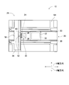
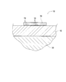
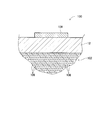
- FIG. 1 It is a figure which shows the printing apparatus which is an Example of this invention. It is sectional drawing which shows the coating film heated by the electromagnetic wave irradiation to the electromagnetic wave absorber contained in the lower part of a coating film. It is sectional drawing which shows the coating film heated by irradiation of the electromagnetic wave to the electromagnetic wave absorber contained between a coating film and a circuit board. It is sectional drawing which shows the coating film heated by irradiation of the electromagnetic wave to the electromagnetic wave absorber contained in a circuit board. It is sectional drawing which shows the coating film heated by irradiation of the electromagnetic wave to the electromagnetic wave absorber contained in a board
- maintenance apparatus It is a figure which shows the printing apparatus which is an Example of this invention. It is sectional drawing which shows the coating film heated by the electromagnetic wave irradiation to the electromagnetic wave absorber contained in the lower part of a coating film. It is sectional drawing which shows the coating film heated by irradiation of the electromagnetic wave to the electromagnetic wave absorber contained between
- FIG. 1 shows a printing apparatus 10 according to an embodiment of the present invention.
- the printing apparatus 10 is an apparatus for printing a circuit pattern on the circuit board 12.
- the printing apparatus 10 includes a transport device 20, a discharge head 22, an irradiation device 24, and a discharge head moving device (hereinafter, sometimes abbreviated as “moving device”) 26.
- the conveyance device 20 includes a pair of conveyor belts 30 extending in the X-axis direction and an electromagnetic motor (not shown) that rotates the conveyor belt 30.
- the circuit board 12 is supported by the pair of conveyor belts 30 and is conveyed in the X-axis direction by driving an electromagnetic motor.
- the transfer device 20 has a substrate holding device 32.
- the substrate holding device 32 is disposed between the pair of conveyor belts 30 and holds the circuit board 12 supported by the conveyor belts 30 in a fixed manner.
- the ejection head 22 is an inkjet type ejection head, and ejects conductive ink, specifically, a silver nanoparticle paste.
- the surface of silver nanoparticles is coated with a dispersant, and the silver nanoparticles are dispersed in a solvent.
- the ejection head 22 that ejects the silver nanoparticle paste has a head body 36 and an ejection nozzle 38.
- the discharge nozzle 38 is attached to the lower end of the head body 36, and the discharge nozzle 38 has a plurality of nozzle holes (not shown) for discharging the silver nanoparticle paste.
- the silver nanoparticle paste is ejected from the nozzle hole using a piezoelectric element (not shown) or a vapor bubble caused by heat as a drive source.
- the irradiation device 24 is a device that radiates electromagnetic waves, specifically, electromagnetic waves having a relatively high frequency of several MHz to several hundred GHz, and is attached to the lower end of the head body 36 of the ejection head 22. As a result, electromagnetic waves are emitted from above the circuit board 12 toward the circuit board 12.
- the moving device 26 includes an X-axis direction slide mechanism 50 and a Y-axis direction slide mechanism 52.
- the X-axis direction slide mechanism 50 has an X-axis slider 56 provided on the base 54 so as to be movable in the X-axis direction.
- the X-axis slider 56 moves to an arbitrary position in the X-axis direction by driving an electromagnetic motor (not shown).
- the Y-axis direction slide mechanism 52 has a Y-axis slider 60 provided on the side surface of the X-axis slider 56 so as to be movable in the Y-axis direction.
- the Y-axis slider 60 moves to an arbitrary position in the Y-axis direction by driving an electromagnetic motor (not shown).
- a head main body 36 of the ejection head 22 is attached to the Y-axis slider 60. With such a structure, the discharge nozzle 38 and the irradiation device 24 are moved to arbitrary positions on the base 54 by the moving device 26.
- a silver nanoparticle paste coating film is formed on the upper surface of the circuit board 12 by discharging the silver nanoparticle paste. Then, by heating the coating film of the silver nanoparticle paste, the silver nanoparticles are fused, and the circuit pattern is printed on the circuit board 12. Specifically, first, the circuit board 12 is transported to the working position by a command from a control device (not shown) that controls the operation of the printing apparatus 10, and the circuit board 12 is fixed by the board holding device 32 at that position. Retained.
- the ejection head 22 moves above the circuit board 12 by the operation of the moving device 26. Subsequently, the silver nanoparticle paste is discharged from the discharge nozzle 38 onto the upper surface of the circuit board 12. Thereby, as shown in FIG. 2, a coating film 70 of the silver nanoparticle paste is formed on the upper surface of the circuit board 12.
- a particulate electromagnetic wave absorber 72 is dispersed in a solvent together with silver nanoparticles.
- the electromagnetic wave absorber 72 is formed of a material that easily absorbs electromagnetic waves, for example, copper oxide, silver oxide, nickel oxide, carbon black, carbon nanotube, carbon fullerene, and the like. It is larger than the diameter.
- the silver nanoparticles have a particle size of several nm to several hundred nm, and the electromagnetic wave absorber 72 has a particle size of 0.5 ⁇ m to 5 ⁇ m. For this reason, the electromagnetic wave absorbing material 72 settles inside the coating film 70 and is positioned below the coating film 70 as shown in FIG.
- the electromagnetic wave is irradiated by the irradiation device 24 toward the coating film 70.
- the irradiated electromagnetic wave is absorbed by the electromagnetic wave absorber 72 that has settled in the coating film 70, and heats the coating film 70 from below. That is, the surface of the coating film 70 that is in contact with the circuit board 12 is heated.
- the solvent of the silver nanoparticle paste which comprises the coating film 70 evaporates sequentially from the surface of the coating film 70 on the side in contact with the circuit board 12.
- the dispersant coated on the surface of the silver nanoparticles is sequentially decomposed from the surface of the coating film 70 on the side in contact with the circuit board 12, and the plurality of silver nanoparticles are fused to each other.
- silver nanoparticles are diffused into the circuit board 12 on the surface of the coating film 70 on the side in contact with the circuit board 12.
- the circuit pattern is printed on the circuit board 12. That is, the silver nanoparticles in contact with the circuit board 12 are diffused into the circuit board 12, and the silver nanoparticles are fused on the entire coating film 70, whereby the circuit pattern is printed on the circuit board 12.
- the coating film 70 is heated from the surface on the side in contact with the circuit board 12, the silver nanoparticles in contact with the circuit board 12 diffuse into the circuit board 12, and the silver nanoparticles are The film 70 is fused from below to above.
- the coating film of the silver nanoparticle paste formed on the upper surface of the circuit board is heated by an electric furnace or the like.
- the solvent is evaporated, the dispersant is decomposed, and the silver nanoparticles are fused on the surface of the coating film. Evaporation, decomposition of the dispersing agent, and fusion of the silver nanoparticles proceed toward the inside of the coating film 70.
- the coating film is covered with the fused silver nanoparticles, and oxygen does not easily enter the coating film. Since oxygen is necessary for the decomposition of the dispersant, the dispersant may not be properly decomposed inside the coating film. In such a case, the remaining dispersant inhibits the fusion of the silver nanoparticles, and there is a possibility that a dense metal film, that is, a circuit pattern cannot be formed.
- the electromagnetic wave absorbing material 72 has settled in the coating film 70, and the electromagnetic wave absorbing material 72 is irradiated with electromagnetic waves, whereby the coating film 70. Is heated from the surface in contact with the circuit board 12.
- the evaporation of the solvent, the decomposition of the dispersant, and the fusion of the silver nanoparticles proceed from the lower side to the upper side of the coating film 70, so that the fusion of the silver nanoparticles is not hindered, and the dense metal film Is formed.
- the coating film 70 when the coating film 70 is heated from the surface on the side in contact with the circuit board 12, the silver nanoparticles in contact with the circuit board 12 are efficiently diffused into the circuit board 12. Thereby, the adhesiveness between the metal film made of silver nanoparticles and the circuit board 12 can be increased.
- the coating film is heated by an electric furnace or the like, the entire circuit board 12 is heated.
- the electromagnetic wave absorber 72 settled on the coating film 70 is heated. That is, in the printing apparatus 10, only the part to be heated is heated, and it is possible to increase the energy efficiency at the time of forming the metal film. As a result, it is possible to suppress the energy required for heating and shorten the time required for heating, thereby realizing high throughput, low cost, and the like.
- the coating film 70 is heated from the bottom by irradiating electromagnetic waves to the electromagnetic wave absorber 72 settled in the coating film 70, if it is a position which can heat a coating film from the bottom, It is possible to arrange the electromagnetic wave absorbing material in various places.
- a printing apparatus in which an electromagnetic wave absorbing material is disposed between the coating film and the circuit board and the coating film is heated by the electromagnetic wave absorbing material is shown in FIG.
- the printing apparatus 80 has the same configuration as that of the printing apparatus 10 except for the silver nanoparticle paste coating film and the electromagnetic wave absorbing material. Therefore, the same reference numerals are used for components having the same functions as the printing apparatus 10. The description will be omitted or simplified.
- a solution 84 containing an electromagnetic wave absorbing material 82 is applied on the circuit board 12 held by the board holding device 32.
- the electromagnetic wave absorbing material 82 is formed of the same material as the electromagnetic wave absorbing material 72, but the particle size thereof may not be larger than the particle size of the silver nanoparticles.
- the application of the solution 84 can be performed by various methods such as mask printing using a mask and a squeegee, and discharging the solution 84 using a discharge head or the like.
- the silver nanoparticle paste is ejected by the ejection head 22 onto the solution 84 applied on the circuit board 12. Thereby, a coating film 86 of the silver nanoparticle paste is formed on the solution 84.
- the electromagnetic wave absorber is not disperse
- the irradiation device 24 irradiates electromagnetic waves toward the coating film 86.
- the irradiated electromagnetic wave is absorbed by the electromagnetic wave absorbing material 82 contained in the solution 84 and heats the coating film 86 from below.
- the evaporation of the solvent, the decomposition of the dispersing agent, and the fusion of the silver nanoparticles proceed from the bottom to the top of the coating film 86 in the same manner as in the above-described embodiment. The same effect can be obtained.
- an electromagnetic wave absorbing material may be disposed in a circuit board, and the coating film of the silver nanoparticle paste may be heated by the electromagnetic wave absorbing material.
- a printing apparatus in which a coating film of silver nanoparticle paste is formed on a circuit board including an electromagnetic wave absorbing material and the coating film is heated by the electromagnetic wave absorbing material is referred to as a printing apparatus 90 of Modification 2 as shown in FIG. Shown in Since the printing apparatus 90 has the same configuration as that of the printing apparatus 10 except for the circuit board, the same reference numerals are used for the components having the same functions as those of the printing apparatus 10 and description thereof is omitted or simplified.
- an electromagnetic wave absorbing material 96 is contained in the circuit board 92 as shown in FIG. Then, the silver nanoparticle paste is ejected by the ejection head 22 on the circuit substrate 92, thereby forming a coating film 98 of the silver nanoparticle paste.
- the electromagnetic wave absorber is not disperse
- the irradiation device 24 irradiates electromagnetic waves toward the coating film 98.
- the irradiated electromagnetic wave is absorbed by the electromagnetic wave absorbing material 96 included in the circuit board 92 and heats the coating film 98 from below.
- the coating film 98 similarly to the coating film 70, the evaporation of the solvent, the decomposition of the dispersant, and the fusion of the silver nanoparticles proceed from the bottom to the top of the coating film 98. The same effect can be obtained.
- an electromagnetic wave absorbing material may be disposed in a substrate holding device for holding a circuit board, and the coating film of the silver nanoparticle paste may be heated by the electromagnetic wave absorbing material.
- the circuit board is held by a substrate holding device containing an electromagnetic wave absorber, and the silver nanoparticle paste coating film formed on the circuit board is heated by the electromagnetic wave absorber contained in the substrate holding device.
- the apparatus is shown in FIG. 5 as a printing apparatus 100 according to the third modification. Since the printing apparatus 100 has the same configuration as the printing apparatus 10 except for the substrate holding apparatus, the same reference numerals are used for the components having the same functions as the printing apparatus 10 and the description thereof is omitted or simplified. .
- the substrate holding device 102 contains the electromagnetic wave absorbing material 106, and the circuit board 12 is held by the substrate holding device 102. Then, a silver nanoparticle paste coating film 108 is formed on the circuit board 12 by discharging the silver nanoparticle paste by the discharge head 22. In addition, although silver nanoparticle is disperse
- the coating film 108 When the coating film 108 is formed on the circuit board 12, electromagnetic waves are irradiated by the irradiation device 24 toward the coating film 108.
- the irradiated electromagnetic wave is absorbed by the electromagnetic wave absorber 106 included in the substrate holding device 102 and heats the circuit board 12.
- the coated substrate 108 is heated from the surface on the side in contact with the circuit substrate 12 by the heated circuit substrate 12. That is, the coating film 108 is heated from below through the circuit board 12 by irradiation with electromagnetic waves.
- the evaporation of the solvent, the decomposition of the dispersing agent, and the fusion of the silver nanoparticles proceed from the bottom to the top of the coating film 108, as in the above-described coating film 70. The same effect can be obtained.
- the printing apparatus 10 is an example of a printing apparatus.
- the circuit boards 12 and 92 are examples of print media.
- the ejection head 22 is an example of an ejection head.
- the irradiation device 24 is an example of an electromagnetic wave irradiation device.
- the moving device 26 is an example of a moving device.
- the substrate holding devices 32 and 102 are an example of a stage.
- the coating films 70, 86, 98, and 108 are examples of coating films.
- the electromagnetic wave absorbers 72, 82, 96, and 106 are examples of the electromagnetic wave absorber.
- the silver nanoparticle paste is an example of a particle dispersion, and the silver nanoparticles are an example of metal particles.
- the method for forming a metal film using silver nanoparticles in the above-described embodiments and modifications is an example of a metal film forming method.
- the step of discharging the silver nanoparticle paste onto the circuit boards 12 and 92 by the discharge head 22 to form the coating films 70, 86, 98, and 108 of the silver nanoparticle paste is an example of the coating film forming step.
- the process of heating the coating films 70, 86, 98, 108 is an example of the heating process.
- the process of applying the solution 84 on the circuit board 12 is an example of the application process.
Landscapes
- Engineering & Computer Science (AREA)
- Manufacturing & Machinery (AREA)
- Microelectronics & Electronic Packaging (AREA)
- Manufacturing Of Printed Wiring (AREA)
- Application Of Or Painting With Fluid Materials (AREA)
- Other Surface Treatments For Metallic Materials (AREA)
- Coating Apparatus (AREA)
Abstract
回路基板12を支持する基板保持装置32と、金属粒子が溶剤中に分散された粒子分散液を吐出する吐出ヘッドとを備えた印刷装置10によって、回路基板上に金属膜を形成する金属膜形成方法において、吐出ヘッドにより粒子分散液を吐出することで、粒子分散液の塗膜70を回路基板上に形成し、回路基板と塗膜との間,基板保持装置,回路基板,塗膜の下部,の少なくとも1つに含まれる電磁波吸収材72に電磁波を照射することで、塗膜を回路基板に接する側の面から加熱する。これにより、溶剤の蒸発等が、塗膜の下方から上方に向かって進行するため、金属粒子の融着は阻害されず、緻密な金属膜が形成される。また、塗膜が回路基板に接する側の面から加熱されることで、金属粒子が効率的に回路基板の内部に拡散する。これにより、金属膜と回路基板との密着性が高くなる。
Description
本発明は、印刷装置を用いて印刷媒体上に金属膜を形成する金属膜形成方法および、印刷装置に関するものである。
印刷媒体上に金属膜を形成するための印刷装置は、印刷媒体を支持するステージと、金属粒子の分散された粒子分散液を吐出する吐出ヘッドとを備えている。その装置では、まず、粒子分散液が吐出ヘッドによって印刷媒体に吐出されることで、粒子分散液の塗膜が形成される。そして、その塗膜が加熱されることで、印刷媒体上に金属膜が形成される。下記特許文献に記載の印刷装置では、電磁波の照射により、粒子分散液の塗膜の加熱が行われている。
金属粒子の分散された粒子分散液では、金属粒子の分散性を向上させるべく、金属粒子の表面に分散剤がコーティングされている。このため、粒子分散液の塗膜の加熱時には、まず、溶剤が蒸発し、その後に、分散剤が分解される。そして、複数の金属粒子が融着することで、金属膜が形成される。
上記特許文献に記載の印刷装置では、電磁波の照射により粒子分散液の塗膜の加熱が行われており、塗膜の内部の温度が急激に上昇する。このため、塗膜内において、溶剤の蒸発と分散剤の分解とが同時に進行し、分散剤が変質する虞がある。その変質した分散剤は、塗膜内に残留し、金属粒子の融着を阻害するため、緻密な金属膜が形成できない虞がある。
また、温風等により、粒子分散液の塗膜の加熱が行われる場合には、塗膜の表面から内部に向かって、溶剤の蒸発、分散剤の分解、および金属粒子の融着が進行する。このため、まず、塗膜の表面で金属粒子の融着が行われる。これにより、塗膜表面で融着した金属粒子によって、塗膜の内部に酸素が進入し難くなる。酸素は、分散剤の分解に必要であるため、表面が融着した金属粒子によって覆われた塗膜の内部では、分散剤の分解が適切に行われない場合がある。このような場合には、残留した分散剤によって、金属粒子の融着が阻害され、緻密な金属膜が形成できない虞がある。
本発明は、そのような実情に鑑みてなされたものであり、粒子分散液の塗膜を適切に加熱し、緻密な金属膜を形成することが可能な印刷装置および、その印刷装置を用いた金属膜形成方法の提供を課題とする。
上記課題を解決するために、本願の請求項1に記載の金属膜形成方法は、印刷媒体を支持するステージと、金属粒子が溶剤中に分散された粒子分散液を、前記ステージに支持された前記印刷媒体に吐出する吐出ヘッドとを備えた印刷装置を用いて、前記印刷媒体上に金属膜を形成する金属膜形成方法であって、前記ステージに支持された前記印刷媒体に、前記吐出ヘッドによって前記粒子分散液を吐出することで、前記粒子分散液の塗膜を形成する塗膜形成工程と、前記塗膜形成工程において形成された前記塗膜を加熱する加熱工程とを含み、前記加熱工程が、前記印刷媒体と前記塗膜との間,前記ステージ,前記印刷媒体,前記塗膜の下部,の少なくとも1つに含まれる電磁波吸収材に電磁波を照射することで、前記塗膜の前記印刷媒体に接する側の面から加熱する工程である。
また、請求項2に記載の金属膜形成方法では、請求項1に記載の金属膜形成方法において、前記粒子分散液が、金属粒子とともに、前記電磁波吸収材が溶剤中に分散されたものであり、前記加熱工程が、前記塗膜の下部に沈降した前記電磁波吸収材に電磁波を照射することで、前記塗膜の前記印刷媒体に接する側の面から加熱する工程である。
また、請求項3に記載の金属膜形成方法は、請求項1に記載の金属膜形成方法において、前記電磁波吸収材を含む溶液を、前記ステージに支持された前記印刷媒体に塗布する塗布工程を含み、前記塗膜形成工程が、前記塗布工程において塗布された前記溶液の上に前記塗膜を形成する工程であり、前記塗布工程において塗布された前記溶液が、前記印刷媒体と前記塗膜との間とに含まれる前記電磁波吸収材として機能する。
また、請求項4に記載の金属膜形成方法では、請求項1に記載の金属膜形成方法において、前記加熱工程が、前記ステージに含まれる電磁波吸収材に電磁波を照射することで、前記印刷媒体を介して、前記塗膜の前記印刷媒体に接する側の面から加熱する工程である。
また、請求項5に記載の金属膜形成方法では、請求項1に記載の金属膜形成方法において、前記加熱工程が、前記印刷媒体に含まれる電磁波吸収材に電磁波を照射することで、前記塗膜の前記印刷媒体に接する側の面から加熱する工程である。
また、請求項6に記載の印刷装置は、印刷媒体を支持するステージと、金属粒子が溶剤中に分散された粒子分散液を、前記ステージに支持された前記印刷媒体に吐出する吐出ヘッドと、その吐出ヘッドを前記ステージ上の任意の位置に移動させる移動装置とを備えた印刷装置であって、前記吐出ヘッドが、前記ステージに支持された前記印刷媒体に、前記粒子分散液を吐出することで、前記粒子分散液の塗膜を形成し、当該印刷装置が、前記印刷媒体と前記塗膜との間,前記ステージ,前記印刷媒体,前記塗膜の下部,の少なくとも1つに含まれる電磁波吸収材に電磁波を照射することで、前記塗膜の前記印刷媒体に接する側の面から加熱する電磁波照射装置を備える。
また、請求項7に記載の印刷装置では、請求項6に記載の印刷装置において、前記電磁波照射装置が、前記吐出ヘッドに固定的に連結され、その吐出ヘッドと共に、前記移動装置によって任意の位置に移動可能とされたことを特徴とする。
請求項1に記載の金属膜形成方法および、請求項6に記載の印刷装置では、印刷媒体と塗膜との間,ステージ,印刷媒体,塗膜の下部,の少なくとも1つに含まれる電磁波吸収材に電磁波を照射することで、塗膜が印刷媒体に接する側の面から加熱される。これにより、溶剤の蒸発、分散剤の分解、および銀ナノ粒子の融着が、塗膜の下方から上方に向かって進行するため、銀ナノ粒子の融着は阻害されず、緻密な金属膜が形成される。また、塗膜が印刷媒体に接する側の面から加熱されることで、印刷媒体に接する金属粒子が効率的に印刷媒体の内部に拡散する。これにより、金属粒子による金属膜と印刷媒体との密着性を高くすることが可能となる。
また、請求項2に記載の金属膜形成方法では、粒子分散液に、金属粒子とともに、電磁波吸収材が分散されている。そして、塗膜の下部に沈降した電磁波吸収材に電磁波が照射されることで、塗膜が印刷媒体に接する側の面から加熱される。これにより、塗膜を印刷媒体に接する側の面から、好適に加熱することが可能となる。また、請求項2に記載の金属膜形成方法では、塗膜に沈降している電磁波吸収材のみが加熱される。つまり、加熱したい個所だけが加熱されており、金属膜形成時のエネルギー効率を高くすることが可能となる。これにより、加熱に要するエネルギーの抑制および、加熱に要する時間の短縮を図ることが可能となり、高スループット化,低コスト化等を実現することが可能となる。
また、請求項3に記載の金属膜形成方法では、電磁波吸収材を含む溶液が、印刷媒体に塗布され、その塗布された溶液の上に塗膜が形成される。つまり、印刷媒体と塗膜との間に、電磁波吸収材が介挿される。これにより、塗膜を印刷媒体に接する側の面から、好適に加熱することが可能となる。
また、請求項4に記載の金属膜形成方法では、ステージに電磁波吸収材が含まれている。そして、その電磁波吸収材に電磁波が照射されることで、印刷媒体を介して、塗膜が印刷媒体に接する側の面から加熱される。つまり、粒子分散液に電磁波吸収材を分散させる作業、若しくは、電磁波吸収材を含む溶液の印刷媒体への塗布作業等を行うことなく、塗膜を印刷媒体に接する側の面から加熱することが可能となる。したがって、請求項4に記載の金属膜形成方法によれば、比較的に簡便な方法で、緻密な金属膜を形成することが可能となる。
また、請求項5に記載の金属膜形成方法では、印刷媒体に電磁波吸収材が含まれている。そして、その電磁波吸収材に電磁波が照射されることで、塗膜が印刷媒体に接する側の面から加熱される。これにより、請求項4に記載の金属膜形成方法と同様に、比較的に簡便な方法で、緻密な金属膜を形成することが可能となる。
また、請求項7に記載の印刷装置では、電磁波照射装置が、吐出ヘッドに固定的に連結され、その吐出ヘッドと共に、移動装置によって任意の位置に移動する。これにより、電磁波照射装置を移動させるための専用の装置を設ける必要が無くなる。また、吐出された粒子分散液に電磁波を照射する際に、電磁波照射装置を殆ど移動させる必要が無いため、高スループット化を図ることが可能となる。
以下、本発明を実施するための形態として、本発明の実施例および変形例を、図を参照しつつ詳しく説明する。なお、本発明は、以下の実施例および変形例に限定されるものではなく、当業者の知識に基づいて種々の変更、改良を施した種々の態様で実施することができる。
<印刷装置の構成>
図1に、本発明の実施例の印刷装置10を示す。印刷装置10は、回路基板12に回路パターンを印刷するための装置である。印刷装置10は、搬送装置20と吐出ヘッド22と照射装置24と吐出ヘッド移動装置(以下、「移動装置」と略す場合がある)26とを備えている。
図1に、本発明の実施例の印刷装置10を示す。印刷装置10は、回路基板12に回路パターンを印刷するための装置である。印刷装置10は、搬送装置20と吐出ヘッド22と照射装置24と吐出ヘッド移動装置(以下、「移動装置」と略す場合がある)26とを備えている。
搬送装置20は、X軸方向に延びる1対のコンベアベルト30と、コンベアベルト30を周回させる電磁モータ(図示省略)とを有している。回路基板12は、それら1対のコンベアベルト30によって支持され、電磁モータの駆動により、X軸方向に搬送される。また、搬送装置20は、基板保持装置32を有している。基板保持装置32は、1対のコンベアベルト30の間に配設されており、コンベアベルト30によって支持された回路基板12を固定的に保持する。
吐出ヘッド22は、インクジェット方式の吐出ヘッドとされており、導電性インク、具体的には、銀ナノ粒子ペーストを吐出する。銀ナノ粒子ペーストは、銀ナノ粒子の表面に分散剤がコーティングされており、その銀ナノ粒子が溶剤中に分散されたものである。その銀ナノ粒子ペーストを吐出する吐出ヘッド22は、ヘッド本体36と吐出ノズル38とを有している。吐出ノズル38は、ヘッド本体36の下端部に装着されており、吐出ノズル38には、銀ナノ粒子ペーストを吐出するための複数のノズル穴(図示省略)が形成されている。そして、電気信号に従って、圧電素子(図示省略)や熱による蒸気泡を駆動源として、銀ナノ粒子ペーストがノズル穴から吐出される。
照射装置24は、電磁波、詳しくは、数MHzから数百GHzの比較的高周波の電磁波を照射する装置であり、吐出ヘッド22のヘッド本体36の下端部に装着されている。これにより、電磁波が、回路基板12の上方から回路基板12に向かって照射される。
移動装置26は、X軸方向スライド機構50とY軸方向スライド機構52とによって構成されている。X軸方向スライド機構50は、X軸方向に移動可能にベース54上に設けられたX軸スライダ56を有している。そのX軸スライダ56は、電磁モータ(図示省略)の駆動により、X軸方向の任意の位置に移動する。また、Y軸方向スライド機構52は、Y軸方向に移動可能にX軸スライダ56の側面に設けられたY軸スライダ60を有している。そのY軸スライダ60は、電磁モータ(図示省略)の駆動により、Y軸方向の任意の位置に移動する。そのY軸スライダ60には、吐出ヘッド22のヘッド本体36が取り付けられている。このような構造により、吐出ノズル38および照射装置24は、移動装置26によってベース54上の任意の位置に移動する。
<印刷装置の作動>
上述した構成により、印刷装置10では、回路基板12の上面に、銀ナノ粒子ペーストが吐出されることで、銀ナノ粒子ペーストの塗膜が形成される。そして、その銀ナノ粒子ペーストの塗膜が加熱されることで、銀ナノ粒子が融着し、回路パターンが回路基板12上に印刷される。具体的には、まず、印刷装置10の作動を制御する制御装置(図示省略)の指令により、回路基板12が作業位置まで搬送され、その位置において、回路基板12が、基板保持装置32によって固定的に保持される。
上述した構成により、印刷装置10では、回路基板12の上面に、銀ナノ粒子ペーストが吐出されることで、銀ナノ粒子ペーストの塗膜が形成される。そして、その銀ナノ粒子ペーストの塗膜が加熱されることで、銀ナノ粒子が融着し、回路パターンが回路基板12上に印刷される。具体的には、まず、印刷装置10の作動を制御する制御装置(図示省略)の指令により、回路基板12が作業位置まで搬送され、その位置において、回路基板12が、基板保持装置32によって固定的に保持される。
そして、吐出ヘッド22が、移動装置26の作動により回路基板12の上方に移動する。続いて、吐出ノズル38から、回路基板12の上面に銀ナノ粒子ペーストが吐出される。これにより、図2に示すように、銀ナノ粒子ペーストの塗膜70が、回路基板12の上面に形成される。
銀ナノ粒子ペーストには、銀ナノ粒子とともに、粒子状の電磁波吸収材72が溶剤中に分散されている。電磁波吸収材72は、電磁波を吸収し易い材料、例えば、酸化銅,酸化銀,酸化ニッケル,カーボンブラック,カーボンナノチューブ,カーボンフラーレン等により成形されており、それの粒径は、銀ナノ粒子の粒径より大きくされている。具体的には、銀ナノ粒子の粒径は、数nm~数百nmであり、電磁波吸収材72の粒径は、0.5μm~5μmである。このため、電磁波吸収材72は、図2に示すように、塗膜70の内部で沈降し、塗膜70の下部に位置する。
そして、その塗膜70に向かって、電磁波が、照射装置24によって照射される。照射された電磁波は、塗膜70内に沈降している電磁波吸収材72に吸収され、塗膜70を下方から加熱する。つまり、塗膜70の回路基板12に接する側の面から加熱する。これにより、塗膜70を構成する銀ナノ粒子ペーストの溶剤が、塗膜70の回路基板12に接する側の面から順次、蒸発する。そして、塗膜70の回路基板12に接する側の面から順次、銀ナノ粒子の表面にコーティングされた分散剤が分解され、複数の銀ナノ粒子が互いに融着する。この際、塗膜70の回路基板12に接する側の面では、銀ナノ粒子が回路基板12内に拡散する。そして、溶剤の蒸発、分散剤の分解、および銀ナノ粒子の融着が、塗膜70の上面にまで進行すると、回路パターンが回路基板12上に印刷される。つまり、回路基板12に接する銀ナノ粒子が回路基板12内に拡散し、銀ナノ粒子が、塗膜70全体で融着することで、回路パターンが回路基板12上に印刷される。
このように、印刷装置10では、塗膜70が回路基板12に接する側の面から加熱されることで、回路基板12に接する銀ナノ粒子が回路基板12内に拡散し、銀ナノ粒子が、塗膜70の下方から上方に向かって融着する。一方で、従来の印刷装置では、回路基板の上面に形成された銀ナノ粒子ペーストの塗膜は、電気炉等により加熱されていた。電気炉等を用いて銀ナノ粒子ペーストの塗膜が加熱される際には、まず、塗膜の表面において、溶剤の蒸発、分散剤の分解、および銀ナノ粒子の融着が行われ、溶剤の蒸発、分散剤の分解、および銀ナノ粒子の融着が、塗膜70の内部に向かって進行する。
しかし、塗膜の表面において、銀ナノ粒子の融着が行われると、その融着した銀ナノ粒子によって、塗膜が覆われ、塗膜の内部に酸素が進入し難くなる。酸素は、分散剤の分解に必要であるため、塗膜内部での分散剤の分解が適切に行われない場合がある。このような場合には、残留した分散剤によって、銀ナノ粒子の融着が阻害され、緻密な金属膜、つまり、回路パターンが形成できない虞がある。
このようなことに鑑みて、印刷装置10では、上述したように、塗膜70内に電磁波吸収材72が沈降しており、その電磁波吸収材72に電磁波が照射されることで、塗膜70が、回路基板12に接する側の面から加熱されている。これにより、溶剤の蒸発、分散剤の分解、および銀ナノ粒子の融着が、塗膜70の下方から上方に向かって進行するため、銀ナノ粒子の融着は阻害されず、緻密な金属膜が形成される。
また、塗膜70が回路基板12に接する側の面から加熱されることで、回路基板12に接する銀ナノ粒子が効率的に回路基板12内に拡散する。これにより、銀ナノ粒子による金属膜と回路基板12との密着性を高くすることが可能となる。
さらに言えば、電気炉等による塗膜の加熱時には、回路基板12全体が加熱される。一方、印刷装置10では、塗膜70に沈降している電磁波吸収材72のみが加熱される。つまり、印刷装置10では、加熱したい個所だけが加熱されており、金属膜成形時のエネルギー効率を高くすることが可能となる。これにより、加熱に要するエネルギーの抑制および、加熱に要する時間の短縮を図る可能となり、高スループット化,低コスト化等を実現することが可能となる。
<変形例1>
上記実施例では、塗膜70内に沈降した電磁波吸収材72に電磁波が照射されることで、塗膜70が下方から加熱されているが、塗膜を下方から加熱可能な位置であれば、電磁波吸収材を様々な箇所に配置させることが可能である。具体的には、塗膜と回路基板との間に電磁波吸収材を配置し、その電磁波吸収材により塗膜を加熱する印刷装置を、変形例1の印刷装置80として、図3に示す。なお、印刷装置80は、銀ナノ粒子ペーストの塗膜および電磁波吸収材を除いて、印刷装置10と同様の構成であるため、印刷装置10と同様の機能の構成要素については、同じ符号を用いて説明を省略あるいは簡略に行う。
上記実施例では、塗膜70内に沈降した電磁波吸収材72に電磁波が照射されることで、塗膜70が下方から加熱されているが、塗膜を下方から加熱可能な位置であれば、電磁波吸収材を様々な箇所に配置させることが可能である。具体的には、塗膜と回路基板との間に電磁波吸収材を配置し、その電磁波吸収材により塗膜を加熱する印刷装置を、変形例1の印刷装置80として、図3に示す。なお、印刷装置80は、銀ナノ粒子ペーストの塗膜および電磁波吸収材を除いて、印刷装置10と同様の構成であるため、印刷装置10と同様の機能の構成要素については、同じ符号を用いて説明を省略あるいは簡略に行う。
変形例1の印刷装置80では、図3に示すように、基板保持装置32に保持された回路基板12上に、電磁波吸収材82を含む溶液84が塗布される。電磁波吸収材82は、上記電磁波吸収材72と同様の素材により成形されているが、それの粒径は、銀ナノ粒子の粒径より大きくなくてもよい。なお、溶液84の塗布は、マスクとスキージとを用いたマスク印刷、吐出ヘッド等を用いた溶液84の吐出等、種々の方法により行うことが可能である。
そして、回路基板12上に塗布された溶液84の上に、銀ナノ粒子ペーストが、吐出ヘッド22によって吐出される。これにより、溶液84の上に、銀ナノ粒子ペーストの塗膜86が形成される。なお、この銀ナノ粒子ペーストには、銀ナノ粒子が分散されているが、電磁波吸収材は分散されていない。
溶液84の上に塗膜86が形成されると、その塗膜86に向かって、電磁波が、照射装置24によって照射される。照射された電磁波は、溶液84に含まれる電磁波吸収材82に吸収され、塗膜86を下方から加熱する。これにより、塗膜86でも、上記塗膜70と同様に、溶剤の蒸発、分散剤の分解、および銀ナノ粒子の融着が、塗膜86の下方から上方に向かって進行し、上記実施例と同様の効果を得ることが可能となる。
<変形例2>
上記実施例および変形例とは異なり、電磁波吸収材を回路基板内に配置させ、その電磁波吸収材により銀ナノ粒子ペーストの塗膜を加熱してもよい。具体的には、電磁波吸収材を含む回路基板上に銀ナノ粒子ペーストの塗膜を形成し、その電磁波吸収材により塗膜を加熱する印刷装置を、変形例2の印刷装置90として、図4に示す。なお、印刷装置90は、回路基板を除いて、印刷装置10と同様の構成であるため、印刷装置10と同様の機能の構成要素については、同じ符号を用いて説明を省略あるいは簡略に行う。
上記実施例および変形例とは異なり、電磁波吸収材を回路基板内に配置させ、その電磁波吸収材により銀ナノ粒子ペーストの塗膜を加熱してもよい。具体的には、電磁波吸収材を含む回路基板上に銀ナノ粒子ペーストの塗膜を形成し、その電磁波吸収材により塗膜を加熱する印刷装置を、変形例2の印刷装置90として、図4に示す。なお、印刷装置90は、回路基板を除いて、印刷装置10と同様の構成であるため、印刷装置10と同様の機能の構成要素については、同じ符号を用いて説明を省略あるいは簡略に行う。
変形例2の印刷装置90では、図4に示すように、回路基板92に電磁波吸収材96が含有されている。そして、その回路基板92の上に、銀ナノ粒子ペーストが、吐出ヘッド22によって吐出されることで、銀ナノ粒子ペーストの塗膜98が形成される。なお、この銀ナノ粒子ペーストには、銀ナノ粒子が分散されているが、電磁波吸収材は分散されていない。
回路基板92の上に塗膜98が形成されると、その塗膜98に向かって、電磁波が、照射装置24によって照射される。照射された電磁波は、回路基板92に含まれる電磁波吸収材96に吸収され、塗膜98を下方から加熱する。これにより、塗膜98でも、上記塗膜70と同様に、溶剤の蒸発、分散剤の分解、および銀ナノ粒子の融着が、塗膜98の下方から上方に向かって進行し、上記実施例と同様の効果を得ることが可能となる。
<変形例3>
上記実施例および変形例とは異なり、回路基板を保持する基板保持装置内に電磁波吸収材を配置させ、その電磁波吸収材により銀ナノ粒子ペーストの塗膜を加熱してもよい。具体的には、電磁波吸収材を含む基板保持装置によって回路基板を保持し、その回路基板上に形成された銀ナノ粒子ペーストの塗膜を、基板保持装置に含まれる電磁波吸収材により加熱する印刷装置を、変形例3の印刷装置100として、図5に示す。なお、印刷装置100は、基板保持装置を除いて、印刷装置10と同様の構成であるため、印刷装置10と同様の機能の構成要素については、同じ符号を用いて説明を省略あるいは簡略に行う。
上記実施例および変形例とは異なり、回路基板を保持する基板保持装置内に電磁波吸収材を配置させ、その電磁波吸収材により銀ナノ粒子ペーストの塗膜を加熱してもよい。具体的には、電磁波吸収材を含む基板保持装置によって回路基板を保持し、その回路基板上に形成された銀ナノ粒子ペーストの塗膜を、基板保持装置に含まれる電磁波吸収材により加熱する印刷装置を、変形例3の印刷装置100として、図5に示す。なお、印刷装置100は、基板保持装置を除いて、印刷装置10と同様の構成であるため、印刷装置10と同様の機能の構成要素については、同じ符号を用いて説明を省略あるいは簡略に行う。
変形例3の印刷装置100では、図5に示すように、基板保持装置102に電磁波吸収材106が含有されており、その基板保持装置102によって回路基板12が保持されている。そして、その回路基板12の上に、銀ナノ粒子ペーストが、吐出ヘッド22によって吐出されることで、銀ナノ粒子ペーストの塗膜108が形成される。なお、この銀ナノ粒子ペーストには、銀ナノ粒子が分散されているが、電磁波吸収材は分散されていない。
回路基板12の上に塗膜108が形成されると、その塗膜108に向かって、電磁波が、照射装置24によって照射される。照射された電磁波は、基板保持装置102に含まれる電磁波吸収材106に吸収され、回路基板12を加熱する。そして、加熱された回路基板12によって、塗膜108が回路基板12に接している側の面から加熱される。つまり、塗膜108が、電磁波の照射により、回路基板12を介して下方から加熱される。これにより、塗膜108でも、上記塗膜70と同様に、溶剤の蒸発、分散剤の分解、および銀ナノ粒子の融着が、塗膜108の下方から上方に向かって進行し、上記実施例と同様の効果を得ることが可能となる。
ちなみに、上記実施例において、印刷装置10は、印刷装置の一例である。回路基板12,92は、印刷媒体の一例である。吐出ヘッド22は、吐出ヘッドの一例である。照射装置24は、電磁波照射装置の一例である。移動装置26は、移動装置の一例である。基板保持装置32,102は、ステージの一例である。塗膜70,86,98,108は、塗膜の一例である。電磁波吸収材72,82,96,106は、電磁波吸収材の一例である。銀ナノ粒子ペーストは、粒子分散液の一例であり、銀ナノ粒子は、金属粒子の一例である。
また、上記実施例および変形例での銀ナノ粒子による金属膜の形成方法が、金属膜成形方法の一例である。吐出ヘッド22によって銀ナノ粒子ペーストを回路基板12,92の上に吐出し、銀ナノ粒子ペーストの塗膜70,86,98,108を形成する工程が、塗膜形成工程の一例である。塗膜70内に沈降した電磁波吸収材72、溶液84に含まれる電磁波吸収材82,回路基板92に含まれる電磁波吸収材96,基板保持装置102に含まれる電磁波吸収材106に電磁波を照射することで、塗膜70,86,98,108を加熱する工程が、加熱工程の一例である。回路基板12の上に溶液84を塗布する工程が、塗布工程の一例である。
10:印刷装置 12:回路基板(印刷媒体) 22:吐出ヘッド 24:照射装置(電磁波照射装置) 26:移動装置 32:基板保持装置(ステージ) 70:塗膜 72:電磁波吸収材 82:電磁波吸収材 86:塗膜 92:回路基板(印刷媒体) 96:電磁波吸収材 98:塗膜 102:基板保持装置(ステージ) 106:電磁波吸収材 108:塗膜
Claims (7)
- 印刷媒体を支持するステージと、
金属粒子が溶剤中に分散された粒子分散液を、前記ステージに支持された前記印刷媒体に吐出する吐出ヘッドと
を備えた印刷装置を用いて、前記印刷媒体上に金属膜を形成する金属膜形成方法において、
当該金属膜形成方法が、
前記ステージに支持された前記印刷媒体に、前記吐出ヘッドによって前記粒子分散液を吐出することで、前記粒子分散液の塗膜を形成する塗膜形成工程と、
前記塗膜形成工程において形成された前記塗膜を加熱する加熱工程と
を含み、
前記加熱工程が、
前記印刷媒体と前記塗膜との間,前記ステージ,前記印刷媒体,前記塗膜の下部,の少なくとも1つに含まれる電磁波吸収材に電磁波を照射することで、前記塗膜の前記印刷媒体に接する側の面から加熱する工程である金属膜形成方法。 - 前記粒子分散液が、
金属粒子とともに、前記電磁波吸収材が溶剤中に分散されたものであり、
前記加熱工程が、
前記塗膜の下部に沈降した前記電磁波吸収材に電磁波を照射することで、前記塗膜の前記印刷媒体に接する側の面から加熱する工程である請求項1に記載の金属膜形成方法。 - 当該金属膜形成方法が、
前記電磁波吸収材を含む溶液を、前記ステージに支持された前記印刷媒体に塗布する塗布工程を含み、
前記塗膜形成工程が、
前記塗布工程において塗布された前記溶液の上に前記塗膜を形成する工程であり、
前記塗布工程において塗布された前記溶液が、
前記印刷媒体と前記塗膜との間とに含まれる前記電磁波吸収材として機能する請求項1に記載の金属膜形成方法。 - 前記加熱工程が、
前記ステージに含まれる電磁波吸収材に電磁波を照射することで、前記印刷媒体を介して、前記塗膜の前記印刷媒体に接する側の面から加熱する工程である請求項1に記載の金属膜形成方法。 - 前記加熱工程が、
前記印刷媒体に含まれる電磁波吸収材に電磁波を照射することで、前記塗膜の前記印刷媒体に接する側の面から加熱する工程である請求項1に記載の金属膜形成方法。 - 印刷媒体を支持するステージと、
金属粒子が溶剤中に分散された粒子分散液を、前記ステージに支持された前記印刷媒体に吐出する吐出ヘッドと、
その吐出ヘッドを前記ステージ上の任意の位置に移動させる移動装置と
を備えた印刷装置において、
前記吐出ヘッドが、
前記ステージに支持された前記印刷媒体に、前記粒子分散液を吐出することで、前記粒子分散液の塗膜を形成し、
当該印刷装置が、
前記印刷媒体と前記塗膜との間,前記ステージ,前記印刷媒体,前記塗膜の下部,の少なくとも1つに含まれる電磁波吸収材に電磁波を照射することで、前記塗膜の前記印刷媒体に接する側の面から加熱する電磁波照射装置を備える印刷装置。 - 前記電磁波照射装置が、
前記吐出ヘッドに固定的に連結され、その吐出ヘッドと共に、前記移動装置によって任意の位置に移動可能とされた請求項6に記載の印刷装置。
Priority Applications (2)
| Application Number | Priority Date | Filing Date | Title |
|---|---|---|---|
| PCT/JP2013/050088 WO2014108995A1 (ja) | 2013-01-08 | 2013-01-08 | 金属膜形成方法、および印刷装置 |
| JP2014556237A JP6080869B2 (ja) | 2013-01-08 | 2013-01-08 | 金属膜形成方法、および印刷装置 |
Applications Claiming Priority (1)
| Application Number | Priority Date | Filing Date | Title |
|---|---|---|---|
| PCT/JP2013/050088 WO2014108995A1 (ja) | 2013-01-08 | 2013-01-08 | 金属膜形成方法、および印刷装置 |
Publications (1)
| Publication Number | Publication Date |
|---|---|
| WO2014108995A1 true WO2014108995A1 (ja) | 2014-07-17 |
Family
ID=51166672
Family Applications (1)
| Application Number | Title | Priority Date | Filing Date |
|---|---|---|---|
| PCT/JP2013/050088 Ceased WO2014108995A1 (ja) | 2013-01-08 | 2013-01-08 | 金属膜形成方法、および印刷装置 |
Country Status (2)
| Country | Link |
|---|---|
| JP (1) | JP6080869B2 (ja) |
| WO (1) | WO2014108995A1 (ja) |
Citations (3)
| Publication number | Priority date | Publication date | Assignee | Title |
|---|---|---|---|---|
| JP2009048778A (ja) * | 2007-08-13 | 2009-03-05 | Kawai Musical Instr Mfg Co Ltd | 透明導電層の形成方法及び積層構造体の形成方法 |
| WO2009044800A1 (ja) * | 2007-10-03 | 2009-04-09 | Konica Minolta Holdings, Inc. | 電極の製造方法、電子回路パターン、薄膜トランジスタ素子及び有機エレクトロルミネッセンス素子 |
| JP2009221606A (ja) * | 2008-02-26 | 2009-10-01 | Xerox Corp | 二座アミン安定化金属ナノ粒子 |
-
2013
- 2013-01-08 WO PCT/JP2013/050088 patent/WO2014108995A1/ja not_active Ceased
- 2013-01-08 JP JP2014556237A patent/JP6080869B2/ja active Active
Patent Citations (3)
| Publication number | Priority date | Publication date | Assignee | Title |
|---|---|---|---|---|
| JP2009048778A (ja) * | 2007-08-13 | 2009-03-05 | Kawai Musical Instr Mfg Co Ltd | 透明導電層の形成方法及び積層構造体の形成方法 |
| WO2009044800A1 (ja) * | 2007-10-03 | 2009-04-09 | Konica Minolta Holdings, Inc. | 電極の製造方法、電子回路パターン、薄膜トランジスタ素子及び有機エレクトロルミネッセンス素子 |
| JP2009221606A (ja) * | 2008-02-26 | 2009-10-01 | Xerox Corp | 二座アミン安定化金属ナノ粒子 |
Also Published As
| Publication number | Publication date |
|---|---|
| JP6080869B2 (ja) | 2017-02-15 |
| JPWO2014108995A1 (ja) | 2017-01-19 |
Similar Documents
| Publication | Publication Date | Title |
|---|---|---|
| JP5408878B2 (ja) | ナノ材料組成物の電気的使用、めっき的使用および触媒的使用 | |
| Wünscher et al. | Localized atmospheric plasma sintering of inkjet printed silver nanoparticles | |
| US20130319327A1 (en) | In-process orientation of particles used in direct-write inks to control electrical characteristics | |
| CN109315066B (zh) | 电路形成方法 | |
| JP2005079010A (ja) | 導電膜パターンの形成方法、電気光学装置及び電子機器 | |
| JPWO2020079744A1 (ja) | 回路形成方法 | |
| KR20140090641A (ko) | 도전성 패턴 형성용 기재, 회로 기판 및 그들의 제조 방법 | |
| JP6080869B2 (ja) | 金属膜形成方法、および印刷装置 | |
| JP6441954B2 (ja) | 配線形成方法 | |
| JP5531019B2 (ja) | 薄膜表面上の物質パターンを硬化せしめる装置及び方法 | |
| JP6411539B2 (ja) | 配線形成方法 | |
| JPWO2016189577A1 (ja) | 配線形成方法 | |
| KR101511463B1 (ko) | 패턴 형성 방법 및 패턴 형성 장치 | |
| JP6818154B2 (ja) | 配線形成方法、および配線形成装置 | |
| US20050274772A1 (en) | Treating an area to increase affinity for a fluid | |
| JP2014038951A (ja) | 射出装置および射出方法 | |
| JP6816283B2 (ja) | 配線形成方法、および配線形成装置 | |
| JP2006276121A (ja) | 機能性膜パターン成膜方法、機能性膜パターン、および電子機器 | |
| JP6808050B2 (ja) | 配線形成方法、および配線形成装置 | |
| JP7665957B2 (ja) | 立体造形装置、及び立体造形物の製造方法 | |
| Reinhold et al. | Novel developments in photonic sintering of inkjet printed functional inks | |
| JP2012151394A (ja) | 射出装置およびパターン形成装置、並びに、射出方法およびパターン形成方法 | |
| JP2008192952A (ja) | 導電性パターンの形成方法および形成装置 | |
| KR20250077227A (ko) | Uv광원 일체형 잉크젯 프린터 장치 및 프린팅 방법 | |
| JP5742295B2 (ja) | 印刷装置 |
Legal Events
| Date | Code | Title | Description |
|---|---|---|---|
| 121 | Ep: the epo has been informed by wipo that ep was designated in this application |
Ref document number: 13870821 Country of ref document: EP Kind code of ref document: A1 |
|
| ENP | Entry into the national phase |
Ref document number: 2014556237 Country of ref document: JP Kind code of ref document: A |
|
| NENP | Non-entry into the national phase |
Ref country code: DE |
|
| 122 | Ep: pct application non-entry in european phase |
Ref document number: 13870821 Country of ref document: EP Kind code of ref document: A1 |