WO2014106875A1 - Iii族窒化物エピタキシャル基板およびその製造方法 - Google Patents
Iii族窒化物エピタキシャル基板およびその製造方法 Download PDFInfo
- Publication number
- WO2014106875A1 WO2014106875A1 PCT/JP2013/007012 JP2013007012W WO2014106875A1 WO 2014106875 A1 WO2014106875 A1 WO 2014106875A1 JP 2013007012 W JP2013007012 W JP 2013007012W WO 2014106875 A1 WO2014106875 A1 WO 2014106875A1
- Authority
- WO
- WIPO (PCT)
- Prior art keywords
- layer
- substrate
- iii nitride
- group iii
- composition ratio
- Prior art date
- Legal status (The legal status is an assumption and is not a legal conclusion. Google has not performed a legal analysis and makes no representation as to the accuracy of the status listed.)
- Ceased
Links
Images

Classifications
-
- C—CHEMISTRY; METALLURGY
- C23—COATING METALLIC MATERIAL; COATING MATERIAL WITH METALLIC MATERIAL; CHEMICAL SURFACE TREATMENT; DIFFUSION TREATMENT OF METALLIC MATERIAL; COATING BY VACUUM EVAPORATION, BY SPUTTERING, BY ION IMPLANTATION OR BY CHEMICAL VAPOUR DEPOSITION, IN GENERAL; INHIBITING CORROSION OF METALLIC MATERIAL OR INCRUSTATION IN GENERAL
- C23C—COATING METALLIC MATERIAL; COATING MATERIAL WITH METALLIC MATERIAL; SURFACE TREATMENT OF METALLIC MATERIAL BY DIFFUSION INTO THE SURFACE, BY CHEMICAL CONVERSION OR SUBSTITUTION; COATING BY VACUUM EVAPORATION, BY SPUTTERING, BY ION IMPLANTATION OR BY CHEMICAL VAPOUR DEPOSITION, IN GENERAL
- C23C16/00—Chemical coating by decomposition of gaseous compounds, without leaving reaction products of surface material in the coating, i.e. chemical vapour deposition [CVD] processes
- C23C16/02—Pretreatment of the material to be coated
- C23C16/0272—Deposition of sub-layers, e.g. to promote the adhesion of the main coating
-
- C—CHEMISTRY; METALLURGY
- C23—COATING METALLIC MATERIAL; COATING MATERIAL WITH METALLIC MATERIAL; CHEMICAL SURFACE TREATMENT; DIFFUSION TREATMENT OF METALLIC MATERIAL; COATING BY VACUUM EVAPORATION, BY SPUTTERING, BY ION IMPLANTATION OR BY CHEMICAL VAPOUR DEPOSITION, IN GENERAL; INHIBITING CORROSION OF METALLIC MATERIAL OR INCRUSTATION IN GENERAL
- C23C—COATING METALLIC MATERIAL; COATING MATERIAL WITH METALLIC MATERIAL; SURFACE TREATMENT OF METALLIC MATERIAL BY DIFFUSION INTO THE SURFACE, BY CHEMICAL CONVERSION OR SUBSTITUTION; COATING BY VACUUM EVAPORATION, BY SPUTTERING, BY ION IMPLANTATION OR BY CHEMICAL VAPOUR DEPOSITION, IN GENERAL
- C23C16/00—Chemical coating by decomposition of gaseous compounds, without leaving reaction products of surface material in the coating, i.e. chemical vapour deposition [CVD] processes
- C23C16/22—Chemical coating by decomposition of gaseous compounds, without leaving reaction products of surface material in the coating, i.e. chemical vapour deposition [CVD] processes characterised by the deposition of inorganic material, other than metallic material
- C23C16/30—Deposition of compounds, mixtures or solid solutions, e.g. borides, carbides, nitrides
- C23C16/301—AIII BV compounds, where A is Al, Ga, In or Tl and B is N, P, As, Sb or Bi
- C23C16/303—Nitrides
-
- C—CHEMISTRY; METALLURGY
- C23—COATING METALLIC MATERIAL; COATING MATERIAL WITH METALLIC MATERIAL; CHEMICAL SURFACE TREATMENT; DIFFUSION TREATMENT OF METALLIC MATERIAL; COATING BY VACUUM EVAPORATION, BY SPUTTERING, BY ION IMPLANTATION OR BY CHEMICAL VAPOUR DEPOSITION, IN GENERAL; INHIBITING CORROSION OF METALLIC MATERIAL OR INCRUSTATION IN GENERAL
- C23C—COATING METALLIC MATERIAL; COATING MATERIAL WITH METALLIC MATERIAL; SURFACE TREATMENT OF METALLIC MATERIAL BY DIFFUSION INTO THE SURFACE, BY CHEMICAL CONVERSION OR SUBSTITUTION; COATING BY VACUUM EVAPORATION, BY SPUTTERING, BY ION IMPLANTATION OR BY CHEMICAL VAPOUR DEPOSITION, IN GENERAL
- C23C16/00—Chemical coating by decomposition of gaseous compounds, without leaving reaction products of surface material in the coating, i.e. chemical vapour deposition [CVD] processes
- C23C16/44—Chemical coating by decomposition of gaseous compounds, without leaving reaction products of surface material in the coating, i.e. chemical vapour deposition [CVD] processes characterised by the method of coating
- C23C16/455—Chemical coating by decomposition of gaseous compounds, without leaving reaction products of surface material in the coating, i.e. chemical vapour deposition [CVD] processes characterised by the method of coating characterised by the method used for introducing gases into reaction chamber or for modifying gas flows in reaction chamber
- C23C16/45523—Pulsed gas flow or change of composition over time
-
- C—CHEMISTRY; METALLURGY
- C23—COATING METALLIC MATERIAL; COATING MATERIAL WITH METALLIC MATERIAL; CHEMICAL SURFACE TREATMENT; DIFFUSION TREATMENT OF METALLIC MATERIAL; COATING BY VACUUM EVAPORATION, BY SPUTTERING, BY ION IMPLANTATION OR BY CHEMICAL VAPOUR DEPOSITION, IN GENERAL; INHIBITING CORROSION OF METALLIC MATERIAL OR INCRUSTATION IN GENERAL
- C23C—COATING METALLIC MATERIAL; COATING MATERIAL WITH METALLIC MATERIAL; SURFACE TREATMENT OF METALLIC MATERIAL BY DIFFUSION INTO THE SURFACE, BY CHEMICAL CONVERSION OR SUBSTITUTION; COATING BY VACUUM EVAPORATION, BY SPUTTERING, BY ION IMPLANTATION OR BY CHEMICAL VAPOUR DEPOSITION, IN GENERAL
- C23C16/00—Chemical coating by decomposition of gaseous compounds, without leaving reaction products of surface material in the coating, i.e. chemical vapour deposition [CVD] processes
- C23C16/44—Chemical coating by decomposition of gaseous compounds, without leaving reaction products of surface material in the coating, i.e. chemical vapour deposition [CVD] processes characterised by the method of coating
- C23C16/455—Chemical coating by decomposition of gaseous compounds, without leaving reaction products of surface material in the coating, i.e. chemical vapour deposition [CVD] processes characterised by the method of coating characterised by the method used for introducing gases into reaction chamber or for modifying gas flows in reaction chamber
- C23C16/45523—Pulsed gas flow or change of composition over time
- C23C16/45525—Atomic layer deposition [ALD]
- C23C16/45527—Atomic layer deposition [ALD] characterized by the ALD cycle, e.g. different flows or temperatures during half-reactions, unusual pulsing sequence, use of precursor mixtures or auxiliary reactants or activations
- C23C16/45531—Atomic layer deposition [ALD] characterized by the ALD cycle, e.g. different flows or temperatures during half-reactions, unusual pulsing sequence, use of precursor mixtures or auxiliary reactants or activations specially adapted for making ternary or higher compositions
-
- C—CHEMISTRY; METALLURGY
- C23—COATING METALLIC MATERIAL; COATING MATERIAL WITH METALLIC MATERIAL; CHEMICAL SURFACE TREATMENT; DIFFUSION TREATMENT OF METALLIC MATERIAL; COATING BY VACUUM EVAPORATION, BY SPUTTERING, BY ION IMPLANTATION OR BY CHEMICAL VAPOUR DEPOSITION, IN GENERAL; INHIBITING CORROSION OF METALLIC MATERIAL OR INCRUSTATION IN GENERAL
- C23C—COATING METALLIC MATERIAL; COATING MATERIAL WITH METALLIC MATERIAL; SURFACE TREATMENT OF METALLIC MATERIAL BY DIFFUSION INTO THE SURFACE, BY CHEMICAL CONVERSION OR SUBSTITUTION; COATING BY VACUUM EVAPORATION, BY SPUTTERING, BY ION IMPLANTATION OR BY CHEMICAL VAPOUR DEPOSITION, IN GENERAL
- C23C28/00—Coating for obtaining at least two superposed coatings either by methods not provided for in a single one of groups C23C2/00 - C23C26/00 or by combinations of methods provided for in subclasses C23C and C25C or C25D
- C23C28/04—Coating for obtaining at least two superposed coatings either by methods not provided for in a single one of groups C23C2/00 - C23C26/00 or by combinations of methods provided for in subclasses C23C and C25C or C25D only coatings of inorganic non-metallic material
- C23C28/048—Coating for obtaining at least two superposed coatings either by methods not provided for in a single one of groups C23C2/00 - C23C26/00 or by combinations of methods provided for in subclasses C23C and C25C or C25D only coatings of inorganic non-metallic material with layers graded in composition or physical properties
-
- C—CHEMISTRY; METALLURGY
- C23—COATING METALLIC MATERIAL; COATING MATERIAL WITH METALLIC MATERIAL; CHEMICAL SURFACE TREATMENT; DIFFUSION TREATMENT OF METALLIC MATERIAL; COATING BY VACUUM EVAPORATION, BY SPUTTERING, BY ION IMPLANTATION OR BY CHEMICAL VAPOUR DEPOSITION, IN GENERAL; INHIBITING CORROSION OF METALLIC MATERIAL OR INCRUSTATION IN GENERAL
- C23C—COATING METALLIC MATERIAL; COATING MATERIAL WITH METALLIC MATERIAL; SURFACE TREATMENT OF METALLIC MATERIAL BY DIFFUSION INTO THE SURFACE, BY CHEMICAL CONVERSION OR SUBSTITUTION; COATING BY VACUUM EVAPORATION, BY SPUTTERING, BY ION IMPLANTATION OR BY CHEMICAL VAPOUR DEPOSITION, IN GENERAL
- C23C28/00—Coating for obtaining at least two superposed coatings either by methods not provided for in a single one of groups C23C2/00 - C23C26/00 or by combinations of methods provided for in subclasses C23C and C25C or C25D
- C23C28/40—Coatings including alternating layers following a pattern, a periodic or defined repetition
- C23C28/42—Coatings including alternating layers following a pattern, a periodic or defined repetition characterized by the composition of the alternating layers
-
- C—CHEMISTRY; METALLURGY
- C30—CRYSTAL GROWTH
- C30B—SINGLE-CRYSTAL GROWTH; UNIDIRECTIONAL SOLIDIFICATION OF EUTECTIC MATERIAL OR UNIDIRECTIONAL DEMIXING OF EUTECTOID MATERIAL; REFINING BY ZONE-MELTING OF MATERIAL; PRODUCTION OF A HOMOGENEOUS POLYCRYSTALLINE MATERIAL WITH DEFINED STRUCTURE; SINGLE CRYSTALS OR HOMOGENEOUS POLYCRYSTALLINE MATERIAL WITH DEFINED STRUCTURE; AFTER-TREATMENT OF SINGLE CRYSTALS OR A HOMOGENEOUS POLYCRYSTALLINE MATERIAL WITH DEFINED STRUCTURE; APPARATUS THEREFOR
- C30B23/00—Single-crystal growth by condensing evaporated or sublimed materials
- C30B23/02—Epitaxial-layer growth
- C30B23/025—Epitaxial-layer growth characterised by the substrate
-
- C—CHEMISTRY; METALLURGY
- C30—CRYSTAL GROWTH
- C30B—SINGLE-CRYSTAL GROWTH; UNIDIRECTIONAL SOLIDIFICATION OF EUTECTIC MATERIAL OR UNIDIRECTIONAL DEMIXING OF EUTECTOID MATERIAL; REFINING BY ZONE-MELTING OF MATERIAL; PRODUCTION OF A HOMOGENEOUS POLYCRYSTALLINE MATERIAL WITH DEFINED STRUCTURE; SINGLE CRYSTALS OR HOMOGENEOUS POLYCRYSTALLINE MATERIAL WITH DEFINED STRUCTURE; AFTER-TREATMENT OF SINGLE CRYSTALS OR A HOMOGENEOUS POLYCRYSTALLINE MATERIAL WITH DEFINED STRUCTURE; APPARATUS THEREFOR
- C30B25/00—Single-crystal growth by chemical reaction of reactive gases, e.g. chemical vapour-deposition growth
- C30B25/02—Epitaxial-layer growth
- C30B25/18—Epitaxial-layer growth characterised by the substrate
- C30B25/183—Epitaxial-layer growth characterised by the substrate being provided with a buffer layer, e.g. a lattice matching layer
-
- C—CHEMISTRY; METALLURGY
- C30—CRYSTAL GROWTH
- C30B—SINGLE-CRYSTAL GROWTH; UNIDIRECTIONAL SOLIDIFICATION OF EUTECTIC MATERIAL OR UNIDIRECTIONAL DEMIXING OF EUTECTOID MATERIAL; REFINING BY ZONE-MELTING OF MATERIAL; PRODUCTION OF A HOMOGENEOUS POLYCRYSTALLINE MATERIAL WITH DEFINED STRUCTURE; SINGLE CRYSTALS OR HOMOGENEOUS POLYCRYSTALLINE MATERIAL WITH DEFINED STRUCTURE; AFTER-TREATMENT OF SINGLE CRYSTALS OR A HOMOGENEOUS POLYCRYSTALLINE MATERIAL WITH DEFINED STRUCTURE; APPARATUS THEREFOR
- C30B29/00—Single crystals or homogeneous polycrystalline material with defined structure characterised by the material or by their shape
- C30B29/10—Inorganic compounds or compositions
- C30B29/40—AIIIBV compounds wherein A is B, Al, Ga, In or Tl and B is N, P, As, Sb or Bi
- C30B29/403—AIII-nitrides
-
- H—ELECTRICITY
- H10—SEMICONDUCTOR DEVICES; ELECTRIC SOLID-STATE DEVICES NOT OTHERWISE PROVIDED FOR
- H10D—INORGANIC ELECTRIC SEMICONDUCTOR DEVICES
- H10D30/00—Field-effect transistors [FET]
- H10D30/40—FETs having zero-dimensional [0D], one-dimensional [1D] or two-dimensional [2D] charge carrier gas channels
- H10D30/47—FETs having zero-dimensional [0D], one-dimensional [1D] or two-dimensional [2D] charge carrier gas channels having two-dimensional [2D] charge carrier gas channels, e.g. nanoribbon FETs or high electron mobility transistors [HEMT]
- H10D30/471—High electron mobility transistors [HEMT] or high hole mobility transistors [HHMT]
- H10D30/473—High electron mobility transistors [HEMT] or high hole mobility transistors [HHMT] having confinement of carriers by multiple heterojunctions, e.g. quantum well HEMT
- H10D30/4732—High electron mobility transistors [HEMT] or high hole mobility transistors [HHMT] having confinement of carriers by multiple heterojunctions, e.g. quantum well HEMT using Group III-V semiconductor material
-
- H—ELECTRICITY
- H10—SEMICONDUCTOR DEVICES; ELECTRIC SOLID-STATE DEVICES NOT OTHERWISE PROVIDED FOR
- H10D—INORGANIC ELECTRIC SEMICONDUCTOR DEVICES
- H10D62/00—Semiconductor bodies, or regions thereof, of devices having potential barriers
- H10D62/80—Semiconductor bodies, or regions thereof, of devices having potential barriers characterised by the materials
- H10D62/81—Semiconductor bodies, or regions thereof, of devices having potential barriers characterised by the materials of structures exhibiting quantum-confinement effects, e.g. single quantum wells; of structures having periodic or quasi-periodic potential variation
- H10D62/815—Semiconductor bodies, or regions thereof, of devices having potential barriers characterised by the materials of structures exhibiting quantum-confinement effects, e.g. single quantum wells; of structures having periodic or quasi-periodic potential variation of structures having periodic or quasi-periodic potential variation, e.g. superlattices or multiple quantum wells [MQW]
-
- H—ELECTRICITY
- H10—SEMICONDUCTOR DEVICES; ELECTRIC SOLID-STATE DEVICES NOT OTHERWISE PROVIDED FOR
- H10D—INORGANIC ELECTRIC SEMICONDUCTOR DEVICES
- H10D62/00—Semiconductor bodies, or regions thereof, of devices having potential barriers
- H10D62/80—Semiconductor bodies, or regions thereof, of devices having potential barriers characterised by the materials
- H10D62/81—Semiconductor bodies, or regions thereof, of devices having potential barriers characterised by the materials of structures exhibiting quantum-confinement effects, e.g. single quantum wells; of structures having periodic or quasi-periodic potential variation
- H10D62/815—Semiconductor bodies, or regions thereof, of devices having potential barriers characterised by the materials of structures exhibiting quantum-confinement effects, e.g. single quantum wells; of structures having periodic or quasi-periodic potential variation of structures having periodic or quasi-periodic potential variation, e.g. superlattices or multiple quantum wells [MQW]
- H10D62/8161—Semiconductor bodies, or regions thereof, of devices having potential barriers characterised by the materials of structures exhibiting quantum-confinement effects, e.g. single quantum wells; of structures having periodic or quasi-periodic potential variation of structures having periodic or quasi-periodic potential variation, e.g. superlattices or multiple quantum wells [MQW] potential variation due to variations in composition or crystallinity, e.g. heterojunction superlattices
- H10D62/8162—Semiconductor bodies, or regions thereof, of devices having potential barriers characterised by the materials of structures exhibiting quantum-confinement effects, e.g. single quantum wells; of structures having periodic or quasi-periodic potential variation of structures having periodic or quasi-periodic potential variation, e.g. superlattices or multiple quantum wells [MQW] potential variation due to variations in composition or crystallinity, e.g. heterojunction superlattices having quantum effects only in the vertical direction, i.e. layered structures having quantum effects solely resulting from vertical potential variation
- H10D62/8164—Semiconductor bodies, or regions thereof, of devices having potential barriers characterised by the materials of structures exhibiting quantum-confinement effects, e.g. single quantum wells; of structures having periodic or quasi-periodic potential variation of structures having periodic or quasi-periodic potential variation, e.g. superlattices or multiple quantum wells [MQW] potential variation due to variations in composition or crystallinity, e.g. heterojunction superlattices having quantum effects only in the vertical direction, i.e. layered structures having quantum effects solely resulting from vertical potential variation comprising only semiconductor materials
-
- H—ELECTRICITY
- H10—SEMICONDUCTOR DEVICES; ELECTRIC SOLID-STATE DEVICES NOT OTHERWISE PROVIDED FOR
- H10D—INORGANIC ELECTRIC SEMICONDUCTOR DEVICES
- H10D62/00—Semiconductor bodies, or regions thereof, of devices having potential barriers
- H10D62/80—Semiconductor bodies, or regions thereof, of devices having potential barriers characterised by the materials
- H10D62/85—Semiconductor bodies, or regions thereof, of devices having potential barriers characterised by the materials being Group III-V materials, e.g. GaAs
- H10D62/8503—Nitride Group III-V materials, e.g. AlN or GaN
-
- H—ELECTRICITY
- H10—SEMICONDUCTOR DEVICES; ELECTRIC SOLID-STATE DEVICES NOT OTHERWISE PROVIDED FOR
- H10P—GENERIC PROCESSES OR APPARATUS FOR THE MANUFACTURE OR TREATMENT OF DEVICES COVERED BY CLASS H10
- H10P14/00—Formation of materials, e.g. in the shape of layers or pillars
- H10P14/20—Formation of materials, e.g. in the shape of layers or pillars of semiconductor materials
- H10P14/29—Formation of materials, e.g. in the shape of layers or pillars of semiconductor materials characterised by the substrates
- H10P14/2901—Materials
- H10P14/2902—Materials being Group IVA materials
- H10P14/2905—Silicon, silicon germanium or germanium
-
- H—ELECTRICITY
- H10—SEMICONDUCTOR DEVICES; ELECTRIC SOLID-STATE DEVICES NOT OTHERWISE PROVIDED FOR
- H10P—GENERIC PROCESSES OR APPARATUS FOR THE MANUFACTURE OR TREATMENT OF DEVICES COVERED BY CLASS H10
- H10P14/00—Formation of materials, e.g. in the shape of layers or pillars
- H10P14/20—Formation of materials, e.g. in the shape of layers or pillars of semiconductor materials
- H10P14/32—Formation of materials, e.g. in the shape of layers or pillars of semiconductor materials characterised by intermediate layers between substrates and deposited layers
- H10P14/3202—Materials thereof
- H10P14/3214—Materials thereof being Group IIIA-VA semiconductors
- H10P14/3216—Nitrides
-
- H—ELECTRICITY
- H10—SEMICONDUCTOR DEVICES; ELECTRIC SOLID-STATE DEVICES NOT OTHERWISE PROVIDED FOR
- H10P—GENERIC PROCESSES OR APPARATUS FOR THE MANUFACTURE OR TREATMENT OF DEVICES COVERED BY CLASS H10
- H10P14/00—Formation of materials, e.g. in the shape of layers or pillars
- H10P14/20—Formation of materials, e.g. in the shape of layers or pillars of semiconductor materials
- H10P14/32—Formation of materials, e.g. in the shape of layers or pillars of semiconductor materials characterised by intermediate layers between substrates and deposited layers
- H10P14/3242—Structure
- H10P14/3244—Layer structure
- H10P14/3251—Layer structure consisting of three or more layers
- H10P14/3252—Alternating layers, e.g. superlattice
-
- H—ELECTRICITY
- H10—SEMICONDUCTOR DEVICES; ELECTRIC SOLID-STATE DEVICES NOT OTHERWISE PROVIDED FOR
- H10P—GENERIC PROCESSES OR APPARATUS FOR THE MANUFACTURE OR TREATMENT OF DEVICES COVERED BY CLASS H10
- H10P14/00—Formation of materials, e.g. in the shape of layers or pillars
- H10P14/20—Formation of materials, e.g. in the shape of layers or pillars of semiconductor materials
- H10P14/34—Deposited materials, e.g. layers
- H10P14/3402—Deposited materials, e.g. layers characterised by the chemical composition
- H10P14/3414—Deposited materials, e.g. layers characterised by the chemical composition being group IIIA-VIA materials
- H10P14/3416—Nitrides
-
- H—ELECTRICITY
- H10—SEMICONDUCTOR DEVICES; ELECTRIC SOLID-STATE DEVICES NOT OTHERWISE PROVIDED FOR
- H10D—INORGANIC ELECTRIC SEMICONDUCTOR DEVICES
- H10D62/00—Semiconductor bodies, or regions thereof, of devices having potential barriers
- H10D62/10—Shapes, relative sizes or dispositions of the regions of the semiconductor bodies; Shapes of the semiconductor bodies
- H10D62/17—Semiconductor regions connected to electrodes not carrying current to be rectified, amplified or switched, e.g. channel regions
- H10D62/351—Substrate regions of field-effect devices
- H10D62/357—Substrate regions of field-effect devices of FETs
Definitions
- the present invention relates to a group III nitride epitaxial substrate and a manufacturing method thereof.
- group III nitride semiconductors composed of compounds of Al, Ga, In, and the like and N have been widely used for light-emitting elements, electronic device elements, and the like. Since the characteristics of such a device are greatly influenced by the crystallinity of a group III nitride semiconductor, a technique for growing a group III nitride semiconductor having high crystallinity is required.
- the group III nitride semiconductor has been conventionally formed by epitaxial growth on a sapphire substrate.
- the sapphire substrate has a low thermal conductivity, heat dissipation is poor, and there is a problem that it is not suitable for making a high-power device.
- the Si substrate has higher heat dissipation than the sapphire substrate, it is suitable for the production of a high output device, and since the large substrate is inexpensive, it has an advantage that the manufacturing cost can be suppressed.
- the Si substrate has a lattice constant different from that of the group III nitride semiconductor. Even if the group III nitride semiconductor is grown directly on the Si substrate, the group III nitride semiconductor having high crystallinity is obtained. I could't expect to get it.
- Patent Document 1 discloses that a first layer made of Al x Ga 1-x N (0.5 ⁇ x ⁇ 1) and Al y Ga 1-y N between the Si substrate and the group III nitride semiconductor.
- a first layer made of Al x Ga 1-x N (0.5 ⁇ x ⁇ 1) and Al y Ga 1-y N between the Si substrate and the group III nitride semiconductor.
- Patent Document 1 refers to preventing the occurrence of cracks in the group III nitride semiconductor layer (main laminate) thereon by forming a nitride semiconductor superlattice structure.
- a conventional superlattice laminate as in Patent Document 1 is formed on a Si substrate, and a main laminate composed of a group III nitride semiconductor layer is formed thereon.
- the obtained group III nitride epitaxial substrate may be greatly warped with the Si substrate side as a concave and the main laminate side as a convex.
- the warpage of the group III nitride epitaxial substrate hereinafter, the case where the Si substrate side is warped and the main laminate side is warped as convex is referred to as “upwardly warped upward”, on the contrary, the Si substrate side is warped.
- the main laminate side warps as a convex it is referred to as “lower convexly”.
- group III nitride epitaxial substrate is also required to improve the vertical breakdown voltage.
- the present invention has an object to provide a group III nitride epitaxial substrate and a method for manufacturing the same that reduce warpage after forming a main laminate and improve longitudinal breakdown voltage.
- the group III nitride epitaxial substrate of the present invention capable of achieving this object is formed of an Si substrate, an initial layer in contact with the Si substrate, an Al ⁇ Ga 1- ⁇ N (0 a .5 ⁇ and alpha ⁇ 1 first layer consists of) and Al ⁇ Ga 1- ⁇ N ( 0 ⁇ formed by alternately stacking a second layer consisting of beta ⁇ 0.5) superlattice laminate, a
- the Al composition ratio ⁇ of the second layer gradually increases as the distance from the Si substrate increases.
- the superlattice laminate has a plurality of superlattice layers formed by alternately laminating the first layer and the second layer having a constant Al composition ratio ⁇ , and the Al composition ratio of the second layer It is preferable that ⁇ is larger in the superlattice layer at a position away from the Si substrate.
- a difference xy between the Al composition ratio x of the second layer closest to the Si substrate and the Al composition ratio y of the second layer farthest from the Si substrate is 0.02 or more.
- the first layer is preferably AlN.
- the initial layer includes an AlN layer and an Al z Ga 1-z N layer (0 ⁇ z ⁇ 1) on the AlN layer, and the Al composition ratio z of the Al z Ga 1-z N layer is: It is preferable that the Al composition ratio y of the second layer farthest from the Si substrate is larger.
- a main laminate formed by epitaxially growing a group III nitride layer including at least two layers of an AlGaN layer and a GaN layer on the superlattice laminate.
- the warpage amount after forming the main laminate is not more than the value of the following formula (1). (X / 6) 2 ⁇ 50 ⁇ m (1) Where x is the inch size of the Si substrate. That is, when the Si substrate is 6 inches, it is preferable that the warpage amount after forming the main laminate is 50 ⁇ m or less.
- the method for producing a group III nitride epitaxial substrate of the present invention includes a first step of forming an initial layer in contact with the Si substrate on the Si substrate, and Al ⁇ Ga 1- ⁇ N (0. 5 ⁇ alpha ⁇ 1 first layer consists of) and Al ⁇ Ga 1- ⁇ N ( 0 ⁇ a second step of forming a beta ⁇ 0.5) formed by alternately stacking second layer of the superlattice laminate In the second step, the Al composition ratio ⁇ of the second layer is gradually increased as the distance from the Si substrate increases.
- the Al composition ratio ⁇ of the second layer gradually increases as the distance from the Si substrate increases, thereby reducing the warp after forming the main laminate and improving the vertical breakdown voltage.
- a nitride epitaxial substrate can be obtained.
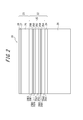
- FIG. 1 is a schematic cross-sectional view of a group III nitride epitaxial substrate 10 according to the present invention.
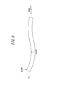
- FIG. 6 is a schematic cross-sectional view of another group III nitride epitaxial substrate 20 according to the present invention. It is a schematic cross section of the substrate for explaining the definition of the warpage amount (SORI).
- SORI warpage amount
- a group III nitride epitaxial substrate 10 includes a Si substrate 11 and a buffer layer 12 formed on the Si substrate 11 as shown in FIG.
- a main laminate 13 formed by epitaxially growing a group III nitride layer on the buffer layer 12 can be provided.
- the buffer layer 12 is formed on the initial layer 14 in contact with the Si substrate 11, and is formed on the initial layer 14.
- the buffer layer 12 includes a first layer made of Al ⁇ Ga 1- ⁇ N (0.5 ⁇ ⁇ 1) and Al ⁇ Ga 1.
- a superlattice laminate 15 in which second layers made of - ⁇ N (0 ⁇ ⁇ 0.5) are alternately laminated.
- a second superlattice layer 15B made of the second layer 15B2 consisting .85 N laminated alternately, a superlattice layer of two layers of.
- the Si substrate 11 is a Si single crystal substrate, and the plane orientation is not particularly specified, and (111), (100), (110) planes, etc. can be used, but the (0001) plane of group III nitride is used.
- the (110) and (111) planes are desirable for growth, and the (111) plane is desirably used for growth with good surface flatness.
- any of p-type and n-type conductivity may be used, and it is applicable to various resistivities from 0.001 to 100,000 ⁇ ⁇ cm.
- impurities (C, O, N, Ge, etc.) for purposes other than controlling conductivity may be included in the Si substrate.
- the thickness of the substrate is appropriately set in consideration of the amount of warpage after epitaxial growth of each layer, and is, for example, in the range of 500 to 2000 ⁇ m.
- a typical material constituting the initial layer 14 includes AlGaN or AlN.
- the substrate contact portion of the initial layer 14 an AlN layer, the reaction with the Si substrate 11 is suppressed, and the longitudinal breakdown voltage is reduced. Can be improved.
- the initial layer 14 does not necessarily have a uniform composition in the film thickness direction. If the substrate contact portion is an AlN layer, an AlGaN layer is formed on the AlN layer, and a plurality of layers having different compositions are laminated. Or a composition gradient. Further, a thin film such as a Si nitride film, an oxide film, or a carbonized film may be inserted into the interface portion between the AlN and Si single crystal substrate, or a thin film obtained by reacting such a film with AlN may be inserted.
- the initial layer 14 may be formed in an amorphous layer or a polycrystalline layer, such as a low-temperature buffer layer, with a thickness that does not impair the crystal quality.
- the thickness of the initial layer 14 is, for example, in the range of 10 to 500 nm. If it is less than 10 nm, a defect may occur due to the reaction between Ga, which is a part of the raw material of the upper layer, and the Si substrate. If it exceeds 500 nm, a crack occurs when the initial layer is formed. Because there is a possibility.
- the second layer 15A2 of the first superlattice layer 15A has an Al composition ratio ⁇ of 0.10
- the second layer 15B2 of the second superlattice layer 15B has an Al composition ratio ⁇ of 0.15.
- the characteristic is that the Al composition ratio ⁇ of the second layer increases as the distance from the Si substrate 11 increases.
- the Al composition ratio ⁇ of the AlGaN layer having a low Al composition ratio ⁇ is separated from the Si substrate.
- the inventors have found that the warpage of the group III nitride epitaxial substrate 10 after the formation of the main laminate 13 can be reduced by increasing the thickness of the main laminate 13. As a result, the possibility of device failure in the device formation process for the main laminate can be reduced.
- the superlattice laminate 15 of the present invention can cancel the stress between the main laminate 13 and reduce the warpage of the group III nitride epitaxial substrate 10 after the main laminate 13 is formed.
- the Al composition ratio ⁇ of the second layer increases as the distance from the Si substrate 11 increases, on the contrary, the Al composition ratio of the second layer decreases as the distance from the Si substrate decreases. There is also an effect that the directional breakdown voltage is improved.
- the band gap increases as the Al composition ratio increases, and the inherent resistance of the material itself increases.
- the ratio of using a layer having a high Al composition ratio for the superlattice layer increases, so that the resistance of the buffer layer can be increased, and the effect of reducing leakage current and improving breakdown voltage can be obtained.
- the compressive stress generated as a whole of the superlattice laminate becomes too large, cracks are generated, so the compositional difference needs to be set appropriately.
- the main laminate 13 is formed by epitaxially growing a group III nitride layer including at least two layers of an AlGaN layer and a GaN layer on the buffer layer 12.
- the main stacked body 13 is formed on the AlGaN layer 16 formed on the second superlattice layer 15B, the channel layer 17 made of GaN formed on the AlGaN layer 16, and the channel layer 17.
- an electron supply layer 18 made of AlGaN having a larger band gap than the channel layer.
- the GaN layer in the main laminate 13 is preferably located closest to the electron supply layer 18 as in the present embodiment.
- the layer immediately above the superlattice laminate 15 is preferably AlGaN or GaN having an Al composition ratio lower than that of the uppermost second layer in the superlattice laminate 15 so that compressive stress is applied to the layer. .
- the thickness of the main laminate 13 is preferably in the range of 0.1 to 5 ⁇ m. This is because if the thickness is less than 0.1 ⁇ m, defects such as pits may occur, and if it exceeds 5 ⁇ m, cracks may occur in the main laminate 13.
- the thicknesses of the channel layer 16 and the electron supply layer 17 may be appropriately set in device design.
- the group III nitride epitaxial substrate 10 of this embodiment can be used for any electronic device (LED, LD, transistor, diode, etc.), and is particularly preferably used for a HEMT (High Electron Mobility Transistor).
- LED light-emitting diode
- HEMT High Electron Mobility Transistor
- the step of forming the group III nitride epitaxial substrate 10 of the present invention as a device includes a step of forming an electrode on the substrate 10, a step of forming a groove by etching to separate the nitride semiconductor layer, a surface passivation film
- separating an element, etc. are mentioned, and conveyance of an element is performed between each process.
- a group III nitride epitaxial substrate 20 includes a Si substrate 21 and a buffer layer 22 formed on the Si substrate 21, as shown in FIG.
- a main laminate 23 formed by epitaxially growing a group III nitride layer on the buffer layer 22 can be provided.
- the buffer layer 22 is formed on the initial layer 24 in contact with the Si substrate 11, the first layer made of Al ⁇ Ga 1- ⁇ N (0.5 ⁇ ⁇ 1), and Al ⁇ Ga 1.
- a superlattice laminate 25 in which second layers made of - ⁇ N (0 ⁇ ⁇ 0.5) are alternately laminated.
- the first superlattice layer 25A formed by alternately stacking two layers 25A2, the first layer 25B1 ( ⁇ 1) made of, for example, AlN, and the Al 0.12 Ga 0 in which the Al composition ratio ⁇ takes a constant value 0.12.
- a second superlattice layer 25B made of the second layer 25B2 consisting .88 N by alternately stacking, for example, the first layer 25C1 consisting AlN (alpha 1) and the Al composition ratio ⁇ takes a constant value 0.14
- Al 0.16 Ga 0 take the value 0.16.
- the Al composition ratio ⁇ of the second layers 25A2 to 25E2 in the five superlattice layers 25A to 25E is 0.10 ⁇ 0.12 ⁇ 0.14 ⁇ 0.16 ⁇ 0.18, and Si As the distance from the substrate 21 increases, the warpage of the group III nitride epitaxial substrate 20 after the main laminate 23 is formed can be reduced and the vertical breakdown voltage can be improved, as in the first embodiment.
- the Si substrate 21, the initial layer 24, the AlGaN layer 26, the channel layer 27, and the electron supply layer 28 are the same as those in the first embodiment.
- the superlattice laminate 15, 25 of the first and second embodiments a plurality of superlattice layers, a first layer over the superlattice layer and AlN, first made of Al ⁇ Ga 1- ⁇ N in each superlattice layers
- the constant Al composition ratio ⁇ of the two layers is increased as the distance from the substrate increases.
- the change of the Al composition ratio in the superlattice laminate for example, the following may be used.
- the Al composition ratio ⁇ of the second layer gradually increases as the distance from the substrate increases.
- the gradual increase means increasing continuously or stepwise, and the Al composition ratio of the second layer is increased in addition to the step of increasing the Al composition ratio ⁇ of the second layer stepwise by the plurality of superlattice layers. This includes the case where the ratio ⁇ continues to increase as the distance from the Si substrate increases. Even in such a case, it is clear that the effects described in the first embodiment can be achieved.
- the second layer in the present invention has an Al composition ratio ⁇ of 0 ⁇ ⁇ 0.5
- the first layer has an Al composition ratio ⁇ of 0.5 ⁇ ⁇ 1, so Regardless of whether the layer is near or far from the device, the layer always has a lower Al composition ratio than the first layer. Therefore, in the present invention, it is not necessary to limit the first layer to the same composition (AlN in the first and second embodiments) regardless of the distance from the element, and 0.5 ⁇ ⁇ between the plurality of first layers.
- the Al composition ratio may be changed within the range of 1.
- all the first layers are AlN. This is because the difference in Al composition ratio between the adjacent second layers is maximized and the strain buffering effect is maximized.
- the second layer in the present invention is not particularly limited if the Al composition ratio ⁇ is 0 ⁇ ⁇ 0.5, but the Al composition ratio y of the second layer farthest from the Si substrate is 0.05 to 0.5. It is preferable to be within the range. If y is less than 0.05, the longitudinal breakdown voltage may not be sufficiently secured, and if it exceeds 0.5, the strain buffering effect may be insufficient and cracks may occur in the superlattice laminate. Because there is.
- the Al composition ratio x of the second layer closest to the Si substrate does not become zero. That is, the second layer does not become GaN. This is because when the second layer is made of GaN, the longitudinal breakdown voltage of the element cannot be sufficiently secured. Furthermore, when the vertical breakdown voltage is particularly important, x is preferably larger than 0.05, more preferably 0.10 or higher, from the viewpoint of securing the vertical breakdown voltage of the element.
- the relationship between the Al composition ratio x of the second layer closest to the Si substrate and the Al composition ratio y of the second layer farthest from the Si substrate is within the range of the value of the Al composition ratio ⁇ . It is preferable that x ⁇ y and the difference (y ⁇ x) is 0.02 or more. This is because if it is less than 0.02, the warp reduction effect may be insufficient. Furthermore, the difference (y ⁇ x) is preferably 0.45 or less, and more preferably 0.2 or less.
- the Al composition ratio z is the second most distant from the Si substrate. It is preferable that the layer is larger than the Al composition ratio y of the second layer having the maximum Al composition ratio in the second layer. It is because it can suppress that a crack generate
- AlGaN constituting the buffer layer may contain a total of 1% or less of other group III elements B and / or In. Further, for example, a trace amount of impurities such as Si, H, O, C, Mg, As, and P may be included. Note that GaN, AlGaN, etc. constituting the main laminate may similarly contain other group III elements in total of 1% or less.
- the thickness of a set of superlattice laminates in the present invention is appropriately set depending on the composition, and may be, for example, about 1 to 100 nm.
- the thickness of the first layer can be 0.5 to 200 nm, and the thickness of the second layer can be 0.5 to 100 nm.
- the number of sets of the superlattice laminate (first layer and second layer) in the present invention is appropriately set depending on the required breakdown voltage, and can be set to 40 to 300, for example.
- the total thickness of the superlattice laminate is preferably 1 ⁇ m or more. This is because when the thickness is 1 ⁇ m or more, the total sum of stresses generated in the film is sufficiently large, so that the effects of the present invention are sufficiently exhibited.
- the amount of warpage after the formation of the main laminate is preferably not more than the value of the following formula (1).
- x is the inch size of the Si substrate. That is, when the Si substrate is 6 inches, it is preferable that the warpage amount after forming the main laminate is 50 ⁇ m or less. Thereby, the device defect in the device formation process with respect to the main laminated body can be reduced more effectively.
- the method for producing a group III nitride epitaxial substrate of the present invention includes, for example, a first step of forming an initial layer 14 in contact with the Si substrate 11 on the Si substrate 11 as shown in FIG.
- a first layer 15A1 (15B1) made of Al ⁇ Ga 1- ⁇ N (0.5 ⁇ ⁇ 1) and a second layer 15A2 made of Al ⁇ Ga 1- ⁇ N (0 ⁇ ⁇ 0.5).
- the Al composition ratio ⁇ of the second layer is set to be higher than that of the first superlattice layer 15A.
- the second superlattice layer 15B that is, the distance from the Si substrate 11 is gradually increased.
- the main laminate 13 can be formed by epitaxially growing a group III nitride layer on the buffer layer 12.
- a known method for epitaxial growth of each layer in the present invention a known method such as MOCVD method or MBE method can be used.
- source gases for forming AlGaN include TMA (trimethylaluminum), TMG (trimethylgallium), and ammonia.
- Control of the Al composition ratio in the film controls the mixing ratio of TMA and TMG. Can be done.
- a known method such as TEM-EDS can be used for evaluation of the Al composition ratio and film thickness after epitaxial growth.
- Example 1 On a (111) plane 6-inch p-type Si single crystal substrate (B-doped, specific resistance 0.02 ⁇ ⁇ cm, thickness: 625 ⁇ m), AlN (thickness: 120 nm) and Al 0.35 Ga 0 are used as buffer layers. An initial layer was formed by sequentially stacking .65 N (thickness: 50 nm).
- a first superlattice layer in which 50 pairs of AlN (thickness: 3.5 nm) and Al 0.10 Ga 0.90 N (thickness: 25 nm) are alternately stacked on the initial layer, and AlN (thickness) : 3.5 nm) and second superlattice layers in which 50 sets of Al 0.15 Ga 0.85 N (thickness: 25 nm) were alternately laminated were sequentially epitaxially grown to obtain a superlattice laminate.
- GaN channel layer (thickness: 20 nm) Al 0.25 Ga 0.75 N electron supply layer (thickness) on the superlattice laminate.
- Group 30 nm was epitaxially grown as a main laminate to produce a group III nitride epitaxial substrate as in Embodiment 1 having a HEMT structure.
- an MOCVD method using TMA (trimethylaluminum), TMG (trimethylgallium), and ammonia as raw materials was used. Nitrogen / hydrogen was used as the carrier gas.
- the growth conditions (pressure and temperature) of each layer were 20 kPa, 1000 ° C., and the V / III ratio was 2000.
- the Al composition ratio in each AlGaN layer was controlled by appropriately controlling the mixing ratio of TMA and TMG. The same applies to each of the following examples and comparative examples.
- Example 2 First superlattice layers in which 20 sets of AlN (thickness: 3.5 nm) and Al 0.10 Ga 0.90 N (thickness: 25 nm) are alternately laminated, and AlN (thickness: 3.5 nm) and Al 0.12 Ga 0.88 N (thickness: 25 nm) alternately stacked second superlattice layers, AlN (thickness: 3.5 nm) and Al 0.14 Ga 0
- a third superlattice layer in which 20 sets of .85 N (thickness: 25 nm) are alternately stacked, AlN (thickness: 3.5 nm) and Al 0.16 Ga 0.84 N (thickness: 25 nm)
- Example 3 First superlattice layers in which 20 sets of AlN (thickness: 3.5 nm) and Al 0.10 Ga 0.90 N (thickness: 25 nm) are alternately laminated, and AlN (thickness: 3.5 nm) and Al 0.11 Ga 0.89 N (thickness: 25 nm) alternately stacked second superlattice layer, AlN (thickness: 3.5 nm) and Al 0.12 Ga 0
- a third superlattice layer in which 20 pairs of .88 N (thickness: 25 nm) are alternately stacked, AlN (thickness: 3.5 nm) and Al 0.13 Ga 0.87 N (thickness: 25 nm)
- Example 2 The superlattice laminate was epitaxially grown with a superlattice layer in which 100 pairs of AlN (thickness: 3.5 nm) and Al 0.10 Ga 0.90 N (thickness: 25 nm) were alternately laminated.
- a Group III nitride epitaxial substrate according to Comparative Example 2 having a HEMT structure was produced.
- the superlattice layered product was prepared by epitaxially growing a superlattice layer in which 100 pairs of AlN (thickness: 3.5 nm) and Al 0.05 Ga 0.95 N (thickness: 25 nm) were alternately stacked.
- a group III nitride epitaxial substrate according to Comparative Example 3 having a HEMT structure was produced.
- Example 4 Except that the superlattice laminate was obtained by epitaxially growing a superlattice layer in which 100 pairs of AlN (thickness: 3.5 nm) and GaN (thickness: 25 nm) were alternately laminated, the same procedure as in Example 1 was performed. A Group III nitride epitaxial substrate according to Comparative Example 4 having a HEMT structure was produced.
- Example 5 A first superlattice layer in which 50 sets of AlN (thickness: 3.5 nm) and Al 0.10 Ga 0.90 N (thickness: 25 nm) are alternately stacked, and AlN (thickness: 3.5 nm) and the second superlattice layer in which 50 pairs of Al 0.05 Ga 0.95 N (thickness: 25 nm) are alternately stacked, and the same as in Example 1 except that the layers were sequentially epitaxially grown.
- a Group III nitride epitaxial substrate according to Comparative Example 5 having a HEMT structure was produced.
- Example 6 A first superlattice layer in which 50 sets of AlN (thickness: 3.5 nm) and Al 0.15 Ga 0.85 N (thickness: 25 nm) are alternately stacked, and AlN (thickness: 3.5 nm) and Al 0.10 Ga 0.90 N (thickness: 25 nm), the second superlattice layer in which 50 pairs are alternately stacked, and the same as in Example 1 except that the second superlattice layer was sequentially epitaxially grown.
- a group III nitride epitaxial substrate according to Comparative Example 6 having a HEMT structure was produced.
- the amount of warpage of the group III nitride epitaxial substrate after forming the main laminate was measured using a warpage measuring apparatus using optical interference (Nidek, FT-900), and the results are shown in Table 1.
- the “warp amount” in the present invention means a value measured according to SEMI M1-0302. That is, the measurement is performed in a non-forced state, and the amount of warpage is the difference between the maximum value and the minimum value of all measurement point data in the non-adsorption state. As shown in FIG.
- the warpage (SORI) is represented by the sum of the absolute value of the maximum value A and the minimum value B.
- SORI warpage that protrudes downward with respect to the reference plane
- warpage that protrudes upward is displayed as “+ (plus)”.
- the vertical breakdown voltage is a voltage value in which the value obtained by converting the current value in the vertical direction into a value per unit area in the area of the ohmic electrode reaches 10 ⁇ 4 A / cm 2 , and the result is based on the following evaluation criteria. Is shown in Table 1. (Evaluation criteria) ⁇ : 400V or more ⁇ : 200V or more and less than 400V ⁇ : less than 200V
- the amount of warpage of the group III nitride epitaxial substrate after forming the main laminate can be made smaller than in the comparative example, and the amount of warpage can be reduced to 50 ⁇ m or less. It was.
- the Al composition ratio of the second layer of the superlattice laminate is increased from the initial layer to the main laminate, the Al composition of the second layer of the superlattice laminate is increased from the initial layer to the main laminate. Compared with Comparative Examples 5 and 6 in which the ratio was lowered, the vertical breakdown voltage did not deteriorate.
- Example 1 and Example 2 it can be seen from Example 1 and Example 2 that the same effect can be obtained even if the Al composition ratio is changed many times. Further, comparing Example 2 and Example 3, it can be seen that increasing the change in the Al composition ratio of the second layer has a higher effect of projecting downward.
Landscapes
- Chemical & Material Sciences (AREA)
- Metallurgy (AREA)
- Engineering & Computer Science (AREA)
- Materials Engineering (AREA)
- Organic Chemistry (AREA)
- Chemical Kinetics & Catalysis (AREA)
- Mechanical Engineering (AREA)
- General Chemical & Material Sciences (AREA)
- Crystallography & Structural Chemistry (AREA)
- Inorganic Chemistry (AREA)
- Junction Field-Effect Transistors (AREA)
- Chemical Vapour Deposition (AREA)
- Recrystallisation Techniques (AREA)
Abstract
主積層体を形成した後の反りを低減し、かつ、縦方向耐圧を向上したIII族窒化物エピタキシャル基板およびその製造方法を提供する。 本発明のIII族窒化物エピタキシャル基板10は、Si基板11と、該Si基板11と接する初期層14と、該初期層14上に形成され、AlαGa1-αN(0.5<α≦1)からなる第1層15A1(15B1)およびAlβGa1-βN(0<β≦0.5)からなる第2層15A2(15B2)を交互に積層してなる超格子積層体15と、を有し、前記第2層のAl組成比βが、前記Si基板から離れるほど漸増することを特徴とする。
Description
本発明は、III族窒化物エピタキシャル基板およびその製造方法に関する。
近年、一般に、Al,Ga,InなどとNとの化合物からなるIII族窒化物半導体は、発光素子や電子デバイス用素子等に広く用いられている。このようなデバイスの特性は、III族窒化物半導体の結晶性に大きく影響されるため、結晶性の高いIII族窒化物半導体を成長させるための技術が求められている。
III族窒化物半導体は、従来、サファイア基板上にエピタキシャル成長させることによって形成されていた。しかしながら、サファイア基板は熱伝導率が小さいために放熱性が悪く、高出力デバイスの作成には適さないという問題があった。
そのため、近年、III族窒化物半導体の結晶成長基板として、シリコン基板(Si基板)を用いる技術が提案されている。Si基板は、上記サファイア基板よりも放熱性が高いため高出力デバイスの作成に適しており、また、大型基板が安価であることから、製造コストを抑えることができるという利点を有している。しかしながら、サファイア基板と同様に、Si基板はIII族窒化物半導体とは格子定数が異なり、このSi基板上に直接III族窒化物半導体を成長させても、結晶性の高いIII族窒化物半導体を得ることは期待できなかった。
また、Si基板上に直接III族窒化物半導体を成長させた場合、このIII族窒化物半導体の熱膨張係数はSiと比較して大きいため、高温の結晶成長工程から室温にまで冷却する過程において、III族窒化物半導体に大きな引っ張り歪が生じ、これに起因して、Si基板が反ってしまうと同時に、III族窒化物半導体に高密度のクラックが発生してしまうという問題があった。
そのため、特許文献1には、Si基板とIII族窒化物半導体との間に、AlxGa1-xN(0.5≦x≦1)からなる第1層とAlyGa1-yN(0.01≦y≦0.2)からなる第2層とを交互に各々複数層積層したAlN系超格子バッファ層を設けることにより、Si基板上に、結晶性が高く、かつ、クラックの発生を防止したIII族窒化物半導体を製造する技術が開示されている。
特許文献1では、窒化物半導体超格子構造を形成することにより、その上のIII族窒化物半導体層(主積層体)でのクラックの発生を防止することについては言及している。しかしながら、本発明者らの検討によると、Si基板に対して、特許文献1のような従来の超格子積層体を形成して、その上にIII族窒化物半導体層からなる主積層体を形成した場合、得られるIII族窒化物エピタキシャル基板が、Si基板側を凹として、主積層体側を凸として大きく反ってしまうことがあることが確認された。なお、III族窒化物エピタキシャル基板の反りに関して、以下、Si基板側を凹として、主積層体側を凸として反る場合を「上側に凸に反る」といい、その反対に、Si基板側を凸として、主積層体側を凹として反る場合を「下側に凸に反る」という。このような大きな上側に凸の反りが発生した場合、主積層体に対するデバイス形成工程での正確な加工に支障をきたし、デバイス不良が発生する可能性があるため、問題となる。
また、III族窒化物エピタキシャル基板には縦方向耐圧の向上も求められている。
そこで本発明は、上記課題に鑑み、主積層体を形成した後の反りを低減し、かつ、縦方向耐圧を向上したIII族窒化物エピタキシャル基板およびその製造方法を提供することを目的とする。
この目的を達成することが可能な本発明のIII族窒化物エピタキシャル基板は、Si基板と、該Si基板と接する初期層と、該初期層上に形成され、AlαGa1-αN(0.5<α≦1)からなる第1層およびAlβGa1-βN(0<β≦0.5)からなる第2層を交互に積層してなる超格子積層体と、を有し、前記第2層のAl組成比βが、前記Si基板から離れるほど漸増することを特徴とする。
本発明では、前記超格子積層体が、前記第1層およびAl組成比βが一定の前記第2層を交互に積層してなる超格子層を複数有し、前記第2層のAl組成比βが、前記Si基板から離れる位置の超格子層のものほど大きいことが好ましい。
また、前記Si基板に最も近い前記第2層のAl組成比xと、前記Si基板から最も遠い前記第2層のAl組成比yとの差y-xが0.02以上であることが好ましい。
また、前記第1層がAlNであることが好ましい。
また、前記初期層が、AlN層と該AlN層上のAlzGa1-zN層(0<z<1)とを含み、該AlzGa1-zN層のAl組成比zが、前記Si基板から最も遠い前記第2層のAl組成比yよりも大きいことが好ましい。
前記超格子積層体上に、少なくともAlGaN層およびGaN層の2層を含むIII族窒化物層をエピタキシャル成長することにより形成された主積層体をさらに有することが好ましい。
前記主積層体形成後の反り量は、以下の式(1)の値以下であることが好ましい。
(x/6)2×50μm ・・・(1)
ただし、xは前記Si基板のインチサイズとする。すなわち、前記Si基板が6インチの場合、前記主積層体形成後の反り量が50μm以下であることが好ましい。
(x/6)2×50μm ・・・(1)
ただし、xは前記Si基板のインチサイズとする。すなわち、前記Si基板が6インチの場合、前記主積層体形成後の反り量が50μm以下であることが好ましい。
本発明のIII族窒化物エピタキシャル基板の製造方法は、Si基板上に、該Si基板と接する初期層を形成する第1工程と、該初期層上に、AlαGa1-αN(0.5<α≦1)からなる第1層およびAlβGa1-βN(0<β≦0.5)からなる第2層を交互に積層してなる超格子積層体を形成する第2工程と、を有し、前記第2工程では、前記第2層のAl組成比βを、前記Si基板から離れるほど漸増させることを特徴とする。
本発明によれば、第2層のAl組成比βが、前記Si基板から離れるほど漸増することにより、主積層体を形成した後の反りを低減し、かつ、縦方向耐圧を向上したIII族窒化物エピタキシャル基板を得ることができる。
以下、図面を参照しつつ本発明をより詳細に説明する。なお、本明細書において、本発明の実施形態である2つのIII族窒化物エピタキシャル基板に共通する構成要素には、原則として下1桁が同一の参照番号を付し、説明は省略する。また、基板の模式断面図は、説明の便宜上、各層の厚みをSi基板に対して誇張して描いたものである。また、本明細書において単に「AlGaN」と表記する場合は、III族元素(Al,Gaの合計)とNとの化学組成比が1:1であり、III族元素AlとGaとの比率は不定の任意の化合物を意味するものとする。また、この化合物におけるIII族元素中のAlの割合を「Al組成比」と称する。
(実施形態1:III族窒化物エピタキシャル基板10)
本発明の一実施形態であるIII族窒化物エピタキシャル基板10は、図1に示すように、Si基板11と、このSi基板11上に形成されたバッファ層12とを有する。そして、このバッファ層12上にIII族窒化物層をエピタキシャル成長することにより形成された主積層体13を具えることができる。バッファ層12は、Si基板11と接する初期層14と、この初期層14上に形成され、AlαGa1-αN(0.5<α≦1)からなる第1層およびAlβGa1-βN(0<β≦0.5)からなる第2層を交互に積層してなる超格子積層体15と、を有する。本実施形態では、超格子積層体15が、例えばAlNからなる第1層15A1(α=1)およびAl組成比βが一定値0.10をとるAl0.10Ga0.90Nからなる第2層15A2を交互に積層してなる第1超格子層15Aと、例えばAlNからなる第1層15B1(α=1)およびAl組成比βが一定値0.15をとるAl0.15Ga0.85Nからなる第2層15B2を交互に積層してなる第2超格子層15Bと、の2層の超格子層を有する。
本発明の一実施形態であるIII族窒化物エピタキシャル基板10は、図1に示すように、Si基板11と、このSi基板11上に形成されたバッファ層12とを有する。そして、このバッファ層12上にIII族窒化物層をエピタキシャル成長することにより形成された主積層体13を具えることができる。バッファ層12は、Si基板11と接する初期層14と、この初期層14上に形成され、AlαGa1-αN(0.5<α≦1)からなる第1層およびAlβGa1-βN(0<β≦0.5)からなる第2層を交互に積層してなる超格子積層体15と、を有する。本実施形態では、超格子積層体15が、例えばAlNからなる第1層15A1(α=1)およびAl組成比βが一定値0.10をとるAl0.10Ga0.90Nからなる第2層15A2を交互に積層してなる第1超格子層15Aと、例えばAlNからなる第1層15B1(α=1)およびAl組成比βが一定値0.15をとるAl0.15Ga0.85Nからなる第2層15B2を交互に積層してなる第2超格子層15Bと、の2層の超格子層を有する。
Si基板11はSi単結晶基板であり、面方位は特に指定されず、(111),(100),(110)面等を使用することができるが、III族窒化物の(0001)面を成長させるためには(110),(111)面が望ましく、さらに、表面平坦性よく成長させるためには、(111)面を使用することが望ましい。また、p型、n型いずれの伝導型としてもよく、0.001~100000Ω・cmまでの各種抵抗率に適用可能である。また、Si基板内に導電性を制御する以外の目的の不純物(C,O,N,Geなど)を含んでもよい。基板の厚みは、各層のエピタキシャル成長後の反り量等を勘案して適宜設定されるが、例えば500~2000μmの範囲内である。
初期層14を構成する典型的な材料としては、AlGaNまたはAlNが挙げられ、特に、初期層14の基板接触部分をAlN層とすることにより、Si基板11との反応を抑制し、縦方向耐圧を向上させることができる。また、初期層14は、膜厚方向に必ずしも均一組成である必要はなく、基板接触部分をAlN層とすれば、そのAlN層上にAlGaN層を形成するなど、異なる組成の複数層の積層としたり、組成傾斜させたりしてもよい。また、AlNとSi単結晶基板の界面部分に、Siの窒化膜・酸化膜・炭化膜等の薄膜を挿入したり、こうした膜とAlNが反応した薄膜を挿入してもよい。さらに、初期層14は、結晶品質を損ねない範囲の厚みで、例えば低温バッファ層のようなアモルファス層、多結晶層を形成してもよい。初期層14の厚みは、例えば10~500nmの範囲内である。10nm未満の場合、上層の原料の一部であるGaとSi基板とが反応することにより欠陥が発生してしまう可能性があり、500nm超えの場合、初期層を形成した時点でクラックが発生する可能性があるからである。
本実施形態では、第1超格子層15Aの第2層15A2はAl組成比βが0.10で、第2超格子層15Bの第2層15B2はAl組成比βが0.15となっており、第2層のAl組成比βが、Si基板11から離れるほど増加する点が特徴的構成である。このように高Al組成比αのAlGaN層(AlN含む)と低Al組成比βのAlGaN層との超格子積層体において、低Al組成比βのAlGaN層のAl組成比βをSi基板から離れるほど増加させることによって、主積層体13を形成した後のIII族窒化物エピタキシャル基板10の反りを低減できることを、本発明者らは見出した。その結果、主積層体に対するデバイス形成工程でのデバイス不良の可能性を低減することができる。
本発明は、以下のような作用により上記の効果が得られるものと本発明者らは予想している。すなわち、Al組成比が低い層の上にAl組成比が高い層を形成すると、ウェハ面内の格子定数として考えた場合、面内格子定数の大きい層(例えばGaN=3.19)の上に面内格子定数の小さい層(例えばAlN=3.11)を形成することになり、Al組成比が高い層に引張応力が誘起される。さらに、その引張応力が誘起されたAl組成比が高い層の上にAl組成比が低い層を形成すると、逆にAl組成比が低い層に圧縮応力が誘起される。そのため、単なる繰り返しでは全体としてこれらの応力はキャンセルされて小さくなる。しかし、高Al組成比のAlGaN層(AlN含む)と低Al組成比のAlGaN層との超格子積層体において、低Al組成比のAlGaN層のAl組成比をSi基板から離れるほど増加させていくと、格子定数差が小さくなった結果として、引張応力を発生することができる。結果、そのほかの層で発生している圧縮応力とキャンセルすることにより、応力の総和を低減することが可能となる。そのため、本発明の超格子積層体15は、主積層体13との間で応力を相殺させ、主積層体13を形成した後のIII族窒化物エピタキシャル基板10の反りを低減できる。
また、第2層のAl組成比βが、Si基板11から離れるほど増加する本実施形態においては、反対に第2層のAl組成比が、Si基板から離れるほど減少する場合に比べて、縦方向耐圧が向上するという効果も奏する。III族窒化物半導体は、Al組成比が高くなるほどバンドギャップが大きくなり、材料自体の持つ固有の抵抗が高くなる。本実施形態では、Al組成比の高い層を超格子層に使う割合が増えることにより、バッファ層の抵抗を高くすることができ、リーク電流の減少・耐圧向上の効果を有すると考えられる。ただし、超格子積層体全体として生じる圧縮応力が大きくなりすぎた場合、クラックの発生につながるため、組成差は適宜設定する必要がある。
主積層体13は、バッファ層12上に、少なくともAlGaN層およびGaN層の2層を含むIII族窒化物層をエピタキシャル成長することにより形成される。本実施形態では、主積層体13は、第2超格子層15B上に形成されるAlGaN層16と、AlGaN層16上に形成されるGaNからなるチャネル層17と、チャネル層17上に形成され、チャネル層よりもバンドギャップの大きいAlGaNからなる電子供給層18とからなる。2次元電子ガスが発生する部分での合金散乱を避けるため、主積層体13におけるGaN層は、本実施形態のように最も電子供給層18側に位置することが好ましい。超格子積層体15の直上の層は、該層に圧縮応力が加わるように、超格子積層体15中の最も上側の第2層よりも低いAl組成比を有するAlGaNまたはGaNとすることが好ましい。本発明において、主積層体13の厚みは、0.1~5μmの範囲内であることが好ましい。0.1μm未満の場合、ピットなどの欠陥が発生する可能性があり、5μm超えの場合、主積層体13にクラックが発生する可能性があるからである。チャネル層16および電子供給層17の厚みは、デバイス設計上適宜設定すればよい。
本実施形態のIII族窒化物エピタキシャル基板10は任意の電子デバイス(LED,LD,トランジスタ,ダイオード等)に用いることができ、特にHEMT(High Electron Mobility Transistor)に用いるのが好ましい。
本発明のIII族窒化物エピタキシャル基板10をデバイス化する工程としては、基板10に電極を形成する工程、窒化物半導体層の個片化のために、エッチングで溝を形成する工程、表面パッシベーション膜を形成する工程、素子を分離する工程などが挙げられ、各工程間に素子の搬送が行われる。
(実施形態2:III族窒化物エピタキシャル基板20)
本発明の他の実施形態であるIII族窒化物エピタキシャル基板20は、図2に示すように、Si基板21と、このSi基板21上に形成されたバッファ層22とを有する。そして、このバッファ層22上にIII族窒化物層をエピタキシャル成長することにより形成された主積層体23を具えることができる。バッファ層22は、Si基板11と接する初期層24と、この初期層24上に形成され、AlαGa1-αN(0.5<α≦1)からなる第1層およびAlβGa1-βN(0<β≦0.5)からなる第2層を交互に積層してなる超格子積層体25と、を有する。本実施形態では、超格子積層体25が、例えばAlNからなる第1層25A1(α=1)およびAl組成比βが一定値0.10をとるAl0.10Ga0.90Nからなる第2層25A2を交互に積層してなる第1超格子層25Aと、例えばAlNからなる第1層25B1(α=1)およびAl組成比βが一定値0.12をとるAl0.12Ga0.88Nからなる第2層25B2を交互に積層してなる第2超格子層25Bと、例えばAlNからなる第1層25C1(α=1)およびAl組成比βが一定値0.14をとるAl0.14Ga0.86Nからなる第2層25C2を交互に積層してなる第3超格子層25Cと、例えばAlNからなる第1層25D1(α=1)およびAl組成比βが一定値0.16をとるAl0.16Ga0.84Nからなる第2層25D2を交互に積層してなる第4超格子層25Dと、例えばAlNからなる第1層25E1(α=1)およびAl組成比βが一定値0.18をとるAl0.18Ga0.82Nからなる第2層25E2を交互に積層してなる第5超格子層25Eと、の5層の超格子層を有する。
本発明の他の実施形態であるIII族窒化物エピタキシャル基板20は、図2に示すように、Si基板21と、このSi基板21上に形成されたバッファ層22とを有する。そして、このバッファ層22上にIII族窒化物層をエピタキシャル成長することにより形成された主積層体23を具えることができる。バッファ層22は、Si基板11と接する初期層24と、この初期層24上に形成され、AlαGa1-αN(0.5<α≦1)からなる第1層およびAlβGa1-βN(0<β≦0.5)からなる第2層を交互に積層してなる超格子積層体25と、を有する。本実施形態では、超格子積層体25が、例えばAlNからなる第1層25A1(α=1)およびAl組成比βが一定値0.10をとるAl0.10Ga0.90Nからなる第2層25A2を交互に積層してなる第1超格子層25Aと、例えばAlNからなる第1層25B1(α=1)およびAl組成比βが一定値0.12をとるAl0.12Ga0.88Nからなる第2層25B2を交互に積層してなる第2超格子層25Bと、例えばAlNからなる第1層25C1(α=1)およびAl組成比βが一定値0.14をとるAl0.14Ga0.86Nからなる第2層25C2を交互に積層してなる第3超格子層25Cと、例えばAlNからなる第1層25D1(α=1)およびAl組成比βが一定値0.16をとるAl0.16Ga0.84Nからなる第2層25D2を交互に積層してなる第4超格子層25Dと、例えばAlNからなる第1層25E1(α=1)およびAl組成比βが一定値0.18をとるAl0.18Ga0.82Nからなる第2層25E2を交互に積層してなる第5超格子層25Eと、の5層の超格子層を有する。
本実施形態でも、5つの超格子層25A~25E中の第2層25A2~25E2のAl組成比βが、0.10<0.12<0.14<0.16<0.18と、Si基板21から離れるほど増加しており、実施形態1と同様、主積層体23を形成した後のIII族窒化物エピタキシャル基板20の反りを低減でき、かつ、縦方向耐圧を向上できる。
Si基板21、初期層24、AlGaN層26、チャネル層27、電子供給層28については実施形態1と同様である。
(他の実施形態)
上述したところはいずれも代表的な実施形態の例を示したものであって、本発明はこれらの実施形態に限定されるものではなく、例えば以下のような実施形態をも包含するものである。
上述したところはいずれも代表的な実施形態の例を示したものであって、本発明はこれらの実施形態に限定されるものではなく、例えば以下のような実施形態をも包含するものである。
実施形態1,2の超格子積層体15,25では、複数の超格子層を設け、各超格子層にわたり第1層はAlNとし、各超格子層におけるAlβGa1-βNからなる第2層の一定のAl組成比βを基板から離れるほど増加させる例を示した。しかし、超格子積層体中のAl組成比の変化の態様としては、例えば以下のようなものでもよい。
例えば、AlNからなる第1層と、AlβGa1-βNからなる第2層を交互に複数組形成する超格子積層体において、この第2層のAl組成比βを基板から離れるほど漸増させても良い。ここで、漸増とは、連続または階段状に増加することを言い、上記の複数の超格子層により第2層のAl組成比βが階段状に増加するもの以外に、第2層のAl組成比βがSi基板から離れるほど連続して増加し続ける場合を含む。このような場合であっても、実施形態1において説明した作用効果を奏することは明らかである。
また、本発明における第2層は、Al組成比βが0<β≦0.5であり、第1層は、Al組成比αが0.5<α≦1であるため、いずれの第2層も、素子から近いか遠いかに関わらず、必ず第1層よりも低いAl組成比を有している。よって、本発明において、第1層は素子からの距離に関わらず同一の組成(実施形態1,2ではAlN)に限定する必要はなく、複数の第1層の間で0.5<α≦1の範囲内でAl組成比を変化させてもよい。
しかし、本発明では実施形態1,2に示したように、すべての第1層がAlNであることが好ましい。これにより、隣接する第2層とのAl組成比の差が最大となり、歪緩衝効果が最大となるからである。
本発明における第2層は、Al組成比βが0<β≦0.5であれば特に限定されないが、Si基板から最も遠い第2層のAl組成比yが0.05~0.5の範囲内であることが好ましい。yが0.05を下回ると、縦方向耐圧が十分に確保できない可能性があり、0.5を超えると、歪緩衝効果が不十分になり、超格子積層体にクラックが発生する可能性があるからである。
また、本発明では、Si基板に最も近い第2層のAl組成比xも0となることはない。すなわち、第2層がGaNとなることはない。なぜならば、第2層がGaNとなる場合、素子の縦方向耐圧を十分に確保できなくなるからである。さらに、縦方向耐圧が特に重要な場合、このように素子の縦方向耐圧を確保する観点からは、xが0.05より大きいことが好ましく、0.10以上であることがより好ましい。
また、本発明では、Si基板に最も近い第2層のAl組成比xと、Si基板から最も離れた第2層のAl組成比yとの関係において、Al組成比βの値の範囲内でx<yであり、その差(y-x)が0.02以上であることが好ましい。0.02未満では、反りの低減効果が不十分となる可能性があるためである。さらに、その差(y-x)が0.45以下であることが好ましく、0.2以下であることがより好ましい。
また、初期層14が、AlN層とこのAlN層上のAlzGa1-zN層(0<z<1)とを含む場合には、Al組成比zが、Si基板から最も遠い第2層、すなわち第2層中最大のAl組成比を有する第2層のAl組成比yよりも大きいことが好ましい。z>yとすることにより、超格子積層体にクラックが発生するのを抑制できるからである。
本明細書において、バッファ層を構成する「AlGaN」は、他のIII族元素であるBおよび/またはInを合計1%以下含んでいてもよい。また、例えばSi,H,O,C,Mg,As,Pなどの微量の不純物を含んでいてもよい。なお、主積層体を構成するGaN,AlGaNなども同様に他のIII族元素を合計1%以下含んでいてもよい。
本発明における超格子積層体の一組の積層体(実施形態1,2では第1層および第2層)の厚みは、組成の組み合わせで適宜設定され、例えば1~100nm程度とすればよい。また、第1層の厚みは、0.5~200nm、第2層の厚みは、0.5~100nmとすることができる。
本発明における超格子積層体の積層体(第1層および第2層)の組数は、必要とする耐圧により適宜設定され、例えば40~300組とすることができる。また、超格子積層体の全体の厚みは1μm以上とすることが好ましい。1μm以上の場合、膜内に発生する応力の総和が十分に大きくなるため、本発明による効果が十分に発揮されるからである。
本発明において、主積層体形成後の反り量は、以下の式(1)の値以下であることが好ましい。
(x/6)2×50μm ・・・(1)
ただし、xは前記Si基板のインチサイズとする。すなわち、Si基板が6インチの場合、主積層体形成後の反り量が50μm以下であることが好ましい。これにより、主積層体に対するデバイス形成工程でのデバイス不良をより効果的に低減することができる。
(x/6)2×50μm ・・・(1)
ただし、xは前記Si基板のインチサイズとする。すなわち、Si基板が6インチの場合、主積層体形成後の反り量が50μm以下であることが好ましい。これにより、主積層体に対するデバイス形成工程でのデバイス不良をより効果的に低減することができる。
(III族窒化物エピタキシャル基板の製造方法)
次に、本発明のIII族窒化物エピタキシャル基板の製造方法の実施形態について説明する。本発明のIII族窒化物エピタキシャル基板の製造方法は、例えば図1に示すように、Si基板11上に、このSi基板11と接する初期層14を形成する第1工程と、この初期層14上に、AlαGa1-αN(0.5<α≦1)からなる第1層15A1(15B1)およびAlβGa1-βN(0<β≦0.5)からなる第2層15A2(15B2)を交互に積層してなる超格子積層体15を形成する第2工程と、を有し、この第2工程では、第2層のAl組成比βを、第1超格子層15Aよりも第2超格子層15Bで、すなわち、Si基板11から離れるほど漸増させることを特徴とする。その後、バッファ層12上にIII族窒化物層をエピタキシャル成長することにより主積層体13を形成することができる。この方法により、主積層体13を形成した後のIII族窒化物エピタキシャル基板10の反りを低減でき、かつ、縦方向耐圧を向上できる。
次に、本発明のIII族窒化物エピタキシャル基板の製造方法の実施形態について説明する。本発明のIII族窒化物エピタキシャル基板の製造方法は、例えば図1に示すように、Si基板11上に、このSi基板11と接する初期層14を形成する第1工程と、この初期層14上に、AlαGa1-αN(0.5<α≦1)からなる第1層15A1(15B1)およびAlβGa1-βN(0<β≦0.5)からなる第2層15A2(15B2)を交互に積層してなる超格子積層体15を形成する第2工程と、を有し、この第2工程では、第2層のAl組成比βを、第1超格子層15Aよりも第2超格子層15Bで、すなわち、Si基板11から離れるほど漸増させることを特徴とする。その後、バッファ層12上にIII族窒化物層をエピタキシャル成長することにより主積層体13を形成することができる。この方法により、主積層体13を形成した後のIII族窒化物エピタキシャル基板10の反りを低減でき、かつ、縦方向耐圧を向上できる。
本発明における各層のエピタキシャル成長方法としては、MOCVD法、MBE法など公知の手法を用いることができる。AlGaNを形成する場合の原料ガスとしては、TMA(トリメチルアルミニウム)、TMG(トリメチルガリウム)、アンモニアを挙げることができ、膜中のAl組成比の制御は、TMAとTMGとの混合比を制御することにより行うことができる。また、エピタキシャル成長後のAl組成比や膜厚の評価は、TEM-EDSなど公知の手法を用いることができる。
以下、実施例を用いて本発明をさらに詳細に説明するが、本発明は以下の実施例に何ら限定されるものではない。
(実施例1)
(111)面6インチp型Si単結晶基板(Bドープ、比抵抗0.02Ω・cm、厚さ:625μm)上に、バッファ層として、AlN(厚さ:120nm)とAl0.35Ga0.65N(厚さ:50nm)を順に積層した初期層を形成した。その後、初期層上に、AlN(厚さ:3.5nm)およびAl0.10Ga0.90N(厚さ:25nm)を交互に50組積層した第1超格子層と、AlN(厚さ:3.5nm)およびAl0.15Ga0.85N(厚さ:25nm)を交互に50組積層した第2超格子層とを順次エピタキシャル成長させ、超格子積層体とした。その後、超格子積層体上に、Al0.15Ga0.85N(厚さ:1μm)、GaNチャネル層(厚さ:20nm)およびAl0.25Ga0.75N電子供給層(厚さ:30nm)を主積層体としてエピタキシャル成長させて、HEMT構造を持つ実施形態1のようなIII族窒化物エピタキシャル基板を作製した。なお、成長方法としては、原料として、TMA(トリメチルアルミニウム)、TMG(トリメチルガリウム)、アンモニアを用いたMOCVD法を用いた。キャリアガスとしては、窒素・水素を用いた。各層の成長条件(圧力・温度)は、いずれも20kPa、1000℃、V/III比を2000とした。また、各AlGaN層におけるAl組成比の制御は、TMAとTMGとの混合比を適宜制御することにより行った。以下の各実施例および各比較例においても同様である。
(111)面6インチp型Si単結晶基板(Bドープ、比抵抗0.02Ω・cm、厚さ:625μm)上に、バッファ層として、AlN(厚さ:120nm)とAl0.35Ga0.65N(厚さ:50nm)を順に積層した初期層を形成した。その後、初期層上に、AlN(厚さ:3.5nm)およびAl0.10Ga0.90N(厚さ:25nm)を交互に50組積層した第1超格子層と、AlN(厚さ:3.5nm)およびAl0.15Ga0.85N(厚さ:25nm)を交互に50組積層した第2超格子層とを順次エピタキシャル成長させ、超格子積層体とした。その後、超格子積層体上に、Al0.15Ga0.85N(厚さ:1μm)、GaNチャネル層(厚さ:20nm)およびAl0.25Ga0.75N電子供給層(厚さ:30nm)を主積層体としてエピタキシャル成長させて、HEMT構造を持つ実施形態1のようなIII族窒化物エピタキシャル基板を作製した。なお、成長方法としては、原料として、TMA(トリメチルアルミニウム)、TMG(トリメチルガリウム)、アンモニアを用いたMOCVD法を用いた。キャリアガスとしては、窒素・水素を用いた。各層の成長条件(圧力・温度)は、いずれも20kPa、1000℃、V/III比を2000とした。また、各AlGaN層におけるAl組成比の制御は、TMAとTMGとの混合比を適宜制御することにより行った。以下の各実施例および各比較例においても同様である。
(実施例2)
超格子積層体を、AlN(厚さ:3.5nm)およびAl0.10Ga0.90N(厚さ:25nm)を交互に20組積層した第1超格子層と、AlN(厚さ:3.5nm)およびAl0.12Ga0.88N(厚さ:25nm)を交互に20組積層した第2超格子層と、AlN(厚さ:3.5nm)およびAl0.14Ga0.85N(厚さ:25nm)を交互に20組積層した第3超格子層と、AlN(厚さ:3.5nm)およびAl0.16Ga0.84N(厚さ:25nm)を交互に20組積層した第4超格子層と、AlN(厚さ:3.5nm)およびAl0.18Ga0.82N(厚さ:25nm)を交互に20組積層した第5超格子層と、を順次エピタキシャル成長させたものとした以外は、実施例1と同様にして、HEMT構造を持つ実施形態2のようなIII族窒化物エピタキシャル基板を作製した。成長温度および成長圧力は実施例1と同様とした。
超格子積層体を、AlN(厚さ:3.5nm)およびAl0.10Ga0.90N(厚さ:25nm)を交互に20組積層した第1超格子層と、AlN(厚さ:3.5nm)およびAl0.12Ga0.88N(厚さ:25nm)を交互に20組積層した第2超格子層と、AlN(厚さ:3.5nm)およびAl0.14Ga0.85N(厚さ:25nm)を交互に20組積層した第3超格子層と、AlN(厚さ:3.5nm)およびAl0.16Ga0.84N(厚さ:25nm)を交互に20組積層した第4超格子層と、AlN(厚さ:3.5nm)およびAl0.18Ga0.82N(厚さ:25nm)を交互に20組積層した第5超格子層と、を順次エピタキシャル成長させたものとした以外は、実施例1と同様にして、HEMT構造を持つ実施形態2のようなIII族窒化物エピタキシャル基板を作製した。成長温度および成長圧力は実施例1と同様とした。
(実施例3)
超格子積層体を、AlN(厚さ:3.5nm)およびAl0.10Ga0.90N(厚さ:25nm)を交互に20組積層した第1超格子層と、AlN(厚さ:3.5nm)およびAl0.11Ga0.89N(厚さ:25nm)を交互に20組積層した第2超格子層と、AlN(厚さ:3.5nm)およびAl0.12Ga0.88N(厚さ:25nm)を交互に20組積層した第3超格子層と、AlN(厚さ:3.5nm)およびAl0.13Ga0.87N(厚さ:25nm)を交互に20組積層した第4超格子層と、AlN(厚さ:3.5nm)およびAl0.14Ga0.86N(厚さ:25nm)を交互に20組積層した第5超格子層と、を順次エピタキシャル成長させたものとした以外は、実施例1と同様にして、HEMT構造を持つIII族窒化物エピタキシャル基板を作製した。
超格子積層体を、AlN(厚さ:3.5nm)およびAl0.10Ga0.90N(厚さ:25nm)を交互に20組積層した第1超格子層と、AlN(厚さ:3.5nm)およびAl0.11Ga0.89N(厚さ:25nm)を交互に20組積層した第2超格子層と、AlN(厚さ:3.5nm)およびAl0.12Ga0.88N(厚さ:25nm)を交互に20組積層した第3超格子層と、AlN(厚さ:3.5nm)およびAl0.13Ga0.87N(厚さ:25nm)を交互に20組積層した第4超格子層と、AlN(厚さ:3.5nm)およびAl0.14Ga0.86N(厚さ:25nm)を交互に20組積層した第5超格子層と、を順次エピタキシャル成長させたものとした以外は、実施例1と同様にして、HEMT構造を持つIII族窒化物エピタキシャル基板を作製した。
(比較例1)
超格子積層体を、AlN(厚さ:3.5nm)およびAl0.15Ga0.85N(厚さ:25nm)を交互に100組積層した超格子層をエピタキシャル成長させたものとした以外は、実施例1と同様にして、HEMT構造を持つ比較例1にかかるIII族窒化物エピタキシャル基板を作製した。
超格子積層体を、AlN(厚さ:3.5nm)およびAl0.15Ga0.85N(厚さ:25nm)を交互に100組積層した超格子層をエピタキシャル成長させたものとした以外は、実施例1と同様にして、HEMT構造を持つ比較例1にかかるIII族窒化物エピタキシャル基板を作製した。
(比較例2)
超格子積層体を、AlN(厚さ:3.5nm)およびAl0.10Ga0.90N(厚さ:25nm)を交互に100組積層した超格子層をエピタキシャル成長させたものとした以外は、実施例1と同様にして、HEMT構造を持つ比較例2にかかるIII族窒化物エピタキシャル基板を作製した。
超格子積層体を、AlN(厚さ:3.5nm)およびAl0.10Ga0.90N(厚さ:25nm)を交互に100組積層した超格子層をエピタキシャル成長させたものとした以外は、実施例1と同様にして、HEMT構造を持つ比較例2にかかるIII族窒化物エピタキシャル基板を作製した。
(比較例3)
超格子積層体を、AlN(厚さ:3.5nm)およびAl0.05Ga0.95N(厚さ:25nm)を交互に100組積層した超格子層をエピタキシャル成長させたものとした以外は、実施例1と同様にして、HEMT構造を持つ比較例3にかかるIII族窒化物エピタキシャル基板を作製した。
超格子積層体を、AlN(厚さ:3.5nm)およびAl0.05Ga0.95N(厚さ:25nm)を交互に100組積層した超格子層をエピタキシャル成長させたものとした以外は、実施例1と同様にして、HEMT構造を持つ比較例3にかかるIII族窒化物エピタキシャル基板を作製した。
(比較例4)
超格子積層体を、AlN(厚さ:3.5nm)およびGaN(厚さ:25nm)を交互に100組積層した超格子層をエピタキシャル成長させたものとした以外は、実施例1と同様にして、HEMT構造を持つ比較例4にかかるIII族窒化物エピタキシャル基板を作製した。
超格子積層体を、AlN(厚さ:3.5nm)およびGaN(厚さ:25nm)を交互に100組積層した超格子層をエピタキシャル成長させたものとした以外は、実施例1と同様にして、HEMT構造を持つ比較例4にかかるIII族窒化物エピタキシャル基板を作製した。
(比較例5)
超格子積層体を、AlN(厚さ:3.5nm)およびAl0.10Ga0.90N(厚さ:25nm)を交互に50組積層した第1超格子層と、AlN(厚さ:3.5nm)およびAl0.05Ga0.95N(厚さ:25nm)を交互に50組積層した第2超格子層と、を順次エピタキシャル成長させたものとした以外は、実施例1と同様にして、HEMT構造を持つ比較例5にかかるIII族窒化物エピタキシャル基板を作製した。
超格子積層体を、AlN(厚さ:3.5nm)およびAl0.10Ga0.90N(厚さ:25nm)を交互に50組積層した第1超格子層と、AlN(厚さ:3.5nm)およびAl0.05Ga0.95N(厚さ:25nm)を交互に50組積層した第2超格子層と、を順次エピタキシャル成長させたものとした以外は、実施例1と同様にして、HEMT構造を持つ比較例5にかかるIII族窒化物エピタキシャル基板を作製した。
(比較例6)
超格子積層体を、AlN(厚さ:3.5nm)およびAl0.15Ga0.85N(厚さ:25nm)を交互に50組積層した第1超格子層と、AlN(厚さ:3.5nm)およびAl0.10Ga0.90N(厚さ:25nm)を交互に50組積層した第2超格子層と、を順次エピタキシャル成長させたものとした以外は、実施例1と同様にして、HEMT構造を持つ比較例6にかかるIII族窒化物エピタキシャル基板を作製した。
超格子積層体を、AlN(厚さ:3.5nm)およびAl0.15Ga0.85N(厚さ:25nm)を交互に50組積層した第1超格子層と、AlN(厚さ:3.5nm)およびAl0.10Ga0.90N(厚さ:25nm)を交互に50組積層した第2超格子層と、を順次エピタキシャル成長させたものとした以外は、実施例1と同様にして、HEMT構造を持つ比較例6にかかるIII族窒化物エピタキシャル基板を作製した。
(評価1:III族窒化物エピタキシャル基板の反り量の測定)
光学干渉方式による反り測定装置(Nidek社製、FT-900)を用いて、主積層体を形成した後のIII族窒化物エピタキシャル基板の反り量を測定し、結果を表1に示す。本発明における「反り量」は、SEMI M1-0302に準じて測定したものを意味するものとする。すなわち、非強制状態で測定を行い、反り量は非吸着での全測定点データの最大値と最小値との差の値である。図3に示すように、基準面を最小二乗法により求められた仮想平面とすると、反り量(SORI)は最大値Aと最小値Bの絶対値の和で示される。なお、表1では、基準面に対して下側に凸となる反りを「-(マイナス)」で、上側に凸となる反りを「+(プラス)」で表示する。
光学干渉方式による反り測定装置(Nidek社製、FT-900)を用いて、主積層体を形成した後のIII族窒化物エピタキシャル基板の反り量を測定し、結果を表1に示す。本発明における「反り量」は、SEMI M1-0302に準じて測定したものを意味するものとする。すなわち、非強制状態で測定を行い、反り量は非吸着での全測定点データの最大値と最小値との差の値である。図3に示すように、基準面を最小二乗法により求められた仮想平面とすると、反り量(SORI)は最大値Aと最小値Bの絶対値の和で示される。なお、表1では、基準面に対して下側に凸となる反りを「-(マイナス)」で、上側に凸となる反りを「+(プラス)」で表示する。
(評価2:縦方向耐圧の測定)
電子供給層上に、80μmφからなるTi/Au積層構造のオーミック電極を形成し、オーミック電極外側を50nmの厚みでエッチングした後、Si基板裏面を金属板に接地し、両電極間に流れる電流値を電圧に対して測定した。この際、空気中の放電を抑制するため、絶縁油で両電極間を絶縁している。また、基板裏面へのリークの影響をなくすため、基板下には絶縁板を配置している。本実験例において、縦方向耐圧は縦方向の電流値を上記オーミック電極の面積で単位面積当たりの値に換算した値が10-4A/cm2に達する電圧値とし、以下の評価基準で結果を表1に示す。
(評価基準)
○:400V以上
△:200V以上400V未満
×:200V未満
電子供給層上に、80μmφからなるTi/Au積層構造のオーミック電極を形成し、オーミック電極外側を50nmの厚みでエッチングした後、Si基板裏面を金属板に接地し、両電極間に流れる電流値を電圧に対して測定した。この際、空気中の放電を抑制するため、絶縁油で両電極間を絶縁している。また、基板裏面へのリークの影響をなくすため、基板下には絶縁板を配置している。本実験例において、縦方向耐圧は縦方向の電流値を上記オーミック電極の面積で単位面積当たりの値に換算した値が10-4A/cm2に達する電圧値とし、以下の評価基準で結果を表1に示す。
(評価基準)
○:400V以上
△:200V以上400V未満
×:200V未満

表1に示すとおり、実施例では比較例よりも、主積層体を形成した後のIII族窒化物エピタキシャル基板の反り量を小さくすることができ、反り量をいずれも50μm以下とすることができた。また、初期層から主積層体に近づくにつれて超格子積層体の第2層のAl組成比を高くしているため、初期層から主積層体に近づくにつれて超格子積層体の第2層のAl組成比を低くした比較例5,6に比べて、縦方向耐圧が悪くなることはなかった。
また、実施例1と実施例2とから、Al組成比の変更を多数回としても同様の効果が得られることがわかる。また、実施例2と実施例3とを比較すると、第2層のAl組成比の変化を大きくしたほうが、より下方向に凸にする効果が高いことがわかる。
本発明によれば、主積層体を形成した後の反りを低減し、かつ、縦方向耐圧を向上したIII族窒化物エピタキシャル基板を得ることができる。
10 III族窒化物エピタキシャル基板
11 Si基板
12 バッファ層
13 主積層体
14 初期層
15 超格子積層体
15A 第1超格子層
15A1 第1層(AlN)
15A2 第2層(Al0.10Ga0.90N)
15B 第2超格子層
15B1 第1層(AlN)
15B2 第2層(Al0.15Ga0.85N)
16 AlGaN層
17 チャネル層(GaN)
18 電子供給層(AlGaN)
11 Si基板
12 バッファ層
13 主積層体
14 初期層
15 超格子積層体
15A 第1超格子層
15A1 第1層(AlN)
15A2 第2層(Al0.10Ga0.90N)
15B 第2超格子層
15B1 第1層(AlN)
15B2 第2層(Al0.15Ga0.85N)
16 AlGaN層
17 チャネル層(GaN)
18 電子供給層(AlGaN)
Claims (9)
- Si基板と、該Si基板と接する初期層と、該初期層上に形成され、AlαGa1-αN(0.5<α≦1)からなる第1層およびAlβGa1-βN(0<β≦0.5)からなる第2層を交互に積層してなる超格子積層体と、を有し、
前記第2層のAl組成比βが、前記Si基板から離れるほど漸増することを特徴とするIII族窒化物エピタキシャル基板。 - 前記超格子積層体が、前記第1層およびAl組成比βが一定の前記第2層を交互に積層してなる超格子層を複数有し、
前記第2層のAl組成比βが、前記Si基板から離れる位置の超格子層のものほど大きい請求項1に記載のIII族窒化物エピタキシャル基板。 - 前記Si基板に最も近い前記第2層のAl組成比xと、前記Si基板から最も遠い前記第2層のAl組成比yとの差y-xが0.02以上である請求項1または2に記載のIII族窒化物エピタキシャル基板。
- 前記第1層がAlNである請求項1~3のいずれか1項に記載のIII族窒化物エピタキシャル基板。
- 前記初期層が、AlN層と該AlN層上のAlzGa1-zN層(0<z<1)とを含み、該AlzGa1-zN層のAl組成比zが、前記Si基板から最も遠い前記第2層のAl組成比yよりも大きい請求項1~4のいずれか1項に記載のIII族窒化物エピタキシャル基板。
- 前記超格子積層体上に、少なくともAlGaN層およびGaN層の2層を含むIII族窒化物層をエピタキシャル成長することにより形成された主積層体をさらに有する請求項1~5のいずれか1項に記載のIII族窒化物エピタキシャル基板。
- 前記主積層体形成後の反り量が、以下の式(1)の値以下である請求項6に記載のIII族窒化物エピタキシャル基板。
(x/6)2×50μm ・・・(1)
ただし、xは前記Si基板のインチサイズとする。 - 前記Si基板が6インチであり、前記主積層体形成後の反り量が50μm以下である請求項6に記載のIII族窒化物エピタキシャル基板。
- Si基板上に、該Si基板と接する初期層を形成する第1工程と、
該初期層上に、AlαGa1-αN(0.5<α≦1)からなる第1層およびAlβGa1-βN(0<β≦0.5)からなる第2層を交互に積層してなる超格子積層体を形成する第2工程と、を有し、
前記第2工程では、前記第2層のAl組成比βを、前記Si基板から離れるほど漸増させることを特徴とするIII族窒化物エピタキシャル基板の製造方法。
Priority Applications (2)
| Application Number | Priority Date | Filing Date | Title |
|---|---|---|---|
| CN201380069372.3A CN104885198A (zh) | 2013-01-04 | 2013-11-28 | Iii族氮化物外延基板以及其的制造方法 |
| US14/759,128 US20150340230A1 (en) | 2013-01-04 | 2013-11-28 | Iii nitride epitaxial substrate and method of producing the same |
Applications Claiming Priority (2)
| Application Number | Priority Date | Filing Date | Title |
|---|---|---|---|
| JP2013000148A JP5462377B1 (ja) | 2013-01-04 | 2013-01-04 | Iii族窒化物エピタキシャル基板およびその製造方法 |
| JP2013-000148 | 2013-01-04 |
Publications (1)
| Publication Number | Publication Date |
|---|---|
| WO2014106875A1 true WO2014106875A1 (ja) | 2014-07-10 |
Family
ID=50619362
Family Applications (1)
| Application Number | Title | Priority Date | Filing Date |
|---|---|---|---|
| PCT/JP2013/007012 Ceased WO2014106875A1 (ja) | 2013-01-04 | 2013-11-28 | Iii族窒化物エピタキシャル基板およびその製造方法 |
Country Status (4)
| Country | Link |
|---|---|
| US (1) | US20150340230A1 (ja) |
| JP (1) | JP5462377B1 (ja) |
| CN (1) | CN104885198A (ja) |
| WO (1) | WO2014106875A1 (ja) |
Families Citing this family (15)
| Publication number | Priority date | Publication date | Assignee | Title |
|---|---|---|---|---|
| JP6180401B2 (ja) * | 2014-11-25 | 2017-08-16 | サンケン電気株式会社 | エピタキシャルウェーハ、半導体素子、エピタキシャルウェーハの製造方法、並びに、半導体素子の製造方法 |
| TWI552948B (zh) * | 2015-06-05 | 2016-10-11 | 環球晶圓股份有限公司 | 半導體元件 |
| JP2018041851A (ja) * | 2016-09-08 | 2018-03-15 | クアーズテック株式会社 | 窒化物半導体基板 |
| TWI683372B (zh) * | 2017-06-29 | 2020-01-21 | 環球晶圓股份有限公司 | 半導體元件及其形成方法 |
| JP6566069B2 (ja) * | 2018-03-22 | 2019-08-28 | 富士通株式会社 | 化合物半導体装置及びその製造方法 |
| EP3576132B1 (en) * | 2018-05-28 | 2025-12-17 | IMEC vzw | A iii-n semiconductor structure and a method for forming a iii-n semiconductor structure |
| CN111146269A (zh) * | 2018-11-06 | 2020-05-12 | 世界先进积体电路股份有限公司 | 高电子迁移率晶体管装置及其制造方法 |
| JP7279552B2 (ja) * | 2019-07-11 | 2023-05-23 | 信越半導体株式会社 | 電子デバイス用基板およびその製造方法 |
| JP7613012B2 (ja) * | 2020-07-13 | 2025-01-15 | 富士通株式会社 | 半導体装置 |
| US11387356B2 (en) * | 2020-07-31 | 2022-07-12 | Vanguard International Semiconductor Corporation | Semiconductor structure and high-electron mobility transistor device having the same |
| JP7142184B2 (ja) * | 2020-08-18 | 2022-09-26 | 信越半導体株式会社 | 窒化物半導体ウェーハの製造方法及び窒化物半導体ウェーハ |
| CN114256057A (zh) * | 2020-09-25 | 2022-03-29 | 华为技术有限公司 | 氮化物外延结构和半导体器件 |
| CN113659006B (zh) * | 2021-08-05 | 2024-05-24 | 王晓波 | 一种基于第三代半导体GaN材料的HEMT外延器件及其生长方法 |
| TWI805106B (zh) * | 2021-12-01 | 2023-06-11 | 世界先進積體電路股份有限公司 | 半導體結構 |
| US20230299146A1 (en) * | 2022-03-18 | 2023-09-21 | Vanguard International Semiconductor Corporation | Semiconductor structures |
Citations (5)
| Publication number | Priority date | Publication date | Assignee | Title |
|---|---|---|---|---|
| JP2010232377A (ja) * | 2009-03-26 | 2010-10-14 | Sumitomo Electric Device Innovations Inc | 半導体素子 |
| JP2011023664A (ja) * | 2009-07-17 | 2011-02-03 | Dowa Electronics Materials Co Ltd | 横方向を電流導通方向とする電子デバイス用エピタキシャル基板およびその製造方法 |
| JP2011100772A (ja) * | 2009-11-04 | 2011-05-19 | Dowa Electronics Materials Co Ltd | Iii族窒化物積層基板 |
| JP2011238685A (ja) * | 2010-05-07 | 2011-11-24 | Rohm Co Ltd | 窒化物半導体素子 |
| WO2013008461A1 (ja) * | 2011-07-11 | 2013-01-17 | Dowaエレクトロニクス株式会社 | Iii族窒化物エピタキシャル基板およびその製造方法 |
Family Cites Families (1)
| Publication number | Priority date | Publication date | Assignee | Title |
|---|---|---|---|---|
| JP5804768B2 (ja) * | 2011-05-17 | 2015-11-04 | 古河電気工業株式会社 | 半導体素子及びその製造方法 |
-
2013
- 2013-01-04 JP JP2013000148A patent/JP5462377B1/ja active Active
- 2013-11-28 CN CN201380069372.3A patent/CN104885198A/zh active Pending
- 2013-11-28 US US14/759,128 patent/US20150340230A1/en not_active Abandoned
- 2013-11-28 WO PCT/JP2013/007012 patent/WO2014106875A1/ja not_active Ceased
Patent Citations (5)
| Publication number | Priority date | Publication date | Assignee | Title |
|---|---|---|---|---|
| JP2010232377A (ja) * | 2009-03-26 | 2010-10-14 | Sumitomo Electric Device Innovations Inc | 半導体素子 |
| JP2011023664A (ja) * | 2009-07-17 | 2011-02-03 | Dowa Electronics Materials Co Ltd | 横方向を電流導通方向とする電子デバイス用エピタキシャル基板およびその製造方法 |
| JP2011100772A (ja) * | 2009-11-04 | 2011-05-19 | Dowa Electronics Materials Co Ltd | Iii族窒化物積層基板 |
| JP2011238685A (ja) * | 2010-05-07 | 2011-11-24 | Rohm Co Ltd | 窒化物半導体素子 |
| WO2013008461A1 (ja) * | 2011-07-11 | 2013-01-17 | Dowaエレクトロニクス株式会社 | Iii族窒化物エピタキシャル基板およびその製造方法 |
Also Published As
| Publication number | Publication date |
|---|---|
| JP2014132607A (ja) | 2014-07-17 |
| JP5462377B1 (ja) | 2014-04-02 |
| US20150340230A1 (en) | 2015-11-26 |
| CN104885198A (zh) | 2015-09-02 |
Similar Documents
| Publication | Publication Date | Title |
|---|---|---|
| JP5462377B1 (ja) | Iii族窒化物エピタキシャル基板およびその製造方法 | |
| JP5665676B2 (ja) | Iii族窒化物エピタキシャル基板およびその製造方法 | |
| JP5576771B2 (ja) | Iii族窒化物エピタキシャル積層基板 | |
| JP5785103B2 (ja) | ヘテロ接合型電界効果トランジスタ用のエピタキシャルウエハ | |
| US8426893B2 (en) | Epitaxial substrate for electronic device and method of producing the same | |
| JP5133927B2 (ja) | 化合物半導体基板 | |
| WO2013137476A1 (ja) | 半導体積層基板、半導体素子、およびその製造方法 | |
| CN102891174A (zh) | 包括氮化物基半导体层的外延片 | |
| CN103314429A (zh) | 用于控制异质外延生长的iii族氮化物层的应力的层结构 | |
| JP2013145782A (ja) | ヘテロ接合型電界効果トランジスタ用のエピタキシャルウエハ | |
| JP2011187654A (ja) | Iii族窒化物半導体からなるhemt、およびその製造方法 | |
| JP5689245B2 (ja) | 窒化物半導体素子 | |
| JP6126906B2 (ja) | 窒化物半導体エピタキシャルウェハ | |
| JP6173493B2 (ja) | 半導体素子用のエピタキシャル基板およびその製造方法 | |
| JP2017147464A (ja) | 半導体基板 | |
| JP2015103665A (ja) | 窒化物半導体エピタキシャルウエハおよび窒化物半導体 | |
| US9401420B2 (en) | Semiconductor device | |
| JP4904726B2 (ja) | 半導体エピタキシャルウェハ及びhemt用半導体エピタキシャルウェハの製造方法 |
Legal Events
| Date | Code | Title | Description |
|---|---|---|---|
| 121 | Ep: the epo has been informed by wipo that ep was designated in this application |
Ref document number: 13869950 Country of ref document: EP Kind code of ref document: A1 |
|
| WWE | Wipo information: entry into national phase |
Ref document number: 14759128 Country of ref document: US |
|
| NENP | Non-entry into the national phase |
Ref country code: DE |
|
| 122 | Ep: pct application non-entry in european phase |
Ref document number: 13869950 Country of ref document: EP Kind code of ref document: A1 |