WO2014103518A1 - Dc-dcコンバータ - Google Patents
Dc-dcコンバータ Download PDFInfo
- Publication number
- WO2014103518A1 WO2014103518A1 PCT/JP2013/079952 JP2013079952W WO2014103518A1 WO 2014103518 A1 WO2014103518 A1 WO 2014103518A1 JP 2013079952 W JP2013079952 W JP 2013079952W WO 2014103518 A1 WO2014103518 A1 WO 2014103518A1
- Authority
- WO
- WIPO (PCT)
- Prior art keywords
- wall
- voltage side
- circuit unit
- high voltage
- side circuit
- Prior art date
- Legal status (The legal status is an assumption and is not a legal conclusion. Google has not performed a legal analysis and makes no representation as to the accuracy of the status listed.)
- Ceased
Links
Images






Classifications
-
- B—PERFORMING OPERATIONS; TRANSPORTING
- B60—VEHICLES IN GENERAL
- B60L—PROPULSION OF ELECTRICALLY-PROPELLED VEHICLES; SUPPLYING ELECTRIC POWER FOR AUXILIARY EQUIPMENT OF ELECTRICALLY-PROPELLED VEHICLES; ELECTRODYNAMIC BRAKE SYSTEMS FOR VEHICLES IN GENERAL; MAGNETIC SUSPENSION OR LEVITATION FOR VEHICLES; MONITORING OPERATING VARIABLES OF ELECTRICALLY-PROPELLED VEHICLES; ELECTRIC SAFETY DEVICES FOR ELECTRICALLY-PROPELLED VEHICLES
- B60L1/00—Supplying electric power to auxiliary equipment of vehicles
-
- H—ELECTRICITY
- H02—GENERATION; CONVERSION OR DISTRIBUTION OF ELECTRIC POWER
- H02M—APPARATUS FOR CONVERSION BETWEEN AC AND AC, BETWEEN AC AND DC, OR BETWEEN DC AND DC, AND FOR USE WITH MAINS OR SIMILAR POWER SUPPLY SYSTEMS; CONVERSION OF DC OR AC INPUT POWER INTO SURGE OUTPUT POWER; CONTROL OR REGULATION THEREOF
- H02M1/00—Details of apparatus for conversion
- H02M1/44—Circuits or arrangements for compensating for electromagnetic interference in converters or inverters
-
- H—ELECTRICITY
- H02—GENERATION; CONVERSION OR DISTRIBUTION OF ELECTRIC POWER
- H02M—APPARATUS FOR CONVERSION BETWEEN AC AND AC, BETWEEN AC AND DC, OR BETWEEN DC AND DC, AND FOR USE WITH MAINS OR SIMILAR POWER SUPPLY SYSTEMS; CONVERSION OF DC OR AC INPUT POWER INTO SURGE OUTPUT POWER; CONTROL OR REGULATION THEREOF
- H02M3/00—Conversion of DC power input into DC power output
- H02M3/02—Conversion of DC power input into DC power output without intermediate conversion into AC
- H02M3/04—Conversion of DC power input into DC power output without intermediate conversion into AC by static converters
-
- H—ELECTRICITY
- H02—GENERATION; CONVERSION OR DISTRIBUTION OF ELECTRIC POWER
- H02M—APPARATUS FOR CONVERSION BETWEEN AC AND AC, BETWEEN AC AND DC, OR BETWEEN DC AND DC, AND FOR USE WITH MAINS OR SIMILAR POWER SUPPLY SYSTEMS; CONVERSION OF DC OR AC INPUT POWER INTO SURGE OUTPUT POWER; CONTROL OR REGULATION THEREOF
- H02M3/00—Conversion of DC power input into DC power output
- H02M3/22—Conversion of DC power input into DC power output with intermediate conversion into AC
- H02M3/24—Conversion of DC power input into DC power output with intermediate conversion into AC by static converters
- H02M3/28—Conversion of DC power input into DC power output with intermediate conversion into AC by static converters using discharge tubes with control electrode or semiconductor devices with control electrode to produce the intermediate AC
- H02M3/325—Conversion of DC power input into DC power output with intermediate conversion into AC by static converters using discharge tubes with control electrode or semiconductor devices with control electrode to produce the intermediate AC using devices of a triode or a transistor type requiring continuous application of a control signal
- H02M3/335—Conversion of DC power input into DC power output with intermediate conversion into AC by static converters using discharge tubes with control electrode or semiconductor devices with control electrode to produce the intermediate AC using devices of a triode or a transistor type requiring continuous application of a control signal using semiconductor devices only
- H02M3/33569—Conversion of DC power input into DC power output with intermediate conversion into AC by static converters using discharge tubes with control electrode or semiconductor devices with control electrode to produce the intermediate AC using devices of a triode or a transistor type requiring continuous application of a control signal using semiconductor devices only having several active switching elements
- H02M3/33576—Conversion of DC power input into DC power output with intermediate conversion into AC by static converters using discharge tubes with control electrode or semiconductor devices with control electrode to produce the intermediate AC using devices of a triode or a transistor type requiring continuous application of a control signal using semiconductor devices only having several active switching elements having at least one active switching element at the secondary side of an isolation transformer
-
- H—ELECTRICITY
- H02—GENERATION; CONVERSION OR DISTRIBUTION OF ELECTRIC POWER
- H02M—APPARATUS FOR CONVERSION BETWEEN AC AND AC, BETWEEN AC AND DC, OR BETWEEN DC AND DC, AND FOR USE WITH MAINS OR SIMILAR POWER SUPPLY SYSTEMS; CONVERSION OF DC OR AC INPUT POWER INTO SURGE OUTPUT POWER; CONTROL OR REGULATION THEREOF
- H02M3/00—Conversion of DC power input into DC power output
- H02M3/22—Conversion of DC power input into DC power output with intermediate conversion into AC
- H02M3/24—Conversion of DC power input into DC power output with intermediate conversion into AC by static converters
- H02M3/28—Conversion of DC power input into DC power output with intermediate conversion into AC by static converters using discharge tubes with control electrode or semiconductor devices with control electrode to produce the intermediate AC
- H02M3/325—Conversion of DC power input into DC power output with intermediate conversion into AC by static converters using discharge tubes with control electrode or semiconductor devices with control electrode to produce the intermediate AC using devices of a triode or a transistor type requiring continuous application of a control signal
- H02M3/335—Conversion of DC power input into DC power output with intermediate conversion into AC by static converters using discharge tubes with control electrode or semiconductor devices with control electrode to produce the intermediate AC using devices of a triode or a transistor type requiring continuous application of a control signal using semiconductor devices only
- H02M3/337—Conversion of DC power input into DC power output with intermediate conversion into AC by static converters using discharge tubes with control electrode or semiconductor devices with control electrode to produce the intermediate AC using devices of a triode or a transistor type requiring continuous application of a control signal using semiconductor devices only in push-pull configuration
- H02M3/3376—Conversion of DC power input into DC power output with intermediate conversion into AC by static converters using discharge tubes with control electrode or semiconductor devices with control electrode to produce the intermediate AC using devices of a triode or a transistor type requiring continuous application of a control signal using semiconductor devices only in push-pull configuration with automatic control of output voltage or current
-
- H—ELECTRICITY
- H02—GENERATION; CONVERSION OR DISTRIBUTION OF ELECTRIC POWER
- H02M—APPARATUS FOR CONVERSION BETWEEN AC AND AC, BETWEEN AC AND DC, OR BETWEEN DC AND DC, AND FOR USE WITH MAINS OR SIMILAR POWER SUPPLY SYSTEMS; CONVERSION OF DC OR AC INPUT POWER INTO SURGE OUTPUT POWER; CONTROL OR REGULATION THEREOF
- H02M7/00—Conversion of AC power input into DC power output; Conversion of DC power input into AC power output
- H02M7/003—Constructional details, e.g. physical layout, assembly, wiring or busbar connections
-
- H—ELECTRICITY
- H02—GENERATION; CONVERSION OR DISTRIBUTION OF ELECTRIC POWER
- H02M—APPARATUS FOR CONVERSION BETWEEN AC AND AC, BETWEEN AC AND DC, OR BETWEEN DC AND DC, AND FOR USE WITH MAINS OR SIMILAR POWER SUPPLY SYSTEMS; CONVERSION OF DC OR AC INPUT POWER INTO SURGE OUTPUT POWER; CONTROL OR REGULATION THEREOF
- H02M3/00—Conversion of DC power input into DC power output
- H02M3/003—Constructional details, e.g. physical layout, assembly, wiring or busbar connections
Definitions
- the present invention relates to a DC-DC converter that is mounted on an automobile that obtains driving power by an electric motor (including both automobiles that use only a motor as a driving power source and automobiles that use a motor as auxiliary driving power).
- the internal structure realizes noise reduction.
- An automobile that obtains driving power by an electric motor is a low voltage for operating a high voltage storage battery for driving an electric motor used as power and auxiliary equipment such as a vehicle light or a radio.
- a voltage storage battery is provided.
- Such a vehicle is equipped with a DC-DC converter device that performs power conversion from a high voltage storage battery to a low voltage storage battery or power conversion from a low voltage storage battery to a high voltage storage battery.
- description is made assuming power conversion from a high voltage storage battery to a low voltage storage battery, but the power conversion direction is not limited.
- the circuit configuration of a DC-DC converter device includes a high voltage side switching circuit that converts a DC high voltage to an AC high voltage, a transformer that converts an AC high voltage to an AC low voltage, and an AC low voltage to a DC low voltage.
- the low-voltage side rectifier circuit for conversion and a control circuit for integrated control of these circuits are often housed in a single casing so that they can be easily mounted on a vehicle. (For example, see Patent Document 1)
- An object of the present invention is to provide a noise shielding structure of a DC-DC converter that reduces noise in which circuit components influence each other.
- the noise shielding structure of the DC-DC converter according to the present invention includes a high voltage side circuit unit electrically connected to the transformer, a low voltage side circuit unit electrically connected to the transformer, and the high voltage side circuit. And a housing that houses the low-voltage side circuit unit, a control circuit board that controls driving of the low-voltage side circuit part, and a frame that supports the control circuit board.
- a circuit component that is arranged at a position facing the bottom surface of the casing across the voltage side circuit section, and the casing constitutes a first space that houses the high voltage side circuit section and the low voltage side circuit section And a second wall projecting in a direction approaching the tip of the first wall.
- the noise shielding effect obtained in the enclosed space constituted by the GND potential conductor attenuates the noise that the respective circuits or circuit blocks or circuit components mutually affect, thereby reducing the noise. Therefore, it is possible to construct a unit that satisfies the noise regulation value with the minimum number of components without the need for newly added structural components for countermeasures.
- the number of components can be reduced, so that the assembly process can be expected to be easy.
- DC-DC converters mounted on automobiles that obtain driving power by electric motors are generally switched on the high voltage side.
- the circuit, transformer, low-voltage side rectifier circuit, and control circuit have the minimum basic configuration and realize the functions shown below.
- the high voltage side switching circuit receives the switching signal supplied from the control circuit, performs the switching operation and increases the AC voltage, This function converts AC high voltage to AC low voltage, and then rectifies and converts it to DC, and supplies a DC low-voltage power supply of tens of volts to be supplied to vehicle auxiliary machinery.
- the control circuit is a circuit for calculating and controlling the switching operation at the time of DC-AC conversion, and calculates and controls the optimum switching period according to the power state between the two power sources or according to an external communication command. Circuit.
- power conversion is not limited to one direction, but includes conversion in both directions (ie, conversion from a DC high voltage power supply to a DC low voltage power supply, and conversely from a DC low voltage power supply to a DC high voltage power supply).
- the high voltage system circuit and the low voltage system circuit need electrical insulation for safety reasons.
- the casing is made of a conductive metal
- a high voltage system circuit has a high voltage but a relatively small current (about 30 A), and a low voltage system circuit has a relatively low voltage but a large current (up to 200 A). Degree).
- FIG. 1 is an example of a configuration diagram of a DC-DC converter circuit in the first embodiment. In the following description, description is made assuming power conversion from a high voltage storage battery to a low voltage storage battery, but the power conversion direction is not limited.
- a DC high-voltage power supply of several hundred volts supplied from the vehicle side is connected to the high-voltage side circuit unit.
- the high-voltage side circuit unit transmits the voltage-converted power to the low-voltage side circuit unit via the transformer.
- the low voltage side circuit unit is connected to a DC low voltage power supply circuit of the vehicle. Further, the control circuit unit is connected to the high voltage side circuit unit and the low voltage side circuit unit.
- the high voltage side circuit section is composed of a DC high voltage power supply filter circuit and a high voltage switching circuit.
- the direct current high voltage power input to the high voltage side circuit unit is converted to an alternating current with a high voltage by the high voltage switching circuit.
- the alternating high voltage power is supplied to the transformer primary side and transmitted to the transformer secondary side.
- the low voltage side circuit section is composed of a low voltage rectifier circuit and a DC low voltage power supply filter circuit.
- the electric power transmitted to the secondary side of the transformer passes through the low voltage rectifier circuit and returns to direct current. Further, in order to remove switching noise caused by alternating current, the low voltage power supply filter circuit is passed through and finally supplied to the vehicle side as a DC low voltage power supply of tens of volts.
- the control circuit unit generates a switching signal to be supplied to the high voltage switching circuit and the low voltage rectifier circuit, and controls the operation of the entire DC-DC converter.
- the control circuit section is roughly divided into a high voltage system control circuit section and a low voltage system control circuit section, and the high voltage system control circuit section is configured to be electrically insulated from the low voltage system control circuit section.
- the high-voltage system control circuit section consists of a switching element drive circuit that supplies a switching signal to be supplied to the high-voltage switching circuit, and a sensor circuit that extracts information necessary for stable control such as voltage, current, and temperature of the high-voltage side circuit section. Is done.
- the low voltage system control circuit unit includes a switching element drive circuit that supplies a switching signal to be supplied to the low voltage rectifier circuit, a sensor circuit that extracts information necessary for stable control such as voltage, current, and temperature of the low voltage side circuit unit, A control circuit power supply circuit, a communication circuit that communicates with the vehicle-side control unit, a vehicle signal processing circuit that processes a signal supplied from the vehicle side, and a switching signal based on information collected by these components And an arithmetic processing / control processing circuit (DSP / CPU) for performing integrated operation control.
- the configuration of the control circuit unit is not limited to the above contents.
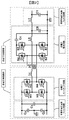
- FIG. 2 is an example of a configuration diagram of a power conversion unit of a DC-DC converter circuit.
- the power conversion unit of the DC-DC converter circuit shown in FIG. 2 includes the high voltage side circuit unit and the low voltage side circuit unit in FIG.
- the DC high voltage power filter circuit is basically composed of a coil and a capacitor.
- the capacitor includes Cx (so-called X capacitor) connected between both terminals of the high-voltage power supply and Cy (so-called Y capacitor) connected between the high-voltage power supply both terminals and the reference potential (GND potential). ) And any of these.
- the filter circuit may be composed of only a capacitor as shown in FIG.
- Cx and Cy do not indicate the number of elements, but are circuit symbol examples. Of course, you may implement
- the high-voltage switching circuit is composed of four MOS-FETs connected in a bridge type (a so-called full-bridge type composed of H1, H2, H3, and H4). Each MOS-FET is provided with a snubber capacitor in parallel.
- the four MOS-FETs (H1, H2, H3, H4) of the high voltage side switching circuit are optimally controlled by the phase shift PWM control by taking in the elements such as the output load amount and the input voltage by the control circuit unit. By performing phase shift PWM control, an alternating high voltage can be generated on the primary side of the transformer.
- the connection of the MOS-FET is an example, and is not limited to the above, and may be realized by another connection method.
- the transformer has an insulating structure on the primary and secondary sides.
- the turn ratio between the primary side and the secondary side of the transformer is set to an optimum turn ratio from the relationship between the input power source and the output power source.
- the transformer input stage is provided with a resonance choke coil Lr for performing a soft switching operation. Using the combined inductance of the resonance choke coil inductance and the transformer leakage inductance, zero voltage switching of the MOS-FET constituting the high voltage side switching circuit is made possible.
- the resonant choke coil is not necessarily required, and a circuit configuration in which these are omitted may be used.
- the low voltage rectifier circuit is composed of four MOS-FETs (S1, S2, S3, S4), a coil L0, and capacitors C0 and Cc.
- the low voltage rectifier circuit performs rectification by a synchronous rectification method and realizes surge absorption by an active clamp method.
- the switching timings of S1, S2, S3, and S4 are coordinated with the phase shift PWM control pulse that takes in the elements such as the output load amount and the input voltage by the control circuit unit and supplies them to the high voltage switching circuit.
- the configuration of the low voltage rectifier circuit unit is not necessarily the same as that of the synchronous rectification method, and may be a diode rectification method, regardless of whether an active clamp method is adopted.
- the DC low-voltage power supply filter circuit includes a coil L1 and a capacitor C1.
- the DC low-voltage power supply filter circuit is not necessarily required, and the acceptance or rejection may be determined according to the product specifications.
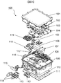
- 3 to 12 are examples of configuration diagrams of the DC-DC converter device 100 according to this embodiment.
- FIG. 3 is a configuration diagram of the DC-DC converter apparatus 100 according to the embodiment of the present invention.
- the DC-DC converter device 100 accommodates the components constituting the above-described DC-DC converter circuit inside a box-shaped casing formed of a conductive metal such as aluminum die cast.
- the upper part of the conductive metal casing 109 is similarly attached with a conductive metal top cover 101 with screws to form a metal box that is electrically connected at the same potential.
- the components constituting the DC-DC converter circuit are accommodated, fixed, held and wired.
- An airtight O-ring 102 is provided between the housing 109 and the upper surface lid 101 so that water or the like does not enter the inside of the housing.
- a cooling channel is formed in the lower part of the casing 109 to cool the components housed in the casing. The cooling channel sandwiches the watertight O-ring 110 and attaches the lower surface lid 111 with screws. By that, it is sealed.
- a pipe 114 is provided on one side of the casing 109.
- the cooling medium is supplied from one of the pipes 114 to the cooling flow path and is recovered from the other.
- the present Example employ
- An input connector 115 is provided on one side of the casing 109.
- the input connector 115 connects wiring for supplying DC high-voltage power from the high-voltage storage battery to a DC-DC converter circuit housed in the housing.
- an output connector 112 is provided for connecting a wiring for outputting a DC low voltage from a DC-DC converter circuit inside the housing.
- a signal connector 113 is provided as a wiring for exchanging vehicle system signals with the DC-DC converter circuit inside the housing.
- the input connector 115, the output connector 112, and the signal connector 113 are attached in a concentrated manner on the same side surface of the housing, but they may be attached to different surfaces.
- the high voltage switching circuit and the DC high voltage power supply filter circuit are mounted on separate substrates.
- the high voltage switching circuit is mounted on the high voltage switching circuit board 118.
- the high voltage switching circuit board 118 is housed on the bottom surface side of the casing 109 in order to efficiently cool the four MOS-FETs that generate a large amount of heat.
- the DC high voltage power filter circuit is mounted on the high voltage power filter substrate 119.
- the high-voltage power supply filter substrate 119 is disposed in the casing 109 so as to be stacked on the upper layer of the high-voltage switching circuit substrate 118.
- the resonance coil 117 corresponding to the resonance choke coil Lr is also a component that generates a large amount of heat, like the MOS-FET, and is therefore disposed on the bottom side of the housing 109.
- the rectifying coil 106 corresponding to the rectifying coil L0 and the filter coil 107 corresponding to the filter coil L1 of the low voltage rectifying circuit are housed in the housing without being mounted on the substrate.
- the rectifying coil 106 and the filter coil 107 are connected by bus bar wiring.
- the capacitor C1 is mounted on an independent capacitor substrate 116.
- the capacitor substrate 116 is disposed closest to the DC low voltage output connector 112 so as to effectively absorb noise. More specifically, the arrangement of the capacitor board 116 and the connection terminal of the DC low-voltage output connector 112 is constituted by the connection with only the output wiring bus bar from the filter coil 107, and other components are arranged. Direct connection without going through.
- S1, S2, S3, S4, C0, Cc are mounted on the low-voltage rectifier circuit board 108.
- the low voltage rectifier circuit board 108 is housed on the bottom side of the housing in order to efficiently cool S1, S2, S3, and S4 that generate large amounts of heat. It should be noted that other methods may be used for the method of configuring the substrate and the method of arranging the components in the low-voltage circuit unit.
- the transformer 105 is disposed between the high voltage side circuit unit and the low voltage side circuit unit, and the primary side winding is connected to the high voltage side circuit and the secondary side winding is connected to the low voltage side circuit. Since the transformer 105 is also a component that generates a large amount of heat, it is disposed on the bottom surface side of the housing 109.
- the high voltage system control circuit unit and the low voltage system control circuit unit are mounted on the same control board 103.
- the high-voltage system control circuit unit and the low-voltage system control circuit unit are clearly separated and mounted for the purpose of avoiding noise interference between them and achieving electrical insulation.
- the high voltage system control circuit unit and the low voltage system control circuit unit constituting the control circuit unit may be configured on separate substrates.
- the frame 104 is housed in the housing 109.
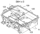
- FIG. 4A is a perspective view of a conductive metal casing 109.
- FIG. 4B is a perspective cross-sectional view of the housing 109 taken along the cross section A of FIG.
- a first wall 120 that protrudes from the bottom surface side of the housing toward the top surface of the housing is formed on the inner surface of the housing 109.
- the space inside the housing 109 is divided into a first space 150 and a second space 151 by the first wall 120.
- components of the high voltage side circuit unit are stored.
- components that generate a large amount of heat that is, the resonance coil 117, the high-voltage switching circuit board 118, and the transformer 105 are housed in the lower layer.
- a high-voltage power supply filter substrate 119 is accommodated in the upper layer.
- components of the low-voltage side circuit unit that is, the low-voltage rectifier circuit board 108, the rectifier coil 106, the filter coil 107, and the capacitor board 116 are accommodated.
- a plurality of screwing columns 123 are installed in the housing 109.
- the screwing column 123 is erected from the housing side toward the top surface of the housing.
- the screwing column 123 is intended to hold and fix the housing 109 and the frame 104 to each other and to make a stable electrical connection.
- the holding and fixing of the frame 104 will be described later with reference to FIG.
- a configuration may be adopted in which the screwing support 123 is formed integrally with a part of the first wall 120.
- FIG. 5 is a top view component layout diagram when the components of the high voltage side circuit unit and the components of the low voltage side circuit unit are stored in the housing 109.
- the left side in the drawing is the first space 150
- the right side in the drawing is the second space 151.
- the resonance coil 117, the high voltage switching circuit board 118, the transformer 105, and the high voltage power supply filter board 119 are accommodated in the first space 150.
- the transformer 105 is disposed close to the first wall 120.
- the transformer 105 has a secondary wiring lead-out portion 105-A connected to the low voltage rectifier circuit board 108. Since the secondary wiring lead-out portion 105-A of the transformer 105 is electrically at a low-voltage side potential on the secondary side, it is preferably arranged in the second space as much as possible. Therefore, the secondary wiring lead-out portion 105-A of the transformer 105 prevents the left side of the first wall 120, that is, the first space 150 from protruding as much as possible. This is because the secondary wiring lead-out portion 105-A is a component that constitutes a part of the transformer 105, and cannot be completely separated into space, and must be partially present in the first space 150. Because.
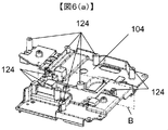
- FIG. 6A is a perspective view of the frame 104.
- the conductive metal frame 104 is disposed above the circuit components constituting the low-voltage side circuit section.
- the frame 104 is formed with a screwing post 124.
- the screw post 124 is provided to mount and fix the control board 103 on which the control circuit unit is mounted.
- the screw post 124 is formed on the upper surface side of the frame 104, that is, on the side where the control board 103 is disposed.
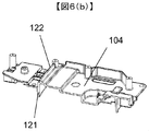
- FIG. 6B is a perspective sectional view of the frame 104 when cut along a section B in FIG.
- the frame 104 has a second wall 121 formed on the lower surface opposite to the upper surface on which the screwing column 124 is formed.
- the second wall 121 protrudes toward the lower surface lid 111 of the housing 109.
- a third wall 122 is formed on the upper surface on which the screwing strut 124 is formed.
- the third wall 122 protrudes toward the upper surface lid 101 of the housing 109.
- FIG. 7 shows a top view component layout in a state where the frame 104 is mounted in the state of FIG.
- the second wall 121 is formed so as to overlap the wall surface position of the first wall 120 when the frame 104 is viewed from above.
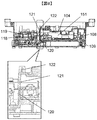
- FIG. 8 is a cross-sectional view taken along the line CC of FIG.
- the second wall 121 formed on the frame 104 protrudes in a direction approaching the tip of the first wall 120 formed on the housing 109.
- the third wall 122 protrudes in a direction opposite to the direction in which the second wall 121 protrudes.
- the frame 104 is screwed and fastened to a screwing support post 123 (see FIG. 4) formed on the housing 109.
- a screwing support post 123 (see FIG. 4) formed on the housing 109.
- the housing 109 and the frame 104 are electrically connected and have the same potential.
- the screw post 123 is formed from the bottom surface side of the housing toward the top surface, but may be formed from the bottom surface of the frame 104 to the bottom surface of the housing.
- the second space 151 in which the low voltage side circuit unit is accommodated is formed by the casing 109, the frame 104, the first wall 120, and the second wall 121. Therefore, since the second space 151 is a space surrounded by a metal conductor that is electrically at the same potential and at the GND potential, a noise shielding effect can be obtained.
- This noise shielding effect prevents high-voltage switching noise generated from the high-voltage side circuit unit and external noise mixed into the high-voltage power supply supplied from the vehicle side from being mixed into the low-voltage side circuit unit. it can. Further, it is possible to suppress noise generated in the low voltage side circuit unit from being mixed into the high voltage side circuit unit and the control circuit.
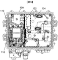
- FIG. 9 shows a top view component layout in a state where the frame 104 is newly mounted.
- the second wall 121 is emphasized to illustrate the arrangement of the second wall 121, but in FIG. 9, the third wall 122 is emphasized to explain the arrangement of the third wall.
- the third wall 122 is formed on the upper surface of the frame 104 toward the upper surface lid portion of the housing 109.
- the wall surface installation position of the third wall 122 is formed close to the second wall 121.
- a plurality of screw struts 124 for holding and fixing the control board 103 and stable electrical connection are also formed in the same direction.
- the wall surface formation position of the third wall 122 is the proximity position of the second wall 121 when viewed from the upper surface of the frame 104, but it does not necessarily have to be close proximity.
- the third wall 122 is formed integrally with the screwing column 124, but may not be formed integrally with the screwing column 124. Further, a larger number of screwing posts 124 may be integrally formed.
- FIG. 10 is a diagram showing a component arrangement of the control board 103.
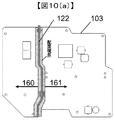
- FIG. 10A is a perspective view showing the component arrangement on the frame 104 side of the control board 103.
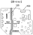
- FIG. 10B is a top view showing the component arrangement on the upper surface side of the control circuit 103.
- a control circuit unit is mounted on the control board 103. As shown in FIG. 1, the control circuit unit is divided into a high voltage system control circuit unit and a low voltage system control circuit unit.
- the frame 104 side control board pattern of the control circuit board 103 includes a first area 160 where the high voltage system control circuit section is mounted and a first area 160 where the low voltage system control circuit section is mounted. It is divided into two areas 161 and mounted. An arrangement boundary is provided between the first region 160 and the second region 161. The arrangement boundary is provided along the third wall 122 as shown in FIG.
- the frame surface side control board pattern at the arrangement boundary along the third wall 122 is provided with a reference potential pattern in the low voltage system control circuit section in the control board 103.
- the control board 103 is composed of a multilayer board, and one of the inner layers is composed of a reference potential in the low voltage system control circuit section, that is, a GND pattern. This GND pattern is laid only in the second region 161 including the arrangement boundary and is as solid as possible.
- the GND pattern is screwed and fixed to a screwing column 124 formed integrally with the third wall 122 provided on the frame 104 and is electrically connected. That is, the reference potential in the low voltage system control circuit unit in the housing 109, the frame 104, and the control board 103 is the same potential.
- the upper control board pattern of the control circuit board 103 includes a third region 162 in which the high voltage system control circuit unit is mounted and a fourth area in which the low voltage system control circuit unit is mounted. It is divided into the area 163 and mounted. An arrangement boundary is provided between the third region 162 and the fourth region 163 as in FIG. The arrangement boundary is provided along the fourth wall 125 (see FIGS. 11 and 12).
- FIG. 11 is a top view showing a state in which the top cover 101 made of conductive metal is mounted.
- the top cover 101 is disposed above the control board 103.
- the top cover 101 is fixed to the housing 109 by screw fastening and is electrically connected to the housing 109. Therefore, the casing 109 and the upper surface lid 101 have the same potential.
- a fourth wall 125 is formed on the upper surface lid 101 on the surface facing the control substrate 103. As shown in FIG. 11, the fourth wall 125 is formed at a position overlapping the third wall 122 when viewed from above. An arrangement boundary between the third region 162 and the fourth region 163 is provided along the fourth wall (see FIG. 10B).
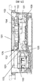
- FIG. 12 is a side sectional view taken along the line CC in FIG. As described above, the first space 150 and the second space 151 are separated by the first wall 120 formed in the housing 109.
- the second space 151 is formed by the housing 109, the frame 104, the first wall 120, and the second wall 121.
- a third space 152 surrounded by the casing 109, the frame 104, the third wall 122, and the control board 103 is formed.
- the third space 152 is separated from the first space 150 by the third wall 122.
- the GND pattern is provided in the inner layer of the control board 103.
- the casing 109, the frame 104, the third wall 122, and the control board inner layer GND pattern are surrounded by a metal conductor having the same electric potential and the GND potential on the upper layer of the second space 151.
- a third space 152 is formed. In the third space 152, only the low voltage system control circuit portion existing in the second region 161 of the control board 103 is arranged.
- the high voltage system control circuit unit existing in the first region 160 of the control board 103 is arranged.
- the frame-side mounting component and the pattern existing in the second region 161 of the control board 103 are included in the third space 152 surrounded by the metal conductor having the same electric potential and the GND electric potential, and the noise shielding effect is obtained. I can get it. Since the noise shielding effect of the third space 152 is effective for the first space 150, the high voltage switching noise generated in the high voltage system control circuit unit and the high voltage side circuit unit, and the high voltage supplied from the vehicle side. It is possible to suppress the external noise mixed in the voltage system power source from being mixed into the low voltage system control circuit unit. Moreover, it is possible to suppress noise generated from the low voltage system control circuit unit from being mixed into the high voltage system control circuit unit or the high voltage side circuit unit.
- the noise shielding effect of the third space 152 is also effective for the second space 151, so that switching noise generated in the low voltage side circuit unit can be prevented from being mixed into the low voltage system control circuit unit. Further, it is possible to suppress noise generated from the low voltage system control circuit unit from being mixed into the low voltage side circuit unit.
- the upper wall 101 is also provided with the fourth wall 125.
- the fourth space 153 surrounded by the metal conductor having the same electric potential and the GND potential is formed on the upper layer of the third space 152 by the casing 109, the upper surface lid 101, the fourth wall 125, and the control board inner layer GND pattern. Is formed.
- the fourth space 153 only the low voltage system control circuit portion existing in the fourth region 163 of the control board 103 is disposed.
- the high voltage system control circuit unit existing in the third region 162 of the control board 103 is arranged.
- the mounting component and the pattern on the upper surface lid 101 side present in the fourth region 163 of the control board 103 are included in the fourth space 153 in a state surrounded by the metal conductor having the same electric potential and the GND potential, and noise shielding is performed. You can get an effect.
- the noise shielding effect of the fourth space 153 can be combined with the noise shielding effect of the third space 152 to obtain a higher noise shielding effect for the first space 150.
- High voltage switching noise generated in the high voltage system control circuit section and the high voltage side circuit section, and external noise mixed in the high voltage system power supply supplied from the vehicle side must be mixed in the low voltage system control circuit section. Can be suppressed.
- the wall-shaped portions of the casing and the frame which are the surfaces constituting the enclosure space, have other purposes as structural parts, such as screw holes and screws for fastening the casing and the frame electrically and mechanically.
- FIG. 13 is an example of circuit arrangement in the casing of the DC-DC converter according to the second embodiment.
- the rectifying coil 106, the filter coil 107, and the capacitor substrate 116 are shielded among the circuit components of the low-voltage circuit unit.
- noise is generated from the rectifying coil 106 to the filter coil 107 and the capacitor substrate 116. Propagate. In such a case, a noise shielding effect can be similarly obtained by providing walls on the casing 109 and the frame 104 as in the first embodiment. As shown in FIG. 13, a fifth wall 126, a sixth wall 127, and a seventh wall 128 are formed around the rectifying coil 106 from the bottom surface of the housing 109 toward the top surface.
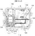
- FIG. 14A is a top view of the state where the frame 104 is mounted in the state shown in FIG.
- walls projecting toward the bottom surface are formed at positions corresponding to the fifth wall 126, the sixth wall 127, and the seventh wall 128.
- An eighth wall 129 is formed at a position corresponding to the fifth wall 126.
- a ninth wall 130 is formed at a position corresponding to the sixth wall 127.
- a tenth wall 131 is formed at a position corresponding to the seventh wall 128.
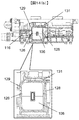
- FIG. 14 (b) is a cross-sectional side view taken along the line EE of FIG. 14 (a).
- the tip of the fifth wall 126 and the eighth wall 129 are formed to face each other.
- the tip of the seventh wall 128 and the tenth wall 131 are formed to face each other.
- the tip of the sixth wall 128 and the ninth wall 130 are also formed to face each other.
- the rectifying coil 106 is surrounded by the fifth wall 126 to the tenth wall 131.
- a space surrounded by a metal conductor having the same electric potential and the GND potential can be formed around the rectifying coil 106, and a noise shielding effect can be obtained. That is, noise that propagates in space from the rectifying coil 106 to the filter coil 107 and the capacitor substrate 116 is suppressed.
- noise is shielded between circuit components that are susceptible to noise from each other, but by applying it to other components as well, the arrangement distance restriction between the components can be relaxed. In addition, since the degree of freedom in component arrangement increases, it is possible to reduce the size.
Landscapes
- Engineering & Computer Science (AREA)
- Power Engineering (AREA)
- Physics & Mathematics (AREA)
- Electromagnetism (AREA)
- Transportation (AREA)
- Mechanical Engineering (AREA)
- Dc-Dc Converters (AREA)
Abstract
Description
(第一の実施例)
図1は、第一の実施例におけるDC-DCコンバータ回路の構成図例である。なお、以下の記述においては高電圧蓄電池から低電圧蓄電池への電力変換を想定して記述を行うが、電力変換方向を制限するものではない。
(第二の実施例)
次に、第一の実施例の応用例として、回路構成部品ごとに空間を形成した第二の実施例について説明する。
101 上面蓋
102 気密Oリング
103 制御基板
104 フレーム
105 トランス
105-A 2次側配線引き出し部
106 整流コイル
107 フィルタコイル
108 低電圧整流回路基板
109 筐体
110 水密Oリング
111 下面蓋
112 出力コネクタ
113 信号コネクタ
114 配管
115 入力コネクタ
116 コンデンサ基板
117 共振コイル
118 高電圧スイッチング回路基板
119 高電圧電源フィルタ基板
120 第1壁
121 第2壁
122 第3壁
123 筐体側ネジ止め支柱
124 フレーム側ネジ止め支柱
125 第4壁
126 第5壁
127 第6壁
128 第7壁
129 第8壁
130 第9壁
131 第10壁
150 第1空間
151 第2空間
152 第3空間
153 第4空間
160 第1領域
161 第2領域
162 第3領域
163 第4領域
Claims (4)
- トランスと電気的に接続される高電圧側回路部と、
前記トランスと電気的に接続される低電圧側回路部と、
前記高電圧側回路部と前記低電圧側回路部を収納する筐体と、
前記低電圧側回路部の駆動を制御する制御回路基板と、
前記制御回路基板を支持するフレームと、を備え、
前記フレームは、前記低電圧側回路部を挟んで、前記筐体の底面と対向する位置に配置され、
前記筐体は、前記高電圧側回路部を収納する第1空間と前記低電圧側回路部を構成する回路部品を収納する第2空間とを隔てる第1壁を有し、
前記フレームは、前記第1壁の先端に近づく方向に突出した第2壁を形成するDC-DCコンバータ。 - 請求項1に記載されたDC-DCコンバータであって、
前記制御回路基板は、前記高電圧側回路部を制御する制御信号を出力する回路部を搭載する第1領域と、前記低電圧側回路部を制御する制御信号を出力する回路部を搭載する第2領域と、を有し、
前記制御回路基板は、前記第1領域が前記高電圧側回路部と対向するようにかつ前記第2領域が前記低電圧側回路部と対向するように、配置されるDC-DCコンバータ。 - 請求項1又は2に記載されたいずれかのDC-DCコンバータであって、
前記フレームは、前記第2壁が突出する方向とは反対の方向に突出する第3壁を形成し、
前記第3壁は、前記フレームと前記制御回路基板との間の第3空間と前記第1空間を隔てる位置に配置されるDC-DCコンバータ。 - 請求項3に記載されたDC-DCコンバータであって、
前記高電圧側回路部は、高電圧側スイッチング回路部と、フィルタ機能を有するコンデンサと、により構成され、
前記高電圧側スイッチング回路部は、前記筐体の底面に配置され、
前記コンデンサは、前記高電圧側スイッチング回路部よりも、前記筐体の底面から離れた位置に配置されるDC-DCコンバータ。
Priority Applications (2)
| Application Number | Priority Date | Filing Date | Title |
|---|---|---|---|
| DE112013006238.0T DE112013006238B4 (de) | 2012-12-28 | 2013-11-06 | Gleichstrom/Gleichstrom-Wandler |
| US14/653,420 US9776514B2 (en) | 2012-12-28 | 2013-11-06 | DC-DC converter |
Applications Claiming Priority (2)
| Application Number | Priority Date | Filing Date | Title |
|---|---|---|---|
| JP2012286604A JP6101484B2 (ja) | 2012-12-28 | 2012-12-28 | Dc−dcコンバータ |
| JP2012-286604 | 2012-12-28 |
Publications (1)
| Publication Number | Publication Date |
|---|---|
| WO2014103518A1 true WO2014103518A1 (ja) | 2014-07-03 |
Family
ID=51020617
Family Applications (1)
| Application Number | Title | Priority Date | Filing Date |
|---|---|---|---|
| PCT/JP2013/079952 Ceased WO2014103518A1 (ja) | 2012-12-28 | 2013-11-06 | Dc-dcコンバータ |
Country Status (4)
| Country | Link |
|---|---|
| US (1) | US9776514B2 (ja) |
| JP (1) | JP6101484B2 (ja) |
| DE (1) | DE112013006238B4 (ja) |
| WO (1) | WO2014103518A1 (ja) |
Cited By (1)
| Publication number | Priority date | Publication date | Assignee | Title |
|---|---|---|---|---|
| CN107487208A (zh) * | 2016-06-13 | 2017-12-19 | 丰田自动车株式会社 | 电力变换器的车载构造 |
Families Citing this family (16)
| Publication number | Priority date | Publication date | Assignee | Title |
|---|---|---|---|---|
| JP6045340B2 (ja) * | 2012-12-28 | 2016-12-14 | 日立オートモティブシステムズ株式会社 | Dc−dcコンバータ装置 |
| SG2013069224A (en) * | 2013-09-13 | 2015-04-29 | Rockwell Automation Asia Pacific Business Ctr Pte Ltd | Motor drive with inherent power isolation |
| WO2015053139A1 (ja) * | 2013-10-07 | 2015-04-16 | 日立オートモティブシステムズ株式会社 | 電力変換装置 |
| JP6408857B2 (ja) * | 2014-10-20 | 2018-10-17 | ローム株式会社 | ゲートドライバユニットおよびパワーモジュール |
| US10086703B2 (en) | 2014-12-31 | 2018-10-02 | General Electric Company | System and method for controlling electrically driven accessories |
| JP6487834B2 (ja) * | 2015-12-15 | 2019-03-20 | 日立オートモティブシステムズ株式会社 | 電力変換装置 |
| US10160332B2 (en) * | 2016-07-27 | 2018-12-25 | GM Global Technology Operations LLC | Electric power distribution system and topology |
| JP6670353B2 (ja) * | 2018-09-21 | 2020-03-18 | ローム株式会社 | ゲートドライバユニットおよびパワーモジュール |
| JP7127518B2 (ja) * | 2018-12-12 | 2022-08-30 | 株式会社デンソー | 電源装置 |
| JP7069075B2 (ja) * | 2019-03-26 | 2022-05-17 | 本田技研工業株式会社 | 電源システム |
| JP7098025B1 (ja) * | 2021-06-09 | 2022-07-08 | 三菱電機株式会社 | 電力変換装置 |
| DE102021115272A1 (de) | 2021-06-14 | 2022-12-15 | Schaeffler Technologies AG & Co. KG | Elektrische Schaltungsanordnung und elektrische Antriebsanordnung |
| US11804782B2 (en) * | 2022-01-28 | 2023-10-31 | Analog Devices, Inc. | Active-clamp current-fed push-pull converter for bidirectional power transfer |
| CA3253474A1 (en) * | 2022-03-18 | 2023-09-21 | Horton, Inc. | HIGH VOLTAGE ELECTRIC FAN SYSTEM |
| DE102023207993A1 (de) * | 2023-08-22 | 2025-02-27 | Zf Friedrichshafen Ag | Spannungswandler für ein Fahrzeug |
| JP2025118169A (ja) | 2024-01-31 | 2025-08-13 | 株式会社アイシン | 電力変換装置 |
Citations (5)
| Publication number | Priority date | Publication date | Assignee | Title |
|---|---|---|---|---|
| JPH11299260A (ja) * | 1998-04-15 | 1999-10-29 | Matsushita Electric Works Ltd | 電源装置 |
| JP2002214729A (ja) * | 2001-01-19 | 2002-07-31 | Canon Inc | 放射線画像撮影装置 |
| JP2007180683A (ja) * | 2005-12-27 | 2007-07-12 | Kyocera Corp | 携帯無線機 |
| JP2010245232A (ja) * | 2009-04-03 | 2010-10-28 | Denso Corp | 高周波シールドケース |
| JP2013090533A (ja) * | 2011-10-21 | 2013-05-13 | Denso Corp | 電源装置 |
Family Cites Families (7)
| Publication number | Priority date | Publication date | Assignee | Title |
|---|---|---|---|---|
| US7834575B2 (en) * | 2008-04-01 | 2010-11-16 | International Rectifier Corporation | Gate-driver IC with HV-isolation, especially hybrid electric vehicle motor drive concept |
| JP5606027B2 (ja) * | 2009-09-07 | 2014-10-15 | ダイヤモンド電機株式会社 | ブロック型電力モジュール及び電力変換装置 |
| JP2012178937A (ja) | 2011-02-28 | 2012-09-13 | Hitachi Automotive Systems Ltd | 電力変換装置 |
| JP5743851B2 (ja) * | 2011-10-31 | 2015-07-01 | 日立オートモティブシステムズ株式会社 | 電子装置 |
| WO2013077311A1 (ja) * | 2011-11-21 | 2013-05-30 | 株式会社オートネットワーク技術研究所 | Dc-dcコンバータ |
| JP6012330B2 (ja) * | 2012-08-03 | 2016-10-25 | 日立オートモティブシステムズ株式会社 | Dcdcコンバータ |
| JPWO2014033852A1 (ja) * | 2012-08-29 | 2016-08-08 | 三菱電機株式会社 | 車載用電力変換装置 |
-
2012
- 2012-12-28 JP JP2012286604A patent/JP6101484B2/ja active Active
-
2013
- 2013-11-06 DE DE112013006238.0T patent/DE112013006238B4/de active Active
- 2013-11-06 WO PCT/JP2013/079952 patent/WO2014103518A1/ja not_active Ceased
- 2013-11-06 US US14/653,420 patent/US9776514B2/en active Active
Patent Citations (5)
| Publication number | Priority date | Publication date | Assignee | Title |
|---|---|---|---|---|
| JPH11299260A (ja) * | 1998-04-15 | 1999-10-29 | Matsushita Electric Works Ltd | 電源装置 |
| JP2002214729A (ja) * | 2001-01-19 | 2002-07-31 | Canon Inc | 放射線画像撮影装置 |
| JP2007180683A (ja) * | 2005-12-27 | 2007-07-12 | Kyocera Corp | 携帯無線機 |
| JP2010245232A (ja) * | 2009-04-03 | 2010-10-28 | Denso Corp | 高周波シールドケース |
| JP2013090533A (ja) * | 2011-10-21 | 2013-05-13 | Denso Corp | 電源装置 |
Cited By (2)
| Publication number | Priority date | Publication date | Assignee | Title |
|---|---|---|---|---|
| CN107487208A (zh) * | 2016-06-13 | 2017-12-19 | 丰田自动车株式会社 | 电力变换器的车载构造 |
| CN107487208B (zh) * | 2016-06-13 | 2019-12-17 | 丰田自动车株式会社 | 电力变换器的车载构造 |
Also Published As
| Publication number | Publication date |
|---|---|
| JP6101484B2 (ja) | 2017-03-22 |
| JP2014131371A (ja) | 2014-07-10 |
| DE112013006238T5 (de) | 2015-10-08 |
| US20150306960A1 (en) | 2015-10-29 |
| US9776514B2 (en) | 2017-10-03 |
| DE112013006238B4 (de) | 2026-08-20 |
Similar Documents
| Publication | Publication Date | Title |
|---|---|---|
| JP6101484B2 (ja) | Dc−dcコンバータ | |
| JP5743851B2 (ja) | 電子装置 | |
| US10128770B2 (en) | Converter and electric power conversion apparatus | |
| US9866127B2 (en) | Electrical power converting device | |
| CN107925356B (zh) | Dcdc转换器一体型充电器 | |
| US9425695B2 (en) | DC-DC converter | |
| US9814154B2 (en) | Power converter | |
| JP4936466B2 (ja) | パワー半導体ユニット | |
| WO2016136115A1 (ja) | 電力変換装置 | |
| US9935558B2 (en) | DC-DC converter apparatus including single drive circuit board arranged at predetermined interval from metal base | |
| JP2020061892A (ja) | 電圧変換装置 | |
| JP7247748B2 (ja) | 電力変換装置 | |
| JP2020061893A (ja) | 電力変換装置 | |
| JP2019088137A (ja) | 電力変換装置 | |
| JP6060664B2 (ja) | 電源装置 | |
| WO2025182101A1 (ja) | 電力変換装置 | |
| JP2017135819A (ja) | 電力変換装置 | |
| JP6119517B2 (ja) | 電力変換装置 | |
| JP2016019458A (ja) | 電力変換装置 |
Legal Events
| Date | Code | Title | Description |
|---|---|---|---|
| 121 | Ep: the epo has been informed by wipo that ep was designated in this application |
Ref document number: 13867116 Country of ref document: EP Kind code of ref document: A1 |
|
| WWE | Wipo information: entry into national phase |
Ref document number: 14653420 Country of ref document: US |
|
| WWE | Wipo information: entry into national phase |
Ref document number: 112013006238 Country of ref document: DE Ref document number: 1120130062380 Country of ref document: DE |
|
| 122 | Ep: pct application non-entry in european phase |
Ref document number: 13867116 Country of ref document: EP Kind code of ref document: A1 |