WO2014103409A1 - 電子・電気機器用銅合金、電子・電気機器用銅合金薄板、電子・電気機器用導電部品及び端子 - Google Patents
電子・電気機器用銅合金、電子・電気機器用銅合金薄板、電子・電気機器用導電部品及び端子 Download PDFInfo
- Publication number
- WO2014103409A1 WO2014103409A1 PCT/JP2013/067863 JP2013067863W WO2014103409A1 WO 2014103409 A1 WO2014103409 A1 WO 2014103409A1 JP 2013067863 W JP2013067863 W JP 2013067863W WO 2014103409 A1 WO2014103409 A1 WO 2014103409A1
- Authority
- WO
- WIPO (PCT)
- Prior art keywords
- mass
- copper alloy
- electronic
- less
- ratio
- Prior art date
Links
Images

Classifications
-
- C—CHEMISTRY; METALLURGY
- C22—METALLURGY; FERROUS OR NON-FERROUS ALLOYS; TREATMENT OF ALLOYS OR NON-FERROUS METALS
- C22C—ALLOYS
- C22C9/00—Alloys based on copper
- C22C9/04—Alloys based on copper with zinc as the next major constituent
-
- C—CHEMISTRY; METALLURGY
- C22—METALLURGY; FERROUS OR NON-FERROUS ALLOYS; TREATMENT OF ALLOYS OR NON-FERROUS METALS
- C22F—CHANGING THE PHYSICAL STRUCTURE OF NON-FERROUS METALS AND NON-FERROUS ALLOYS
- C22F1/00—Changing the physical structure of non-ferrous metals or alloys by heat treatment or by hot or cold working
- C22F1/002—Changing the physical structure of non-ferrous metals or alloys by heat treatment or by hot or cold working by rapid cooling or quenching; cooling agents used therefor
-
- C—CHEMISTRY; METALLURGY
- C22—METALLURGY; FERROUS OR NON-FERROUS ALLOYS; TREATMENT OF ALLOYS OR NON-FERROUS METALS
- C22F—CHANGING THE PHYSICAL STRUCTURE OF NON-FERROUS METALS AND NON-FERROUS ALLOYS
- C22F1/00—Changing the physical structure of non-ferrous metals or alloys by heat treatment or by hot or cold working
- C22F1/02—Changing the physical structure of non-ferrous metals or alloys by heat treatment or by hot or cold working in inert or controlled atmosphere or vacuum
-
- C—CHEMISTRY; METALLURGY
- C22—METALLURGY; FERROUS OR NON-FERROUS ALLOYS; TREATMENT OF ALLOYS OR NON-FERROUS METALS
- C22F—CHANGING THE PHYSICAL STRUCTURE OF NON-FERROUS METALS AND NON-FERROUS ALLOYS
- C22F1/00—Changing the physical structure of non-ferrous metals or alloys by heat treatment or by hot or cold working
- C22F1/08—Changing the physical structure of non-ferrous metals or alloys by heat treatment or by hot or cold working of copper or alloys based thereon
-
- H—ELECTRICITY
- H01—ELECTRIC ELEMENTS
- H01B—CABLES; CONDUCTORS; INSULATORS; SELECTION OF MATERIALS FOR THEIR CONDUCTIVE, INSULATING OR DIELECTRIC PROPERTIES
- H01B1/00—Conductors or conductive bodies characterised by the conductive materials; Selection of materials as conductors
- H01B1/02—Conductors or conductive bodies characterised by the conductive materials; Selection of materials as conductors mainly consisting of metals or alloys
- H01B1/026—Alloys based on copper
Definitions
- the present invention relates to a Cu—Zn—Sn based copper for electronic / electric equipment used as a conductive part for electronic / electric equipment such as a connector of a semiconductor device, other terminals, or a movable conductive piece of an electromagnetic relay, or a lead frame.
- the present invention relates to an alloy, a copper alloy thin plate for electronic / electric equipment, a conductive component for electronic / electric equipment, and a terminal using the alloy.
- Cu-Zn alloy from the viewpoint of balance of strength, workability, cost, etc. as a material for semiconductor device connectors, other terminals, or movable conductive pieces of electromagnetic relays, and conductive parts for electronic and electrical equipment such as lead frames Has been widely used.
- the surface of the base material (base plate) made of Cu—Zn alloy should be used with tin (Sn) plating.
- Sn is further added to the Cu-Zn alloy in order to improve the recyclability of Sn plating material and improve the strength.
- Cu—Zn—Sn alloy is used.
- conductive parts for electronic and electrical equipment such as connectors are generally formed into a predetermined shape by punching a thin plate (rolled plate) having a thickness of about 0.05 to 1.0 mm, and at least a part thereof is bent. It is manufactured by applying. In this case, the conductive component is brought into contact with the mating conductive member in the vicinity of the bent portion to obtain an electrical connection with the mating conductive member, and the contact state with the mating conductive material is maintained by the spring property of the bent portion.
- rolled plate a thin plate having a thickness of about 0.05 to 1.0 mm
- the copper alloy for electronic / electric equipment used for such electronic / electric equipment conductive parts is excellent in conductivity, rollability and punchability. Furthermore, as described above, in the case of a copper alloy that constitutes a connector or the like that is used to maintain a contact state with a counterpart conductive member in the vicinity of the bent portion due to the bending property of the bent portion, as described above Further, it is required to have excellent bending workability and stress relaxation resistance.
- Patent Documents 1 to 3 propose methods for improving the stress relaxation resistance of Cu—Zn—Sn alloys.
- Patent Document 1 states that the stress relaxation resistance can be improved by adding Ni to a Cu—Zn—Sn alloy to produce a Ni—P compound, and the addition of Fe can also reduce stress relaxation. It has been shown to be effective in improving the characteristics.
- Patent Document 2 describes that strength, elasticity, and heat resistance can be improved by adding Ni and Fe together with P to a Cu—Zn—Sn alloy to form a compound. The above-mentioned improvement in strength, elasticity and heat resistance means improvement in stress relaxation resistance of the copper alloy.
- Patent Document 3 describes that stress relaxation resistance can be improved by adding Ni to a Cu—Zn—Sn alloy and adjusting the Ni / Sn ratio within a specific range. Further, it is described that the addition of a small amount of Fe is effective in improving the stress relaxation resistance. Furthermore, in Patent Document 4 for lead frame materials, Ni and Fe are added together with P to a Cu—Zn—Sn alloy, and the atomic ratio of (Fe + Ni) / P is within a range of 0.2-3. It is described that the stress relaxation resistance can be improved by adjusting to the above and generating Fe-P compounds, Ni-P compounds, and Fe-Ni-P compounds.
- Japanese Patent Laid-Open No. 05-33087 JP 2006-283060 A Japanese Patent No. 3953357 Japanese Patent No. 3717321
- Patent Documents 1 and 2 only the individual contents of Ni, Fe, and P are considered, and the adjustment of such individual contents does not necessarily ensure the stress relaxation resistance.
- Patent Document 3 discloses that the Ni / Sn ratio is adjusted, but the relationship between the P compound and the stress relaxation resistance is not considered at all, and sufficient and reliable stress relaxation resistance is obtained. It was not possible to improve.
- Patent Document 4 only the total amount of Fe, Ni, and P and the atomic ratio of (Fe + Ni) / P were adjusted, and the stress relaxation resistance could not be sufficiently improved.
- the conventionally proposed methods cannot sufficiently improve the stress relaxation resistance of the Cu—Zn—Sn alloy. For this reason, in the connector having the above-described structure, the residual stress is relaxed over time or in a high-temperature environment, and the contact pressure with the counterpart conductive member is not maintained, and inconveniences such as poor contact are likely to occur at an early stage. There was a problem. In order to avoid such a problem, conventionally, the thickness of the material has to be increased, leading to an increase in material cost and weight. Therefore, further reliable and sufficient improvement of the stress relaxation resistance is strongly desired.
- the present invention has been made in the background as described above, and has excellent stress relaxation resistance, proof stress-bending balance, and can reduce the thickness of component materials compared to conventional copper for electronic and electrical equipment. It is an object to provide an alloy, a copper alloy thin plate for electronic / electric equipment, a component for electronic / electric equipment, and a terminal using the alloy.
- the inventors of the present invention added a proper amount of Ni and Fe to a Cu—Zn—Sn alloy and added a proper amount of P, and the Fe / Ni content ratio Fe / Ni.
- the ratio of the total content of Ni and Fe (Ni + Fe) to the content of P (Ni + Fe) / P and the ratio of the content of Sn to the total content of Ni and Fe (Ni + Fe) Sn / (Ni + Fe) are adjusted within the appropriate ranges in terms of atomic ratios, so that precipitates containing Fe and / or Ni and P are appropriately deposited, and at the same time, ⁇ 220 ⁇ face on the surface of the plate material or strip material, etc.
- the copper alloy for electronic / electrical equipment according to the first aspect of the present invention has Zn in excess of 2 mass% and less than 23 mass%, Sn in the range of 0.1 mass% to 0.9 mass%, and Ni in the range of 0.05 mass% to 1. Less than 0 mass%, Fe is 0.001 mass% or more and less than 0.10 mass%, P is contained in 0.005 mass% or more and 0.1 mass% or less, and the balance is made of Cu and inevitable impurities, Fe content and Ni content
- the ratio Fe / Ni in terms of the atomic ratio satisfies 0.002 ⁇ Fe / Ni ⁇ 1.5, and the ratio of the total content of Ni and Fe (Ni + Fe) to the content of P (Ni + Fe) / P
- the atomic ratio satisfies 3 ⁇ (Ni + Fe) / P ⁇ 15
- the ratio Sn / (Ni + Fe) between the Sn content and the total amount of Ni and Fe (Ni + Fe) is 0.3 ⁇ S
- Ni and Fe are added together with P, and the addition ratio among Sn, Ni, Fe, and P is regulated, whereby the parent phase ( ⁇ phase [Ni, Fe] -P-based precipitates containing Fe and / or Ni and P precipitated from the main body) are appropriately present, and at the same time, the ⁇ 220 ⁇ plane X-ray diffraction intensity ratio R ⁇ 220 on one surface ⁇ Is suppressed to 0.8 or less, it is sufficiently excellent in stress relaxation resistance, high in strength (proof stress), and excellent in bending workability.
- the [Ni, Fe] -P-based precipitates are Ni—Fe—P ternary precipitates, or Fe—P or Ni—P binary precipitates.
- a multi-component precipitate containing, for example, Cu, Zn, Sn as main components, O, S, C, Co, Cr, Mo, Mn, Mg, Zr, Ti, or the like as impurities is included.
- the [Ni, Fe] -P-based precipitates exist in the form of phosphides or alloys in which phosphorus is dissolved.
- the copper alloy for electronic / electrical equipment according to the second aspect of the present invention has Zn in excess of 2 mass% and less than 23 mass%, Sn in the range of 0.1 mass% to 0.9 mass%, and Ni in the range of 0.05 mass% to 1.0 mass%.
- the ratio of the total content of Fe and Co to the content of Ni (Fe + Co) / Ni is made of impurities and satisfies an atomic ratio of 0.002 ⁇ (Fe + Co) / Ni ⁇ 1.5, and Ni, Fe and The ratio (Ni + Fe + Co) / P of the total Co content (Ni + Fe + Co) to the P content satisfies 3 ⁇ (Ni + Fe + Co) / P ⁇ 15 in atomic ratio.
- the X-ray diffraction intensity is the X-ray diffraction intensity from the ⁇ phase of the copper alloy matrix.
- the copper alloy according to the second aspect is the copper alloy according to the first aspect, further including Co in an amount of 0.001 mass% to less than 0.1 mass%, and a total content of Fe and Co;
- Ratio of Ni content (Fe + Co) / Ni is an atomic ratio satisfying (Fe + Co) / Ni ⁇ 1.5, and the ratio of the total content of Ni, Fe and Co (Ni + Fe + Co) to the content of P (Ni + Fe + Co) / P satisfies the atomic ratio (Ni + Fe + Co) / P ⁇ 15, and the ratio Sn / (Ni + Fe + Co) between the Sn content and the total content of Ni, Fe and Co (Ni + Fe + Co) is the atomic ratio. Therefore, it may satisfy 0.3 ⁇ Sn / (Ni + Fe + Co).
- the copper alloy for electronic and electrical equipment having the above-described configuration, by adding Ni, Fe and Co together with P, and appropriately regulating the addition ratio among Sn, Ni, Fe, Co and P, [Ni, Fe, Co] -P-based precipitates containing Fe and at least one element selected from Ni, Co, and P precipitated from the matrix (mainly ⁇ -phase) are appropriately present, Since the X-ray diffraction intensity ratio R ⁇ 220 ⁇ of the ⁇ 220 ⁇ surface on the surface is suppressed to 0.8 or less, it is sufficiently excellent in stress relaxation resistance, and also has high strength (proof stress) and bending workability. It will be excellent.
- the [Ni, Fe, Co] -P-based precipitate is a quaternary precipitate of Ni-Fe-Co-P, or Ni-Fe-P, Ni-Co-P, or Fe-Co.
- the [Ni, Fe, Co] -P-based precipitates exist in the form of phosphides or alloys in which phosphorus is dissolved.
- the copper alloy according to the first or second aspect may be a rolled material, and one surface (rolled surface) may satisfy the condition of the X-ray diffraction intensity on the one surface.
- the rolled material may have a form of a plate material or a strip material, and the plate surface or the surface of the strip may satisfy the X-ray diffraction intensity condition on the one surface.
- the copper alloy for electronic / electric equipment according to the first or second aspect preferably has a mechanical property of 0.2% proof stress of 300 MPa or more.
- Such a copper alloy for electronic and electrical equipment having a mechanical property of 0.2% proof stress of 300 MPa or more is suitable for conductive parts that require particularly high strength, such as a movable conductive piece of an electromagnetic relay or a spring part of a terminal. Is suitable.
- the copper alloy thin plate for electronic / electrical equipment according to the third aspect of the present invention has a thin plate body made of a rolled material of the copper alloy for electronic / electrical equipment according to the first or second aspect described above, and the thin plate
- the copper alloy thin plate is characterized in that the thickness of the main body is in the range of 0.05 mm to 1.0 mm.
- the copper alloy thin plate main body may be a thin plate (tape-like copper alloy) having a strip shape.
- the copper alloy thin plate for electronic / electric equipment having such a configuration can be suitably used for connectors, other terminals, movable conductive pieces of electromagnetic relays, lead frames, and the like.
- the above-mentioned copper alloy thin plate for electronic / electric equipment has an X-ray diffraction intensity from the ⁇ 111 ⁇ plane of the parent phase ( ⁇ phase), an X-ray diffraction intensity from the ⁇ 200 ⁇ plane, ⁇ 220 ⁇ on the surface of the thin plate body.
- Sn plating may be given to the surface of the said thin-plate main body. That is, the said copper alloy thin plate may have a thin plate main body (base material) and the Sn plating layer formed on the surface of the said thin plate main body. Sn plating may be given to the single side
- the base material of the Sn plating is made of a Cu—Zn—Sn alloy containing 0.1 mass% or more and 0.9 mass% or less of Sn. It can be recovered as Cu—Zn alloy scrap to ensure good recyclability.
- a conductive component for electronic / electrical equipment comprising the above-described copper alloy for electronic / electrical equipment.
- a conductive component for electronic / electrical equipment comprising the above-described copper alloy thin plate for electronic / electrical equipment.
- the conductive parts for electronic / electrical equipment in the present invention include terminals, connectors, relays, lead frames and the like.
- a terminal according to a sixth aspect of the present invention is characterized by comprising the above-described copper alloy for electronic and electrical equipment. Furthermore, a terminal according to a seventh aspect of the present invention is characterized by comprising the above-described copper alloy thin plate for electronic and electrical equipment.
- the terminals in the present invention include connectors and the like.
- the stress relaxation resistance is excellent, so that residual stress is less likely to be relaxed over time or in a high temperature environment.
- the structure is configured to press contact with the mating conductive material, the contact pressure with the mating conductive member can be maintained.
- ADVANTAGE OF THE INVENTION According to this invention, it is excellent in a stress relaxation characteristic, a proof stress-bending balance, and can reduce the thickness of a component material compared with the past,
- the copper alloy for electronic / electric equipment using the same, The copper alloy for electronic / electric equipment using the same Thin plates, parts for electronic / electrical equipment, and terminals can be provided.
- the copper alloy for electronic and electric apparatuses which is one Embodiment of this invention is demonstrated.
- the copper alloy for electronic / electrical devices according to the present embodiment is more than 2 mass% of Zn and less than 23 mass%, Sn is 0.1 mass% to 0.9 mass%, Ni is 0.05 mass% to less than 1.0 mass%, Fe is contained in an amount of 0.001 mass% to less than 0.10 mass%, P is contained in an amount of 0.005 mass% to 0.1 mass%, and the balance is composed of Cu and inevitable impurities.
- ratio Fe / Ni of content of Fe and content of Ni is atomic ratio, following (1)
- Formula 0.002 ⁇ Fe / Ni ⁇ 1 .5
- the ratio of the total content of Ni and Fe (Ni + Fe) to the content of P (Ni + Fe) / P is an atomic ratio expressed by the following formula (2) 3 ⁇ (Ni + Fe) / P ⁇ 15
- the ratio Sn / (Ni + Fe) between the Sn content, the Ni content and the total Fe content (Ni + Fe) is an atomic ratio, and the following equation (3): 0.3 ⁇ Sn / (Ni + Fe) ⁇ 5 (3) It is determined to satisfy.
- the copper alloy for electronic / electrical equipment which is this embodiment may contain 0.001 mass% or more and less than 0.10 mass% of Co other than said Zn, Sn, Ni, Fe, and P.
- the Fe content is set within a range of 0.001 mass% or more and less than 0.10 mass%.
- the ratio of the total content of Fe and Co to the content of Ni (Fe + Co) / Ni is the atomic ratio as the content ratio between the alloy elements.
- the ratio (Ni + Fe + Co) / P of the total content of Ni, Fe and Co (Ni + Fe + Co) to the content of P is an atomic ratio, and the following (2 ′) formula 3 ⁇ (Ni + Fe + Co) / P ⁇ 15 ... (2 ') Further, the ratio Sn / (Ni + Fe + Co) of the Sn content and the total content of Ni, Fe and Co (Ni + Fe + Co) is expressed by the following formula (3 ′): 0.3 ⁇ Sn / (Ni + Fe + Co) ) ⁇ 5 ... (3 ') It is determined to satisfy.
- Ratio of Ni content (Fe + Co) / Ni is an atomic ratio satisfying (Fe + Co) / Ni ⁇ 1.5, and the ratio of the total content of Ni, Fe and Co (Ni + Fe + Co) to the content of P (Ni + Fe + Co) / P satisfies the atomic ratio (Ni + Fe + Co) / P ⁇ 15, and the ratio Sn / (Ni + Fe + Co) between the Sn content and the total content of Ni, Fe and Co (Ni + Fe + Co) is the atomic ratio.
- the above-described expressions (1 ′), (2 ′), and (3 ′) are also satisfied.
- Zinc (Zn) more than 2 mass% and less than 23 mass%
- Zn is a basic alloy element in the copper alloy which is the subject of this embodiment, and is an element effective in improving strength and springiness. Moreover, since Zn is cheaper than Cu, it is effective in reducing the material cost of the copper alloy. If Zn is 2 mass% or less, the effect of reducing the material cost cannot be sufficiently obtained. On the other hand, when Zn is 23 mass% or more, the corrosion resistance is lowered and the cold rolling property of the copper alloy is also lowered. Therefore, in the present embodiment, the Zn content is in the range of more than 2 mass% and less than 23 mass%. The Zn content is preferably in the range of more than 2 mass% and not more than 15 mass%, and more preferably in the range of not less than 3 mass% and not more than 15 mass%.
- Addition of Sn is effective in improving the strength of the copper alloy, and is advantageous in improving the recyclability of the Cu-Zn alloy material with Sn plating. Furthermore, it has been found by the present inventors that Sn, if Ni coexists with Ni and Fe, contributes to the improvement of the stress relaxation resistance of the copper alloy. If Sn is less than 0.1 mass%, these effects cannot be sufficiently obtained. On the other hand, if Sn exceeds 0.9 mass%, the hot workability and the cold rollability are deteriorated. There is a possibility that cracking may occur in cold rolling, and the electrical conductivity also decreases. Therefore, in the present embodiment, the Sn content is in the range of 0.1 mass% to 0.9 mass%. The Sn content is particularly preferably in the range of 0.2 mass% to 0.8 mass% even within the above range.
- the presence of these precipitates can greatly improve the stress relaxation resistance of the copper alloy.
- the stress relaxation resistance of the copper alloy can be improved even by solid solution strengthening.
- the addition amount of Ni is less than 0.05 mass%, the stress relaxation resistance cannot be sufficiently improved.
- the addition amount of Ni becomes 1.0 mass% or more, the solid solution Ni increases and the conductivity decreases, and the cost increases due to an increase in the amount of expensive Ni raw materials used. Therefore, in the present embodiment, the Ni content is in the range of 0.05 mass% or more and less than 1.0 mass%. In addition, it is preferable to make content of Ni into the range of 0.2 mass% or more and less than 0.8 mass% especially also in said range.
- the presence of these precipitates can greatly improve the stress relaxation resistance of the copper alloy.
- the addition amount of Fe is less than 0.001 mass%, the effect of pinning the crystal grain boundary cannot be sufficiently obtained, and sufficient strength cannot be obtained.
- the amount of Fe added is 0.10 mass% or more, no further improvement in strength is observed, the amount of solid solution Fe increases, the conductivity of the copper alloy decreases, and the cold rolling property also decreases. End up. Therefore, in the present embodiment, the Fe content is set within a range of 0.001 mass% or more and less than 0.10 mass%. In addition, it is preferable to make content of Fe into the range of 0.002 mass% or more and 0.08 mass% or less especially also in said range.
- Co Co
- Co is not necessarily an essential additive element, but if a small amount of Co is added together with Ni, Fe, and P, [Ni, Fe, Co] -P A system precipitate is generated, and the stress relaxation resistance of the copper alloy can be further improved.
- the amount of Co addition is less than 0.001 mass%, the effect of further improving the stress relaxation resistance by Co addition cannot be obtained.
- the amount of Co added is 0.10 mass% or more, the amount of solid solution Co increases, the conductivity of the copper alloy decreases, and the cost increases due to an increase in the amount of expensive Co raw material used.
- the Co content when Co is added, is set within a range of 0.001 mass% or more and less than 0.10 mass%. Even within the above range, the Co content is preferably within the range of 0.002 mass% to 0.08 mass%. Even when Co is not actively added, Co of less than 0.001 mass% may be contained as an impurity.
- Phosphorus (P): 0.005 mass% or more and 0.10 mass% or less P has high bonding properties with Fe, Ni, and Co, and if Ni and Fe are contained together with Fe and Ni, [Ni, Fe] -P-based precipitates can be deposited, and if an appropriate amount of P is contained together with Fe, Ni, Co, [Ni, Fe, Co] -P-based precipitates can be deposited, and these The presence of the precipitate can improve the stress relaxation resistance of the copper alloy.
- the content of P is set in the range of 0.005 mass% or more and 0.10 mass% or less.
- the content of P is particularly preferably in the range of 0.01 mass% to 0.08 mass% even within the above range.
- P is an element that is inevitably mixed in from the melting material of the copper alloy. Therefore, in order to regulate the amount of P as described above, it is desirable to appropriately select the melting material.
- the balance of the above elements may basically be Cu and inevitable impurities.
- unavoidable impurities Mg, Al, Mn, Si, (Co), Cr, Ag, Ca, Sr, Ba, Sc, Y, Hf, V, Nb, Ta, Mo, W, Re, Ru , Os, Se, Te, Rh, Ir, Pd, Pt, Au, Cd, Ga, In, Li, Ge, As, Sb, Ti, Tl, Pb, Bi, Be, N, Hg, B, Zr, rare earth Etc.
- These inevitable impurities are desirably 0.3% by mass or less in total.
- the (Ni + Fe + Co) / P ratio is 15 or more, the electrical conductivity of the copper alloy decreases due to the increase in the proportion of Ni, Fe, and Co dissolved, and the amount of expensive Co and Ni raw materials used is relatively high. Increasing costs will increase costs. Therefore, the (Ni + Fe + Co) / P ratio is regulated within the above range. Note that the (Ni + Fe + Co) / P ratio is preferably in the range of more than 3 and 12 or less even in the above range.
- each alloy element is adjusted not only to the individual content but also to the ratio between each element so that the formulas (1) to (3) or (1 ′) to (3 ′) are satisfied.
- [Ni, Fe] -P-based precipitates or [Ni, Fe, Co] -P-based precipitates are dispersed and precipitated from the parent phase (mainly ⁇ -phase). It is considered that the stress relaxation resistance is improved by the dispersion and precipitation of the precipitates.
- the component composition is adjusted as described above, but also one plate surface (plate surface of plate material or surface of strip material) as follows: Defines the X diffraction intensity ratio of the parent phase ( ⁇ phase).
- the X-ray diffraction intensity from the ⁇ 111 ⁇ plane on one plate surface is expressed as I ⁇ 111 ⁇
- the X-ray diffraction intensity from the ⁇ 200 ⁇ plane is represented by I ⁇ 200 ⁇
- the X-ray diffraction intensity from the ⁇ 220 ⁇ plane is represented by I ⁇ 220 ⁇
- the X-ray diffraction intensity from the ⁇ 311 ⁇ plane is expressed as I ⁇ 311 ⁇
- R ⁇ 220 ⁇ is configured to be 0.8 or less.
- the ⁇ 220 ⁇ plane on the surface (for example, the plate surface of the plate material) is due to the rolling texture, and when the ratio of the ⁇ 220 ⁇ plane increases, the bending process is performed in the direction perpendicular to the rolling direction.
- the orientation relationship is such that the sliding system is less active with respect to the stress direction of bending. Thereby, a deformation
- the ratio R ⁇ 220 ⁇ of the X-ray diffraction intensity from the ⁇ 220 ⁇ plane is preferably 0.7 or less even in the above range.
- the lower limit of the ratio R ⁇ 220 ⁇ of the X-ray diffraction intensity from the ⁇ 220 ⁇ plane is not particularly specified, but is preferably 0.3 or more.
- a molten copper alloy having the above-described component composition is melted.
- 4NCu oxygen-free copper or the like
- scrap may be used as the raw material.
- an atmospheric furnace may be used for melting, but an atmosphere furnace having a vacuum furnace, an inert gas atmosphere, or a reducing atmosphere may be used in order to suppress oxidation of the additive element.
- the copper alloy melt whose components are adjusted is cast by an appropriate casting method, for example, a batch casting method such as die casting, a continuous casting method, a semi-continuous casting method, or the like to obtain an ingot.
- Heating step: S02] Thereafter, if necessary, a homogenization heat treatment is performed in order to eliminate segregation of the ingot and make the ingot structure uniform. Alternatively, a solution heat treatment is performed to dissolve the crystallized product and the precipitate.
- the conditions for this heat treatment are not particularly limited, but it may be usually heated at 600 to 1000 ° C. for 1 second to 24 hours. When the heat treatment temperature is less than 600 ° C. or the heat treatment time is less than 5 minutes, there is a possibility that a sufficient homogenization effect or solution effect cannot be obtained. On the other hand, if the heat treatment temperature exceeds 1000 ° C., a part of the segregated part may be dissolved, and if the heat treatment time exceeds 24 hours, only the cost increases.
- the cooling conditions after the heat treatment may be determined as appropriate, but usually water quenching may be performed. After the heat treatment, chamfering is performed as necessary.
- hot working may be performed on the ingot in order to increase the efficiency of roughing and make the structure uniform.
- the conditions for this hot working are not particularly limited, but it is usually preferable that the starting temperature is 600 to 1000 ° C., the finishing temperature is 300 to 850 ° C., and the working rate is about 10 to 99%.
- the ingot heating up to the hot working start temperature may also serve as the heating step S02 described above.
- Cooling conditions after hot working may be determined as appropriate, but usually water quenching may be performed.
- it chamfers as needed.
- it does not specifically limit about the processing method of hot processing What is necessary is just to apply hot rolling, when a final shape is a board or a strip. If the final shape is a wire or a rod, extrusion or groove rolling may be applied, and if the final shape is a bulk shape, forging or pressing may be applied.
- intermediate plastic working is performed on the ingot that has been homogenized in the heating step S02 or the hot-worked material that has been subjected to hot working S03 such as hot rolling.
- the temperature condition in the intermediate plastic working S04 is not particularly limited, but is preferably in a range of ⁇ 200 ° C. to + 200 ° C. that is cold or warm working.
- the processing rate of the intermediate plastic processing is not particularly limited, but is usually about 10 to 99%.
- rolling may be applied when the final shape is a plate or strip. When the final shape is a wire or a rod, extrusion or groove rolling can be applied. When the final shape is a bulk shape, forging or pressing can be applied. Note that S02 to S04 may be repeated for thorough solution.
- Intermediate heat treatment step: S05 After the cold or warm intermediate plastic processing S04, an intermediate heat treatment that serves both as a recrystallization process and as a precipitation process is performed.
- This intermediate heat treatment is a process performed to recrystallize the structure and simultaneously disperse and precipitate [Ni, Fe] -P-based precipitates or [Ni, Fe, Co] -P-based precipitates.
- the conditions of the heating temperature and the heating time at which the precipitates are produced may be applied, and it is usually sufficient that the temperature is 200 to 800 ° C. and 1 second to 24 hours. However, since the crystal grain size has some influence on the stress relaxation resistance, it is desirable to measure the recrystallized grains by the intermediate heat treatment and appropriately select the heating temperature and heating time conditions. Since the intermediate heat treatment and subsequent cooling affect the final average crystal grain size, these conditions are selected so that the average crystal grain size of the ⁇ phase falls within the range of 0.1 to 50 ⁇ m. It is desirable.
- a batch-type heating furnace may be used, or continuous heating may be performed using a continuous annealing line.
- a batch type heating furnace it is desirable to heat at a temperature of 300 to 800 ° C. for 5 minutes to 24 hours, and when using a continuous annealing line, the heating temperature is 250 to 800 ° C. It is preferable to keep the temperature within the range without holding or for about 1 second to 5 minutes.
- the atmosphere for the intermediate heat treatment is preferably a non-oxidizing atmosphere (nitrogen gas atmosphere, inert gas atmosphere, reducing atmosphere).
- the cooling condition after the intermediate heat treatment is not particularly limited, but it may be normally cooled at a cooling rate of about 2000 ° C./second to 100 ° C./hour. If necessary, the intermediate plastic working S04 and the intermediate heat treatment step S05 may be repeated a plurality of times.
- finishing plastic working After the intermediate heat treatment step S05, finishing is performed to the final dimension and final shape.
- the processing method in the finish plastic working is not particularly limited, but when the final product form is a plate or a strip, rolling (cold rolling) may be applied. In addition, forging, pressing, groove rolling, or the like may be applied depending on the final product form.
- the processing rate may be appropriately selected according to the final plate thickness and final shape, but is preferably in the range of 1 to 99%, particularly 1 to 70%. If the processing rate is less than 1%, the effect of improving the proof stress cannot be sufficiently obtained.
- the processing rate is preferably 1 to 70%, more preferably 5 to 70%. After the finish plastic working, it may be used as a product as it is, but it is usually preferable to perform a finish heat treatment.
- a finish heat treatment step S07 is performed as necessary for improving the stress relaxation resistance and low-temperature annealing hardening, or for removing residual strain.
- This finish heat treatment is desirably performed at a temperature in the range of 50 to 800 ° C. for 0.1 second to 24 hours. If the finish heat treatment temperature is less than 50 ° C. or the finish heat treatment time is less than 0.1 seconds, there is a possibility that a sufficient effect of removing strain may not be obtained. There is a fear of crystallizing, and the fact that the finishing heat treatment time exceeds 24 hours only increases the cost. In the case where the finish plastic working S06 is not performed, the finish heat treatment step S07 may be omitted.
- the copper alloy for electronic / electric equipment can be obtained.
- the 0.2% proof stress is 300 MPa or more.
- a copper alloy thin plate (strip material) for electronic / electrical equipment having a thickness of about 0.05 to 1.0 mm can be obtained.
- Such a thin plate may be used as it is for a conductive part for electronic or electrical equipment, but Sn plating with a film thickness of about 0.1 to 10 ⁇ m is applied to one or both sides of the plate surface, and Sn plating is provided.
- the copper alloy strip is usually used for conductive parts for electronic and electrical equipment such as connectors and other terminals.
- the Sn plating method is not particularly limited. In some cases, a reflow treatment may be performed after electrolytic plating.
- a [Ni, Fe] -P system containing Fe, Ni and P precipitated from the parent phase (mainly ⁇ -phase) Precipitates or [Ni, Fe, Co] -P-based precipitates are appropriately present in the structure of the copper alloy, and at the same time, the X-ray diffraction intensity from the ⁇ 220 ⁇ plane on one surface (for example, the plate surface) Since the ratio R ⁇ 220 ⁇ is suppressed to 0.8 or less, the stress relaxation property is sufficiently excellent, the strength (proof strength) is high, and the bending workability is also excellent.
- the copper alloy for electronic and electrical equipment according to the present embodiment has a mechanical property of 0.2% proof stress of 300 MPa or more, it has a particularly high strength such as a movable conductive piece of an electromagnetic relay or a spring part of a terminal. Suitable for conductive parts that require
- the copper alloy thin plate for electronic / electric equipment according to the present embodiment is made of the above-mentioned copper alloy rolled sheet for electronic / electric equipment, it has excellent stress relaxation resistance, and is suitable for connectors, other terminals, and electromagnetic relays. It can be suitably used for a movable conductive piece, a lead frame, and the like.
- Sn plating is applied to the surface, it is possible to ensure good recyclability by collecting parts such as used connectors as scraps of Sn-plated Cu—Zn alloy.
- the present invention is not limited to this, and the finally obtained copper alloy for electronic / electric equipment has a composition within the scope of the present invention, and
- the ratio R ⁇ 220 ⁇ of the X-ray diffraction intensity from the ⁇ 220 ⁇ plane on the surface may be set to 0.8 or less.
- a raw material consisting of a Cu-40% Zn master alloy and oxygen-free copper (ASTM B152 C10100) having a purity of 99.99% by mass or more was prepared, charged in a high-purity graphite crucible, and charged in an N 2 gas atmosphere. Melted using a furnace. Various additive elements were added into the molten copper alloy to melt the molten alloy having the composition shown in Tables 1, 2, and 3, and poured into a carbon mold to produce an ingot. The size of the ingot was about 40 mm thick ⁇ about 50 mm wide ⁇ about 200 mm long. Subsequently, each ingot was subjected to water quenching as a homogenization treatment (heating step S02) after being kept at 800 ° C. for a predetermined time in an Ar gas atmosphere.
- a homogenization treatment heating step S02
- hot rolling was performed as hot working S03. Reheating is performed so that the hot rolling start temperature is 800 ° C., the hot rolling is performed at a rolling rate of about 50% so that the width direction of the ingot is the rolling direction, and the rolling end temperature is 300 to 700 ° C. The water quenching was performed. Thereafter, cutting and surface grinding were performed to produce a hot rolled material having a thickness of about 15 mm, a width of about 160 mm, and a length of about 100 mm.
- the intermediate plastic working S04 and the intermediate heat treatment step S05 were each performed once or repeated twice. Specifically, when the intermediate plastic working and the intermediate heat treatment are each performed once, after performing cold rolling (intermediate plastic working) with a rolling rate of about 90% or more, the intermediate for recrystallization and precipitation treatment As heat treatment, heat treatment was performed at 200 to 800 ° C. for a predetermined time, and water quenching was performed. Thereafter, the rolled material was cut, and surface grinding was performed to remove the oxide film. On the other hand, when the intermediate plastic working and the intermediate heat treatment are each performed twice, the primary cold rolling (primary intermediate plastic working) is performed at a rolling rate of about 50 to 90%, and then the primary intermediate heat treatment is performed at 200 to 800 ° C.
- the intermediate plastic working and the intermediate heat treatment are each performed twice, the primary cold rolling (primary intermediate plastic working) is performed at a rolling rate of about 50 to 90%, and then the primary intermediate heat treatment is performed at 200 to 800 ° C.
- secondary cold rolling (secondary intermediate plastic working) with a rolling rate of about 50 to 90% is performed, and secondary treatment is performed at a temperature between 200 and 800 ° C. for a predetermined time.
- An intermediate heat treatment was performed and water quenching was performed. Thereafter, the rolled material was cut, and surface grinding was performed to remove the oxide film.
- finish rolling was performed at the rolling rates shown in Tables 4, 5, and 6.
- rolling oil was applied to the surface and the coating amount was adjusted.
- finishing heat treatment at 150 to 400 ° C., water quenching, cutting and surface polishing were performed, and a strip for characteristic evaluation having a thickness of 0.25 mm and a width of about 160 mm was produced.
- the surface perpendicular to the normal direction to the rolling surface that is, the ND (Normal Direction) surface is used as the observation surface, mirror polishing and etching are performed, and then with an optical microscope, The film was photographed so that the rolling direction was next to the photograph, and observed with a 1000 ⁇ field of view (about 300 ⁇ 200 ⁇ m 2 ). Then, according to the cutting method of JIS H 0501, the crystal grain size is drawn by 5 lines each having a predetermined length in the vertical and horizontal directions, the number of crystal grains to be completely cut is counted, and the average value of the cutting lengths is averaged. Calculated as the crystal grain size.
- the crystal grain is as follows by using an EBSD measuring device and OIM analysis software with the TD plane (Transverse direction) as the observation plane, which is perpendicular to the width direction of rolling. The field and crystal orientation difference distributions were measured. After mechanical polishing using water-resistant abrasive paper and diamond abrasive grains, final polishing was performed using a colloidal silica solution. And an EBSD measuring device (Quanta FEG 450 manufactured by FEI, manufactured by EDAX / TSL (currently AMETEK) OIM Data Collection), and analysis software (produced by EDAX / TSL (currently AMETEK) OIM Data Analysis ver. 5.3).
- the orientation difference of each crystal grain was analyzed with an electron beam acceleration voltage of 20 kV and a measurement area of 1000 ⁇ m 2 or more at a measurement interval of 0.1 ⁇ m step.
- the CI value (Confidence Index) at each measurement point was calculated by the analysis software OIM, and those having a CI value of 0.1 or less were excluded from the analysis of the crystal grain size.
- the crystal grain boundary is a large-angle grain boundary between the measurement points where the orientation difference between two adjacent crystals is 15 ° or more, and a small-angle grain boundary is 2 ° or more and 15 ° or less. did.
- the average crystal grain size is defined for the ⁇ -phase crystal grains.
- crystals such as a ⁇ phase other than the ⁇ phase were scarcely present, but when present, the average grain size was calculated by excluding them.
- X-ray diffraction intensity from the ⁇ 111 ⁇ plane on the surface of the strip is I ⁇ 111 ⁇ , X-ray diffraction intensity I ⁇ 200 ⁇ from the ⁇ 200 ⁇ plane, X-ray diffraction intensity I ⁇ 220 ⁇ from the ⁇ 220 ⁇ plane,
- the X-ray diffraction intensity I ⁇ 311 ⁇ from the ⁇ 311 ⁇ plane is measured by the following procedure. A measurement sample was collected from the strip for characteristic evaluation, and the X-ray diffraction intensity around one rotation axis was measured with respect to the measurement sample by a reflection method. Cu was used as the target, and K ⁇ X-rays were used.
- test piece having a width of 10 mm and a length of 60 mm was taken from the strip for characteristic evaluation, and the electrical resistance was determined by a four-terminal method. Moreover, the dimension of the test piece was measured using the micrometer, and the volume of the test piece was calculated. And electrical conductivity was computed from the measured electrical resistance value and volume. In addition, the test piece was extract
- Bending was performed according to four test methods of JCBA (Japan Copper and Brass Association Technical Standard) T307-2007. W bending was performed so that the bending axis was parallel to the rolling direction. Multiple specimens of width 10 mm x length 30 mm x thickness 0.25 mm are sampled from the strip for characteristic evaluation, and a W-bending test is performed using a W-shaped jig having a bending angle of 90 degrees and a bending radius of 0.25 mm. Went. Each of the three samples was subjected to a cracking test. A sample in which no crack was observed in the four visual fields of each sample was indicated by A, and a sample in which cracks were observed in one or more visual fields was indicated by B.
- Stress relaxation resistance The stress relaxation resistance test was conducted by applying a stress according to a method according to the Japan Copper and Brass Association Technical Standard JCBA-T309: 2004 cantilever screw method and holding it under the following conditions (temperature, time). The rate was measured.
- a specimen width 10 mm
- the initial deflection displacement is set so that the maximum surface stress of the specimen is 80% of the proof stress.
- the span length was adjusted to 2 mm.
- the maximum surface stress is determined by the following equation.
- Residual stress rate (%) (1 ⁇ t / ⁇ 0 ) ⁇ 100
- ⁇ t Permanent deflection displacement after holding for 1000 h at 120 ° C or 150 ° C (mm)-Permanent deflection displacement after holding for 24 h at room temperature (mm)
- ⁇ 0 Initial deflection displacement (mm) It is. Those having a residual stress rate of 70% or more were evaluated as good (A), and those having a residual stress rate of less than 70% were evaluated as defective (B).
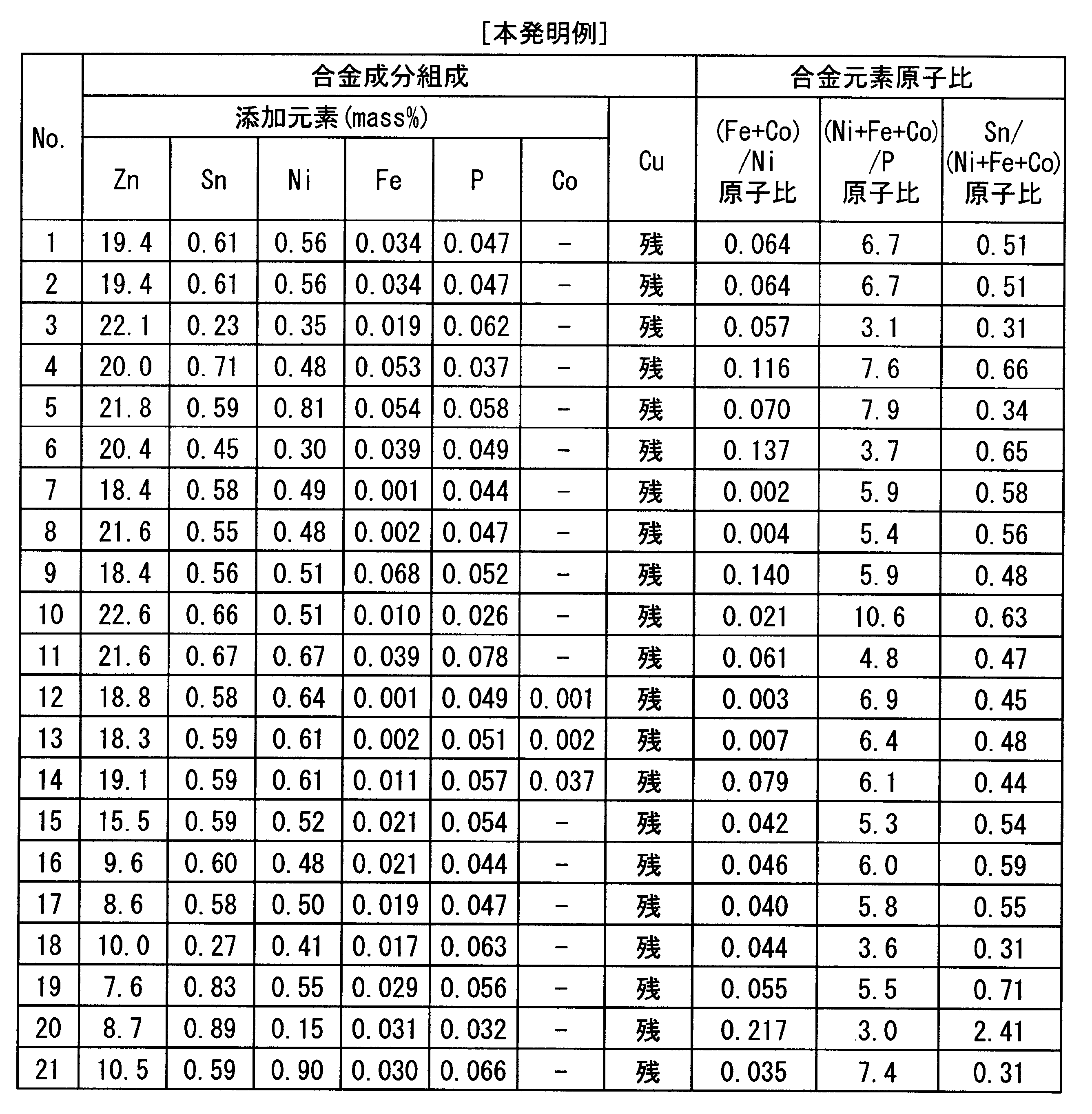
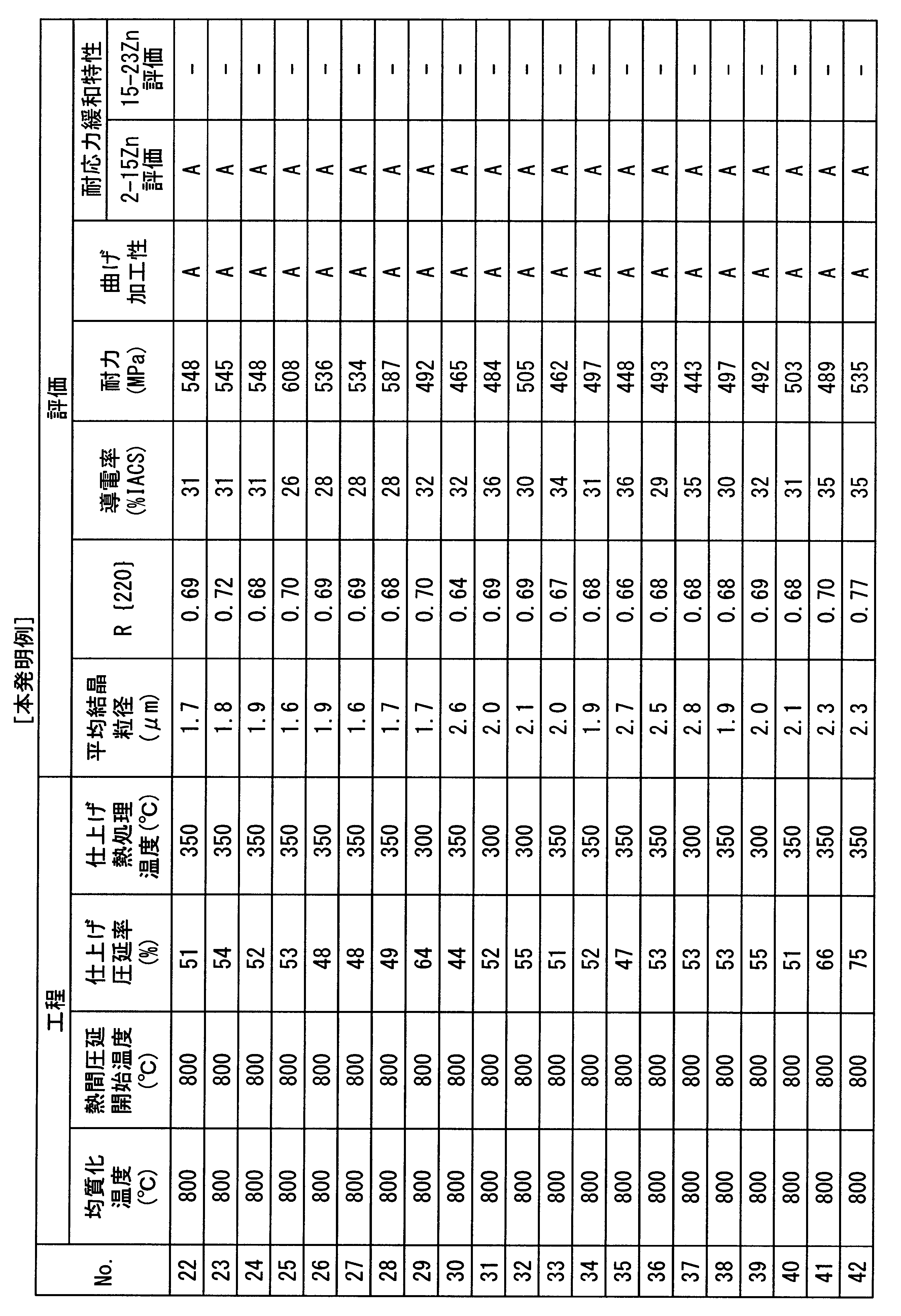
- No. Nos. 1 to 14 are examples of the present invention based on a Cu-20Zn alloy containing about 20% of Zn
- No. No. 15 is an example of the present invention based on a Cu-15Zn alloy containing about 15% Zn
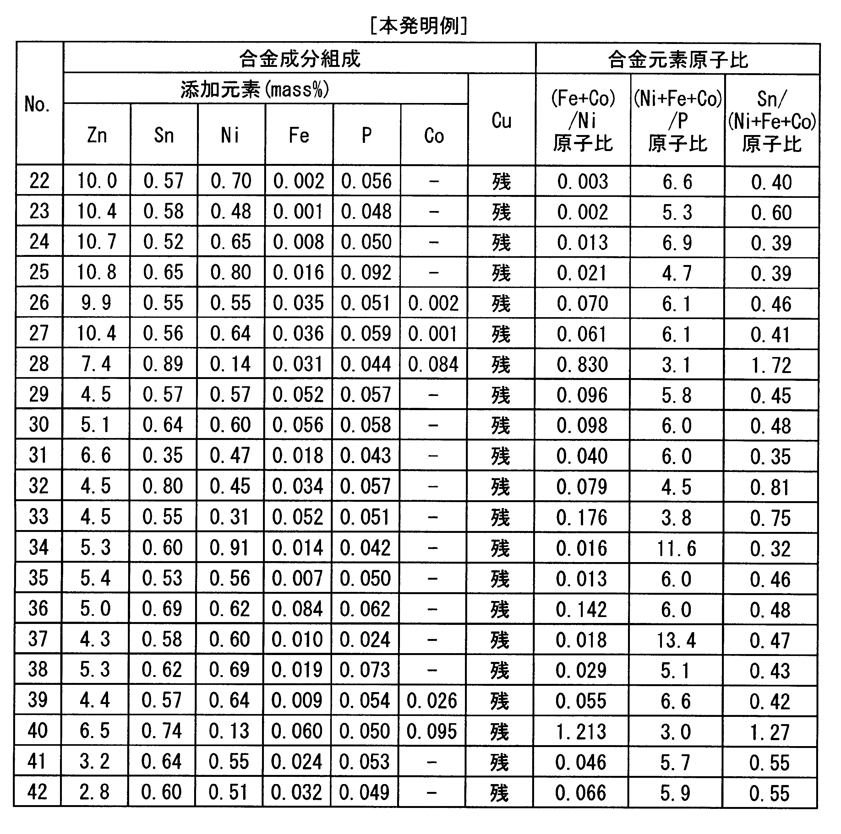
- No. 15 Nos. 16 to 28 are examples of the present invention based on a Cu-10Zn alloy containing about 10% of Zn
- No. Nos. 29 to 40 are examples of the present invention based on a Cu-5Zn alloy containing about 5% of Zn
- No. 41 and 42 are examples of the present invention based on a Cu-3Zn alloy containing about 3% Zn.
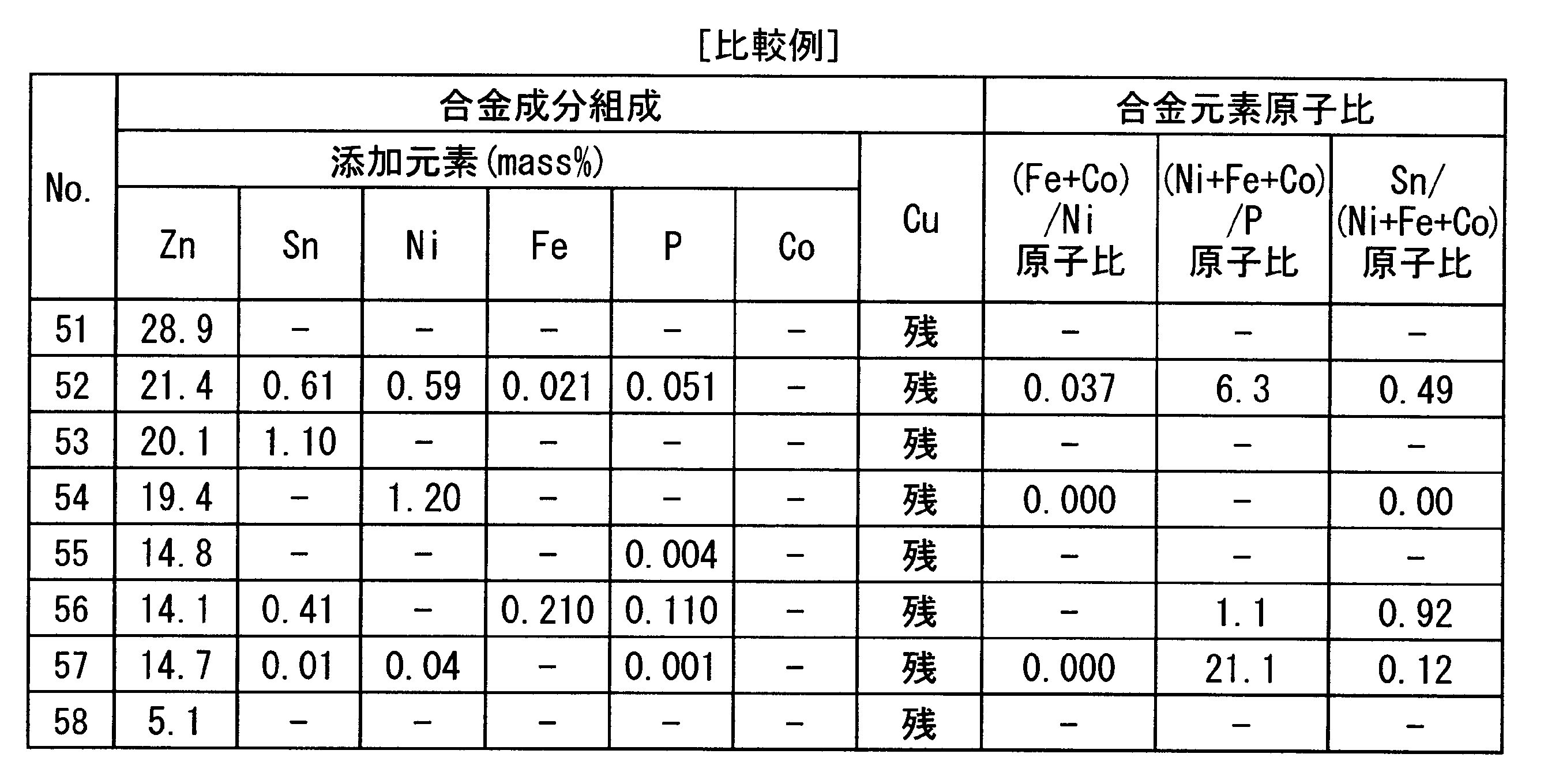
- No. No. 51 is a comparative example in which the Zn content exceeded the upper limit of the range of the present invention. Nos.
- 52 to 54 are comparative examples in which a Cu-20Zn alloy containing about 20% Zn is used as a base.
- Nos. 55 to 57 are comparative examples based on a Cu-15Zn alloy containing about 15% Zn
- 58 is a comparative example based on a Cu-5Zn alloy containing about 5% Zn.
- Comparative Example No. No. 51 is a Cu-30Zn alloy, which has poor stress relaxation resistance.
- Comparative Example No. No. 52 is a Cu-20Zn-based alloy in which the X-ray diffraction intensity ratio R ⁇ 220 ⁇ of the ⁇ 220 ⁇ plane on the plate surface is out of the scope of the present invention, which is higher than the Cu-20Zn-based alloy of the present invention example. Stress relaxation resistance and bending workability were inferior.
- Comparative Example No. No. 53 is a Cu-20Zn based alloy to which Ni, Fe and P are not added, and its stress relaxation resistance is inferior to that of the Cu-20Zn based alloy of the present invention. Comparative Example No. No.
- Comparative Example No. 54 is a Cu-20Zn-based alloy to which Sn, Fe, and P are not added, and its stress relaxation resistance is inferior to that of the Cu-20Zn-based alloy of the example of the present invention.
- Comparative Example No. No. 55 is a Cu-15Zn-based alloy to which Sn, Ni, and Fe are not added, and its stress relaxation resistance is inferior to that of the Cu-15Zn-based alloy of the present invention.
- Comparative Example No. No. 56 is a Cu-15Zn-based alloy in which Ni is not added and the P content is larger than the range of the present invention, which is more resistant to stress relaxation and bending than the Cu-15Zn-based alloy of the present invention. Workability was inferior. Comparative Example No.
- Comparative Example No. No. 58 is a Cu-5Zn alloy to which Sn, Ni, Fe and P are not added, and its stress relaxation resistance is inferior.
- the copper alloy of the present invention is easily thinned and has an excellent proof stress-bending balance, it can be used as a material for electronic / electric equipment parts that undergo severe bending. Moreover, since the copper alloy of this invention is excellent in stress relaxation resistance, it can maintain the contact pressure with the other member for components for electronic and electrical equipment over a long period of time.
- the present invention can provide such a copper alloy for electronic / electric equipment, a copper alloy thin plate using the same, a component for electronic / electric equipment, and a terminal.
Landscapes
- Chemical & Material Sciences (AREA)
- Engineering & Computer Science (AREA)
- Materials Engineering (AREA)
- Mechanical Engineering (AREA)
- Metallurgy (AREA)
- Organic Chemistry (AREA)
- Physics & Mathematics (AREA)
- Thermal Sciences (AREA)
- Crystallography & Structural Chemistry (AREA)
- Conductive Materials (AREA)
- Non-Insulated Conductors (AREA)
Abstract
Description
本願は、2012年12月28日に、日本に出願された特願2012-288052号に基づき優先権を主張し、その内容をここに援用する。
また、コネクタなどの端子の場合、相手側の導電部材との接触の信頼性を高めるため、Cu-Zn合金からなる基材(素板)の表面に錫(Sn)めっきを施して使用することがある。Cu-Zn合金を基材としてその表面にSnめっきを施したコネクタなどの導電部品においては、Snめっき材のリサイクル性を向上させるとともに、強度を向上させるため、Cu-Zn合金にさらにSnを添加し、Cu-Zn―Sn系合金を使用する場合がある。
特許文献1には、Cu-Zn―Sn系合金にNiを含有させてNi-P系化合物を生成させることによって耐応力緩和特性を向上させることができるとされ、またFeの添加も耐応力緩和特性の向上に有効であることが示されている。
特許文献2においては、Cu-Zn―Sn系合金に、Ni、FeをPとともに添加して化合物を生成させることにより、強度、弾性、耐熱性を向上させ得ることが記載されている。上記の強度、弾性、耐熱性の向上は、銅合金の耐応力緩和特性の向上を意味している。
さらに、リードフレーム材を対象とした特許文献4においては、Cu-Zn―Sn系合金に、Ni、FeをPとともに添加し、(Fe+Ni)/Pの原子比を0.2~3の範囲内に調整して、Fe―P系化合物、Ni―P系化合物、Fe―Ni―P系化合物を生成させることにより、耐応力緩和特性の向上が可能となる旨、記載されている。
また、特許文献3においては、Ni/Sn比を調整することが開示されているが、P化合物と耐応力緩和特性との関係については全く考慮されておらず、十分かつ確実な耐応力緩和特性の向上を図ることができなかった。
さらに、特許文献4においては、Fe、Ni、Pの合計量と、(Fe+Ni)/Pの原子比とを調整しただけであり、耐応力緩和特性の十分な向上を図ることができなかった。
そこで、耐応力緩和特性のより一層の確実かつ十分な改善が強く望まれている。
さらに、上記のNi、Fe、Pと同時に適量のCoを添加することにより、耐応力緩和特性および強度をより一層向上させることができることを見い出した。
なお、上記のX線回折強度は、銅合金母相のα相からのX線回折強度である。
なお、ここで〔Ni,Fe〕-P系析出物とは、Ni―Fe―Pの3元系析出物、あるいはFe―PもしくはNi―Pの2元系析出物であり、さらにこれらに他の元素、例えば主成分のCu、Zn、Sn、不純物のO、S、C、Co、Cr、Mo、Mn、Mg、Zr、Tiなどを含有した多元系析出物を含むことがある。また、この〔Ni,Fe〕-P系析出物は、リン化物、もしくはリンを固溶した合金の形態で存在する。
なお、上記のX線回折強度は、銅合金母相のα相からのX線回折強度である。
なお、上記第2の態様にかかる銅合金は、上記第1の態様にかかる銅合金であって、さらにCoを0.001mass%以上0.1mass%未満含有し、FeとCoの合計含有量とNiの含有量との比(Fe+Co)/Niが、原子比で、(Fe+Co)/Ni<1.5を満たし、Ni、FeおよびCoの合計含有量(Ni+Fe+Co)とPの含有量との比(Ni+Fe+Co)/Pが、原子比で、(Ni+Fe+Co)/P<15を満たし、Snの含有量とNi、FeおよびCoの合計含有量(Ni+Fe+Co)との比Sn/(Ni+Fe+Co)が、原子比で、0.3<Sn/(Ni+Fe+Co)を満たすものであってもよい。
なお、ここで〔Ni,Fe,Co〕-P系析出物とは、Ni―Fe―Co―Pの4元系析出物、あるいはNi-Fe―P、Ni―Co―P、もしくはFe-Co―Pの3元系析出物、あるいはFe―P、Ni-P、もしくはCo―Pの2元系析出物であり、さらにこれらに他の元素、例えば主成分のCu、Zn、Sn、不純物のO、S、C、Cr、Mo、Mn、Mg、Zr、Tiなどを含有した多元系析出物を含むことがある。また、この〔Ni,Fe,Co〕-P系析出物は、リン化物、もしくはリンを固溶した合金の形態で存在する。
上記第1または第2の態様にかかる電子・電気機器用銅合金においては、0.2%耐力が300MPa以上の機械特性を有することが好ましい。
このような0.2%耐力が300MPa以上の機械特性を有する電子・電気機器用銅合金は、例えば電磁リレーの可動導電片あるいは端子のバネ部のごとく、特に高強度が要求される導電部品に適している。
このような構成の電子・電気機器用銅合金薄板は、コネクタ、その他の端子、電磁リレーの可動導電片、リードフレームなどに好適に使用することができる。
上記の電子・電気機器用銅合金薄板は、薄板本体の表面において、母相(α相)の{111}面からのX線回折強度、{200}面からのX線回折強度、{220}面からのX線回折強度、{311}面からのX線回折強度が、上記第1または第2の態様に記載される条件R{220}=I{220}/(I{111}+I{200}+I{220}+I{311})を満足するものとすることができる。
この場合、Snめっきの下地の基材は0.1mass%以上0.9mass%以下のSnを含有するCu-Zn―Sn系合金で構成されているため、使用済みのコネクタなどの部品をSnめっきCu-Zn系合金のスクラップとして回収して良好なリサイクル性を確保することができる。
本発明の第5の態様は、電子・電気機器用導電部品であって、上述の電子・電気機器用銅合金薄板からなることを特徴とする。
なお、本発明における電子・電気機器用導電部品とは、端子、コネクタ、リレー、リードフレーム等を含むものである。
さらに、本発明の第7の態様にかかる端子は、上述の電子・電気機器用銅合金薄板からなることを特徴とする。
なお、本発明における端子は、コネクタ等を含むものである。
本実施形態である電子・電気機器用銅合金は、Znを2mass%超えて23mass%未満、Snを0.1mass%以上0.9mass%以下、Niを0.05mass%以上1.0mass%未満、Feを0.001mass%以上0.10mass%未満、Pを0.005mass%以上0.1mass%以下含有し、残部がCuおよび不可避的不純物からなる組成を有する。
0.002≦Fe/Ni<1.5 ・・・(1)
を満たし、かつNiの含有量およびFeの含有量の合計量(Ni+Fe)とPの含有量との比(Ni+Fe)/Pが、原子比で、次の(2)式
3<(Ni+Fe)/P<15 ・・・(2)
を満たし、さらにSnの含有量とNiの含有量およびFeの含有量の合計量(Ni+Fe)との比Sn/(Ni+Fe)が、原子比で、次の(3)式
0.3<Sn/(Ni+Fe)<5 ・・・(3)
を満たすように定められている。
そして、各合金元素の相互間の含有量比率として、FeおよびCoの合計含有量とNiの含有量との比(Fe+Co)/Niが、原子比で、次の(1´)式
0.002≦(Fe+Co)/Ni<1.5 ・・・(1´)
を満たし、さらにNi、FeおよびCoの合計含有量(Ni+Fe+Co)とPの含有量との比(Ni+Fe+Co)/Pが、原子比で、次の(2´)式
3<(Ni+Fe+Co)/P<15 ・・・(2´)
を満たし、さらにSnの含有量とNi、FeおよびCoの合計含有量(Ni+Fe+Co)との比Sn/(Ni+Fe+Co)が、原子比で、次の(3´)式
0.3<Sn/(Ni+Fe+Co)<5 ・・・(3´)
を満たすように定められている。
なお、上記の(1)、(2)、(3)式を満足する銅合金であって、さらにCoを0.001mass%以上、0.10mass%未満含有し、FeとCoの合計含有量とNiの含有量との比(Fe+Co)/Niが、原子比で、(Fe+Co)/Ni<1.5を満たし、Ni、FeおよびCoの合計含有量(Ni+Fe+Co)とPの含有量との比(Ni+Fe+Co)/Pが、原子比で、(Ni+Fe+Co)/P<15を満たし、Snの含有量とNi、FeおよびCoの合計含有量(Ni+Fe+Co)との比Sn/(Ni+Fe+Co)が、原子比で、0.3<Sn/(Ni+Fe+Co)を満たす場合には、上記の(1´)式、(2´)式、(3´)式も満足される。
Znは、本実施形態で対象としている銅合金において基本的な合金元素であり、強度およびばね性の向上に有効な元素である。また、ZnはCuより安価であるため、銅合金の材料コストの低減にも効果がある。Znが2mass%以下では、材料コストの低減効果が十分に得られない。一方、Znが23mass%以上では、耐食性が低下するとともに、銅合金の冷間圧延性も低下してしまう。
そこで、本実施形態では、Znの含有量を2mass%超え23mass%未満の範囲内とした。なお、Znの含有量は、上記の範囲内でも2mass%超え15mass%以下の範囲内が好ましく、さらには3mass%以上15mass%以下の範囲内が好ましい。
Snの添加は銅合金の強度向上に効果があり、Snめっき付きCu-Zn合金材のリサイクル性の向上に有利となる。さらに、SnがNiおよびFeと共存すれば、銅合金の耐応力緩和特性の向上にも寄与することが本発明者等の研究により判明している。Snが0.1mass%未満ではこれらの効果が十分に得られず、一方、Snが0.9mass%を超えれば、熱間加工性および冷間圧延性が低下し、銅合金の熱間圧延や冷間圧延で割れが発生してしまうおそれがあり、導電率も低下してしまう。
そこで、本実施形態では、Snの含有量を0.1mass%以上0.9mass%以下の範囲内とした。なお、Snの含有量は、上記の範囲内でも特に0.2mass%以上0.8mass%以下の範囲内が好ましい。
Niは、Fe、Pとともに添加することにより、〔Ni,Fe〕-P系析出物を銅合金の母相(α相主体)から析出させることができ、また、Fe、Co,Pとともに添加することにより、〔Ni,Fe,Co〕-P系析出物を母相(α相主体)から析出させることができる。これら〔Ni,Fe〕-P系析出物もしくは〔Ni,Fe,Co〕-P系析出物によって再結晶の際に結晶粒界をピン止めする効果により、平均結晶粒径を小さくすることができ、銅合金の強度、曲げ加工性、耐応力腐食割れ性を向上させることができる。さらに、これらの析出物の存在により、銅合金の耐応力緩和特性を大幅に向上させることができる。加えて、NiをSn、Fe、Co,Pと共存させることで、固溶強化によっても銅合金の耐応力緩和特性を向上させることができる。ここで、Niの添加量が0.05mass%未満では、耐応力緩和特性を十分に向上させることができない。一方、Niの添加量が1.0mass%以上となれば、固溶Niが多くなって導電率が低下し、また高価なNi原材料の使用量の増大によりコスト上昇を招く。
そこで、本実施形態では、Niの含有量を0.05mass%以上1.0mass%未満の範囲内とした。なお、Niの含有量は、上記の範囲内でも特に0.2mass%以上、0.8mass%未満の範囲内とすることが好ましい。
Feは、Ni、Pとともに添加することにより、〔Ni,Fe〕-P系析出物を銅合金の母相(α相主体)から析出させることができ、また、Ni、Co,Pとともに添加することにより、〔Ni,Fe,Co〕-P系析出物を銅合金の母相(α相主体)から析出させることができる。これら〔Ni,Fe〕-P系析出物もしくは〔Ni,Fe,Co〕-P系析出物によって再結晶の際に結晶粒界をピン止めする効果により、平均結晶粒径を小さくすることができ、銅合金の強度、曲げ加工性、耐応力腐食割れ性を向上させることができる。さらに、これらの析出物の存在により、銅合金の耐応力緩和特性を大幅に向上させることができる。ここで、Feの添加量が0.001mass%未満では、結晶粒界をピン止めする効果が十分に得られず、十分な強度が得られない。一方、Feの添加量が0.10mass%以上となれば、一層の強度向上は認められず、固溶Feが多くなって銅合金の導電率が低下し、また冷間圧延性も低下してしまう。
そこで、本実施形態では、Feの含有量を0.001mass%以上0.10mass%未満の範囲内とした。なお、Feの含有量は、上記の範囲内でも特に0.002mass%以上0.08mass%以下の範囲内とすることが好ましい。
Coは、必ずしも必須の添加元素ではないが、少量のCoをNi、Fe、Pとともに添加すれば、〔Ni,Fe,Co〕-P系析出物が生成され、銅合金の耐応力緩和特性をより一層向上させることができる。ここで、Co添加量が0.001mass%未満では、Co添加による耐応力緩和特性のより一層の向上効果が得られない。一方、Co添加量が0.10mass%以上となれば、固溶Coが多くなって銅合金の導電率が低下し、また高価なCo原材料の使用量の増大によりコスト上昇を招く。
そこで、本実施形態では、Coを添加する場合に、Coの含有量を0.001mass%以上0.10mass%未満の範囲内とした。Coの含有量は、上記の範囲内でも特に0.002mass%以上0.08mass%以下の範囲内とすることが好ましい。なお、Coを積極的に添加しない場合でも、不純物として0.001mass%未満のCoが含有されることがある。
Pは、Fe、Ni、さらにはCoとの結合性が高く、Fe、Niとともに適量のPを含有させれば、〔Ni,Fe〕-P系析出物を析出させることができ、またFe、Ni、Coとともに適量のPを含有させれば、〔Ni,Fe,Co〕-P系析出物を析出させることができ、そしてこれらの析出物の存在によって銅合金の耐応力緩和特性を向上させることができる。ここで、P量が0.005mass%未満では、十分に〔Ni,Fe〕-P系析出物または〔Ni,Fe,Co〕-P系析出物を析出させることが困難となり、十分に銅合金の耐応力緩和特性を向上させることができなくなる。一方、P量が0.10mass%を超えれば、P固溶量が多くなって、導電率が低下するとともに圧延性が低下して冷間圧延割れが生じやすくなってしまう。
そこで、本実施形態では、Pの含有量を0.005mass%以上0.10mass%以下の範囲内とした。Pの含有量は、上記の範囲内でも特に0.01mass%以上0.08mass%以下の範囲内が好ましい。
なお、Pは、銅合金の溶解原料から不可避的に混入することが多い元素であり、従ってP量を上述のように規制するためには、溶解原料を適切に選定することが望ましい。
本発明者等らは、詳細な実験の結果、Fe、Niのそれぞれの含有量を前述のように調整するだけではなく、それらの比Fe/Niを、原子比で、0.002以上、1.5未満の範囲内とした場合に、十分な耐応力緩和特性の向上を図り得ることを見い出した。ここで、Fe/Ni比が1.5以上の場合、銅合金の耐応力緩和特性が低下する。Fe/Ni比が0.002未満の場合、銅合金の強度が低下するとともに高価なNiの原材料使用量が相対的に多くなってコスト上昇を招く。そこで、Fe/Ni比は、上記の範囲内に規制することとした。
なお、Fe/Ni比は、上記の範囲内でも、特に0.005以上1以下の範囲内が望ましく、0.005以上0.5以下がさらに望ましい。
(Ni+Fe)/P比が3以下では、固溶Pの割合の増大に伴って銅合金の耐応力緩和特性が低下し、また同時に固溶Pにより導電率が低下するとともに、圧延性が低下して冷間圧延割れが生じやすくなり、さらに曲げ加工性も低下する。一方、(Ni+Fe)/P比が15以上となれば、固溶したNi、Feの割合の増大により銅合金の導電率が低下するとともに高価なNiの原材料使用量が相対的に多くなってコスト上昇を招く。そこで、(Ni+Fe)/P比を上記の範囲内に規制することとした。なお、(Ni+Fe)/P比は、上記の範囲内でも、特に3を超え、12以下の範囲内が望ましい。
Sn/(Ni+Fe)比が0.3以下では、十分な耐応力緩和特性向上効果が発揮されず、一方Sn/(Ni+Fe)比が5以上の場合、相対的に(Ni+Fe)量が少なくなって、〔Ni,Fe〕-P系析出物の量が少なくなり、銅合金の耐応力緩和特性が低下してしまう。そこで、Sn/(Ni+Fe)比を上記の範囲内に規制することとした。なお、Sn/(Ni+Fe)比は、上記の範囲内でも、特に0.3を超え、2.5以下の範囲内が望ましく、さらには0.3を超え、1.5以下の範囲内が望ましい。
Coを添加した場合、Feの一部をCoで置き換えたと考えればよく、(1´)式も基本的には(1)式に準じている。ここで、(Fe+Co)/Ni比が1.5以上の場合には、銅合金の耐応力緩和特性が低下するとともに高価なCo原材料の使用量の増大によりコスト上昇を招く。(Fe+Co)/Ni比が0.002未満の場合には、銅合金の強度が低下するとともに高価なNiの原材料使用量が相対的に多くなってコスト上昇を招く。そこで、(Fe+Co)/Ni比は、上記の範囲内に規制することとした。なお、(Fe+Co)/Ni比は、上記の範囲内でも、特に0.005以上1以下の範囲内が望ましく、0.005以上0.5以下がさらに望ましい。
Coを添加する場合の(2´)式も、前記(2)式に準じている。(Ni+Fe+Co)/P比が3以下では、固溶Pの割合の増大に伴って耐応力緩和特性が低下し、また同時に固溶Pにより銅合金の導電率が低下するとともに、圧延性が低下して冷間圧延割れが生じやすくなり、さらに曲げ加工性も低下する。一方、(Ni+Fe+Co)/P比が15以上となれば、固溶したNi、Fe、Coの割合の増大により銅合金の導電率が低下するとともに高価なCoやNiの原材料使用量が相対的に多くなってコスト上昇を招く。そこで、(Ni+Fe+Co)/P比を上記の範囲内に規制することとした。なお、(Ni+Fe+Co)/P比は、上記の範囲内でも、特に3を超え、12以下の範囲内が望ましい。
Coを添加する場合の(3´)式も、前記(3)式に準じている。Sn/(Ni+Fe+Co)比が0.3以下では、十分な耐応力緩和特性向上効果が発揮されず、一方、Sn/(Ni+Fe+Co)比が5以上となれば、相対的に(Ni+Fe+Co)量が少なくなって、〔Ni,Fe,Co〕-P系析出物の量が少なくなり、銅合金の耐応力緩和特性が低下してしまう。そこで、Sn/(Ni+Fe+Co)比を上記の範囲内に規制することとした。なお、Sn/(Ni+Fe+Co)比は、上記の範囲内でも、特に0.3を超え、2.5以下の範囲内が望ましく、さらには0.3を超え、1.5以下の範囲内が望ましい。
すなわち、一板表面における{111}面からのX線回折強度をI{111}、
{200}面からのX線回折強度をI{200}、
{220}面からのX線回折強度をI{220}、
{311}面からのX線回折強度をI{311}、
{220}面からのX線回折強度の割合R{220}を
R{220}=I{220}/(I{111}+I{200}+I{220}+I{311})とした場合に、R{220}が0.8以下とされているように構成している。
ここで、上述のように、一板表面におけるX回折強度比を規定した理由について以下に説明する。
表面(例えば、板材の板表面)における{220}面は、圧延集合組織によるものであり、この{220}面の割合が高くなると、圧延方向に対して垂直方向に曲げ加工を行った場合に、曲げ加工の応力方向に対して滑り系が活動しにくい方位関係となる。これにより、曲げ加工時に変形が局所的に発生し、クラックの原因となる。
このため、一表面における{220}面からのX線回折強度の割合R{220}を0.8以下に抑制することにより、クラックの発生を抑制でき、曲げ加工性が向上するものと考えられる。ここで、{220}面からのX線回折強度の割合R{220}は、上記の範囲内でも0.7以下が好ましい。
なお、{220}面からのX線回折強度の割合R{220}の下限には、特に規定はないが、0.3以上とすることが好ましい。
まず、前述した成分組成の銅合金溶湯を溶製する。銅原料としては、純度が99.99%以上の4NCu(無酸素銅等)を使用することが望ましいが、スクラップを原料として用いてもよい。また、溶解には、大気雰囲気炉を用いてもよいが、添加元素の酸化を抑制するために、真空炉、不活性ガス雰囲気又は還元性雰囲気とされた雰囲気炉を用いてもよい。
次いで、成分調整された銅合金溶湯を、適宜の鋳造法、例えば金型鋳造などのバッチ式鋳造法、あるいは連続鋳造法、半連続鋳造法などによって鋳造して鋳塊を得る。
その後、必要に応じて、鋳塊の偏析を解消して鋳塊組織を均一化するために均質化熱処理を行う。または晶出物、析出物を固溶させるために溶体化熱処理を行う。この熱処理の条件は特に限定しないが、通常は600~1000℃において1秒~24時間加熱すればよい。熱処理温度が600℃未満、あるいは熱処理時間が5分未満では、十分な均質化効果または溶体化効果が得られないおそれがある。一方、熱処理温度が1000℃を超えれば、偏析部位が一部溶解してしまうおそれがあり、さらに熱処理時間が24時間を超えることはコスト上昇を招くだけである。熱処理後の冷却条件は、適宜定めればよいが、通常は水焼入れすればよい。なお、熱処理後には、必要に応じて面削を行う。
次いで、粗加工の効率化と組織の均一化のために、鋳塊に対して熱間加工を行ってもよい。この熱間加工の条件は特に限定されないが、通常は、開始温度600~1000℃、終了温度300~850℃、加工率10~99%程度とすることが好ましい。なお、熱間加工開始温度までの鋳塊加熱は、前述の加熱工程S02と兼ねてもよい。熱間加工後の冷却条件は、適宜定めればよいが、通常は水焼入れすればよい。なお、熱間加工後には、必要に応じて面削を行う。熱間加工の加工方法については、特に限定されないが、最終形状が板や条の場合は熱間圧延を適用すればよい。また最終形状が線や棒の場合には、押出や溝圧延を、また最終形状がバルク形状の場合には、鍛造やプレスを適用すればよい。
次に、加熱工程S02で均質化処理を施した鋳塊、あるいは熱間圧延などの熱間加工S03を施した熱間加工材に対して、中間塑性加工を施す。この中間塑性加工S04における温度条件は特に限定はないが、冷間又は温間加工となる-200℃から+200℃の範囲内とすることが好ましい。中間塑性加工の加工率も特に限定されないが、通常は10~99%程度とする。加工方法は特に限定されないが、最終形状が板、条の場合は、圧延を適用すればよい。また最終形状が線や棒の場合には、押出や溝圧延、さらに最終形状がバルク形状の場合には、鍛造やプレスを適用する事ができる。なお、溶体化の徹底のために、S02~S04を繰り返してもよい。
冷間もしくは温間での中間塑性加工S04の後に、再結晶処理と析出処理を兼ねた中間熱処理を施す。この中間熱処理は、組織を再結晶させると同時に、〔Ni,Fe〕-P系析出物もしくは〔Ni,Fe,Co〕-P系析出物を分散析出させるために実施される工程であり、これらの析出物が生成される加熱温度、加熱時間の条件を適用すればよく、通常は、200~800℃で、1秒~24時間とすればよい。但し、結晶粒径は、耐応力緩和特性にある程度の影響を与えるから、中間熱処理による再結晶粒を測定して、加熱温度、加熱時間の条件を適切に選択することが望ましい。なお、中間熱処理およびその後の冷却は、最終的な平均結晶粒径に影響を与えるから、これらの条件は、α相の平均結晶粒径が0.1~50μmの範囲内となるように選定することが望ましい。
中間熱処理後の冷却条件は、特に限定しないが、通常は2000℃/秒~100℃/時間程度の冷却速度で冷却すればよい。
なお、必要に応じて、上記の中間塑性加工S04と中間熱処理工程S05を、複数回繰り返してもよい。
中間熱処理工程S05の後には、最終寸法、最終形状まで仕上げ加工を行う。仕上げ塑性加工における加工方法は特に限定されないが、最終製品形態が板や条である場合には、圧延(冷間圧延)を適用すればよい。その他、最終製品形態に応じて、鍛造やプレス、溝圧延などを適用してもよい。加工率は最終板厚や最終形状に応じて適宜選択すればよいが、1~99%、特に1~70%の範囲内が好ましい。加工率が1%未満では、耐力を向上させる効果が十分に得られず、一方70%を超えれば、実質的に再結晶組織が失われて加工組織となり、曲げ加工性が低下してしまうおそれがある。なお、加工率は、好ましくは1~70%、より好ましくは、5~70%とする。仕上げ塑性加工後は、これをそのまま製品として用いてもよいが、通常は、さらに仕上げ熱処理を施すことが好ましい。
仕上げ塑性加工後には、必要に応じて、耐応力緩和特性の向上および低温焼鈍硬化のために、または残留ひずみの除去のために、仕上げ熱処理工程S07を行う。この仕上げ熱処理は、50~800℃の範囲内の温度で、0.1秒~24時間行うことが望ましい。仕上げ熱処理の温度が50℃未満、または仕上げ熱処理の時間が0.1秒未満では、十分な歪み取りの効果が得られなくなるおそれがあり、一方、仕上げ熱処理の温度が800℃を超える場合は再結晶のおそれがあり、さらに仕上げ熱処理の時間が24時間を超えることは、コスト上昇を招くだけである。なお、仕上げ塑性加工S06を行わない場合には、仕上げ熱処理工程S07は省略してもよい。
また、加工方法として圧延を適用した場合、板厚0.05~1.0mm程度の電子・電気機器用銅合金薄板(条材)を得ることができる。このような薄板は、これをそのまま電子・電気機器用導電部品に使用してもよいが、板面の一方、もしくは両面に、膜厚0.1~10μm程度のSnめっきを施し、Snめっき付き銅合金条として、コネクタその他の端子などの電子・電気機器用導電部品に使用するのが通常である。この場合のSnめっきの方法は特に限定されない。また、場合によっては電解めっき後にリフロー処理を施してもよい。
また、表面にSnめっきを施した場合には、使用済みのコネクタなどの部品をSnめっきCu-Zn系合金のスクラップとして回収して良好なリサイクル性を確保することができる。
例えば、製造方法の一例を挙げて説明したが、これに限定されることはなく、最終的に得られた電子・電気機器用銅合金が、本発明の範囲内の組成であり、かつ、一表面における{220}面からのX線回折強度の割合R{220}を0.8以下に設定されていればよい。
続いて各鋳塊について、均質化処理(加熱工程S02)として、Arガス雰囲気中において、800℃で所定時間保持後、水焼き入れを実施した。
具体的には、中間塑性加工および中間熱処理をそれぞれ1回実施する場合には、圧延率約90%以上の冷間圧延(中間塑性加工)を行った後、再結晶と析出処理のための中間熱処理として、200~800℃で、所定時間の熱処理を実施し、水焼入れした。その後、圧延材を切断し、酸化被膜を除去するために表面研削を実施した。
一方、中間塑性加工および中間熱処理をそれぞれ2回実施する場合には、圧延率約50~90%の一次冷間圧延(一次中間塑性加工)を行った後、一次中間熱処理として、200~800℃で所定時間の熱処理を実施して水焼入れした後、圧延率約50~90%の二次冷間圧延(二次中間塑性加工)を施し、200~800℃の間で所定の時間の二次中間熱処理を実施し、水焼入れした。その後、圧延材を切断し、酸化被膜を除去するために表面研削を実施した。
最後に、150~400℃で仕上げ熱処理を実施した後、水焼入れし、切断および表面研磨を実施した後、厚さ0.25mm×幅約160mmの特性評価用条材を製出した。
また、平均結晶粒径10μm以下の場合は、圧延の幅方向に対して垂直な面、すなわちTD面(Transverse direction)を観察面として、EBSD測定装置及びOIM解析ソフトによって、次のように結晶粒界および結晶方位差分布を測定した。
耐水研磨紙、ダイヤモンド砥粒を用いて機械研磨を行った後、コロイダルシリカ溶液を用いて仕上げ研磨を行った。そして、EBSD測定装置(FEI社製Quanta FEG 450,EDAX/TSL社製(現 AMETEK社) OIM Data Collection)と、解析ソフト(EDAX/TSL社製(現 AMETEK社)OIM Data Analysis ver.5.3)によって、電子線の加速電圧20kV、測定間隔0.1μmステップで1000μm2以上の測定面積で、各結晶粒の方位差の解析を行った。解析ソフトOIMにより各測定点のCI値(Confidence Index)を計算し、結晶粒径の解析からはCI値が0.1以下のものは除外した。結晶粒界は、二次元断面観察の結果、隣り合う2つの結晶間の配向方位差が15°以上となる測定点間を大傾角粒界とし、2°以上15°以下を小傾角粒界とした。大傾角粒界を用いて、結晶粒界マップを作成し、JIS H 0501の切断法に準拠し、結晶粒界マップに対して、縦、横の所定長さの線分を5本ずつ引き、完全に切られる結晶粒数を数え、その切断長さの平均値を平均結晶粒径とした。なお、本実施例では、平均結晶粒径は、α相の結晶粒について規定している。上記の平均結晶粒径測定にあたっては、α相以外のβ相などの結晶はほとんど存在しなかったが、存在した場合は除外して平均粒径を算出している。
条材表面における{111}面からのX線回折強度をI{111}、{200}面からのX線回折強度I{200}、{220}面からのX線回折強度I{220}、{311}面からのX線回折強度I{311}は、次のような手順で測定する。特性評価用条材から測定試料を採取し、反射法で、測定試料に対して1つの回転軸の回りのX線回折強度を測定した。ターゲットにはCuを使用し、KαのX線を使用した。管電流40mA、管電圧40kV、測定角度40~150°、測定ステップ0.02°の条件で測定し、回折角とX線回折強度のプロファイルにおいて、X線回折強度のバックグラウンドを除去後、各回折面からのピークのKα1とKα2を合わせた積分X線回折強度Iを求め、以下の式、
R{220}=I{220}/(I{111}+I{200}+I{220}+I{311})
より、R{220}の値を求めた。
特性評価用条材からJIS Z 2201に規定される13B号試験片を採取し、JIS Z 2241のオフセット法により、0.2%耐力σ0.2を測定した。なお、試験片は、引張試験の引張方向が特性評価用条材の圧延方向に対して直交する方向となるように採取した。
特性評価用条材から幅10mm×長さ60mmの試験片を採取し、4端子法によって電気抵抗を求めた。また、マイクロメータを用いて試験片の寸法測定を行い、試験片の体積を算出した。そして、測定した電気抵抗値と体積とから、導電率を算出した。なお、試験片は、その長手方向が特性評価用条材の圧延方向に対して平行になるように採取した。
JCBA(日本伸銅協会技術標準)T307-2007の4試験方法に準拠して曲げ加工を行った。曲げの軸が圧延方向に平行になるようにW曲げした。特性評価用条材から幅10mm×長さ30mm×厚さ0.25mmの試験片を複数採取し、曲げ角度が90度、曲げ半径が0.25mmのW型の治具を用い、W曲げ試験を行った。それぞれ3つのサンプルで割れ試験を実施し、各サンプルの4つの視野においてクラックが観察されなかったものをAで、1つの視野以上でクラックが観察されたものをBで示した。
耐応力緩和特性試験は、日本伸銅協会技術標準JCBA-T309:2004の片持はりねじ式に準じた方法によって応力を負荷し、下記に示す条件(温度、時間)で保持した後の残留応力率を測定した。
試験方法としては、各特性評価用条材から圧延方向に対して直交する方向に試験片(幅10mm)を採取し、試験片の表面最大応力が耐力の80%となるよう、初期たわみ変位を2mmと設定し、スパン長さを調整した。上記表面最大応力は次式で定められる。
表面最大応力(MPa)=1.5Etδ0/Ls 2ただし、
E:たわみ係数(MPa)
t:試料の厚み(t=0.25mm)
δ0:初期たわみ変位(2mm)
Ls:スパン長さ(mm)
である。
残留応力率(%)=(1-δt/δ0)×100ただし、
δt:120℃、もしくは150℃で1000h保持後の永久たわみ変位(mm)-常温で24h保持後の永久たわみ変位(mm)
δ0:初期たわみ変位(mm)
である。
残留応力率が、70%以上のものを良(A)、70%未満ものを不良(B)と評価した。
また、No.51は、Znの含有量が本発明範囲の上限を越えた比較例であり、さらに、No.52~54は、20%前後のZnを含有するCu-20Zn合金をベースとする比較例、No.55~57は、15%前後のZnを含有するCu-15Zn合金をベースとする比較例、No.58は、5%前後のZnを含有するCu-5Zn合金をベースとする比較例である。


比較例No.52は、板表面における{220}面のX線回折強度比R{220}が本発明の範囲外とされたCu-20Znベースの合金であり、本発明例のCu-20Znベースの合金よりも耐応力緩和特性及び曲げ加工性が劣っていた。
比較例No.53は、Ni、Fe、Pを添加しなかったCu-20Znベースの合金であり、本発明例のCu-20Znベースの合金よりも耐応力緩和特性が劣っていた。
比較例No.54は、Sn、Fe、Pを添加しなかったCu-20Znベースの合金であり、本発明例のCu-20Znベースの合金よりも耐応力緩和特性が劣っていた。
比較例No.55は、Sn、Ni、Feを添加しなかったCu-15Znベースの合金であり、本発明例のCu-15Znベースの合金よりも耐応力緩和特性が劣っていた。
比較例No.56は、Niを添加せず、Pの含有量が本発明の範囲よりも多くされたCu-15Znベースの合金であり、本発明例のCu-15Znベースの合金よりも耐応力緩和特性、曲げ加工性が劣っていた。
比較例No.57は、Feを添加せず、Pの含有量が本発明の範囲よりも少なくされたCu-15Znベースの合金であり、本発明例のCu-15Znベースの合金よりも耐応力緩和特性が劣っていた。
比較例No.58は、Sn、Ni、Fe、Pを添加しなかったCu-5Zn合金であって、耐応力緩和特性が劣っていた。
Claims (16)
- Znを2mass%超えて23mass%未満、Snを0.1mass%以上0.9mass%以下、Niを0.05mass%以上1.0mass%未満、Feを0.001mass%以上0.10mass%未満、Pを0.005mass%以上0.1mass%以下含有し、残部がCuおよび不可避的不純物からなり、
Feの含有量とNiの含有量との比Fe/Niが、原子比で、
0.002≦Fe/Ni<1.5
を満たし、
NiおよびFeの合計含有量(Ni+Fe)とPの含有量との比(Ni+Fe)/Pが、原子比で、
3<(Ni+Fe)/P<15
を満たし、
Snの含有量とNiおよびFeの合計量(Ni+Fe)との比Sn/(Ni+Fe)が、原子比で、
0.3<Sn/(Ni+Fe)<5
を満たすとともに、
一表面における{111}面からのX線回折強度をI{111}、
{200}面からのX線回折強度をI{200}、
{220}面からのX線回折強度をI{220}、
{311}面からのX線回折強度をI{311}、
{220}面からのX線回折強度の割合R{220}を
R{220}=I{220}/(I{111}+I{200}+I{220}+I{311})とした場合に、
R{220}が0.8以下とされている電子・電気機器用銅合金。 - Znを2mass%超えて23mass%未満、Snを0.1mass%以上0.9mass%以下、Niを0.05mass%以上1.0mass%未満、Feを0.001mass%以上0.10mass%未満、Coを0.001mass%以上0.1mass%未満、Pを0.005mass%以上0.1mass%以下含有し、残部がCuおよび不可避的不純物からなり、
FeとCoの合計含有量とNiの含有量との比(Fe+Co)/Niが、原子比で、
0.002≦(Fe+Co)/Ni<1.5
を満たし、
Ni、FeおよびCoの合計含有量(Ni+Fe+Co)とPの含有量との比(Ni+Fe+Co)/Pが、原子比で、
3<(Ni+Fe+Co)/P<15
を満たし、
Snの含有量とNi、FeおよびCoの合計含有量(Ni+Fe+Co)との比Sn/(Ni+Fe+Co)が、原子比で、
0.3<Sn/(Ni+Fe+Co)<5
を満たすとともに、
一表面における{111}面からのX線回折強度をI{111}、
{200}面からのX線回折強度をI{200}、
{220}面からのX線回折強度をI{220}、
{311}面からのX線回折強度をI{311}、
{220}面からのX線回折強度の割合R{220}を
R{220}=I{220}/(I{111}+I{200}+I{220}+I{311})とした場合に、
R{220}が0.8以下とされている電子・電気機器用銅合金。 - 請求項1に記載の電子・電気機器用銅合金において、前記R{220}が0.3以上0.8以下とされている電子・電気機器用銅合金。
- 請求項2に記載の電子・電気機器用銅合金において、前記R{220}が0.3以上0.8以下とされている電子・電気機器用銅合金。
- 請求項1に記載の電子・電気機器用銅合金において、0.2%耐力が300MPa以上の機械特性を有する電子・電気機器用銅合金。
- 請求項2に記載の電子・電気機器用銅合金において、0.2%耐力が300MPa以上の機械特性を有する電子・電気機器用銅合金。
- 請求項3に記載の電子・電気機器用銅合金において、0.2%耐力が300MPa以上の機械特性を有する電子・電気機器用銅合金。
- 請求項4に記載の電子・電気機器用銅合金において、0.2%耐力が300MPa以上の機械特性を有する電子・電気機器用銅合金。
- 請求項1から請求項8のいずれか一項に記載の電子・電気機器用銅合金の圧延材からなる薄板本体を有し、前記薄板本体の厚みが0.05mm以上1.0mm以下の範囲内にある電子・電気機器用銅合金薄板。
- 請求項9に記載の電子・電気機器用銅合金薄板において、さらに前記薄板本体の表面上に形成されたSnめっき層を有する、電子・電気機器用銅合金薄板。
- 請求項1から請求項8のいずれか一項に記載の電子・電気機器用銅合金からなる電子・電気機器用導電部品。
- 請求項1から請求項8のいずれか一項に記載の電子・電気機器用銅合金からなるこ端子。
- 請求項9に記載の電子・電気機器用銅合金薄板からなる電子・電気機器用導電部品。
- 請求項10に記載の電子・電気機器用銅合金薄板からなる電子・電気機器用導電部品。
- 請求項9に記載の電子・電気機器用銅合金薄板からなる端子。
- 請求項10に記載の電子・電気機器用銅合金薄板からなる端子。
Priority Applications (4)
| Application Number | Priority Date | Filing Date | Title |
|---|---|---|---|
| CN201380067756.1A CN104870672B (zh) | 2012-12-28 | 2013-06-28 | 电子电气设备用铜合金、电子电气设备用铜合金薄板、电子电气设备用导电元件及端子 |
| US14/758,032 US20160194735A1 (en) | 2012-12-28 | 2013-06-28 | Copper alloy for electric and electronic device, copper alloy sheet for electric and electronic device, conductive component for electric and electronic device, and terminal |
| KR1020157017471A KR102042883B1 (ko) | 2012-12-28 | 2013-06-28 | 전자·전기 기기용 구리 합금, 전자·전기 기기용 구리 합금 박판, 전자·전기 기기용 도전 부품 및 단자 |
| EP13869646.3A EP2940167B1 (en) | 2012-12-28 | 2013-06-28 | Copper alloy for electrical and electronic equipment, copper alloy thin sheet for electrical and electronic equipment, and conductive part and terminal for electrical and electronic equipment |
Applications Claiming Priority (2)
| Application Number | Priority Date | Filing Date | Title |
|---|---|---|---|
| JP2012288052A JP5417523B1 (ja) | 2012-12-28 | 2012-12-28 | 電子・電気機器用銅合金、電子・電気機器用銅合金薄板、電子・電気機器用導電部品及び端子 |
| JP2012-288052 | 2012-12-28 |
Publications (1)
| Publication Number | Publication Date |
|---|---|
| WO2014103409A1 true WO2014103409A1 (ja) | 2014-07-03 |
Family
ID=50287158
Family Applications (1)
| Application Number | Title | Priority Date | Filing Date |
|---|---|---|---|
| PCT/JP2013/067863 WO2014103409A1 (ja) | 2012-12-28 | 2013-06-28 | 電子・電気機器用銅合金、電子・電気機器用銅合金薄板、電子・電気機器用導電部品及び端子 |
Country Status (7)
| Country | Link |
|---|---|
| US (1) | US20160194735A1 (ja) |
| EP (1) | EP2940167B1 (ja) |
| JP (1) | JP5417523B1 (ja) |
| KR (1) | KR102042883B1 (ja) |
| CN (1) | CN104870672B (ja) |
| TW (1) | TWI557243B (ja) |
| WO (1) | WO2014103409A1 (ja) |
Families Citing this family (7)
| Publication number | Priority date | Publication date | Assignee | Title |
|---|---|---|---|---|
| KR20160030113A (ko) * | 2013-07-10 | 2016-03-16 | 미쓰비시 마테리알 가부시키가이샤 | 전자·전기 기기용 구리 합금, 전자·전기 기기용 구리 합금 박판, 전자·전기 기기용 도전 부품 및 단자 |
| CN105339513B (zh) * | 2013-07-10 | 2017-06-09 | 三菱综合材料株式会社 | 电子电气设备用铜合金、电子电气设备用铜合金薄板、电子电气设备用导电元件及端子 |
| JP2017150028A (ja) * | 2016-02-24 | 2017-08-31 | 三菱マテリアル株式会社 | めっき付銅端子材及び端子 |
| JP7172089B2 (ja) * | 2018-03-28 | 2022-11-16 | 三菱マテリアル株式会社 | 電子・電気機器用銅合金、電子・電気機器用銅合金薄板、電子・電気機器用導電部品及び端子 |
| JP7172090B2 (ja) * | 2018-03-28 | 2022-11-16 | 三菱マテリアル株式会社 | 電子・電気機器用銅合金、電子・電気機器用銅合金薄板、電子・電気機器用導電部品及び端子 |
| CN108796296B (zh) | 2018-06-12 | 2019-08-06 | 宁波博威合金材料股份有限公司 | 一种铜合金及其应用 |
| CN109338151B (zh) * | 2018-12-14 | 2021-07-20 | 宁波博威合金材料股份有限公司 | 一种电子电气设备用铜合金及用途 |
Citations (6)
| Publication number | Priority date | Publication date | Assignee | Title |
|---|---|---|---|---|
| JPH0533087A (ja) | 1991-07-31 | 1993-02-09 | Furukawa Electric Co Ltd:The | 小型導電性部材用銅合金 |
| JP3717321B2 (ja) | 1998-12-11 | 2005-11-16 | 古河電気工業株式会社 | 半導体リードフレーム用銅合金 |
| JP2006283060A (ja) | 2005-03-31 | 2006-10-19 | Dowa Mining Co Ltd | 銅合金材料およびその製造法 |
| JP3953357B2 (ja) | 2002-04-17 | 2007-08-08 | 株式会社神戸製鋼所 | 電気、電子部品用銅合金 |
| JP2013007062A (ja) * | 2011-06-22 | 2013-01-10 | Mitsubishi Materials Corp | 電気・電子機器用銅合金及び電気・電子機器用銅合金の製造方法 |
| WO2013103149A1 (ja) * | 2012-01-06 | 2013-07-11 | 三菱マテリアル株式会社 | 電子・電気機器用銅合金、電子・電気機器用銅合金薄板、電子・電気機器用銅合金の製造方法、電子・電気機器用導電部品および端子 |
Family Cites Families (10)
| Publication number | Priority date | Publication date | Assignee | Title |
|---|---|---|---|---|
| US6471792B1 (en) * | 1998-11-16 | 2002-10-29 | Olin Corporation | Stress relaxation resistant brass |
| JP4729680B2 (ja) * | 2000-12-18 | 2011-07-20 | Dowaメタルテック株式会社 | プレス打ち抜き性に優れた銅基合金 |
| CN1327016C (zh) * | 2002-05-14 | 2007-07-18 | 同和矿业株式会社 | 具有改善的冲压冲制性能的铜基合金及其制备方法 |
| JP2005060773A (ja) * | 2003-08-12 | 2005-03-10 | Mitsui Mining & Smelting Co Ltd | 特殊黄銅及びその特殊黄銅の高力化方法 |
| EP2426224B1 (en) * | 2006-05-26 | 2015-09-16 | Kabushiki Kaisha Kobe Seiko Sho | Copper alloy with high strength, high electrical conductivity, and excellent bendability |
| TW200844267A (en) * | 2007-03-22 | 2008-11-16 | Nippon Mining Co | Sn-plated copper alloy material for printed board terminal |
| EP2695957B1 (en) * | 2007-08-07 | 2018-11-28 | Kabushiki Kaisha Kobe Seiko Sho | Copper alloy sheet |
| KR101570919B1 (ko) * | 2010-05-14 | 2015-11-23 | 미쓰비시 마테리알 가부시키가이샤 | 전자 기기용 구리 합금, 전자 기기용 구리 합금의 제조 방법, 및 전자 기기용 구리 합금 압연재 |
| JP5715399B2 (ja) * | 2010-12-08 | 2015-05-07 | 株式会社Shカッパープロダクツ | 電気・電子部品用銅合金材 |
| JP5088425B2 (ja) * | 2011-01-13 | 2012-12-05 | 三菱マテリアル株式会社 | 電子・電気機器用銅合金、銅合金薄板および導電部材 |
-
2012
- 2012-12-28 JP JP2012288052A patent/JP5417523B1/ja active Active
-
2013
- 2013-06-28 CN CN201380067756.1A patent/CN104870672B/zh active Active
- 2013-06-28 WO PCT/JP2013/067863 patent/WO2014103409A1/ja active Application Filing
- 2013-06-28 EP EP13869646.3A patent/EP2940167B1/en active Active
- 2013-06-28 TW TW102123202A patent/TWI557243B/zh active
- 2013-06-28 KR KR1020157017471A patent/KR102042883B1/ko active IP Right Grant
- 2013-06-28 US US14/758,032 patent/US20160194735A1/en not_active Abandoned
Patent Citations (6)
| Publication number | Priority date | Publication date | Assignee | Title |
|---|---|---|---|---|
| JPH0533087A (ja) | 1991-07-31 | 1993-02-09 | Furukawa Electric Co Ltd:The | 小型導電性部材用銅合金 |
| JP3717321B2 (ja) | 1998-12-11 | 2005-11-16 | 古河電気工業株式会社 | 半導体リードフレーム用銅合金 |
| JP3953357B2 (ja) | 2002-04-17 | 2007-08-08 | 株式会社神戸製鋼所 | 電気、電子部品用銅合金 |
| JP2006283060A (ja) | 2005-03-31 | 2006-10-19 | Dowa Mining Co Ltd | 銅合金材料およびその製造法 |
| JP2013007062A (ja) * | 2011-06-22 | 2013-01-10 | Mitsubishi Materials Corp | 電気・電子機器用銅合金及び電気・電子機器用銅合金の製造方法 |
| WO2013103149A1 (ja) * | 2012-01-06 | 2013-07-11 | 三菱マテリアル株式会社 | 電子・電気機器用銅合金、電子・電気機器用銅合金薄板、電子・電気機器用銅合金の製造方法、電子・電気機器用導電部品および端子 |
Non-Patent Citations (1)
| Title |
|---|
| See also references of EP2940167A4 |
Also Published As
| Publication number | Publication date |
|---|---|
| EP2940167B1 (en) | 2018-08-15 |
| JP2014129569A (ja) | 2014-07-10 |
| EP2940167A4 (en) | 2016-09-21 |
| KR20150101455A (ko) | 2015-09-03 |
| TWI557243B (zh) | 2016-11-11 |
| CN104870672A (zh) | 2015-08-26 |
| CN104870672B (zh) | 2017-07-21 |
| KR102042883B1 (ko) | 2019-11-08 |
| TW201425603A (zh) | 2014-07-01 |
| JP5417523B1 (ja) | 2014-02-19 |
| US20160194735A1 (en) | 2016-07-07 |
| EP2940167A1 (en) | 2015-11-04 |
Similar Documents
| Publication | Publication Date | Title |
|---|---|---|
| JP5303678B1 (ja) | 電子・電気機器用銅合金、電子・電気機器用銅合金薄板、電子・電気機器用導電部品および端子 | |
| JP5572754B2 (ja) | 電子・電気機器用銅合金、電子・電気機器用銅合金薄板、電子・電気機器用導電部品及び端子 | |
| JP5690979B1 (ja) | 電子・電気機器用銅合金、電子・電気機器用銅合金薄板、電子・電気機器用導電部品及び端子 | |
| JP5417523B1 (ja) | 電子・電気機器用銅合金、電子・電気機器用銅合金薄板、電子・電気機器用導電部品及び端子 | |
| JP5417539B1 (ja) | 電子・電気機器用銅合金、電子・電気機器用銅合金薄板、電子・電気機器用導電部品及び端子 | |
| WO2014109083A1 (ja) | 電子・電気機器用銅合金、電子・電気機器用銅合金薄板、電子・電気機器用銅合金の製造方法、電子・電気機器用導電部品および端子 | |
| JP5572753B2 (ja) | 電子・電気機器用銅合金、電子・電気機器用銅合金薄板、電子・電気機器用導電部品及び端子 | |
| KR102093532B1 (ko) | 전자·전기 기기용 구리 합금, 전자·전기 기기용 구리 합금 박판, 전자·전기 기기용 도전 부품 및 단자 | |
| JP5604549B2 (ja) | 電子・電気機器用銅合金、電子・電気機器用銅合金薄板、電子・電気機器用導電部品及び端子 | |
| JP6097575B2 (ja) | 電子・電気機器用銅合金、電子・電気機器用銅合金薄板、電子・電気機器用導電部品及び端子 | |
| JP6304864B2 (ja) | 電子・電気機器用銅合金、電子・電気機器用銅合金薄板、電子・電気機器用導電部品及び端子 | |
| JP6097606B2 (ja) | 電子・電気機器用銅合金、電子・電気機器用銅合金薄板、電子・電気機器用導電部品及び端子 | |
| JP7172089B2 (ja) | 電子・電気機器用銅合金、電子・電気機器用銅合金薄板、電子・電気機器用導電部品及び端子 | |
| JP6304863B2 (ja) | 電子・電気機器用銅合金、電子・電気機器用銅合金薄板、電子・電気機器用導電部品及び端子 | |
| JP6304865B2 (ja) | 電子・電気機器用銅合金、電子・電気機器用銅合金薄板、電子・電気機器用導電部品及び端子 | |
| JP6304867B2 (ja) | 電子・電気機器用銅合金、電子・電気機器用銅合金薄板、電子・電気機器用導電部品及び端子 | |
| JP6097576B2 (ja) | 電子・電気機器用銅合金、電子・電気機器用銅合金薄板、電子・電気機器用導電部品及び端子 | |
| JP2014118595A (ja) | 電子・電気機器用銅合金、電子・電気機器用銅合金薄板、電子・電気機器用導電部品及び端子 | |
| JP2019173093A (ja) | 電子・電気機器用銅合金、電子・電気機器用銅合金薄板、電子・電気機器用導電部品及び端子 |
Legal Events
| Date | Code | Title | Description |
|---|---|---|---|
| 121 | Ep: the epo has been informed by wipo that ep was designated in this application |
Ref document number: 13869646 Country of ref document: EP Kind code of ref document: A1 |
|
| WWE | Wipo information: entry into national phase |
Ref document number: 14758032 Country of ref document: US |
|
| NENP | Non-entry into the national phase |
Ref country code: DE |
|
| ENP | Entry into the national phase |
Ref document number: 20157017471 Country of ref document: KR Kind code of ref document: A |
|
| WWE | Wipo information: entry into national phase |
Ref document number: 2013869646 Country of ref document: EP |