WO2014103113A1 - フィルム剥離装置及び方法 - Google Patents
フィルム剥離装置及び方法 Download PDFInfo
- Publication number
- WO2014103113A1 WO2014103113A1 PCT/JP2013/006213 JP2013006213W WO2014103113A1 WO 2014103113 A1 WO2014103113 A1 WO 2014103113A1 JP 2013006213 W JP2013006213 W JP 2013006213W WO 2014103113 A1 WO2014103113 A1 WO 2014103113A1
- Authority
- WO
- WIPO (PCT)
- Prior art keywords
- film
- separator film
- adhesive layer
- peeling
- separator
- Prior art date
- Legal status (The legal status is an assumption and is not a legal conclusion. Google has not performed a legal analysis and makes no representation as to the accuracy of the status listed.)
- Ceased
Links
Images







Classifications
-
- B—PERFORMING OPERATIONS; TRANSPORTING
- B65—CONVEYING; PACKING; STORING; HANDLING THIN OR FILAMENTARY MATERIAL
- B65H—HANDLING THIN OR FILAMENTARY MATERIAL, e.g. SHEETS, WEBS, CABLES
- B65H37/00—Article or web delivery apparatus incorporating devices for performing specified auxiliary operations
-
- B—PERFORMING OPERATIONS; TRANSPORTING
- B32—LAYERED PRODUCTS
- B32B—LAYERED PRODUCTS, i.e. PRODUCTS BUILT-UP OF STRATA OF FLAT OR NON-FLAT, e.g. CELLULAR OR HONEYCOMB, FORM
- B32B43/00—Operations specially adapted for layered products and not otherwise provided for, e.g. repairing; Apparatus therefor
- B32B43/006—Delaminating
-
- B—PERFORMING OPERATIONS; TRANSPORTING
- B29—WORKING OF PLASTICS; WORKING OF SUBSTANCES IN A PLASTIC STATE IN GENERAL
- B29C—SHAPING OR JOINING OF PLASTICS; SHAPING OF MATERIAL IN A PLASTIC STATE, NOT OTHERWISE PROVIDED FOR; AFTER-TREATMENT OF THE SHAPED PRODUCTS, e.g. REPAIRING
- B29C65/00—Joining or sealing of preformed parts, e.g. welding of plastics materials; Apparatus therefor
- B29C65/002—Joining methods not otherwise provided for
- B29C65/008—Joining methods not otherwise provided for making use of electrostatic charges
-
- B—PERFORMING OPERATIONS; TRANSPORTING
- B29—WORKING OF PLASTICS; WORKING OF SUBSTANCES IN A PLASTIC STATE IN GENERAL
- B29C—SHAPING OR JOINING OF PLASTICS; SHAPING OF MATERIAL IN A PLASTIC STATE, NOT OTHERWISE PROVIDED FOR; AFTER-TREATMENT OF THE SHAPED PRODUCTS, e.g. REPAIRING
- B29C65/00—Joining or sealing of preformed parts, e.g. welding of plastics materials; Apparatus therefor
- B29C65/78—Means for handling the parts to be joined, e.g. for making containers or hollow articles, e.g. means for handling sheets, plates, web-like materials, tubular articles, hollow articles or elements to be joined therewith; Means for discharging the joined articles from the joining apparatus
- B29C65/7841—Holding or clamping means for handling purposes
- B29C65/7847—Holding or clamping means for handling purposes using vacuum to hold at least one of the parts to be joined
-
- B—PERFORMING OPERATIONS; TRANSPORTING
- B29—WORKING OF PLASTICS; WORKING OF SUBSTANCES IN A PLASTIC STATE IN GENERAL
- B29C—SHAPING OR JOINING OF PLASTICS; SHAPING OF MATERIAL IN A PLASTIC STATE, NOT OTHERWISE PROVIDED FOR; AFTER-TREATMENT OF THE SHAPED PRODUCTS, e.g. REPAIRING
- B29C66/00—General aspects of processes or apparatus for joining preformed parts
- B29C66/01—General aspects dealing with the joint area or with the area to be joined
- B29C66/05—Particular design of joint configurations
- B29C66/10—Particular design of joint configurations particular design of the joint cross-sections
- B29C66/11—Joint cross-sections comprising a single joint-segment, i.e. one of the parts to be joined comprising a single joint-segment in the joint cross-section
- B29C66/112—Single lapped joints
- B29C66/1122—Single lap to lap joints, i.e. overlap joints
-
- B—PERFORMING OPERATIONS; TRANSPORTING
- B29—WORKING OF PLASTICS; WORKING OF SUBSTANCES IN A PLASTIC STATE IN GENERAL
- B29C—SHAPING OR JOINING OF PLASTICS; SHAPING OF MATERIAL IN A PLASTIC STATE, NOT OTHERWISE PROVIDED FOR; AFTER-TREATMENT OF THE SHAPED PRODUCTS, e.g. REPAIRING
- B29C66/00—General aspects of processes or apparatus for joining preformed parts
- B29C66/40—General aspects of joining substantially flat articles, e.g. plates, sheets or web-like materials; Making flat seams in tubular or hollow articles; Joining single elements to substantially flat surfaces
- B29C66/41—Joining substantially flat articles ; Making flat seams in tubular or hollow articles
- B29C66/45—Joining of substantially the whole surface of the articles
-
- B—PERFORMING OPERATIONS; TRANSPORTING
- B29—WORKING OF PLASTICS; WORKING OF SUBSTANCES IN A PLASTIC STATE IN GENERAL
- B29C—SHAPING OR JOINING OF PLASTICS; SHAPING OF MATERIAL IN A PLASTIC STATE, NOT OTHERWISE PROVIDED FOR; AFTER-TREATMENT OF THE SHAPED PRODUCTS, e.g. REPAIRING
- B29C66/00—General aspects of processes or apparatus for joining preformed parts
- B29C66/40—General aspects of joining substantially flat articles, e.g. plates, sheets or web-like materials; Making flat seams in tubular or hollow articles; Joining single elements to substantially flat surfaces
- B29C66/47—Joining single elements to sheets, plates or other substantially flat surfaces
- B29C66/472—Joining single elements to sheets, plates or other substantially flat surfaces said single elements being substantially flat
-
- B—PERFORMING OPERATIONS; TRANSPORTING
- B29—WORKING OF PLASTICS; WORKING OF SUBSTANCES IN A PLASTIC STATE IN GENERAL
- B29C—SHAPING OR JOINING OF PLASTICS; SHAPING OF MATERIAL IN A PLASTIC STATE, NOT OTHERWISE PROVIDED FOR; AFTER-TREATMENT OF THE SHAPED PRODUCTS, e.g. REPAIRING
- B29C66/00—General aspects of processes or apparatus for joining preformed parts
- B29C66/70—General aspects of processes or apparatus for joining preformed parts characterised by the composition, physical properties or the structure of the material of the parts to be joined; Joining with non-plastics material
- B29C66/72—General aspects of processes or apparatus for joining preformed parts characterised by the composition, physical properties or the structure of the material of the parts to be joined; Joining with non-plastics material characterised by the structure of the material of the parts to be joined
- B29C66/723—General aspects of processes or apparatus for joining preformed parts characterised by the composition, physical properties or the structure of the material of the parts to be joined; Joining with non-plastics material characterised by the structure of the material of the parts to be joined being multi-layered
-
- B—PERFORMING OPERATIONS; TRANSPORTING
- B29—WORKING OF PLASTICS; WORKING OF SUBSTANCES IN A PLASTIC STATE IN GENERAL
- B29C—SHAPING OR JOINING OF PLASTICS; SHAPING OF MATERIAL IN A PLASTIC STATE, NOT OTHERWISE PROVIDED FOR; AFTER-TREATMENT OF THE SHAPED PRODUCTS, e.g. REPAIRING
- B29C66/00—General aspects of processes or apparatus for joining preformed parts
- B29C66/70—General aspects of processes or apparatus for joining preformed parts characterised by the composition, physical properties or the structure of the material of the parts to be joined; Joining with non-plastics material
- B29C66/73—General aspects of processes or apparatus for joining preformed parts characterised by the composition, physical properties or the structure of the material of the parts to be joined; Joining with non-plastics material characterised by the intensive physical properties of the material of the parts to be joined, by the optical properties of the material of the parts to be joined, by the extensive physical properties of the parts to be joined, by the state of the material of the parts to be joined or by the material of the parts to be joined being a thermoplastic or a thermoset
- B29C66/733—General aspects of processes or apparatus for joining preformed parts characterised by the composition, physical properties or the structure of the material of the parts to be joined; Joining with non-plastics material characterised by the intensive physical properties of the material of the parts to be joined, by the optical properties of the material of the parts to be joined, by the extensive physical properties of the parts to be joined, by the state of the material of the parts to be joined or by the material of the parts to be joined being a thermoplastic or a thermoset characterised by the optical properties of the material of the parts to be joined, e.g. fluorescence, phosphorescence
- B29C66/7338—General aspects of processes or apparatus for joining preformed parts characterised by the composition, physical properties or the structure of the material of the parts to be joined; Joining with non-plastics material characterised by the intensive physical properties of the material of the parts to be joined, by the optical properties of the material of the parts to be joined, by the extensive physical properties of the parts to be joined, by the state of the material of the parts to be joined or by the material of the parts to be joined being a thermoplastic or a thermoset characterised by the optical properties of the material of the parts to be joined, e.g. fluorescence, phosphorescence at least one of the parts to be joined being polarising
-
- B—PERFORMING OPERATIONS; TRANSPORTING
- B29—WORKING OF PLASTICS; WORKING OF SUBSTANCES IN A PLASTIC STATE IN GENERAL
- B29C—SHAPING OR JOINING OF PLASTICS; SHAPING OF MATERIAL IN A PLASTIC STATE, NOT OTHERWISE PROVIDED FOR; AFTER-TREATMENT OF THE SHAPED PRODUCTS, e.g. REPAIRING
- B29C66/00—General aspects of processes or apparatus for joining preformed parts
- B29C66/80—General aspects of machine operations or constructions and parts thereof
- B29C66/83—General aspects of machine operations or constructions and parts thereof characterised by the movement of the joining or pressing tools
- B29C66/836—Moving relative to and tangentially to the parts to be joined, e.g. transversely to the displacement of the parts to be joined, e.g. using a X-Y table
- B29C66/8362—Rollers, cylinders or drums moving relative to and tangentially to the parts to be joined
-
- B—PERFORMING OPERATIONS; TRANSPORTING
- B29—WORKING OF PLASTICS; WORKING OF SUBSTANCES IN A PLASTIC STATE IN GENERAL
- B29L—INDEXING SCHEME ASSOCIATED WITH SUBCLASS B29C, RELATING TO PARTICULAR ARTICLES
- B29L2031/00—Other particular articles
- B29L2031/34—Electrical apparatus, e.g. sparking plugs or parts thereof
- B29L2031/3475—Displays, monitors, TV-sets, computer screens
-
- B—PERFORMING OPERATIONS; TRANSPORTING
- B65—CONVEYING; PACKING; STORING; HANDLING THIN OR FILAMENTARY MATERIAL
- B65H—HANDLING THIN OR FILAMENTARY MATERIAL, e.g. SHEETS, WEBS, CABLES
- B65H2301/00—Handling processes for sheets or webs
- B65H2301/50—Auxiliary process performed during handling process
- B65H2301/51—Modifying a characteristic of handled material
- B65H2301/511—Processing surface of handled material upon transport or guiding thereof, e.g. cleaning
- B65H2301/5112—Processing surface of handled material upon transport or guiding thereof, e.g. cleaning removing material from outer surface
- B65H2301/51122—Processing surface of handled material upon transport or guiding thereof, e.g. cleaning removing material from outer surface peeling layer of material
-
- B—PERFORMING OPERATIONS; TRANSPORTING
- B65—CONVEYING; PACKING; STORING; HANDLING THIN OR FILAMENTARY MATERIAL
- B65H—HANDLING THIN OR FILAMENTARY MATERIAL, e.g. SHEETS, WEBS, CABLES
- B65H2301/00—Handling processes for sheets or webs
- B65H2301/50—Auxiliary process performed during handling process
- B65H2301/51—Modifying a characteristic of handled material
- B65H2301/513—Modifying electric properties
- B65H2301/5132—Bringing electrostatic charge
Definitions
- the present disclosure relates to a film peeling apparatus and method for peeling a separator film that protects an adhesive layer in a multilayer structure film.
- an optical film such as a retardation film that compensates for a change in the phase difference of light or a polarizing film that adjusts the phase of light is attached to a display panel such as a liquid crystal display in order to widen the viewing angle.
- the optical film is provided with an adhesive layer for affixing to the display panel in addition to an optical layer for exerting its optical function, and a separator film for protecting the adhesive layer before application. It has a multilayer structure. By sticking the adhesive layer from which the separator film is peeled off in such a multilayer structure film to the display panel, the optical function as an optical film can be exhibited. Therefore, Patent Document 1 proposes a film peeling apparatus for peeling the separator film.
- exfoliation charging means that when members that are in close contact with each other are separated, charges of opposite polarity, that is, positive charges and negative charges, are induced near the surface of one member and near the surface of the other member, respectively. As a result, each of these members is charged. Therefore, when the separator film is peeled from the adhesive layer of the optical film, the induced charge due to the peeling charge remains held in the adhesive layer. Therefore, if an optical film is affixed on a display panel via an adhesive layer, electric discharge occurs between the adhesive layer and the display panel. As a result, the electrodes of the display panel may be damaged, and foreign matter in the air adsorbed by charging may be mixed with the adhesive layer of the display panel, resulting in a product defect.
- charges of opposite polarity that is, positive charges and negative charges
- the film peeling apparatus disclosed in Patent Document 1 is provided with an ion blower such as an ionizer. According to this disclosed apparatus, it is possible to remove the electric charge held in the adhesive layer of the optical film by sending the air ionized by the ion blower between the adhesive layer and the separator film.
- the portion where ionized air has not reached retains the induced charge due to peeling charging. Also, by sending ionized air, foreign matter in the air is sent to the vicinity of the adhesive layer, so that the foreign matter is easily adsorbed to the adhesive layer.
- An object of the present disclosure is to provide a film peeling apparatus and method for eliminating induced charges without holding the adhesive film in the adhesive layer when the separator film is peeled off from the adhesive layer of a multilayer structure film such as an optical film. .
- a film peeling apparatus for peeling the separator film protecting the adhesive layer includes a guide portion that guides the separator film while being in contact with the separator film and peels the separator film from the adhesive layer.
- the charging tendency of the separator film exhibits a property between the charging tendency of the guide portion and the charging tendency of the adhesive layer.
- the charging tendency of the separator film is a property between the charging tendency of the guide portion and the charging tendency of the adhesive layer. According to this, the charge induced in the separator film due to the peeling electrification at the time of peeling is less likely to escape to the guide portion where the charge having the opposite polarity to that of the adhesive layer is more easily induced than the separator film. As a result, the induced charge to be held on the separator film can cause a discharge (hereinafter referred to as self-discharge) with the charge of the opposite polarity induced in the adhesive layer by the peeling charge. Therefore, even if the separator film is peeled from the adhesive layer, the induced charge can be extinguished without being held in the adhesive layer.
- self-discharge a discharge
- a film peeling apparatus for peeling the separator film protecting the adhesive layer includes a guide portion that guides the separator film while being in contact with the separator film and peels the separator film from the adhesive layer.
- the surface in contact with the separator film in the guide portion shows a property opposite to the charging tendency of the adhesive layer across the charging tendency of the separator film on the charging train representing the ease of inducing positive or negative charges. It is composed of materials.
- the surface of the guide portion that comes into contact with the separator film exhibits a property opposite to the charging tendency of the adhesive layer across the charging tendency of the separator film. According to this, the same effect as the film peeling apparatus of the first example described above can be obtained.
- a film peeling method for peeling a separator film that protects an adhesive layer in a multilayer structure film including a base layer and a separator film attached to the base layer via an adhesive layer Includes a peeling step of guiding the separator film while peeling the separator film while bringing the separator film into contact with a guide portion provided at a location where the separator film is peeled from the adhesive layer, and inducing positive or negative charges.
- the charging tendency of the separator film on the charging train representing the ease shows the property between the charging tendency of the guide portion and the charging tendency of the adhesive layer.
- the charging tendency of the separator film is a property between the charging tendency of the guide portion and the charging tendency of the adhesive layer, the same action as the above-described film peeling apparatus of the first example. An effect can be obtained.
- a film peeling method for peeling a separator film that protects an adhesive layer in a multilayer structure film including a base layer and a separator film attached to the base layer via an adhesive layer
- the separator film includes a peeling step in which the separator film is guided while the separator film is brought into contact with a guide portion provided at a position where the separator film is peeled from the adhesive layer, and the separator film is peeled off from the guide portion.
- the surface in contact with the electrode is made of a material having a property opposite to the charging tendency of the adhesive layer across the charging tendency of the separator film on the charging train representing the ease of inducing positive or negative charges.
- the surface of the guide portion that comes into contact with the separator film exhibits a property opposite to the charging tendency of the adhesive layer across the charging tendency of the separator film. According to this, the same effect as the film peeling apparatus of the first example described above can be obtained.
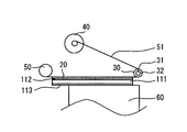
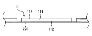
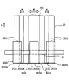
- Sectional drawing of the optical film by 1st embodiment. The whole block diagram which shows the film peeling apparatus by 1st embodiment.
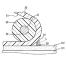
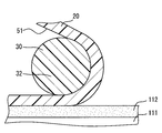
- Sectional drawing which expands and shows a mode that self-discharge is carried out in the location to peel by 1st embodiment.
- Sectional drawing of the optical film by 2nd embodiment. The whole block diagram which shows the film peeling apparatus by 2nd embodiment.
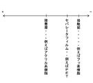
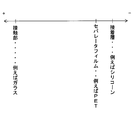
- Explanatory drawing which shows the sticking process of the film peeling apparatus by 2nd embodiment Explanatory drawing which shows the electrification tendency of each element by 2nd embodiment.
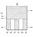
- Sectional drawing which shows the film peeling apparatus by 3rd embodiment The perspective view which shows the film peeling apparatus by 3rd embodiment.
- Explanatory drawing which shows the electrification tendency of each element by the modification 1 of 1st, 2nd and 3rd embodiment Explanatory drawing which shows the electrification tendency of each element by the modification 2 of 1st and 3rd embodiment.
- Sectional drawing which shows the film peeling apparatus by the modification 4 of 3rd embodiment Sectional drawing which shows the film peeling apparatus by the modification 5 of 2nd embodiment.
- Sectional drawing which shows the film peeling apparatus by the modifications 6, 7, and 8 of 3rd embodiment Sectional drawing which shows the film peeling apparatus by the modifications 9 and 10 of 3rd embodiment.
- a display panel 10 as an object to be bonded targeted by the first embodiment of the present disclosure is a liquid crystal panel having a liquid crystal cell layer 120, and the liquid crystal cell layer 120 is sandwiched therebetween.
- a pair of polarizing films 11 are stuck together.
- the liquid crystal cell layer 120 is composed of a pair of electrode substrates 12 and a liquid crystal material sealed between the pair of electrode substrates 12, and by applying electricity, the alignment of the molecules of the liquid crystal material aligns the light.
- a transparent electrode film (not shown) made of ITO (indium tin oxide) or the like is formed on inner surfaces of the pair of electrode substrates 12 facing each other so as to correspond to positions where electricity is applied.
- the polarizing film 11 is a multilayer structure film including a polarizing layer 111 that is a base layer, a surface protective layer 113, an adhesive layer 112, and a separator film 20.
- the polarizing layer 111 as an optical layer that transmits light of a specific wavelength is made of an insulating material such as PVA, for example.
- the surface protective layer 113 that protects the polarizing layer 111 from the outside is made of a transparent material such as glass or resin, for example, and prevents the polarizing layer 111 from being damaged.
- the adhesive layer 112 for attaching the polarizing layer 111 to the liquid crystal cell layer 120 is made of an adhesive such as an acrylic resin, for example.
- the separator film 20 that protects the adhesive layer 112 before being attached to the liquid crystal cell layer 120 is made of an insulating material such as PET (polyethylene terephthalate).
- the film peeling apparatus As shown in FIGS. 3 and 4, the film peeling apparatus according to the first embodiment is provided with a tape body 50, a drawing tape 51, a guide portion 30, in order to peel the separator film 20 from the adhesive layer 112 of the polarizing film 11.
- the take-up reel 40 and the film support table 60 are provided.
- the tape body 50 is an assembly in which a thin strip-shaped drawing tape 51 is wound, and the drawing tape 51 can be drawn by rotation.
- the drawing tape 51 is drawn from the tape body 50 in a drawing direction A that substantially coincides with the horizontal direction.
- the drawing tape 51 has an adhesive surface that can be attached to the separator film 20 of the polarizing film 11.
- the drawing tape 51 is formed in a dimension narrower than the guide portion 30 described later in detail in the width direction substantially perpendicular to the drawing direction A. As a result, the drawing tape 51 is attached to both edges in the width direction of the separator film 20, but is not attached to the intermediate portion of the separator film 20 in the width direction. That is, the drawing tape 51 is wound around the tape body 50 so as to be attached to the separator film 20 in two rows at intervals in the width direction of the separator film 20.
- the guide portion 30 that bends the drawing tape 51 and guides it in the pulling direction B is formed in a columnar shape substantially perpendicular to the drawing direction A.
- the position of the guide portion 30 is fixed to a location where the separator film 20 is peeled from the adhesive layer 112 among the locations ahead of the drawing direction A.
- the guide part 30 has a core member 31 and a contact part 32.
- the core member 31 is made of a metal such as a steel material, for example, and is provided in the radial center portion of the guide portion 30.
- the contact part 32 is made of an insulating material such as a fluororesin, for example, and forms the surface of the guide part 30 by covering the outer peripheral side of the core member 31 having higher rigidity than itself.
- the contact portion 32 applies tension to the drawing tape 51 by bringing the cylindrical outer peripheral surface into contact with the surface opposite to the bonding surface of the drawing tape 51.
- the drawing tape 51 is pulled along the guide portion 30 together with the separator film 20 so that the drawing tape 51 is bent toward the pulling direction B that forms an acute angle on the upper side with respect to the drawing direction A.
- the bending angle at which the separator film 20 is bent in the tensile direction B is set to an acute angle.
- the charging tendency of the contact portion 32 (for example, fluororesin) is charged on the separator film 20 (for example, PET) on the charging train representing the ease of inducing positive or negative charges.
- the adhesive layer 112 (for example, acrylic resin or the like) is located on the opposite side to the charging tendency with the tendency interposed therebetween. That is, the charging tendency of the separator film 20 shows a property between the charging tendency of the contact portion 32 and the charging tendency of the adhesive layer 112.
- the contact portion 32 is more likely to induce a negative charge than the separator film 20 and the adhesive layer 112 on the charged row, and the separator film 20 is more negative than the adhesive layer 112 on the charged row. It is easy to induce the charge.
- the take-up reel 40 that winds the drawing tape 51 is formed in a columnar shape that is substantially perpendicular to the pulling direction B, and is rotatably provided obliquely above the guide portion 30. Yes.
- the winding reel 40 winds and collects the drawing tape 51 while being pulled in the pulling direction B together with the attached separator film 20 by rotation.
- the take-up reel 40 is configured to be taken up by an electric motor (not shown), and the take-up reel 51 is drawn out from the tape body 50 by the take-up reel 40 being taken up by the electric motor. .
- the film support table 60 that supports the polarizing film 11 is made of a metal such as aluminum, for example, and is provided below the tape body 50 and the guide part 30.
- the film support table 60 can be displaced in a sliding direction C along the drawing direction A.
- the film support table 60 is provided with an adsorber (not shown) that vacuum-adsorbs the polarizing film 11.
- the polarizing film 11 can be displaced in the sliding direction C together with the film support table 60 by being fixed on the film support table 60 with the separator film 20 side facing upward by the vacuum suction function of the suction device.
- the polarizing film 11 can be separated from the film support table 60 by releasing the suction function of the suction unit.
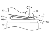
- the film peeling apparatus includes a cell adsorption table 70, in addition to the film support table 60, in order to attach the adhesive layer 112 peeled from the separator film 20 to the liquid crystal cell layer 120. , A sticking roller 80 is provided.
- the cell suction table 70 is made of metal and used with its position fixed.
- the cell suction table 70 is provided with a suction unit (not shown) that vacuum-sucks the display panel 10.
- the display panel 10 is fixed on the cell suction table 70 with one electrode substrate 12 facing upward by the vacuum suction function of the suction unit.
- the sticking roller 80 is formed of a metal in a columnar shape and is provided above the cell suction table 70.
- the affixing roller 80 is provided so as to be displaceable and rotatable in a movable direction D that substantially coincides with the horizontal direction.
- the sticking roller 80 is pressed from above against the surface protective layer 113 of the polarizing film 11 with the adhesive layer 112 facing downward. By this pressing, the adhesive layer 112 is pressed against the upper electrode substrate 12 of the display panel 10 on the cell suction table 70, and in this state, the adhesive roller 112 is displaced in the sliding direction D while rotating the application roller 80. The pasting of the layers 112 and 12 is realized.
- the film support table 60 for attaching the adhesive layer 112 to the electrode substrate 12 is disposed above the cell adsorption table 70 so that the polarizing film 11 that is turned upside down can be vacuum-sucked from the surface protective layer 113 side. become.
- the preparation process shown in FIG. 3 is performed. Specifically, one polarizing film 11 with the separator film 20 side facing upward is fixed on the film support table 60 by an adsorber (not shown). At the same time, the tape body 50 is movably set, and the drawing tape 51 drawn out from the tape body 50 is wound around the take-up reel 40 via the guide portion 30. Here, the take-up reel 40 is movably set. An adhesive layer (not shown) is formed on one surface of the drawing tape 51. Under the above-described state, the separator film 20 of the polarizing film 11 is pressed against the adhesive layer of the drawing tape 51 between the tape body 50 and the guide portion 30, and is adhered to the adhesive layer.
- the peeling step shown in FIG. 4 is performed. Specifically, by rotating the take-up reel 40 with an electric motor, the tape body 50 is driven to rotate, and the drawing tape 51 is drawn in the drawing direction A. At this time, the drawing tape 51 receives a force from the contact portion 32 of the guide portion 30 and is bent by the guide function of the guide portion 30 while being kept in tension, and wound on the take-up reel 40. It is pulled in the pulling direction B. At the same time, the film support table 60 is displaced in the slide direction C. Thus, the separator film that maintains the sticking state with the drawing tape 51 in combination with the drawing tape 51 being pulled in the pulling direction B and the displacement of the film support table 60 in the sliding direction C. 20 is peeled off from the adhesive layer 112 of the polarizing film 11 at the place of contact with the contact portion 32. The peeled separator film 20 is pulled in the pulling direction B together with the drawing tape 51 and wound on the take-up reel 40.
- the film support table 60 is conveyed to the pasting process side shown in FIG. Specifically, in the attaching step, the display panel 10 with one electrode substrate 12 facing upward is fixed to the cell adsorption table 70 by an adsorber (not shown). Under such a state, the polarizing film 11 is fixed to the film support table 60 by an adsorber (not shown), and the film support table 60 is turned upside down by a transporter (not shown). The film support table 60 turned upside down is conveyed so as to face the electrode substrate 12 of the display panel 10 fixed to the suction table 70.
- the application roller 80 is pressed against the polarizing film 11 protruding from the side surface of the film support table 60, and the end of the adhesive layer 112 is pressed against the upper electrode substrate 12.
- the rotating portion of the sticking roller 80 has a cylindrical shape, and the length of the cylindrical shape (that is, the length in the direction perpendicular to the paper surface of FIG. 5) is substantially the same as the entire width direction of the polarizing film 11. It is set to the same length.
- the fixing of the polarizing film 11 to the film support table 60 by the adsorber is released, and the film support table 60 is returned to the peeling process side.
- the remaining part of the adhesive layer 112 is pressed against the upper electrode substrate 12 by rotating the sticking roller 80 pressed against the polarizing film 11 in the movable direction D while rotating.
- the polarizing film 11 is attached to the adhesive layer 112 of the liquid crystal cell layer 120 without air mixing.
- the negative charge Q1 is present near the surface of the separator film 20 and the surface of the adhesive layer 112 due to the above-described charging tendency relationship.
- a positive charge Q2 is respectively induced in.
- the contact portion 32 made of fluororesin is not in the guide portion 30, that is, if the core member 31 made of metal is in direct contact with the separator film 20, the negative charge Q1 is released to the core member 31. It is not held near the surface of the separator film 20.
- the positive charge Q2 of the adhesive layer 112 is difficult to escape to the polarizing layer 111 made of an insulating material, it remains held near the surface of the adhesive layer 112. As a result, when the adhesive layer 112 having a large charge amount is attached to the electrode substrate 12 of the display panel 10, the electrode film of the liquid crystal cell layer 120 may be damaged, or foreign matter may be mixed between the layers 112 and 12. Occurs.
- the contact portion 32 is made of, for example, a fluororesin or the like, and therefore, it becomes easier to induce the negative charge Q1 than the separator film 20 and the adhesive layer 112 due to the above-described charging tendency relationship. (See FIG. 6). That is, the negative charge Q1 is less likely to escape from the separator film 20 at the contact portion 32 where charge induction having a polarity opposite to that of the adhesive layer 112 is likely to occur, and is held near the surface of the separator film 20. Therefore, a self-discharge L is generated between the negative charge Q1 held near the surface of the separator film 20 and the positive charge Q2 held near the surface of the adhesive layer 112, which is difficult to escape from the polarizing layer 111. It will be.
- the charging tendency of the separator film 20 is a property between the charging tendency of the guide portion 30 and the charging tendency of the adhesive layer 112. Therefore, the surface of the guide portion 30 that is in contact with the separator film 20 exhibits a property opposite to the charging tendency of the adhesive layer 112 across the charging tendency of the separator film 20 on the charging train. According to this, the charge Q1 having a polarity opposite to that of the adhesive layer 112 is more easily induced than the separator film 20, and the charge Q1 induced in the separator film 20 due to the peeling charge at the time of peeling is difficult to escape.
- the induced charge Q1 to be held by the separator film 20 can generate a self-discharge L between the charge Q2 having the opposite polarity induced in the adhesive layer 112 by the peeling charge. Therefore, even if the separator film 20 is peeled off from the adhesive layer 112, the induced charge Q2 can be extinguished without being held in the adhesive layer 112.
- the self-discharge L progresses over the entire separator film 20 while the separator film 20 is peeled off from the adhesive layer 112 by the guide portion 30. According to this, it is possible to eliminate the induced charge Q ⁇ b> 2 without being held on the entire surface of the adhesive layer 112 by peeling the entire separator film 20.
- the separator film 20 of the first embodiment is pulled in the pulling direction B together with the drawing tape 51 attached thereto.
- the separator film 20 can be easily peeled from the adhesive layer 112 by the guide portion 30 by the drawing tape 51 to which tension is applied. According to this, it is possible to enhance the effect of improving the productivity of the display panel 10 as well as the effect of eliminating the induced charge Q2 without being held in the adhesive layer 112.
- the guide part 30 of the first embodiment has a core member 31 that is higher in rigidity than the contact part 32 that contacts the drawing tape 51. According to this, since the guide part 30 can endure the reaction force of the tension
- the charging tendency of the contact portion 32 that covers the outer peripheral side of the core member 31 and contacts the drawing tape 51 is the charging tendency of the adhesive layer 112 across the charging tendency of the separator film 20 on the charging train. The opposite side property is shown.
- the induced charge Q ⁇ b> 1 is not easily released to the guide portion 30 regardless of the constituent members of the core member 31, and the self-discharge L can be generated between the separator film 20 and the adhesive layer 112. From the above, it is possible to increase the sustainability of the effect of eliminating the induced charge Q2 without holding it in the adhesive layer 112.
- the drawing tape 51 of the first embodiment is formed to have a narrower dimension than the guide portion 30 in the width direction. Accordingly, the area where the contact portion 32 and the separator film 20 are brought into contact with each other can be increased while the ease of peeling of the separator film 20 by the drawing tape 51 is increased, and the self-discharge L can be generated between the elements 32 and 20. Therefore, it is possible to increase the certainty of the effect of eliminating the induced charge Q2 without holding it in the adhesive layer 112.
- the separator film 20 of the first embodiment can be easily peeled from the adhesive layer 112 by being bent in the tensile direction B by the guide portion 30.
- the angle at which the separator film 20 is bent in the tensile direction B is set to an acute angle by the guide portion 30, so that tension is appropriately applied to the separator film 20 and the separator film 20 is bonded to the adhesive layer 112. Can be efficiently peeled off. According to these, it is possible to enhance the effect of improving the productivity of the display panel 10 as well as the effect of eliminating the induced charge Q2 without being held in the adhesive layer 112.
- FIGS. 8 to 12 The second embodiment of the present disclosure shown in FIGS. 8 to 12 is a modification of the first embodiment.
- a tape-like separator film 220 made of an insulating material such as PET is shared by a plurality of polarizing films 11.
- each polarizing film 11 has a multilayer structure in which an adhesive layer 112, a polarizing layer 111 and a surface protective layer 113 are laminated on a common separator film 220.
- the film peeling apparatus has a film support table 260, a take-up reel 240, and an adsorption device for peeling the separator film 220 from the adhesive layer 112 of each polarizing film 11.
- the film support table 260 for supporting the polarizing film 11 has a main body part 261 and a guide part 263.
- the main body 261 is made of a metal such as aluminum, for example, and the separator film 220 is introduced in the introduction direction E substantially in the horizontal direction above the main body 261.
- the main body 261 sequentially supports each polarizing film 11 introduced by the common separator film 220.
- the entire guide portion 263 including the surface thereof is made of an insulating material such as a fluororesin, and is fixed to the main body portion 261 having a higher rigidity than that of the guide portion 263 from below.
- the guide portion 263 is provided at a front corner portion 262 in the introduction direction E of the film support table 260 as a location where the separator film 220 is peeled from the adhesive layer 112.
- the separator film 220 is bent while being guided along the guide portion 263, thereby being bent in a tensile direction B that is perpendicular to the introduction direction E. That is, the bending angle at which the separator film 220 is bent in the tensile direction B is set to a right angle.
- the guide part 263 that bends the separator film 220 has a right-angled shape
- the guide film 263 may be chamfered, for example, in an arc shape so as not to damage the separator film 220.
- the charging tendency of the guide portion 263 (for example, a fluororesin) on the charge train is determined by sandwiching the charging tendency of the separator film 220 (for example, PET) on the adhesive layer 112 ( For example, it is located on the opposite side of the charging tendency of acrylic resin. That is, the charging tendency of the separator film 220 indicates a property between the charging tendency of the guide portion 263 and the charging tendency of the adhesive layer 112.
- the guide portion 263 is more likely to induce a negative charge than the separator film 220 and the adhesive layer 112 on the charged row, and the separator film 220 is more negative than the adhesive layer 112 on the charged row. It is easy to induce the charge.
- the take-up reel 240 that winds up the separator film 220 is formed in a columnar shape substantially perpendicular to the pulling direction B, and is rotatably provided below the guide portion 263. .
- the take-up reel 240 winds and collects the separator film 220 while pulling the separator film 220 in the pull direction B by rotation.
- the suction pick 290 is provided above the film support table 260 and can be displaced in a movable direction F along the introduction direction E.
- the suction pick 290 is provided with a suction device 291 that vacuum-sucks each polarizing film 11 from the surface protective layer 113 side.
- the polarizing film 11 reaches the guide portion 263 as shown in FIG. 9 by this vacuum suction function, the polarizing film 11 is held by the suction device 291 pressed against the surface protective layer 113 from above, and moves together with the suction device 291 in the movable direction F. Displaceable.
- the film peeling apparatus according to the second embodiment is the same as the first embodiment in addition to the above-described suction pick 290 in order to stick the adhesive layer 112 peeled from the separator film 220 to the electrode substrate 12.
- a cell suction table 70 and a sticking roller 80 having the same configuration are provided.
- the suction pick 290 for attaching the adhesive layer 112 to the electrode substrate 12 is disposed above the cell suction table 70 so that the polarizing film 11 can be vacuum-sucked from the surface protective layer 113 side.
- the tape-like separator film 220 supported by the film support table 260 is wound around the take-up reel 240 via the guide portion 263. .
- the take-up reel 240 is rotated by an electric motor (not shown) to introduce the plurality of polarizing films 11 in the introduction direction E.
- the plurality of polarizing films 11 are bonded to the separator film 220 having a continuous length through the adhesive layer 112 so as to be spaced apart from each other.
- the polarizing film 11 is not bonded to the region of the separator film 220 over a predetermined length, and this non-bonded region is bent by the guide function of the guide portion 263 and wound around the take-up reel 240. Thus, it is pulled in the pulling direction B.
- each polarizing film 111 reaches the guide portion 263, the surface protective layer 113 is vacuum-sucked by the suction pick 290 and is displaced in the movable direction F together with the suction pick 290.
- the separator film 220 is pulled in the pulling direction B, and the polarizing film 11 is displaced in the movable direction F by the suction pick 290, so that the separator film 220 is connected to the guide portion 263. It will peel from the adhesive layer 112 of each polarizing film 11 in a contact location.
- the separated separator film 220 is taken up by the take-up reel 240.
- the polarizing film 11 from which the separator film 220 has been peeled is conveyed to the sticking process side shown in FIG. 11 while being adsorbed by the adsorption pick 290.
- the display panel 10 with one electrode substrate 12 of the liquid crystal cell layer 120 facing upward is fixed to the surface of the cell adsorption table 70 by an adsorber (not shown).
- the sticking roller 80 is pressed against the polarizing film 11 that has been sucked by the suction pick 290, and the end of the adhesive layer 112 is pressed against the upper electrode substrate 12.
- the rotating portion of the sticking roller 80 has a cylindrical shape, and the length of the cylindrical shape (that is, the length in the direction perpendicular to the paper surface of FIG. 11) is substantially the same as the entire width direction of the polarizing film 11. It is set to the same length.
- the suction by the suction pick 290 is canceled and the suction pick 290 is returned to the peeling process side.
- the remaining part of the adhesive layer 112 is pressed against the upper electrode substrate 12 by rotating the sticking roller 80 pressed against the polarizing film 11 in the movable direction D while rotating.
- the polarizing film 11 is attached to the adhesive layer 112 of the liquid crystal cell layer 120 without air mixing.
- the charging tendency of the separator film 220 is a property between the charging tendency of the guide portion 263 and the charging tendency of the adhesive layer 112 as shown in FIG. Therefore, the surface of the guide portion 263 that is in contact with the separator film 220 exhibits a property opposite to the charging tendency of the adhesive layer 112 across the charging tendency of the separator film 220 on the charging train. Therefore, the self-discharge L is generated between the separator film 220 and the adhesive layer 112 by the same principle as in the first embodiment, and the induced charge Q2 can be extinguished without being held in the adhesive layer 112.
- the self-discharge L progresses over the entire separator film 220 while the separator film 220 is peeled off from the adhesive layer 112 by the guide portion 263. According to this, it is possible to eliminate the induced charge Q2 without holding the entire surface of the adhesive layer 112 by peeling the entire separator film 220.
- the guide part 263 of 2nd embodiment is provided using the corner
- the main body portion 261 of the film support table 260 has higher rigidity than the guide portion 263. According to this, since the main-body part 261 can endure the reaction force of the tension
- FIGS. 13 and 14 The third embodiment of the present disclosure shown in FIGS. 13 and 14 is a modification of the first embodiment.
- the drawing tape 3051 of the third embodiment is arranged in a form in which three are arranged in the width direction W substantially perpendicular to the drawing direction A.
- the configuration of each drawing tape 3051 is substantially the same as that of the drawing tape 51 of the first embodiment, except for the dimension in the width direction W described in detail later.
- the guide portion 3030 of the third embodiment is composed of three contact portions 3032 and a core member 31 common to the contact portions 3032.
- the contact portions 3032 are spaced apart from each other in the width direction W of the tape 3051 so as to be in contact with each other so as to be able to come into contact with the drawing tape 3051 provided individually.
- each drawing tape 3051 is disposed so as to avoid between the contact portions 3032, that is, to expose the separator film 20 to the space portion 3033 between the contact portions 3032.
- each drawing tape 3051 is formed in a narrower dimension than the corresponding contact portion 3032 in each width direction W. Due to these arrangements and dimensions, each contact portion 3032 comes into contact with the separator film 20 via the corresponding drawing tape 3051 at the center portion in the respective width direction W, while on both edge sides in each width direction W, Directly contacts with the separator film 20.
- each contact portion 3032 is substantially the same as the contact portion 32 of the first embodiment except for the points described above. Therefore, on the charging train, the charging tendency of each contact portion 3032 (for example, a fluororesin) is charged by the adhesive layer 112 (for example, an acrylic resin) with the charging tendency of the separator film 20 (for example, PET) interposed therebetween. Located on the opposite side of the trend. That is, the charging tendency of the separator film 20 indicates a property between the charging tendency of each contact portion 3032 and the charging tendency of the adhesive layer 112. Particularly in the third embodiment, each contact portion 3032 is more likely to induce a negative charge than the separator film 20 and the adhesive layer 112 on the charged row.
- the adhesive layer 112 for example, an acrylic resin
- the separator film 20 for example, PET
- each contact portion 3032 forming the surface of the guide portion 3030 applies tension to the corresponding drawing tape 3051 and guides the separator film 20 together with the corresponding tape 3051 in the pulling direction B (not shown). Bend. At this time, both edge portions 3020a and 3020b of the separator film 20 in the width direction W of each drawing tape 3051 are individually in contact with the pair of edge-side contact portions 3032a and 3032b among the plurality of contact portions 3032. Bend. In addition, in the third embodiment, the central portion 3020c of the separator film 20 in the width direction W of each drawing tape 3051 is in contact with the central contact portion 3032c between the edge side contact portions 3032a and 3032b among the plurality of contact portions 3032. Bend.
- the surface of each contact portion 3032 that comes into contact with the extraction tape 3051 and the separator film 20 in the guide portion 3030 has the charging tendency of the separator film 20 on the charging column.
- the property opposite to the charging tendency is exhibited. That is, the charging tendency of the separator film 20 is a property between the charging tendency of the guide portion 3030 and the charging tendency of the adhesive layer 112. According to this, the induced charge Q ⁇ b> 1 is not easily released to the guide portion 3030 regardless of the constituent members of the core member 31, and the self-discharge L can be generated between the separator film 20 and the adhesive layer 112.
- both edge portions 3020a and 3020b of the separator film 20 in the width direction W of the drawing tape 3051 are individually connected to the pair of edge side contact portions 3032a and 3032 among the plurality of contact portions 3032, respectively. Contact. According to this, the separator film 20 can be reliably peeled between the edge portions 3020a and 3020b with respect to the adhesive layer 112, and the self-discharge L at that time can be surely generated. Therefore, it is possible to increase the certainty of the effect of eliminating the induced charge Q2 without holding it in the adhesive layer 112.
- the drawing tape 3051 disposed so as to avoid the space between the contact portions 3032 can be brought into contact with the contact portions 3032 with certainty to provide the tension necessary for peeling. According to this, the self-discharge L at the time of peeling can be produced reliably while avoiding the peeling failure between the adhesive layer 112 and the separator film 20. Therefore, it is possible to increase the certainty of the effect of eliminating the induced charge Q2 without holding it in the adhesive layer 112.
- a plurality of drawing tapes 3051 provided corresponding to each contact portion 3032 are arranged not only between the contact portions 3032 but also in the width direction W.
- the contact portion 3032 is formed with a narrower dimension. According to this, any of the contact portions 3032 is brought into contact with the separator film 20 to make it difficult for the induced charge to escape to the guide portion 3030, so that the self-discharge L at the time of peeling can be surely generated. Therefore, it is possible to increase the certainty of the effect of eliminating the induced charge Q2 without holding it in the adhesive layer 112.
- polypropylene Cellophane polyvinyl chloride, silicone rubber, ebonite and the like may be employed as the forming material of the contact portions 32, 3032 and the guide portion 263. Since these polypropylene, cellophane, polyvinyl chloride, silicone rubber, and ebonite are more likely to induce negative charges than PET and acrylic resins, as in the case of fluororesins, the same effects as in any of the embodiments can be obtained. .
- the contact portions 32 and 3032 made of, for example, glass, the separator film 20 made of, for example, PET, and the adhesive layer 112 made of, for example, a silicone adhesive are employed. Also good. According to the second modification, as shown in FIG. 16, the contact portions 32 and 3032 are more likely to induce a positive charge than the separator film 20 and the adhesive layer 112 on the charged row, and the separator film on the charged row. 20 is easier to induce a positive charge than the adhesive layer 112. This indicates that the charging tendency of the contact portions 32 and 3032 is located on the opposite side of the charging tendency of the adhesive layer 112 across the charging tendency of the separator film 20. That is, the charging tendency of the separator film 20 indicates a property between the charging tendency of the contact portions 32 and 3032 and the charging tendency of the adhesive layer 112.
- a positive charge Q2 is induced near the surface of the separator film 20, and a negative charge Q1 is induced near the surface of the adhesive layer 112.
- the contact portions 32 and 3032 are easier to induce a positive charge Q2 than the separator film 20 and the adhesive layer 112. That is, the positive charge Q2 is difficult to escape from the separator film 20 at the contact portions 32 and 3032 where charge induction having a polarity opposite to that of the adhesive layer 112 is likely to occur, and is held near the surface of the separator film 20. Accordingly, a self-discharge L is generated between the positive charge Q2 held near the surface of the separator film 20 and the negative charge Q1 held near the surface of the adhesive layer 112, which is difficult to escape from the polarizing layer 111. It will be.
- the guide portions 30 and 3030 may be rotatable. According to the third modification, friction between the drawing tapes 51 and 3051 and the separator film 20 and the contact portions 32 and 3032 is reduced. As a result, the contact portions 32 and 3032 are less likely to be worn, and thus it is possible to prevent the negative charge Q1 from escaping from the separator film 20 to the core member 31 made of metal for a long time.
- the guide portions 30 and 3030 may be configured only from the contact portions 32 and 3032 without providing the core member 31.
- support structures 3034 that support the contact portions 3032 are provided on both sides of each contact portion 3032.
- the space part 3233 is opened, and the some guide part 263 spaced apart from each other. May be supported by the main body 261.
- the drawing tape 3051 may be arranged so as to protrude between the contact portions 3032. Further, in Modification 10 of the third embodiment, as shown in FIG. 21, the drawing tape 3051 (in the figure, one in the middle) is formed in a dimension wider than the contact portion 3032 in the width direction W. May be. In addition, about the modification 10, it can apply also to 1st embodiment by replacing the drawing tape 3051 and the contact part 3032 with the drawing tape 51 and the contact part 32, respectively.
- the folding angle at which the separator film 20 is folded in the tensile direction B may be set to a right angle or an obtuse angle.
- the polarizing film 11 provided with the polarizing layer 111 as a base layer of the multilayered structure film 11, it is not restricted to the polarizing film 11 as the modification 13 of those embodiment.
- it may be a base layer such as a protective film for protecting the surface of the liquid crystal display.
- the display panel 10 is adopted as the bonding target.
- the modification 14 of the embodiments is not limited to this, for example, a panel that requires surface protection, an electronic device, and the like.
- An electronic panel provided with components may be used.
Landscapes
- Laminated Bodies (AREA)
- Folding Of Thin Sheet-Like Materials, Special Discharging Devices, And Others (AREA)
- Lining Or Joining Of Plastics Or The Like (AREA)
Abstract
多層構造フィルム(11)において接着層(112)を保護するセパレータフィルム(20)を剥離するフィルム剥離装置は、ガイド部(30、263、3030)を備える。ガイド部(30、263、3030)は、セパレータフィルム(20)に接触しながらセパレータフィルム(20)をガイドする。正または負の電荷の誘導しやすさを表す帯電列上において、セパレータフィルム(20)の帯電傾向は、ガイド部(30、263、3030)の帯電傾向と接着層(112)の帯電傾向との間の性質を示す。
Description
本開示は、2012年12月24日に出願された日本出願番号2012-280405号と2013年8月28日に出願された日本出願番号2013-177178号に基づくもので、ここにその記載内容を援用する。
本開示は、多層構造フィルムにおいて接着層を保護するセパレータフィルムを剥離するフィルム剥離装置及び方法に関する。
従来、液晶ディスプレイなどの表示パネルには、視野角を広げるために、光の位相差の変化を補償する位相差フィルムや、光の位相を整える偏光フィルムなどの光学フィルムが貼付けられる。一般に光学フィルムは、その光学機能を発揮するための光学層の他に、表示パネルに貼付けるための接着層や、接着層を貼付け前まで保護しておくためのセパレータフィルムが設けられることで、多層構造を呈している。こうした多層構造のフィルムにおいてセパレータフィルムを剥離した接着層を、表示パネルに貼付けることにより、光学フィルムとしての光学機能を発揮可能となる。そこで、特許文献1には、セパレータフィルムを剥離するフィルム剥離装置が提案されている。
さて、特許文献1に開示の如きフィルム剥離装置を用いてセパレータフィルムを剥離する際には、接着層とセパレータフィルムとの間で剥離帯電が生じる可能性がある。
ここで剥離帯電とは、互いに密着している部材同士を剥離する際に、一方の部材の表面付近と他方の部材の表面付近とにそれぞれ逆極性の電荷、即ち正電荷と負電荷とが誘導されることで、それら各部材が帯電する現象である。したがって、光学フィルムの接着層からセパレータフィルムを剥離した際には、剥離帯電による誘導電荷が接着層に保持されたままとなる。そのため、接着層を介して光学フィルムを表示パネルに貼付けてしまうと、接着層と表示パネルとの間で放電が生じる。その結果、表示パネルの電極などを損傷させる可能性や、帯電によって吸着される空気中の異物が表示パネルの接着層との間に混入して製品不良となる可能性につながる。
そこで、剥離帯電を防止するために特許文献1に開示のフィルム剥離装置では、イオナイザなどのイオン送風機が設けられている。かかる開示装置によれば、イオン送風機によってイオン化したエアを、接着層とセパレータフィルムとの間に送ることで、光学フィルムの接着層に保持される電荷を除去することが可能となる。
しかし、特許文献1に開示のフィルム剥離装置の場合、イオン化エアの届かなかった箇所は、剥離帯電による誘導電荷を保持することになる。また、イオン化エアを送ることにより、空気中の異物が接着層付近に送られるため、かかる異物が接着層に吸着されやすくなる。
本開示の目的は、光学フィルムなどの多層構造フィルムの接着層からセパレータフィルムを剥離した際に、誘導電荷を当該接着層に保持させることなく消滅させるフィルム剥離装置及び方法を、提供することにある。
本開示にかかる第一例によれば、母体層と、母体層に接着層を介して貼付けられたセパレータフィルムとを包含する多層構造フィルムにおいて、接着層を保護するセパレータフィルムを剥離するフィルム剥離装置は、セパレータフィルムに接触しながらセパレータフィルムをガイドして、セパレータフィルムを接着層から剥離するガイド部を備える。正または負の電荷の誘導しやすさを表す帯電列上において、セパレータフィルムの帯電傾向は、ガイド部の帯電傾向と接着層の帯電傾向との間の性質を示す。
剥離帯電に関しては、部材間における相対的な帯電のしやすさ、すなわち各部材における正または負の電荷の誘導しやすさを表した帯電列が知られており、当該帯電列上の相対位置は、各部材の帯電傾向を示すことになる。
第一例のフィルム剥離装置によると、セパレータフィルムの帯電傾向を、ガイド部の帯電傾向と接着層の帯電傾向との間の性質としている。これによれば、接着層とは逆極性の電荷がセパレータフィルムよりも誘導されやすいガイド部には、剥離時の剥離帯電によりセパレータフィルムに誘導された電荷が逃げにくくなる。その結果、セパレータフィルムに保持されることになる誘導電荷は、剥離帯電により接着層に誘導された逆極性の電荷との間で、放電(以下、自己放電と呼ぶ)を生じ得る。したがって、セパレータフィルムを接着層から剥離しても、誘導電荷を当該接着層に保持させることなく消滅させることが可能となる。
本開示にかかる第二例によれば、母体層と、母体層に接着層を介して貼付けられたセパレータフィルムとを包含する多層構造フィルムにおいて、接着層を保護するセパレータフィルムを剥離するフィルム剥離装置は、セパレータフィルムに接触しながらセパレータフィルムをガイドして、セパレータフィルムを接着層から剥離するガイド部を備える。ガイド部のうちセパレータフィルムと接触する表面は、正または負の電荷の誘導しやすさを表す帯電列上において、セパレータフィルムの帯電傾向を挟んで接着層の帯電傾向とは反対側の性質を示す材料により構成されている。
第二例のフィルム剥離装置によると、ガイド部のうちセパレータフィルムと接触する表面は、セパレータフィルムの帯電傾向を挟んで接着層の帯電傾向とは反対側の性質を示すことになる。これによれば、上述した第一例のフィルム剥離装置と同様な作用効果を得ることができる。
本開示にかかる第三例によれば、母体層と、母体層に接着層を介して貼付けられたセパレータフィルムとを包含する多層構造フィルムにおいて、接着層を保護するセパレータフィルムを剥離するフィルム剥離方法は、セパレータフィルムを接着層から剥離させる箇所に設けたガイド部に、セパレータフィルムを接触させながら、セパレータフィルムをガイドして、セパレータフィルムを剥離する剥離工程を含み、正または負の電荷の誘導しやすさを表す帯電列上において、セパレータフィルムの帯電傾向を、ガイド部の帯電傾向と接着層の帯電傾向との間の性質を示す。
第三例のフィルム剥離方法によると、セパレータフィルムの帯電傾向を、ガイド部の帯電傾向と接着層の帯電傾向との間の性質としているので、上述した第一例のフィルム剥離装置と同様な作用効果を得ることができる。
本開示にかかる第四例によれば、母体層と、母体層に接着層を介して貼付けられたセパレータフィルムとを包含する多層構造フィルムにおいて、接着層を保護するセパレータフィルムを剥離するフィルム剥離方法であって、セパレータフィルムを接着層から剥離させる箇所に設けたガイド部に、セパレータフィルムを接触させながら、セパレータフィルムをガイドして、セパレータフィルムを剥離する剥離工程を含み、ガイド部のうちセパレータフィルムと接触する表面を、正または負の電荷の誘導しやすさを表す帯電列上において、セパレータフィルムの帯電傾向を挟んで接着層の帯電傾向とは反対側の性質を示す材料により構成する。
第四例のフィルム剥離方法によると、ガイド部のうちセパレータフィルムと接触する表面は、セパレータフィルムの帯電傾向を挟んで接着層の帯電傾向とは反対側の性質を示すことになる。これによれば、上述した第一例のフィルム剥離装置と同様な作用効果を得ることができる。
以下、本開示の複数の実施形態を図面に基づいて説明する。尚、各実施形態において対応する構成要素には同一の符号を付すことにより、重複する説明を省略する場合がある。各実施形態において構成の一部分のみを変更している場合、当該構成の他の部分においては、先行して説明した他の実施形態の構成を適用することができる。また、各実施形態の説明において明示している構成の組み合わせだけでなく、特に組み合わせに支障が生じなければ、明示していなくとも複数の実施形態の構成同士を部分的に組み合わせることが可能である。
(第一実施形態)
図1に示されるように、本開示の第一実施形態が対象とする接着対象体としての表示パネル10は、液晶セル層120を有する液晶パネルであって、この液晶セル層120を間に挟むようにして一対の偏光フィルム11が貼付けられている。ここで液晶セル層120は、一対の電極基板12とこの一対の電極基板12の間に封入された液晶材料からなり、電気を印加することにより液晶材料の分子の配向が整列することで光の入出を調整するシャッター機能を有する。一対の電極基板12の互いに対向する内側面には、電気を印加する位置に対応するように、図示しない例えばITO(インジウムスズ酸化物)などから構成された透明電極膜が形成されている。
図1に示されるように、本開示の第一実施形態が対象とする接着対象体としての表示パネル10は、液晶セル層120を有する液晶パネルであって、この液晶セル層120を間に挟むようにして一対の偏光フィルム11が貼付けられている。ここで液晶セル層120は、一対の電極基板12とこの一対の電極基板12の間に封入された液晶材料からなり、電気を印加することにより液晶材料の分子の配向が整列することで光の入出を調整するシャッター機能を有する。一対の電極基板12の互いに対向する内側面には、電気を印加する位置に対応するように、図示しない例えばITO(インジウムスズ酸化物)などから構成された透明電極膜が形成されている。
図2に示されるように偏光フィルム11は、母体層である偏光層111と、表面保護層113と、接着層112と、セパレータフィルム20とを包含する多層構造フィルムである。特定の波長の光を透過させる光学層としての偏光層111は、例えばPVAなどの絶縁材からなる。偏光層111を外部から保護する表面保護層113は、例えばガラス乃至は樹脂などの透過性材料からなり、偏光層111の損傷を防止する。液晶セル層120に偏光層111を貼付けるための接着層112は、例えばアクリル系樹脂などの接着剤からなる。接着層112を液晶セル層120に貼付ける前まで保護しておくセパレータフィルム20は、例えばPET(ポリエチレンテレフタレート)などの絶縁材からなる。
次に、第一実施形態において、偏光フィルム11からセパレータフィルム20を剥離して当該フィルム11を表示パネル10に貼付ける際に使用されるフィルム剥離装置の構成を、詳細に説明する。
図3、4に示されるように第一実施形態のフィルム剥離装置は、偏光フィルム11の接着層112からセパレータフィルム20を剥離するために、テープ体50と、引出テープ51と、ガイド部30と、巻取リール40と、フィルム支持テーブル60とを備えている。
テープ体50は、薄肉帯状の引出テープ51が巻かれた集合体であり、回転によって引出テープ51を引出し可能となっている。引出テープ51は、水平方向と略一致した引出方向Aへテープ体50から引出される。引出テープ51は、偏光フィルム11のセパレータフィルム20に貼着可能な接着面を有している。引出テープ51は、引出方向Aに略垂直な幅方向において、後に詳述のガイド部30よりも狭い寸法に形成されている。これにより引出テープ51は、セパレータフィルム20の幅方向の両縁部側にそれぞれ貼着されるが、セパレータフィルム20の幅方向の中間部には貼着されないようになっている。即ち、引出テープ51は、セパレータフィルム20の幅方向において互いに間隔を隔てて2列でセパレータフィルム20に貼付けられるように、テープ体50に巻付けられている。
引出テープ51を折曲げて引張方向Bへと導くガイド部30は、引出方向Aに対して略垂直な円柱状に形成されている。ガイド部30は、引出方向Aの前方箇所のうち、セパレータフィルム20を接着層112から剥離させる箇所に位置固定されている。ガイド部30は、芯部材31と、接触部32とを有している。芯部材31は、例えば鉄鋼材料などの金属からなり、ガイド部30の径方向中央部分に設けられている。接触部32は、例えばフッ素樹脂などの絶縁材からなり、自身よりも剛性の高い芯部材31の外周側を覆うことで、ガイド部30の表面を形成している。接触部32は、円筒面状の外周面を引出テープ51の接着面とは反対側の面に接触させることで、引出テープ51に張力を与える。以上の構成により引出テープ51は、セパレータフィルム20と共に、ガイド部30に沿ってガイドされつつ引張られることで、引出方向Aに対して上側に鋭角をなす引張方向Bへ向かって折曲げられることになる。即ち、セパレータフィルム20を引張方向Bへ折曲げる折曲げ角度は、鋭角に設定されている。
図6に示されるように、正または負の電荷の誘導しやすさを表した帯電列上において、接触部32(例えばフッ素樹脂など)の帯電傾向は、セパレータフィルム20(例えばPETなど)の帯電傾向を挟んで、接着層112(例えばアクリル系樹脂など)の帯電傾向とは反対側に位置している。即ちセパレータフィルム20の帯電傾向は、接触部32の帯電傾向と接着層112の帯電傾向との間の性質を示しているのである。そして特に第一実施形態では、帯電列上において接触部32は、セパレータフィルム20及び接着層112よりも負の電荷を誘導しやすく、また帯電列上においてセパレータフィルム20は、接着層112よりも負の電荷を誘導しやすくなっている。
図3、4に示されるように、引出テープ51を巻取る巻取リール40は、引張方向Bに対して略垂直な円柱状に形成され、ガイド部30の斜め上方に回転可能に設けられている。巻取リール40は、回転によって引出テープ51を、貼着状態のセパレータフィルム20と共に引張方向Bへ引張りながら、巻取り回収する。ここで巻取リール40は、電動モータ(図示しない)により巻取られるように構成されており、巻取リール40が電動モータにより巻取られることよって、テープ体50から引出テープ51が引出される。
偏光フィルム11を支持するフィルム支持テーブル60は、例えばアルミニウムなどの金属からなり、テープ体50及びガイド部30の下方に設けられている。フィルム支持テーブル60は、引出方向Aに沿ったスライド方向Cなどに変位可能となっている。フィルム支持テーブル60には、偏光フィルム11を真空吸着する吸着器(図示しない)が、設けられている。この吸着器の真空吸着機能により偏光フィルム11は、セパレータフィルム20側を上方に向けてフィルム支持テーブル60上に固定されることで、フィルム支持テーブル60と共にスライド方向Cへ変位可能となる。また一方、吸着器の吸着機能を解除することによって、偏光フィルム11は、フィルム支持テーブル60から分離可能となる。
図5に示されるように第一実施形態のフィルム剥離装置は、セパレータフィルム20から剥離された接着層112を液晶セル層120に貼付けるために、フィルム支持テーブル60に加え、セル吸着テーブル70と、貼付ローラ80とを備えている。
セル吸着テーブル70は、金属からなり、位置固定して使用される。セル吸着テーブル70には、表示パネル10を真空吸着する吸着器(図示しない)が、設けられている。この吸着器の真空吸着機能により表示パネル10は、一方の電極基板12を上方に向けてセル吸着テーブル70上に固定されることになる。
貼付ローラ80は、金属により円柱状に形成され、セル吸着テーブル70の上方に設けられている。貼付ローラ80は、水平方向に略一致した可動方向Dなどに変位可能、且つ回転可能に設けられている。貼付ローラ80は、接着層112を下方に向けた偏光フィルム11のうち表面保護層113に対して、上方から押当てられる。かかる押当てにより接着層112は、セル吸着テーブル70上の表示パネル10のうち上側の電極基板12に押付けられ、その状態で貼付ローラ80を回転させながらスライド方向Dへと変位させることで、それら層112、12同士の貼付けが実現される。
尚、接着層112を電極基板12に貼付ける際のフィルム支持テーブル60は、上下反転させた偏光フィルム11を表面保護層113側から真空吸着可能に、セル吸着テーブル70の上方において配置されることになる。
次に、第一実施形態においてフィルム剥離装置により、偏光フィルム11からセパレータフィルム20を剥離して当該フィルム11を表示パネル10に貼付けるフィルム剥離方法について、詳細に説明する。
まず、第一実施形態のフィルム剥離方法では、図3に示される準備工程を行う。具体的には、セパレータフィルム20側を上方に向けた1枚の偏光フィルム11を、吸着器(図示しない)によりフィルム支持テーブル60上で固定状態とする。それと共に、テープ体50を可動自在にセットし、このテープ体50から引出した引出テープ51を、ガイド部30を介して巻取リール40に巻かれた状態とする。ここで巻取リール40は、可動自在にセットされている。また、引出テープ51の一方の面には、接着層(図示しない)が形成されている。以上の状態下、テープ体50とガイド部30との間にて偏光フィルム11のセパレータフィルム20を、引出テープ51の接着層に押当てて当該接着層に貼着する。
続いて、第一実施形態のフィルム剥離方法では、図4に示される剥離工程を行う。具体的には、巻取リール40を電動モータにて回転させることで、テープ体50を従動回転させて、引出テープ51を引出方向Aに引出す。このとき引出テープ51は、ガイド部30の接触部32から力を受けていることで、張力を保ったままガイド部30のガイド機能により折曲げられて巻取リール40に巻取られることで、引張方向Bへと引張られる。それと共に、フィルム支持テーブル60をスライド方向Cへと変位させる。このように、引出テープ51が引張方向Bへと引張られることと、フィルム支持テーブル60をスライド方向Cへ変位させることとが相俟って、引出テープ51との貼着状態を維持するセパレータフィルム20は、接触部32との接触箇所にて偏光フィルム11の接着層112から剥離されることになる。尚、剥離されたセパレータフィルム20は、引出テープ51と共に引張方向Bへ引張られて、巻取リール40に巻取られる。
さらに続いてフィルム支持テーブル60は、図5に示される貼付工程側へと搬送される。具体的に貼付工程では、一方の電極基板12を上方に向けた表示パネル10を、吸着器(図示しない)によりセル吸着テーブル70に固定状態とする。かかる状態下、吸着器(図示しない)により偏光フィルム11をフィルム支持テーブル60に固定した状態で、搬送機(図示しない)によりフィルム支持テーブル60を上下反転させる。この上下反転させたフィルム支持テーブル60を、吸着テーブル70に固定された表示パネル10の電極基板12の上方に対面させるようにして、搬送する。さらに、フィルム支持テーブル60の側面からはみ出している偏光フィルム11に対し、貼付ローラ80を押当てて、接着層112の端部を上側の電極基板12に押付ける。ここで、貼付ローラ80の回転部分は円柱形状を有しており、その円柱形状の長さ(即ち、図5の紙面に対して垂直方向の長さ)は、偏光フィルム11の全幅方向と実質同じ長さに設定されている。
この後に貼付工程では、吸着器による偏光フィルム11のフィルム支持テーブル60に対する固定を解除して、フィルム支持テーブル60を剥離工程側へと戻す。それと共に貼付工程では、偏光フィルム11に押当てた貼付ローラ80を回転させながら、可動方向Dへと変位させることで、接着層112の残部を上側の電極基板12に押付ける。以上により、偏光フィルム11は空気の混入なく、液晶セル層120の接着層112に貼付けられることになる。
次に、剥離工程において生じる剥離帯電後の放電現象について、図7を参照しつつ詳細に説明する。
剥離工程において、互いに密着した接着層112とセパレータフィルム20とが剥離される際、上述した帯電傾向の関係により、セパレータフィルム20の表面付近には負の電荷Q1が、また接着層112の表面付近には正の電荷Q2が、それぞれ誘導される。
ここで、仮にフッ素樹脂からなる接触部32がガイド部30にない場合、即ち金属からなる芯部材31がセパレータフィルム20に直接接触する場合、負の電荷Q1は、かかる芯部材31に逃がされるため、セパレータフィルム20の表面付近には保持されない。一方、接着層112の正の電荷Q2は、絶縁材からなる偏光層111には逃げにくいため、接着層112の表面付近に保持されたままとなる。結果として、帯電量の大きくなる接着層112が表示パネル10の電極基板12に貼付けられると、液晶セル層120の電極膜を損傷させる可能性や、層112、12間に異物が混入する可能性が生じる。
しかし、第一実施形態において接触部32は、例えばフッ素樹脂などから構成されているため、上述した帯電傾向の関係により、セパレータフィルム20及び接着層112よりも負の電荷Q1を誘導しやすくなっている(図6参照)。即ち、接着層112とは逆極性の電荷誘導が生じやすい接触部32には、セパレータフィルム20から負の電荷Q1が逃げにくくなり、セパレータフィルム20の表面付近に保持される。したがって、セパレータフィルム20の表面付近に保持された負の電荷Q1と、偏光層111には逃げにくくて接着層112の表面付近に保持される正の電荷Q2との間に、自己放電Lが生じることとなる。
以上説明したように第一実施形態では、セパレータフィルム20の帯電傾向を、ガイド部30の帯電傾向と接着層112の帯電傾向との間の性質としている。故に、ガイド部30のうちセパレータフィルム20と接触する表面は、帯電列上においてセパレータフィルム20の帯電傾向を挟んで接着層112の帯電傾向とは反対側の性質を示すことになる。これによれば、接着層112とは逆極性の電荷Q1がセパレータフィルム20よりも誘導されやすいガイド部30には、剥離時の剥離帯電によりセパレータフィルム20に誘導された電荷Q1は逃げにくくなる。その結果、セパレータフィルム20に保持されることになる誘導電荷Q1は、剥離帯電により接着層112に誘導された逆極性の電荷Q2との間で、自己放電Lを生じ得る。したがって、セパレータフィルム20を接着層112から剥離しても、誘導電荷Q2を当該接着層112に保持させることなく消滅させることが可能となる。
ここで特に第一実施例形態では、ガイド部30によりセパレータフィルム20が接着層112から剥離しながら、セパレータフィルム20の全体に亘って上記自己放電Lが進行する。これによれば、セパレータフィルム20の全体を剥離することで、誘導電荷Q2を接着層112の全面に保持させることなく消滅させることが可能となる。
また、第一実施形態のセパレータフィルム20は、それと貼着される引出テープ51と共に、引張方向Bへと引張られる。その結果、張力の与えられる引出テープ51によりセパレータフィルム20を、ガイド部30にて接着層112から容易に剥離できる。これによれば、誘導電荷Q2を接着層112に保持させることなく消滅させる効果と共に、表示パネル10の生産性を向上させる効果につき、高めることが可能となる。
さらに、第一実施形態のガイド部30は、引出テープ51と接触する接触部32よりも高い剛性の芯部材31を有する。これによれば、引出テープ51に与える張力の反力にガイド部30が耐えることができるので、引出テープ51によるセパレータフィルム20の剥離容易性を長きに亘って維持し得る。それと共に第一実施形態では、芯部材31の外周側を覆って引出テープ51と接触する接触部32の帯電傾向は、帯電列上においてセパレータフィルム20の帯電傾向を挟んで接着層112の帯電傾向とは反対側の性質を示す。これによれば、芯部材31の構成部材によらず誘導電荷Q1をガイド部30へは逃がしにくくして、自己放電Lをセパレータフィルム20及び接着層112の間に生じさせ得る。以上のことから、誘導電荷Q2を接着層112に保持させることなく消滅させる効果の持続性につき、高めることが可能となる。
またさらに、第一実施形態の引出テープ51は、その幅方向においてガイド部30よりも狭い寸法に形成されている。これにより、引出テープ51によるセパレータフィルム20の剥離容易性を高めながら、接触部32とセパレータフィルム20とを接触させる面積を増加させて、自己放電Lをそれら要素32、20間に生じさせ得る。故に、誘導電荷Q2を接着層112に保持させることなく消滅させる効果の確実性につき、高めることが可能となる。
加えて、第一実施形態のセパレータフィルム20は、ガイド部30により引張方向Bへと折曲げられることで、接着層112から容易に剥離され得る。しかも第一実施形態では、ガイド部30によりセパレータフィルム20を引張方向Bへ折曲げる角度が鋭角に設定されるので、セパレータフィルム20に対して張力を適切に与えて、セパレータフィルム20を接着層112から効率的に剥離することができる。これらによれば、誘導電荷Q2を接着層112に保持させることなく消滅させる効果と共に、表示パネル10の生産性を向上させる効果につき、高めることが可能になる。
(第二実施形態)
図8~12に示される本開示の第二実施形態は、第一実施形態の変形例である。
図8~12に示される本開示の第二実施形態は、第一実施形態の変形例である。
図8に示されるように第二実施形態では、例えばPETなどの絶縁材からなるテープ状のセパレータフィルム220を、複数の偏光フィルム11に共通化している。ここで各偏光フィルム11は、共通のセパレータフィルム220上に接着層112、偏光層111及び表面保護層113が積層された多層構造を呈している。
図9、10に示されるように第二実施形態のフィルム剥離装置は、各偏光フィルム11の接着層112からセパレータフィルム220を剥離するために、フィルム支持テーブル260と、巻取リール240と、吸着ピック290とを備えている。
偏光フィルム11を支持するためのフィルム支持テーブル260は、本体部261と、ガイド部263とを有している。本体部261は、例えばアルミニウムなどの金属からなり、その上方においてセパレータフィルム220が、水平方向に略一致した導入方向Eに導入される。本体部261は、共通のセパレータフィルム220により導入される各偏光フィルム11を、逐次支持する。ガイド部263は、その表面を含む全体が例えばフッ素樹脂などの絶縁材からなり、自身よりも高剛性の本体部261に対して下方からの支持状態で固定されている。ガイド部263は、セパレータフィルム220を接着層112から剥離させる箇所として、フィルム支持テーブル260のうち導入方向Eの前方角部262に、設けられている。セパレータフィルム220は、かかるガイド部263に沿ってガイドされつつ引張られることで、導入方向Eに対して下側に直角をなす引張方向Bへ向かって折曲げられる。即ち、セパレータフィルム220を引張方向Bへ折曲げる折曲げ角度は、直角に設定されている。尚、セパレータフィルム220を折曲げるガイド部263は、直角形状を呈しているが、セパレータフィルム220に損傷を与えないように、例えば円弧状に面取りされていてもよい。
図12に示されるように第二実施形態では、帯電列上においてガイド部263(例えばフッ素樹脂など)の帯電傾向は、セパレータフィルム220(例えばPETなど)の帯電傾向を挟んで、接着層112(例えばアクリル系樹脂など)の帯電傾向とは反対側に位置している。即ちセパレータフィルム220の帯電傾向は、ガイド部263の帯電傾向と接着層112の帯電傾向との間の性質を示しているのである。そして特に第二実施形態では、帯電列上においてガイド部263は、セパレータフィルム220及び接着層112よりも負の電荷を誘導しやすく、また帯電列上においてセパレータフィルム220は、接着層112よりも負の電荷を誘導しやすくなっている。
図9、10に示されるように、セパレータフィルム220を巻取る巻取リール240は、引張方向Bに対して略垂直な円柱状に形成され、ガイド部263の下方に回転可能に設けられている。巻取リール240は、回転によってセパレータフィルム220を引張方向Bへ引張りながら、巻取り回収する。
吸着ピック290は、フィルム支持テーブル260の上方に設けられ、導入方向Eに沿った可動方向Fなどへ変位可能となっている。吸着ピック290には、各偏光フィルム11を表面保護層113側から真空吸着する吸着器291が、設けられている。この真空吸着機能により各偏光フィルム11は、図9の如くガイド部263まで達したときに、上方から表面保護層113に押当てられる吸着器291によって保持され、当該吸着器291と共に可動方向Fへ変位可能となる。
図11に示されるように第二実施形態のフィルム剥離装置は、セパレータフィルム220から剥離された接着層112を電極基板12に貼付けるために、上述の吸着ピック290に加え、第一実施形態と同様な構成のセル吸着テーブル70及び貼付ローラ80を備えている。但し、接着層112を電極基板12に貼付ける際の吸着ピック290は、偏光フィルム11を表面保護層113側から真空吸着可能に、セル吸着テーブル70の上方において配置されることになる。
次に、第二実施形態において、偏光フィルム11からセパレータフィルム220を剥離して当該フィルム11を表示パネル10に貼付けるフィルム剥離方法について、詳細に説明する。
まず、図9に示されるように第二実施形態の準備工程では、フィルム支持テーブル260により支持したテープ状のセパレータフィルム220を、ガイド部263を介して巻取リール240に巻かれた状態とする。
続いて、図10に示されるように第二実施形態の剥離工程では、電動モータ(図示しない)により巻取リール240を回転させることで、複数の偏光フィルム11を導入方向Eへ導入する。ここで複数の偏光フィルム11は、互いに間隔を隔てるようにして、連続した長さのセパレータフィルム220に接着層112を介して接着されている。これにより、セパレータフィルム220の所定長さに亘る領域には、偏光フィルム11が接着されておらず、この未接着領域は、ガイド部263のガイド機能により折曲げられて巻取リール240に巻かれることで、引張方向Bへと引張られる。一方、各偏光フィルム111は、ガイド部263にまで達すると、吸着ピック290により表面保護層113を真空吸着されて、当該吸着ピック290と共に可動方向Fへと変位する。このように、セパレータフィルム220が引張方向Bへ引張られることと、各偏光フィルム11が吸着ピック290により可動方向Fへ変位することとが相俟って、セパレータフィルム220は、ガイド部263との接触箇所にて各偏光フィルム11の接着層112から剥離されることになる。尚、剥離されたセパレータフィルム220は、巻取リール240によって巻取られる。
さらに続いて、セパレータフィルム220の剥離された偏光フィルム11は、吸着ピック290に吸着された状態にて、図11に示される貼付工程側へと搬送される。具体的に、貼付工程においてセル吸着テーブル70の表面には、液晶セル層120の一方の電極基板12を上方に向けた表示パネル10が、吸着器(図示しない)によって固定状態とされる。かかる状態下、まずは、吸着ピック290によって吸着したままの偏光フィルム11に貼付ローラ80を押当てて、接着層112の端部を上側の電極基板12に押付ける。ここで、貼付ローラ80の回転部分は円柱形状を有しており、その円柱形状の長さ(即ち、図11の紙面に対して垂直方向の長さ)は、偏光フィルム11の全幅方向と実質同じ長さに設定されている。
この後に貼付工程では、吸着ピック290による吸着を解除して、吸着ピック290を剥離工程側へ戻す。それと共に貼付工程では、偏光フィルム11に押当てた貼付ローラ80を回転させながら、可動方向Dへと変位させることで、接着層112の残部を上側の電極基板12に押付ける。以上により、偏光フィルム11は空気の混入なく、液晶セル層120の接着層112に貼付けられることになる。
以上説明した第二実施形態によると、セパレータフィルム220の帯電傾向を、図12に示すように、ガイド部263の帯電傾向と接着層112の帯電傾向との間の性質としている。故に、ガイド部263のうちセパレータフィルム220と接触する表面は、帯電列上においてセパレータフィルム220の帯電傾向を挟んで接着層112の帯電傾向とは反対側の性質を示すことになる。したがって、第一実施形態と同様の原理により、自己放電Lをセパレータフィルム220及び接着層112間に生じさせて、誘導電荷Q2を接着層112に保持させることなく消滅させることが可能となる。
ここで特に第二実施例形態でも、ガイド部263によりセパレータフィルム220が接着層112から剥離しながら、セパレータフィルム220の全体に亘って上記自己放電Lが進行する。これによれば、セパレータフィルム220の全体を剥離することで、誘導電荷Q2を接着層112の全面に保持させることなく消滅させることが可能となる。
また、第二実施形態のガイド部263は、フィルム支持テーブル260の角部262を利用して設けられているので、フィルム剥離装置の構成を簡素化しつつ、誘導電荷Q2を接着層112に保持させることなく消滅させることが可能となる。
さらに、第二実施形態のセパレータフィルム220は、ガイド部263により引張方向Bへと折曲げられることで、接着層112から容易に剥離され得る。しかも第二実施形態では、ガイド部263によりセパレータフィルム220を引張方向Bへ折曲げる角度が直角に設定されるので、セパレータフィルム220に対して張力を適切に与えて、セパレータフィルム220を接着層112から効率的に剥離することができる。これらによれば、誘導電荷Q2を接着層112に保持させることなく消滅させる効果と共に、表示パネル10の生産性を向上させる効果につき、高めることが可能になる。
またさらに、第二実施形態においてフィルム支持テーブル260の本体部261は、ガイド部263よりも高い剛性を有している。これによれば、セパレータフィルム220に与える張力の反力に本体部261が耐えることができるので、セパレータフィルム220の剥離容易性を長きに亘って維持し得る。故に、誘導電荷Q2を接着層112に保持させることなく消滅させる効果の持続性につき、高めることが可能となる。
(第三実施形態)
図13、14に示される本開示の第三実施形態は、第一実施形態の変形例である。
図13、14に示される本開示の第三実施形態は、第一実施形態の変形例である。
第三実施形態の引出テープ3051は、引出方向Aに略垂直な幅方向Wにおいて三本並ぶ形態に、配置される。各引出テープ3051の構成は、後に詳述する幅方向Wの寸法を除いて、第一実施形態の引出テープ51と実質同一である。
第三実施形態のガイド部3030は、三つの接触部3032と、それら接触部3032に共通の芯部材31とから、構成されている。各接触部3032は、それぞれ個別に対応して設けられる引出テープ3051と接触可能となるように、それらテープ3051の幅方向Wに互いに離間して等間隔に設けられている。ここで特に各引出テープ3051は、各接触部3032の間を避けて、即ち各接触部3032の間の空間部3033に対してセパレータフィルム20を露出させるように、配置されている。それと共に各引出テープ3051は、それぞれの幅方向Wにおいて、対応する接触部3032よりも狭い寸法に形成されている。これらの配置並びに寸法により各接触部3032は、それぞれの幅方向Wの中央部では、対応する引出テープ3051を介してセパレータフィルム20と接触する一方、それぞれの幅方向Wの両縁部側では、直接にセパレータフィルム20と接触する。
各接触部3032の構成は、以上説明した点を除いて、第一実施形態の接触部32と実質同一である。したがって、帯電列上においては、各接触部3032(例えばフッ素樹脂など)の帯電傾向は、セパレータフィルム20(例えばPETなど)の帯電傾向を挟んで、接着層112(例えばアクリル系樹脂など)の帯電傾向とは反対側に位置している。即ちセパレータフィルム20の帯電傾向は、各接触部3032の帯電傾向と接着層112の帯電傾向との間の性質を示している。また特に第三実施形態でも、帯電列上において各接触部3032は、セパレータフィルム20及び接着層112よりも負の電荷を誘導しやすくなっている。
こうした構成下、ガイド部3030の表面をなす各接触部3032は、それぞれ対応する引出テープ3051に張力を与えつつ、当該対応テープ3051と共にセパレータフィルム20をガイドして引張方向B(図示しない)へと折曲げる。このとき、各引出テープ3051の幅方向Wにおいてセパレータフィルム20の両縁部3020a、3020bは、複数の接触部3032のうち一対の縁側接触部3032a、3032bに対して、それぞれ個別に接触することで、折曲げられる。それと共に第三実施形態では、各引出テープ3051の幅方向Wにおいてセパレータフィルム20の中央部3020cは、複数の接触部3032のうち縁側接触部3032a、3032b間の中央接触部3032cに接触することで、折曲げられる。
以上説明した第三実施形態によると、ガイド部3030のうち引出テープ3051及びセパレータフィルム20と接触する各接触部3032の表面は、帯電列上においてセパレータフィルム20の帯電傾向を挟んで接着層112の帯電傾向とは反対側の性質を示すことになる。即ち、セパレータフィルム20の帯電傾向を、ガイド部3030の帯電傾向と接着層112の帯電傾向との間の性質としている。これによれば、芯部材31の構成部材によらず誘導電荷Q1をガイド部3030へは逃がしにくくして、自己放電Lをセパレータフィルム20及び接着層112の間に生じさせ得る。しかも、引出テープ3051の幅方向Wにおいて各接触部3032が互いに離間することで、セパレータフィルム20から誘導電荷Q1が逃げにくい空間部3033を、それら接触部3032間に確保できるので、これによっても自己放電Lを生じさせ得る。以上のことから、誘導電荷Q2を接着層112に保持させることなく消滅させる効果の確実性につき、高めることが可能となる。
また、第三実施形態によると、引出テープ3051の幅方向Wにおいてセパレータフィルム20の両縁部3020a、3020bは、複数設けられる接触部3032のうち一対の縁側接触部3032a、3032に、それぞれ個別に接触する。これによれば、接着層112に対してセパレータフィルム20を両縁部3020a、3020b間にて確実に剥離させつつも、その際の自己放電Lを確実に生じさせ得る。故に、誘導電荷Q2を接着層112に保持させることなく消滅させる効果の確実性につき、高めることが可能となる。
さらに、第三実施形態によると、各接触部3032の間を避けて配置される引出テープ3051には、それら接触部3032を確実に接触させて、剥離に必要な張力を与え得る。これによれば、接着層112とセパレータフィルム20との剥離不良を回避しつつ、剥離時の自己放電Lを確実に生じさせ得る。故に、誘導電荷Q2を接着層112に保持させることなく消滅させる効果の確実性につき、高めることが可能となる。
またさらに、第三実施形態によると、各接触部3032に対応して複数本設けられる引出テープ3051は、それら接触部3032の間を避けて配置されるだけでなく、幅方向Wにおいて、対応する接触部3032よりも狭い寸法に形成される。これによれば、各接触部3032のいずれをもセパレータフィルム20と接触させて、誘導電荷をガイド部3030へは逃がしにくくすることで、剥離時の自己放電Lを確実に生じさせ得る。故に、誘導電荷Q2を接着層112に保持させることなく消滅させる効果の確実性につき、高めることが可能となる。
(他の実施形態)
以上、本開示の複数の実施形態について説明したが、本開示は、それら実施形態に限定されるものではなく、その要旨を逸脱しない範囲において種々の実施形態に適用することができる。
以上、本開示の複数の実施形態について説明したが、本開示は、それら実施形態に限定されるものではなく、その要旨を逸脱しない範囲において種々の実施形態に適用することができる。
具体的に、第一、第二及び第三実施形態の変形例1では、図15に示すように、接触部32、3032及びガイド部263の形成材料として、例示したフッ素樹脂以外にも、ポリプロピレン、セロハン、ポリ塩化ビニル、シリコーンゴム及びエボナイトなどを採用してもよい。これらポリプロピレン、セロハン、ポリ塩化ビニル、シリコーンゴム及びエボナイトは、フッ素樹脂と同様、PET及びアクリル系樹脂よりも負の電荷を誘導しやすいので、いずれかの実施形態と同様の効果を得ることができる。
第一及び第三実施形態の変形例2では、例えばガラスなどからなる接触部32、3032と、例えばPETなどからなるセパレータフィルム20と、例えばシリコーン接着剤などからなる接着層112とを採用してもよい。かかる変形例2によれば、図16に示すように、帯電列上において接触部32、3032は、セパレータフィルム20及び接着層112よりも正の電荷を誘導しやすく、また帯電列上においてセパレータフィルム20は、接着層112よりも正の電荷を誘導しやすくなっている。これは、接触部32、3032の帯電傾向がセパレータフィルム20の帯電傾向を挟んで接着層112の帯電傾向とは反対側に位置することを、示している。即ちセパレータフィルム20の帯電傾向は、接触部32、3032の帯電傾向と接着層112の帯電傾向との間の性質を示していることになる。
このような変形例2による帯電傾向の関係では、セパレータフィルム20の表面付近に正の電荷Q2が、また接着層112の表面付近に負の電荷Q1が、それぞれ誘導される。ここで接触部32、3032は、セパレータフィルム20及び接着層112よりも正の電荷Q2を誘導しやすくなっている。即ち、接着層112とは逆極性の電荷誘導が生じやすい接触部32、3032には、セパレータフィルム20から正の電荷Q2が逃げにくくなり、セパレータフィルム20の表面付近に保持される。したがって、セパレータフィルム20の表面付近に保持された正の電荷Q2と、偏光層111には逃げにくくて接着層112の表面付近に保持される負の電荷Q1との間に、自己放電Lが生じることとなるのである。
尚、以上の変形例2については、接触部32、3032をガイド部263と読替えることで、第二実施形態にも適用可能である。
第一及び第三実施形態の変形例3では、ガイド部30、3030を回転可能としてもよい。このような変形例3によれば、引出テープ51、3051及びセパレータフィルム20と、接触部32、3032との間の摩擦が減少する。その結果、接触部32、3032が磨耗しにくくなるので、金属よりなる芯部材31へセパレータフィルム20から負の電荷Q1が逃げるのを、長きに亘って抑制することができる。
第一及び第三実施形態の変形例4では、図17、18に示すように、芯部材31を設けないで、接触部32、3032のみからガイド部30、3030を構成してもよい。但し、図18に示すように第三実施形態の変形例4では、各接触部3032を挟む両側に、それら接触部3032を支持する支持構造3034が設けられることとなる。また、第二実施形態の変形例5では、図19に示すように、第三実施形態に準じて、セパレータフィルム220の幅方向W’において空間部3233をあけて互いに離間する複数のガイド部263を、本体部261に支持させてもよい。
第三実施形態の変形例6では、図20に示すように、二つ又は四つ以上の接触部3032(図20は二つの例)を設けてもよい。また、第三実施形態の変形例7では、図20に示すように、一本、二本又は四本以上の引出テープ3051(図20は各接触部3032に対応させた二本の例)を設けてもよい。さらにまた、第三実施形態の変形例8では、図20に示すように、セパレータフィルム30において各縁部3020a、3020bと中央部3020cとの間となる部分に対して、それぞれ個別の縁側接触部3032a、3032bを接触させてもよい。
第三実施形態の変形例9では、図21に示すように引出テープ3051を、接触部3032間に食み出させて、配置してもよい。また、第三実施形態の変形例10では、図21に示すように引出テープ3051(同図では、三本のうち中央の一本)を、幅方向Wにおいて接触部3032よりも広い寸法に形成してもよい。尚、かかる変形例10については、引出テープ3051及び接触部3032をそれぞれ、引出テープ51及び接触部32と読み替えることで、第一実施形態にも適用可能である。
第一及び第三実施形態の変形例11では、セパレータフィルム20を引張方向Bへ折曲げる折曲げ角度を、直角又は鈍角に設定してよい。また、第二実施形態の変形例12では、セパレータフィルム220を引張方向Bへ折曲げる折曲げ角度を、鋭角又は鈍角に設定してよい。
第一、第二及び第三実施形態では、多層構造フィルム11の母体層として偏光層111を備えた偏光フィルム11としているが、それら実施形態の変形例13としては、偏光フィルム11に限るものではなく、例えば液晶ディスプレイの表面を保護する保護フィルムなどの母体層であってもよい。
第一、第二及び第三実施形態では、接着対象体としては表示パネル10を採用したが、それら実施形態の変形例14としては、これに限らず、例えば表面の保護を要するパネルや、電子部品を備える電子パネルであってもよい。
Claims (16)
- 母体層(111)と、該母体層に接着層(112)を介して貼付けられたセパレータフィルム(20、220)とを包含する多層構造フィルム(11)を備え、該多層構造フィルムにおいて前記接着層を保護する前記セパレータフィルムを剥離するフィルム剥離装置であって、
前記セパレータフィルムに接触しながら前記セパレータフィルムをガイドして、前記セパレータフィルムを前記接着層から剥離するガイド部(30、263、3030)を備え、
正または負の電荷の誘導しやすさを表す帯電列上において、前記セパレータフィルムの帯電傾向は、前記ガイド部の帯電傾向と前記接着層の帯電傾向との間の性質を示すフィルム剥離装置。 - 母体層(111)と、該母体層に接着層(112)を介して貼付けられたセパレータフィルム(20、220)とを包含する多層構造フィルム(11)を備え、該多層構造フィルムにおいて前記接着層を保護する前記セパレータフィルムを剥離するフィルム剥離装置であって、
前記セパレータフィルムに接触しながら前記セパレータフィルムをガイドして、前記セパレータフィルムを前記接着層から剥離するガイド部(30、263、3030)を備え、
前記ガイド部のうち前記セパレータフィルムと接触する表面は、正または負の電荷の誘導しやすさを表す帯電列上において、前記セパレータフィルムの帯電傾向を挟んで前記接着層の帯電傾向とは反対側の性質を示す材料により、構成されているフィルム剥離装置。 - 前記セパレータフィルムが前記ガイド部にて前記接着層から剥離する際に生じる剥離帯電により前記セパレータフィルムに誘導された電荷と、前記剥離帯電により前記接着層に誘導された電荷との間で、自己放電が生じることにより、前記セパレータフィルムの剥離された前記接着層において誘導された電荷を消滅させるように、前記ガイド部のうち前記セパレータフィルムと接触する表面を前記材料により構成しており、
前記セパレータフィルムを前記ガイド部にて前記接着層から剥離させながら、前記セパレータフィルムの全体に亘って前記自己放電を進行させる請求項2に記載のフィルム剥離装置。 - 前記セパレータフィルム(20)と貼着されて前記セパレータフィルムを前記接着層から剥離するテープ(51、3051)を、さらに備える請求項1ないし3の何れか1項に記載のフィルム剥離装置。
- 前記ガイド部(30、3030)は、
前記テープと接触する接触部(32、3032)と、
前記接触部よりも剛性が高い芯部材(31)とを、有し、
前記接触部は、前記芯部材の外周側を覆うように設けられて前記テープと接触し、
前記接触部の帯電傾向は、前記帯電列上において前記セパレータフィルムの帯電傾向を挟んで前記接着層の帯電傾向とは反対側の性質を示す前記材料により、構成されている請求項4に記載のフィルム剥離装置。 - 前記テープは、幅方向において前記ガイド部よりも狭い寸法に形成される請求項4または5に記載のフィルム剥離装置。
- 前記ガイド部(3030)は、
前記テープ(3051)と接触する接触部(3032)を、複数有し、
各前記接触部は、前記テープの幅方向に互いに離間して配置され、
各前記接触部の帯電傾向は、前記帯電列上において前記セパレータフィルムの帯電傾向を挟んで前記接着層の帯電傾向とは反対側の性質を示す前記材料により、構成されている請求項4に記載のフィルム剥離装置。 - 前記テープの幅方向において前記セパレータフィルムの両縁部(3020a、3020b)は、複数設けられる前記接触部のうち一対の縁側接触部(3032a、3032b)に対して、それぞれ個別に接触する請求項7に記載のフィルム剥離装置。
- 前記テープは、各前記接触部の間を避けて配置される請求項7または8に記載のフィルム剥離装置。
- 前記テープは、各前記接触部に対応して複数本設けられ、
各前記テープは、幅方向において、対応する前記接触部よりも狭い寸法に形成される請求項9に記載のフィルム剥離装置。 - 前記多層構造フィルムを支持するフィルム支持テーブル(260)を、さらに備え、
前記ガイド部(263)は、前記フィルム支持テーブルの角部(262)に設けられる請求項1ないし3の何れか1項に記載のフィルム剥離装置。 - 前記フィルム支持テーブルは、
前記角部を除く箇所に、前記角部よりも剛性が高い本体部(261)を、有し、
前記本体部により前記多層構造フィルムを支持する請求項11に記載のフィルム剥離装置。 - 前記ガイド部(30、263、3030)は、前記セパレータフィルム(20、220)に接触しながら、前記セパレータフィルムを特定の引張方向へ折り曲げることにより、前記セパレータフィルムを剥離する請求項1ないし12の何れか1項に記載のフィルム剥離装置。
- 前記セパレータフィルムを前記引張方向へ折曲げる折曲げ角度を、直角または鋭角に設定した請求項13に記載のフィルム剥離装置。
- 母体層(111)と、該母体層に接着層(112)を介して貼付けられたセパレータフィルム(20、220)とを包含する多層構造フィルム(11)を備え、該多層構造フィルムにおいて前記接着層を保護する前記セパレータフィルムを剥離するフィルム剥離方法であって、
前記セパレータフィルムを前記接着層から剥離させる箇所に設けたガイド部(30、263、3030)に、前記セパレータフィルムを接触させながら、前記セパレータフィルムをガイドして、前記セパレータフィルムを剥離する剥離工程を含み、
正または負の電荷の誘導しやすさを表す帯電列上において、前記セパレータフィルムの帯電傾向は、前記ガイド部の帯電傾向と前記接着層の帯電傾向との間の性質を示すフィルム剥離方法。 - 母体層(111)と、該母体層に接着層(112)を介して貼付けられたセパレータフィルム(20、220)とを包含する多層構造フィルム(11)を備え、該多層構造フィルムにおいて前記接着層を保護する前記セパレータフィルムを剥離するフィルム剥離方法であって、
前記セパレータフィルムを前記接着層から剥離させる箇所に設けたガイド部(30、263、3030)に、前記セパレータフィルムを接触させながら、前記セパレータフィルムをガイドして、前記セパレータフィルムを剥離する剥離工程を含み、
前記ガイド部のうち前記セパレータフィルムと接触する表面を、正または負の電荷の誘導しやすさを表す帯電列上において、前記セパレータフィルムの帯電傾向を挟んで前記接着層の帯電傾向とは反対側の性質を示す材料により、構成するフィルム剥離方法。
Applications Claiming Priority (4)
| Application Number | Priority Date | Filing Date | Title |
|---|---|---|---|
| JP2012280405 | 2012-12-24 | ||
| JP2012-280405 | 2012-12-24 | ||
| JP2013-177178 | 2013-08-28 | ||
| JP2013177178A JP2014141065A (ja) | 2012-12-24 | 2013-08-28 | フィルム剥離装置及び方法 |
Publications (1)
| Publication Number | Publication Date |
|---|---|
| WO2014103113A1 true WO2014103113A1 (ja) | 2014-07-03 |
Family
ID=51020254
Family Applications (1)
| Application Number | Title | Priority Date | Filing Date |
|---|---|---|---|
| PCT/JP2013/006213 Ceased WO2014103113A1 (ja) | 2012-12-24 | 2013-10-21 | フィルム剥離装置及び方法 |
Country Status (2)
| Country | Link |
|---|---|
| JP (1) | JP2014141065A (ja) |
| WO (1) | WO2014103113A1 (ja) |
Cited By (1)
| Publication number | Priority date | Publication date | Assignee | Title |
|---|---|---|---|---|
| TWI796189B (zh) * | 2022-03-30 | 2023-03-11 | 寶翔精密有限公司 | 帶靜電疊層絕緣片材分離方法與裝置 |
Families Citing this family (1)
| Publication number | Priority date | Publication date | Assignee | Title |
|---|---|---|---|---|
| JP2015185569A (ja) * | 2014-03-20 | 2015-10-22 | 富士フイルム株式会社 | 剥離方法、接着剤層付支持基板および剥離装置 |
Citations (4)
| Publication number | Priority date | Publication date | Assignee | Title |
|---|---|---|---|---|
| JP2007314287A (ja) * | 2006-05-25 | 2007-12-06 | Konica Minolta Business Technologies Inc | 軟質部材の剥離シート剥離方法 |
| JP2008280157A (ja) * | 2007-05-11 | 2008-11-20 | Sharp Corp | 保護フィルム剥離装置および保護フィルム剥離方法 |
| JP2012006218A (ja) * | 2010-06-24 | 2012-01-12 | Nec Engineering Ltd | フィルム貼付装置及び貼付方法 |
| JP2012224041A (ja) * | 2011-04-22 | 2012-11-15 | Panasonic Corp | シート貼合方法及びシート貼合装置 |
-
2013
- 2013-08-28 JP JP2013177178A patent/JP2014141065A/ja active Pending
- 2013-10-21 WO PCT/JP2013/006213 patent/WO2014103113A1/ja not_active Ceased
Patent Citations (4)
| Publication number | Priority date | Publication date | Assignee | Title |
|---|---|---|---|---|
| JP2007314287A (ja) * | 2006-05-25 | 2007-12-06 | Konica Minolta Business Technologies Inc | 軟質部材の剥離シート剥離方法 |
| JP2008280157A (ja) * | 2007-05-11 | 2008-11-20 | Sharp Corp | 保護フィルム剥離装置および保護フィルム剥離方法 |
| JP2012006218A (ja) * | 2010-06-24 | 2012-01-12 | Nec Engineering Ltd | フィルム貼付装置及び貼付方法 |
| JP2012224041A (ja) * | 2011-04-22 | 2012-11-15 | Panasonic Corp | シート貼合方法及びシート貼合装置 |
Cited By (1)
| Publication number | Priority date | Publication date | Assignee | Title |
|---|---|---|---|---|
| TWI796189B (zh) * | 2022-03-30 | 2023-03-11 | 寶翔精密有限公司 | 帶靜電疊層絕緣片材分離方法與裝置 |
Also Published As
| Publication number | Publication date |
|---|---|
| JP2014141065A (ja) | 2014-08-07 |
Similar Documents
| Publication | Publication Date | Title |
|---|---|---|
| CN103547962B (zh) | 光学薄膜卷组以及光学薄膜卷组的制造方法 | |
| KR101646479B1 (ko) | 광학 표시 패널의 연속 제조 방법 및 광학 표시 패널의 연속 제조 시스템 | |
| CN103576363B (zh) | 光学显示面板的制造方法和光学显示面板的制造系统 | |
| US20160001521A1 (en) | Curved display device and method of fabricating the same | |
| JP6126257B2 (ja) | 光学フィルムロールセットおよび光学フィルムロールセットの製造方法 | |
| KR101696590B1 (ko) | 광학 표시 패널의 연속 제조 방법 및 광학 표시 패널의 연속 제조 시스템 | |
| WO2013151035A1 (ja) | 光学表示デバイスの生産システム | |
| JP2012194475A (ja) | 偏光板、偏光板の製造方法および液晶表示装置 | |
| JP5737625B2 (ja) | ガラスフィルム積層体、ガラスフィルム積層体ロール、カラーフィルタ用画素付ガラスフィルム積層体およびガラスフィルム積層体の製造方法 | |
| WO2014103113A1 (ja) | フィルム剥離装置及び方法 | |
| CN107111182B (zh) | 对面板部件的连续贴合所使用的光学膜层积体 | |
| WO2014148568A1 (ja) | 光学表示デバイスの生産システム及び生産方法 | |
| JP2013035159A (ja) | ガラスフィルム積層体、ガラスフィルム積層体ロール、カラーフィルタ用画素付ガラスフィルム積層体およびガラスフィルム積層体の製造方法 | |
| WO2012147793A1 (ja) | ナイフエッジおよびこれを含む液晶表示装置の製造システム | |
| TW201534548A (zh) | 可撓性顯示面板之取下裝置、取下方法及製造方法 | |
| TW201809825A (zh) | 光學膜對面板的貼合裝置 | |
| WO2008026374A1 (fr) | Plaque de polarisation, procédé de fabrication de plaque de polarisation, panneau d'affichage et élément d'affichage | |
| JP5885813B1 (ja) | 光学的表示装置の製造方法及び製造装置 | |
| JP2014157344A (ja) | 光学表示デバイスの生産システム | |
| KR20140044357A (ko) | 광학 표시 장치의 제조 시스템 및 광학 표시 장치의 제조 방법 | |
| JP2013035157A (ja) | ガラスフィルム積層体、ガラスフィルム積層体ロール、カラーフィルタ用画素付ガラスフィルム積層体およびガラスフィルム積層体の製造方法 | |
| KR20140040465A (ko) | 쉬트 라미네이터 | |
| JP2012226258A (ja) | ガラスフィルム積層体、ガラスフィルム積層体ロール、カラーフィルタ用の画素付ガラスフィルム積層体およびガラスフィルム積層体の製造方法 | |
| US20070131345A1 (en) | Optical film packaging format | |
| KR102436260B1 (ko) | 표시장치용 라미네이션 장치 |
Legal Events
| Date | Code | Title | Description |
|---|---|---|---|
| 121 | Ep: the epo has been informed by wipo that ep was designated in this application |
Ref document number: 13867160 Country of ref document: EP Kind code of ref document: A1 |
|
| NENP | Non-entry into the national phase |
Ref country code: DE |
|
| 122 | Ep: pct application non-entry in european phase |
Ref document number: 13867160 Country of ref document: EP Kind code of ref document: A1 |