WO2014097884A1 - 固体撮像装置 - Google Patents
固体撮像装置 Download PDFInfo
- Publication number
- WO2014097884A1 WO2014097884A1 PCT/JP2013/082558 JP2013082558W WO2014097884A1 WO 2014097884 A1 WO2014097884 A1 WO 2014097884A1 JP 2013082558 W JP2013082558 W JP 2013082558W WO 2014097884 A1 WO2014097884 A1 WO 2014097884A1
- Authority
- WO
- WIPO (PCT)
- Prior art keywords
- phase difference
- opening
- peripheral portion
- difference pixel
- pixel
- Prior art date
- Legal status (The legal status is an assumption and is not a legal conclusion. Google has not performed a legal analysis and makes no representation as to the accuracy of the status listed.)
- Ceased
Links
Images










Classifications
-
- G—PHYSICS
- G02—OPTICS
- G02B—OPTICAL ELEMENTS, SYSTEMS OR APPARATUS
- G02B7/00—Mountings, adjusting means, or light-tight connections, for optical elements
- G02B7/28—Systems for automatic generation of focusing signals
- G02B7/34—Systems for automatic generation of focusing signals using different areas in a pupil plane
-
- H—ELECTRICITY
- H04—ELECTRIC COMMUNICATION TECHNIQUE
- H04N—PICTORIAL COMMUNICATION, e.g. TELEVISION
- H04N25/00—Circuitry of solid-state image sensors [SSIS]; Control thereof
- H04N25/10—Circuitry of solid-state image sensors [SSIS]; Control thereof for transforming different wavelengths into image signals
- H04N25/11—Arrangement of colour filter arrays [CFA]; Filter mosaics
- H04N25/13—Arrangement of colour filter arrays [CFA]; Filter mosaics characterised by the spectral characteristics of the filter elements
- H04N25/134—Arrangement of colour filter arrays [CFA]; Filter mosaics characterised by the spectral characteristics of the filter elements based on three different wavelength filter elements
-
- H—ELECTRICITY
- H04—ELECTRIC COMMUNICATION TECHNIQUE
- H04N—PICTORIAL COMMUNICATION, e.g. TELEVISION
- H04N25/00—Circuitry of solid-state image sensors [SSIS]; Control thereof
- H04N25/70—SSIS architectures; Circuits associated therewith
- H04N25/703—SSIS architectures incorporating pixels for producing signals other than image signals
- H04N25/704—Pixels specially adapted for focusing, e.g. phase difference pixel sets
-
- H—ELECTRICITY
- H10—SEMICONDUCTOR DEVICES; ELECTRIC SOLID-STATE DEVICES NOT OTHERWISE PROVIDED FOR
- H10F—INORGANIC SEMICONDUCTOR DEVICES SENSITIVE TO INFRARED RADIATION, LIGHT, ELECTROMAGNETIC RADIATION OF SHORTER WAVELENGTH OR CORPUSCULAR RADIATION
- H10F39/00—Integrated devices, or assemblies of multiple devices, comprising at least one element covered by group H10F30/00, e.g. radiation detectors comprising photodiode arrays
- H10F39/80—Constructional details of image sensors
- H10F39/805—Coatings
- H10F39/8053—Colour filters
-
- H—ELECTRICITY
- H10—SEMICONDUCTOR DEVICES; ELECTRIC SOLID-STATE DEVICES NOT OTHERWISE PROVIDED FOR
- H10F—INORGANIC SEMICONDUCTOR DEVICES SENSITIVE TO INFRARED RADIATION, LIGHT, ELECTROMAGNETIC RADIATION OF SHORTER WAVELENGTH OR CORPUSCULAR RADIATION
- H10F39/00—Integrated devices, or assemblies of multiple devices, comprising at least one element covered by group H10F30/00, e.g. radiation detectors comprising photodiode arrays
- H10F39/80—Constructional details of image sensors
- H10F39/806—Optical elements or arrangements associated with the image sensors
- H10F39/8063—Microlenses
-
- G—PHYSICS
- G03—PHOTOGRAPHY; CINEMATOGRAPHY; ANALOGOUS TECHNIQUES USING WAVES OTHER THAN OPTICAL WAVES; ELECTROGRAPHY; HOLOGRAPHY
- G03B—APPARATUS OR ARRANGEMENTS FOR TAKING PHOTOGRAPHS OR FOR PROJECTING OR VIEWING THEM; APPARATUS OR ARRANGEMENTS EMPLOYING ANALOGOUS TECHNIQUES USING WAVES OTHER THAN OPTICAL WAVES; ACCESSORIES THEREFOR
- G03B13/00—Viewfinders; Focusing aids for cameras; Means for focusing for cameras; Autofocus systems for cameras
- G03B13/32—Means for focusing
- G03B13/34—Power focusing
- G03B13/36—Autofocus systems
-
- H—ELECTRICITY
- H04—ELECTRIC COMMUNICATION TECHNIQUE
- H04N—PICTORIAL COMMUNICATION, e.g. TELEVISION
- H04N25/00—Circuitry of solid-state image sensors [SSIS]; Control thereof
- H04N25/70—SSIS architectures; Circuits associated therewith
-
- H—ELECTRICITY
- H10—SEMICONDUCTOR DEVICES; ELECTRIC SOLID-STATE DEVICES NOT OTHERWISE PROVIDED FOR
- H10F—INORGANIC SEMICONDUCTOR DEVICES SENSITIVE TO INFRARED RADIATION, LIGHT, ELECTROMAGNETIC RADIATION OF SHORTER WAVELENGTH OR CORPUSCULAR RADIATION
- H10F39/00—Integrated devices, or assemblies of multiple devices, comprising at least one element covered by group H10F30/00, e.g. radiation detectors comprising photodiode arrays
- H10F39/10—Integrated devices
- H10F39/12—Image sensors
- H10F39/199—Back-illuminated image sensors
-
- H—ELECTRICITY
- H10—SEMICONDUCTOR DEVICES; ELECTRIC SOLID-STATE DEVICES NOT OTHERWISE PROVIDED FOR
- H10F—INORGANIC SEMICONDUCTOR DEVICES SENSITIVE TO INFRARED RADIATION, LIGHT, ELECTROMAGNETIC RADIATION OF SHORTER WAVELENGTH OR CORPUSCULAR RADIATION
- H10F39/00—Integrated devices, or assemblies of multiple devices, comprising at least one element covered by group H10F30/00, e.g. radiation detectors comprising photodiode arrays
- H10F39/80—Constructional details of image sensors
- H10F39/805—Coatings
- H10F39/8057—Optical shielding
Definitions
- the present invention relates to a solid-state imaging device capable of focus adjustment by a phase difference detection method.
- This autofocus function includes a contrast detection method (so-called contrast AF) that performs focus adjustment so that the contrast of the image is maximized, and a phase difference detection method autofocus that performs focus adjustment based on a phase difference due to parallax (hereinafter referred to as “focus”). , Referred to as phase difference AF).
- contrast AF contrast detection method
- focus phase difference detection method autofocus
- a solid-state imaging device that performs phase difference AF selects light incident from a left or right direction at a predetermined location in a light receiving region in which a plurality of normal pixels are arranged, as described in Patent Document 1, for example. Two types of phase difference pixels that receive light are arranged.
- an imaging lens with a short back focus is used and a solid-state imaging device having a large light receiving area is used due to a demand for miniaturization and thinning.
- the area of the light receiving region is large with respect to the short back focus, the incident angle of light to the peripheral portion of the light receiving region is increased.
- the pixels of the solid-state imaging device are generally configured to efficiently collect and photoelectrically convert light incident from the front, the sensitivity decreases as the incident angle of light increases. For this reason, when the incident angle of light to the pixels in the peripheral part of the light receiving region is large, shading may occur in luminance and color in an image formed on the light receiving region. In order to reduce shading, pixel sensitivity may be made uniform between the central portion and the peripheral portion in consideration of the incident angle of light to the peripheral portion.
- Patent Document 2 A technique for reducing shading is also known (Patent Document 2).
- the signal level of each phase difference pixel can be made uniform by making the pupil region of the phase difference pixel in the central portion smaller than that in the peripheral portion, and conversely
- a technique for improving the accuracy of phase difference AF by making the pupil region of the phase difference pixels in the peripheral part smaller than that in the central part and making the vignetting of each phase difference pixel uniform is known (Patent Literature). 3).
- Each phase difference pixel is formed in an asymmetrical structure, for example, left and right, so that it is more sensitive to the incident angle of light than a normal pixel, and the phase difference pixel in the peripheral portion is less sensitive than the normal pixel. large.
- the sensitivity can be made uniform by scaling the microlens, for example.
- the amount of decrease in the sensitivity of the phase difference pixel in the peripheral portion is larger than that of the normal pixel. Then, the sensitivity of the phase difference pixel cannot be sufficiently compensated.
- the accuracy of the phase difference AF may deteriorate.
- the aperture of the peripheral phase difference pixels and the size of the pupil region are set. It is desirable to adjust to improve the sensitivity of the peripheral phase difference pixels.
- each phase difference pixel has an asymmetric structure, as in Patent Documents 2 and 3, even if the openings of the phase difference pixels in the periphery of the light receiving region are uniformly increased, the phase difference AF Accuracy may not improve.
- the right phase difference pixel that selectively receives the light incident from the left direction and reaching the right side of the pixel is located at the left side of the light receiving region with respect to the center of the light receiving region.
- the sensitivity is low, the sensitivity is rather high in the peripheral portion on the right side of the light receiving region.
- a left phase difference pixel that selectively receives light that has entered from the right direction and has reached the left side of the pixel is low in sensitivity at the right peripheral part, but not at the left peripheral part. High sensitivity. Therefore, as in Patent Documents 2 and 3, even if the size of the aperture or pupil region is adjusted in the peripheral portion, the aperture of the phase difference pixel or the like is not distinguished without distinguishing between the right phase difference pixel and the left phase difference pixel. If the size is uniformly adjusted, the S / N is deteriorated in the case where the sensitivity is originally high, so that the accuracy of the phase difference AF is not necessarily improved.
- the pixel signal of the peripheral phase difference pixel with low sensitivity is increased, The sensitivity of each phase difference pixel can be made uniform.
- the noise component included in the pixel signal also increases, so the S / N is not improved.
- the peripheral pixels since the incident angle of light is large, light that should be incident may be incident on adjacent pixels and color mixing may occur. The pixel number due to this color mixture increases as the readout gain is increased. Therefore, when the pixel signal of the peripheral phase difference pixel with low sensitivity is read out, the accuracy of the phase difference AF is sufficiently improved by simply increasing the gain. I can't do it.
- An object of the present invention is to provide a solid-state imaging device capable of performing accurate phase difference AF by improving the sensitivity of phase difference pixels in the periphery of a light receiving region without degrading the image quality of a captured image.
- the first phase difference pixel existing in the second peripheral portion is different from the first phase difference pixel existing in the central portion and the first peripheral portion.
- the area of one opening is large, and the area of the second opening of the second phase difference pixels existing in the first peripheral part is larger than that of the second phase difference pixels existing in the central part and the second peripheral part.
- a plurality of normal pixels, a plurality of first phase difference pixels, and a plurality of second phase difference pixels are arranged.
- a normal pixel receives incident light isotropically.
- the first phase difference pixel has a first opening that is eccentrically arranged in the first direction, and selectively receives light that has reached the downstream side in the first direction through the first opening.
- the second phase difference pixel has a second opening eccentrically arranged in a second direction opposite to the first direction, and selects light that has reached the downstream side in the second direction through the second opening. Receive light.
- the light receiving area where the subject image is formed is divided into a first peripheral portion, a second peripheral portion, and a central portion.
- the first peripheral portion is a peripheral portion on the downstream side in the first direction.
- the second peripheral portion is a peripheral portion on the upstream side in the first direction.
- the central portion exists between the first peripheral portion and the second peripheral portion.
- the first opening of the first phase difference pixel existing in the second peripheral part is expanded in the second direction with respect to the first opening of the first phase difference pixel existing in the center part. It is preferable that the second opening of the second phase difference pixel existing in the first peripheral portion is expanded in the first direction with respect to the second opening of the second phase difference pixel existing in the central portion.
- the center position of the first opening of the first phase difference pixel existing in the second peripheral portion is in the second direction with respect to the first opening of the first phase difference pixel existing in the center portion. It is preferable that the center position of the second opening of the second phase difference pixel existing in the first peripheral portion is in the first direction with respect to the second opening of the second phase difference pixel existing in the central portion.
- the photodiodes of the first phase difference pixel existing in the second peripheral portion and the photodiodes of the second phase difference pixel existing in the first peripheral portion are compared to the photodiodes of the first phase difference pixel and the second phase difference pixel existing in the central portion.
- the light receiving area is small.
- the area of the first opening is preferably enlarged from the central part toward the second peripheral part, and the area of the second opening is preferably enlarged from the central part toward the first peripheral part.
- first and second phase difference pixels corresponding to each color light in order to photoelectrically convert three primary color lights.
- the enlargement ratio of the first opening that is enlarged from the central portion toward the second peripheral portion and the enlargement ratio of the second opening that is enlarged from the central portion toward the first peripheral portion are in accordance with the type of color light of the pixel. It is preferable that it is determined.
- the second peripheral is based on the emission angle when the subject light from infinity exits the zoom lens. It is preferable that the areas of the first opening of the first phase difference pixel existing in the portion and the area of the second opening of the second phase difference pixel existing in the first peripheral portion are respectively determined.
- the first phase difference pixel existing in the first peripheral part has a smaller first opening than the first phase difference pixel present in the central part, and the second phase difference pixel present in the second peripheral part is the center. It is preferable that the second opening is small with respect to the second phase difference pixel existing in the portion.
- the normal pixel, the first phase difference pixel, and the second phase difference pixel have a microlens that collects incident light.
- the microlenses of the normal pixel, the first phase difference pixel, and the second phase difference pixel that exist in the first and second peripheral portions are arranged eccentrically toward the central portion according to the incident angle of the incident light. Is preferred.
- the first and second phase difference pixels are arranged in the light receiving region where the image of the subject is formed.
- the first phase difference pixel existing in the second peripheral portion has a first opening area larger than that of the first phase difference pixel existing in the central portion and the first peripheral portion, and The area of the second opening of the second phase difference pixel existing in one peripheral portion is larger than that of the second phase difference pixels existing in the central portion and the second peripheral portion.
- phase difference pixels other than a green pixel It is explanatory drawing showing phase difference pixels other than a green pixel. It is explanatory drawing which shows the solid-state imaging device of a honeycomb arrangement
- the solid-state imaging device 10 is a CMOS image sensor, and includes a light receiving region 11, a vertical scanning circuit 13, a horizontal scanning circuit 14, an output circuit 16, a control circuit 17, and the like.
- a plurality of pixels 21 are squarely arranged along the horizontal direction (X direction) and the vertical direction (Y direction).
- An image of a subject is formed in the light receiving region 11 by an imaging lens (see FIG. 3), and each pixel 21 generates a charge corresponding to the amount of incident light by photoelectric conversion.
- the pixel 21 includes a photodiode (hereinafter referred to as PD) 22, a reset transistor (hereinafter referred to as Tr) 23, an amplifier transistor (hereinafter referred to as Ta) 24, and a selection transistor (hereinafter referred to as Ts) 25.
- Tr23, Ta24, and Ts25 are, for example, n-type MOS transistors.
- Each pixel 21 is provided with a color filter 41 (see FIG. 2) of red (R), green (G), or blue (B), and photoelectrically emits the same color light as the color of the color filter 41. Convert.
- pixels 21 There are two types of pixels 21: normal pixels and phase difference pixels.
- the normal pixel and the phase difference pixel have different three-dimensional structures (specifically, the size and position of the opening with respect to the PD 22), but the electrical configuration is the same. For this reason, in FIG. 1, the normal pixels and the phase difference pixels are not distinguished from each other, and are all pixels 21.
- the pixels 21 arranged on the light receiving area 11 are normal pixels.
- the pixel signal (voltage signal) from the normal pixel 43 (see FIG. 2) is used for forming a captured image.
- Each normal pixel 43 has a symmetrical structure in the horizontal direction and the vertical direction.
- phase difference pixels There are two types of phase difference pixels, both of which have an asymmetric structure in the horizontal direction. One of them is a right phase difference pixel 42a (see FIG. 6) that selectively receives light incident from the left in the horizontal direction and reaching the right side of the PD 22. The other is a left phase difference pixel 42b (see FIG. 3) that selectively receives light that enters from the right in the horizontal direction and reaches the left side of the PD 22.
- the right phase difference pixel 42a and the left phase difference pixel 42b arranged adjacent to each other constitute a pair.
- a plurality of phase difference pixel pairs are uniformly arranged. That is, the phase difference pixels 42 a and 42 b are provided in the central portion and the peripheral portion of the light receiving region 11. Pixel signals of the phase difference pixels 42a and 42b are used for phase difference AF.
- PD 22 generates electric charge according to the amount of incident light, and has an anode connected to the ground and a cathode connected to the gate electrode of Ta24.
- a connection portion between the cathode of the PD 22 and the gate electrode of the Ta 24 is a floating diffusion (not shown; hereinafter referred to as FD), and charges generated in the PD 22 are accumulated therein.
- Tr23 the source electrode is connected to the FD, and the power supply voltage VDD (not shown) is applied to the drain electrode.
- the gate electrode of Tr 23 is connected to the reset line 26.
- the Tr 23 is turned on when a reset pulse is applied from the vertical scanning circuit 13 to the gate electrode via the reset line 26.
- the Tr 23 is turned on, the power supply voltage VDD is applied to the FD, and the charges accumulated in the FD are discarded.
- the gate electrode is connected to the FD, and the power supply voltage VDD is applied to the drain electrode.
- the source electrode is connected to the drain electrode of Ts25.
- Ta24 outputs a voltage corresponding to the amount of charge accumulated in the FD to the source electrode as a pixel signal.
- Ts25 has a drain electrode connected to the source electrode of Ta24, and the source electrode is connected to the signal line 27.
- the gate electrode of Ts25 is connected to the row selection line 28.
- Ts 25 is turned on when a selection pulse is input from the vertical scanning circuit 13 via the row selection line 28, and outputs the pixel signal output from the Ta 24 to the signal line 27.
- the vertical scanning circuit 13 and the horizontal scanning circuit 14 constitute a drive circuit for the pixel 21.
- a reset line 26 and a row selection line 28 for each row are connected to the vertical circuit 13.
- the vertical scanning circuit 13 inputs a reset pulse to the reset line 26 of the selected row. Further, a selection pulse is input to the row selection line 28 to control the operation of Tr23 and Ts25.
- the horizontal scanning circuit 14 selects a column from which a pixel signal is read by turning on one of a plurality of column selection transistors (Tc) 32 provided on each signal line 27.
- the signal line 27 is for reading a pixel signal from each pixel 21 and is provided for each column of the pixels 21.
- a correlated double sampling (CDS) circuit 31 and a column selection transistor (Tc) 32 are provided at the end of the signal line 27.
- the CDS circuit 31 operates based on the clock signal input from the control circuit 17, and the pixel signal so that noise accompanying readout is removed from the pixel 21 on the row selection line 28 selected by the vertical scanning circuit 13. Sample hold.
- the pixel signal held by the CDS circuit 31 is output to the output circuit 16 via the output bus line 33 when the column selection transistor 67 is turned on by the horizontal scanning circuit 14.
- the output circuit 16 includes an amplifier 34 that amplifies the pixel signal input from the CDS 31 and an A / D conversion circuit 35 that converts the pixel signal amplified by the amplifier 34 into digital data.
- the gain of the amplifier 34 is variable and is appropriately adjusted according to the setting such as the shooting mode.
- the control circuit 17 comprehensively controls each circuit of the solid-state imaging device 10. For example, the operations of the vertical scanning circuit 13 and the horizontal scanning circuit 14 operate based on a control signal such as a clock signal input from the control circuit 17. The operation of the CDS 31 and the gain of the amplifier 34 are also controlled by the control circuit 17.
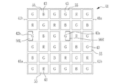
- the color filter 41 has a long periodicity with a color arrangement of 6 ⁇ 6 pixels as one unit. More specifically, the color filter 41 is an array in which two types of subunits 41a and 41b each having a color array of 3 ⁇ 3 pixels are arranged at diagonal positions. In the first subunit 41a, a green (G) filter is arranged at the center and diagonal positions of 3 ⁇ 3 pixels, a blue (B) filter is arranged at the center of the left and right, and a red (R) filter is arranged at the center of the top and bottom. Is a unit.
- G green
- B blue
- R red
- the second subunit 41b is similar to the first subunit 41a in that G filters are arranged at the center and diagonal positions of 3 ⁇ 3 pixels, but the B filter and the R filter are the first subunit 41a.
- the R filter is arranged at the center of the left and right, and the B filter is arranged at the center of the top and bottom.
- the color filter 41 shown in FIG. 2 has a long periodicity as compared with a Bayer arrangement in which the color arrangement of 2 ⁇ 2 pixels is one unit, so that the occurrence of moire can be suppressed without using an optical low-pass filter. it can. Further, in the solid-state imaging device 10 employing the color filter 41, since RGB pixels always exist in the vertical direction (vertical direction) and the horizontal direction (horizontal direction), false colors can be suppressed and accurate color reproduction is possible. is there.
- the phase difference pixels 42 a and 42 b are for obtaining a signal including information on parallax for the phase difference AF, and are arranged in place of the normal pixel 43.
- the lower left G pixel of the upper right first subunit 41a and the upper left second subunit 41b is formed.
- the opening 55 of the normal pixel 43 is formed so as to be symmetrical in the vertical and horizontal directions, and receives the light incident from the vertical and horizontal directions equally (isotropically).
- the right phase difference pixel 42a selectively receives light that has reached the right side of the PD 22 among the incident light, so that the opening 56R is smaller than the opening 55 of the normal pixel 43, and from the center of the PD 22. It is arranged eccentric to the right.
- the left phase difference pixel 42b has an opening 56L smaller than the opening 55 of the normal pixel 43 and is eccentrically arranged to the left in order to selectively receive the incident light that has reached the left side of the PD 22. .
- the pixel signals of the phase difference pixels 42a and 42b are signals having left and right parallax, respectively, and are used for phase difference AF.
- the imaging signal is formed by the normal pixel 43
- the pixel signal at the position where the phase difference pixels 42a and 42b exist is lost. Therefore, this missing pixel signal is created by interpolation processing from G pixels (normal pixels 43) around the phase difference pixels 42a and 42b.
- the phase difference pixels 42 a and 42 b are used for the imaging signal, the pixel signal is amplified to match the sensitivity with the normal pixel 43.
- phase difference pixels 42 a and 42 b are provided on the entire surface of the light receiving region 11, the phase difference pixels 42 a and 42 b are not necessarily provided in the 6 ⁇ 6 pixel unit of the color filter 41.
- the phase difference pixels 42a and 42b are not provided in the 6 ⁇ 6 pixel unit of the color filter 41.
- the phase difference pixels 42a and 42b are not provided in the unit in which the phase difference pixels 42 a and 42 b are not provided.
- the phase difference pixels 42a and 42b are provided, the phase difference pixels 42a and 42b are provided at the above-mentioned locations in the 6 ⁇ 6 pixel unit.
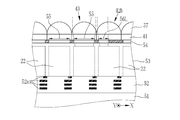
- the solid-state imaging device 10 is a backside illuminated (BSI) CMOS image sensor, and includes a support substrate 51, a wiring layer 52, a p-type semiconductor substrate 53, a light shielding layer 54, and a color filter. 41, a microlens 57, and the like.
- the side on which the wiring layer 52 is provided with respect to the p-type semiconductor substrate 53 is the “front surface” of the solid-state imaging device 10, and the side on which the color filter 41, the light shielding layer 54, and the microlens 57 are provided is the “back surface”.
- FIG. 3 schematically shows a cross section of the solid-state imaging device 10 in the central portion 11a (see FIG. 4) of the light receiving region 11.
- the support substrate 51 is, for example, a silicon substrate, and exposes the back surface of the p-type semiconductor 53 in the process of manufacturing the back-illuminated solid-state imaging device 10, and the surface of the wiring layer 52 to thin the p-type semiconductor 53. To be joined.
- the wiring layer 52 is formed on the surface of the p-type semiconductor substrate 53, and the transistors (Tr23, Ta24) that form each pixel 21 (the normal pixel 43 and the phase difference pixels 42a, 42b) by the wiring 52a provided in the wiring layer 52.
- Ts25 various circuits such as a vertical scanning circuit 13, a horizontal scanning circuit 14, a control circuit 17, an output circuit 16, a control circuit 17, and a CDS 31 for driving each pixel 21, a reset line 26, a signal line 27, a row
- Various wirings such as a selection line 28 and an output bus line 33 are formed.
- the PD 22 is formed by a PN junction of a p-type semiconductor substrate 53 and an n-type semiconductor region formed in the p-type semiconductor substrate 53.
- the p-type semiconductor substrate 53 is thinned, and the photoelectric conversion region of the PD 22 indicated by a broken line reaches the vicinity of the back surface of the p-type semiconductor substrate 53.
- the charges generated by the photoelectric conversion of the PD 22 are accumulated in the vicinity of the interface with the wiring layer 52.
- Each PD 22 is separated by a separation layer (for example, p ++ layer) not shown.
- the light shielding layer 54 is provided on the back side of the p-type semiconductor substrate 53, and suppresses color mixing by shielding light incident between the PDs 22.
- the light shielding layer 54 is formed of, for example, a metal thin film and has openings 55 and 56 corresponding to the PDs 22.
- the openings 55 and 56 are filled with, for example, a transparent material, and the back surface of the light shielding layer 54 (interface with the color filter 41) is flat.
- the opening 55 is provided in the normal pixel 43 and has a size that exposes almost the entire surface of the PD 22 of the normal pixel 43. For this reason, as indicated by the alternate long and short dash line, in the normal pixel 43, almost the entire light flux of the light incident through the corresponding microlens 57 and the color filter 41 is incident on the PD 22 through the opening 55.
- the opening 55 has the same size in all the normal pixels 43 regardless of the position of the normal pixels 43 and the like. For this reason, all the normal pixels 43 have the same light receiving area regardless of the position in the light receiving region 11 (see FIG. 4).
- the opening 56L is provided in the left phase difference pixel 42b, is narrower than the opening 55 of the normal pixel 43, and has a small opening area. Further, the opening 56L is eccentrically arranged on the left side (upstream side in the X direction). For this reason, in the left phase difference pixel 42b, the light incident through the corresponding microlens 57 and the color filter 41 passes through the opening 56L and reaches the left side of the PD 22 (the side on the upstream in the X direction). Only a part of the light beam is received.
- the opening 56R is eccentrically arranged on the right side (downstream in the X direction), and the corresponding microlens 57 and Of the light incident through the color filter 41, light that reaches the right side (the side that is downstream in the X direction) of the PD 22 through the opening 56R is received.
- Each color segment of the color filter 41 is provided corresponding to the PD 22, and the center of each color segment is at a position corresponding to the center of the PD 22.
- the light collected by the microlens 57 passes through the color filter 41 and only one of R, G, and B color light enters the PD 22.
- the microlens 57 is provided on the color filter 41 so as to correspond to each PD 22 and has a substantially hemispherical shape.
- the microlens 57 collects incident light on the corresponding PD 22.
- the center of the microlens 57 substantially coincides with the center of the PD 22, but is decentered toward the center of the light receiving region 11 according to the distance from the center.
- the microlens 57 is also arranged (scaled) in the central portion 11 a while being offset in the central direction of the light receiving region 11 according to the principal ray angle 45.
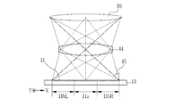
- an imaging lens 44 is disposed in front of the solid-state imaging device 10 and forms an image of the subject 59 in the light receiving region 11.
- the imaging lens 44 is schematically represented by a single optical lens, but actually includes a plurality of optical lenses.
- the imaging lens 44 may include various optical filters such as an infrared filter and an optical element having substantially no lens action.
- the chief ray angle (hereinafter referred to as chief ray angle) 45 indicated by a one-dot chain line is from the central portion 11a of the light receiving region 11 to the left peripheral portion 11bR. , And gradually increases toward the right peripheral portion 11bL. For this reason, each pixel 21 has a structure in accordance with the principal ray angle 45 of each location.
- the left peripheral portion 11bR is a rectangular region located upstream in the X direction.
- the right peripheral portion 11bL is a rectangular region located downstream in the X direction.
- the central portion 11a is a rectangular region located between the left peripheral portion 11bR and the right peripheral portion 11bL.
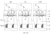
- the microlens 57 is scaled according to the chief ray angle 45. Specifically, the structure from the color filter 41 to the photodiode 22 is the same in both the central portion 11a and the peripheral portions 11bR and 11bL. However, in the peripheral portions 11bR and 11bL, the center of each microlens 57 is provided. The position is eccentrically arranged on the central portion 11a side.
- the incident light to each normal pixel 43 is a right half light beam (hereinafter referred to as a right light beam) indicated by a dashed arrow, and a left half light beam (hereinafter referred to as a left light beam) indicated by a solid arrow.
- the left lens is focused on the right side of the PD 22 and the right beam is focused on the left side of the PD 22 by the microlens 75. That is, in the normal pixel 43 in the central portion 11a, almost all of the incident light beam is collected on the PD 22.
- the normal pixel 43 in the right peripheral portion 11bR the chief ray is inclined as shown by the alternate long and short dash line, but since the microlens 75 is scaled according to the angle of the chief ray, the left beam is also on the right side. All the light beams are also condensed on the PD 22. Similarly, the same applies to the normal pixel 43 in the left peripheral portion 11bL. Since the microlens 75 is scaled according to the angle of the principal ray, both the left beam and the right beam are condensed on the PD 22. Therefore, the normal pixel 43 can receive almost all of the luminous flux of incident light by the PD 22 in any of the central portion 11a, the right peripheral portion 11bR, and the left peripheral portion 11bL.
- phase difference pixels 42 a and 42 b the microlens 57 is scaled in accordance with the chief ray angle 45 as in the normal pixel 43.
- the phase difference pixels 42 a and 42 b are adjusted in accordance with the position in the light receiving region 11 in addition to the openings 56 ⁇ / b> L and 56 ⁇ / b> R being shifted to one side.
- the openings 56L and 56R of the phase difference pixels 42a and 42b have the same size in each of the central portion 11a, the right peripheral portion 11bR, and the left peripheral portion 11bL (an area half of the opening 55 of the normal pixel 43). ) Is explained.
- the left half of the right phase difference pixel 42a in the central portion 11a is shielded from light, only light that reaches the right side of the PD 22 through the opening 56R is selectively selected. Receive light. For example, when about 1/5 of the left beam and about 4/5 of the right beam reach the right side of the PD 22, the amount of light received by the right phase difference pixel 42a in the central portion 11a is about 1/2 of the incident light amount. It is.
- the right phase difference pixel 42a in the right peripheral portion 11bR most of the right light beam (broken arrow) having a small incident angle is shielded from the light beam of incident light, and the left light beam (solid line arrow) having a large incident angle. Almost reaches the PD 22. For example, when about 1/5 of the right beam and almost all of the left beam reach the right side of the PD 22, the amount of light received by the right phase difference pixel 42a in the right peripheral portion 11bR is about 3/5 of the incident light amount.
- the incident angle of the right light beam (broken arrow) out of the light beams of the incident light is large, and the left light beam (solid line) The incident angle of (arrow) is small.
- the right phase difference pixel 42a in the left peripheral portion 11bL almost all of the right beam is blocked and a part of the left beam reaches the PD 22.
- the amount of light received by the right phase difference pixel 42a in the left peripheral portion 11bL is about 2/5 of the incident light amount.
- the specific sensitivity of the right phase difference pixel 42a (sensitivity to the sensitivity of the normal pixel 43) is substantially proportional to the position in the X direction, and is larger in the right peripheral portion 11bR than in the central portion 11a.
- the left peripheral portion 11bL is smaller than that of the central portion 11a.
- the phase difference AF can be performed with higher accuracy than when the pixel of the center portion 11a is used.
- the accuracy of the phase difference AF is not good.
- the opening 56R of the right phase difference pixel 42a located in the left peripheral portion 11bL from the center of the light receiving region 11 (center line of the central portion 11a) is changed to the openings of the central portion 11a and the right peripheral portion 11bR.
- the area is larger than 56R.
- the left light beam (solid arrow) that is partially shielded from light enlarges the aperture area as shown in FIG. Almost everything reaches the PD 22.
- the right light beam (broken arrow) that has been shielded from light passes through the opening 56R having an enlarged area and reaches the PD 22.
- the amount of light received by the phase difference pixel 42a of the left peripheral portion 11bL having the opening 56R whose area is enlarged is improved to about 3/5 of the incident light amount. .
- the magnification ratio of the opening 56R in the left peripheral portion 11bL is such that the specific sensitivity is symmetrical from the center line of the central portion 11a to the left peripheral portion 11bL and from the center line to the right peripheral portion 11bR. Further, the adjustment may be made according to the position of each right phase difference pixel 42a.
- the enlargement ratio of the opening 56R in the left peripheral portion 11bL is adjusted so that the specific sensitivity of the right phase difference pixel 42a in the left peripheral portion 11bL is at least equal to or higher than the specific sensitivity of the right phase difference pixel 42a in the central portion 11a. It only has to be.
- FIG. 10 the magnification ratio of the opening 56R in the left peripheral portion 11bL is such that the specific sensitivity is symmetrical from the center line of the central portion 11a to the left peripheral portion 11bL and from the center line to the right peripheral portion 11bR.
- the adjustment may be made according to the position of each right phase difference pixel 42a.
- the enlargement ratio of the opening 56R is adjusted so that the specific sensitivity is constant from the center of the light receiving region 11 to the left peripheral portion 11bL.
- the enlargement ratio of the opening 56R is adjusted so that the specific sensitivity at the center of the light receiving region 11 is equal to the specific sensitivity of the left peripheral portion 11bL, the right phase difference pixel 42a of the left peripheral portion 11bL. Since there is a large amount of left beam (signal) that should originally be received and the amount of light received by the right beam that is noisy is small, the specific sensitivity can be increased while maintaining good S / N.
- the opening 56R of the right phase difference pixel 42a in the right peripheral portion 11bR may be smaller than that in the central portion 11a.
- the reduction ratio of the opening 56R in the right peripheral portion 11bR is preferably adjusted so that the specific sensitivity is constant from the center of the light receiving region 11 to the right peripheral portion 11bR as shown in FIG.
- the area of the opening 56R is adjusted so that the specific sensitivity at the center of the light receiving region 11 and the specific sensitivity of the right peripheral portion 11bR are equal to each other, compared with the case where the opening area is the same as that at the center. In this case, the specific sensitivity is lowered, but the S / N can be improved.
- the area of the opening 56R is adjusted so that the specific sensitivity is substantially equal in the central portion 11a, the left peripheral portion 11bL, and the right peripheral portion 11bR. Needless to say, it is particularly preferable.
- the cross section of the left phase difference pixel 42b is symmetrical to the right phase difference pixel 42a. Therefore, as shown in FIG. 14, the area of the opening 56L of the left phase difference pixel 42b increases at least from the center of the light receiving region 11 to the right peripheral portion 11bR, contrary to the case of the right phase difference pixel 42a described above.
- the opening area is adjusted as follows.
- the specific sensitivity of the left phase difference pixel 42b on the right peripheral portion 11bR is lower than that of the central portion 11a (one point). Indicated by a chain). However, by expanding the opening area of the left phase difference pixel 42b on the right peripheral portion 11bR, the left phase difference pixel 42b on the right peripheral portion 11bR is the same as the left phase difference pixel 42b on the left peripheral portion 11bL. Specific sensitivity is improved to the extent (shown by a solid line) or to the same extent as the center of the central portion 11a (shown by a broken line).
- the opening 56R of the right phase difference pixel 42a is enlarged at the left peripheral portion 11bL, and the right peripheral portion 11bR is the same as or reduced at the central portion 11a.
- the opening 56L of the left phase difference pixel 42b is enlarged at the right peripheral portion 11bR, and the left peripheral portion 11bL is the same as or reduced at the central portion 11a.
- the phase difference pixel (right In the right phase difference pixel 42a on the peripheral portion 11bR and the left phase difference pixel 42b) on the left peripheral portion 11bL, the amount of received light of the light beam that becomes noise increases, so the S / N deteriorates and the specific sensitivity is high.
- the accuracy of the phase difference AF may deteriorate.
- the left and right phase difference pixels 42a and 42b adjust the sizes of the openings 56L and 56R according to the positions, the accuracy of the phase difference AF is surely improved without deteriorating the S / N. Can be improved.
- the microlens 75 of the phase difference pixels 42a and 42b is scaled differently from the normal pixel 43, color mixing may occur and the quality of the captured image may be impaired.
- the accuracy of the phase difference AF is improved by adjusting the aperture areas of the phase difference pixels 42a and 42b without scaling the microlens 75 differently from the normal pixel 43. The image quality is not impaired.
- the opening area of the right phase difference pixel 42a is adjusted as described above, for example, as shown in FIG. 16, in the left peripheral portion 11bL, the right side of the opening 56R of the right phase difference pixel 42a in the central portion 11a
- the area may be enlarged by moving the left end position of the phase difference pixel 42a to the left and expanding it to the side of the opening 56R.
- both S / N and improvement in specific sensitivity are achieved. Easy to make.
- the base line length (the distance between the centers of the pair of phase difference pixels 42a and 42b) is not easily shortened, so that information on parallax can be easily obtained.
- the right phase difference pixel 42a is taken as an example, but the same applies to the left phase difference pixel 42b.
- the left end position is aligned with that of the central portion 11a, and the right end position is set to the right side.
- the area may be expanded by moving to and expanding the opening 56L laterally.
- both the right end and the left end of the opening 56R of the right phase difference pixel 42a in the center portion 11a are moved to the left side to enlarge the opening area. May be.
- the center position of the opening 56R also moves to the left.
- the opening area can be expanded so as to prevent the right side light flux that becomes noise from entering.
- the left phase difference pixel 42b is the same as the left phase difference pixel 42b.
- the PD 22 of the right phase difference pixel 42a in the left peripheral portion 11bL is made smaller than the PD 22 in the central portion 11a as shown in FIG. May be.
- the distance of the PD 22 of the right phase difference pixel 42a from the PD 22 of the normal pixel 43 next to it is increased.
- the distance between the PD 22 of the normal pixel 43 and the PD 22 of the right phase difference pixel 42a is short, light obliquely incident on the normal pixel 43 may leak into the PD 22 of the right phase difference pixel 42a and color mixing may occur.
- the PD 22 of the right phase difference pixel 42a is made small, even if light obliquely incident on the normal pixel 43 leaks to the phase difference pixel 42a side, the PD 22 of the right phase difference pixel 42a Since it is difficult to reach, color mixing is more reliably prevented and a signal with good S / N is easily obtained.
- the area of the opening 56R and the size and shape of the PD 22 may be appropriately determined so that the specific sensitivity and S / N are optimized.
- the size and shape of the PD 22 may be a rectangle matching the enlarged opening 56R of the right phase difference pixel 42a.
- it may be a rectangle whose size and shape substantially match the opening 56R of the right phase difference pixel 42a. The same applies to the left phase difference pixel 42b.
- the light receiving area is divided into the central part 11a and the peripheral parts 11bL and 11bR, but the light receiving area 11a may be further divided.
- the light receiving region 11 is divided into a left central portion 81aL, a right central portion 81aR, an inner left peripheral portion 81bL, an inner right peripheral portion 81bR, an outer left peripheral portion 81cL, and an outer right peripheral portion 81cR.
- the inner left peripheral portion 81bL, the inner right peripheral portion 81bR, the outer left peripheral portion 81cL, and the outer right peripheral portion 81cR have a channel shape, but may be a rectangle extending in the vertical direction.
- predetermined various processing methods such as shading correction of a captured image and flaw correction (correction of pixel values of the phase difference pixels 42a and 42b) may vary depending on the position of the light receiving region 11, the light receiving region 11 is changed as described above. In the case of fine division, it is preferable to divide the light receiving region 11 according to the division of various processing methods.
- the opening area of the right phase difference pixel 42a may be enlarged stepwise in the order of the left central portion 81aL, the inner left peripheral portion 81bL, and the outer left peripheral portion 81cL.
- the opening area of the right phase difference pixel 42a is increased stepwise in accordance with different processing methods, the opening area is smoothly enlarged according to the distance from the center (see FIG. 9).
- good processing results can be easily obtained. That is, the stepwise expansion of the opening area of the right phase difference pixel 42a makes it easy to improve both the accuracy of the phase difference AF and the image quality of the captured image.
- the opening area of the right phase difference pixel 42a is the same in the right central portion 81aR, the inner right peripheral portion 81bR, and the outer right peripheral portion 81cR.
- the left phase difference pixel 42b may have an opening area that is gradually increased at the right center portion 81aR, the inner right peripheral portion 81bR, and the outer right peripheral portion 81cR. Even when the light receiving region 11 is divided into the central portion 11a and the peripheral portions 11bL and 11bR, the opening area may be enlarged stepwise.
- the chief ray angle 45 at each position changes depending on the zoom magnification, and thus the aperture areas of the phase difference pixels 42a and 42b at each position may not be uniquely determined.
- the imaging lens 44 is at the telephoto end (when the focal length is the longest), the wide angle end (when the focal length is the shortest), or an intermediate position thereof, the chief ray angle 45 from the infinity distance is set.
- the error at the wide-angle end (deviation of specific sensitivity, etc.) is large.
- the aperture area of each of the phase-difference pixels 42a and 42b is adjusted in accordance with the principal ray angle 45 at the intermediate position between the telephoto end and the wide-angle end. It is particularly preferable to define.
- the G pixels are the phase difference pixels 42a and 42b.
- the R pixel and the B pixel may be the phase difference pixels 42a and 42b.
- all the phase difference pixels 42a and 42b may be formed by R pixels, or all the phase difference pixels 42a and 42b may be formed by B pixels.
- any two of R, G, and B may be used as the phase difference pixels 42a and 42b.
- the phase difference pixels 42a and 42b are two or more colors of R, G, and B
- the amount of decrease in sensitivity in the peripheral portion 11b is different for each color, so the openings of the phase difference pixels 42a and 42b are different for each color.
- the area enlargement ratio For example, the enlargement ratio of the opening area of the phase difference pixels 42a and 42b of each color is set to B pixel> G pixel> R pixel, although it depends on the focal length of the micro lens 75 and the like.
- the reference for the enlargement ratio is the opening area of each color phase difference pixel 42a, 42b in the central portion 11a. In this way, if the enlargement ratio of the opening area of the phase difference pixels 42a and 42b is adjusted for each color, a signal having a good S / N can be obtained in the phase difference pixels 42a and 42b of each color. Easy to improve accuracy.
- the pixels of the solid-state imaging device 10 are squarely arranged, but the pixel arrangement is arbitrary.
- the pixel arrangement may be a honeycomb arrangement as shown in FIGS.
- the color arrangement of the color filter when the pixel arrangement is the honeycomb arrangement is arbitrary, but for example, the color arrangement shown in FIGS. 22 and 23 can be used.
- the color arrangement in FIG. 22 is an example in which columns of G pixels and columns in which two R pixels and two B pixels are alternately arranged are alternately arranged in a 45-degree oblique direction.
- the color filter 41 with 6 ⁇ 6 pixels as a unit is used, the arrangement of the color filters 41 is arbitrary.
- the pixels are arranged in a square array, as shown in FIG. 24, a so-called Bayer array in which 2 ⁇ 2 pixels surrounded by a broken line are arranged vertically and horizontally may be used.
- the phase difference pixels 42a and 42b are formed in the lower left G pixel of the upper right first subunit 41a and the lower left G pixel of the upper left second subunit 41b within the 6 ⁇ 6 pixel unit of the color filter 41.
- the position of the G pixel forming the phase difference pixels 42a and 42b is arbitrary.
- the center G pixel of the upper right first subunit 41a and the center G pixel of the upper left second subunit 41b may be used as the phase difference pixels 42a and 42b, respectively.
- the G pixel of the lower right second subunit 41b and the G pixel of the lower left first subunit 41a may be used as the phase difference pixels 42a and 42b.
- the pair of phase difference pixels 42a and 42b are provided in the same row, but they may be provided in different rows.
- the phase difference pixels 42a and 42b are formed asymmetrically in the X direction (horizontal direction), and the phase difference pixels 42a and 42b acquire the left and right (horizontal direction) parallax, but the Y direction (vertical direction) and the diagonal direction
- the parallax information may be acquired.
- the phase difference pixel structure (the position of the opening) may be asymmetric in the vertical direction, and the paired phase difference pixels may be arranged vertically to obtain vertical parallax.
- a pair of phase difference pixels having an asymmetric structure in the oblique direction may be arranged in the oblique direction.
- phase difference pixels 42a and 42b for obtaining parallax in the X direction phase difference pixels for obtaining parallax in the Y direction, and phase difference pixels for obtaining parallax in the oblique direction are provided in the light receiving region 11. It may be left.
- the phase difference pixels in these directions are also the same as the left and right phase difference pixels 42a and 42b in the above-described embodiment.
- the opening is preferably enlarged in accordance with the direction of the received light beam and the position in the light receiving region 11.
- the plurality of phase difference pixels 42a and 42b are uniformly arranged in the light receiving region 11, but the number, arrangement and distribution of the phase difference pixels 42a and 42b are arbitrary.
- the phase difference pixels 42a and 42b are arranged in a part of the light receiving region 11, but as shown in FIG. 25, all the pixels may be phase difference pixels 42a and 42b. .
- all the pixels are phase difference pixels 42a and 42b, for example, a 3D image can be obtained with a single eye (one solid-state imaging device).
- the pixels are arranged in a square pattern, but the pixels may be arranged in a honeycomb pattern.
- the color filter may be a Bayer array.
- Three transistors Tr23, Ta24, and Ts25 are used for one pixel. If incident light can be photoelectrically converted and a pixel signal necessary for formation of a captured image and phase difference AF can be output,
- the number of transistors and the like are arbitrary. For example, a transfer transistor may be added between the PD 22 and the FD.
- the light shielding layer 54 and the color filter 41 are laminated, even if the light shielding layer 54 and the color filter 41 are integrally formed by embedding each color segment of the color filter 41 in the openings 55 and 56 of the light shielding layer 54. Good.
- the light shielding layer 54 and the color filter 41 are sequentially laminated on the back surface of the p-type semiconductor substrate 53, the order of lamination of the light shielding layer 54 and the color filter 41 may be reversed.
- a complementary color filter may be used.
- the color filter of this specification includes an ND filter, and the phase difference pixels 42a and 42 may be provided with this ND filter.
- the openings 55 and 56 of the light shielding layer 54 are filled with a transparent material to flatten the light shielding layer 54, the openings 55 and 56 may be filled with the material of the color filter 41.
- the light shielding layer 54 a light shielding material is also provided between the normal pixels 43 and the openings 55 of the normal pixels 43 are separated. However, the light shielding material between the normal pixels 43 is not provided, and the openings 55 of the normal pixels 43 are not provided. All may be continued. In this case, the light shielding layer 54 is formed by arranging a light shielding material only in a portion that restricts incident light in the phase difference pixels 42a and 42b.
- the solid-state imaging device 10 is a CMOS image sensor, but may be a CCD image sensor.
- the solid-state imaging device 10 is a back-side illuminated image sensor, but may be a front-side illuminated (FSI) image sensor.
- FSI front-side illuminated
- the solid-state imaging device of the present invention is suitable for a camera module mounted on a thin digital camera, a mobile phone, a PDA, a smart photon, or the like.
- the combination of the imaging lens 44 with a short back focus and a solid-state imaging device with a wide light receiving area is suitable for a camera or a camera module having a large principal ray angle in the periphery.
- Solid-state imaging device 11 Light receiving area 11a Center part 11bL Left peripheral part 11bR Right peripheral part 21 Pixel 42a Right phase difference pixel 42b Left phase difference pixel 43 Normal pixel 55, 56L, 56R Aperture
Landscapes
- Physics & Mathematics (AREA)
- Engineering & Computer Science (AREA)
- Multimedia (AREA)
- Signal Processing (AREA)
- Spectroscopy & Molecular Physics (AREA)
- General Physics & Mathematics (AREA)
- Optics & Photonics (AREA)
- Automatic Focus Adjustment (AREA)
- Solid State Image Pick-Up Elements (AREA)
- Transforming Light Signals Into Electric Signals (AREA)
- Focusing (AREA)
Abstract
撮影画像の画質を低下することなく、中央部と周辺部での位置による位相差画素の感度差を低減する固体撮像装置を提供する。 固体撮像装置(10)の受光領域(11)には、複数の通常画素(43)と、複数の右位相差画素(42a)と、複数の左位相差画素(42b)とが配置されている。受光領域(11)は、中央部(11a)と、右周辺部(11bR)と左周辺部(11bL)に区画される。右位相差画素(42a)の開口(56R)は、左周辺部(11bL)のものが、中央部(11a)及び右周辺部(11bR)のものよりも面積が大きい。左位相差画素(42b)の開口(56L)は、右周辺部(11bR)ものが、中央部(11a)及び左周辺部(11bL)のものよりも面積が大きい。
Description
本発明は、位相差検出方式の焦点調節が可能な固体撮像装置に関する。
デジタルカメラや、携帯電話機及びスマートフォン等の携帯電子機器のカメラモジュールには、オートフォーカス機能が標準的に備えられている。このオートフォーカス機能には、像のコントラストが最大になるように焦点調節を行うコントラスト検出方式(いわゆるコントラストAF)や、視差による位相差に基づいて焦点調節を行う位相差検出方式のオートフォーカス(以下、位相差AFという)等がある。
位相差AFを実行する固体撮像装置は、例えば特許文献1に記載されているように、複数の通常画素が配列された受光領域内の所定箇所に、左右いずれかの方向から入射する光を選択的に受光する2種類の位相差画素が配置されている。
ところで、近年のデジタルカメラやカメラモジュールは、小型化、薄型化の要請から、バックフォーカスの短い撮像レンズが用いられ、また受光領域の面積が大きい固体撮像装置が用いられるようになってきている。このように、短いバックフォーカスに対して受光領域の面積が大きいと、受光領域の周辺部への光の入射角度が大きくなる。
固体撮像装置の画素は、概ね正面から入射する光を効率良く集光して光電変換するように構成されているので、光の入射角度が大きくなると感度が低下する。このため、受光領域の周辺部にある画素への光の入射角度が大きい場合に、受光領域上に形成される画像に、輝度や色にシェーディングが生じることがある。シェーディングを低減するためには、周辺部への光の入射角度を考慮して、中央部と周辺部の間で、画素の感度を均一化すればよい。例えば、各画素に設けられるマイクロレンズを、周辺部の画素ほど中央部に寄せて配置(スケーリング)することにより、周辺部にある画素の集光効率を上げ、中央部の画素と周辺部の画素の間で感度差を緩和して、シェーディングを低減する技術が知られている。
また、受光領域の中央部から周辺部にかけて画素の開口を大きくすることにより、あるいは周辺部から中央部にかけて画素の開口を小さくすることにより、中央部と周辺部の間で画素の感度を均一化して、シェーディングを低減する技術も知られている(特許文献2)。
さらに、位相差画素を有する固体撮像装置においては、中央部の位相差画素の瞳領域を周辺部のものに比べて小さくすることによって、各位相差画素の信号レベルを均一にすることや、逆に周辺部の位相差画素の瞳領域を中央部のものに比べて小さくして、各位相差画素のケラレを均一化することで、位相差AFの精度を向上させる技術が知られている(特許文献3)。
各位相差画素は、例えば左右に非対称な構造に形成されているので、通常画素よりも光の入射角度に対して敏感であり、周辺部にある位相差画素は、通常画素よりも感度の低下が大きい。通常画素は、例えばマイクロレンズのスケーリング等によって感度の均一化を図ることができるが、上述のように周辺部における位相差画素の感度の低下量は、通常画素よりも大きいので、マイクロレンズのスケーリングでは位相差画素の感度を十分に補えない。また、周辺部の位相差画素を用いる場合には、位相差AFの精度が悪くなることがある。
このため、周辺部の位相差画素を用いる場合でも、精度が良い位相差AFを行うためには、例えば特許文献2,3に倣って周辺部の位相差画素の開口や瞳領域の大きさを調節し、周辺部の位相差画素の感度を向上させることが望ましい。
しかしながら、各位相差画素は、非対称な構造をしているので、特許文献2,3のように、受光領域の周辺部にある位相差画素の開口等を一律に大きくしても、位相差AFの精度が向上しない場合がある。具体的には、左方向から入射して画素の右側部に到達した光を選択的に受光する右位相差画素は、受光領域の中央に対して、受光領域の左側の周辺部にあるものは感度が低いが、受光領域の右側の周辺部にあるものではむしろ感度が高い。逆に、右方向から入射して画素の左側部に到達した光を選択的に受光する左位相差画素は、右側の周辺部にあるものでは感度が低いが、左側の周辺部にあるものでは感度が高い。したがって、特許文献2,3のように、周辺部において開口や瞳領域の大きさを調節しても、右位相差画素と左位相差画素の区別をせずに、位相差画素の開口等の大きさを一律に調節したのでは、もともと感度が高い側にあるものではS/Nが悪化してしまうので、必ずしも位相差AFの精度向上には繋がらない。
また、画素の信号電荷を画素信号(電圧信号)として読み出す場合に、通常画素の画素信号を読み出す場合よりもゲインを上げることによって、感度が低い周辺部の位相差画素の画素信号を大きくし、各位相差画素の感度を均一化させることもできる。しかし、読み出しのゲインを上げると、画素信号に含まれるノイズ成分も増大してしまうのでS/Nは改善しない。特に、周辺部の画素では、光の入射角度が大きいために、本来入射すべき光が隣接する画素に入射されて、混色が発生することがある。この混色による画素号は、読み出しのゲインを上げると大きくなるので、感度が低い周辺部の位相差画素の画素信号を読み出す場合に、にゲインを上げるだけでは、位相差AFの精度を十分に改善することはできない。
この他には、マイクロレンズのスケーリング量を、通常画素と位相差画素とで変えることによって、周辺部の位相差画素の感度を向上させることも考えられる。しかし、通常画素と位相差画素との間でマイクロレンズのスケーリング量を変えると、通常画素のマイクロレンズと位相差画素のマイクロレンズの間に隙間が生じるために、混色が増大してしまうことがある。
本発明は、撮影画像の画質を低下させずに、受光領域の周辺部にある位相差画素の感度を向上して、正確な位相差AFを行える固体撮像装置を提供することを目的とする。
上記目的を達成するために、本発明の固体撮像装置は、第2周辺部に存在する第1位相差画素は、中央部及び第1周辺部に存在する第1位相差画素に対して、第1開口の面積が大きく、そして第1周辺部に存在する第2位相差画素は、中央部及び第2周辺部に存在する第2位相差画素に対して、第2開口の面積が大きい。固体撮像装置の受光領域には、複数の通常画素と、複数の第1位相差画素と、複数の第2位相差画素とが配列されている。通常画素は、入射光を等方的に受光する。第1位相差画素は、第1方向に偏心配置された第1開口を有し、この第1開口を通って、第1方向での下流側に到達した光を選択的に受光する。第2位相差画素は、第1方向とは逆の第2方向に偏心配置された第2開口を有し、この第2開口を通って、第2方向での下流側に到達した光を選択的に受光する。被写体の像が形成される受光領域は、第1周辺部、第2周辺部、中央部に区画されている。第1周辺部は、第1方向での下流側にある周辺部である。第2周辺部は、第1方向での上流側にある周辺部である。中央部は、第1周辺部と第2周辺部との間に存在する。
第2周辺部に存在する第1位相差画素の第1開口は、中央部に存在する第1位相差画素の第1開口に対して、第2方向に拡張されていることが好ましい。第1周辺部に存在する第2位相差画素の第2開口は、中央部に存在する第2位相差画素の第2開口に対して、第1方向に拡張されていることが好ましい。
第2周辺部に存在する第1位相差画素の第1開口の中心位置は、中央部に存在する第1位相差画素の第1開口に対して、第2方向に寄っているのが好ましい。第1周辺部に存在する第2位相差画素の第2開口の中心位置は、中央部に存在する第2位相差画素の第2開口に対して、第1方向に寄っていることが好ましい。
第2周辺部に存在する第1位相差画素及び第1周辺部に存在する第2位相差画素のフォトダイオードは、中央部に存在する第1位相差画素及び第2位相差画素のフォトダイオードよりも受光面積が小さいことが好ましい。
第1開口の面積は、中央部から第2周辺部に向かって拡大され、第2開口の面積は、中央部から第1周辺部に向かって拡大されていることが好ましい。
第1及び第2位相差画素は、3原色の色光を光電変換するために、各色光に対応して3種類がある。中央部から第2周辺部に向かって拡大される第1開口の拡大率と、中央部から第1周辺部に向かって拡大される第2開口の拡大率は、画素の色光の種類に応じて決められていることが好ましい。
固体撮像装置の前に配置されるズームレンズが望遠端と広角端との中間位置にセットされたときに、無限遠からの被写体光がズームレンズを出射するときの出射角度に基づいて、第2周辺部に存在する第1位相差画素の第1開口と、第1周辺部に存在する第2位相差画素の第2開口の面積がそれぞれ定められていることが好ましい。
第1周辺部に存在する第1位相差画素は、中央部に存在する第1位相差画素に対して、第1開口が小さく、そして第2周辺部に存在する第2位相差画素は、中央部に存在する第2位相差画素に対して、第2開口が小さいことが好ましい。
通常画素、第1位相差画素、及び第2位相差画素は、入射光を集光するマイクロレンズを有することが好ましい。第1及び第2周辺部に存在する通常画素、第1位相差画素、及び第2位相差画素の各マイクロレンズは、入射光の入射角度に応じて、中央部に向かって偏心して配置するのが好ましい。
本発明の固体撮像装置は、被写体の像が形成される受光領域に、第1及び第2位相差画素だけが配置されている。
本発明によれば、第2周辺部に存在する第1位相差画素は、中央部及び第1周辺部に存在する第1位相差画素に対して、第1開口の面積が大きくし、また第1周辺部に存在する第2位相差画素は、中央部及び第2周辺部に存在する第2位相差画素に対して、第2開口の面積が大きくしてある。これにより、第1及び第2の位相差画素の感度を適切に補い、位相差AFの精度を向上させることができる。また、周辺部に存在する位相差画素に対して、マイクロレンズのスケーリングによって感度補正を行っていないので、撮影画像の画質を低下させることもない。
図1に示すように、固体撮像装置10はCMOS型イメージセンサであり、受光領域11と、垂直走査回路13、水平走査回路14、出力回路16、制御回路17等を備える。
受光領域11には、複数の画素21が水平方向(X方向)及び垂直方向(Y方向)に沿って正方配列されている。この受光領域11には、撮像レンズ(図3参照)によって被写体の像が結像され、各画素21は光電変換によって入射光量に応じた電荷を発生する。
画素21は、フォトダイオード(以下、PDという)22、リセットトランジスタ(以下、Trという)23、アンプトランジスタ(以下、Taという)24、選択トランジスタ(以下、Tsという)25を備えている。Tr23,Ta24,Ts25は、例えばn型のMOSトランジスタである。また、各画素21には、赤色(R),緑色(G),青色(B)のいずれかのカラーフィルタ41(図2参照)が設けられており、カラーフィルタ41の色と同じ色光を光電変換する。
画素21には、通常画素と位相差画素の2種類がある。通常画素と位相差画素は、立体的構造(具体的にはPD22に対する開口の大きさや位置)が異なっているが、電気的構成は同じである。このため、図1では通常画素と位相差画素を区別せずに、全て画素21としている。
受光領域11上に配置される画素21の殆どは通常画素である。この通常画素43(図2参照)からの画素信号(電圧信号)は、撮影画像の形成に利用される。各通常画素43は、水平方向及び垂直方向で対称な構造をしている。
位相差画素には2種類があり、いずれも水平方向に非対称な構造をしている。その1つは、水平方向で左方向から入射し、PD22の右側部に到達した光を選択的に受光する右位相差画素42a(図6参照)である。もう1つは、水平方向で右方向から入射し、PD22の左側部に到達した光を選択的に受光する左位相差画素42b(図3参照)である。隣接して配置された右位相差画素42aと左位相差画素42bとで一対を構成する。受光領域11には、複数の位相差画素対が均一に配置されている。すなわち、位相差画素42a、42bは、受光領域11の中央部にも周辺部にも設けられている。各位相差画素42a、42bの画素信号は、位相差AFに利用される。
PD22は、入射光量に応じた電荷を発生するものであり、アノードがグラウンドに接続されており、カソードがTa24のゲート電極に接続されている。PD22のカソードとTa24のゲート電極の接続部分が、フローティングディフュージョン(図示しない。以下、FDという。)であり、ここにPD22で発生した電荷が蓄積される。
Tr23は、ソース電極がFDに接続され、ドレイン電極には電源電圧VDD(図示しない)が印加される。また、Tr23のゲート電極はリセット線26に接続されている。Tr23は、垂直走査回路13からリセット線26を介してゲート電極にリセットパルスが印加されることによりオン状態になる。Tr23がオン状態になると、FDに電源電圧VDDが印加され、FDに蓄積された電荷が破棄される。
Ta24は、ゲート電極がFDに接続され、ドレイン電極には電源電圧VDDが印加されている。また、ソース電極は、Ts25のドレイン電極に接続されている。Ta24は、FDに蓄積された電荷量に応じた電圧を画素信号としてソース電極に出力する。
Ts25はドレイン電極がTa24のソース電極に接続され、ソース電極は信号線27に接続されている。また、Ts25のゲート電極は、行選択線28に接続されている。Ts25は、行選択線28を介して垂直走査回路13から選択パルスが入力されるとオン状態になり、Ta24から出力された画素信号を信号線27に出力する。
垂直走査回路13及び水平走査回路14は、画素21の駆動回路を構成している。垂直回路13には、各行のリセット線26と行選択線28が接続されている。垂直走査回路13は、選択された行のリセット線26にリセットパルスを入力する。また、行選択線28に選択パルスを入力してTr23やTs25の動作を制御する。
水平走査回路14は、各信号線27上に設けられた複数の列選択トランジスタ(Tc)32のうちの1つをオンにすることにより、画素信号の読み出しを行う列を選択する。
信号線27は、各画素21からの画素信号を読み出すためのものであり、画素21の列毎に設けられている。また、信号線27の末端には、相関二重サンプリング(CDS)回路31と列選択トランジスタ(Tc)32が設けられている。CDS回路31は、制御回路17から入力されるクロック信号に基づいて動作し、垂直走査回路13によって選択された行選択線28上の画素21から、読み出しに伴うノイズが除去されるように画素信号をサンプルホールドする。CDS回路31が保持する画素信号は、水平走査回路14によって列選択トランジスタ67がオンにされることによって、出力バスライン33を介して出力回路16に出力される。
出力回路16は、CDS31から入力される画素信号を増幅するアンプ34と、アンプ34で増幅された画素信号をデジタルデータに変換するA/D変換回路35を備える。アンプ34のゲインは可変であり、撮影モード等の設定に応じて適宜調節される。
制御回路17は、固体撮像装置10の各回路を統括的に制御する。例えば、垂直走査回路13や水平走査回路14の動作は、制御回路17から入力されるクロック信号等の制御信号に基づいて動作する。また、CDS31の動作やアンプ34のゲイン等も制御回路17によって制御される。
図2に示すように、カラーフィルタ41は、6×6画素の色配列を1単位とする長い周期性を有している。より詳しくは、カラーフィルタ41は、3×3画素の色配列からなる2種類のサブユニット41a,41bをそれぞれ対角の位置に配置した配列である。第1サブユニット41aは、3×3画素の中央及び対角位置に緑色(G)フィルタが配列され、左右中央に青色(B)フィルタを、上下中央に赤色(R)フィルタが配置されたサブユニットである。第2サブユニット41bは、3×3画素の中央及び対角位置にGフィルタが配列されている点が、第1サブユニット41aと同様であるが、BフィルタとRフィルタが第1サブユニット41aとは逆になっており、左右中央にはRフィルタが配列され、上下中央にはBフィルタが配列される。
例えば2×2画素の色配列を1単位としたベイヤー配列と比較すると、図2に示すカラーフィルタ41は長い周期性を有するので、光学的ローパスフィルタを用いなくてもモアレの発生を抑えることができる。また、カラーフィルタ41を採用した固体撮像装置10では、縦方向(垂直方向)及び横方向(水平方向)に必ずRGBの画素が存在するので、偽色が抑えられ、正確な色再現が可能である。
位相差画素42a,42bは、位相差AFのための視差に関する情報を含む信号を得るためのものであり、通常画素43に代わって配置される。例えば、右上の第1サブユニット41aと左上の第2サブユニット41bの各左下のG画素に形成される。
通常画素43の開口55は、上下左右が対称に形成されており、上下左右の各方向から入射する光を均等に(等方的に)受光する。これに対して、右位相差画素42aは、入射光のうちPD22の右側部に到達した光を選択的に受光するために、開口56Rが通常画素43の開口55よりも小さく、PD22の中心から右寄りに偏心して配置されている。また、左位相差画素42bは、入射光のうちPD22の左側部に到達した光を選択的に受光するために、開口56Lが通常画素43の開口55よりも小さく、左寄りに偏心配置されている。
位相差画素42a,42bの画素信号は、それぞれ左右の視差がある信号であり、位相差AFに用いられる。撮像信号を通常画素43で形成する場合は、位相差画素42a,42bが存在する位置の画素信号が欠損する。そこで、この欠損する画素信号は、位相差画素42a,42bの周辺のG画素(通常画素43)から、補間処理により作成される。なお、位相差画素42a,42bを撮像信号に使用する場合は、画素信号を増幅して、通常画素43に感度を一致させる。
位相差画素42a,42bは、受光領域11の全面に設けられるが、カラーフィルタ41の6×6画素の単位中に必ず位相差画素42a,42bが設けられているわけではない。受光領域11の各画素をカラーフィルタ41の6×6画素の単位でみた場合、位相差画素42a,42bが設けられていない単位もある。位相差画素42a,42bが設けられていない単位では、全てが通常画素43である。位相差画素42a,42bが設けられる場合には、6×6画素単位中の上記箇所に設けられる。
図3に示すように、固体撮像装置10は、裏面照射型(BSI;back side illuminated)のCMOSイメージセンサであり、支持基板51、配線層52、p型半導体基板53、遮光層54、カラーフィルタ41、マイクロレンズ57等で構成される。p型半導体基板53に対して配線層52が設けられている側が固体撮像装置10の「表面」であり、カラーフィルタ41や遮光層54、マイクロレンズ57が設けられている側が「裏面」である。各画素21は、マイクロレンズ57、カラーフィルタ41、遮光層54を介して、裏面側からPD22に光が入射される。なお、図3は、受光領域11の中央部11a(図4参照)における固体撮像装置10の断面を模式的に示したものである。
支持基板51は、例えばシリコン基板であり、裏面照射型の固体撮像装置10を製造する過程で、p型半導体53の裏面を露呈させ、p型半導体53を薄板化するために配線層52の表面に接合される。
配線層52はp型半導体基板53の表面に形成され、配線層52内に設けられた配線52aによって、各画素21(通常画素43及び位相差画素42a,42b)を形成するトランジスタ(Tr23,Ta24,Ts25)や、各画素21を駆動するための垂直走査回路13,水平走査回路14,制御回路17,出力回路16,制御回路17,CDS31等の各種回路、リセット線26,信号線27,行選択線28、出力バスライン33等の各種配線が形成される。
PD22は、p型半導体基板53と、p型半導体基板53内に形成されたn型半導体領域のPN接合によって形成される。p型半導体基板53は薄板化されており、破線で示すPD22の光電変換領域はp型半導体基板53の裏面近傍にまで達している。PD22が光電変換により生成した電荷は配線層52との界面近傍に蓄積される。なお、各PD22は図示しない分離層(例えばp++層)によって分離されている。
遮光層54はp型半導体基板53の裏面側に設けられ、各PD22間に入射する光を遮光することにより混色を抑える。遮光層54は例えば金属薄膜等で形成され、各PD22に対応する開口55,56を有する。開口55,56には、例えば、透明な材料が充填されており、遮光層54の裏面(カラーフィルタ41との界面)は平坦になっている。
開口55は、通常画素43に設けられるものであり、通常画素43のPD22のほぼ全面を露呈する大きさに設けられている。このため、一点鎖線で示すように、通常画素43では、対応するマイクロレンズ57及びカラーフィルタ41を介して入射する光のほぼ全光束が開口55を通ってPD22に入射される。なお、開口55は、通常画素43の位置等によらず、全ての通常画素43で同じ大きさである。このため、通常画素43は、受光領域11(図4参照)内での位置によらず、全て同じ受光面積を有する。
一方、開口56Lは、左位相差画素42bに設けられるものであり、通常画素43の開口55よりも幅が狭く、開口面積は小さい。また、開口56Lは、中心が左側(X方向での上流側)に偏心配置されている。このため、左位相差画素42bでは、対応するマイクロレンズ57及びカラーフィルタ41を介して入射する光のうち、開口56Lを通ってPD22の左側部(X方向で上流にある側部)に到達する一部の光束だけを受光する。
右位相差画素42aの構成は、左位相差画素42bと同様であるので、図3では省略してある。但し、図6に示すように、右位相差画素42aでは、左位相差画素42bとは逆に、開口56Rが右側(X方向で下流側)に偏心配置されており、対応するマイクロレンズ57及びカラーフィルタ41を介して入射する光のうち、開口56Rを通ってPD22の右側部(X方向で下流にある側部)に到達するものを受光する。
カラーフィルタ41の各色セグメントは、PD22にそれぞれ対応して設けられており、各色セグメントの中心はPD22の中心に対応する位置にある。マイクロレンズ57によって集光される光は、カラーフィルタ41を通ることによってR,G,Bのいずれかの色光だけがPD22に入射する。
マイクロレンズ57は、各PD22に対応するように、カラーフィルタ41上に設けられ、形状は概ね半球である。マイクロレンズ57は、入射光を対応するPD22に集光させる。受光領域11の中心(中央部11aの中心)では、マイクロレンズ57の中心はPD22の中央にほぼ一致しているが、中心からの距離に応じて受光領域11の中心寄りに偏心されている。但し、中央部11a内でも、マイクロレンズ57は、主光線角度45に応じて受光領域11の中心方向にオフセットして配置(スケーリング)されている。
図4に示すように、固体撮像装置10の前に撮像レンズ44が配置され、受光領域11に被写体59の像を結像する。撮像レンズ44は、1枚の光学レンズで模式的に表してあるが、実際は複数の光学レンズで構成されている。また、撮像レンズ44には、赤外線フィルタ等の各種光学フィルタや、実質的にレンズ作用がない光学要素が含まれていてもよい。
撮像レンズ44によって被写体59の像を受光領域11に結像させる場合に、一点鎖線で示す主光線の角度(以下、主光線角度という)45は、受光領域11の中央部11aから左周辺部11bR,右周辺部11bLにかけて徐々に大きくなる。このため、各画素21が各箇所の主光線角度45に合わせた構造になっている。ここで、左周辺部11bRはX方向で上流に位置する矩形の領域である。右周辺部11bLは、X方向で下流に位置する矩形の領域である。中央部11aは、左周辺部11bRと右周辺部11bLとの間に位置する矩形の領域である。
図5に示すように、通常画素43は、主光線角度45に合わせてマイクロレンズ57がスケーリングされている。具体的には、カラーフィルタ41~フォトダイオード22までの構造は、中央部11aでも、周辺部11bR,11bLでも全て同じ構造になっているが、周辺部11bR,11bLでは、各マイクロレンズ57の中心位置が中央部11a側に偏心して配置されている。ここで、各通常画素43への入射光を、破線の矢印で示す右側半分の光束(以下、右側光束という)とし、実線の矢印で示す左側半分の光束(以下、左側光束という)とする。中央部11aの通常画素43では、マイクロレンズ75によって左側光束はPD22の右側部に、右側光束はPD22の左側部にそれぞれ集光される。すなわち、中央部11aの通常画素43では、入射光の光束はほぼ全てPD22に集光される。
また、右周辺部11bRにある通常画素43では、一点鎖線で示すように主光線が傾斜しているが、この主光線の角度に合わせてマイクロレンズ75がスケーリングされているので、左側光束も右側光束も全てPD22に集光される。同様に、左周辺部11bLにある通常画素43についても、同様であり、主光線の角度に合わせてマイクロレンズ75がスケーリングされているので、左側光束も右側光束も全てPD22に集光される。したがって、通常画素43は、中央部11a,右周辺部11bR,左周辺部11bLのいずれにおいても、入射光の光束のほぼ全てをPD22で受光することができる。
位相差画素42a,42bは、通常画素43と同様に、主光線角度45に合わせてマイクロレンズ57がスケーリングされている。また、位相差画素42a,42bは、開口56L,56Rが片側に寄っている他に、その面積(開口面積)が、受光領域11内での位置に応じて調節されている。
まず、比較のために、位相差画素42a,42bの開口56L,56Rが中央部11a,右周辺部11bR,左周辺部11bLのいずれにおいても同じ大きさ(通常画素43の開口55の半分の面積)になっている場合を説明する。この場合は、図6に示すように、中央部11aにある右位相差画素42aは、左半分が遮光されているので、開口56Rを通ってPD22の右側部に到達する光のみを選択的に受光する。例えば、左側光束の約1/5、右側光束の約4/5がPD22の右側部に到達する場合に、中央部11aにある右位相差画素42aの受光量は、入射光量の約1/2である。
一方、右周辺部11bRにある右位相差画素42aでは、入射光の光束のうち、入射角度が小さい右側光束(破線矢印)は、その殆どが遮光され、入射角度が大きい左側光束(実線矢印)はほぼ全てPD22に到達する。例えば、右側光束の約1/5、左側光束のほぼ全てがPD22の右側部に到達すると、右周辺部11bRにある右位相差画素42aの受光量は、入射光量の約3/5である。
また、左周辺部11bLにある右位相差画素42aでは、右周辺部11bRにあるものとは逆に、入射光の光束のうち、右側光束(破線矢印)の入射角度が大きく、左側光束(実線矢印)の入射角度が小さい。このため、左周辺部11bLにある右位相差画素42aでは、右側光束がほぼ全て遮光され、左側光束の一部がPD22に到達する。例えば、左側光束の約4/5がPD22に到達すると、左周辺部11bLにある右位相差画素42aの受光量は、入射光量の約2/5である。
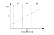
したがって、図7に示すように、右位相差画素42aの比感度(通常画素43の感度に対する感度)は、概ねX方向の位置に比例し、右周辺部11bRでは中央部11aのものよりも大きいが、左周辺部11bLでは中央部11aのものよりも小さい。このため、比感度が大きい右周辺部11bRの右位相差画素42aを用いる場合には、中央部11aのものを用いる場合よりも精度良く位相差AFを行うことができる。しかし、比感度が中央部11aのものよりも小さい左周辺部11bLの右位相差画素42aを用いると、位相差AFの精度が良好ではない。
図8及び図9に示すように、受光領域11の中心(中央部11aの中心線)から左周辺部11bLにある右位相差画素42aの開口56Rを、中心部11a及び右周辺部11bRの開口56Rよりも、面積を大きくしてある。このように、開口面積を中央部11a及び右周辺部11bRのものよりも大きくすると、左周辺部11bLにある右位相差画素42aの感度を、中央部11aにある右位相差画素42aの感度以上に向上させることができる。
例えば、開口面積が、図6に示す中央部11aのものと同じ場合に、一部が遮光されていた左側光束(実線矢印)が、図8に示すように開口面積を拡大した場合には、ほぼ全てがPD22に到達する。また、開口面積が中央部11aのものと同じ場合には、全て遮光されていた右側光束(破線矢印)は、面積が拡大された開口56Rを通過してPD22に到達する。このため、右側光束の約1/5がPD22に到達すると、面積が拡大された開口56Rを有する左周辺部11bLの位相差画素42aの受光量は、入射光量の約3/5程度に向上する。これは、右周辺部11bRにある右位相差画素42aの受光量とほぼ同じ受光量である。
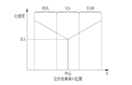
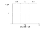
左周辺部11bLにおける開口56Rの拡大率は、例えば、図10に示すように、比感度が中央部11aの中心線から左周辺部11bLと、中心線から右周辺部11bRとで対称になるように、各右位相差画素42aの位置に応じて調節すればよい。なお、左周辺部11bLにおける開口56Rの拡大率は、左周辺部11bLにある右位相差画素42aの比感度が、少なくとも中央部11aの右位相差画素42aの比感度以上になるように調節されていればよい。特に、図11に示すように、受光領域11の中心から左周辺部11bLにかけて比感度が一定になるように、開口56Rの拡大率が調節されていることが好ましい。このように、受光領域11の中心における比感度と、左周辺部11bLの比感度とが等しくなるように開口56Rの拡大率が調節されている場合は、左周辺部11bLの右位相差画素42aが本来受光すべき左側光束(信号)が多く、ノイズになる右側光束の受光量が少ないので、良好なS/Nを維持したまま、比感度を大きくできる。
図12に示すように、右周辺部11bRにある右位相差画素42aの開口56Rは、中央部11aのものよりも小さくしてもよい。そして、右周辺部11bRにおける開口56Rの縮小率は、図13に示すように、受光領域11の中心から右周辺部11bRにかけて比感度が一定になるように調節されていることが好ましい。このように、受光領域11の中心における比感度と、右周辺部11bRの比感度とが等しくなるように開口56Rの面積が調節されている場合は、開口面積が中心のものと同じ場合と比較すれば比感度が低下するが、S/Nを向上させることができる。また、上述の説明から分かるように、図13のように、中央部11a,左周辺部11bL,右周辺部11bRで、比感度がほぼ等しくなるように開口56Rの面積が調節されていることが特に好ましいことは言うまでもない。
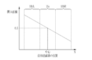
ところで、左位相差画素42bは、右位相差画素42aと断面構造が左右対称である。このため、図14に示すように、左位相差画素42bは、上述の右位相差画素42aの場合とは逆に、少なくとも受光領域11の中心から右周辺部11bRにかけて開口56Lの面積が大きくなるように開口面積が調節されている。
図15に示すように、左位相差画素42bの開口面積が一定になっている場合に、右周辺部11bR上の左位相差画素42bの比感度は、中央部11aのものよりも低い(一点鎖で示す)。しかし、右周辺部11bR上の左位相差画素42bの開口面積を拡大しておくことで、右周辺部11bR上の左位相差画素42bは、左周辺部11bL上の左位相差画素42bと同程度(実線で示す)に、あるいは中央部11aの中心と同程度(破線で示す)に、比感度が向上する。
右位相差画素42aの開口56Rは、左周辺部11bLで拡大し、右周辺部11bRでは中央部11aと同じか、あるいは縮小している。同様に、左位相差画素42bの開口56Lは、右周辺部11bRで拡大し、左周辺部11bLでは中央部11aと同じか、あるいは縮小している。このように、左右の位相差画素42a,42bは、位置に応じて開口面積を調節しているので、左右の位相差画素の感度を適切に補い、位相差AFの精度を向上することができる。
例えば、左右の位相差画素42a,42bを区別することなく、受光領域11の中心線からの距離に応じて、一律に開口面積を拡大すると、もともと比感度が大きい位置にある位相差画素(右周辺部11bR上の右位相差画素42aと、左周辺部11bL上の左位相差画素42b)では、ノイズになる光束の受光量が増えるので、S/Nが悪化し、比感度が高くても位相差AFの精度が悪化する場合がある。これと比較すると、左右の位相差画素42a,42bは、位置に応じて開口56L,56Rの大きさを調節しているので、S/Nを悪化させることなく、確実に位相差AFの精度を向上させることができる。
また、位相差画素42a,42bのマイクロレンズ75を通常画素43とは異なるスケーリングにすると、混色等が発生して撮影画像の画質が損なわれることもある。しかし、本実施形態では、マイクロレンズ75を通常画素43と異なったスケーリングをせずに、位相差画素42a,42bの開口面積の調節によって、位相差AFの精度を向上させているので、撮影画像の画質は損なわれない。
右位相差画素42aの開口面積を上述のように調節する場合に、例えば、図16に示すように、左周辺部11bLでは、中央部11aの右位相差画素42aの開口56Rに対して、右位相差画素42aの左端の位置を左側に移動して開口56Rの横に拡張することによって、面積を拡大すればよい。このように、中央部11aの右位相差画素42aの開口56Rに対して、右端の位置を揃えたまま開口を横に拡張して、面積を拡大すると、S/Nと比感度の向上を両立させやすい。この場合に、開口面積を拡大しても基線長(一対の位相差画素42a,42bの中心間の距離)が短くなり難いので、視差に関する情報も得やすい。図16では右位相差画素42aを例にしているが、左位相差画素42bも同様であり、右周辺部11bRにおいて、左端の位置を中央部11aのものと揃えたまま、右端の位置を右側に移動して開口56Lを横に拡張することによって面積を拡大すればよい。
一方、図17に示すように、左周辺部11bLの右位相差画素42aでは、中央部11aの右位相差画素42aの開口56Rの右端及び左端を両方とも左側に移動させて開口面積を拡大してもよい。この場合に、開口56Rの中心位置も左側に移動する。このように、開口面積の拡大のために、開口56Rの右端及び左端の位置をともに左側に移動させると、開口56Rの幅をできるだけ小さく保った状態で、左側光束をほぼ全て受光した場合でも、ノイズになる右側光束の入射を防ぐように開口面積を拡大することができる。このため、前述の右端を移動させない場合と比較すると、比感度の増分が少なく、また、基線長も短くなりやすいが、S/Nが特に良好である。なお、左位相差画素42bも左位相差画素42bと同様である。
左周辺部11bLの右位相差画素42aの開口面積を調節した上で、さらに図18に示すように、左周辺部11bLの右位相差画素42aのPD22を中央部11aのPD22に対して小さくしてもよい。左周辺部11bLの右位相差画素42aのPD22を小さくすると、右位相差画素42aのPD22は、その横にある通常画素43のPD22からの距離が大きくなる。通常画素43のPD22と右位相差画素42aのPD22の距離が近い場合に、通常画素43に斜めに入射した光が右位相差画素42aのPD22に漏れ、混色が発生する場合がある。しかし、上述のように、右位相差画素42aのPD22を小さくしておけば、通常画素43に斜めに入射した光が位相差画素42a側に漏れても、右位相差画素42aのPD22には到達し難いので、混色がより確実に防止され、S/Nが良い信号が得られやすい。
左周辺部11bLの右位相差画素42aのPD22を小さくする場合は、開口56Rの面積や、PD22の大きさ及び形状は、比感度及びS/Nが最適になるように適宜定めればよい。また、PD22の大きさ及び形状を、拡大した右位相差画素42aの開口56Rに合わせた長方形にしてもよい。例えば、右位相差画素42aの開口56Rに大きさや形状がほぼ合致する長方形にすればよい。なお、左位相差画素42bについても同様である。
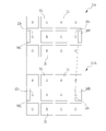
上述の実施形態では、受光領域を中央部11aと周辺部11bL,11bRの3つに区画しているが、受光領域11aをさらに細かく区分けしてもよい。例えば、図19に示すように、受光領域11を、左中央部81aL,右中央部81aR、内側左周辺部81bL,内側右周辺部81bR,外側左周辺部81cL,外側右周辺部81cRに分けてもよい。これらの内側左周辺部81bL,内側右周辺部81bR,外側左周辺部81cL,外側右周辺部81cRはチャンネル状をしているが、垂直方向に延びた矩形でもよい。撮影画像のシェーディング補正や傷補正(位相差画素42a,42bの画素値の補正)等の所定の各種処理の方法が受光領域11の位置によって異なる場合があるが、上述のように受光領域11を細かく区分けする場合には、各種処理の方法の区切りに合わせて受光領域11を区分けすることが好ましい。
さらに、図20に示すように、右位相差画素42aの開口面積を、左中央部81aL,内側左周辺部81bL,外側左周辺部81cLの順に段階的に拡大してもよい。このように、各種処理の方法が異なる区切りに合わせて、右位相差画素42aの開口面積を段階的に拡大すると、中心からの距離に応じて開口面積を滑らかに拡大する(図9参照)よりも容易に良好な処理結果が得られる。すなわち、右位相差画素42aの開口面積の段階的拡大は、位相差AFの精度向上と撮影画像の画質を両立しやすい。なお、右中央部81aR,内側右周辺部81bR,外側右周辺部81cRでは、右位相差画素42aの開口面積は同じである。また、左位相差画素42bは、右位相差画素42aと同様に、右中央部81aR,内側右周辺部81bR,外側右周辺部81cRで段階的に開口面積を拡大すればよい。なお、受光領域11を中央部11aと周辺部11bL,11bRに分ける場合も、開口面積を段階的に拡大してもよい。
撮像レンズ44がズームレンズの場合に、ズーム倍率によって各位置の主光線角度45が変化するので、各位置の位相差画素42a,42bの開口面積を一義的に定められない場合がある。この場合には、撮像レンズ44が望遠端(焦点距離が最も長い場合)、広角端(焦点距離が最も短い場合)、またはこれらの中間位置の場合に、無限遠距離からの主光線角度45に合わせて各位置の位相差画素42a,42bの開口面積を定めることが好ましい。但し、望遠端の場合の主光線角度45に合わせると広角端での誤差(比感度等のずれ)が大きく、逆に広角端の場合の主光線角度45に合わせると望遠端での誤差が大きい。そこで、望遠端と広角端とで位相差AFの精度を同じにするために、望遠端と広角端との中間位置での主光線角度45に合わせて、各位相差画素42a,42bの開口面積を定めることが特に好ましい。
上述の実施形態では、G画素を位相差画素42a,42bとしているが、図21に示すように、R画素やB画素を位相差画素42a,42bにしてもよい。もちろん、全ての位相差画素42a,42bをR画素で形成してもよいし、全ての位相差画素42a,42bをB画素で形成してもよい。また、R,G,Bのいずれか2種を位相差画素42a,42bとしてもよい。
但し、位相差画素42a,42bをR,G,Bのうち2色以上とする場合に、色毎に周辺部11bにおける感度の低下量が異なるので、色毎に位相差画素42a,42bの開口面積の拡大率を変えることが好ましい。マイクロレンズ75の焦点距離等によっても異なるが、例えば、各色の位相差画素42a,42bの開口面積の拡大率をB画素>G画素>R画素にする。もちろん、開口面積の拡大率が2色で同じであり、1色だけ異なっていてもよい(例えば、B画素=G画素>R画素)。拡大率の基準は、中央部11aにある各色の位相差画素42a,42bの開口面積である。このように、色毎に位相差画素42a,42bの開口面積の拡大率を調節しておけば、各色の位相差画素42a,42bでS/Nが良い信号が得られるので、位相差AFの精度を向上させやすい。
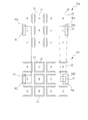
上述の実施形態では、固体撮像装置10の画素が正方配列されているが、画素の配列は任意である。例えば、画素の配列を図22及び図23のようにハニカム配列にしてもよい。また、画素配列をハニカム配列にする場合のカラーフィルタの色配列は任意であるが、例えば、図22や図23の色配列にすることができる。図22の色配列は、G画素の列と、R画素及びB画素が2個ずつ交互に並んだ列を斜め45度方向に交互に配置した例である。
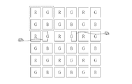
また、6×6画素を単位としたカラーフィルタ41を用いているが、カラーフィルタ41の配列は任意である。例えば、画素を正方配列にする場合には、図24に示すように、破線で囲む2×2画素を上下左右に並べたいわゆるベイヤー配列にしてもよい。
位相差画素42a,42bは、カラーフィルタ41の6×6画素の単位内で、右上の第1サブユニット41aの左下G画素と、左上の第2サブユニット41bの左下G画素に形成しているが、位相差画素42a,42bを形成するG画素の位置は任意である。例えば、右上の第1サブユニット41aの中央のG画素と、左上の第2サブユニット41bの中央のG画素をそれぞれ位相差画素42a,42bとしてもよい。また、右下の第2サブユニット41bのG画素と、左下の第1サブユニット41aのG画素を位相差画素42a,42bとしてもよい。
また、一対の位相差画素42a,42bは、同じ行内に設けられているが、これらを異なる行に設けてもよい。
位相差画素42a,42bは、X方向(水平方向)に非対称に形成され、位相差画素42a,42bが左右(水平方向)の視差を取得しているが、Y方向(上下方向)や斜め方向の視差情報を取得してもよい。例えば、位相差画素の構造(開口の位置)を縦方向に非対称にし、対になる位相差画素を上下に並べて、上下方向の視差を得てもよい。また、斜め方向の視差を得る場合には、同様に斜め方向に非対称な構造の位相差画素の対を斜め方向に配置すればよい。
更に、X方向の視差を得る位相差画素42a,42b、Y方向の視差を得る位相差画素、斜め方向の視差を得る位相差画素の3種類のうち、2種類以上を受光領域11に設けておいてもよい。X方向の視差を得る位相差画素や斜め方向の視差を得る位相差画素を設ける場合は、これらの各方向の位相差画素も、上述の実施形態の左右の位相差画素42a,42bと同様に、受光する光束の方向と、受光領域11内の位置に応じて、開口を拡大することが好ましい。
なお、複数の位相差画素42a,42bは、受光領域11内に均一に配置されているが、位相差画素42a,42bの個数や配置及び分布は任意である。
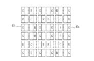
上述の実施形態及び変形例では、受光領域11内の一部に位相差画素42a,42bが配置されているが、図25に示すように、全画素を位相差画素42a,42bにしてもよい。全画素を位相差画素42a,42bにすると、例えば、単眼(1個の固体撮像装置)で3D画像を得ることができる。図25では、画素が正方配列であるが、画素をハニカム配列にしてもよい。また、カラーフィルタはベイヤー配列でもよい。
1つの画素には、3個のトランジスタTr23,Ta24,Ts25が用いられているが、入射光を各々光電変換し、撮影画像の形成や位相差AFに必要な画素信号を出力することができれば、トランジスタの数等は任意である。例えば、PD22とFDの間に転送用のトランジスタを追加してもよい。
遮光層54とカラーフィルタ41とは積層されているが、遮光層54の開口55,56内にカラーフィルタ41の各色セグメントを埋め込むことで、遮光層54とカラーフィルタ41を一体に形成してもよい。
また、p型半導体基板53の裏面に、遮光層54、カラーフィルタ41が順に積層されているが、遮光層54とカラーフィルタ41の積層順は逆順でもよい。
カラーフィルタは、原色系のカラーフィルタ41の他に、補色系のカラーフィルタを用いてもよい。なお、本明細書のカラーフィルタにはNDフィルタが含まれるものとし、位相差画素42a,42にはこのNDフィルタを設けてもよい。
また、遮光層54の開口55,56に透明な材料を充填して遮光層54を平坦化しているが、開口55,56にはカラーフィルタ41の材料が充填されていてもよい。
遮光層54内では、通常画素43間にも遮光材料が設けられ、各通常画素43の開口55が分離しているが、通常画素43間の遮光材料を設けず、通常画素43の開口55の全てを連続させてもよい。この場合に、遮光層54は、位相差画素42a,42bにおいて入射光を制限する部分にだけ遮光材料を配置したものになる。
上述の実施形態及び変形例では、固体撮像装置10がCMOS型イメージセンサであるが、CCD型イメージセンサでもよい。
また、固体撮像装置10は、裏面照射型のイメージセンサであるが、表面照射型(FSI;front side illuminated)のイメージセンサでもよい。この表面照射型イメージセンサでは、配線層を介してPDに光が入射する。
本発明の固体撮像装置は、薄型のデジタルカメラ、携帯電話機やPDA、スマーフォトン等に搭載されるカメラモジュールに好適である。特に、バックフォーカスの短い撮像レンズ44と、受光領域が広い固体撮像装置の組合せにより、周辺部で主光線角度が大きいカメラやカメラモジュールに好適である。
10 固体撮像装置
11 受光領域
11a 中央部
11bL 左周辺部
11bR 右周辺部
21 画素
42a 右位相差画素
42b 左位相差画素
43 通常画素
55,56L,56R 開口
11 受光領域
11a 中央部
11bL 左周辺部
11bR 右周辺部
21 画素
42a 右位相差画素
42b 左位相差画素
43 通常画素
55,56L,56R 開口
Claims (10)
- 被写体の像が形成される受光領域に配置され、入射光を等方的に受光する複数の通常画素と、
前記受光領域内に配置されており、第1方向に偏心配置された第1開口を有し、この第1開口を通って、前記第1方向での下流側に到達した光を選択的に受光する複数の第1位相差画素と、
前記受光領域内に配置されており、前記第1方向とは逆の第2方向に偏心配置された第2開口を有し、この第2開口を通って、前記第2方向での下流側に到達した光を選択的に受光する複数の第2位相差画素とを備え、
前記受光領域のうち前記第1方向での下流側にある周辺部を第1周辺部とし、上流側にある周辺部を第2周辺部とし、前記第1周辺部と前記第2周辺部との間を中央部とすると、前記第2周辺部に存在する前記第1位相差画素は、前記中央部及び前記第1周辺部に存在する前記第1位相差画素に対して、前記第1開口の面積を大きくし、
前記第1周辺部に存在する前記第2位相差画素は、前記中央部及び前記第2周辺部に存在する前記第2位相差画素に対して、前記第2開口の面積を大きくしている固体撮像装置。 - 前記第2周辺部に存在する前記第1位相差画素の前記第1開口は、前記中央部に存在する前記第1位相差画素の前記第1開口に対して、前記第2方向に拡張され、
前記第1周辺部に存在する前記第2位相差画素の前記第2開口は、前記中央部に存在する前記第2位相差画素の前記第2開口に対して、前記第1方向に拡張されている請求項1に記載の固体撮像装置。 - 前記第2周辺部に存在する前記第1位相差画素の前記第1開口の中心位置は、前記中央部に存在する前記第1位相差画素の前記第1開口に対して、前記第2方向に寄り、
前記第1周辺部に存在する前記第2位相差画素の前記第2開口の中心位置は、前記中央部に存在する前記第2位相差画素の前記第2開口に対して、前記第1方向に寄っている請求項1に記載の固体撮像装置。 - 前記第2周辺部に存在する前記第1位相差画素及び前記第1周辺部に存在する前記第2位相差画素のフォトダイオードは、前記中央部に存在する前記第1位相差画素及び前記第2位相差画素のフォトダイオードよりも受光面積が小さい請求項1に記載の固体撮像装置。
- 前記第1開口の面積は、前記中央部から前記第2周辺部に向かって拡大され、
前記第2開口の面積は、前記中央部から前記第1周辺部に向かって拡大されている請求項1に記載の固体撮像装置。 - 前記第1及び第2位相差画素は、3原色の色光を光電変換するために、各色光に対応して3種類があり、
前記中央部から前記第2周辺部に向かって拡大される前記第1開口の拡大率と、前記中央部から前記第1周辺部に向かって拡大される前記第2開口の拡大率は、光電変換すべき前記色光の種類に応じて決められている請求項1に記載の固体撮像装置。 - 前記固体撮像装置の前に配置されるズームレンズが望遠端と広角端との中間位置にセットされたときに、無限遠からの被写体光がズームレンズを出射するときの出射角度に基づいて、前記第2周辺部に存在する前記第1位相差画素の前記第1開口と、前記第1周辺部に存在する前記第2位相差画素の前記第2開口の面積がそれぞれ定められている請求項1に記載の固体撮像装置。
- 前記第1周辺部に存在する前記第1位相差画素は、前記中央部に存在する前記第1位相差画素に対して、前記第1開口が小さく、
前記第2周辺部に存在する前記第2位相差画素は、前記中央部に存在する前記第2位相差画素に対して、前記第2開口が小さい請求項1に記載の固体撮像装置。 - 前記通常画素、前記第1位相差画素、及び前記第2位相差画素は、前記入射光を集光するマイクロレンズを有し、
前記第1及び第2周辺部に存在する前記通常画素、前記第1位相差画素、及び前記第2位相差画素は、前記入射光の入射角度に応じて、前記中央部に向かって偏心して配置されている請求項1に記載の固体撮像装置。 - 第1方向に偏心配置された第1開口を有し、前記入射光のうち前記第1方向での側部に到達した光を、前記第1開口を通して選択的に受光する複数の第1位相差画素と、
前記第1方向とは逆の第2方向に偏心配置された第2開口を有し、前記入射光のうち前記第2方向での側部に到達した光を、前記第2開口を通して選択的に受光する第2位相差画素と、
前記第1及び第2位相差画素だけが、被写体の像が形成される受光領域に配置されている固体撮像装置であって、
前記受光領域のうち前記第1方向での下流側にある周辺部を第1周辺部とし、上流側にある周辺部を第2周辺部とし、前記第1周辺部と前記第2周辺部との間を中央部とすると、前記第2周辺部に存在する前記第1位相差画素は、前記中央部及び前記第1周辺部に存在する前記第1位相差画素とに対して、前記第1開口の面積を大きくし、
前記第1周辺部に存在する前記第2位相差画素は、前記中央部及び前記第2周辺部に存在する前記第2位相差画素に対して、前記第2開口の面積を大きくしている固体撮像装置。
Applications Claiming Priority (2)
| Application Number | Priority Date | Filing Date | Title |
|---|---|---|---|
| JP2012-275453 | 2012-12-18 | ||
| JP2012275453A JP2016029674A (ja) | 2012-12-18 | 2012-12-18 | 固体撮像装置 |
Publications (1)
| Publication Number | Publication Date |
|---|---|
| WO2014097884A1 true WO2014097884A1 (ja) | 2014-06-26 |
Family
ID=50978219
Family Applications (1)
| Application Number | Title | Priority Date | Filing Date |
|---|---|---|---|
| PCT/JP2013/082558 Ceased WO2014097884A1 (ja) | 2012-12-18 | 2013-12-04 | 固体撮像装置 |
Country Status (2)
| Country | Link |
|---|---|
| JP (1) | JP2016029674A (ja) |
| WO (1) | WO2014097884A1 (ja) |
Cited By (3)
| Publication number | Priority date | Publication date | Assignee | Title |
|---|---|---|---|---|
| JP2016031498A (ja) * | 2014-07-30 | 2016-03-07 | 株式会社ニコン | 撮像素子および撮像装置 |
| WO2020012860A1 (ja) * | 2018-07-09 | 2020-01-16 | ソニーセミコンダクタソリューションズ株式会社 | 撮像素子および撮像素子の製造方法 |
| US20210306581A1 (en) * | 2016-06-28 | 2021-09-30 | Sony Group Corporation | Solid-state imaging device, electronic apparatus, lens control method, and vehicle |
Families Citing this family (6)
| Publication number | Priority date | Publication date | Assignee | Title |
|---|---|---|---|---|
| JP2018056522A (ja) * | 2016-09-30 | 2018-04-05 | 株式会社ニコン | 撮像素子および焦点調節装置 |
| KR102375989B1 (ko) | 2017-08-10 | 2022-03-18 | 삼성전자주식회사 | 화소 사이의 신호 차이를 보상하는 이미지 센서 |
| KR102549481B1 (ko) * | 2018-05-10 | 2023-06-30 | 에스케이하이닉스 주식회사 | 이미지 센싱 장치 |
| CN110086972A (zh) * | 2019-04-28 | 2019-08-02 | 深圳市超诺科技有限公司 | 一种摄像头智能补光系统 |
| JP7381067B2 (ja) * | 2019-11-19 | 2023-11-15 | 株式会社シグマ | 撮像素子及び撮像装置 |
| JP7699566B2 (ja) * | 2022-09-16 | 2025-06-27 | キヤノン株式会社 | 撮像装置及びその制御方法及びプログラム |
Citations (4)
| Publication number | Priority date | Publication date | Assignee | Title |
|---|---|---|---|---|
| JP2004172836A (ja) * | 2002-11-19 | 2004-06-17 | Canon Inc | 画像読み取り装置 |
| JP2005117008A (ja) * | 2003-09-19 | 2005-04-28 | Fuji Film Microdevices Co Ltd | 固体撮像素子 |
| JP2010278664A (ja) * | 2009-05-27 | 2010-12-09 | Sony Corp | 固体撮像素子及び撮像装置 |
| JP2012182332A (ja) * | 2011-03-02 | 2012-09-20 | Sony Corp | 撮像素子および撮像装置 |
-
2012
- 2012-12-18 JP JP2012275453A patent/JP2016029674A/ja active Pending
-
2013
- 2013-12-04 WO PCT/JP2013/082558 patent/WO2014097884A1/ja not_active Ceased
Patent Citations (4)
| Publication number | Priority date | Publication date | Assignee | Title |
|---|---|---|---|---|
| JP2004172836A (ja) * | 2002-11-19 | 2004-06-17 | Canon Inc | 画像読み取り装置 |
| JP2005117008A (ja) * | 2003-09-19 | 2005-04-28 | Fuji Film Microdevices Co Ltd | 固体撮像素子 |
| JP2010278664A (ja) * | 2009-05-27 | 2010-12-09 | Sony Corp | 固体撮像素子及び撮像装置 |
| JP2012182332A (ja) * | 2011-03-02 | 2012-09-20 | Sony Corp | 撮像素子および撮像装置 |
Cited By (10)
| Publication number | Priority date | Publication date | Assignee | Title |
|---|---|---|---|---|
| JP2016031498A (ja) * | 2014-07-30 | 2016-03-07 | 株式会社ニコン | 撮像素子および撮像装置 |
| US20210306581A1 (en) * | 2016-06-28 | 2021-09-30 | Sony Group Corporation | Solid-state imaging device, electronic apparatus, lens control method, and vehicle |
| WO2020012860A1 (ja) * | 2018-07-09 | 2020-01-16 | ソニーセミコンダクタソリューションズ株式会社 | 撮像素子および撮像素子の製造方法 |
| CN112368837A (zh) * | 2018-07-09 | 2021-02-12 | 索尼半导体解决方案公司 | 摄像元件和摄像元件的制造方法 |
| US11477403B2 (en) | 2018-07-09 | 2022-10-18 | Sony Semiconductor Solutions Corporation | Imaging element and method for manufacturing imaging element |
| CN115767295A (zh) * | 2018-07-09 | 2023-03-07 | 索尼半导体解决方案公司 | 光检测装置和相机 |
| CN115767295B (zh) * | 2018-07-09 | 2023-09-15 | 索尼半导体解决方案公司 | 摄像元件和相机 |
| US11765476B2 (en) | 2018-07-09 | 2023-09-19 | Sony Semiconductor Solutions Corporation | Imaging element and method for manufacturing imaging element |
| US12022217B2 (en) | 2018-07-09 | 2024-06-25 | Sony Semiconductor Solutions Corporation | Imaging element and method for manufacturing imaging element |
| CN112368837B (zh) * | 2018-07-09 | 2024-11-15 | 索尼半导体解决方案公司 | 摄像元件和摄像元件的制造方法 |
Also Published As
| Publication number | Publication date |
|---|---|
| JP2016029674A (ja) | 2016-03-03 |
Similar Documents
| Publication | Publication Date | Title |
|---|---|---|
| US11444115B2 (en) | Solid-state imaging device and electronic apparatus | |
| JP5860168B2 (ja) | 固体撮像装置 | |
| WO2014097884A1 (ja) | 固体撮像装置 | |
| US10594961B2 (en) | Generation of pixel signal with a high dynamic range and generation of phase difference information | |
| JP5422889B2 (ja) | 固体撮像素子及びこれを用いた撮像装置 | |
| CN102693989B (zh) | 固体摄像装置、固体摄像装置的制造方法以及电子设备 | |
| CN105308748B (zh) | 固态成像装置和电子设备 | |
| JP5157436B2 (ja) | 固体撮像素子および撮像装置 | |
| US20180077372A1 (en) | Solid-state imaging element and driving method therefor, and electronic apparatus | |
| JP5045012B2 (ja) | 固体撮像素子及びこれを用いた撮像装置 | |
| JP2020077886A (ja) | 撮像素子 | |
| US20150163464A1 (en) | Solid-state imaging device | |
| JP5629995B2 (ja) | 撮像素子および撮像装置 | |
| CN114695413A (zh) | 光检测器件和电子设备 | |
| JP2016052041A (ja) | 固体撮像素子及びその信号処理方法、並びに電子機器 | |
| JP2015115345A (ja) | 固体撮像装置 | |
| JP4839990B2 (ja) | 固体撮像素子及びこれを用いた撮像装置 | |
| KR20140137951A (ko) | 위상차 초점검출 가능한 촬상소자 | |
| JP2016139660A (ja) | 固体撮像装置 | |
| JP2014003116A (ja) | 撮像素子 | |
| JP2012004264A (ja) | 固体撮像素子および撮影装置 |
Legal Events
| Date | Code | Title | Description |
|---|---|---|---|
| 121 | Ep: the epo has been informed by wipo that ep was designated in this application |
Ref document number: 13865120 Country of ref document: EP Kind code of ref document: A1 |
|
| NENP | Non-entry into the national phase |
Ref country code: DE |
|
| 122 | Ep: pct application non-entry in european phase |
Ref document number: 13865120 Country of ref document: EP Kind code of ref document: A1 |
|
| NENP | Non-entry into the national phase |
Ref country code: JP |