WO2014097673A1 - トランス - Google Patents
トランス Download PDFInfo
- Publication number
- WO2014097673A1 WO2014097673A1 PCT/JP2013/070730 JP2013070730W WO2014097673A1 WO 2014097673 A1 WO2014097673 A1 WO 2014097673A1 JP 2013070730 W JP2013070730 W JP 2013070730W WO 2014097673 A1 WO2014097673 A1 WO 2014097673A1
- Authority
- WO
- WIPO (PCT)
- Prior art keywords
- coil pattern
- primary
- surface shape
- coil
- insulating layer
- Prior art date
- Legal status (The legal status is an assumption and is not a legal conclusion. Google has not performed a legal analysis and makes no representation as to the accuracy of the status listed.)
- Ceased
Links
Images



Classifications
-
- H—ELECTRICITY
- H01—ELECTRIC ELEMENTS
- H01F—MAGNETS; INDUCTANCES; TRANSFORMERS; SELECTION OF MATERIALS FOR THEIR MAGNETIC PROPERTIES
- H01F27/00—Details of transformers or inductances, in general
- H01F27/28—Coils; Windings; Conductive connections
- H01F27/2847—Sheets; Strips
-
- H—ELECTRICITY
- H01—ELECTRIC ELEMENTS
- H01F—MAGNETS; INDUCTANCES; TRANSFORMERS; SELECTION OF MATERIALS FOR THEIR MAGNETIC PROPERTIES
- H01F27/00—Details of transformers or inductances, in general
- H01F27/28—Coils; Windings; Conductive connections
- H01F27/2847—Sheets; Strips
- H01F2027/2857—Coil formed from wound foil conductor
Definitions
- the present invention relates to a transformer having a coil pattern having a surface shape.
- FIG. 4 is a cross-sectional view of a prior art transformer. Each of the primary winding 101 and the secondary winding 102 shown in FIG. 4 is covered with an insulating member.
- the current flowing in the primary winding 101 or the secondary winding is caused by a so-called proximity effect in the mode shown in FIG.
- the currents flowing in the wire 102 repel each other, and the currents flowing in the windings 101 and 102 flow at positions separated from each other.
- the cross-sectional area through which the current flows in the windings 101 and 102 becomes small, and as a result, the resistance increases.
- the primary winding 101 or secondary located inside is affected by both the skin effect and the proximity effect. It becomes difficult for current to flow through the winding 102, and the resistance increases considerably. More specifically, in the aspect shown in FIG. 4, the primary winding 101 in the second row of the primary windings 101 in the three rows and the primary winding 101 not located at the upper and lower ends and the two rows in the three rows. Of the secondary windings 102, the secondary windings 102 in the second row and the secondary windings 102 that are not positioned at the upper and lower ends make it difficult for current to flow, and the resistance increases considerably.
- JP-A-7-130554 is known in addition to the above-mentioned JP-A-2012-164928.
- JP-A-7-130554 a first conductive film body obtained by printing a thin strip-shaped conductor layer in a stripe shape and a second conductive film body obtained by printing a thick strip-shaped conductor layer in a stripe shape. Is disclosed.
- thin strip conductor layers are adjacent to each other on the same plane, and thick strip conductor layers are adjacent to each other on the same plane. And since the current flows in the same direction in the strip conductor layers adjacent to each other, due to the proximity effect described above, the currents flowing in the thin strip conductor layer and the currents flowing in the thick strip conductor layer repel each other, In each strip conductor layer, the cross-sectional area through which current flows becomes small.
- the present invention prevents the current flowing region from being reduced by the skin effect even when operated at a high frequency, and the cross sectional area through which the current flows is reduced by the proximity effect.
- a transformer that can efficiently pass a current can be reduced in size, and can be prevented from collapsing is provided.
- the transformer according to the present invention is It has a coil part that is wound into a pillar shape,
- the coil portion is A plurality of primary coil patterns having a primary surface shape portion composed of a single surface shape;
- the insulating layer and the secondary coil pattern are in intimate contact,
- Each primary surface shape portion occupies one region in the direction orthogonal to the winding direction of the coil portion, and occupies a different region in the winding direction of the coil portion
- the secondary surface shape portion occupies one region in a direction perpendicular to the winding direction of the coil portion,
- the number of times the secondary coil pattern is wound is greater than the number of times the primary coil pattern is wound.
- the ratio of the number of times the secondary coil pattern is wound to the number of times the primary coil pattern is wound may be n: 1 (“n” is an integer of 2 or more).
- the primary coil pattern and the secondary coil pattern are viewed along the radial direction of the coil portion, the primary coil pattern, the order of the secondary coil pattern or the secondary coil pattern, the primary coil pattern They may be arranged in order.
- the insulating layer has an insulating film disposed between the primary coil pattern and the secondary coil pattern,
- the primary coil pattern is provided on one surface of the insulating film,
- the secondary coil pattern may be provided on the other surface of the insulating film.
- the insulating layer may include a primary insulating layer formed so as to cover the primary coil pattern or a secondary insulating layer formed so as to cover the secondary coil pattern.
- the insulating layer may include a primary insulating layer formed so as to cover the primary coil pattern and a secondary insulating layer formed so as to cover the secondary coil pattern.
- the primary coil pattern has a primary protruding portion that protrudes in a direction including a component in a direction orthogonal to the winding direction of the coil portion from the primary surface shape portion
- the secondary coil pattern has a secondary protrusion protruding in a direction including a component in a direction orthogonal to the winding direction of the coil part from the secondary surface shape part
- the direction in which the primary protrusion protrudes from the primary surface shape portion and the direction in which the secondary protrusion protrudes from the secondary surface shape portion may have components opposite to each other.
- a heat radiating member made of an insulating material may be provided at a position on the direction side perpendicular to the winding direction of the coil portion with respect to the primary surface shape portion and adjacent to the primary surface shape portion.
- a heat dissipating member made of an insulating material may be provided at a position on the direction side perpendicular to the winding direction of the coil portion with respect to the secondary surface shape portion and adjacent to the secondary surface shape portion.
- the coil portion further includes a tertiary coil pattern having a tertiary surface shape portion composed of a single-layer surface shape,
- the tertiary surface shape portion occupies one region in a direction orthogonal to the winding direction of the coil portion, The number of times that the tertiary coil pattern is wound is greater than the number of times that the secondary coil pattern is wound,
- the primary coil pattern, the secondary coil pattern, and the tertiary coil pattern are viewed along the radial direction of the coil portion, the order of the primary coil pattern, the secondary coil pattern, the tertiary coil pattern, or the You may arrange
- the transformer according to the present invention is It further includes a core having a columnar portion made of a columnar shape, The coil part may be wound around the columnar part.
- the transformer according to the present invention is You may further provide the cooling storage part which stored the antifreeze liquid in which the said coil part is immersed.
- a primary coil pattern having a primary surface shape portion having a single layer shape and a secondary coil pattern having a secondary surface shape portion having a single layer shape are employed. For this reason, even if it is a case where it operates at a high frequency, it can prevent that the area
- each primary surface shape portion occupies one region in a direction orthogonal to the winding direction of the coil portion (only one is provided), and similarly, the secondary surface shape portion is orthogonal to the winding direction of the coil portion. Occupying one region in the direction of the movement (only one is provided), the cross-sectional area of each primary surface shape portion and secondary surface shape portion can be increased, resulting in a high frequency (for example, Even when operating at 70 kHz), the influence of the skin effect can be kept small.
- the primary coil patterns and the secondary coil patterns when viewed along the radial direction, do not adjoin each other. It can suppress becoming small.
- this invention can prevent that resistance becomes large by limiting the area
- the size of the transformer can be reduced.
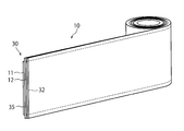
- the transformer 100 includes a core having a base portion, a columnar portion having a column shape extending from the base portion, and a coil portion 10 wound around the columnar portion and having a columnar shape. .
- description will be made using an embodiment provided with such a core, but it is sufficient that the coil portion 10 is wound in a columnar shape, and the core is not necessarily required.
- the coil portion 10 includes a plurality of primary coil patterns 11 (“3” in FIG. 3A) having a primary surface shape portion 11 a (see FIG. 3A) having a single-layer surface shape, and a single-layer surface shape.
- a secondary coil pattern 12 having a secondary surface shape portion 12a (see FIG. 3B), and an insulating layer 30 disposed between the primary coil pattern 11 and the secondary coil pattern 12.
- each primary surface shape part 11a occupies one area
- the secondary surface shape portion 12a occupies one region in a direction orthogonal to the winding direction of the coil portion 10 (vertical direction in FIG. 3B). In the present embodiment, since only one secondary surface shape portion 12a is provided, the secondary surface shape portion 12a is 1 in the winding direction of the coil portion (the left-right direction in FIG. 3B). Will occupy one area.
- the direction orthogonal to the winding direction of the coil part 10 is a direction where the axis
- the primary coil pattern 11 and the insulating layer 30 are in close contact, and the insulating layer 30 and the secondary coil pattern 12 are in close contact.
- the primary coil pattern 11 and the secondary coil pattern 12 are the order of the primary coil pattern 11 and the secondary coil pattern 12 or the secondary coil pattern 12.
- the primary coil patterns 11 are arranged in this order.
- the insulating layer 30 includes both the primary insulating layer 31 formed so as to cover the primary coil pattern 11 and the secondary insulating layer 32 formed so as to cover the secondary coil pattern 12.
- the coil part 10 has the tertiary coil pattern which has the tertiary surface shape part which consists of a single-layer surface shape, and the quaternary surface shape part which consists of a single-surface shape other than the primary coil pattern 11 and the secondary coil pattern 12.
- a quaternary coil pattern may have an l-order coil pattern having a l-order surface shape portion composed of a single-layer surface shape (“l” is an integer of 3 or more).
- the coil part 10 has the primary coil pattern 11, the secondary coil pattern 12, and the tertiary coil pattern
- the primary coil pattern 11 when it sees along the radial direction of the coil part 10, the primary coil pattern 11, the secondary coil pattern 12
- the tertiary coil pattern is arranged in the order of the primary coil pattern 11, the secondary coil pattern 12, and the tertiary coil pattern.
- a secondary coil When the primary coil pattern 11, the secondary coil pattern 12, and the tertiary coil pattern are seen along the radial direction of the coil part 10, a tertiary coil pattern, a secondary coil
- the pattern 12 and the primary coil pattern 11 may be arranged in this order.
- the coil unit 10 includes the primary coil pattern 11 and the secondary coil pattern 12
- the primary coil pattern 11 is provided on the insulating film 38
- the secondary coil pattern 12 is provided on another insulating film 39.
- a mode in which the primary coil pattern 11, the insulating film 38, the secondary coil pattern 12, and the insulating film 39 are arranged in this order can be used (see FIG. 1).
- FIG. 2A is a perspective view schematically showing the transformer 100 according to the second aspect of the embodiment of the present invention
- FIG. 2B is a diagram of the transformer 100 according to the second aspect of the embodiment of the present invention. It is a perspective view.
- the primary insulating layer 31 and a heat radiating member 40 described later are omitted in order to simply show the configuration of the transformer 100.
- FIG. 3A is a plan view showing the primary coil pattern 11 side by unfolding the coil portion 10 of the transformer 100 according to the second aspect of the present embodiment, and FIG. It is the top view which expand
- each primary coil pattern 11 is in the winding direction of the coil portion 10 (left and right direction in FIG. 3A).
- a mode in which different regions (three different regions in the mode shown in FIG. 3A) are occupied and only one secondary coil pattern 12 is provided can be used (see FIG. 3B).
- this aspect is an example to the last, and is not limited to the said aspect.
- n 1 (“n” is an integer of 2 or more).
- the ratio of the number of times the secondary coil pattern 12 is wound around the columnar portion to the number of times each primary coil pattern 11 is wound around the columnar portion is 3: It is 1. More specifically, as shown in FIGS. 3A and 3B, three primary coil patterns 11 are formed on the surface side of the insulating film 35 of the coil portion 10. On the other hand, one secondary coil pattern 12 is formed on the back side of the insulating film 35 of the coil portion 10. In the present embodiment, each primary coil pattern 11 of the coil portion 10 is wound so as to rotate once around the columnar portion, and the secondary coil pattern 12 of the coil portion 10 is wound around three times around the columnar portion. It is.
- the insulating layer 30 is not limited to the aspect having both the primary insulating layer 31 and the secondary insulating layer 32, and the insulating layer 30 has only the primary insulating layer 31 or only the secondary insulating layer 32. It may be.
- the insulating layer 30 has only the primary insulating layer 31, the outermost secondary coil pattern 12 is covered with the end insulating layer, and the insulating layer 30 has only the secondary insulating layer 32. In this case, the innermost primary coil pattern 11 is covered with the end insulating layer.
- each of the primary insulating layer 31, the secondary insulating layer 32, the insulating film 35, the end insulating layer and the separation insulating layer may be made of the same material or different materials. May be.
- a polyimide film can be given as an example of what is used for the primary insulating layer 31, the secondary insulating layer 32, the insulating film 35, the end insulating layer, and the insulating layer for separation.
- the primary coil pattern 11 protrudes from the primary surface shape portion 11a in a direction including a component perpendicular to the winding direction of the coil portion 10 (vertical direction in FIG. 3A), so-called “lead wire”.
- the secondary coil pattern 12 includes a component in a direction (vertical direction in FIG. 3B) perpendicular to the winding direction of the coil part 10 from the secondary surface shape part 12a. It may have a secondary protrusion that protrudes in the direction and also serves as a “lead line”. Then, the direction in which the primary protrusion protrudes from the primary surface shape portion 11a (for example, the direction toward the upper side of FIG. 3A) and the direction in which the secondary protrusion protrudes from the secondary surface shape portion 12a (for example, FIG. 3). (B) may have components opposite to each other.
- Each of the primary protrusion and the secondary protrusion has a cross-sectional area that matches the capacity of the primary coil pattern 11 and the secondary coil pattern 12.
- the cross-sectional areas of the primary protrusion and the secondary protrusion are slightly smaller than the cross-sectional areas of the primary coil pattern 11 and the secondary coil pattern 12. Even if it is such an aspect, since a primary protrusion part and a secondary protrusion part are each exposed outside and are easy to cool, it is hard to produce a trouble at the time of flowing an electric current.
- the position on the direction side perpendicular to the winding direction of the coil portion 10 with respect to the primary surface shape portion 11a and adjacent to the primary surface shape portion 11a (this embodiment In the embodiment, the heat dissipating member 40 made of an insulating material is provided on both the upper and lower sides of the primary surface shape portion 11a.
- the position on the direction side perpendicular to the winding direction of the coil portion 10 with respect to the secondary surface shape portion 12a and the position adjacent to the secondary surface shape portion 12a (in this embodiment, the shape of the secondary surface)
- a heat radiating member 40 made of an insulating material is provided on both the upper and lower sides of the portion 12a.
- the heat radiating member 40 is made of, for example, ceramic, sapphire, diamond, or the like.
- a plurality (“3" in FIG. 3) of primary coil patterns 11 having a primary surface shape portion 11a having a single surface shape and a secondary surface shape having a single surface shape.
- a secondary coil pattern 12 having a portion 12a is employed (see FIGS. 3A and 3B).
- Each primary surface shape portion 11a occupies one region in a direction (vertical direction in FIG. 3A) orthogonal to the winding direction of the coil portion 10, and similarly, the secondary surface shape portion 12a includes a coil portion.
- One region occupies a direction perpendicular to the winding direction of 10 (vertical direction in FIG. 3A).
- the width of the primary surface shape portion 11a can be increased as much as possible.
- the cross-sectional area of the surface-shaped part 11a can be increased as much as possible. For this reason, even when the skin effect occurs, the influence of the skin effect can be kept small, and the region through which the current flows can be made large in the primary surface shape portion 11a.
- the width of the secondary surface shape portion 12a can be increased as much as possible. It is possible to increase the cross-sectional area of the secondary surface shape portion 12a as much as possible. For this reason, even when the skin effect occurs, the influence of the skin effect can be kept small, and a region through which a current flows can be made large in the secondary surface shape portion 12a. As a result, it is possible to prevent a region where current flows in the secondary surface shape portion 12a from becoming small.
- Japanese Patent Application Laid-Open No. 7-130554 discloses a first conductive film body formed by printing a thin strip-shaped conductor layer in a stripe shape, and a second conductive film formed by printing a thick strip-shaped conductor layer in a stripe shape. It is disclosed to overlap the film body.
- the strip conductor layer is printed in stripes in the winding direction as disclosed in JP-A-7-130554, the width of the strip conductor layer (the length in the direction perpendicular to the winding direction) is Since it becomes small, the cross-sectional area of each strip
- only one primary surface shape portion 11a and one secondary surface shape portion 12a are provided in the direction orthogonal to the winding direction of the coil portion 10, so that The effect of the skin effect can be reduced as compared with the embodiment disclosed in JP-A-130554, and the resistance can be reduced as compared with the embodiment disclosed in JP-A-7-130554.
- the strip-shaped conductor layer is provided adjacently on the same plane. More specifically, thin strip conductor layers are adjacent to each other on the same plane, and thick strip conductor layers are adjacent to each other on the same plane. Since currents flow in the same direction in the adjacent strip-shaped conductor layers, currents flowing in the thin strip-shaped conductor layer and currents flowing in the thick strip-shaped conductor layer repel each other due to the proximity effect. As a result, the cross-sectional area through which current flows in each band-like conductor layer becomes small, and as a result, the resistance increases.
- the primary surface shape portion 11a since only one primary surface shape portion 11a is provided in the direction orthogonal to the winding direction of the coil portion 10, the primary surface shape adjacent on the same plane is provided. The part 11a does not exist in the first place.
- the adjacent secondary surface shape portion 12a since only one secondary surface shape portion 12a is provided in the direction orthogonal to the winding direction of the coil portion 10, the adjacent secondary surface shape portion 12a on the same plane. But it does n’t exist in the first place. Therefore, according to the present embodiment, unlike the respective strip conductor layers disclosed in Japanese Patent Laid-Open No. 7-130554, the proximity effect caused by the adjacent strip conductor layers on the same plane does not occur, and The resistance can be reduced as compared with the embodiment disclosed in Japanese Patent Laid-Open No. 7-130554.
- the size of the transformer 100 can be reduced.
- the windings 101 and 102 are not used as in the conventional case, the windings m and m (where “m” is an integer) are wound halfway as in the conventional windings 101 and 102.
- the windings 101 and 102 do not collapse as in the conventional case.
- the ratio of the number of times the secondary coil pattern 12 is wound around the columnar part to the number of times each primary coil pattern 11 is wound around the columnar part is n: 1.
- n is an integer of 2 or more (see FIGS. 3A and 3B)
- the space can be used effectively, which is preferable. That is, as in the second aspect of the present embodiment, the primary coil pattern 11 is provided on the surface of the insulating film 35 and the secondary coil pattern 12 is provided on the back surface of the insulating film 35. If the ratio of the number of times the secondary coil pattern 12 is wound to the number of times the primary coil pattern 11 is wound is not n: 1, a space that is not used on the front or back surface of the insulating film 35 is inevitably generated.
- the insulating layer 30 includes a primary insulating layer 31 formed so as to cover the primary coil pattern 11 and a secondary insulating layer 32 formed so as to cover the secondary coil pattern 12.
- a primary insulating layer 31 formed so as to cover the primary coil pattern 11
- a secondary insulating layer 32 formed so as to cover the secondary coil pattern 12.
- the direction in which the primary protrusion protrudes from the primary surface shape portion 11a (the direction toward the upper side of FIG. 3A) and the direction in which the secondary protrusion protrudes from the secondary surface shape portion 12a (
- the protruding direction of the so-called “lead line” can be reversed.
- an external device such as a power source
- the heat radiating member 40 made of an insulating material is located at a position on the direction side orthogonal to the winding direction of the coil portion 10 with respect to the primary surface shape portion 11a and adjacent to the primary surface shape portion 11a.
- a heat dissipating member 40 made of an insulating material is provided at a position on the side perpendicular to the winding direction of the coil portion 10 with respect to the secondary surface shape portion 12a and adjacent to the secondary surface shape portion 12a.
- the heat of each of the primary coil pattern 11 and the secondary coil pattern 12 can be radiated through the heat radiating member 40.
- each electrical resistance of the primary coil pattern 11 and the secondary coil pattern 12 becomes high by heat_generation
- the cooling storage part which stored the antifreeze liquid in this Embodiment since the coil part 10 and a core can be cooled with an antifreeze liquid, the primary coil pattern 11 and the secondary coil pattern 12 are generated by heat generation. It can suppress more efficiently that each electrical resistance becomes high.
Landscapes
- Engineering & Computer Science (AREA)
- Power Engineering (AREA)
- Coils Of Transformers For General Uses (AREA)
Abstract
Description
柱形状になるように巻かれるコイル部を備え、
前記コイル部が、
一層の面形状からなる一次面形状部を有する複数の一次コイルパターンと、
一層の面形状からなる二次面形状部を有する二次コイルパターンと、
前記一次コイルパターンと前記二次コイルパターンとの間に配置された絶縁層と、
を有し、
前記一次コイルパターンと前記絶縁層とは密接し、
前記絶縁層と前記二次コイルパターンとは密接し、
各一次面形状部が、前記コイル部の巻き方向に直交する方向において1つの領域を占め、かつ、前記コイル部の巻き方向において異なる領域を占め、
前記二次面形状部が、前記コイル部の巻き方向に直交する方向において1つの領域を占め、
前記二次コイルパターンの巻かれる回数が、前記一次コイルパターンの巻かれる回数よりも大きくなっている。
前記二次コイルパターンの巻かれる回数と、前記一次コイルパターンの巻かれる回数の比率が、n:1(「n」は2以上の整数)になっていてもよい。
前記一次コイルパターンと前記二次コイルパターンは、前記コイル部の径方向に沿って見たときに、前記一次コイルパターン、前記二次コイルパターンの順番又は前記二次コイルパターン、前記一次コイルパターンの順番に配置されてもよい。
前記絶縁層は、前記一次コイルパターンと前記二次コイルパターンの間に配置された絶縁性フィルムを有し、
前記一次コイルパターンは前記絶縁性フィルムの一方の面に設けられ、
前記二次コイルパターンは前記絶縁性フィルムの他方の面に設けられてもよい。
前記絶縁層は、前記一次コイルパターンを覆うようにして形成された一次絶縁層又は前記二次コイルパターンを覆うようにして形成された二次絶縁層を有してもよい。
前記絶縁層は、前記一次コイルパターンを覆うようにして形成された一次絶縁層及び前記二次コイルパターンを覆うようにして形成された二次絶縁層を有してもよい。
前記一次コイルパターンは、前記一次面形状部から前記コイル部の巻き方向に直交する方向の成分を含む方向で突出した一次突出部を有し、
前記二次コイルパターンは、前記二次面形状部から前記コイル部の巻き方向に直交する方向の成分を含む方向で突出した二次突出部を有し、
前記一次突出部が前記一次面形状部から突出する向きと、前記二次突出部が前記二次面形状部から突出する向きとは、互いに逆向きの成分を有してもよい。
前記一次面形状部に対して前記コイル部の巻き方向に直交する方向側の位置であって前記一次面形状部に隣接する位置に、絶縁材料からなる放熱部材が設けられてもよい。
前記二次面形状部に対して前記コイル部の巻き方向に直交する方向側の位置であって前記二次面形状部に隣接する位置に、絶縁材料からなる放熱部材が設けられてもよい。
前記コイル部は、一層の面形状からなる三次面形状部を有する三次コイルパターンをさらに有し、
前記三次面形状部は、前記コイル部の巻き方向に直交する方向において1つの領域を占め、
前記三次コイルパターンの巻かれる回数は、前記二次コイルパターンの巻かれる回数よりも大きくなり、
前記一次コイルパターン、前記二次コイルパターン及び前記三次コイルパターンは、前記コイル部の径方向に沿って見たときに、前記一次コイルパターン、前記二次コイルパターン、前記三次コイルパターンの順番又は前記三次コイルパターン、前記二次コイルパターン、前記一次コイルパターンの順番に配置されてもよい。
柱形状からなる柱形状部を有するコアをさらに備え、
前記コイル部は前記柱形状部に巻き付けられてもよい。
前記コイル部が浸される不凍液を貯留した冷却貯留部をさらに備えてもよい。
《構成》
次に、上述した構成からなる本実施の形態による作用・効果について説明する。
11 一次コイルパターン
11a 一次面形状部
12 二次コイルパターン
12a 二次面形状部
30 絶縁層
31 一次絶縁層
32 二次絶縁層
35 絶縁性フィルム
40 放熱部材
90 コア
92 柱形状部
100 トランス
Claims (12)
- 柱形状になるように巻かれるコイル部を備え、
前記コイル部は、
一層の面形状からなる一次面形状部を有する複数の一次コイルパターンと、
一層の面形状からなる二次面形状部を有する二次コイルパターンと、
前記一次コイルパターンと前記二次コイルパターンとの間に配置された絶縁層と、
を有し、
前記一次コイルパターンと前記絶縁層とは密接し、
前記絶縁層と前記二次コイルパターンとは密接し、
各一次面形状部は、前記コイル部の巻き方向に直交する方向において1つの領域を占め、かつ、前記コイル部の巻き方向において異なる領域を占め、
前記二次面形状部は、前記コイル部の巻き方向に直交する方向において1つの領域を占め、
前記二次コイルパターンの巻かれる回数は、前記一次コイルパターンの巻かれる回数よりも大きくなっていることを特徴とするトランス。 - 前記二次コイルパターンの巻かれる回数と、前記一次コイルパターンの巻かれる回数の比率が、n:1(「n」は2以上の整数)になっていることを特徴とする請求項1に記載のトランス。
- 前記一次コイルパターンと前記二次コイルパターンは、前記コイル部の径方向に沿って見たときに、前記一次コイルパターン、前記二次コイルパターンの順番又は前記二次コイルパターン、前記一次コイルパターンの順番に配置されることを特徴とする請求項1又は2のいずれかに記載のトランス。
- 前記絶縁層は、前記一次コイルパターンと前記二次コイルパターンの間に配置された絶縁性フィルムを有し、
前記一次コイルパターンは前記絶縁性フィルムの一方の面に設けられ、
前記二次コイルパターンは前記絶縁性フィルムの他方の面に設けられていることを特徴とする請求項1乃至3のいずれか1項に記載のトランス。 - 前記絶縁層は、前記一次コイルパターンを覆うようにして形成された一次絶縁層又は前記二次コイルパターンを覆うようにして形成された二次絶縁層を有することを特徴とする請求項1乃至4のいずれか1項に記載のトランス。
- 前記絶縁層は、前記一次コイルパターンを覆うようにして形成された一次絶縁層及び前記二次コイルパターンを覆うようにして形成された二次絶縁層を有することを特徴とする請求項5に記載のトランス。
- 前記一次コイルパターンは、前記一次面形状部から前記コイル部の巻き方向に直交する方向の成分を含む方向で突出した一次突出部を有し、
前記二次コイルパターンは、前記二次面形状部から前記コイル部の巻き方向に直交する方向の成分を含む方向で突出した二次突出部を有し、
前記一次突出部が前記一次面形状部から突出する向きと、前記二次突出部が前記二次面形状部から突出する向きとは、互いに逆向きの成分を有することを特徴とする請求項1乃至6のいずれか1項に記載のトランス。 - 前記一次面形状部に対して前記コイル部の巻き方向に直交する方向側の位置であって前記一次面形状部に隣接する位置に、絶縁材料からなる放熱部材が設けられることを特徴とする請求項1乃至7のいずれか1項に記載のトランス。
- 前記二次面形状部に対して前記コイル部の巻き方向に直交する方向側の位置であって前記二次面形状部に隣接する位置に、絶縁材料からなる放熱部材が設けられることを特徴とする請求項1乃至8のいずれか1項に記載のトランス。
- 前記コイル部は、一層の面形状からなる三次面形状部を有する三次コイルパターンをさらに有し、
前記三次面形状部は、前記コイル部の巻き方向に直交する方向において1つの領域を占め、
前記三次コイルパターンの巻かれる回数は、前記二次コイルパターンの巻かれる回数よりも大きくなり、
前記一次コイルパターン、前記二次コイルパターン及び前記三次コイルパターンは、前記コイル部の径方向に沿って見たときに、前記一次コイルパターン、前記二次コイルパターン、前記三次コイルパターンの順番又は前記三次コイルパターン、前記二次コイルパターン、前記一次コイルパターンの順番に配置されることを特徴とする請求項1乃至9のいずれか1項に記載のトランス。 - 柱形状からなる柱形状部を有するコアをさらに備え、
前記コイル部は前記柱形状部に巻き付けられることを特徴とする請求項1乃至10のいずれか1項に記載のトランス。 - 前記コイル部が浸される不凍液を貯留した冷却貯留部をさらに備えたことを特徴とする請求項1乃至11のいずれか1項に記載のトランス。
Priority Applications (3)
| Application Number | Priority Date | Filing Date | Title |
|---|---|---|---|
| KR1020157014110A KR101638948B1 (ko) | 2012-12-20 | 2013-07-31 | 변압기 |
| JP2014552954A JP6054422B2 (ja) | 2012-12-20 | 2013-07-31 | トランス |
| CN201380061706.2A CN105122396B (zh) | 2012-12-20 | 2013-07-31 | 变压器 |
Applications Claiming Priority (2)
| Application Number | Priority Date | Filing Date | Title |
|---|---|---|---|
| PCT/JP2012/083123 WO2014097455A1 (ja) | 2012-12-20 | 2012-12-20 | トランス |
| JPPCT/JP2012/083123 | 2012-12-20 |
Publications (1)
| Publication Number | Publication Date |
|---|---|
| WO2014097673A1 true WO2014097673A1 (ja) | 2014-06-26 |
Family
ID=50977833
Family Applications (2)
| Application Number | Title | Priority Date | Filing Date |
|---|---|---|---|
| PCT/JP2012/083123 Ceased WO2014097455A1 (ja) | 2012-12-20 | 2012-12-20 | トランス |
| PCT/JP2013/070730 Ceased WO2014097673A1 (ja) | 2012-12-20 | 2013-07-31 | トランス |
Family Applications Before (1)
| Application Number | Title | Priority Date | Filing Date |
|---|---|---|---|
| PCT/JP2012/083123 Ceased WO2014097455A1 (ja) | 2012-12-20 | 2012-12-20 | トランス |
Country Status (4)
| Country | Link |
|---|---|
| JP (1) | JP6054422B2 (ja) |
| KR (1) | KR101638948B1 (ja) |
| CN (1) | CN105122396B (ja) |
| WO (2) | WO2014097455A1 (ja) |
Families Citing this family (1)
| Publication number | Priority date | Publication date | Assignee | Title |
|---|---|---|---|---|
| KR200494694Y1 (ko) * | 2018-07-17 | 2021-12-01 | 최융 | 진공관 엠프의 출력트랜스포머 |
Citations (8)
| Publication number | Priority date | Publication date | Assignee | Title |
|---|---|---|---|---|
| JPH05299266A (ja) * | 1992-04-16 | 1993-11-12 | Sony Corp | 銅箔巻トランスの巻線構造及びその製造方法 |
| JPH0672224U (ja) * | 1993-03-26 | 1994-10-07 | ミツミ電機株式会社 | トランス |
| JPH07130549A (ja) * | 1993-11-05 | 1995-05-19 | Hitachi Ltd | 電気機器 |
| JPH07130554A (ja) * | 1991-04-26 | 1995-05-19 | Ryoda Sato | トランス及びその製造方法、及び抵抗溶接装置 |
| JPH07211549A (ja) * | 1994-01-25 | 1995-08-11 | Matsushita Electric Works Ltd | 電磁装置 |
| JP2000260634A (ja) * | 1999-03-11 | 2000-09-22 | Matsushita Electric Ind Co Ltd | 電磁コイルおよび乾式静止誘導器 |
| JP2006340030A (ja) * | 2005-06-02 | 2006-12-14 | Hioki Ee Corp | フィルタ素子 |
| WO2011083533A1 (ja) * | 2010-01-06 | 2011-07-14 | 株式会社神戸製鋼所 | 複合型巻線素子ならびにこれを用いた変圧器、変圧システムおよびノイズカットフィルタ用複合型巻線素子 |
Family Cites Families (3)
| Publication number | Priority date | Publication date | Assignee | Title |
|---|---|---|---|---|
| JPS57119516U (ja) * | 1981-01-19 | 1982-07-24 | ||
| JPS5877210A (ja) * | 1981-10-31 | 1983-05-10 | Toshiba Corp | 変圧器 |
| JP2008004774A (ja) * | 2006-06-22 | 2008-01-10 | Sekisui Chem Co Ltd | トランス及び高周波誘導加熱装置 |
-
2012
- 2012-12-20 WO PCT/JP2012/083123 patent/WO2014097455A1/ja not_active Ceased
-
2013
- 2013-07-31 KR KR1020157014110A patent/KR101638948B1/ko active Active
- 2013-07-31 JP JP2014552954A patent/JP6054422B2/ja active Active
- 2013-07-31 CN CN201380061706.2A patent/CN105122396B/zh active Active
- 2013-07-31 WO PCT/JP2013/070730 patent/WO2014097673A1/ja not_active Ceased
Patent Citations (8)
| Publication number | Priority date | Publication date | Assignee | Title |
|---|---|---|---|---|
| JPH07130554A (ja) * | 1991-04-26 | 1995-05-19 | Ryoda Sato | トランス及びその製造方法、及び抵抗溶接装置 |
| JPH05299266A (ja) * | 1992-04-16 | 1993-11-12 | Sony Corp | 銅箔巻トランスの巻線構造及びその製造方法 |
| JPH0672224U (ja) * | 1993-03-26 | 1994-10-07 | ミツミ電機株式会社 | トランス |
| JPH07130549A (ja) * | 1993-11-05 | 1995-05-19 | Hitachi Ltd | 電気機器 |
| JPH07211549A (ja) * | 1994-01-25 | 1995-08-11 | Matsushita Electric Works Ltd | 電磁装置 |
| JP2000260634A (ja) * | 1999-03-11 | 2000-09-22 | Matsushita Electric Ind Co Ltd | 電磁コイルおよび乾式静止誘導器 |
| JP2006340030A (ja) * | 2005-06-02 | 2006-12-14 | Hioki Ee Corp | フィルタ素子 |
| WO2011083533A1 (ja) * | 2010-01-06 | 2011-07-14 | 株式会社神戸製鋼所 | 複合型巻線素子ならびにこれを用いた変圧器、変圧システムおよびノイズカットフィルタ用複合型巻線素子 |
Also Published As
| Publication number | Publication date |
|---|---|
| KR20150079894A (ko) | 2015-07-08 |
| CN105122396B (zh) | 2017-04-05 |
| WO2014097455A1 (ja) | 2014-06-26 |
| CN105122396A (zh) | 2015-12-02 |
| JPWO2014097673A1 (ja) | 2017-01-12 |
| KR101638948B1 (ko) | 2016-07-12 |
| JP6054422B2 (ja) | 2016-12-27 |
Similar Documents
| Publication | Publication Date | Title |
|---|---|---|
| CN112614646B (zh) | 电感器部件 | |
| US10937589B2 (en) | Coil component and method of manufacturing the same | |
| JP6380745B2 (ja) | トランス | |
| JP4802615B2 (ja) | Lc複合部品 | |
| JP5974833B2 (ja) | コイル装置 | |
| CN108447648B (zh) | 电抗器及其制造方法 | |
| JP2015002285A (ja) | コイル装置、電子装置及びコイル装置の制御方法 | |
| KR102486164B1 (ko) | 평면 변압기의 냉각 구조 | |
| CN109935447B (zh) | 电抗器单元 | |
| JP6054422B2 (ja) | トランス | |
| JP4899983B2 (ja) | 超電導コイルおよび該超電導コイルを備えた超電導機器 | |
| JP6307449B2 (ja) | トランス | |
| JP6064943B2 (ja) | 電子機器 | |
| US20170316866A1 (en) | Multilayer substrate | |
| JP2010073523A (ja) | 絶縁電線および、それを備えたリアクトル | |
| US9570227B1 (en) | Magnetic excitation coil structure | |
| JP2015192090A (ja) | リアクトル | |
| JP2014192359A (ja) | リアクトル | |
| JP5361815B2 (ja) | 静止誘導器 | |
| WO2021100420A1 (ja) | リアクトル | |
| JP2025170618A (ja) | インダクタ部品 | |
| JP2012015421A (ja) | 磁気部品、その導線、その製造方法 | |
| WO2022044689A1 (ja) | コイル部品 | |
| JP2008098423A (ja) | インダクタンス部品 | |
| JP2007165729A (ja) | インダクタ |
Legal Events
| Date | Code | Title | Description |
|---|---|---|---|
| 121 | Ep: the epo has been informed by wipo that ep was designated in this application |
Ref document number: 13864977 Country of ref document: EP Kind code of ref document: A1 |
|
| DPE1 | Request for preliminary examination filed after expiration of 19th month from priority date (pct application filed from 20040101) | ||
| ENP | Entry into the national phase |
Ref document number: 2014552954 Country of ref document: JP Kind code of ref document: A |
|
| ENP | Entry into the national phase |
Ref document number: 20157014110 Country of ref document: KR Kind code of ref document: A |
|
| NENP | Non-entry into the national phase |
Ref country code: DE |
|
| 122 | Ep: pct application non-entry in european phase |
Ref document number: 13864977 Country of ref document: EP Kind code of ref document: A1 |