WO2014097547A1 - 無線通信装置 - Google Patents
無線通信装置 Download PDFInfo
- Publication number
- WO2014097547A1 WO2014097547A1 PCT/JP2013/006924 JP2013006924W WO2014097547A1 WO 2014097547 A1 WO2014097547 A1 WO 2014097547A1 JP 2013006924 W JP2013006924 W JP 2013006924W WO 2014097547 A1 WO2014097547 A1 WO 2014097547A1
- Authority
- WO
- WIPO (PCT)
- Prior art keywords
- circuit
- power supply
- wireless communication
- communication
- current
- Prior art date
- Legal status (The legal status is an assumption and is not a legal conclusion. Google has not performed a legal analysis and makes no representation as to the accuracy of the status listed.)
- Ceased
Links
Images




Classifications
-
- H—ELECTRICITY
- H04—ELECTRIC COMMUNICATION TECHNIQUE
- H04B—TRANSMISSION
- H04B15/00—Suppression or limitation of noise or interference
- H04B15/02—Reducing interference from electric apparatus by means located at or near the interfering apparatus
-
- H—ELECTRICITY
- H04—ELECTRIC COMMUNICATION TECHNIQUE
- H04B—TRANSMISSION
- H04B2215/00—Reducing interference at the transmission system level
- H04B2215/061—Reduction of burst noise, e.g. in TDMA systems
- H04B2215/062—Reduction of burst noise, e.g. in TDMA systems by inhibiting burst transmission
-
- H—ELECTRICITY
- H04—ELECTRIC COMMUNICATION TECHNIQUE
- H04B—TRANSMISSION
- H04B2215/00—Reducing interference at the transmission system level
- H04B2215/061—Reduction of burst noise, e.g. in TDMA systems
- H04B2215/063—Reduction of burst noise, e.g. in TDMA systems by smoothing the transmission power envelope
Definitions
- the present disclosure relates to a wireless communication apparatus including a wireless communication unit configured to be compatible with a plurality of communication methods, and a power supply circuit that transforms a power supply voltage and supplies the power supply voltage to the wireless communication unit.
- the signal output state at the time of transmission differs between the WCDMA system and the GSM system.
- the signal output state of the WCDMA system is a mode in which power is constantly consumed, but the GSM system is a mode in which bursty signal output is repeated a plurality of times within one frame. Accordingly, since the power supply current also flows intermittently and rapidly according to the transmission timing, the power supply voltage varies due to the internal resistance of the power supply and the resistance component of the power supply line.
- a communication device such as a cellular phone usually includes a circuit that drives a microphone, a speaker, a display for display, an LED, and the like.
- the operation of the circuit will be affected.
- a configuration in which power is supplied to the communication circuit via a power circuit such as a DC / DC converter is also employed.
- a power circuit such as a DC / DC converter
- a burst current suppression circuit composed of an RC circuit is used as shown in FIG.
- the power of the power source (battery) 1 is supplied to the communication device 3 and the other circuits 4 via the power supply circuit 2, but is supplied to the communication device 3 via the burst current suppression circuit 5.
- the burst current suppression circuit 5 the current consumed by the communication device 3 is supplied from the charge charged in the capacitor 5C, and the capacitor 5C is charged via the resistance element 5R.
- variation of the electric current in the output side of the power supply circuit 2 is relieve
- This disclosure is intended to provide a wireless communication device capable of increasing the efficiency of a power supply while suppressing an increase in cost in a configuration employing a plurality of communication methods.
- a wireless communication device includes a wireless communication unit capable of supporting a plurality of communication methods, a power supply circuit that transforms a power supply voltage and supplies the power supply voltage to the wireless communication unit, and a communication method executed by the wireless communication unit
- the control unit that controls the output voltage of the power supply circuit and the wireless communication unit execute burst communication that is used in one or more of the communication methods to repeatedly and repeatedly execute signal transmission.
- a current fluctuation suppressing circuit arranged to suppress current fluctuation on the output side of the power supply circuit, and a bypass circuit for interrupting a bypass path that bypasses the current fluctuation suppressing circuit.
- the control unit controls the bypass circuit according to a communication method executed by the wireless communication unit, and forms the bypass path when the wireless communication unit executes a communication method that does not employ the burst communication.
- the wireless communication unit when the wireless communication unit performs burst communication, the current fluctuation on the output side of the power supply circuit can be suppressed by the current fluctuation suppressing circuit.
- the wireless communication unit executes a communication method that does not employ burst communication, a path that bypasses the current fluctuation suppression circuit can be formed to avoid loss in the current fluctuation suppression circuit. Therefore, it is possible to improve the power supply efficiency.
- FIG. 1 is a functional block diagram illustrating a configuration of a wireless communication apparatus according to the first embodiment.
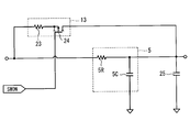
- FIG. 2 is a diagram showing a specific configuration of the burst current suppression circuit and the short circuit
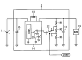
- FIG. 3 is a diagram showing the configuration of the power supply circuit.
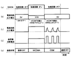
- 4 (a) to 4 (e) are diagrams showing a control sequence.
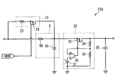
- FIG. 5 is a diagram illustrating a specific configuration of the burst current suppression circuit and the short circuit according to the second embodiment.
- FIG. 6 is a diagram illustrating a specific configuration of the burst current suppression circuit and the short circuit according to the third embodiment.
- FIG. 1 is a functional block diagram illustrating a configuration of a wireless communication apparatus according to the first embodiment.
- FIG. 2 is a diagram showing a specific configuration of the burst current suppression circuit and the short circuit
- FIG. 3 is a diagram showing the configuration of the power supply circuit.
- 4 (a) to 4 (e) are diagrams showing a control sequence.
- FIG. 5 is
- FIG. 7 is a functional block diagram showing the configuration of the wireless communication apparatus showing the fourth embodiment.
- FIG. 8 is a diagram showing a specific configuration of the burst current suppression circuit and the short circuit
- FIG. 9 is a functional block diagram showing a configuration of a wireless communication apparatus showing the prior art.
- the wireless communication device 11 which is a mobile phone is obtained by adding a control unit 12 and a short circuit 13 (bypass circuit) to the configuration shown in FIG.
- the short circuit 13 is connected in parallel to the burst current suppression circuit 5 (current fluctuation suppression circuit, integration circuit), and the control unit 12 outputs a control signal VCONT to switch the output voltage of the power supply circuit 2.
- the control unit 12 outputs a control signal SWON for short-circuiting the input and output of the burst current suppression circuit 5 by the short circuit 13.
- the control unit 12 and the communication device 3 transmit and receive commands and data by performing serial communication, for example.
- the communication device 3 transmits a command indicating whether the communication method being executed is, for example, WCDMA or GSM in response to a request from the control unit 12 or periodically.
- the power supply circuit 2 includes a DC / DC converter 14, and an input terminal of the DC / DC converter 14 is connected to a positive terminal of a power supply 1 (for example, a battery or a vehicle battery).
- the input capacitor 15 is connected to the power supply 1 in parallel.
- the DC / DC converter 14 steps down or boosts the power supply voltage from the power supply 1 and supplies it to the load 16 including the communication device 3 and the other circuit 4 shown in FIG.
- a series circuit of the output capacitor 17 and the resistor elements R1 to R3 (feedback resistors) is connected to the load 16 in parallel.
- the DC / DC converter 14 includes an inductor 18, a converter control unit (Cont.) 19 that controls switching of energization of the inductor 18, and an error amplifier 20.
- the reference voltage 21 is applied to the non-inverting input terminal of the error amplifier 20, and the output terminal c of the changeover switch 22 is connected to the inverting input terminal.
- Input terminals a and b of the changeover switch 22 are connected to a common connection point of the resistance elements R1 and R2 and a common connection point of the resistance elements R2 and R3, respectively.
- the changeover switch 22 switches the output terminal c to be connected to either the input terminal a or b in accordance with the control signal VCONT output from the control unit 12.
- the converter control unit 19 includes a switching element such as an FET and a circuit that controls switching by the element.
- the short circuit 13 is composed of a series circuit of a current limiting resistance element 23 and a P-channel MOSFET 24.
- One end of the resistance element 23 is connected to the input side of the burst current suppression circuit 5, and the drain of the P-channel MOSFET 24 is connected to the output side of the burst current suppression circuit 5.
- a control signal SWON output from the control unit 12 is applied to the gate of the P-channel MOSFET 24.
- the capacitor 25 connected to the output side of the burst current suppression circuit 5 stabilizes the power supply input to the communication device 5.
- the control unit 12 sets the control signal SWON to high level to turn off the short circuit 13 (FIG. 4A), and the burst current suppression circuit 5 Block the path that bypasses. Further, the output terminal c of the changeover switch 22 is connected to the input terminal b (FIG. 4B). At this time, the resistance values of the resistance elements R1 to R3 and the reference voltage 21 are set so that the output voltage of the power supply circuit 2 becomes 5V.
- the control unit 12 sets the control signal SWON to low level to turn on the short circuit 13 and connect the bypass path of the burst current suppression circuit 5. Moreover, it switches so that the output terminal c of the changeover switch 22 may be connected to the input terminal a.
- the output voltage of the power supply circuit 2 is set to 3.5V. For example, if the reference voltage 21 is 0.8V, the output voltage is 0.8V ⁇ ⁇ 1 + R1 / (R2 + R3) ⁇ .
- the current consumption of the communication device 3 is substantially constant (FIG. 4D), and therefore the output current of the power supply circuit 2 is also substantially constant (FIG. 4C). In this case, since the power output from the power supply circuit 2 bypasses the burst current suppression circuit 5 and is supplied to the communication device 3, it is avoided that power is unnecessarily consumed by the resistance element 5R.
- the control unit 12 turns off the short circuit 13 and switches the output terminal c of the changeover switch 22 to the input terminal b side.
- the output voltage of the power supply circuit 2 at this time is set to 5V because the voltage drop due to the resistance element R5 of the burst current suppression circuit 5 based on the consumption current is expected to be 1.5V and the power supplied to the communication device 3 is supplied. This is to maintain the voltage at 3.5V.
- the burst current suppression circuit 5 that suppresses the current fluctuation on the output side of the power supply circuit 2 is arranged, and the burst current A short circuit 13 is provided that intermittently connects a path that bypasses the suppression circuit 5.
- the control part 12 controls the short circuit 13 so that a bypass path may be formed, when the communication apparatus 3 performs the WCDMA system which does not employ
- the burst current suppression circuit 5 is an integration circuit including the resistance element 5R and the capacitor 5C, current fluctuation on the output side of the power supply circuit 2 can be suppressed with a simple configuration.
- the wireless communication device 31 shown in FIG. 5 is configured such that a series power supply circuit 32 (step-down power supply circuit) is disposed between the burst current suppression circuit 5 and the communication device 3.
- a P-channel MOSFET 33 is inserted in the power supply line.
- a series circuit of resistance elements 34 and 35 is connected between the drain of the P-channel MOSFET 33 and the ground.
- a common connection point of the resistance elements 34 and 35 is connected to a non-inverting input terminal of the operational amplifier 36, and a reference voltage 37 is applied to the inverting input terminal of the operational amplifier 36.
- the output terminal of the operational amplifier 36 is connected to the gate of the P-channel MOSFET 33.
- the series power supply circuit 32 By arranging the series power supply circuit 32, the power supply voltage supplied to the communication device 3 is smoothed when the voltage drop in the burst current suppression circuit 5 is large. Alternatively, when the operation voltage of the communication device 3 is set lower than the operation voltages of the other circuits 4, the power supply voltage by the series power supply circuit 32 is lowered and adjusted.
- the series power supply circuit 32 is arranged between the burst current suppression circuit 5 and the communication device 3, the power supply voltage supplied to the communication device 3 can be smoothed, The operating voltage of the other circuit 4 and the operating voltage of the communication device 3 can be adjusted to be appropriate voltages. Further, since the short circuit 13 is connected so as to be bypassed including the series power supply circuit 32, the power supply circuit 2 can be operated when it is not necessary to operate the series power supply circuit 32 if there is no voltage drop in the burst current suppression circuit 5. The power to be output can be directly supplied to the communication device 3.
- the short circuit 13 is connected in parallel only to the burst current suppression circuit 5. Therefore, unlike the second embodiment, even when there is no voltage drop in the burst current suppression circuit 5, it is possible to cope with the case where the series power supply circuit 32 needs to be operated.
- the resistance element Ri is inserted in the power supply line, and a series circuit of the resistance elements 44 and 45 is provided between the input side (series power circuit 32 side) terminal of the resistance element Ri and the ground. It is connected.
- the output side terminal of the resistance element Ri is connected to the inverting input terminal of the comparator 46, and the non-inverting input terminal of the comparator 46 is connected to the common connection point of the resistance elements 44 and 45.
- the output terminal of the comparator 46 is connected to the input terminal of the control unit 42. The above constitutes the current measurement circuit 43.
- the operation of the fourth embodiment will be described. If the communication device 3 is performing WCDMA communication and the current consumption by the communication device 3 is small, the potential of the inverting input terminal of the comparator 46 becomes larger than the threshold voltage applied to the non-inverting input terminal. Therefore, the current measurement circuit 43 outputs a low level signal to the control unit 42. On the other hand, when the communication device 3 performs GSM communication and the current consumption by the communication device 3 increases, the potential of the inverting input terminal of the comparator 46 becomes smaller than the threshold voltage. Then, the current measurement circuit 43 outputs a high level signal to the control unit 42 (only transmission timing in burst communication).
- 1 frame of communication in the GSM system is 4.6 ms. Therefore, the control unit 42 determines that the output signal level of the current measurement circuit 43 alternately repeats high and low within a period of one frame, so that the communication device 3 executes GSM communication. The output voltage of the power supply circuit 2 and the on / off of the short circuit 13 are switched.
- the current measurement circuit 43 that detects the current flowing through the power supply line is provided between the burst current suppression circuit 5 and the communication device 3, and the control unit 42 includes the current measurement circuit.
- the communication method being executed by the communication device 3 is determined according to the energization state of the current detected by 43, and the short circuit 13 is controlled. Therefore, for example, as in the first embodiment, the control unit 42 detects the change in the communication method more quickly than the configuration in which the communication device 3 transmits the communication method being executed to the control unit 12. it can.
- the communication device 3 and the control unit 12 do not necessarily perform communication.
- the communication device 3 outputs a binary signal to the control unit 12, and the communication method is switched by the change (high, low) of the signal. May be shown.
- the communication between the communication device 3 and the control unit 42 is performed in the same manner as in the first embodiment, indicating that the GSM communication indicated by the communication device 3 is being executed, and the current measurement circuit 43 Switching may be performed when the output signal level changes as described above.
- the series power supply circuit 32 may be deleted.
- the output voltage of the power supply circuit 2 may be set appropriately according to them.
- the current fluctuation suppression circuit may be any circuit that suppresses fluctuations in the output voltage of the power supply circuit 2, and is not limited to an integration circuit.
- the communication device may support three or more communication methods.
- a bipolar transistor may be used instead of the MOSFET.
- the specific configuration of the current detection circuit is not limited to the current measurement circuit 43.
- the communication method is not limited to WCDMA and GSM, and any communication method may be used as long as at least one communication method performs burst communication.
- the wireless communication device is not limited to a mobile phone.
Landscapes
- Engineering & Computer Science (AREA)
- Computer Networks & Wireless Communication (AREA)
- Signal Processing (AREA)
- Transceivers (AREA)
- Telephone Function (AREA)
- Transmitters (AREA)
Abstract
Description
以下、図9と同一部分には同一符号を付して説明を省略し、異なる部分について説明する。例えば携帯電話機である無線通信装置11は、図9に示す構成に、制御部12及び短絡回路13(バイパス回路)を加えたものである。短絡回路13は、バースト電流抑制回路5(電流変動抑制回路,積分回路)に並列に接続されており、制御部12は、電源回路2の出力電圧を切り替えるために制御信号VCONTを出力する。また、制御部12は、短絡回路13によりバースト電流抑制回路5の入出力間を短絡するための制御信号SWONを出力する。
以下、第1実施形態と同一部分には同一符号を付して説明を省略し、異なる部分についてのみ説明する。図5に示す無線通信装置31は、バースト電流抑制回路5と通信機3との間にシリーズ電源回路32(降圧型電源回路)を配置したものである。電源供給ラインには、PチャネルMOSFET33が挿入されている。PチャネルMOSFET33のドレインとグランドとの間には、抵抗素子34及び35の直列回路が接続されている。抵抗素子34及び35の共通接続点はオペアンプ36の非反転入力端子に接続され、オペアンプ36の反転入力端子には基準電圧37が与えられている。そして、オペアンプ36の出力端子は、PチャネルMOSFET33のゲートに接続されている。
図6に示す第3実施形態では、短絡回路13は、バースト電流抑制回路5に対してのみ並列に接続されている。したがって、第2実施形態とは異なり、バースト電流抑制回路5における電圧降下がなくても、シリーズ電源回路32を動作させる必要がある場合に対応することができる。
図7に示す無線通信装置41は、通信機3と制御部12に替わる制御部42とは、第1実施形態のように実行中である通信方式を伝達するための通信を行わない(但し、制御部42が通信機3を制御するための通信は行う)。そして、バースト電流抑制回路5と通信機3との間には、電流計測回路43(電流検出回路)が配置されている。そして、制御部42は、電流計測回路43により計測される通信機3への通電状態に応じて、通信機3が実行している通信方式を判定する。
Claims (5)
- 複数の通信方式に対応可能な無線通信部(3)と、
電源電圧を変圧して前記無線通信部に供給する電源回路(2)と、
前記無線通信部が実行する通信方式に応じて、前記電源回路の出力電圧を制御する制御部(12)と、
前記無線通信部が、前記通信方式の1つ以上で採用されている、信号の送信を間欠的に繰り返し実行するバースト通信を実行する際に、前記電源回路の出力側における電流変動を抑制するために配置される電流変動抑制回路(5)と、
この電流変動抑制回路をバイパスするバイパス経路を断続するためのバイパス回路(13)とを備え、
前記制御部は、前記無線通信部が実行する通信方式に応じて前記バイパス回路を制御し、前記無線通信部が前記バースト通信を採用しない通信方式を実行する際に前記バイパス経路を形成する無線通信装置。 - 前記電流変動抑制回路(5)は、積分回路で構成される請求項1記載の無線通信装置。
- 前記電流変動抑制回路と前記無線通信部との間に配置された、降圧型電源回路(32)をさらに有する請求項1又は2記載の無線通信装置。
- 前記バイパス回路は、前記降圧型電源回路も含んでバイパスするように、前記バイパス経路を形成する請求項3記載の無線通信装置。
- 前記電流変動抑制回路と前記無線通信部との間に、電源供給ラインに流れる電流を検出する電流検出回路(43)をさらに備え、
前記制御部(42)は、前記電流検出回路によって検出される電流の通電状態に応じて、前記バイパス回路を制御する請求項1から4の何れか一項に記載の無線通信装置。
Priority Applications (2)
| Application Number | Priority Date | Filing Date | Title |
|---|---|---|---|
| DE112013006052.3T DE112013006052B4 (de) | 2012-12-18 | 2013-11-26 | Drahtloskommunikationsvorrichtung |
| US14/653,188 US9473255B2 (en) | 2012-12-18 | 2013-11-26 | Wireless communication device |
Applications Claiming Priority (2)
| Application Number | Priority Date | Filing Date | Title |
|---|---|---|---|
| JP2012275690A JP6020127B2 (ja) | 2012-12-18 | 2012-12-18 | 無線通信装置 |
| JP2012-275690 | 2012-12-18 |
Publications (1)
| Publication Number | Publication Date |
|---|---|
| WO2014097547A1 true WO2014097547A1 (ja) | 2014-06-26 |
Family
ID=50977912
Family Applications (1)
| Application Number | Title | Priority Date | Filing Date |
|---|---|---|---|
| PCT/JP2013/006924 Ceased WO2014097547A1 (ja) | 2012-12-18 | 2013-11-26 | 無線通信装置 |
Country Status (4)
| Country | Link |
|---|---|
| US (1) | US9473255B2 (ja) |
| JP (1) | JP6020127B2 (ja) |
| DE (1) | DE112013006052B4 (ja) |
| WO (1) | WO2014097547A1 (ja) |
Citations (2)
| Publication number | Priority date | Publication date | Assignee | Title |
|---|---|---|---|---|
| JPH07307696A (ja) * | 1994-05-12 | 1995-11-21 | Oki Electric Ind Co Ltd | 携帯電子装置 |
| JP2006279577A (ja) * | 2005-03-29 | 2006-10-12 | Fujitsu Ltd | デュアルモード通信方法およびデュアルモード通信端末 |
Family Cites Families (5)
| Publication number | Priority date | Publication date | Assignee | Title |
|---|---|---|---|---|
| EP0954082A3 (en) * | 1998-04-10 | 1999-11-24 | Kabushiki Kaisha Toshiba | AC transmission system |
| JP2004297753A (ja) * | 2003-02-07 | 2004-10-21 | Nec Tokin Corp | 電源回路、及び該電源回路を備えた通信機器 |
| JP2005175561A (ja) | 2003-12-08 | 2005-06-30 | Renesas Technology Corp | 高周波電力増幅回路用電源回路および電源用半導体集積回路並びに電源用電子部品 |
| JP4285550B2 (ja) | 2007-02-15 | 2009-06-24 | 株式会社デンソー | 車載用緊急通報装置 |
| JP2010118918A (ja) | 2008-11-13 | 2010-05-27 | Nec Corp | 無線通信装置、電力増幅器の電源電圧制御方法 |
-
2012
- 2012-12-18 JP JP2012275690A patent/JP6020127B2/ja not_active Expired - Fee Related
-
2013
- 2013-11-26 WO PCT/JP2013/006924 patent/WO2014097547A1/ja not_active Ceased
- 2013-11-26 DE DE112013006052.3T patent/DE112013006052B4/de not_active Expired - Fee Related
- 2013-11-26 US US14/653,188 patent/US9473255B2/en active Active
Patent Citations (2)
| Publication number | Priority date | Publication date | Assignee | Title |
|---|---|---|---|---|
| JPH07307696A (ja) * | 1994-05-12 | 1995-11-21 | Oki Electric Ind Co Ltd | 携帯電子装置 |
| JP2006279577A (ja) * | 2005-03-29 | 2006-10-12 | Fujitsu Ltd | デュアルモード通信方法およびデュアルモード通信端末 |
Also Published As
| Publication number | Publication date |
|---|---|
| JP6020127B2 (ja) | 2016-11-02 |
| US20150333848A1 (en) | 2015-11-19 |
| JP2014120985A (ja) | 2014-06-30 |
| DE112013006052B4 (de) | 2020-11-12 |
| US9473255B2 (en) | 2016-10-18 |
| DE112013006052T5 (de) | 2015-09-10 |
Similar Documents
| Publication | Publication Date | Title |
|---|---|---|
| US9058043B2 (en) | Voltage converter for generating output signal with steady ripple | |
| US8391805B2 (en) | Radio frequency switch | |
| TWI682625B (zh) | 用於功率放大器的供應調變器的裝置及方法 | |
| US8698473B2 (en) | Switching regulator | |
| CN107134923B (zh) | 开关调节器 | |
| KR20150075034A (ko) | 스위칭 레귤레이터 및 전자 기기 | |
| US8854025B2 (en) | Switching power supply | |
| US10218195B2 (en) | Switching-type charging circuit capable of quickly dropping the voltage at the input end to zero | |
| US10079538B2 (en) | Bootstrap circuit for DC/DC converter | |
| US9780653B2 (en) | DC-DC converter | |
| US20200092830A1 (en) | Quick-start high-voltage boost | |
| JP5842483B2 (ja) | 2次電池用電源装置及び車載器 | |
| US20150253743A1 (en) | Control circuit including load switch, electronic apparatus including the load switch, and control method thereof | |
| JP4704918B2 (ja) | スイッチングレギュレータ | |
| US8396443B2 (en) | Power supply circuit and receiving apparatus | |
| JP6020127B2 (ja) | 無線通信装置 | |
| US20170229958A1 (en) | Switching regulator | |
| JP6352733B2 (ja) | 電源回路及びその制御方法 | |
| US8198879B2 (en) | Booster circuit and PWM signal generator | |
| JP5641555B2 (ja) | Dcdcコンバータおよびその起動制御方法 | |
| KR101335654B1 (ko) | 전력스위치 채널 폭 제어 장치 | |
| CN110739916A (zh) | 供电电路和终端设备 | |
| TW200536227A (en) | Switchable power supply system and method thereof | |
| JP2018093292A (ja) | スイッチング回路 |
Legal Events
| Date | Code | Title | Description |
|---|---|---|---|
| 121 | Ep: the epo has been informed by wipo that ep was designated in this application |
Ref document number: 13863981 Country of ref document: EP Kind code of ref document: A1 |
|
| WWE | Wipo information: entry into national phase |
Ref document number: 14653188 Country of ref document: US |
|
| WWE | Wipo information: entry into national phase |
Ref document number: 112013006052 Country of ref document: DE Ref document number: 1120130060523 Country of ref document: DE |
|
| 122 | Ep: pct application non-entry in european phase |
Ref document number: 13863981 Country of ref document: EP Kind code of ref document: A1 |