WO2014080674A1 - 撮像装置、デフォーカス量演算方法、及び撮像光学系 - Google Patents
撮像装置、デフォーカス量演算方法、及び撮像光学系 Download PDFInfo
- Publication number
- WO2014080674A1 WO2014080674A1 PCT/JP2013/073391 JP2013073391W WO2014080674A1 WO 2014080674 A1 WO2014080674 A1 WO 2014080674A1 JP 2013073391 W JP2013073391 W JP 2013073391W WO 2014080674 A1 WO2014080674 A1 WO 2014080674A1
- Authority
- WO
- WIPO (PCT)
- Prior art keywords
- phase difference
- difference detection
- imaging
- pair
- pixel
- Prior art date
- Legal status (The legal status is an assumption and is not a legal conclusion. Google has not performed a legal analysis and makes no representation as to the accuracy of the status listed.)
- Ceased
Links
Images







Classifications
-
- G—PHYSICS
- G02—OPTICS
- G02B—OPTICAL ELEMENTS, SYSTEMS OR APPARATUS
- G02B7/00—Mountings, adjusting means, or light-tight connections, for optical elements
- G02B7/28—Systems for automatic generation of focusing signals
- G02B7/34—Systems for automatic generation of focusing signals using different areas in a pupil plane
-
- H—ELECTRICITY
- H04—ELECTRIC COMMUNICATION TECHNIQUE
- H04N—PICTORIAL COMMUNICATION, e.g. TELEVISION
- H04N23/00—Cameras or camera modules comprising electronic image sensors; Control thereof
- H04N23/60—Control of cameras or camera modules
- H04N23/67—Focus control based on electronic image sensor signals
- H04N23/672—Focus control based on electronic image sensor signals based on the phase difference signals
-
- G—PHYSICS
- G02—OPTICS
- G02B—OPTICAL ELEMENTS, SYSTEMS OR APPARATUS
- G02B13/00—Optical objectives specially designed for the purposes specified below
- G02B13/001—Miniaturised objectives for electronic devices, e.g. portable telephones, webcams, PDAs, small digital cameras
-
- G—PHYSICS
- G03—PHOTOGRAPHY; CINEMATOGRAPHY; ANALOGOUS TECHNIQUES USING WAVES OTHER THAN OPTICAL WAVES; ELECTROGRAPHY; HOLOGRAPHY
- G03B—APPARATUS OR ARRANGEMENTS FOR TAKING PHOTOGRAPHS OR FOR PROJECTING OR VIEWING THEM; APPARATUS OR ARRANGEMENTS EMPLOYING ANALOGOUS TECHNIQUES USING WAVES OTHER THAN OPTICAL WAVES; ACCESSORIES THEREFOR
- G03B13/00—Viewfinders; Focusing aids for cameras; Means for focusing for cameras; Autofocus systems for cameras
- G03B13/32—Means for focusing
- G03B13/34—Power focusing
- G03B13/36—Autofocus systems
-
- H—ELECTRICITY
- H04—ELECTRIC COMMUNICATION TECHNIQUE
- H04N—PICTORIAL COMMUNICATION, e.g. TELEVISION
- H04N23/00—Cameras or camera modules comprising electronic image sensors; Control thereof
- H04N23/50—Constructional details
- H04N23/55—Optical parts specially adapted for electronic image sensors; Mounting thereof
-
- H—ELECTRICITY
- H04—ELECTRIC COMMUNICATION TECHNIQUE
- H04N—PICTORIAL COMMUNICATION, e.g. TELEVISION
- H04N25/00—Circuitry of solid-state image sensors [SSIS]; Control thereof
- H04N25/10—Circuitry of solid-state image sensors [SSIS]; Control thereof for transforming different wavelengths into image signals
- H04N25/11—Arrangement of colour filter arrays [CFA]; Filter mosaics
- H04N25/13—Arrangement of colour filter arrays [CFA]; Filter mosaics characterised by the spectral characteristics of the filter elements
- H04N25/134—Arrangement of colour filter arrays [CFA]; Filter mosaics characterised by the spectral characteristics of the filter elements based on three different wavelength filter elements
-
- H—ELECTRICITY
- H04—ELECTRIC COMMUNICATION TECHNIQUE
- H04N—PICTORIAL COMMUNICATION, e.g. TELEVISION
- H04N25/00—Circuitry of solid-state image sensors [SSIS]; Control thereof
- H04N25/70—SSIS architectures; Circuits associated therewith
- H04N25/703—SSIS architectures incorporating pixels for producing signals other than image signals
- H04N25/704—Pixels specially adapted for focusing, e.g. phase difference pixel sets
Definitions
- the present invention relates to an imaging apparatus, a defocus amount calculation method, and an imaging optical system.
- an imaging device In recent years, with the increase in the resolution of solid-state imaging devices such as CCD (Charge Coupled Device) image sensors and CMOS (Complementary Metal Oxide Semiconductor) image sensors, mobile phones such as digital still cameras, digital video cameras, and smartphones, PDA (Personal Digital). Demand for information equipment having a photographing function such as an assistant (mobile information terminal) is rapidly increasing. Note that an information device having the above imaging function is referred to as an imaging device.
- CCD Charge Coupled Device
- CMOS Complementary Metal Oxide Semiconductor
- These imaging apparatuses employ a contrast AF (Auto Focus) method or a phase difference AF method as a focus control method for detecting a distance to a main subject and focusing on the subject. Since the phase difference AF method can detect the in-focus position at a higher speed than the contrast AF method, it is widely used in various imaging devices (see Patent Documents 1 to 3).
- a contrast AF Auto Focus
- a phase difference AF method can detect the in-focus position at a higher speed than the contrast AF method, it is widely used in various imaging devices (see Patent Documents 1 to 3).
- Patent Document 1 discloses an imaging apparatus that performs phase difference AF using a signal read from a pixel for phase difference detection, with some of the pixels of the image sensor as pixels for phase difference detection. Patent Document 1 describes that a gain difference due to lens vignetting occurs between a pair of image signals for which a phase difference is to be calculated, and in each pixel of a pair of image signals whose phases are matched. A method for correcting this gain difference based on the pixel output ratio distribution is described.
- Patent Documents 2 and 3 disclose an imaging apparatus that improves AF accuracy by performing phase difference AF after correcting data that causes a decrease in phase difference AF accuracy using a correction value generated for each lens. Is described.
- the phase difference detection pixel includes a right pixel that detects light that has passed through, for example, the right half of the pupil region of the photographing optical system, and a left pixel that detects light that has passed through, for example, the left half of the pupil region of the photographing optical system. At least two types are used.
- the right and left pixels differ in sensitivity even if the image height of the image sensor (distance from the point where it intersects the optical axis of the imaging optical system in the area where the pixels are located) is the same due to the difference in incident angle sensitivity characteristics. Will occur. That is, there is a level difference between the output signals of the pair of phase difference detection pixels arranged in close proximity.
- Patent Document 1 discloses a method of obtaining a gain difference between a pair of image signals from a pair of image signals obtained by imaging and correcting the gain difference. However, since this method obtains the gain difference from the signal obtained by imaging, the amount of calculation until the gain difference is corrected increases, and the AF speed decreases.
- Patent Documents 2 and 3 do not consider the correction of the level difference of the output signal of the phase difference detection pixel pair.
- the present invention has been made in view of the above circumstances, and improves the phase difference AF speed and the phase difference AF accuracy by accurately correcting the level difference of the output signals of the pair of phase difference detection pixels with a simple configuration. It is an object of the present invention to provide an imaging device and a defocus amount calculation method that can perform this.
- An imaging apparatus is an imaging apparatus in which an imaging optical system is detachable, and includes a plurality of imaging pixels that capture an image formed by a light beam that has passed through a pupil region of the imaging optical system, and the imaging optical system.
- a plurality of first phase difference detection pixels that capture one of a pair of images formed by a pair of light beams that have passed through different parts of the pupil region, and a plurality of second positions that capture the other of the pair of images
- the imaging element including the light receiving surface on which the phase difference detection pixels are arranged, and the information on the different incident light beam angles at arbitrary positions in the shift direction of the pair of images on the light receiving surface, the first position at the arbitrary position.
- the sensitivity ratio between one phase difference detection pixel and the imaging pixel adjacent thereto, and the sensitivity between the second phase difference detection pixel located at the arbitrary position and the imaging pixel adjacent thereto The first note that stores sensitivity ratio data indicating the ratio
- the imaging optical system includes information on incident light angle of a light beam incident through the imaging optical system at each of at least two positions in the displacement direction of the light receiving surface.
- a second storage unit for storing each optical condition of the system is provided, and the information on the incident ray angle at the at least two positions corresponding to the set optical condition is acquired from the second storage unit and acquired.
- the first phase difference detection pixel and the first phase difference detection pixel are disposed in proximity to the first phase difference detection pixel.
- the defocus amount calculation method of the present invention is a defocus amount calculation method by an imaging device to which an imaging optical system can be attached and detached, wherein the imaging device is an image formed by a light beam that has passed through the pupil region of the imaging optical system.
- An image pickup device including a light receiving surface on which a plurality of second phase difference detection pixels for picking up the other of the pair of images is disposed, and different incident light rays at arbitrary positions in the shift direction of the pair of images on the light receiving surface.
- a first storage unit that stores sensitivity ratio data indicating a sensitivity ratio with the imaging pixel, and the imaging optical system includes the imaging at each of at least two positions in the shift direction of the light receiving surface.
- a second storage unit that stores information on an incident light angle of a light beam incident through the optical system for each optical condition of the imaging optical system is provided, and the at least two positions corresponding to the set optical condition Using the sensitivity ratio data stored in the first storage unit corresponding to each of the plurality of information on the incident light beam angles obtained from the second storage unit.
- Use the output signal of In which and a defocus amount calculation step of calculating a defocus amount Te.
- the imaging optical system of the present invention is an imaging optical system that is mounted on an imaging apparatus having a mount mechanism, and includes the second storage unit.
- an imaging apparatus and a defocus amount capable of accurately correcting a level difference of output signals of a pair of phase difference detection pixels with a simple configuration to improve phase difference AF speed and phase difference AF accuracy.
- An arithmetic method can be provided.
- FIG. 1 The figure which shows schematic structure of the digital camera as an example of the imaging device for describing one Embodiment of this invention
- the elements on larger scale which show the plane structure of the solid-state image sensor 5 mounted in the digital camera shown in FIG. 1 is a schematic plan view showing the overall configuration of a solid-state imaging device 5 mounted on the digital camera shown in FIG.
- the figure for demonstrating the incident ray angle in the arbitrary positions in the row direction X of the solid-state image sensor 5 The figure which shows an example of the table memorize
- movement of the digital camera shown in FIG. The figure for demonstrating the linear interpolation process of the sensitivity ratio of the digital camera shown in FIG.
- FIG. 1 is a diagram showing a schematic configuration of a digital camera as an example of an imaging apparatus for explaining an embodiment of the present invention.
- the digital camera shown in FIG. 1 includes a lens device 100 as an imaging optical system and a camera body 200 including a mount mechanism (not shown) on which the lens device 100 is mounted.
- the lens apparatus 100 includes a photographing lens 1 including a focus lens, a zoom lens, and the like, an aperture 2, a memory 3, a lens driving unit 8, and a lens driving unit 9.
- the lens device 100 can be attached to and detached from the camera body, and can be replaced with another one.
- the memory 3 can be accessed by a system control unit 11 described later of the camera body 200.
- the camera body 200 includes a CCD type or CMOS type solid-state imaging device 5 provided behind the lens device 100, and an analog signal that performs analog signal processing such as correlated double sampling processing connected to the output of the solid-state imaging device 5.
- a processing unit 6 and an A / D conversion circuit 7 that converts an analog signal output from the analog signal processing unit 6 into a digital signal are provided.
- the analog signal processing unit 6 and the A / D conversion circuit 7 are controlled by the system control unit 11.
- the analog signal processing unit 6 and the A / D conversion circuit 7 may be built in the solid-state imaging device 5.
- a system control unit 11 that performs overall control of the entire electric control system of the digital camera controls the lens driving unit 8 to adjust the position of the focus lens included in the photographing lens 1 or the position of the zoom lens included in the photographing lens 1. Make adjustments. Further, the system control unit 11 adjusts the exposure amount by controlling the aperture amount of the aperture 2 via the aperture drive unit 9.
- system control unit 11 drives the solid-state imaging device 5 via the imaging device driving unit 10 and outputs a subject image captured through the photographing lens 1 as a captured image signal.
- An instruction signal from the user is input to the system control unit 11 through the operation unit 14.
- the electric control system of the digital camera further performs interpolation calculation and gamma correction calculation on the main memory 16, the memory control unit 15 connected to the main memory 16, and the captured image signal output from the A / D conversion circuit 7. And a digital signal processing unit 17 that generates captured image data by performing RGB / YC conversion processing and the like, and the captured image data generated by the digital signal processing unit 17 is compressed into a JPEG format or the compressed image data is expanded.
- a display control unit 22 to be connected.
- the memory control unit 15, digital signal processing unit 17, compression / decompression processing unit 18, defocus amount calculation unit 19, external memory control unit 20, and display control unit 22 are mutually connected by a control bus 24 and a data bus 25. It is controlled by a command from the system control unit 11.
- FIG. 2 is a partially enlarged view showing a planar configuration of the solid-state imaging device 5 mounted on the digital camera shown in FIG.
- the solid-state imaging device 5 includes a large number of pixels 51 (each square block in the figure) arranged two-dimensionally in a row direction X and a column direction Y orthogonal thereto. Although all the pixels 51 are not shown in FIG. 2, in reality, about several million to several tens of thousands of pixels 51 are two-dimensionally arranged.
- an output signal is obtained from each of the large number of pixels 51. This set of output signals is referred to as a captured image signal in this specification.
- Each pixel 51 includes a photoelectric conversion unit such as a photodiode and a color filter formed above the photoelectric conversion unit.
- a pixel “R” is attached to the pixel 51 including a color filter that transmits red light
- a letter “G” is attached to the pixel 51 that includes a color filter that transmits green light.
- the pixel 51 including the color filter that passes through is marked with the letter “B”.
- the large number of pixels 51 is an array in which a plurality of pixel rows including a plurality of pixels 51 arranged in the row direction X are arranged in the column direction Y. Then, the odd-numbered pixel rows and the even-numbered pixel rows are shifted in the row direction X by about 1 ⁇ 2 of the arrangement pitch of the pixels 51 of each pixel row.
- the array of color filters included in each pixel 51 of the odd-numbered pixel row is a Bayer array as a whole. Further, the color filter array included in each pixel 51 of the even-numbered pixel row is also a Bayer array as a whole.
- the pixels 51 in the odd-numbered rows and the pixels 51 adjacent to the lower right of the pixels 51 and detecting the same color light as the pixels 51 form a pair pixel.
- the solid-state imaging device 5 having such a pixel arrangement, it is possible to increase the sensitivity of the camera by adding the output signals of the two pixels 51 that constitute the paired pixels, or the two pixels 51 that constitute the paired pixels. By changing the exposure time and adding the output signals of the two pixels 51, the camera can have a wide dynamic range.
- some of the large number of pixels 51 are phase difference detection pixels.
- the phase difference detection pixels include a plurality of phase difference detection pixels 51R and a plurality of phase difference detection pixels 51L.
- the plurality of phase difference detection pixels 51R receive one of a pair of light beams that have passed through different portions of the pupil region of the photographing lens 1 (for example, a light beam that has passed through the right half of the pupil region) and output a signal corresponding to the amount of light received. To do. That is, the plurality of phase difference detection pixels 51R provided in the solid-state imaging device 5 capture an image formed by one of the pair of light beams.
- the plurality of phase difference detection pixels 51L receive the other of the pair of light beams (for example, a light beam that has passed through the left half of the pupil region) and output a signal corresponding to the amount of light received. That is, the plurality of phase difference detection pixels 51L provided in the solid-state imaging device 5 capture an image formed by the other of the pair of light beams.
- a plurality of pixels 51 (hereinafter referred to as imaging pixels) other than the phase difference detection pixels 51R and 51L capture an image formed by a light beam that has passed through almost all of the pupil region of the photographing lens 1. It becomes.
- a light shielding film is provided above the photoelectric conversion unit of the pixel 51, and an opening that defines a light receiving area of the photoelectric conversion unit is formed in the light shielding film.
- the center of the aperture of the imaging pixel 51 coincides with the center of the photoelectric conversion unit of the imaging pixel 51 (the center of the square block).
- the center of the photoelectric conversion unit of the imaging pixel 51 the center of the square block.
- FIG. 2 in order to simplify the drawing, only a part of the imaging pixel 51 is illustrated with an opening a.
- the center of the opening (indicated by symbol c in FIG. 2) of the phase difference detection pixel 51R is eccentric to the right with respect to the center of the photoelectric conversion unit of the phase difference detection pixel 51R.
- the center of the opening (indicated by symbol b in FIG. 2) of the phase difference detection pixel 51L is eccentric to the left with respect to the center of the photoelectric conversion unit of the phase difference detection pixel 51L.
- a part of the pixel 51 on which the green color filter is mounted is the phase difference detection pixel 51R or the phase difference detection pixel 51L.
- a pixel on which a color filter of another color is mounted may be used as a phase difference detection pixel.
- phase difference pairs Pairs of the phase difference detection pixels 51R and the phase difference detection pixels 51L arranged in the vicinity thereof (hereinafter referred to as phase difference pairs) are discrete and periodic on the light receiving surface 50 on which the pixels 51 are arranged. Are arranged.
- the two adjacent pixels mean two pixels that are close enough to be regarded as receiving light from substantially the same subject portion. Since the phase difference detection pixel 51R and the phase difference detection pixel 51L constituting the phase difference pair are close to each other, they are treated as having the same position in the row direction X (hereinafter also referred to as a horizontal pixel position).
- the phase difference detection pixels 51 ⁇ / b> R are arranged at intervals of three pixels in the row direction X in a part of even-numbered pixel rows (four pixel rows arranged every three pixel rows in the example of FIG. 2). Is arranged.
- the phase difference detection pixel 51 ⁇ / b> L detects the phase difference in the row direction X in a part of the odd-numbered pixel rows (the pixel row adjacent to the pixel row including the phase difference detection pixels 51 ⁇ / b> R).
- the pixels 51R are arranged in the same cycle.
- the light received by the phase difference detection pixel 51L through the opening b of the light shielding film is light from the left side when viewed from the subject of the photographing lens 1 provided above the paper surface of FIG. Mainly comes from the direction of the right eye.
- the light received by the phase difference detection pixel 51R through the opening c of the light shielding film is light from the right side when viewed from the subject of the photographing lens 1, that is, light from the direction of viewing the subject with the left eye. Become the Lord.
- a captured image signal obtained by viewing the subject with the left eye can be obtained by all the phase difference detection pixels 51R, and a captured image signal obtained by viewing the subject by the right eye can be obtained by all the phase difference detection pixels 51L. be able to. For this reason, it is possible to generate stereoscopic image data of a subject by combining the both, or to generate phase difference information by performing a correlation calculation between the two.
- the phase difference detection pixel 51R and the phase difference detection pixel 51L can receive light beams that have passed through different parts of the pupil region of the photographing lens 1 by decentering the opening of the light shielding film in the opposite direction. Phase difference information can be obtained.
- the structure for obtaining the phase difference information is not limited to this, and a well-known structure can be adopted.
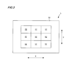
- FIG. 3 is a schematic plan view showing the overall configuration of the solid-state imaging device 5 mounted on the digital camera shown in FIG.
- the solid-state imaging device 5 has a light receiving surface 50 on which all the pixels 51 are arranged.
- AF areas phase difference detection areas
- the AF area 52 is an area including a plurality of phase difference pairs arranged in the row direction X. Only the imaging pixels 51 are arranged in a portion of the light receiving surface 50 excluding the AF area 52.
- the three AF areas 52 in the middle in the row direction X each pass through the intersection of the light receiving surface 50 with the optical axis of the imaging lens 1 in the plan view and in the column direction.
- This is an area having a width in the row direction X across the straight line extending in the Y direction.
- the position in the row direction X of the intersection of the light receiving surface 50 with the optical axis of the imaging lens 1 is referred to as the optical axis position.
- the defocus amount calculation unit 19 shown in FIG. 1 reads out from the phase difference detection pixel 51L and the phase difference detection pixel 51R in one AF area 52 selected from among the nine AF areas 52 by a user operation or the like. Using the output signal group, a phase difference amount that is a relative positional shift amount between the two images formed by the pair of light beams is calculated. Then, based on this phase difference amount, the focus adjustment state of the taking lens 1, here, the amount away from the in-focus state and its direction, that is, the defocus amount, are obtained.
- the system control unit 11 illustrated in FIG. 1 moves the focus lens included in the imaging lens 1 to the in-focus position based on the defocus amount calculated by the defocus amount calculation unit 19, and focuses the imaging lens 1. Control the state.
- the opening of the phase difference detection pixel 51R and the phase difference detection pixel 51L is eccentric in the opposite direction. For this reason, even if the positions of the openings in the eccentric direction (the displacement direction of the pair of images; the row direction X in FIG. 2) are substantially the same, there is a sensitivity difference between the phase difference detection pixel 51R and the phase difference detection pixel 51L. Will occur.
- FIG. 4 is a diagram showing the sensitivity ratio of the phase difference detection pixels 51R and 51L constituting the phase difference pair at an arbitrary position in the row direction X (hereinafter also referred to as a horizontal pixel position) in the solid-state imaging device 5.
- the straight line indicated by reference numeral 51R indicates the sensitivity ratio of the phase difference detection pixel 51R
- the straight line indicated by reference numeral 51L indicates the sensitivity ratio of the phase difference detection pixel 51L.
- the sensitivity ratio of an arbitrary phase difference detection pixel is the output signal of an arbitrary phase difference detection pixel and an imaging pixel adjacent thereto (however, that detects light of the same color as the arbitrary phase difference detection pixel).
- a and B respectively, it means a value represented by A / B or B / A.
- FIG. 4 shows the sensitivity when the sensitivity ratio is A / B.
- the range of the horizontal pixel positions of the three AF areas 52 at the left end in FIG. 3 is indicated by reference numeral 52L.
- the horizontal pixel position range of the three AF areas 52 at the center is indicated by reference numeral 52C.
- the range of the horizontal pixel position of the three AF areas 52 at the right end is indicated by reference numeral 52R.
- the horizontal pixel position at the left end of the range 52L is indicated by x1
- the horizontal pixel position at the right end of the range 52L is indicated by x2
- the horizontal pixel position at the right end of the range 52C is indicated by x3
- the right end of the range 52R is indicated by x4.
- phase difference detection pixels 51R and 51L are also periodically arranged in the column direction Y. However, since the openings of the phase difference detection pixel 51R and the phase difference detection pixel 51L are not decentered in the column direction Y, the sensitivity ratio is as shown in FIG.
- the sensitivity distribution of the phase difference detection pixels can be known by obtaining the sensitivity ratio, which is the ratio between the phase difference detection pixels and the output signals of the imaging pixels adjacent thereto.
- the opening c is eccentric to the right side in FIG.
- half of the light that has passed through the left side of the photographing lens 1 enters the opening c of the phase difference detection pixel 51 ⁇ / b> R at the left end of the light receiving surface 50, and the right side of the photographing lens 1.
- Light that has passed through will not enter.
- half of the light that has passed through the right side of the photographic lens 1 enters the opening c of the phase difference detection pixel 51R at the right end of the light receiving surface 50, and all the light that has passed through the left side of the photographic lens 1 enters. .
- only the light passing through the left side of the photographing lens 1 enters the opening c of the phase difference detection pixel 51R at the center of the light receiving surface 50, and the light passing through the right side of the photographing lens 1 cannot enter.
- the sensitivity ratio characteristic of the phase difference detection pixel 51L is opposite to that of the phase difference detection pixel 51R.
- the sensitivity ratio of the phase difference detection pixel 51L decreases from the left end portion of the light receiving surface 50 toward the right end portion.
- the sensitivity ratio of the phase difference detection pixel 51 ⁇ / b> R increases as it goes from the left end portion to the right end portion of the light receiving surface 50.
- the sensitivity ratio of the phase difference detection pixel 51L and the sensitivity ratio of the phase difference detection pixel 51R are substantially the same.
- the solid-state imaging device 5 on which the phase difference detection pixel 51R and the phase difference detection pixel 51L are mounted has a sensitivity ratio characteristic as shown in FIG. For this reason, a level difference occurs in the output signal between the phase difference detection pixel 51R and the phase difference detection pixel 51L constituting the phase difference pair, except for the vicinity of the optical axis position in the horizontal pixel position. Therefore, it is necessary to calculate the phase difference amount after correcting the level difference.
- the sensitivity ratio of each phase difference pair at an arbitrary horizontal pixel position shown in FIG. 4 is uniquely determined by the angle of light rays incident on the horizontal pixel position (hereinafter referred to as incident light beam angle).
- incident light beam angle the angle of light rays incident on the horizontal pixel position
- FIG. 6 is a view of the photographing lens 1 and the solid-state imaging device 5 when viewed in the column direction Y, which is a direction perpendicular to the optical axis of the photographing lens 1 and perpendicular to the row direction X.
- Light incident on an arbitrary horizontal pixel position of the solid-state imaging device 5 includes a principal ray passing through the center of the photographing lens 1, an upper ray passing through the upper end portion in FIG. 6 of the photographing lens 1, and a lower end in FIG. And a lower ray passing through the section.
- the upper light beam means a light beam that passes through one end portion (upper end portion) in the column direction Y of the photographing lens 1 and reaches the arbitrary horizontal pixel position.
- the lower light beam means a light beam that passes through the other end (lower end) in the column direction Y of the photographing lens 1 and reaches the arbitrary horizontal pixel position.
- the angle formed by the optical axis K of the photographic lens 1 and the upper light beam is ⁇ up, and the angle formed by the optical axis K of the photographic lens 1 and the lower light beam (lower light beam angle).
- the lower theta, incident light angle at an arbitrary horizontal pixel position of the solid-state imaging device 5 is defined above ray angle theta upper and lower ray angle theta combinations below.
- the incident light angle at the horizontal pixel position changes when the optical conditions of the imaging optical system (combination of F value, focal length, and focus lens position) change.
- the sensitivity ratio between the phase difference detection pixel 51R and the phase difference detection pixel 51L has a linear characteristic as shown in FIG. For this reason, if the sensitivity ratio between the phase difference detection pixel 51R and the phase difference detection pixel 51L at at least two positions in the row direction X of the solid-state imaging device 5 is known, the phase difference detection at all positions in the row direction X is known.
- the sensitivity ratio between the pixel for use 51R and the pixel for detection of phase difference 51L can be obtained by linear interpolation.
- the sensitivity ratio of each phase difference pair at an arbitrary horizontal pixel position is determined by the incident ray angle at that horizontal pixel position. Further, the incident ray angle at an arbitrary horizontal pixel position varies depending on the type of the lens device 100 and the optical conditions set in the lens device 100.
- the lens apparatus 100 when the lens apparatus 100 is attached to the camera body 200, information on incident light angle at at least two arbitrary positions in the row direction X of the solid-state imaging device 5 is obtained for each optical condition of the lens apparatus 100. And stored in the memory 3 of the lens apparatus 100 in advance.
- the main memory 16 of the camera body 200 stores a table in which the sensitivity ratios of the phase difference pairs at the arbitrary horizontal pixel positions are associated with the different incident light ray angles at the arbitrary horizontal pixel positions. Yes. Note that if the combination of the lens device and the image sensor is different, the sensitivity ratio of the phase difference pair will also be different. Therefore, it is desirable to store the data of the sensitivity ratio with respect to the incident light angle in the device equipped with the image sensor. Since the light angle information is determined by the lens, it is desirable to store it in the lens device.
- the information on the incident light angle stored in the memory 3 and the table data stored in the main memory 16 can be obtained by actual measurement in the adjustment process before shipment of the lens device 100 and the camera body 200.
- the incident light angle at each of the horizontal pixel positions x1, x2, x3, and x4 shown in FIG. 4 is measured for every optical condition (1, 2, 3,...) That can be set in the lens device 100.
- a table as shown in FIG. 7 is created from the measurement result and stored in the memory 3 of the lens apparatus 100.
- the sensitivity ratio of each of the phase difference detection pixel 51R and the phase difference detection pixel 51L having the same horizontal pixel position is measured.
- a table as shown in FIG. 7 is created from the measurement results and stored in the main memory 16 of the camera body 200.
- the sensitivity ratio of the phase difference detection pixel 51R is indicated by R1, R2, and R3
- the sensitivity ratio of the phase difference detection pixel 51L is indicated by L1, L2, and L3.
- the system control unit 11 corrects the level difference of the output signal of the phase difference pair using the information stored in the memory 3 of the lens device 100 and the table stored in the main memory 16. For example, a correction coefficient for correcting the level difference of the output signal of the phase difference pair is generated, and the level difference of the output signal of the phase difference pair is corrected by multiplying at least one output signal of the phase difference pair by this correction coefficient. To do.
- the defocus amount calculation unit 19 uses the output signal of each phase difference pair after the correction by the system control unit 11 to capture an image captured by the phase difference detection pixel 51R and the phase difference detection pixel 51L. The phase difference amount of the image is calculated, and the defocus amount is calculated based on the calculated phase difference amount.
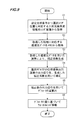
- FIG. 9 is a flowchart for explaining the operation after the AF instruction of the digital camera shown in FIG. 1 is given.
- a captured image signal obtained by imaging with the solid-state imaging device 5 at the time when the AF instruction is given is stored in the main memory 16. .
- system control unit 11 sets the position of the selected AF area 52 in the incident light beam angle information in the memory 3 corresponding to the optical condition of the lens apparatus 100 set when the AF instruction is given. Information on the corresponding incident ray angle is acquired (step S1).
- the system control unit 11 selects the incident ray angle information corresponding to the set optical condition.
- Information on incident light beam angles corresponding to the positions x 1 and x 2 at both ends of the AF area 52 is acquired from the memory 3.
- the system control unit 11 selects the selected AF from the incident ray angle information corresponding to the set optical condition. Information on incident light beam angles corresponding to the positions x 2 and x 3 at both ends of the area 52 is acquired from the memory 3.
- the system control unit 11 selects the incident ray angle information corresponding to the set optical condition. Information on incident light beam angles corresponding to the positions x3 and x4 at both ends of the AF area 52 is acquired from the memory 3.
- the system control unit 11 stores the sensitivity ratio data of the phase difference detection pixel 51R and the phase difference detection pixel 51L corresponding to each of the two incident ray angle information acquired in step S1 from the main memory 16. Obtain (step S2).
- step S2 the sensitivity ratio L1 of the phase difference detection pixel 51L corresponding to the position x1 and the position x1 are corresponded.
- Sensitivity ratio data is read from the main memory 16.
- the system control unit 11 generates a function indicating the sensitivity ratio of the phase difference detection pixel 51R and a function indicating the sensitivity ratio of the phase difference detection pixel 51L from the four sensitivity ratio data acquired in step S2.
- the phase difference detection pixel using the horizontal pixel position as a variable from the distance between x1 and x2 and the values of R1 and R2.
- a function of the sensitivity ratio of 51R (a function representing a straight line indicated by a two-point difference line in the drawing) can be generated.
- a function of the sensitivity ratio of the phase difference detection pixel 51L with the horizontal pixel position as a variable (a function representing a straight line indicated by a one-point difference line in the figure) ) Can be generated.
- the system control unit 11 For each horizontal pixel position where the phase difference pair in the selected AF area 52 exists, the system control unit 11 makes each phase difference pair have the same sensitivity ratio in the phase difference pair at the horizontal pixel position.
- a correction coefficient to be multiplied by is generated from the two functions generated as described above (step S3).
- the system control unit 11 acquires an output signal of each phase difference pair in the selected AF area 52 from the captured image signal stored in the main memory 16.
- the system control unit 11 corrects the output signal of each phase difference pair by multiplying the obtained output signal of each phase difference pair by the correction coefficient generated for the horizontal pixel position of each phase difference pair (step S4). .
- the system control unit 11 makes the phase difference pair in order to make the sensitivity ratio of the phase difference pair at the horizontal pixel position the same for each horizontal pixel position where the phase difference pair in the selected AF area 52 exists.
- a correction coefficient to be multiplied by one of the two may be generated from the two functions generated as described above, and only one output signal of the phase difference pair may be corrected in step S4 using the correction coefficient.
- the level difference is eliminated in the output signal of the phase difference pair at any horizontal pixel position in the selected AF area 52 by the correction process in step S4.
- the defocus amount calculation unit 19 calculates the phase difference amount by correlation calculation using the output signal of each corrected phase difference pair, and the defocus amount is calculated based on the calculated phase difference amount. Calculation is performed (step S5).
- the sensitivity ratio data corresponding to the incident light angle stored in the main memory 16 is obtained from the information on the incident light angle stored in the memory 3 of the lens device 100.
- the phase difference amount can be calculated after correcting the level difference of the output signal of the phase difference pair using the read and read sensitivity ratio data. Therefore, the calculation accuracy of the phase difference amount can be improved, and the phase difference AF can be performed with high accuracy.
- the correction coefficient can be generated by using the information on the incident light angle stored in the lens apparatus 100 and the internal table. Therefore, compared with the method of determining the level difference of the output signal of the phase difference pair from the captured image signal and generating the correction coefficient from the level difference, the time until the correction of the output signal of the phase difference pair is shortened The phase difference AF can be speeded up.
- the memory 3 of the lens apparatus 100 need only store information on the upper ray angle and the lower ray angle at an arbitrary horizontal pixel position. For this reason, the adjustment process before shipment of the lens apparatus 100 can be made sufficiently short, and the manufacturing cost of the lens apparatus 100 can be suppressed.
- the system control unit 11 creates two arbitrary positions (however, a phase difference) in the row direction X of the solid-state imaging device 5. Information on the incident ray angle at the position where the pair is placed is sufficient.
- the amount of information stored in the memory 3 of the lens apparatus 100 can be further reduced than the above-described example. In this case, it is only necessary to measure the incident light angle only at two positions in the row direction X. For this reason, the time required for generating the information stored in the memory 3 can also be shortened.
- FIG. 11 is a flowchart for explaining a modified example of the operation after the AF instruction of the digital camera shown in FIG. 1 is given.
- the same processes as those in FIG. 9 are denoted by the same reference numerals.
- a captured image signal obtained by imaging with the solid-state imaging device 5 at the time when the AF instruction is given is stored in the main memory 16.
- the system control unit 11 acquires the identification information (lens ID) of the lens device 100 stored in the memory 3 of the lens device 100 (step S10).
- the system control unit 11 then acquires the acquired lens ID, the optical conditions of the lens apparatus 100 when the AF instruction is given, and the position in the row direction X of the AF area 52 selected when the AF instruction is given. It is determined whether or not the correction coefficient for each phase difference pair is stored in the main memory 16 with respect to the combination with any one of the left end, the center, and the right end (step S11).
- step S11 If the correction coefficient is already stored (step S11: YES), the system control unit 11 acquires the stored correction coefficient from the main memory 16 in step S12, and selects the correction coefficient using the acquired correction coefficient. The output signal of the phase difference pair in the AF area 52 is corrected. After that, the process after step S5 is performed.
- step S11: NO the system control unit 11 performs the processing of step S1 to step S3.
- the system control unit 11 determines the correction coefficient generated in step S3, the lens ID acquired in step S10, the set optical condition, and the position of the selected AF area 52 in the row direction X. They are stored in the main memory 16 in association with each other (step S13). After step S13, the process after step S4 is performed.
- the system control unit 11 generates a correction coefficient for each phase difference pair for a combination of an arbitrary optical condition and an arbitrary AF area 52, and then the arbitrary optical condition is set and the AF area is set.
- 52 is selected and an AF instruction is issued, the output signal of the phase difference pair is corrected using the correction coefficient already generated and stored.
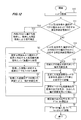
- FIG. 12 is a flowchart for explaining another modified example of the operation after the AF instruction of the digital camera shown in FIG. 1 is given.
- the same processes as those in FIG. 11 are denoted by the same reference numerals.
- step S11 determines the AF area 52 (hereinafter referred to as a symmetric area) that is in a line-symmetric relationship with the selected AF area 52 and the lens ID acquired in step S10. Then, it is determined whether or not a correction coefficient corresponding to the combination of the optical conditions of the lens apparatus 100 at the time when the AF instruction is given is stored in the main memory 16 (step S14).
- a correction coefficient corresponding to the combination of the optical conditions of the lens apparatus 100 at the time when the AF instruction is given is stored in the main memory 16 (step S14).
- the two AF areas 52 having a line-symmetrical relationship with respect to a straight line passing through the intersection with the optical axis on the light receiving surface 50 and extending in the column direction Y are referred to as line-symmetrical AF areas.
- step S14 When the correction coefficient is stored for the combination of the lens ID, the optical condition, and the symmetric area (step S14: YES), the system control unit 11 sets the correction coefficient for the combination of the lens ID, the optical condition, and the symmetric area. By using this, a correction coefficient for the currently set AF area 52 and optical conditions is generated (step S15). After step S15, the process after step S13 is performed.
- the sensitivity ratio line is in an inverted relationship.
- any one of the AF areas 52 from the optical axis position is arbitrarily selected.
- the correction coefficient for the phase difference detection pixel 51R (phase difference detection pixel 51L) at the horizontal pixel position at the distance is the phase difference at the horizontal pixel position at the arbitrary distance from the optical axis position in the other AF area 52. This is a correction coefficient for the detection pixel 51L (phase difference detection pixel 51R).
- step S1 If there is no AF area 52 that is line-symmetric with respect to the selected AF area 52, the system control unit 11 performs the processing from step S1 onward without performing the determination in step S14. In addition, when the determination in step S14 is NO, the system control unit 11 performs the processing after step S1.
- the system control unit 11 generates correction coefficients for each position of all the phase difference pairs included in the solid-state imaging device 5 from the sensitivity ratio function generated using the sensitivity ratio data acquired in step S2, This may be stored in the main memory 16 separately for each position of the AF area 52.
- the AF area 52 is provided on a part of the light receiving surface 50, but the AF area 52 may be set on the entire light receiving surface 50 without a gap.
- the pixels 51 are arranged in a so-called honeycomb arrangement, but the present invention can also be applied to a solid-state imaging device in which the pixels 51 are arranged in a square lattice.
- the solid-state image pickup device 5 is mounted with a plurality of color filters to perform color image pickup so far.
- the solid-state image pickup device 5 may be monochrome by omitting the color filter to be a single color of green or omitted.
- An imaging element for imaging may be used.
- a digital camera has been taken as an example of the imaging device, but the technology of the present embodiment can also be applied to a smartphone with a camera.
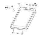
- FIG. 13 shows an appearance of a smartphone 200 that is an embodiment of the photographing apparatus of the present invention.
- a smartphone 200 illustrated in FIG. 13 includes a flat housing 201, and a display input in which a display panel 202 as a display unit and an operation panel 203 as an input unit are integrated on one surface of the housing 201. Part 204 is provided.
- Such a housing 201 includes a speaker 205, a microphone 206, an operation unit 207, and a camera unit 208.
- the configuration of the housing 201 is not limited thereto, and for example, a configuration in which the display unit and the input unit are independent can be employed, or a configuration having a folding structure and a slide mechanism can be employed.
- FIG. 14 is a block diagram showing a configuration of the smartphone 200 shown in FIG.
- the main components of the smartphone include a wireless communication unit 210, a display input unit 204, a call unit 211, an operation unit 207, a camera unit 208, a storage unit 212, and an external input / output unit. 213, a GPS (Global Positioning System) receiving unit 214, a motion sensor unit 215, a power supply unit 216, and a main control unit 220.
- a wireless communication function for performing mobile wireless communication via a base station device BS (not shown) and a mobile communication network NW (not shown) is provided.
- the wireless communication unit 210 performs wireless communication with the base station apparatus BS accommodated in the mobile communication network NW according to an instruction from the main control unit 220. Using this wireless communication, transmission and reception of various file data such as audio data and image data, e-mail data, and reception of Web data and streaming data are performed.
- the display input unit 204 displays images (still images and moving images), character information, and the like, visually transmits information to the user under the control of the main control unit 220, and detects user operations on the displayed information.
- a so-called touch panel which includes a display panel 202 and an operation panel 203.
- the display panel 202 uses an LCD (Liquid Crystal Display), an OELD (Organic Electro-Luminescence Display), or the like as a display device.
- LCD Liquid Crystal Display
- OELD Organic Electro-Luminescence Display
- the operation panel 203 is a device that is placed so that an image displayed on the display surface of the display panel 202 is visible and detects one or more coordinates operated by a user's finger or stylus.
- a detection signal generated due to the operation is output to the main control unit 220.
- the main control unit 220 detects an operation position (coordinates) on the display panel 202 based on the received detection signal.
- the display panel 202 and the operation panel 203 of the smartphone 200 exemplified as an embodiment of the photographing apparatus of the present invention integrally constitute a display input unit 204.
- the arrangement 203 covers the display panel 202 completely.
- the operation panel 203 may have a function of detecting a user operation even in an area outside the display panel 202.
- the operation panel 203 includes a detection area (hereinafter referred to as a display area) for an overlapping portion that overlaps the display panel 202 and a detection area (hereinafter, a non-display area) for an outer edge portion that does not overlap the other display panel 202. May be included).
- the operation panel 203 may include two sensitive areas of the outer edge portion and the other inner portion. Further, the width of the outer edge portion is appropriately designed according to the size of the housing 201 and the like.
- the position detection method employed in the operation panel 203 include a matrix switch method, a resistance film method, a surface acoustic wave method, an infrared method, an electromagnetic induction method, a capacitance method, and the like. You can also
- the call unit 211 includes a speaker 205 and a microphone 206, converts user's voice input through the microphone 206 into voice data that can be processed by the main control unit 220, and outputs the voice data to the main control unit 220. 210 or the audio data received by the external input / output unit 213 is decoded and output from the speaker 205.
- the speaker 205 can be mounted on the same surface as the surface on which the display input unit 204 is provided, and the microphone 206 can be mounted on the side surface of the housing 201.
- the operation unit 207 is a hardware key using a key switch or the like, and receives an instruction from the user.
- the operation unit 207 is mounted on the side surface of the housing 201 of the smartphone 200 and is turned on when pressed with a finger or the like, and turned off when the finger is released with a restoring force such as a spring. It is a push button type switch.
- the storage unit 212 includes a control program and control data of the main control unit 220, application software, address data that associates the name and telephone number of a communication partner, transmitted / received e-mail data, Web data downloaded by Web browsing, The downloaded content data is stored, and streaming data and the like are temporarily stored.
- the storage unit 212 includes an internal storage unit 217 built in the smartphone and an external storage unit 218 having a removable external memory slot.
- Each of the internal storage unit 217 and the external storage unit 218 constituting the storage unit 212 includes a flash memory type (hard memory type), a hard disk type (hard disk type), a multimedia card micro type (multimedia card micro type), This is realized using a storage medium such as a card type memory (for example, MicroSD (registered trademark) memory), a RAM (Random Access Memory), a ROM (Read Only Memory), or the like.
- a flash memory type hard memory type
- hard disk type hard disk type
- multimedia card micro type multimedia card micro type
- a storage medium such as a card type memory (for example, MicroSD (registered trademark) memory), a RAM (Random Access Memory), a ROM (Read Only Memory), or the like.
- the external input / output unit 213 serves as an interface with all external devices connected to the smartphone 200, and communicates with other external devices (for example, universal serial bus (USB), IEEE 1394, etc.) or a network.
- external devices for example, universal serial bus (USB), IEEE 1394, etc.
- a network for example, the Internet, wireless LAN, Bluetooth (registered trademark), RFID (Radio Frequency Identification), Infrared Data Association (IrDA) (registered trademark), UWB (Ultra Wideband) (registered trademark) ZigBee) (registered trademark, etc.) for direct or indirect connection.
- an external device connected to the smartphone 200 for example, a wired / wireless headset, a wired / wireless external charger, a wired / wireless data port, a memory card (Memory card) connected via a card socket, or a SIM (Subscriber).
- Identity Module Card / UIM (User Identity Module Card) card external audio / video equipment connected via audio / video I / O (Input / Output) terminal, external audio / video equipment connected wirelessly, yes / no
- the external input / output unit 213 transmits data received from such an external device to each component inside the smartphone 200, or allows the data inside the smartphone 200 to be transmitted to the external device. Can do.
- the GPS receiving unit 214 receives GPS signals transmitted from the GPS satellites ST1 to STn in accordance with instructions from the main control unit 220, executes positioning calculation processing based on the received GPS signals, and calculates the latitude of the smartphone 200 Detect the position consisting of longitude and altitude.
- the GPS reception unit 214 can acquire position information from the wireless communication unit 210 or the external input / output unit 213 (for example, a wireless LAN), the GPS reception unit 214 can also detect the position using the position information.
- the motion sensor unit 215 includes, for example, a three-axis acceleration sensor, and detects the physical movement of the smartphone 200 in accordance with an instruction from the main control unit 220. By detecting the physical movement of the smartphone 200, the moving direction and acceleration of the smartphone 200 are detected. The detection result is output to the main control unit 220.
- the power supply unit 216 supplies power stored in a battery (not shown) to each unit of the smartphone 200 in accordance with an instruction from the main control unit 220.
- the main control unit 220 includes a microprocessor, operates according to a control program and control data stored in the storage unit 212, and controls each unit of the smartphone 200 in an integrated manner.
- the main control unit 220 includes a mobile communication control function that controls each unit of the communication system and an application processing function in order to perform voice communication and data communication through the wireless communication unit 210.
- the application processing function is realized by the main control unit 220 operating according to the application software stored in the storage unit 212.
- Examples of the application processing function include an infrared communication function for controlling the external input / output unit 213 to perform data communication with the opposite device, an e-mail function for transmitting / receiving e-mails, and a web browsing function for browsing web pages. .
- the main control unit 220 has an image processing function such as displaying video on the display input unit 204 based on image data (still image or moving image data) such as received data or downloaded streaming data.
- the image processing function is a function in which the main control unit 220 decodes the image data, performs image processing on the decoding result, and displays an image on the display input unit 204.
- the main control unit 220 executes display control for the display panel 202 and operation detection control for detecting a user operation through the operation unit 207 and the operation panel 203.
- the main control unit 220 displays an icon for starting application software, a software key such as a scroll bar, or a window for creating an e-mail.
- a software key such as a scroll bar, or a window for creating an e-mail.
- the scroll bar refers to a software key for accepting an instruction to move the display portion of a large image that does not fit in the display area of the display panel 202.
- the main control unit 220 detects a user operation through the operation unit 207 or accepts an operation on the icon or an input of a character string in the input field of the window through the operation panel 203. Or a display image scroll request through a scroll bar.
- the main control unit 220 causes the operation position with respect to the operation panel 203 to overlap with the display panel 202 (display area) or other outer edge part (non-display area) that does not overlap with the display panel 202.
- a touch panel control function for controlling the sensitive area of the operation panel 203 and the display position of the software key.
- the main control unit 220 can also detect a gesture operation on the operation panel 203 and execute a preset function in accordance with the detected gesture operation.
- Gesture operation is not a conventional simple touch operation, but an operation that draws a trajectory with a finger or the like, designates a plurality of positions at the same time, or combines these to draw a trajectory for at least one of a plurality of positions. means.
- the camera unit 208 includes configurations other than the external memory control unit 20, the recording medium 21, the display control unit 22, the display unit 23, and the operation unit 14 in the camera main body 200 illustrated in FIG.
- the captured image data generated by the camera unit 208 can be recorded in the storage unit 212 or output through the input / output unit 213 or the wireless communication unit 210.
- the camera unit 208 is mounted on the same surface as the display input unit 204, but the mounting position of the camera unit 208 is not limited to this, and the camera unit 208 may be mounted on the back surface of the display input unit 204. Good.
- the camera unit 208 can be used for various functions of the smartphone 200.
- an image acquired by the camera unit 208 can be displayed on the display panel 202, or the image of the camera unit 208 can be used as one of operation inputs of the operation panel 203.
- the GPS receiving unit 214 detects a position
- the position can be detected with reference to an image from the camera unit 208.
- the optical axis direction of the camera unit 208 of the smartphone 200 is determined without using the triaxial acceleration sensor or in combination with the triaxial acceleration sensor. It is also possible to determine the current usage environment.
- the image from the camera unit 208 can also be used in the application software.
- the position information acquired by the GPS receiver 214 to the image data of the still image or the moving image, the voice information acquired by the microphone 206 (the text information may be converted into voice information by the main control unit or the like), Posture information and the like acquired by the motion sensor unit 215 can be added and recorded in the recording unit 212, or output through the input / output unit 213 and the wireless communication unit 210.
- the solid-state imaging device 5 is used as the imaging device of the camera unit 208, the lens device 100 can be mounted, and the camera unit 208 performs the processing illustrated in FIGS.
- the camera unit 208 performs the processing illustrated in FIGS.
- the disclosed imaging apparatus is an imaging apparatus in which an imaging optical system is detachable, and includes a plurality of imaging pixels that capture an image formed by a light beam that has passed through a pupil region of the imaging optical system, and the imaging optical system.
- a plurality of first phase difference detection pixels that capture one of a pair of images formed by a pair of light beams that have passed through different parts of the pupil region, and a plurality of second positions that capture the other of the pair of images
- the imaging element including the light receiving surface on which the phase difference detection pixels are arranged, and the information on the different incident light beam angles at arbitrary positions in the shift direction of the pair of images on the light receiving surface, the first position at the arbitrary position.
- the sensitivity ratio between one phase difference detection pixel and the imaging pixel adjacent thereto, and the sensitivity between the second phase difference detection pixel located at the arbitrary position and the imaging pixel adjacent thereto The first to store sensitivity ratio data indicating the ratio
- a storage section and the imaging optical system stores information on incident light beam angles of rays incident through the imaging optical system at each of at least two positions in the shift direction of the light receiving surface.
- a second storage unit for storing each optical condition of the optical system is provided, and information on the incident light angle at the at least two positions corresponding to the set optical condition is acquired from the second storage unit, Using the sensitivity ratio data stored in the first storage unit corresponding to each of the acquired plurality of incident light beam angle information, the first phase difference detection pixel and the pixel are arranged in proximity to the first phase difference detection pixel.
- a correction unit that corrects a level difference between output signals of the second pair of phase difference detection pixels, and a defocus amount calculation unit that calculates a defocus amount using the corrected output signals of the pair And further comprising Than is.
- the position in the shift direction is calculated by the correction unit using the sensitivity ratio data corresponding to each of the two pieces of incident light angle information acquired from the second storage unit. For each of the same pair, a correction coefficient that multiplies at least one output signal of the pair necessary to correct the level difference between the output signals of the pair is generated, and the generated correction coefficient is used as at least one output signal of the pair. To correct the level difference between the pair of output signals.
- a plurality of phase difference detection areas which are target areas for phase difference detection including the plurality of pairs arranged in the shift direction, are arranged in the shift direction on the light receiving surface, and the correction unit
- the position in the shift direction in the phase difference detection area selected by the calculation using the sensitivity ratio data corresponding to each of the two pieces of information on the incident light angle acquired from the second storage unit is the same.
- the correction coefficient is generated for each pair, and the correction is performed by multiplying the generated correction coefficient by at least one output signal of the pair in the selected phase difference detection area.
- the correction unit includes two phase differences that are in line symmetry with respect to a straight line passing through an intersection with the optical axis of the imaging optical system on the light receiving surface and orthogonal to the shift direction. For one of the detection areas, a new correction coefficient is generated from the correction coefficient generated for the other of the two phase difference detection areas.
- the correction unit generates the correction coefficient generated for each pair of the phase difference detection areas in a state where the arbitrary optical conditions are set and the arbitrary phase difference detection area is selected. Then, when the arbitrary optical condition is set and the phase difference detection area is selected, the correction is performed using the stored correction coefficient.
- information on an incident light beam angle at an arbitrary position on the light receiving surface causes the imaging optical system and the imaging element to be orthogonal to the shift direction and light of a lens included in the imaging optical system.
- an angle formed by an upper light beam that passes through one end in the shifting direction of the lens and reaches the arbitrary position, and the optical axis of the lens is information indicating an angle formed by a lower light beam that passes through the other end portion of the lens in the shift direction and reaches the arbitrary position and an optical axis of the lens.
- the disclosed imaging optical system is the imaging optical system in the imaging apparatus, and can be attached to an imaging apparatus having a mount mechanism.
- the disclosed defocus amount calculation method is a defocus amount calculation method by an image pickup device to which an image pickup optical system can be attached and detached, and the image pickup device is an image formed by a light beam that has passed through a pupil region of the image pickup optical system.
- An image pickup device including a light receiving surface on which a plurality of second phase difference detection pixels for picking up the other of the pair of images is disposed, and different incident light rays at arbitrary positions in the shift direction of the pair of images on the light receiving surface.
- a first storage unit that stores sensitivity ratio data indicating a sensitivity ratio with respect to the imaging pixels, and the imaging optical system includes the imaging optical system at each of at least two positions in the shift direction of the light receiving surface.
- a second storage unit is provided for storing information on the incident ray angle of the light ray incident through the imaging optical system for each optical condition of the imaging optical system, and the at least two corresponding to the set optical conditions are provided.
- the information on the incident ray angle at the position is acquired from the second storage unit, and the sensitivity ratio data stored in the first storage unit corresponding to each of the acquired information on the incident ray angle is obtained.
- the present invention is useful when applied to a digital camera.
- Solid-state image sensor 11
- System control unit (correction unit) 19
- Defocus amount calculation unit 50
- Light receiving surface 51 Pixel 52
- AF area (phase difference detection area) 51R
- 51L Phase difference detection pixel X Row direction shift direction of a pair of images
- Y row direction K optical axis
Landscapes
- Physics & Mathematics (AREA)
- Engineering & Computer Science (AREA)
- Multimedia (AREA)
- Signal Processing (AREA)
- General Physics & Mathematics (AREA)
- Optics & Photonics (AREA)
- Spectroscopy & Molecular Physics (AREA)
- Studio Devices (AREA)
- Focusing (AREA)
- Automatic Focus Adjustment (AREA)
- Structure And Mechanism Of Cameras (AREA)
Abstract
Description
本出願は、2012年11月22日出願の日本特許出願(特願2012-256349)に基づくものであり、その内容はここに取り込まれる。
11 システム制御部(補正部)
19 デフォーカス量演算部
50 受光面
51 画素
52 AFエリア(位相差検出エリア)
51R,51L 位相差検出用画素
X 行方向(一対の像のずれ方向)
Y 列方向
K 光軸
Claims (8)
- 撮像光学系を着脱可能な撮像装置であって、
前記撮像光学系の瞳領域を通過した光束により形成された像を撮像する複数の撮像用画素、前記撮像光学系の瞳領域の異なる部分を通過した一対の光束により形成された一対の像の一方を撮像する複数の第一の位相差検出用画素、及び前記一対の像の他方を撮像する複数の第二の位相差検出用画素が配置される受光面を含む撮像素子と、
前記受光面の前記一対の像のずれ方向での任意の位置における異なる入射光線角度の情報毎に、当該任意の位置にある前記第一の位相差検出用画素とこれに近接する前記撮像用画素との感度比、及び、当該任意の位置にある前記第二の位相差検出用画素とこれに近接する前記撮像用画素との感度比を示す感度比データを記憶する第一の記憶部と、を備え、
前記撮像光学系には、前記受光面の前記ずれ方向での少なくとも2つの位置の各々における前記撮像光学系を介して入射する光線の入射光線角度の情報を、前記撮像光学系の光学条件毎に記憶する第二の記憶部が設けられ、
設定された前記光学条件に対応する前記少なくとも2つの位置における前記入射光線角度の情報を前記第二の記憶部から取得し、取得した複数の前記入射光線角度の情報の各々に対応する前記第一の記憶部に記憶されている前記感度比データを用いて、前記第一の位相差検出用画素とこれに近接して配置される前記第二の位相差検出用画素のペアの出力信号のレベル差を補正する補正部と、
前記補正後の前記ペアの出力信号を利用してデフォーカス量を演算するデフォーカス量演算部とを更に備える撮像装置。 - 請求項1記載の撮像装置であって、
前記補正部は、前記第二の記憶部から取得した2つの前記入射光線角度の情報の各々に対応する前記感度比データを用いた演算により、前記ずれ方向における位置が同じ前記ペア毎に、当該ペアの出力信号のレベル差を補正するために必要な前記ペアの少なくとも一方の出力信号に乗じる補正係数を生成し、生成した補正係数を前記ペアの少なくとも一方の出力信号に乗じて、前記ペアの出力信号のレベル差を補正する撮像装置。 - 請求項2記載の撮像装置であって、
前記受光面には、前記ずれ方向に並ぶ複数の前記ペアを含む位相差検出の対象エリアである位相差検出エリアが前記ずれ方向に複数並べて設けられ、
前記補正部は、前記第二の記憶部から取得した2つの前記入射光線角度の情報の各々に対応する前記感度比データを用いた演算により、選択された前記位相差検出エリアでの前記ずれ方向における位置が同じ前記ペア毎に前記補正係数を生成し、生成した補正係数を、前記選択された位相差検出エリアにある前記ペアの少なくとも一方の出力信号に乗じて前記補正を行う撮像装置。 - 請求項3記載の撮像装置であって、
前記補正部は、前記受光面における前記撮像光学系の光軸との交点を通りかつ前記ずれ方向に直交する直線を軸として線対称の関係にある2つの前記位相差検出エリアの一方については、当該2つの位相差検出エリアの他方について生成した前記補正係数から、新たな前記補正係数を生成する撮像装置。 - 請求項3記載の撮像装置であって、
前記補正部は、任意の前記光学条件が設定されかつ任意の前記位相差検出エリアが選択された状態で当該位相差検出エリアの前記ペア毎に生成した前記補正係数を記憶し、その後、当該任意の光学条件が設定されかつ当該位相差検出エリアが選択された場合には、前記記憶した補正係数を利用して前記補正を行う撮像装置。 - 請求項1乃至5のいずれか1項記載の撮像装置であって、
前記受光面上の任意の位置における入射光線角度の情報は、前記撮像光学系及び前記撮像素子を、前記ずれ方向に直交しかつ前記撮像光学系に含まれるレンズの光軸に直交する方向から見たときの、前記レンズの前記ずれ方向における一方の端部を通り前記任意の位置に到達する光線である上光線と前記レンズの光軸とのなす角度、及び、前記レンズの前記ずれ方向における他方の端部を通り前記任意の位置に到達する光線である下光線と前記レンズの光軸とのなす角度、を示す情報である撮像装置。 - 請求項1記載の撮像装置における前記撮像光学系であって、
マウント機構を有する撮像装置に装着可能である撮像光学系。 - 撮像光学系を着脱可能な撮像装置によるデフォーカス量演算方法であって、
前記撮像装置は、
前記撮像光学系の瞳領域を通過した光束により形成された像を撮像する複数の撮像用画素、前記撮像光学系の瞳領域の異なる部分を通過した一対の光束により形成された一対の像の一方を撮像する複数の第一の位相差検出用画素、及び前記一対の像の他方を撮像する複数の第二の位相差検出用画素が配置される受光面を含む撮像素子と、
前記受光面の前記一対の像のずれ方向での任意の位置における異なる入射光線角度の情報毎に、当該任意の位置にある前記第一の位相差検出用画素とこれに近接する前記撮像用画素との感度比、及び、当該任意の位置にある前記第二の位相差検出用画素とこれに近接する前記撮像用画素との感度比を示す感度比データを記憶する第一の記憶部と、を備え、
前記撮像光学系には、前記受光面の前記ずれ方向での少なくとも2つの位置の各々における前記撮像光学系を介して入射する光線の入射光線角度の情報を、前記撮像光学系の光学条件毎に記憶する第二の記憶部が設けられ、
設定された前記光学条件に対応する前記少なくとも2つの位置における前記入射光線角度の情報を前記第二の記憶部から取得し、取得した複数の前記入射光線角度の情報の各々に対応する前記第一の記憶部に記憶されている前記感度比データを用いて、前記第一の位相差検出用画素とこれに近接して配置される前記第二の位相差検出用画素のペアの出力信号のレベル差を補正する補正ステップと、
前記補正後の前記ペアの出力信号を利用してデフォーカス量を演算するデフォーカス量演算ステップとを備えるデフォーカス量演算方法。
Priority Applications (4)
| Application Number | Priority Date | Filing Date | Title |
|---|---|---|---|
| DE112013005594.5T DE112013005594T5 (de) | 2012-11-22 | 2013-08-30 | Abbildungsvorrichtung, Unschärfebetrag-Berechnungsverfahren und Objektivvorrichtung |
| CN201380061181.2A CN104854496B (zh) | 2012-11-22 | 2013-08-30 | 摄像装置、散焦量运算方法及摄像光学系统 |
| JP2014548481A JP5775976B2 (ja) | 2012-11-22 | 2013-08-30 | 撮像装置、デフォーカス量演算方法、及び撮像光学系 |
| US14/709,653 US9386216B2 (en) | 2012-11-22 | 2015-05-12 | Imaging device, defocus amount calculating method, and imaging optical system |
Applications Claiming Priority (2)
| Application Number | Priority Date | Filing Date | Title |
|---|---|---|---|
| JP2012256349 | 2012-11-22 | ||
| JP2012-256349 | 2012-11-22 |
Related Child Applications (1)
| Application Number | Title | Priority Date | Filing Date |
|---|---|---|---|
| US14/709,653 Continuation US9386216B2 (en) | 2012-11-22 | 2015-05-12 | Imaging device, defocus amount calculating method, and imaging optical system |
Publications (1)
| Publication Number | Publication Date |
|---|---|
| WO2014080674A1 true WO2014080674A1 (ja) | 2014-05-30 |
Family
ID=50775865
Family Applications (1)
| Application Number | Title | Priority Date | Filing Date |
|---|---|---|---|
| PCT/JP2013/073391 Ceased WO2014080674A1 (ja) | 2012-11-22 | 2013-08-30 | 撮像装置、デフォーカス量演算方法、及び撮像光学系 |
Country Status (5)
| Country | Link |
|---|---|
| US (1) | US9386216B2 (ja) |
| JP (1) | JP5775976B2 (ja) |
| CN (1) | CN104854496B (ja) |
| DE (1) | DE112013005594T5 (ja) |
| WO (1) | WO2014080674A1 (ja) |
Cited By (4)
| Publication number | Priority date | Publication date | Assignee | Title |
|---|---|---|---|---|
| JP2015018256A (ja) * | 2013-01-10 | 2015-01-29 | オリンパスイメージング株式会社 | 撮像装置及び光軸位置算出方法 |
| JP2015072357A (ja) * | 2013-10-02 | 2015-04-16 | オリンパス株式会社 | 焦点調節装置 |
| EP2993506A1 (en) * | 2014-09-05 | 2016-03-09 | Canon Kabushiki Kaisha | Interchangeable lens apparatus, image capturing apparatus and focusing program |
| WO2016035566A1 (ja) * | 2014-09-01 | 2016-03-10 | ソニー株式会社 | 固体撮像素子及びその信号処理方法、並びに電子機器 |
Families Citing this family (16)
| Publication number | Priority date | Publication date | Assignee | Title |
|---|---|---|---|---|
| JP5746794B2 (ja) * | 2012-09-27 | 2015-07-08 | 富士フイルム株式会社 | 撮像装置及び画像処理方法 |
| JP5777825B2 (ja) * | 2012-12-05 | 2015-09-09 | 富士フイルム株式会社 | 撮像装置、異常斜め入射光検出方法及びプログラム、並びに記録媒体 |
| WO2014087804A1 (ja) * | 2012-12-07 | 2014-06-12 | 富士フイルム株式会社 | 撮像装置、画像処理方法及びプログラム |
| JP5802858B2 (ja) * | 2013-03-05 | 2015-11-04 | 富士フイルム株式会社 | 撮像装置、画像処理装置、画像処理方法及びプログラム |
| JP5865555B2 (ja) * | 2013-05-13 | 2016-02-17 | 富士フイルム株式会社 | 混色率算出装置及び方法並びに撮像装置 |
| JP5775918B2 (ja) * | 2013-09-27 | 2015-09-09 | オリンパス株式会社 | 撮像装置、画像処理方法及び画像処理プログラム |
| JP6021780B2 (ja) * | 2013-10-07 | 2016-11-09 | キヤノン株式会社 | 画像データ処理装置、距離算出装置、撮像装置および画像データ処理方法 |
| JP6849325B2 (ja) * | 2016-06-10 | 2021-03-24 | キヤノン株式会社 | 制御装置、撮像装置、制御方法、プログラム、および、記憶媒体 |
| JP6881911B2 (ja) | 2016-08-01 | 2021-06-02 | キヤノン株式会社 | 制御装置、撮像装置、制御方法、プログラム、および、記憶媒体 |
| JP6911136B2 (ja) | 2017-09-28 | 2021-07-28 | 富士フイルム株式会社 | 撮像装置、情報取得方法及び情報取得プログラム |
| CN111201780B (zh) * | 2017-10-19 | 2022-09-16 | 索尼公司 | 成像装置和方法以及图像处理装置和方法 |
| EP3700192B1 (en) * | 2017-10-19 | 2023-08-30 | Sony Group Corporation | Imaging device and signal processing device |
| US11641519B2 (en) * | 2018-07-20 | 2023-05-02 | Nikon Corporation | Focus detection device, imaging device, and interchangeable lens |
| US11172142B2 (en) * | 2018-09-25 | 2021-11-09 | Taiwan Semiconductor Manufacturing Co., Ltd. | Image sensor for sensing LED light with reduced flickering |
| JP7271159B2 (ja) * | 2018-12-14 | 2023-05-11 | キヤノン株式会社 | 制御装置、撮像装置、レンズ装置、プログラム、および制御装置の制御方法 |
| CN113232677A (zh) * | 2021-05-10 | 2021-08-10 | 前海七剑科技(深圳)有限公司 | 车辆驾驶辅助控制方法、控制系统、电子设备及存储介质 |
Citations (3)
| Publication number | Priority date | Publication date | Assignee | Title |
|---|---|---|---|---|
| JPH05333263A (ja) * | 1992-05-29 | 1993-12-17 | Canon Inc | 合焦検出装置及びカメラの自動焦点調節装置 |
| JP2011164370A (ja) * | 2010-02-10 | 2011-08-25 | Nikon Corp | 焦点検出装置 |
| JP2012004729A (ja) * | 2010-06-15 | 2012-01-05 | Fujifilm Corp | 撮像装置及び画像処理方法 |
Family Cites Families (33)
| Publication number | Priority date | Publication date | Assignee | Title |
|---|---|---|---|---|
| JP2005341033A (ja) * | 2004-05-25 | 2005-12-08 | Konica Minolta Photo Imaging Inc | 撮像装置及びプログラム |
| JP4931225B2 (ja) | 2007-04-26 | 2012-05-16 | キヤノン株式会社 | 撮像装置 |
| JP5219865B2 (ja) * | 2008-02-13 | 2013-06-26 | キヤノン株式会社 | 撮像装置及び焦点制御方法 |
| JP2010008873A (ja) * | 2008-06-30 | 2010-01-14 | Nikon Corp | 焦点検出装置および撮像装置 |
| JP5164707B2 (ja) | 2008-07-17 | 2013-03-21 | キヤノン株式会社 | 位相差検出装置、撮像装置、位相差検出装置の信号レベル補正方法、信号レベル補正プログラム |
| JP5300414B2 (ja) | 2008-10-30 | 2013-09-25 | キヤノン株式会社 | カメラ及びカメラシステム |
| JP5147645B2 (ja) * | 2008-10-30 | 2013-02-20 | キヤノン株式会社 | 撮像装置 |
| JP2011059337A (ja) * | 2009-09-09 | 2011-03-24 | Fujifilm Corp | 撮像装置 |
| JP2011176715A (ja) * | 2010-02-25 | 2011-09-08 | Nikon Corp | 裏面照射型撮像素子および撮像装置 |
| JP2011221254A (ja) * | 2010-04-08 | 2011-11-04 | Sony Corp | 撮像装置、固体撮像素子、撮像方法およびプログラム |
| JP5764884B2 (ja) * | 2010-08-16 | 2015-08-19 | ソニー株式会社 | 撮像素子および撮像装置 |
| JP5468178B2 (ja) * | 2011-03-31 | 2014-04-09 | 富士フイルム株式会社 | 撮像装置、撮像装置の制御方法及びプログラム |
| CN103460103B (zh) * | 2011-03-31 | 2015-06-17 | 富士胶片株式会社 | 成像装置及其驱动方法 |
| KR101773168B1 (ko) * | 2011-07-21 | 2017-09-12 | 삼성전자주식회사 | 위상차이 촬상 소자에 의한 초점 조절 장치 및 방법 |
| JP6000520B2 (ja) * | 2011-07-25 | 2016-09-28 | キヤノン株式会社 | 撮像装置およびその制御方法およびプログラム |
| EP2762944B1 (en) * | 2011-09-28 | 2016-11-23 | Fujifilm Corporation | Imaging device and focusing control method |
| WO2013046973A1 (ja) * | 2011-09-29 | 2013-04-04 | 富士フイルム株式会社 | 固体撮像素子、撮像装置、及び合焦制御方法 |
| WO2013047110A1 (ja) * | 2011-09-30 | 2013-04-04 | 富士フイルム株式会社 | 撮像装置及び位相差画素の感度比算出方法 |
| EP2762941B1 (en) * | 2011-09-30 | 2016-12-28 | Fujifilm Corporation | Imaging device and focus parameter value calculation method |
| JP5911252B2 (ja) * | 2011-09-30 | 2016-04-27 | キヤノン株式会社 | 撮像装置及び画像処理方法 |
| JP5943655B2 (ja) * | 2012-03-12 | 2016-07-05 | キヤノン株式会社 | 画像処理装置、焦点検出装置、および、画像処理プログラム |
| JP5690974B2 (ja) * | 2012-05-01 | 2015-03-25 | 富士フイルム株式会社 | 撮像装置及び合焦制御方法 |
| JP5529928B2 (ja) * | 2012-06-14 | 2014-06-25 | オリンパスイメージング株式会社 | 撮像装置及び撮像装置の制御方法 |
| WO2013190899A1 (ja) * | 2012-06-19 | 2013-12-27 | 富士フイルム株式会社 | 撮像装置及び自動焦点調節方法 |
| JP5750550B2 (ja) * | 2012-09-06 | 2015-07-22 | 富士フイルム株式会社 | 撮像装置及び合焦制御方法 |
| JP2014056002A (ja) * | 2012-09-11 | 2014-03-27 | Sony Corp | 焦点検出装置、撮像装置、および、焦点検出装置の制御方法 |
| JP6149369B2 (ja) * | 2012-09-27 | 2017-06-21 | 株式会社ニコン | 撮像素子 |
| CN104813648B (zh) * | 2012-12-11 | 2018-06-05 | 富士胶片株式会社 | 图像处理装置、摄像装置、及图像处理方法 |
| JP5635584B2 (ja) * | 2012-12-20 | 2014-12-03 | オリンパスイメージング株式会社 | 撮影機器、カメラシステム及びフォーカス制御のための情報を算出する方法 |
| JP6045362B2 (ja) * | 2013-01-17 | 2016-12-14 | オリンパス株式会社 | 撮像装置および焦点検出方法 |
| WO2014141561A1 (ja) * | 2013-03-13 | 2014-09-18 | 富士フイルム株式会社 | 撮像装置、信号処理方法、信号処理プログラム |
| JP6186900B2 (ja) * | 2013-06-04 | 2017-08-30 | ソニー株式会社 | 固体撮像装置、電子機器、レンズ制御方法、および撮像モジュール |
| JP6124720B2 (ja) * | 2013-07-22 | 2017-05-10 | オリンパス株式会社 | 撮像装置、画像処理方法及び画像処理プログラム |
-
2013
- 2013-08-30 JP JP2014548481A patent/JP5775976B2/ja not_active Expired - Fee Related
- 2013-08-30 CN CN201380061181.2A patent/CN104854496B/zh not_active Expired - Fee Related
- 2013-08-30 WO PCT/JP2013/073391 patent/WO2014080674A1/ja not_active Ceased
- 2013-08-30 DE DE112013005594.5T patent/DE112013005594T5/de not_active Withdrawn
-
2015
- 2015-05-12 US US14/709,653 patent/US9386216B2/en not_active Expired - Fee Related
Patent Citations (3)
| Publication number | Priority date | Publication date | Assignee | Title |
|---|---|---|---|---|
| JPH05333263A (ja) * | 1992-05-29 | 1993-12-17 | Canon Inc | 合焦検出装置及びカメラの自動焦点調節装置 |
| JP2011164370A (ja) * | 2010-02-10 | 2011-08-25 | Nikon Corp | 焦点検出装置 |
| JP2012004729A (ja) * | 2010-06-15 | 2012-01-05 | Fujifilm Corp | 撮像装置及び画像処理方法 |
Cited By (13)
| Publication number | Priority date | Publication date | Assignee | Title |
|---|---|---|---|---|
| JP2015018256A (ja) * | 2013-01-10 | 2015-01-29 | オリンパスイメージング株式会社 | 撮像装置及び光軸位置算出方法 |
| US9398207B2 (en) | 2013-01-10 | 2016-07-19 | Olympus Corporation | Imaging apparatus and image correction method, and image processing apparatus and image processing method |
| JP2015072357A (ja) * | 2013-10-02 | 2015-04-16 | オリンパス株式会社 | 焦点調節装置 |
| CN105580352A (zh) * | 2014-09-01 | 2016-05-11 | 索尼公司 | 固体摄像器件、固体摄像器件的信号处理方法和电子装置 |
| JP2016052041A (ja) * | 2014-09-01 | 2016-04-11 | ソニー株式会社 | 固体撮像素子及びその信号処理方法、並びに電子機器 |
| WO2016035566A1 (ja) * | 2014-09-01 | 2016-03-10 | ソニー株式会社 | 固体撮像素子及びその信号処理方法、並びに電子機器 |
| US9918031B2 (en) | 2014-09-01 | 2018-03-13 | Sony Corporation | Solid-state imaging device and electronic apparatus having a pixel unit with one microlens and a correction circuit |
| CN105580352B (zh) * | 2014-09-01 | 2020-01-14 | 索尼公司 | 固体摄像器件、固体摄像器件的信号处理方法和电子装置 |
| US10542229B2 (en) | 2014-09-01 | 2020-01-21 | Sony Corporation | Solid-state imaging device, signal processing method therefor, and electronic apparatus for enabling sensitivity correction |
| US11770639B2 (en) | 2014-09-01 | 2023-09-26 | Sony Group Corporation | Solid-state imaging device, signal processing method therefor, and electronic apparatus for enabling sensitivity correction |
| CN105407265A (zh) * | 2014-09-05 | 2016-03-16 | 佳能株式会社 | 可互换透镜装置、图像捕获装置和控制方法 |
| EP2993506A1 (en) * | 2014-09-05 | 2016-03-09 | Canon Kabushiki Kaisha | Interchangeable lens apparatus, image capturing apparatus and focusing program |
| US10244157B2 (en) | 2014-09-05 | 2019-03-26 | Canon Kabushiki Kaisha | Interchangeable lens apparatus and image capturing apparatus capable of acquiring in-focus state at different image heights, and storage medium storing focusing program |
Also Published As
| Publication number | Publication date |
|---|---|
| CN104854496A (zh) | 2015-08-19 |
| US20150244926A1 (en) | 2015-08-27 |
| JP5775976B2 (ja) | 2015-09-09 |
| DE112013005594T5 (de) | 2015-10-22 |
| US9386216B2 (en) | 2016-07-05 |
| CN104854496B (zh) | 2017-04-12 |
| JPWO2014080674A1 (ja) | 2017-01-05 |
Similar Documents
| Publication | Publication Date | Title |
|---|---|---|
| JP5775976B2 (ja) | 撮像装置、デフォーカス量演算方法、及び撮像光学系 | |
| JP5542249B2 (ja) | 撮像素子及びこれを用いた撮像装置及び撮像方法 | |
| JP6031587B2 (ja) | 撮像装置、信号処理方法、信号処理プログラム | |
| JP5690974B2 (ja) | 撮像装置及び合焦制御方法 | |
| JP5799178B2 (ja) | 撮像装置及び合焦制御方法 | |
| JP5779726B2 (ja) | 撮像装置及び露出決定方法 | |
| JP5948492B2 (ja) | 撮像装置及び合焦制御方法 | |
| JP5750550B2 (ja) | 撮像装置及び合焦制御方法 | |
| JP5934843B2 (ja) | 撮像装置及び合焦制御方法 | |
| JP5978411B2 (ja) | 撮像装置及び合焦制御方法 | |
| WO2015118727A1 (ja) | 撮像装置及び合焦制御方法 | |
| JP5542248B2 (ja) | 撮像素子及び撮像装置 | |
| JP5982600B2 (ja) | 撮像装置及び合焦制御方法 | |
| WO2015146229A1 (ja) | 撮像装置及び合焦制御方法 | |
| WO2014065004A1 (ja) | 撮像装置及びその合焦制御方法 | |
| JP5677628B2 (ja) | 撮像装置及び撮像方法 |
Legal Events
| Date | Code | Title | Description |
|---|---|---|---|
| 121 | Ep: the epo has been informed by wipo that ep was designated in this application |
Ref document number: 13856873 Country of ref document: EP Kind code of ref document: A1 |
|
| ENP | Entry into the national phase |
Ref document number: 2014548481 Country of ref document: JP Kind code of ref document: A |
|
| WWE | Wipo information: entry into national phase |
Ref document number: 112013005594 Country of ref document: DE Ref document number: 1120130055945 Country of ref document: DE |
|
| 122 | Ep: pct application non-entry in european phase |
Ref document number: 13856873 Country of ref document: EP Kind code of ref document: A1 |