WO2014077232A1 - ワイヤボンディング装置及びワイヤボンディング方法 - Google Patents
ワイヤボンディング装置及びワイヤボンディング方法 Download PDFInfo
- Publication number
- WO2014077232A1 WO2014077232A1 PCT/JP2013/080501 JP2013080501W WO2014077232A1 WO 2014077232 A1 WO2014077232 A1 WO 2014077232A1 JP 2013080501 W JP2013080501 W JP 2013080501W WO 2014077232 A1 WO2014077232 A1 WO 2014077232A1
- Authority
- WO
- WIPO (PCT)
- Prior art keywords
- bonding
- wire
- value
- bond point
- capillary
- Prior art date
- Legal status (The legal status is an assumption and is not a legal conclusion. Google has not performed a legal analysis and makes no representation as to the accuracy of the status listed.)
- Ceased
Links
Images




Classifications
-
- B—PERFORMING OPERATIONS; TRANSPORTING
- B23—MACHINE TOOLS; METAL-WORKING NOT OTHERWISE PROVIDED FOR
- B23K—SOLDERING OR UNSOLDERING; WELDING; CLADDING OR PLATING BY SOLDERING OR WELDING; CUTTING BY APPLYING HEAT LOCALLY, e.g. FLAME CUTTING; WORKING BY LASER BEAM
- B23K20/00—Non-electric welding by applying impact or other pressure, with or without the application of heat, e.g. cladding or plating
- B23K20/002—Non-electric welding by applying impact or other pressure, with or without the application of heat, e.g. cladding or plating specially adapted for particular articles or work
- B23K20/004—Wire welding
- B23K20/005—Capillary welding
- B23K20/007—Ball bonding
-
- B—PERFORMING OPERATIONS; TRANSPORTING
- B23—MACHINE TOOLS; METAL-WORKING NOT OTHERWISE PROVIDED FOR
- B23K—SOLDERING OR UNSOLDERING; WELDING; CLADDING OR PLATING BY SOLDERING OR WELDING; CUTTING BY APPLYING HEAT LOCALLY, e.g. FLAME CUTTING; WORKING BY LASER BEAM
- B23K20/00—Non-electric welding by applying impact or other pressure, with or without the application of heat, e.g. cladding or plating
- B23K20/002—Non-electric welding by applying impact or other pressure, with or without the application of heat, e.g. cladding or plating specially adapted for particular articles or work
- B23K20/004—Wire welding
-
- B—PERFORMING OPERATIONS; TRANSPORTING
- B23—MACHINE TOOLS; METAL-WORKING NOT OTHERWISE PROVIDED FOR
- B23K—SOLDERING OR UNSOLDERING; WELDING; CLADDING OR PLATING BY SOLDERING OR WELDING; CUTTING BY APPLYING HEAT LOCALLY, e.g. FLAME CUTTING; WORKING BY LASER BEAM
- B23K20/00—Non-electric welding by applying impact or other pressure, with or without the application of heat, e.g. cladding or plating
- B23K20/002—Non-electric welding by applying impact or other pressure, with or without the application of heat, e.g. cladding or plating specially adapted for particular articles or work
- B23K20/004—Wire welding
- B23K20/005—Capillary welding
-
- B—PERFORMING OPERATIONS; TRANSPORTING
- B23—MACHINE TOOLS; METAL-WORKING NOT OTHERWISE PROVIDED FOR
- B23K—SOLDERING OR UNSOLDERING; WELDING; CLADDING OR PLATING BY SOLDERING OR WELDING; CUTTING BY APPLYING HEAT LOCALLY, e.g. FLAME CUTTING; WORKING BY LASER BEAM
- B23K20/00—Non-electric welding by applying impact or other pressure, with or without the application of heat, e.g. cladding or plating
- B23K20/10—Non-electric welding by applying impact or other pressure, with or without the application of heat, e.g. cladding or plating making use of vibrations, e.g. ultrasonic welding
-
- H—ELECTRICITY
- H10—SEMICONDUCTOR DEVICES; ELECTRIC SOLID-STATE DEVICES NOT OTHERWISE PROVIDED FOR
- H10W—GENERIC PACKAGES, INTERCONNECTIONS, CONNECTORS OR OTHER CONSTRUCTIONAL DETAILS OF DEVICES COVERED BY CLASS H10
- H10W72/00—Interconnections or connectors in packages
- H10W72/071—Connecting or disconnecting
- H10W72/0711—Apparatus therefor
- H10W72/07141—Means for applying energy, e.g. ovens or lasers
-
- H—ELECTRICITY
- H10—SEMICONDUCTOR DEVICES; ELECTRIC SOLID-STATE DEVICES NOT OTHERWISE PROVIDED FOR
- H10W—GENERIC PACKAGES, INTERCONNECTIONS, CONNECTORS OR OTHER CONSTRUCTIONAL DETAILS OF DEVICES COVERED BY CLASS H10
- H10W72/00—Interconnections or connectors in packages
- H10W72/071—Connecting or disconnecting
- H10W72/0711—Apparatus therefor
- H10W72/07183—Means for monitoring
-
- H—ELECTRICITY
- H10—SEMICONDUCTOR DEVICES; ELECTRIC SOLID-STATE DEVICES NOT OTHERWISE PROVIDED FOR
- H10W—GENERIC PACKAGES, INTERCONNECTIONS, CONNECTORS OR OTHER CONSTRUCTIONAL DETAILS OF DEVICES COVERED BY CLASS H10
- H10W72/00—Interconnections or connectors in packages
- H10W72/071—Connecting or disconnecting
- H10W72/075—Connecting or disconnecting of bond wires
-
- H—ELECTRICITY
- H10—SEMICONDUCTOR DEVICES; ELECTRIC SOLID-STATE DEVICES NOT OTHERWISE PROVIDED FOR
- H10W—GENERIC PACKAGES, INTERCONNECTIONS, CONNECTORS OR OTHER CONSTRUCTIONAL DETAILS OF DEVICES COVERED BY CLASS H10
- H10W72/00—Interconnections or connectors in packages
- H10W72/071—Connecting or disconnecting
- H10W72/075—Connecting or disconnecting of bond wires
- H10W72/07521—Aligning
-
- H—ELECTRICITY
- H10—SEMICONDUCTOR DEVICES; ELECTRIC SOLID-STATE DEVICES NOT OTHERWISE PROVIDED FOR
- H10W—GENERIC PACKAGES, INTERCONNECTIONS, CONNECTORS OR OTHER CONSTRUCTIONAL DETAILS OF DEVICES COVERED BY CLASS H10
- H10W72/00—Interconnections or connectors in packages
- H10W72/071—Connecting or disconnecting
- H10W72/075—Connecting or disconnecting of bond wires
- H10W72/07531—Techniques
-
- H—ELECTRICITY
- H10—SEMICONDUCTOR DEVICES; ELECTRIC SOLID-STATE DEVICES NOT OTHERWISE PROVIDED FOR
- H10W—GENERIC PACKAGES, INTERCONNECTIONS, CONNECTORS OR OTHER CONSTRUCTIONAL DETAILS OF DEVICES COVERED BY CLASS H10
- H10W72/00—Interconnections or connectors in packages
- H10W72/071—Connecting or disconnecting
- H10W72/075—Connecting or disconnecting of bond wires
- H10W72/07531—Techniques
- H10W72/07532—Compression bonding, e.g. thermocompression bonding
- H10W72/07533—Ultrasonic bonding, e.g. thermosonic bonding
-
- H—ELECTRICITY
- H10—SEMICONDUCTOR DEVICES; ELECTRIC SOLID-STATE DEVICES NOT OTHERWISE PROVIDED FOR
- H10W—GENERIC PACKAGES, INTERCONNECTIONS, CONNECTORS OR OTHER CONSTRUCTIONAL DETAILS OF DEVICES COVERED BY CLASS H10
- H10W72/00—Interconnections or connectors in packages
- H10W72/50—Bond wires
- H10W72/531—Shapes of wire connectors
- H10W72/5363—Shapes of wire connectors the connected ends being wedge-shaped
-
- H—ELECTRICITY
- H10—SEMICONDUCTOR DEVICES; ELECTRIC SOLID-STATE DEVICES NOT OTHERWISE PROVIDED FOR
- H10W—GENERIC PACKAGES, INTERCONNECTIONS, CONNECTORS OR OTHER CONSTRUCTIONAL DETAILS OF DEVICES COVERED BY CLASS H10
- H10W72/00—Interconnections or connectors in packages
- H10W72/50—Bond wires
- H10W72/551—Materials of bond wires
- H10W72/552—Materials of bond wires comprising metals or metalloids, e.g. silver
- H10W72/5522—Materials of bond wires comprising metals or metalloids, e.g. silver comprising gold [Au]
-
- H—ELECTRICITY
- H10—SEMICONDUCTOR DEVICES; ELECTRIC SOLID-STATE DEVICES NOT OTHERWISE PROVIDED FOR
- H10W—GENERIC PACKAGES, INTERCONNECTIONS, CONNECTORS OR OTHER CONSTRUCTIONAL DETAILS OF DEVICES COVERED BY CLASS H10
- H10W72/00—Interconnections or connectors in packages
- H10W72/50—Bond wires
- H10W72/551—Materials of bond wires
- H10W72/552—Materials of bond wires comprising metals or metalloids, e.g. silver
- H10W72/5524—Materials of bond wires comprising metals or metalloids, e.g. silver comprising aluminium [Al]
Definitions
- the present invention relates to an apparatus and a method for performing wire bonding using a capillary.
- the wire bonding apparatus is used, for example, to connect a substrate lead and a semiconductor chip pad with a thin wire.
- Wire bonding is performed as follows. That is, the wire is lowered toward the lead together with the wire bonding tool. First, descend at a high speed, then slow down as you approach the lead. This low speed descent is called a first search (1st search). Then, the wire is pressed against the lead at the tip of the tool, and the two are joined while applying ultrasonic vibration to form a first bond (1st bond). After the first bond, the tool is pulled up to extend the wire and move above the pad, forming an appropriate loop. Lower the tool when it is above the pad. Decrease at high speed at first, and slow down as you approach the pad.
- This slow decrease is the second search (2nd search).
- the wire is pressed against the pad at the tip of the tool, and the two are bonded while applying ultrasonic vibration to perform the second bond (2nd bond).
- the tool is pulled up while stopping the movement of the wire with the wire clamper, and the wire is cut at the second bond point.
- Appropriate heating may be performed during the first bond and the second bond.
- the first bond may be performed on the pad and the second bond may be performed on the lead.
- the wire bonding two bonds of the first bond and the second bond are performed, but the first bond and the second bond may not be normally performed.
- the wire may be peeled off from the lead at the stage of loop formation where the first bond is insufficient and the second bond is transferred, and the wire may be cut during loop formation even if the first bond is normal. is there. If these phenomena are collectively referred to as non-stick, it is necessary to detect non-stick at an early stage. In the non-stick detection, a voltage is applied between the substrate side and the wire side of the tool, or a current is passed, and judgment is made based on whether the resistance component, diode component, and capacitance component between them are normal ( For example, Patent Documents 1 and 2).
- a ball bonding method and a wedge bonding method are known as wire bonding methods.
- a gold wire or the like that can form a FAB (Free Air Ball) by high voltage spark or the like is used, and as the tool, a capillary having a chamfer portion that is rotationally symmetric about the longitudinal axis is used.
- an FAB is not formed using an aluminum wire or the like, and a wedge bonding tool having a wire guide and a pressing surface at the tip is used as a bonding tool instead of a capillary.
- a wedge bonding tool having a wire guide and a pressing surface at the tip is used as a bonding tool instead of a capillary.
- the wire is obliquely extended along the wire guide toward the pressing surface, and the side surface of the wire is pressed against the object to be bonded by the pressing surface for bonding. Therefore, the wire comes out from the pressing surface in the lateral direction at the tip of the tool, and the tip of the tool is not rotationally symmetric about the longitudinal axis (for example, Patent Document 3).
- the tip of the wedge bonding tool is not rotationally symmetric, so depending on the pad and lead arrangement, the wire guide direction may not match the wire connection direction.
- the bonding head that holds the tool is rotated (for example, Patent Document 4), or the bonding stage that holds the bonding object is rotated. Therefore, a method has been proposed in which a capillary whose tip is rotationally symmetric is used and the side surface of the wire is pressed by the tip of the capillary and joined (for example, Patent Document 5).
- the wedge bonding method uses an aluminum wire that is less stretchable than a gold wire. Therefore, the wire may be cut in the middle of extending the wire toward the second bond point after the wire bonding is normally performed at the first bond point.
- the non-bonding or cutting of the wire can be determined from the response by giving an electrical signal between the bonding object and the wire.
- This non-bonding or cutting is performed at the first bond point or the second bond point because it is used to determine whether or not the bond has been formed normally after applying the ultrasonic energy and performing the bond forming process. Is called.
- the wire when the wire is cut between the first bond point and the second bond point, it can be detected by determining non-bonding before the bonding process at the second bond point.
- the capillary is lowered in order to perform the bonding process at the second bond point, the wire that is cut halfway and protrudes from the capillary is also lowered and comes into contact with the bonding object, so that the wire is bonded to the bonding object. It can happen that a wrong decision is made.
- An object of the present invention is to provide a wire bonding apparatus and a wire bonding method that can accurately determine the presence or absence of wire cutting between a first bond point and a second bond point.
- a wire bonding apparatus includes a first bonding processing unit that bonds a bonding target and a wire at a first bonding point of wire bonding, and a predetermined continuous monitoring period after the first bonding processing. Whether a predetermined electrical signal is continuously applied between the wire held in the capillary and the bonding target, and the connection between the wire and the bonding target is changed based on the continuous response.
- a non-delivery monitoring unit that monitors and judges the above.
- the predetermined continuous monitoring period is a period in which the wire is extended from the first bond point to the second bond point of the wire bonding after the first bonding process. Is also suitable.
- the non-bonding monitoring unit applies a predetermined electrical signal between the wire held by the capillary and the bonding target and the wire held by the capillary and the bonding target.
- the capacitance value decreases after the first bonding process, it is determined that the wire has been cut from the bonding target, and then the capacitance value is recovered until the second bond point is reached. In some cases, it is also preferable to determine that the cut wire has come into contact with the bonding object.
- the predetermined electrical signal is preferably an AC electrical signal or a DC pulse signal.
- the non-sticking monitoring unit is also preferably configured to determine a decrease and recovery of the capacity value based on a differential value obtained by differentiating the acquired capacity value with respect to time.
- the wire bonding at the first bond point and the second bond point is performed by a wedge bonding method.
- the wire bonding method includes a first bonding process step for bonding a bonding target and a wire at a first bond point of wire bonding, and a first bond point after the first bonding process.
- a predetermined electric signal is continuously applied between the wire held in the capillary and the bonding object, and the wire is held in the capillary.
- the capacitance value is recovered by the time, it is determined that the wire that has been cut halfway has come into contact with the bonding target. And having a, the.
- the predetermined electrical signal is preferably an AC electrical signal or a DC pulse signal.
- the wire bonding apparatus includes a first bonding processing unit for bonding a first bonding object and a wire at a first bonding point of wire bonding, and a wire from the first bonding point to the second bonding point.
- a loop forming processing unit that extends and forms a predetermined loop
- a second bonding processing unit that joins the second bonding object and the wire at the second bond point, and before the first bonding processing.
- a predetermined electric signal continuously between the wire held in the capillary and the first bonding object and the bonding stage holding the second bonding object for the entire period from the first to the second bonding.
- a non-attachment monitoring unit that monitors and determines whether there is a change in the connection state of the wire based on the continuous response.
- the non-bonding monitoring unit determines whether or not there is a change in the connection state of the wire based on a change in the capacitance value between the wire and the bonding stage or a change in the presence or absence of an electrical short circuit. It is also preferable to monitor and judge.
- the non-bonding monitoring unit uses the stable value of the continuous response in the period before the first bonding process as the first reference value, and the wire at the first bonding point based on the first reference value. And determining whether or not there is a change in the connection state between the first bonding object and the stable value of the continuous response at the completion of the first bonding process as a second reference value, and forming a loop based on the second reference value Whether or not there is a change in the connection state of the wire during the period of time, and the stable value of the continuous response in the period of the loop forming process is set as the third reference value, and the second bonding point and the wire at the second bonding point based on the third reference value The presence or absence of a change in the connection state with the bonding object is determined, and the stable value of the continuous response at the completion of the second bonding process is used as the fourth reference value. To determine the presence or absence of a change in the wire connection state in the period from the second
- the non-bonding monitoring unit applies a DC voltage signal having a voltage different from the ground voltage value by a predetermined voltage value to the wire as a predetermined electrical signal, with the bonding stage potential being the ground voltage value. It is also preferable to determine whether or not there is a change in the connection state of the wires by using the first reference value as a predetermined voltage value and the second to fourth reference values as ground voltage values.
- the wire bonding at the first bond point and the second bond point is performed by a wedge bonding method or a ball bonding method.
- a wire bonding method includes a first bonding process for bonding a first bonding object and a wire, and extending a wire from a first bond point to a second bond point to form a predetermined loop.
- a loop forming process that moves while the second bonding point, a second bonding process that joins the second bonding object and the wire at the second bond point, and the entire process from before the first bonding process to after the second bonding process.
- a predetermined electrical signal is continuously applied between the wire held in the capillary and the bonding stage holding the first bonding object and the second object, and based on the continuous response And a non-attachment monitoring step of monitoring and determining whether or not the wire connection state has changed.
- FIG. 8 is a diagram showing that wire cutting has occurred after FIG. 7.
- the object of wire bonding is described as a circuit board lead at the first bond point and a pad of a semiconductor chip at the second bond point.
- the first bond point is a semiconductor.
- a chip pad may be used
- the second bond point may be a circuit board lead.
- Both the first bond point and the second bond point may be used as pads of the semiconductor chip, and both the first bond point and the second bond point may be used as leads of the circuit board.
- Pads and leads are examples of objects to which wires are bonded, and may be other than these.
- the bonding target may be a general electronic component such as a resistor chip or a capacitor chip, in addition to a semiconductor chip, and the circuit board may be an epoxy resin substrate, a lead frame, or the like.
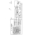
- FIG. 1 is a configuration diagram of the wire bonding apparatus 10.
- the wire bonding apparatus 10 is an apparatus that uses a capillary 28 as a wire bonding tool, an aluminum wire as a wire 30, and connects two bonding objects with the wire 30 by a wedge bonding method.
- a semiconductor chip 6 and a circuit board 8 are shown as bonding objects.
- the wedge bonding method refers to a bonding method that uses ultrasonic waves and pressure without forming a FAB at the wire tip.
- the wire bonding apparatus 10 includes a bonding stage 14 held on a gantry 12, an XY stage 16, and a computer 60.
- the bonding stage 14 is a bonding object holding base on which the semiconductor chip 6 and the circuit board 8 which are two bonding objects are mounted.
- the bonding stage 14 is movable with respect to the gantry 12 when the circuit board 8 or the like is mounted or ejected, but is fixed to the gantry 12 during the bonding process.
- a metal moving table can be used as the bonding stage 14.
- the bonding stage 14 is connected to a reference potential such as the ground potential of the wire bonding apparatus 10.
- the bonding stage 14 is connected to a ground side terminal of a non-sticking determination circuit 36 described later.
- the semiconductor chip 6 is an electronic circuit in which transistors and the like are integrated on a silicon substrate. An input terminal and an output terminal as an electronic circuit are drawn out as a plurality of pads (not shown) on the upper surface of the semiconductor chip 6. Yes.
- the lower surface of the semiconductor chip 6 is the back surface of the silicon substrate and serves as a ground electrode for an electronic circuit.
- the circuit board 8 is obtained by patterning desired wiring on an epoxy resin substrate, and is disposed around a chip pad (not shown) for electrically and mechanically connecting and fixing the lower surface of the semiconductor chip 6. It has a plurality of leads (not shown), and an input terminal and an output terminal as a circuit board drawn from the chip pad or the plurality of leads. Wire bonding is performed by connecting the pads of the semiconductor chip 6 and the leads of the circuit board 8 with wires 30.
- the wind clamper 50 provided on the bonding stage 14 is a flat plate member having an opening at the center, and is a member that holds the circuit board 8.
- the wind clamper 50 is positioned so that the lead of the circuit board 8 on which wire bonding is performed and the semiconductor chip 6 are arranged in the opening at the center, and holds the circuit board 8 at the peripheral edge of the opening.
- the circuit board 8 is fixed to the bonding stage 14.
- the XY stage 16 is a moving table that mounts the bonding head 18 and moves the bonding head 18 to a desired position in the XY plane with respect to the gantry 12 and the bonding stage 14.
- the XY plane is a plane parallel to the upper surface of the gantry 12.
- the Y direction is a direction parallel to the longitudinal direction of the ultrasonic transducer 24 attached to a bonding arm (not shown) described later.
- FIG. 1 shows the X direction, the Y direction, and the Z direction, which is a direction perpendicular to the XY plane.
- the bonding head 18 is mounted on the XY stage 16 and is a moving mechanism that incorporates a Z motor 20 and moves the capillary 28 in the Z direction via the Z drive arm 22 and the ultrasonic transducer 24 by rotation control. is there.
- a linear motor can be used as the Z motor 20.
- the Z drive arm 22 is a member to which an ultrasonic transducer 24 and a wire clamper 32 are attached, and is rotatable around a rotation center provided in the bonding head 18 by rotation control of the Z motor 20.
- the center of rotation provided in the bonding head 18 is not necessarily the output shaft of the Z motor 20, and the entire center of gravity including the Z drive arm 22, the ultrasonic transducer 24, and the wire clamper 32 is taken into consideration, and the rotational load is reduced. Set to position.
- the ultrasonic transducer 24 is an elongated rod member having a root portion attached to the Z drive arm 22 and a capillary 28 through which the wire 30 is inserted at the tip portion.
- An ultrasonic transducer 26 is attached to the ultrasonic transducer 24 and transmits ultrasonic energy generated by driving the ultrasonic transducer 26 to the capillary 28. Therefore, the ultrasonic transducer 24 is formed in a horn shape that tapers toward the distal end side so that the ultrasonic energy from the ultrasonic transducer 26 can be efficiently transmitted to the capillary 28.
- a piezoelectric element is used as the ultrasonic transducer 26.
- the capillary 28 is a bonding tool having a conical body with a flat tip surface and a through-hole through which the wire 30 can be inserted along the longitudinal direction.
- a ceramic capillary used for ball bonding can be used as it is.
- Capillaries used for ball bonding are provided with a corner shape called an appropriate chamfer on the tip surface side of the through hole so that the FAB can be easily held.
- ball bonding is performed.
- a flat surface called a face is provided on the lower surface of the through-hole of the capillary on the tip surface side. This face serves as a pressing surface when wedge bonding is performed in the wire bonding apparatus 10.
- the tool for wedge bonding has a wire guide provided obliquely with respect to the longitudinal direction at the tip, and a pressing surface for pressing the side surface of the wire, it is not rotationally symmetric around the longitudinal axis of the tool, The wire protrudes laterally with directionality along the direction of the wire guide.
- the direction of the wire guide may not match the wire connection direction.
- the semiconductor chip 6 is mounted on the center portion of the circuit board 8, a plurality of pads are arranged so as to make a round along the peripheral portion of the semiconductor chip 6, and the circuit board 8 also extends along the outside of the semiconductor chip 6.
- the connection direction of the wire connecting the lead and the pad differs depending on each of the plurality of wire bondings. In order to align the direction of the wire guide with the connecting direction of the wire, it is necessary to rotate the wedge bonding tool around the longitudinal axis or rotate the circuit board 8.
- the connection direction of the wire connecting the pad and the lead may be different for each wire bonding. It is only necessary to perform a shaping process for slightly changing the direction of the wire 30 protruding from the tip of the capillary 28. For this reason, the capillary 28 is used for wedge bonding.
- the wire 30 inserted through the capillary 28 is a thin aluminum wire.
- the wire 30 is wound around a wire spool 33 provided at the tip of a wire holder extending from the bonding head 18, and is inserted from the wire spool 33 through the wire clamper 32 into a through hole in the center of the capillary 28, thereby leading the tip of the capillary 28. Stick out from.
- a material of the wire 30 in addition to a pure aluminum thin wire, a thin wire appropriately mixed with silicon, magnesium or the like can be used.
- the diameter of the wire 30 can be selected according to the bonding object. An example of the diameter of the wire 30 is 30 ⁇ m.
- the wire clamper 32 is attached to the Z drive arm 22 and is a pair of sandwich plates arranged on both sides of the wire 30.
- the wire clamper 32 is configured to freely move the wire 30 by opening between the opposite sandwich plates and to close between the opposite sandwich plates.
- a wire pinching device for stopping the movement of the wire 30. Since the wire clamper 32 is attached to the Z drive arm 22, even if the capillary 28 moves in the XYZ directions, the wire 30 can be properly sandwiched.
- the wire clamper 32 is opened and closed by the operation of a clamper opening / closing unit 34 using a piezoelectric element.
- the non-sticking determination circuit 36 is a circuit that determines whether or not the connection between the bonding object and the wire 30 is appropriate at each stage of wire bonding.
- the non-sticking determination circuit 36 applies a predetermined electrical signal between the bonding object and the wire 30 and determines whether or not the connection between the bonding object and the wire 30 is appropriate based on the response.
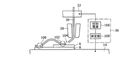
- FIG. 2 is a configuration diagram of the non-stick determination circuit 36.
- the wire bonding is appropriately performed at the first bond point 100, and then, after passing through the loop forming process, the process proceeds to the second wire bonding process, and the second wire bonding process is also the second.
- FIG. 3 is a diagram showing that wire bonding has been properly performed at the bond point 102, and then the wire cutting process has been performed appropriately, and the wire 30 is in the cut state 104 at the second bond point 102. It is. Thus, the time when each processing step of wire bonding is normally performed is shown.
- the non-sticking determination circuit 36 includes an applied power source 106 and a measurement unit 108, one terminal is connected to the bonding stage 14, and the other terminal is connected to the wire clamper 32 or the wire spool 33.
- an impedance measurement circuit (not shown) inside the measurement unit 108 using the applied power source 106 as an AC voltage power source, the capacitance component between the wire 30 and the bonding stage 14 can be obtained.
- a DC pulse power supply may be used in place of the applied power supply 106 instead of the AC voltage power supply.
- the applied power source 106 is an AC voltage power source.
- the capacitance component value between the wire clamper 32 and the bonding stage 14 is the capacitance value of the element of the wire bonding apparatus 10.
- the total value of the capacitance value and the device capacitance value that is the capacitance value of the circuit board 8 or the semiconductor chip 6 is obtained.
- the wire 30 and the circuit board 8 or the semiconductor chip 6 are in an electrically open state, so that the value of the capacitance component between the wire clamper 32 and the bonding stage 14 is reached. Is only the device capacity value.
- the non-sticking determination circuit 36 can determine whether the connection between the wire 30 and the circuit board 8 or the semiconductor chip 6 that is the bonding target is in a connected state or an open state.
- the non-sticking determination circuit 36 makes a determination as follows in each process step. After the first wire bonding process at the first bond point 100, the capacitance value between the wire clamper 32 or the wire spool 33 and the bonding stage 14 becomes the total value of the device capacitance value and the device capacitance value, so that the wire 30 And the circuit board 8 are determined to be in a connected state. Even when the capillary 28 descends toward the second bond point 102 and contacts the second bond point 102, the capacitance value between the wire clamper 32 and the bonding stage 14 is the sum of the device capacitance value and the device capacitance value. Thus, it is determined that the wire 30 and the circuit board 8 are in a connected state.
- the distance between the wire clamper 32 and the bonding stage 14 becomes the total value of the device capacitance value and the device capacitance value. Is determined to be connected.
- the capacitance value between the wire clamper 32 and the bonding stage 14 becomes the value of the device capacitance value, so that it is determined that the wire 30 and the semiconductor chip 6 are in a disconnected state.
- the computer 60 controls the operation of each element of the wire bonding apparatus 10 as a whole.
- the computer 60 includes a control unit 80 that is a CPU, various interface circuits, and a memory 82. These are connected to each other by an internal bus.
- the various interface circuits are drive circuits or buffer circuits provided between the control unit 80, which is a CPU, and each element of the wire bonding apparatus 10.
- the interface circuit is simply indicated as I / F.
- Various interface circuits include an XY stage I / F 62 connected to the XY stage 16, a Z motor I / F 64 connected to the Z motor 20, an ultrasonic vibrator I / F 66 connected to the ultrasonic vibrator 26, and a clamper opening / closing.
- a clamper opening / closing I / F 68 connected to the unit 34, and a non-sticking determination circuit I / F 70 connected to the non-sticking determination circuit 36.
- the memory 82 is a storage device that stores various programs and various control data.
- the various programs are a first bonding program 84 related to the first wire bonding process, a loop forming program 86 related to the loop forming process, a second bonding program 88 related to the second wire bonding process, and a non-continuous continuous monitoring program related to the continuous monitoring process by the non-sticking determination circuit 36.
- 90 a cutting determination processing program 92 related to the determination processing of the midway cutting of the wire 30, an abnormal output processing program 94 related to an abnormal signal output indicating that the midway cutting of the wire 30 has occurred, and a control program 96 related to other control processing.
- the control data 98 is data necessary for executing various programs and control programs.
- FIG. 3 is a time chart showing the operation of each element in the wire bonding process.
- FIG. 4 is a flowchart showing the procedure of the wire bonding method.
- FIG. 5 is a time chart showing each signal related to non-contact monitoring between the first bond point and the second bond point in association with the movement of the capillary 28.
- 6 to 9 are diagrams showing the state of the wire between the first bond point and the second bond point, respectively.
- FIG. 3 is a time chart showing the operation state of each element from the first wire bonding process at the first bond point 100 to the second wire bonding process and the wire cutting at the second bond point 102 through the loop formation process. is there.
- the horizontal axis in FIG. 3 is time.
- the vertical axis in FIG. 3 indicates the height of the capillary 28, whether the Z motor 20 is operating or stopped, whether the XY stage 16 is operating or stopped, and the ultrasonic transducer in order from the upper side to the lower side.
- Whether 26 is an operation state or a stop state, the magnitude of the pressing force pressing the capillary 28 downward, and whether the wire clamper 32 is closed or open are shown.
- the height state of the capillary 28 changes when the Z motor 20 is operating, and does not change when the Z motor 20 is stopped.
- the Z motor 20 is driven via the Z motor I / F 64 when the control unit 80 executes various programs. If there is, it is done by stopping the operation.
- the capillary 28 changes its position in the XY plane by moving in the XY plane.
- the movement of the capillary 28 in the XY plane is controlled by moving and driving the XY stage 16 via the XY stage I / F 62 when there is a movement command for the XY stage 16 when the control unit 80 executes various programs. When there is a command, this is done by stopping the movement drive.
- ultrasonic energy is supplied from the ultrasonic transducer 26 to the capillary 28.
- the ultrasonic energy supply from the ultrasonic transducer 26 is controlled by the ultrasonic wave via the ultrasonic transducer I / F 66 when an operation command for the ultrasonic transducer 26 is issued when the control unit 80 executes various programs. This is done by operating the vibrator 26 and stopping the operation when there is a stop command.
- a predetermined pressing force is applied to the capillary 28 via the ultrasonic transducer 24.
- the magnitude of the pressing force can be controlled as part of the drive control of the Z motor 20. That is, when the controller 80 executes various programs, if there is a pressing force change command, the pressing force is changed by driving control of the Z motor 20 via the Z motor I / F 64.
- the wire clamper 32 is opened when the wire 30 is extended from the capillary 28, and the wire clamper 32 is closed when the extension of the wire 30 is stopped and clamped.
- the wire clamper 32 opening / closing control causes the clamper opening / closing unit 34 to open the wire clamper 32 via the clamper opening / closing I / F 68 if there is an open operation command for the wire clamper 32.
- a closing operation command it is performed by causing the clamper opening / closing unit 34 to close the wire clamper 32.
- the period from the time t 0 to the time t 4 is the period of the first wire bonding process, and the controller 80 executes the first bonding program 84 during this period.
- the XY stage 16 is driven to move and the capillary 28 is moved immediately above the first bond point.
- the Z motor 20 is driven from time t 0 to time t 3 , whereby the capillary 28 continues to descend. Descent, until time to move t 1 is fast falling from time t 0 to just above the capillary 28 is in the first bonding point 100, during the time t 3 when in contact from the time t 1 to the lead capillary 28 of the circuit board 8 Slow. This low speed descent is called a first search (1st search).
- the XY stage 16 and the Z motor 20 are both in a stopped state, and during this period, the ultrasonic vibrator 26 is operated to apply ultrasonic energy to the capillary 28.
- the pressing force changes stepwise from the time t 1 to the time before and after the start of the operation of the ultrasonic transducer 26.
- the wire 30 protruding from the tip of the capillary 28 is sandwiched between the tip of the capillary 28 and the lead of the circuit board 8 at the first bond point 100. Bonding between the wire 30 and the lead is performed by ultrasonic energy and pressing force.
- the bonding stage 14 is heated and maintained at an appropriate processing temperature.
- the period from the time t 4 to the time t 10 is the period of the loop forming process. At this time, the pressing force is restored. In this period, the control unit 80 executes the loop formation program 86. As shown in FIG. 3, only the Z motor 20 is driven from time t 4 to time t 5 , thereby raising the capillary 28 slightly. Between the time t 5 the time t 6, only the XY stage 16 is driven movement. This movement drive is performed as a reverse movement in which the capillary 28 is once returned from the first bond point 100 to the opposite side of the second bond point 102 in the XY plane.
- the wire clamper 32 is opened, and the wire 30 can be extended from the tip of the capillary 28. Then, during the time t 10 from the time t 9, XY stage 16 is driven movement, Z motor 20 is driven. As a result, the capillary 28 is lowered while the wire 30 is extended toward the second bond point 102, and the loop is lowered downward.
- the capillary 28 comes immediately above the second bond point 102.
- the period from the time t 10 to the time t 13 is the period of the second wire bonding process at the second bond point 102.
- the control unit 80 executes the second bonding program 88.
- Lowering the capillary 28 is a fast falling from time t 9 the capillary 28 to the time t 10 to move immediately above the second bonding point 102, the time t 12 to the capillary 28 from the time t 10 is in contact with the pads of the semiconductor chip 6 During this period, the speed is low. This low speed drop is called a second search (2nd search).
- the time t 13 is a also stopped XY stage 16 also Z motor 20, gives the ultrasonic transducer 26 is activated by ultrasonic energy during this period the capillary 28.
- the pressing force changes stepwise from the time t 10 to the time before and after the start of the operation of the ultrasonic transducer 26.
- the wire 30 protruding from the tip of the capillary 28 is sandwiched between the tip of the capillary 28 and the pad of the semiconductor chip 6 at the second bond point 102, Bonding between the wire 30 and the lead is performed by ultrasonic energy and pressing force.
- the bonding stage 14 is heated and maintained at an appropriate processing temperature.
- the wire cutting process is distinguished from the second wire bonding process, and the controller 80 can execute a dedicated wire cutting process program. Alternatively, this period may be included in the second wire bonding process, and the wire cutting process program may be included in the second bonding program 88.
- the pressing force is restored. As shown in FIG. 3, it is driven only while Z motor 20 for time t 13 from the time t 14, whereby the capillary 28 is slightly increased. Between the time t 14 the time t 15 is wire clamper 32 is closed, XY stage 16 is driven movement, Z motor 20 is driven. This movement drive is performed on the assumption that the capillary 28 moves in the XY plane while rising. As a result, the wire 30 is cut at the second bond point 102.
- the second wire bonding process and the wire cutting at the second bond point 102 are performed through the loop formation process from the first wire bonding process at the first bond point 100.
- FIG. 4 is a flowchart showing the procedure from the first wire bonding process to the second wire bonding process in the procedure of the wire bonding method.
- Each procedure is a process of each program stored in the memory 82 of the computer 60. Corresponds to the procedure.
- a power supply or the like is turned on to the wire bonding apparatus 10
- each component of the wire bonding apparatus 10 including the computer 60 is initialized.
- the bonding stage 14 is pulled out once, and the circuit board 8 on which the semiconductor chip 6 as a bonding target is mounted is positioned and set on the bonding stage 14 and is pressed and fixed by the wind clamper 50.
- the bonding stage 14 is returned to the initial position again.
- the bonding stage 14 is heated to a predetermined temperature determined by the bonding conditions.
- This bonding object setting step is automatically performed using an automatic transfer device for the circuit board 8.
- the first bonding program 84 is executed by the control unit 80, and the first wire bonding process is performed at the first bond point 100 (S10).
- the first bond point 100 is set on one lead of the circuit board 8.
- the first bond point 100 is set using a positioning camera or the like not shown in FIG. Since the operation of each element in the first wire bonding process has been described with reference to FIG. 3, detailed description thereof will be omitted.
- the wire 30 is sandwiched and pressed between the tip of the capillary 28 and the lead of the circuit board 8, and the capillary 28 is controlled by the ultrasonic vibration energy of the ultrasonic vibrator 26 and the drive control of the Z motor 20.
- the wire 30 and the lead are bonded to each other by the pressing force and, if necessary, the heating temperature from the bonding stage 14. In this way, the first wire bonding process at the first bond point 100 is performed.
- a loop forming process is performed (S12). This processing procedure is performed by the control unit 80 executing the loop formation program 86. That is, after the first wire bonding process is completed, the capillary 28 is lifted upward with the wire clamper 32 open, and then moved directly above the second bond point 102. The second bond point 102 is set on one pad of the semiconductor chip 6. During the movement of the capillary 28, the wire 30 is drawn out from the wire spool 33 and extended from the tip of the capillary 28 by a necessary wire length. Since the operation of each element in the loop forming process has been described with reference to FIG. 3, a detailed description thereof will be omitted.
- continuous non-delivery monitoring is performed (S14). This processing procedure is performed by the control unit 80 executing the non-delivery continuous monitoring program 90.
- the non-stick continuous monitoring is performed by continuously operating the non-stick determination circuit 36 via the non-stick determination circuit I / F 70 according to a command from the control section 80, and the control section 80 continuously receives the result.
- the continuous operation of the non-sticking determination circuit 36 continuously operates the AC voltage power source, which is the applied power source 106 described with reference to FIG. 2, during a predetermined continuous monitoring period.
- an AC voltage signal is continuously applied between the wire 30 held by the capillary 28 and the bonding stage 14.
- the measurement unit 108 described with reference to FIG. 2 acquires the capacitance value between the wire 30 held in the capillary 28 and the bonding stage 14 and sequentially calculates the value via the non-attachment determination circuit I / F 70.
- the data is transmitted to the control unit 80.
- Whether or not the wire is cut halfway is determined by continuous non-bonding monitoring (S16). This processing procedure is performed by the control unit 80 executing the cutting determination processing program 92.
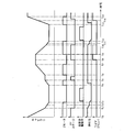
- FIG. 5 shows the temporal change of each signal in the non-attachment continuous monitoring in association with the operating state of the capillary 28.
- the horizontal axis in FIG. 5 is time.
- the vertical axis represents the operating state of the capillary 28, the non-sticking monitoring output which is the output of the measuring unit 108 of the non-sticking judgment circuit 36, the differential output obtained by differentiating the non-sticking monitoring output in order from the upper side to the lower side of the paper surface. This is the timing of non-delivery monitoring.
- the time t 4 , t 7 , t 9 , t 12 on the horizontal axis is the same as that described in FIG. That is, the time t 4 is the timing at which the joining process at the first bond point 100 is completed and the loop forming process is started, the period during which the loop is formed at the highest position from time t 7 to time t 9 , and t 12 is This is the timing at which the capillary 28 descends and contacts the second bond point 102.
- Times T 1 , T 2 , and T 3 are non-delivery monitoring timings in the prior art, as shown at the bottom of FIG.
- just prior to time t 4 immediately after the time t 7, it is set to the timing after the t 12. This is merely an example, and non-delivery monitoring may be performed at other appropriate sampling timings.
- the non-sticky determination circuit 36 continues to operate during a preset continuous monitoring period instead of the conventional sampling timing.
- the continuous monitoring period is set to a period suitable for monitoring whether or not the wire 30 is cut between the first bond point and the second bond point after the first bonding process.
- the entire period from the first bond point to the second bond point is set as the continuous monitoring period.
- the continuous monitoring period may be between T 1 and T 3 used in the prior art.
- T 1 and T 3 of the non-contact monitoring sampling timing of the prior art may be left as they are, and the continuous monitoring period may be from time t 7 when the capillary 28 is at the highest position to time t 12 when the capillary 28 is at the lowest position.
- the non-sticking monitoring output is an output of the measurement unit 108 of the non-sticking determination circuit 36, and shows a temporal change in the capacitance value.
- Figure 5 for example, to maintain a substantially capacitance value of the constant value from time C 0 of the capillary 28 is rising to the time C 1, suddenly capacitance value decreases with time C 1.
- the capacitance value detected by the measurement unit 108 changes from “total value of device capacitance value and device capacitance value” to “device capacitance value”, and therefore it is determined that the wire 30 has been cut at time C 1. Can do.
- the reduced capacity value is maintained from time C 1 to time C 2 , but the capacity value suddenly recovers to the original high value at time C 2 .
- the wire 30 is cut in the middle of the loop. Can be judged. Further, when the capacitance value recovers until reaching the second bond point thereafter, it can be determined that the cut wire 30 hangs down and contacts the circuit board 8 or the semiconductor chip 6 that is the bonding target.
- the capacitance value does not change at the same value at any of the times T1, T2, and T3.
- the presence or absence of the midway cut of the wire 30 is determined by the change in the capacitance value.
- the presence or absence of a change in the capacitance value can be detected by comparing the threshold capacitance value using the threshold capacitance value. Instead of this, it is possible to determine whether or not the wire 30 is cut halfway based on a differential value obtained by differentiating an electric signal indicating a capacitance value with respect to time.
- the differential output in FIG. 5 is obtained by differentiating the non-delivery monitoring output with respect to time. When the capacitance value rapidly decreases, a negative pulse is output, and when the capacitance value increases and recovers rapidly, a positive pulse is output. Based on the presence or absence of this pulse output, it can be determined whether or not the wire 30 is cut halfway.
- 6 to 9 are diagrams showing the state of the wire 30 at time t 4 , time C 0 , time C 1 , and time C 2 .
- the capacitance value detected by the measurement unit 108 is “the total value of the device capacitance value and the device capacitance value”.
- the capillary 28 has moved X1 from the first bond point 100 in the XY plane, and the height in the Z direction has risen to Z1 with respect to the upper surface of the circuit board 8.
- the wire 30 is extended from the capillary 28 in a state where the wire 30 is bonded to the circuit board 8 at the first bond point 100.
- the capacitance value detected by the measurement unit 108 is “the total value of the device capacitance value and the device capacitance value”.
- the time C 1 shown in FIG. 8 is when the height of the capillary 28 in the Z direction reaches the maximum value Z2, the wire clamper 32 is closed, and the XY stage 16 moves from the first bond point 100 by the distance X2 in the XY plane. (See FIG. 3).
- the wire 30 is in the cut state 104 between the first bond point 100 and the tip of the capillary 28.
- the wire 30 extends from the capillary 28 toward the first bond point 100, and the cut portion is a tip portion 105.
- the above-described state of the time C 1 at which cutting occurs is an example, and cutting may occur in other states as long as it is on the way from the first bond point 100 to the second bond point 102.
- the capacitance value detected by the measurement unit 108 becomes “apparatus capacity value”, and the capacitance value rapidly decreases from “total value of apparatus capacity value and device capacity value”. According to the non-attachment continuous monitoring, it can be determined that the wire 30 has been cut in the middle of the loop by detecting a sudden drop in the capacitance value.
- the time C 2 shown in FIG. 9 is a distance X3 from the first bond point 100 while the capillary 28 descends in the Z direction to the height of Z3 and moves in the XY plane, and the tip of the capillary 28 moves to the second bond point. It is when it came just above 102.
- Z 3 is a value smaller than Z 2 in FIG. 8
- X 3 is a value larger than X 2 in FIG.
- the tip portion 105 of the wire 30 extending from the capillary 28 comes into contact with the circuit board 8 due to the lowering of the capillary 28.
- the capacitance value detected by the measurement unit 108 rapidly increases to “the total value of the device capacitance value and the device capacitance value” and recovers.
- the second wire bonding process is performed at the second bond point 102 (S18). ).
- This processing procedure is performed by the control unit 80 executing the second bonding program 88.
- the second bond point 102 is set on one pad of the semiconductor chip 6.
- the second bond point 102 is set using a positioning camera or the like not shown in FIG. Since the operation of each element in the second wire bonding process has been described with reference to FIG. 3, detailed description thereof will be omitted.
- the first bond point 100 can be used.
- the presence or absence of wire cutting between the second bond points 102 can be accurately determined.
- the predetermined continuous monitoring period is a period in which the wire is extended from the first bond point to the second bond point after the first bonding process, but the second bonding process is performed before the first bonding process. It is also possible to set a continuous monitoring period over the entire period until later.
- the non-sticking monitoring unit continuously applies a predetermined electrical signal between the wire 30 held in the capillary 28 and the bonding stage 14. And the presence or absence of the change of the connection state of the wire 30 is monitored and judged with respect to the continuous response using an appropriate judgment threshold value.
- Wire non-bonding at the first bond point is F1
- wire halfway cutting during the loop formation period is F2
- wire non-bonding at the second bond point is F3
- the wire before the wire cutting process after the second bonding process Assuming that the middle cut is F4, an appropriate determination threshold is used for each of F1 to F4. In this way, F1 to F4 can be distinguished and monitored.
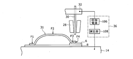
- FIG. 10 is a view corresponding to FIG. 6 to FIG. 9, and further expands the state shown in these, and the bonding of the wire 30 is performed for the entire period from before the first bonding process to after the second bonding.
- FIG. Here, the first bonding process performed on the first bond point of the circuit board 8, the loop forming process after the first bonding process, and the second bonding performed on the second bond point of the semiconductor chip 6 after the loop forming process. After the process and the second bonding process, the wire 31 that has been performed without any problem up to the cutting process for cutting the wire 30 is shown.
- F1 which is a wire non-bonding at the first bond point
- F2 which is a wire cut in the loop formation period
- F3 which is a wire non-bonding at the second bond point
- F4 which is the midway cut of the wire before
- the non-sticking determination circuit 36 shown in FIG. 10 has the same contents as those described with reference to FIG. 2 and includes an applied power source 106 that outputs a predetermined electric signal and a measurement unit 108 that measures a response to the predetermined electric signal.
- an AC voltage signal or a DC voltage signal is used as the predetermined electrical signal.
- This proper use can be determined by whether the semiconductor chip 6 and the circuit board 8 can be regarded as being connected to the bonding stage 14 only by an electrical resistance component.
- a DC voltage signal can be used as a predetermined electrical signal.
- an AC voltage signal is used as a predetermined electrical signal.
- the measuring unit 108 measures a change in the capacitance value between the wire 30 via the wire clamper 32 and the bonding stage 14.
- the capacitance value can be converted into a voltage value using an appropriate conversion circuit, and the change in the capacitance value can be measured by measuring the change in the converted voltage value.
- the measurement unit 108 measures a change in the presence or absence of an electrical short circuit between the wire 30 via the wire clamper 32 and the bonding stage 14.
- FIG. 11 is a diagram showing that F1 to F4 can be distinguished when an AC voltage signal is used as a predetermined electrical signal and a capacitance value between the wire 30 and the bonding stage 14 is measured as a continuous response. is there.
- FIG. 11 includes six time charts (a) to (f). In all of these, the horizontal axis is time.
- the vertical axis of (a) is the height position of the capillary, and the vertical axis of (b) to (f) is the capacitance value between the wire 30 and the bonding stage 14.
- FIG. 11A corresponds to the uppermost drawing of FIG. Times t 3 , t 4 , t 12 , t 13 , and t 14 on the horizontal axis are the same as those described in FIG. That is, the period from time t 3 to t 4 is the period of the first bonding process, the period from t 12 to t 13 is the period of the second bonding process, and t 14 is the period of the wire clamper 32 after the second bonding process. This is the timing at which the wire 30 is cut by the operation.
- FIG. 11B is a time chart showing the change over time of the capacitance value measured for a non-defective product in which all the processes were performed without any problem for the entire period from before the first bonding process to after the second bonding. is there.
- the capacitance value is the device capacitance value between the wire 30 and the bonding stage 14 via the wire bonding apparatus 10.
- the capacitance value of the circuit board 8 is added and measured.
- the capacitance value included in the circuit board 8 shown as C L. Therefore, the measured value of the capacitance value during the period from time t 3 to time t 12 is (C M + C L ).
- Wire 30 is cut by a cutting process at time t 14, when a state shown in FIG. 10, the wire 30 is not in contact at a distance from the semiconductor chip 6 on the circuit board 8, the measurement value of the capacitance value, again the device capacitance C M.
- FIG. 11C is a time chart showing the change over time of the capacitance value when the non-bonding F1 occurs at the first bond point.
- Non-delivery F1 occurs between times a period of the first bonding process t 3 and time t 4.
- the wire 30 is not firmly connected to the circuit board 8, so that the capacitance value is smaller than the capacitance value (C M + C L ) at the time t 3 when it is a good product.
- the capacitance value stably measured before t 3 can be used as a reference.
- a value obtained by adding a predetermined measurement margin to the capacitance value C M before t 3 is set as a first reference value J1
- the first reference value J1 is a determination threshold value for discriminating between non-defective products and F1.
- the was J1 C M.
- the measured capacitance value exceeds J1, it is judged as non-defective, and when it is less than J1, it is judged as F1.
- the measured capacitance value is (C M + C L ), and in the example of F1, the measured capacitance value remains C M.
- the process at the first bond point is normal, and the measured capacitance value becomes (C M + C L ) at time t 3.
- the wire 30 is cut halfway F2 It is a time chart which shows the time change of the capacitance value when this occurs.
- Half-way disconnection F2 occurs between times t 4 and time t 12.
- the wire 30 is separated from the circuit board 8, so that the measured capacitance value is smaller than the capacitance value (C M + C L ) at time t 4 when the product is a non-defective product.
- the capacitance value (C M + C L ) at t 4 is used as a reference, a value obtained by adding a predetermined measurement margin to (C M + C L ) is set as a second reference value J2, and the second reference value J2 is set as the second reference value J2. It is used as a judgment threshold for distinguishing between non-defective products and F2.
- J2 (C M + C L ).
- FIG. 11 (e) is a time chart showing the change over time of the capacitance value when the loop formation processing is normal but the non-attachment F3 occurs at the second bond point.
- Non-delivery F3 occurs between time t 12 and time t 13.
- the wire 30 is not firmly connected to the semiconductor chip 6, so that the capacitance value is smaller than the capacitance value (C M + C L + C P ) at time t 12 when the product is a good product. .
- the capacitance value (C M + C L ) at t 4 is used as a reference, and a value obtained by adding a predetermined measurement margin to (C M + C L ) is set as a third reference value J3. It is used as a judgment threshold for distinguishing between non-defective products and F3.
- An example of a non-defective product has a measured capacitance value (C M + C L + C P ), and an example of F3 has a measured capacitance value (C M + C L ).
- FIG. 11 (f) shows that the process at the second bond point is normal, and the measured capacitance value becomes (C M + C L + C P ) at time t 12 , but before the subsequent wire cutting process, 6 is a time chart showing a change over time of a capacitance value when an intermediate cut F4 of the wire 30 occurs.
- Half-way disconnection F4 occurs between time t 13 and time t 14.
- the wire 30 is separated from the semiconductor chip 6, so that the measured capacitance value is smaller than the capacitance value (C M + C L + C P ) at the time t 13 when the product is good.
- the capacitance value (C M + C L + C P ) at t 13 is used as a reference, and a value obtained by subtracting a predetermined measurement margin from (C M + C L + C P ) is set as a fourth reference value J4.
- the reference value J4 is used as a judgment threshold value for distinguishing between non-defective products and F4.
- J4 (C M + C L + C P ).
- FIG. 12 is a diagram showing that F1 to F4 can be distinguished when a DC voltage signal is used as a predetermined electrical signal and a voltage value between the wire 30 and the bonding stage 14 is measured as a continuous response. is there.
- FIG. 12 is a diagram corresponding to FIG. 11 and includes six time charts (a) to (f). As in FIG. 11, in all of these, the horizontal axis is time. The vertical axis in (a) is the height position of the capillary, and the vertical axis in (b) to (f) is the voltage value between the wire 30 and the bonding stage 14.
- FIG. 12A corresponds to the uppermost drawing of FIG. 3 as in FIG. 11A. Since the time t 3 , t 4 , t 12 , t 13 , and t 14 on the horizontal axis are the same as those in FIG. 11 and the same as the contents described in FIG. 3, detailed description thereof is omitted.
- FIG. 12B is a time chart showing a time change of a measured voltage value for a non-defective product in which all the processes are performed without any problem for the entire period from before the first bonding process to after the second bonding. is there.
- FIG. 12C is a time chart showing a time change of the voltage value when the non-bonding F1 occurs at the first bond point.
- Non-delivery F1 occurs between times a period of the first bonding process t 3 and time t 4.
- the wire 30 is not firmly connected to the circuit board 8, so that there is no electrical short circuit between the wire 30 and the bonding stage 14. Therefore, the voltage value remains at the predetermined voltage value V 0 that is the voltage value at time t 3 when the product is non-defective.
- a voltage value stably measured before t 3 can be used as a reference.
- the wire 30 is cut halfway F2 It is a time chart which shows the time change of the voltage value when this occurs.
- Half-way disconnection F2 occurs between times t 4 and time t 12.
- the cut F2 occurs in the middle, the wire 30 is separated from the circuit board 8, so that there is no electrical short circuit between the wire 30 and the bonding stage 14, and the measured voltage value is the time t when the product is good.
- J2 0 (V).
- FIG. 12E is a time chart showing the time change of the voltage value when the loop formation processing is normal but the non-bonding F3 occurs at the second bond point.
- Non-delivery F3 occurs between time t 12 and time t 13.
- the wire 30 is not firmly connected to the semiconductor chip 6, so that there is no electrical short circuit between the wire 30 and the bonding stage 14. Therefore, the voltage value becomes the predetermined voltage value V 0 .
- the wire bonding at the first bond point and the second bond point has been described as a wedge bonding method using a capillary, but this may be performed by a ball bonding method.
- the present invention can be used in an apparatus and a method for performing wire bonding using a capillary.
Landscapes
- Engineering & Computer Science (AREA)
- Mechanical Engineering (AREA)
- Wire Bonding (AREA)
Abstract
Description
Claims (14)
- ワイヤボンディングの第1ボンド点において、ボンディング対象物とワイヤとの間を接合する第1ボンディング処理部と、
前記第1ボンディング処理の後、所定の連続監視期間の間、キャピラリに保持されている前記ワイヤと前記ボンディング対象物との間に所定の電気信号を連続的に印加し、その連続的応答に基づいて前記ワイヤと前記ボンディング対象物との間の接続が変化するか否かを監視し判断する不着監視部と、
を備える、ワイヤボンディング装置。 - 請求項1に記載のワイヤボンディング装置において、
前記所定の連続的監視期間は、
前記第1ボンディング処理の後、前記第1ボンド点から前記ワイヤボンディングの第2ボンド点まで前記ワイヤを延出する期間である、ワイヤボンディング装置。 - 請求項2に記載のワイヤボンディング装置において、
前記不着監視部は、
前記キャピラリに保持されている前記ワイヤと前記ボンディング対象物との間に所定の電気信号を印加して前記キャピラリに保持されている前記ワイヤと前記ボンディング対象物との間の容量値を取得し、前記第1ボンディング処理の後で前記容量値が低下したときに前記ボンディング対象物から前記ワイヤが切断されたと判断し、その後前記第2ボンド点に至るまでに前記容量値が回復するときは、前記切断された前記ワイヤが前記ボンディング対象物に垂れて接触したと判断する、ワイヤボンディング装置。 - 請求項3に記載のワイヤボンディング装置において、
前記所定の電気信号とは、交流電気信号、直流パルス信号のいずれかである、ワイヤボンディング装置。 - 請求項3又は4に記載のワイヤボンディング装置において、
前記不着監視部は、
前記取得した前記容量値を時間について微分した微分値に基づいて、前記容量値についての低下と回復を判断する、ワイヤボンディング装置。 - 請求項1から5のいずれか1に記載のワイヤボンディング装置において、
前記第1ボンド点および前記第2ボンド点における前記ワイヤボンディングは、ウェッジボンディング方式で行われる、ワイヤボンディング装置。 - ワイヤボンディングの第1ボンド点において、ボンディング対象物とワイヤとの間を接合する第1ボンディング処理工程と、
前記第1ボンディング処理の後、前記第1ボンド点から前記ワイヤボンディングの第2ボンド点まで前記ワイヤを延出する期間の間、キャピラリに保持されている前記ワイヤとボンディング対象物との間に所定の電気信号を連続的に印加して前記キャピラリに保持されている前記ワイヤと前記ボンディング対象物との間の容量値の変化を取得する連続監視工程と、
前記第1ボンディング処理の後で前記容量値が低下したときに前記ワイヤが途中切断されたと判断し、その後前記第2ボンド点に至るまでに前記容量値が回復するときは、前記途中切断された前記ワイヤが前記ボンディング対象物に垂れて接触したと判断する途中切断判断工程と、
を有する、ワイヤボンディング方法。 - 請求項7に記載のワイヤボンディング方法において、
前記所定の電気信号とは、交流電気信号、直流パルス信号のいずれかである、ワイヤボンディング方法。 - ワイヤボンディングの第1ボンド点において、第1ボンディング対象物とワイヤとの間を接合する第1ボンディング処理部と、
前記第1ボンド点から第2ボンド点に前記ワイヤを延出して所定のループを形成しながら移動するループ形成処理部と、
前記第2ボンド点において、第2ボンディング対象物と前記ワイヤとの間を接合する第2ボンディング処理部と、
前記第1ボンディング処理の前から前記第2ボンディングの後までの全期間に渡って、キャピラリに保持されている前記ワイヤと、前記第1ボンディング対象物と前記第2ボンディング対象物を保持するボンディングステージとの間に所定の電気信号を連続的に印加し、その連続的応答に基づいて前記ワイヤの接続状態の変化の有無を監視し判断する不着監視部と、
を備える、ワイヤボンディング装置。 - 請求項9に記載のワイヤボンディング装置において、
前記不着監視部は、
前記ワイヤと前記ボンディングステージとの間の容量値の変化、または電気的短絡の有無の変化に基づいて、前記ワイヤの接続状態の変化の有無を監視し判断する、ワイヤボンディング装置。 - 請求項10に記載のワイヤボンディング装置において、
前記不着監視部は、
前記第1ボンディング処理前の期間における前記連続的応答の安定値を第1基準値として、前記第1基準値に基づいて前記第1ボンディング点における前記ワイヤと前記第1ボンディング対象物との間の前記接続状態の変化の有無を判断し、
前記第1ボンディング処理完了時における前記連続的応答の安定値を第2基準値として、前記第2基準値に基づいて前記ループ形成処理の期間における前記ワイヤの前記接続状態の変化の有無を判断し、
前記ループ形成処理の期間における連続的応答の安定値を第3基準値として、前記第3基準値に基づいて前記第2ボンディング点における前記ワイヤと前記第2ボンディング対象物との間の前記接続状態の変化の有無を判断し、
前記第2ボンディング処理完了時における前記連続的応答の安定値を第4基準値として、前記第4基準値に基づいて前記第2ボンド点からワイヤの切断処理完了までの期間における前記ワイヤの前記接続状態の変化の有無を判断する、ワイヤボンディング装置。 - 請求項11に記載のワイヤボンディング装置において、
前記不着監視部は、
前記ボンディングステージの電位を接地電圧値として前記接地電圧値よりも所定電圧値だけ異なる電圧を有する直流電圧信号を前記所定の電気信号として前記ワイヤに印加して、前記第1基準値を前記所定電圧値とし、前記第2基準値から前記第4基準値を前記接地電圧値として、前記ワイヤの前記接続状態の変化の有無を判断する、ワイヤボンディング装置。 - 請求項9に記載のワイヤボンディング装置において、
前記第1ボンド点および前記第2ボンド点におけるワイヤボンディングは、ウェッジボンディング方式またはボールボンディング方式で行われる、ワイヤボンディング装置。 - ワイヤボンディングの第1ボンド点において、第1ボンディング対象物とワイヤとの間を接合する第1ボンディング処理工程と、
前記第1ボンド点から第2ボンド点に前記ワイヤを延出して所定のループを形成しながら移動するループ形成処理工程と、
前記第2ボンド点において、第2ボンディング対象物と前記ワイヤとの間を接合する第2ボンディング処理工程と、
前記第1ボンディング処理の前から前記第2ボンディングの後までの全期間に渡って、キャピラリに保持されている前記ワイヤと、前記第1ボンディング対象物と前記第2ボンディング対象物を保持するボンディングステージとの間に所定の電気信号を連続的に印加し、その連続的応答に基づいて前記ワイヤの接続状態の変化の有無を監視し判断する不着監視工程と、
を有する、ワイヤボンディング方法。
Priority Applications (5)
| Application Number | Priority Date | Filing Date | Title |
|---|---|---|---|
| JP2014546980A JP5827758B2 (ja) | 2012-11-16 | 2013-11-12 | ワイヤボンディング装置及びワイヤボンディング方法 |
| SG11201503764YA SG11201503764YA (en) | 2012-11-16 | 2013-11-12 | Wire-bonding apparatus and method of wire bonding |
| CN201380059828.8A CN104813457B (zh) | 2012-11-16 | 2013-11-12 | 打线装置以及打线方法 |
| KR1020157011296A KR101672510B1 (ko) | 2012-11-16 | 2013-11-12 | 와이어 본딩 장치 및 와이어 본딩 방법 |
| US14/712,927 US9457421B2 (en) | 2012-11-16 | 2015-05-15 | Wire-bonding apparatus and method of wire bonding |
Applications Claiming Priority (2)
| Application Number | Priority Date | Filing Date | Title |
|---|---|---|---|
| JP2012-252226 | 2012-11-16 | ||
| JP2012252226 | 2012-11-16 |
Related Child Applications (1)
| Application Number | Title | Priority Date | Filing Date |
|---|---|---|---|
| US14/712,927 Continuation US9457421B2 (en) | 2012-11-16 | 2015-05-15 | Wire-bonding apparatus and method of wire bonding |
Publications (1)
| Publication Number | Publication Date |
|---|---|
| WO2014077232A1 true WO2014077232A1 (ja) | 2014-05-22 |
Family
ID=50731143
Family Applications (1)
| Application Number | Title | Priority Date | Filing Date |
|---|---|---|---|
| PCT/JP2013/080501 Ceased WO2014077232A1 (ja) | 2012-11-16 | 2013-11-12 | ワイヤボンディング装置及びワイヤボンディング方法 |
Country Status (6)
| Country | Link |
|---|---|
| US (1) | US9457421B2 (ja) |
| JP (1) | JP5827758B2 (ja) |
| KR (1) | KR101672510B1 (ja) |
| CN (1) | CN104813457B (ja) |
| SG (1) | SG11201503764YA (ja) |
| WO (1) | WO2014077232A1 (ja) |
Cited By (4)
| Publication number | Priority date | Publication date | Assignee | Title |
|---|---|---|---|---|
| WO2018147164A1 (ja) * | 2017-02-09 | 2018-08-16 | 株式会社新川 | ワイヤボンディング装置 |
| KR101921527B1 (ko) | 2014-02-14 | 2018-11-26 | 가부시키가이샤 신가와 | 와이어 본딩 장치 및 반도체 장치의 제조 방법 |
| WO2020208850A1 (ja) * | 2019-04-09 | 2020-10-15 | 株式会社カイジョー | 絶縁被覆線の接合方法、接続構造、絶縁被覆線の剥離方法及びボンディング装置 |
| JP2022534782A (ja) * | 2019-06-04 | 2022-08-03 | クリック アンド ソッファ インダストリーズ、インク. | ボンディングワイヤーとワイヤーボンディング装置上のボンディング位置との間のボンディングを検出する方法 |
Families Citing this family (12)
| Publication number | Priority date | Publication date | Assignee | Title |
|---|---|---|---|---|
| EP3278354B1 (en) | 2015-04-02 | 2024-03-20 | Hutchinson Technology Incorporated | Wire feeding and attaching system for camera lens suspensions |
| CN105702592B (zh) * | 2016-03-31 | 2018-05-08 | 鸿利智汇集团股份有限公司 | 一种cob焊接方法及制造方法 |
| TWI643276B (zh) * | 2016-08-23 | 2018-12-01 | Shinkawa Ltd. | 夾線裝置的校準方法以及打線裝置 |
| US10600756B1 (en) * | 2017-02-15 | 2020-03-24 | United States Of America, As Represented By The Secretary Of The Navy | Wire bonding technique for integrated circuit board connections |
| EP3895209A4 (en) * | 2018-12-12 | 2021-12-22 | Heraeus Materials Singapore Pte. Ltd. | METHOD FOR ELECTRICALLY CONNECTING CONTACT SURFACES OF ELECTRONIC COMPONENTS |
| KR102793253B1 (ko) | 2020-05-14 | 2025-04-08 | 삼성전자주식회사 | 반도체 패키지의 와이어 본딩 방법 |
| CN114341658B (zh) * | 2020-08-04 | 2024-10-11 | 雅马哈智能机器控股株式会社 | 导线接合状态判定方法及导线接合状态判定装置 |
| CN116250067A (zh) * | 2020-11-25 | 2023-06-09 | 株式会社新川 | 打线形成方法以及半导体装置的制造方法 |
| US20220270937A1 (en) * | 2021-02-23 | 2022-08-25 | Kulicke And Soffa Industries, Inc. | Methods of determining shear strength of bonded free air balls on wire bonding machines |
| WO2023091429A1 (en) * | 2021-11-16 | 2023-05-25 | Kulicke And Soffa Industries, Inc. | Methods of calibrating an ultrasonic characteristic on a wire bonding system |
| US20250113441A1 (en) * | 2023-09-29 | 2025-04-03 | Biosense Webster (Israel) Ltd. | System and method to control height between a joining tool and a connection pad |
| US20250170664A1 (en) * | 2023-11-28 | 2025-05-29 | Biosense Webster (Israel) Ltd. | Automated control of an electrical connection joining process |
Citations (4)
| Publication number | Priority date | Publication date | Assignee | Title |
|---|---|---|---|---|
| JPH118262A (ja) * | 1997-06-17 | 1999-01-12 | Tosok Corp | ワイヤボンダ |
| JPH11176868A (ja) * | 1997-12-16 | 1999-07-02 | Kaijo Corp | ワイヤボンディング装置 |
| JP2006186087A (ja) * | 2004-12-27 | 2006-07-13 | Shinkawa Ltd | ボンディング装置 |
| JP2007180349A (ja) * | 2005-12-28 | 2007-07-12 | Shinkawa Ltd | ワイヤボンディング装置、ボンディング制御プログラム及びボンディング方法 |
Family Cites Families (29)
| Publication number | Priority date | Publication date | Assignee | Title |
|---|---|---|---|---|
| JPS557415A (en) | 1978-06-30 | 1980-01-19 | Toyo Kagaku Sangyo Kk | Faucet molding mold in fiber reinforcing plastic material |
| US4422568A (en) | 1981-01-12 | 1983-12-27 | Kulicke And Soffa Industries, Inc. | Method of making constant bonding wire tail lengths |
| US4523071A (en) * | 1984-05-14 | 1985-06-11 | Hughes Aircraft Company | Method and apparatus for forming a ball at the end of a wire |
| US4586642A (en) * | 1985-05-13 | 1986-05-06 | Kulicke And Soffa Industries Inc. | Wire bond monitoring system |
| JP2836212B2 (ja) * | 1990-07-17 | 1998-12-14 | 富士通株式会社 | ワイヤボンディング方法及びワイヤボンダ |
| US5459672A (en) * | 1990-07-30 | 1995-10-17 | Hughes Aircraft Company | Electrical interconnect integrity measuring method |
| JP3007195B2 (ja) * | 1991-09-18 | 2000-02-07 | 株式会社日立製作所 | ボンディング装置およびボンディング部検査装置 |
| US5238173A (en) * | 1991-12-04 | 1993-08-24 | Kaijo Corporation | Wire bonding misattachment detection apparatus and that detection method in a wire bonder |
| US5326015A (en) * | 1993-03-29 | 1994-07-05 | Kulicke And Soffa Investments, Inc. | Wire bonder tail length monitor |
| JP3335043B2 (ja) | 1995-03-27 | 2002-10-15 | 株式会社カイジョー | 半導体デバイスの状態判定方法及び状態判定装置 |
| US5591920A (en) * | 1995-11-17 | 1997-01-07 | Kulicke And Soffa Investments, Inc. | Diagnostic wire bond pull tester |
| US5645210A (en) * | 1996-02-09 | 1997-07-08 | Kulicke And Soffa Investments, Inc. | High speed bonding tool contact detector |
| US5918107A (en) * | 1998-04-13 | 1999-06-29 | Micron Technology, Inc. | Method and system for fabricating and testing assemblies containing wire bonded semiconductor dice |
| US6039234A (en) * | 1998-06-16 | 2000-03-21 | Kulicke & Soffa Investments, Inc. | Missing wire detector |
| JP2000306940A (ja) | 1999-04-21 | 2000-11-02 | Shinkawa Ltd | バンプボンディングにおける不着検査方法及び装置 |
| TW522532B (en) * | 2000-11-07 | 2003-03-01 | Siliconware Precision Industries Co Ltd | Schemes for detecting bonding status of bonding wire of semiconductor package |
| US6568581B2 (en) * | 2001-03-15 | 2003-05-27 | Asm Technology Singapore Pte. Ltd. | Detection of wire bonding failures |
| US6853202B1 (en) * | 2002-01-23 | 2005-02-08 | Cypress Semiconductor Corporation | Non-stick detection method and mechanism for array molded laminate packages |
| US6808943B2 (en) * | 2002-06-10 | 2004-10-26 | Texas Instruments Incorporated | Method of fabricating wire bond integrity test system |
| TWI220462B (en) | 2003-08-14 | 2004-08-21 | Advanced Semiconductor Eng | None-sticking detection method |
| TWI248186B (en) | 2004-01-09 | 2006-01-21 | Unaxis Internat Tranding Ltd | Method for producing a wedge-wedge wire connection |
| JP4176671B2 (ja) * | 2004-03-30 | 2008-11-05 | 株式会社新川 | ワイヤボンディング装置 |
| JP3786281B2 (ja) * | 2004-11-05 | 2006-06-14 | 株式会社カイジョー | ワイヤボンディング装置 |
| KR20060129894A (ko) * | 2005-06-13 | 2006-12-18 | 삼성테크윈 주식회사 | 본딩 와이어의 컷팅 불량 감지방법 |
| JP5236221B2 (ja) * | 2007-07-13 | 2013-07-17 | 株式会社カイジョー | ワイヤボンディング装置 |
| JP2010056106A (ja) * | 2008-08-26 | 2010-03-11 | Nec Electronics Corp | ワイヤボンディング装置、これを用いたワイヤボンディング方法 |
| US8459530B2 (en) * | 2009-10-29 | 2013-06-11 | Asm Technology Singapore Pte Ltd | Automatic wire feeding method for wire bonders |
| US9314869B2 (en) * | 2012-01-13 | 2016-04-19 | Asm Technology Singapore Pte. Ltd. | Method of recovering a bonding apparatus from a bonding failure |
| US8899469B2 (en) * | 2013-03-04 | 2014-12-02 | Kulicke And Soffa Industries, Inc. | Automatic rework processes for non-stick conditions in wire bonding operations |
-
2013
- 2013-11-12 CN CN201380059828.8A patent/CN104813457B/zh active Active
- 2013-11-12 SG SG11201503764YA patent/SG11201503764YA/en unknown
- 2013-11-12 WO PCT/JP2013/080501 patent/WO2014077232A1/ja not_active Ceased
- 2013-11-12 JP JP2014546980A patent/JP5827758B2/ja not_active Expired - Fee Related
- 2013-11-12 KR KR1020157011296A patent/KR101672510B1/ko active Active
-
2015
- 2015-05-15 US US14/712,927 patent/US9457421B2/en active Active
Patent Citations (4)
| Publication number | Priority date | Publication date | Assignee | Title |
|---|---|---|---|---|
| JPH118262A (ja) * | 1997-06-17 | 1999-01-12 | Tosok Corp | ワイヤボンダ |
| JPH11176868A (ja) * | 1997-12-16 | 1999-07-02 | Kaijo Corp | ワイヤボンディング装置 |
| JP2006186087A (ja) * | 2004-12-27 | 2006-07-13 | Shinkawa Ltd | ボンディング装置 |
| JP2007180349A (ja) * | 2005-12-28 | 2007-07-12 | Shinkawa Ltd | ワイヤボンディング装置、ボンディング制御プログラム及びボンディング方法 |
Cited By (9)
| Publication number | Priority date | Publication date | Assignee | Title |
|---|---|---|---|---|
| KR101921527B1 (ko) | 2014-02-14 | 2018-11-26 | 가부시키가이샤 신가와 | 와이어 본딩 장치 및 반도체 장치의 제조 방법 |
| WO2018147164A1 (ja) * | 2017-02-09 | 2018-08-16 | 株式会社新川 | ワイヤボンディング装置 |
| JPWO2018147164A1 (ja) * | 2017-02-09 | 2019-07-04 | 株式会社新川 | ワイヤボンディング装置 |
| WO2020208850A1 (ja) * | 2019-04-09 | 2020-10-15 | 株式会社カイジョー | 絶縁被覆線の接合方法、接続構造、絶縁被覆線の剥離方法及びボンディング装置 |
| JPWO2020208850A1 (ja) * | 2019-04-09 | 2021-09-13 | 株式会社カイジョー | 絶縁被覆線の接合方法、接続構造、絶縁被覆線の剥離方法及びボンディング装置 |
| JP7187127B2 (ja) | 2019-04-09 | 2022-12-12 | 株式会社カイジョー | 絶縁被覆線の接合方法、接続構造、絶縁被覆線の剥離方法及びボンディング装置 |
| US11791304B2 (en) | 2019-04-09 | 2023-10-17 | Kaijo Corporation | Method for bonding insulated coating wire, connection structure, method for stripping insulated coating wire and bonding apparatus |
| JP2022534782A (ja) * | 2019-06-04 | 2022-08-03 | クリック アンド ソッファ インダストリーズ、インク. | ボンディングワイヤーとワイヤーボンディング装置上のボンディング位置との間のボンディングを検出する方法 |
| JP7579280B2 (ja) | 2019-06-04 | 2024-11-07 | クリック アンド ソッファ インダストリーズ、インク. | ボンディングワイヤーとワイヤーボンディング装置上のボンディング位置との間のボンディングを検出する方法 |
Also Published As
| Publication number | Publication date |
|---|---|
| US9457421B2 (en) | 2016-10-04 |
| SG11201503764YA (en) | 2015-06-29 |
| CN104813457A (zh) | 2015-07-29 |
| JPWO2014077232A1 (ja) | 2017-01-05 |
| CN104813457B (zh) | 2017-08-04 |
| JP5827758B2 (ja) | 2015-12-02 |
| KR20150061659A (ko) | 2015-06-04 |
| US20150246411A1 (en) | 2015-09-03 |
| KR101672510B1 (ko) | 2016-11-03 |
Similar Documents
| Publication | Publication Date | Title |
|---|---|---|
| JP5827758B2 (ja) | ワイヤボンディング装置及びワイヤボンディング方法 | |
| JP5426000B2 (ja) | ワイヤボンディング装置及びワイヤボンディング方法 | |
| US9899348B2 (en) | Wire bonding apparatus and method of manufacturing semiconductor device | |
| US4984730A (en) | Quality control for wire bonding | |
| JP6715402B2 (ja) | ワイヤボンディング方法及びワイヤボンディング装置 | |
| WO2018110417A1 (ja) | ワイヤボンディング装置及びワイヤボンディング方法 | |
| SG192342A1 (en) | Method of recovering a bonding apparatus from a bonding failure | |
| CN106463423B (zh) | 放电检查装置、打线装置以及放电检查方法 | |
| US20050194422A1 (en) | Bump bonding apparatus and bump bonding method | |
| TWI529831B (zh) | 打線裝置以及打線方法 | |
| JP2005276947A (ja) | 超音波フリップチップ接合装置および接合方法 | |
| JPH09270440A (ja) | 半導体実装方法とその半導体実装装置 | |
| JP4924480B2 (ja) | 半導体装置の製造方法および装置 | |
| JP2017216314A (ja) | ボンディング装置、ボンディング方法及びプログラム | |
| JP2025122515A (ja) | ワイヤボンディング装置、制御装置、及び制御方法 | |
| JPS6231134A (ja) | 超音波ワイヤボンディング方法および装置 | |
| US12476219B2 (en) | Wire bonding state determination method and device using a prescribed electric waveform | |
| KR20210033909A (ko) | 와이어 본딩 장치 및 와이어 본딩 방법 | |
| JPS6231131A (ja) | ワイヤボンデイング方法 | |
| JPS6042019B2 (ja) | 超音波ワイヤボンデイング装置 |
Legal Events
| Date | Code | Title | Description |
|---|---|---|---|
| 121 | Ep: the epo has been informed by wipo that ep was designated in this application |
Ref document number: 13854252 Country of ref document: EP Kind code of ref document: A1 |
|
| ENP | Entry into the national phase |
Ref document number: 20157011296 Country of ref document: KR Kind code of ref document: A |
|
| ENP | Entry into the national phase |
Ref document number: 2014546980 Country of ref document: JP Kind code of ref document: A |
|
| NENP | Non-entry into the national phase |
Ref country code: DE |
|
| 122 | Ep: pct application non-entry in european phase |
Ref document number: 13854252 Country of ref document: EP Kind code of ref document: A1 |