WO2014073172A1 - 撮像装置 - Google Patents
撮像装置 Download PDFInfo
- Publication number
- WO2014073172A1 WO2014073172A1 PCT/JP2013/006242 JP2013006242W WO2014073172A1 WO 2014073172 A1 WO2014073172 A1 WO 2014073172A1 JP 2013006242 W JP2013006242 W JP 2013006242W WO 2014073172 A1 WO2014073172 A1 WO 2014073172A1
- Authority
- WO
- WIPO (PCT)
- Prior art keywords
- light receiving
- image
- light
- microlens
- imaging
- Prior art date
- Legal status (The legal status is an assumption and is not a legal conclusion. Google has not performed a legal analysis and makes no representation as to the accuracy of the status listed.)
- Ceased
Links
Images





Classifications
-
- G—PHYSICS
- G03—PHOTOGRAPHY; CINEMATOGRAPHY; ANALOGOUS TECHNIQUES USING WAVES OTHER THAN OPTICAL WAVES; ELECTROGRAPHY; HOLOGRAPHY
- G03B—APPARATUS OR ARRANGEMENTS FOR TAKING PHOTOGRAPHS OR FOR PROJECTING OR VIEWING THEM; APPARATUS OR ARRANGEMENTS EMPLOYING ANALOGOUS TECHNIQUES USING WAVES OTHER THAN OPTICAL WAVES; ACCESSORIES THEREFOR
- G03B35/00—Stereoscopic photography
- G03B35/08—Stereoscopic photography by simultaneous recording
-
- G—PHYSICS
- G02—OPTICS
- G02B—OPTICAL ELEMENTS, SYSTEMS OR APPARATUS
- G02B3/00—Simple or compound lenses
- G02B3/0006—Arrays
- G02B3/0037—Arrays characterized by the distribution or form of lenses
- G02B3/0056—Arrays characterized by the distribution or form of lenses arranged along two different directions in a plane, e.g. honeycomb arrangement of lenses
-
- H—ELECTRICITY
- H04—ELECTRIC COMMUNICATION TECHNIQUE
- H04N—PICTORIAL COMMUNICATION, e.g. TELEVISION
- H04N13/00—Stereoscopic video systems; Multi-view video systems; Details thereof
- H04N13/20—Image signal generators
- H04N13/204—Image signal generators using stereoscopic image cameras
- H04N13/207—Image signal generators using stereoscopic image cameras using a single two-dimensional [2D] image sensor
- H04N13/218—Image signal generators using stereoscopic image cameras using a single two-dimensional [2D] image sensor using spatial multiplexing
-
- H—ELECTRICITY
- H04—ELECTRIC COMMUNICATION TECHNIQUE
- H04N—PICTORIAL COMMUNICATION, e.g. TELEVISION
- H04N13/00—Stereoscopic video systems; Multi-view video systems; Details thereof
- H04N13/20—Image signal generators
- H04N13/204—Image signal generators using stereoscopic image cameras
- H04N13/207—Image signal generators using stereoscopic image cameras using a single two-dimensional [2D] image sensor
- H04N13/229—Image signal generators using stereoscopic image cameras using a single two-dimensional [2D] image sensor using lenticular lenses, e.g. arrangements of cylindrical lenses
-
- H—ELECTRICITY
- H04—ELECTRIC COMMUNICATION TECHNIQUE
- H04N—PICTORIAL COMMUNICATION, e.g. TELEVISION
- H04N13/00—Stereoscopic video systems; Multi-view video systems; Details thereof
- H04N13/20—Image signal generators
- H04N13/204—Image signal generators using stereoscopic image cameras
- H04N13/207—Image signal generators using stereoscopic image cameras using a single two-dimensional [2D] image sensor
- H04N13/232—Image signal generators using stereoscopic image cameras using a single two-dimensional [2D] image sensor using fly-eye lenses, e.g. arrangements of circular lenses
-
- H—ELECTRICITY
- H04—ELECTRIC COMMUNICATION TECHNIQUE
- H04N—PICTORIAL COMMUNICATION, e.g. TELEVISION
- H04N13/00—Stereoscopic video systems; Multi-view video systems; Details thereof
- H04N13/20—Image signal generators
- H04N13/286—Image signal generators having separate monoscopic and stereoscopic modes
-
- H—ELECTRICITY
- H10—SEMICONDUCTOR DEVICES; ELECTRIC SOLID-STATE DEVICES NOT OTHERWISE PROVIDED FOR
- H10F—INORGANIC SEMICONDUCTOR DEVICES SENSITIVE TO INFRARED RADIATION, LIGHT, ELECTROMAGNETIC RADIATION OF SHORTER WAVELENGTH OR CORPUSCULAR RADIATION
- H10F39/00—Integrated devices, or assemblies of multiple devices, comprising at least one element covered by group H10F30/00, e.g. radiation detectors comprising photodiode arrays
- H10F39/80—Constructional details of image sensors
- H10F39/802—Geometry or disposition of elements in pixels, e.g. address-lines or gate electrodes
- H10F39/8023—Disposition of the elements in pixels, e.g. smaller elements in the centre of the imager compared to larger elements at the periphery
-
- H—ELECTRICITY
- H10—SEMICONDUCTOR DEVICES; ELECTRIC SOLID-STATE DEVICES NOT OTHERWISE PROVIDED FOR
- H10F—INORGANIC SEMICONDUCTOR DEVICES SENSITIVE TO INFRARED RADIATION, LIGHT, ELECTROMAGNETIC RADIATION OF SHORTER WAVELENGTH OR CORPUSCULAR RADIATION
- H10F39/00—Integrated devices, or assemblies of multiple devices, comprising at least one element covered by group H10F30/00, e.g. radiation detectors comprising photodiode arrays
- H10F39/80—Constructional details of image sensors
- H10F39/806—Optical elements or arrangements associated with the image sensors
- H10F39/8063—Microlenses
Definitions
- the present invention relates to an imaging device that divides a pupil of an optical system and acquires image information including parallax information.
- a pupil of light imaged on the microlens by the imaging lens An imaging device that obtains parallax information by dividing and receiving light by a different light receiving unit for each divided pupil is known. For example, according to Cited Documents 1 and 2, by arranging light receiving elements symmetrically on the left and right along the center line extending in the vertical direction of each cylindrical lens, below the two-dimensionally arranged micro cylindrical lenses. The light receiving unit detects the signal of the right-view pixel (right pixel) and the signal of the left-view pixel (left pixel).
- an object of the present invention made by paying attention to these points is an imaging device capable of capturing a parallax image for generating a three-dimensional image and obtaining a more natural image when creating a two-dimensional image. Is to provide.
- An invention of an imaging device that achieves the above object is as follows.
- a microlens array having a plurality of microlenses regularly arranged two-dimensionally;
- An imaging lens for imaging light from a subject on the microlens array;
- a plurality of light receiving units arranged for each of the micro lenses, wherein at least two of the plurality of light receiving units corresponding to the micro lenses receive light from the subject imaged on the micro lens.
- the light receiving unit that photoelectrically converts light from the subject that has passed through a partial area of the pupil of the imaging lens that is photoelectrically converted and has passed through the corresponding microlens,
- the pupil of the imaging lens and the light receiving surface of the light receiving unit are arranged so as to deviate from a conjugate relationship.
- the focal length of the microlens is f L
- the pitch of the microlens is p
- the width of the dead zone located between the light receiving elements corresponding to the same microlens is S
- the imaging of the light receiving surface of the light receiving element when the amount of deviation from the conjugate position of the pupil of the lens and Z d, Is preferably satisfied.
- two light receiving portions are arranged in the horizontal direction of the image of the subject corresponding to each microlens.
- the micro lens may be a cylindrical lens.
- the plurality of light receiving units corresponding to each of the microlenses are arranged in two in the horizontal direction of the subject image, and two in the vertical direction of the subject image. Each of which is arranged one by one.
- the light receiving units are arranged in two rows in the horizontal direction and the vertical direction of the image of the subject corresponding to each microlens.
- a parallax image in the horizontal direction and the vertical direction is generated based on pixel signals obtained from the plurality of light receiving elements arranged in the horizontal direction and the vertical direction, respectively, and a stereoscopic image is generated from the parallax image. Also good.
- the pupil of the imaging lens and the light receiving surface of the light receiving unit are arranged so as to deviate from the conjugate relationship, a parallax image can be captured to generate a three-dimensional image, and a two-dimensional image is generated. In some cases, a more natural image can be obtained.
- FIG. 1 is a block diagram illustrating a schematic configuration of the imaging apparatus according to the first embodiment.
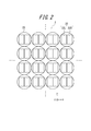
- FIG. 2 is a diagram illustrating a configuration of a main part of the image sensor.
- FIG. 3 is a horizontal sectional view of the image sensor.
- FIG. 4 is a diagram illustrating the arrangement of the imaging lens, the microlens, and the light receiving unit.
- FIG. 5 is a diagram illustrating the arrangement of the imaging lens, the microlens, and the light receiving unit.
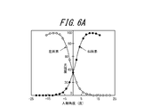
- FIG. 6A is a diagram illustrating the relationship between the incident angle to the light receiving unit and the signal light intensity in the case of the first embodiment.
- FIG. 1 is a block diagram illustrating a schematic configuration of the imaging apparatus according to the first embodiment.
- FIG. 2 is a diagram illustrating a configuration of a main part of the image sensor.
- FIG. 3 is a horizontal sectional view of the image sensor.
- FIG. 4 is a diagram illustrating the arrangement of the imaging lens, the microlens, and the
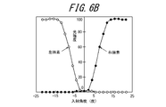
- FIG. 6B is a diagram illustrating the relationship between the incident angle to the light receiving unit and the signal light intensity when the pupil plane of the imaging lens and the light receiving surface of the light receiving unit are in a conjugate relationship.
- FIG. 7 is a diagram for explaining each parameter of the image sensor.
- FIG. 8 is a diagram illustrating the light intensity at the optical axis when crosstalk occurs.
- FIG. 9 is a plan view for explaining the configuration of the image sensor according to the second embodiment.
- FIG. 10 is a perspective view illustrating the configuration of the image sensor according to the second embodiment.
- FIG. 11 is a diagram illustrating a configuration of an image sensor according to the third embodiment.
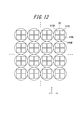
- FIG. 12 is a diagram illustrating the configuration of the image sensor according to the fourth embodiment.
- FIG. 1 is a block diagram illustrating a schematic configuration of an imaging apparatus according to the present embodiment.
- the imaging device 1 captures a parallax image for displaying a stereoscopic captured image based on the subject light 100 from the subject.
- the imaging device 1 includes an imaging lens 11, an imaging element 10, an image processing unit 12, a control unit 14, a storage unit 16, and a display unit 18.
- the image sensor 10, the image processing unit 12, the control unit 14, the storage unit 16, and the display unit 18 are connected to a bus 19 and configured to be able to transmit and receive various signals to and from each other.
- the imaging element 10 When the subject light 100 is incident through the imaging lens 11, the imaging element 10 captures a left-side-viewed captured image and a right-side-viewed captured image having parallax based on the subject light 100, and configures each captured image. A pixel signal is output.
- Each captured image is composed of pixels arranged two-dimensionally. The number of pixels constituting one frame of the captured image is, for example, 640 ⁇ 480 pixels to 4000 ⁇ 3000 pixels, but is not limited to this range.
- the image sensor 10 is a CMOS (Complementary Metal Metal Oxide Semiconductor) or a CCD (Charge Coupled Device) having light receiving elements arranged corresponding to each pixel, and generates and outputs pixel signals by the light receiving elements.
- CMOS Complementary Metal Metal Oxide Semiconductor
- CCD Charge Coupled Device
- the pixel signal is generated and output for each frame, for example.
- the pixel signal is a signal that indicates a gradation value of, for example, R (Red), G (Green), and B (Blue) for each pixel.
- the pixel signal is a digital signal obtained by A / D converting the output signal from the light receiving element, for example.
- the image processing unit 12 performs predetermined image processing such as color and luminance correction, distortion correction, and compression / decompression of data on captured image data including pixel signals for one frame. For example, the image processing unit 12 performs image processing on captured image data for each frame.
- the image processing unit 12 is a processor such as a DSP (Digital Signal Processor) or an ASIC (Application Specific Specific Integrated Circuit).
- the storage unit 16 is a frame memory that stores captured image data before and / or after image processing.
- the storage unit 16 is, for example, an SRAM (Static Random Access Memory) or a DRAM (Dynamic RAM).
- the storage unit 16 may include a data reading / writing device for various storage media including a hard disk and a portable flash memory.
- the display unit 18 displays a stereoscopic image based on the captured image data of the left visual field and the right visual field.
- the display unit 18 includes, for example, an LCD (Liquid Crystal Display) including a polarizing filter corresponding to the parallax between the left and right eyes and a control circuit thereof.
- the display unit 18 displays left and right captured image data having parallax, and displays a stereoscopic captured image that allows the user to perceive a stereoscopic effect.
- the control unit 14 sends control signals to the image sensor 10, the image processing unit 12, the storage unit 16, and the display unit 18, and controls the operation of the imaging device 1 in an integrated manner.
- the control unit 14 is a microcomputer, for example.
- FIG. 2 is a diagram for explaining a configuration of a main part of the image sensor 10.
- the image sensor 10 has a microlens array 2 composed of spherical microlenses 20 arranged two-dimensionally.
- the microlens 20 is disposed corresponding to one pixel of each image in the right field and the left field when capturing a parallax image.
- the X-axis direction corresponds to the left-right direction of the captured image
- the Y-axis direction corresponds to the vertical direction of the captured image
- the Z-axis direction corresponds to the optical axis direction.
- the image sensor 10 has two light receiving unit pairs 22 arranged for each microlens 20.
- the light receiving portions 22L and 22R of the light receiving portion pair 22 are, for example, photodiodes included in a CMOS or a CCD.
- Each of the light receiving units 22L and 22R generates and outputs a signal of a pixel (left pixel) that forms a captured image of the left visual field, and a signal of a pixel (right pixel) that configures the captured image of the right visual field.
- the right light receiving element 22R for generating and outputting.
- the light receiving portions 22L and 22R are disposed adjacent to each other in the X-axis direction, that is, in the left-right direction.
- Each of the light receiving units 22L and 22R corresponds to each pixel of a captured image pair for displaying a stereoscopic captured image.
- FIG. 3 is a cross-sectional view of the image sensor taken along the XZ plane (horizontal cross section).
- each microlens 20 is formed as an on-chip lens disposed in front of a pair of left and right light receiving portions 22L and 22R.
- the light receiving units 22L and 22R are driven and A wiring layer 23 for controlling or transmitting a signal is provided.
- the wiring layer 23 is made of a metal such as copper or aluminum, for example, and reflects or scatters light but does not transmit but functions as a light shielding layer.
- FIG. 4 is a diagram for explaining the arrangement of the imaging lens, the microlens of the imaging device, and the light receiving unit.
- the imaging lens 11 is configured by one lens or a combination of a plurality of lenses, and has a diaphragm 32.
- the optical axis 30 of the imaging lens 11 is arranged in parallel with the optical axis of each microlens 20.
- the light receiving elements 22L and 22R are disposed in the vicinity of the rear focal point where the light receiving surface 34 is shifted from the rear focal point of the microlens 20 by a predetermined distance.
- Many of recent imaging lenses for digital cameras are designed so that the position of the exit pupil is near infinity. Therefore, the image of the exit pupil of the imaging lens is formed on the pupil conjugate surface 36 near the light receiving surface 34 of the light receiving portions 22L and 22R through the microlens 20.
- FIG. 4 the light receiving surfaces 34 of the light receiving portions 22L and 22R are located on the object side relative to the image-side pupil conjugate surface 36 located conjugate with the pupil of the imaging lens 11.
- FIG. 5 is a diagram for explaining another arrangement of the imaging lens, the microlens of the imaging element, and the light receiving unit.
- the light receiving surfaces 34 of the light receiving portions 22L and 22R are located on the image side with respect to the image-side pupil conjugate surface 36 located at a conjugate position with the pupil of the imaging lens 11.
- the subject light 100 is condensed by the diaphragm 32, collected on the microlens array 20, and arranged between the microlens 20 and the light receiving units 22 ⁇ / b> L and 22 ⁇ / b> R. Detected by the light receiving portions 22L and 22R via the R, G and B color filters (not shown). R, G, or B light is incident on the light receiving portions 22L and 22R, and a subject image is formed.
- the light (left light flux) that has mainly passed through the left region of the pupil is incident on the left light receiving unit 22L, and generates a left pixel signal that forms a captured image of the left visual field.
- light (right light beam) that has mainly passed through the right region of the pupil is incident on the light receiving unit 22R, and generates a right pixel signal that forms a captured image of the right field of view.
- the pupil of the imaging lens 11 and the light receiving surfaces 34 of the light receiving portions 22L and 22R are out of the conjugate relationship, the object light 100 incident on the left light receiving portion 22L and the right eye light receiving portion 22R is not included. Crosstalk occurs between them.
- FIG. 6A and 6B are diagrams showing the relationship between the incident angle of the subject light to the image sensor and the signal light intensity of the left pixel signal and the right pixel signal.
- FIG. 6A is a diagram of FIG. 6B in the case of this embodiment. Shows a case where the pupil plane of the imaging lens and the light receiving surface of the light receiving element are in a conjugate relationship.
- the light receiving elements 22L and 22R have a certain degree of strength. Light is detected.
- the pupil plane of the imaging lens 11 and the light receiving surfaces 34 of the light receiving portions 22L and 22R are in a conjugate relationship, the left light receiving portion 22L and the right light receiving portion 22R are separated as shown in FIG. 6B. Although it is made, there is an angle range in which the left light receiving unit 22L and the right light receiving unit 22R almost do not detect light when the angle is around 0 degrees.
- the pupil of the imaging lens 11 and the light receiving surfaces 34 of the light receiving portions 22L and 22R deviate from the conjugate relationship as shown in FIG. 6A, signals with different fields of view are obtained for the left pixel and the right pixel, and acquisition of three-dimensional image information.
- a two-dimensional image is generated by adding the left pixel signal and the right pixel signal corresponding to each microlens 20, a natural image in which no double line appears can be generated.
- the focal length f L of the microlens 20 is It is represented by
- a part of the right beam in addition to most of the left beam enters the left light receiving unit 22L, and a part of the left beam in addition to most of the right beam enters the right light receiving unit 22R.
- the amount of light beams on the opposite side incident on the light receiving portions 22L and 22R is preferably 2% to 10% of the light amount of each light beam. That is, assuming that the pitch of the microlenses 20 is p, the blur width sb on the light receiving surface 34 of the light receiving portions 22L and 22R is: 0.02p ⁇ sb ⁇ 0.1p (2) It is desirable that
- the blur width sb on the light receiving surface 34 is: 0.02p + S ⁇ sb ⁇ 0.1p + S (3) Is desirable.
- Equation (3) The conditions for satisfying Equation (3) are examined below.
- the width of one blur of the light receiving portions 22L and 22R is set to h.
- sb 2h (4) It becomes.
- equation (3) 0.02p + S ⁇ 2h ⁇ 0.1p + S (5) It becomes.
- FIG. 8 is a diagram for explaining the light intensity at the optical axis when crosstalk occurs.
- the broken lines in FIG. 8 indicate the intensity of light received by the right light receiving unit 22R and the left light receiving unit 22L with respect to the incident angle of the subject light 100 when the shift amount is substantially 0 (that is, the right pixel signal and the left pixel signal). ing.
- the light intensity is shown as a ratio relative to the maximum value of the light intensity of the light beam as 100%. When the amount of deviation is 0, both the right beam and the left beam have values close to 0 near the incident angle of 0 degree.
- the solid line in FIG. 8 shows a case where the light receiving surface 34 is shifted from the focus of the microlens 20.
- the crosstalk portion in which the left light beam is received by the right light receiving element 22L is indicated by shading.
- the light intensity at an incident angle of 0 degree is about 20 to 30%. Therefore, when the signals of the right light receiving unit 22R and the left light receiving unit 22L are added to generate a two-dimensional image, the signal due to light incident from an incident angle of 0 degrees is also 40 to 60 compared with signals from other incident angles. % Intensity signal is obtained.
- the amount of light incident on the left and right light receiving portions 22L and 22R by the light beams on the left and right sides is 2% or more.
- the depth accuracy is determined by the amount of parallax, the pixel pitch, and the like.
- the amount of parallax when acquiring three-dimensional image information (depth information) by the pupil division method is defined by pupil diameter / 2. If the amount of crosstalk is 10%, the pupil diameter is reduced by 20%, and the depth resolution is reduced by 20%.
- the pupil diameter is 10 mm.
- the calculated parallax amount is 5 mm.
- the pitch of the image sensor 10 is 5 ⁇ m
- the depth resolution is 620 mm at a position where the distance from the optical system to the object (object distance) is 5 m.
- the crosstalk to the light receiving unit 22L or 22R on one side is 10% under the same conditions
- the pupil diameter is reduced by 20%, so that the parallax amount is 4 mm and the depth resolution is 745 mm. Since it is not preferable that the resolution is reduced by 20% or more, it is preferable that the amount of light incident on the left and right light receiving elements 22L and 22R is 10% or less.
- the parallax for generating a three-dimensional image In addition to obtaining an image, when creating a two-dimensional image, detection signals from the left-eye and right-eye light receiving elements 22L and 22R are added to obtain a more natural image.
- FIG. 9 is a plan view illustrating the configuration of the image sensor according to the second embodiment
- FIG. 10 is a perspective view illustrating the configuration of the image sensor according to the second embodiment.
- the left and right light receiving portions 22L and 22R are alternately arranged.
- a wiring layer 23 is provided between the light receiving portions 22L and 22R.
- a cylindrical lens 41 having an axis in the Y-axis direction is arranged above the light-receiving unit (in the Z-axis direction), and the left and right light-receiving units 22L and 22R have the same cylindrical lens. 41 is disposed below.
- a plurality of light receiving unit pairs 22 each including a set of left and right light receiving units 22L and 22R are arranged.
- the cylindrical lens 41 has a condensing function only in the X-axis direction, and the light receiving surfaces 34 of the light receiving elements 22L and 22R and the pupil of the imaging lens 11 are arranged out of a conjugate relationship. Since other configurations are the same as those of the first embodiment, the same or corresponding components are denoted by the same reference numerals and description thereof is omitted.
- the left luminous flux passing through the left side of the pupil of the imaging lens 11 and the right luminous flux passing through the right side of the subject light 100 are transmitted through the cylindrical lens 41, respectively. It can be detected by being incident on different left light receiving part 22L and right light receiving part 22R. Further, since the light receiving surfaces 34 of the light receiving portions 22L and 22R are arranged so as to be shifted from a position conjugate with the pupil of the imaging lens 11, the left light beam and the right light beam are partially partially in the right light receiving element 22R and the left light receiving portion, respectively. Incident on 22L.
- the pixel signals of the left pixel and the right pixel including the parallax information for generating the three-dimensional image are obtained, and by adding the pixel signals of the left pixel and the right pixel, a natural line with no double line appears.
- a two-dimensional image can be generated.
- FIG. 11 is a diagram illustrating a configuration of an image sensor according to the third embodiment.
- two light receiving elements are arranged for one microlens 20.
- the left light receiving unit 51L and the right light receiving unit 51R are arranged in the horizontal direction in which the subject image is formed, and the upper light receiving unit 51U and the lower light receiving unit 51D are arranged in the vertical direction.
- the light receiving surfaces 34 of these light receiving elements 51L, 51R, 51U, 51D are arranged at positions deviating from the conjugate relationship with the pupil of the imaging lens 11. Since other configurations are the same as those of the first embodiment, the same or corresponding components are denoted by the same reference numerals and description thereof is omitted.
- the present embodiment it is possible to pick up a parallax image for generating a three-dimensional image using the light receiving units 51L and 51R arranged in the horizontal direction, as in the first embodiment, and 2
- pixel signals from the left and right light receiving portions 51L and 51R are added to obtain a more natural image.
- depth information can be obtained from the parallax information in the vertical direction based on signals from the light receiving units 51U and 51D arranged in the vertical direction.
- the signals of the light receiving units 51U and 51D arranged in the vertical direction can be added together with the signal obtained by adding the light receiving units 51L and 51R arranged in the horizontal direction to create a two-dimensional image.
- FIG. 12 is a diagram illustrating the configuration of the image sensor 10 according to the third embodiment.
- a total of four light receiving portions 61DL, 61DR, 61UL, and 61UR are arranged in two rows in the horizontal direction and the vertical direction with respect to one microlens 20.
- each of the light receiving units 61DL, 61DR, 61UL, 61UR is divided into a lower left side, a lower right side, an upper left side, and an upper right side in the order when the pupil of the imaging lens 11 is divided into four by a horizontal straight line and a vertical straight line. It corresponds to the pupil.
- the light receiving surfaces 34 of these light receiving portions 61DL, 61DR, 61UL, 61UR are arranged at positions deviating from the conjugate relationship with the pupil of the imaging lens 11. Since other configurations are the same as those of the first embodiment, the same or corresponding components are denoted by the same reference numerals and description thereof is omitted.
- a stereoscopic image is generated based on pixel signals output from the left and right pixel pairs of the image sensor 10, that is, the light receiving units 61DL and 61DR and / or 61UL and 61UR. It is possible to generate a pixel signal of a two-dimensional image by adding the signals of the light receiving units 61DL, 61DR, 61UL, and 61UR corresponding to one microlens 20, and a two-dimensional image can be generated. As a result, the same effect as in the first embodiment can be obtained.
- vertical parallax information can also be obtained based on pixel signals output from the upper and lower pixel pairs of the image sensor 10, that is, the light receiving portions 61DL and 61UL and / or 61UR and 61UR. Accordingly, it is possible to obtain vertical and horizontal parallax information while using the same image sensor.
- the present invention is not limited to the above embodiment, and many variations or modifications are possible.
- the number of light receiving units for one microlens is not limited to two or four.
- the direction of the arrangement of the light receiving elements is not limited to the left and right and the top and bottom. For example, you may have the light receiving element pair arranged in the diagonal direction.
- the display unit does not necessarily have to be integrated with the imaging device, and may be provided as separate hardware for displaying a three-dimensional image.
Landscapes
- Engineering & Computer Science (AREA)
- Multimedia (AREA)
- Signal Processing (AREA)
- Physics & Mathematics (AREA)
- General Physics & Mathematics (AREA)
- Optics & Photonics (AREA)
- Testing, Inspecting, Measuring Of Stereoscopic Televisions And Televisions (AREA)
- Transforming Light Signals Into Electric Signals (AREA)
- Studio Devices (AREA)
- Stereoscopic And Panoramic Photography (AREA)
Priority Applications (3)
| Application Number | Priority Date | Filing Date | Title |
|---|---|---|---|
| US14/534,742 US9190436B2 (en) | 2012-11-08 | 2014-11-06 | Imaging apparatus |
| US14/918,973 US9305957B2 (en) | 2012-11-08 | 2015-10-21 | Imaging apparatus |
| US15/058,856 US9419037B2 (en) | 2012-11-08 | 2016-03-02 | Imaging apparatus |
Applications Claiming Priority (2)
| Application Number | Priority Date | Filing Date | Title |
|---|---|---|---|
| JP2012246651A JP5584270B2 (ja) | 2012-11-08 | 2012-11-08 | 撮像装置 |
| JP2012-246651 | 2012-11-08 |
Related Child Applications (1)
| Application Number | Title | Priority Date | Filing Date |
|---|---|---|---|
| US14/534,742 Continuation US9190436B2 (en) | 2012-11-08 | 2014-11-06 | Imaging apparatus |
Publications (1)
| Publication Number | Publication Date |
|---|---|
| WO2014073172A1 true WO2014073172A1 (ja) | 2014-05-15 |
Family
ID=50684298
Family Applications (1)
| Application Number | Title | Priority Date | Filing Date |
|---|---|---|---|
| PCT/JP2013/006242 Ceased WO2014073172A1 (ja) | 2012-11-08 | 2013-10-22 | 撮像装置 |
Country Status (3)
| Country | Link |
|---|---|
| US (3) | US9190436B2 (enExample) |
| JP (1) | JP5584270B2 (enExample) |
| WO (1) | WO2014073172A1 (enExample) |
Families Citing this family (6)
| Publication number | Priority date | Publication date | Assignee | Title |
|---|---|---|---|---|
| US10148864B2 (en) | 2015-07-02 | 2018-12-04 | Pixart Imaging Inc. | Imaging device having phase detection pixels and regular pixels, and operating method thereof |
| US9978154B2 (en) * | 2015-07-02 | 2018-05-22 | Pixart Imaging Inc. | Distance measurement device base on phase difference and distance measurement method thereof |
| US10403668B2 (en) * | 2015-07-29 | 2019-09-03 | Samsung Electronics Co., Ltd. | Imaging apparatus and image sensor including the same |
| US10790325B2 (en) | 2015-07-29 | 2020-09-29 | Samsung Electronics Co., Ltd. | Imaging apparatus and image sensor including the same |
| US11469265B2 (en) | 2015-07-29 | 2022-10-11 | Samsung Electronics Co., Ltd. | Imaging apparatus and image sensor including the same |
| US11089286B2 (en) | 2015-07-29 | 2021-08-10 | Samsung Electronics Co., Ltd. | Image sensor |
Citations (2)
| Publication number | Priority date | Publication date | Assignee | Title |
|---|---|---|---|---|
| JP2008015215A (ja) * | 2006-07-06 | 2008-01-24 | Nikon Corp | 固体撮像素子及びこれを用いた撮像装置 |
| JP2010102230A (ja) * | 2008-10-27 | 2010-05-06 | Nikon Corp | カメラレンズアダプタ及びカメラシステム |
Family Cites Families (9)
| Publication number | Priority date | Publication date | Assignee | Title |
|---|---|---|---|---|
| US6396873B1 (en) | 1999-02-25 | 2002-05-28 | Envision Advanced Medical Systems | Optical device |
| WO2007011026A1 (ja) * | 2005-07-22 | 2007-01-25 | Nikon Corporation | 撮像素子、焦点検出装置および撮像システム |
| US20090219432A1 (en) | 2008-02-29 | 2009-09-03 | Palum Russell J | Sensor with multi-perspective image capture |
| EP2146248B1 (en) * | 2008-07-16 | 2012-08-29 | Carl Zeiss SMT GmbH | Illumination system of a microlithographic projection exposure apparatus |
| US8749620B1 (en) * | 2010-02-20 | 2014-06-10 | Lytro, Inc. | 3D light field cameras, images and files, and methods of using, operating, processing and viewing same |
| JP5513326B2 (ja) * | 2010-09-07 | 2014-06-04 | キヤノン株式会社 | 撮像素子及び撮像装置 |
| JP5864990B2 (ja) * | 2011-10-03 | 2016-02-17 | キヤノン株式会社 | 固体撮像装置およびカメラ |
| JP5743837B2 (ja) * | 2011-10-07 | 2015-07-01 | キヤノン株式会社 | 光電変換装置、撮像装置および撮像システム |
| JP5818697B2 (ja) * | 2012-01-13 | 2015-11-18 | キヤノン株式会社 | 画像生成方法、撮像装置および表示装置、プログラム、記憶媒体 |
-
2012
- 2012-11-08 JP JP2012246651A patent/JP5584270B2/ja not_active Expired - Fee Related
-
2013
- 2013-10-22 WO PCT/JP2013/006242 patent/WO2014073172A1/ja not_active Ceased
-
2014
- 2014-11-06 US US14/534,742 patent/US9190436B2/en not_active Expired - Fee Related
-
2015
- 2015-10-21 US US14/918,973 patent/US9305957B2/en not_active Expired - Fee Related
-
2016
- 2016-03-02 US US15/058,856 patent/US9419037B2/en not_active Expired - Fee Related
Patent Citations (2)
| Publication number | Priority date | Publication date | Assignee | Title |
|---|---|---|---|---|
| JP2008015215A (ja) * | 2006-07-06 | 2008-01-24 | Nikon Corp | 固体撮像素子及びこれを用いた撮像装置 |
| JP2010102230A (ja) * | 2008-10-27 | 2010-05-06 | Nikon Corp | カメラレンズアダプタ及びカメラシステム |
Also Published As
| Publication number | Publication date |
|---|---|
| JP5584270B2 (ja) | 2014-09-03 |
| US9419037B2 (en) | 2016-08-16 |
| US20150061066A1 (en) | 2015-03-05 |
| JP2014096683A (ja) | 2014-05-22 |
| US20160181300A1 (en) | 2016-06-23 |
| US9190436B2 (en) | 2015-11-17 |
| US9305957B2 (en) | 2016-04-05 |
| US20160043124A1 (en) | 2016-02-11 |
Similar Documents
| Publication | Publication Date | Title |
|---|---|---|
| US9851483B2 (en) | Stereoscopic imaging method and system that divides a pixel matrix into subgroups | |
| US9036004B2 (en) | Three-dimensional image capture device | |
| JP5982751B2 (ja) | 画像処理装置、および画像処理方法、並びにプログラム | |
| EP2579568B1 (en) | Imaging device and imaging method | |
| US20120112037A1 (en) | Three-dimensional imaging device | |
| JPWO2012042963A1 (ja) | 固体撮像素子及び撮像装置 | |
| US20120105598A1 (en) | Three-dimensional imaging device | |
| JP5584270B2 (ja) | 撮像装置 | |
| CN104185983B (zh) | 摄像元件、摄像装置以及摄像系统 | |
| CN104041006B (zh) | 图像生成方法以及图像生成设备 | |
| CN105359519B (zh) | 摄像装置 | |
| WO2012169301A1 (ja) | 立体動画像及び平面動画像を撮像する撮像素子及びこの撮像素子を搭載する撮像装置 | |
| JP5810196B2 (ja) | 撮像装置 | |
| CN103907188B (zh) | 摄像元件、摄像装置及图像处理装置 | |
| JP6234024B2 (ja) | 撮像素子、及び撮像装置 | |
| WO2012153504A1 (ja) | 撮像装置および撮像装置の制御プログラム | |
| JP6086681B2 (ja) | 撮像素子、及び撮像装置 | |
| JP2014103427A (ja) | 立体画像撮像装置 | |
| JP2013239787A (ja) | 撮像素子及びこれを用いた撮像装置 | |
| JP5452800B2 (ja) | 立体像撮影装置 | |
| JP5853510B2 (ja) | 撮像装置 | |
| JP6331279B2 (ja) | 撮像装置、撮像方法およびプログラム |
Legal Events
| Date | Code | Title | Description |
|---|---|---|---|
| 121 | Ep: the epo has been informed by wipo that ep was designated in this application |
Ref document number: 13853915 Country of ref document: EP Kind code of ref document: A1 |
|
| NENP | Non-entry into the national phase |
Ref country code: DE |
|
| 122 | Ep: pct application non-entry in european phase |
Ref document number: 13853915 Country of ref document: EP Kind code of ref document: A1 |