US11089286B2 - Image sensor - Google Patents
Image sensor Download PDFInfo
- Publication number
- US11089286B2 US11089286B2 US16/284,087 US201916284087A US11089286B2 US 11089286 B2 US11089286 B2 US 11089286B2 US 201916284087 A US201916284087 A US 201916284087A US 11089286 B2 US11089286 B2 US 11089286B2
- Authority
- US
- United States
- Prior art keywords
- scatterers
- light
- wavelength
- image sensor
- thin
- Prior art date
- Legal status (The legal status is an assumption and is not a legal conclusion. Google has not performed a legal analysis and makes no representation as to the accuracy of the status listed.)
- Active, expires
Links
Images


Classifications
-
- H—ELECTRICITY
- H04—ELECTRIC COMMUNICATION TECHNIQUE
- H04N—PICTORIAL COMMUNICATION, e.g. TELEVISION
- H04N13/00—Stereoscopic video systems; Multi-view video systems; Details thereof
- H04N13/20—Image signal generators
- H04N13/204—Image signal generators using stereoscopic image cameras
- H04N13/207—Image signal generators using stereoscopic image cameras using a single two-dimensional [2D] image sensor
- H04N13/229—Image signal generators using stereoscopic image cameras using a single two-dimensional [2D] image sensor using lenticular lenses, e.g. arrangements of cylindrical lenses
-
- G—PHYSICS
- G02—OPTICS
- G02B—OPTICAL ELEMENTS, SYSTEMS OR APPARATUS
- G02B3/00—Simple or compound lenses
- G02B3/0006—Arrays
- G02B3/0037—Arrays characterized by the distribution or form of lenses
- G02B3/0043—Inhomogeneous or irregular arrays, e.g. varying shape, size, height
-
- G—PHYSICS
- G02—OPTICS
- G02B—OPTICAL ELEMENTS, SYSTEMS OR APPARATUS
- G02B3/00—Simple or compound lenses
- G02B3/02—Simple or compound lenses with non-spherical faces
- G02B3/08—Simple or compound lenses with non-spherical faces with discontinuous faces, e.g. Fresnel lens
-
- G—PHYSICS
- G02—OPTICS
- G02B—OPTICAL ELEMENTS, SYSTEMS OR APPARATUS
- G02B5/00—Optical elements other than lenses
- G02B5/18—Diffraction gratings
- G02B5/1876—Diffractive Fresnel lenses; Zone plates; Kinoforms
- G02B5/188—Plurality of such optical elements formed in or on a supporting substrate
-
- G—PHYSICS
- G02—OPTICS
- G02B—OPTICAL ELEMENTS, SYSTEMS OR APPARATUS
- G02B5/00—Optical elements other than lenses
- G02B5/20—Filters
- G02B5/201—Filters in the form of arrays
-
- H01L27/14605—
-
- H01L27/14621—
-
- H01L27/14627—
-
- H—ELECTRICITY
- H04—ELECTRIC COMMUNICATION TECHNIQUE
- H04N—PICTORIAL COMMUNICATION, e.g. TELEVISION
- H04N13/00—Stereoscopic video systems; Multi-view video systems; Details thereof
- H04N13/20—Image signal generators
- H04N13/204—Image signal generators using stereoscopic image cameras
- H04N13/207—Image signal generators using stereoscopic image cameras using a single two-dimensional [2D] image sensor
- H04N13/214—Image signal generators using stereoscopic image cameras using a single two-dimensional [2D] image sensor using spectral multiplexing
-
- H—ELECTRICITY
- H04—ELECTRIC COMMUNICATION TECHNIQUE
- H04N—PICTORIAL COMMUNICATION, e.g. TELEVISION
- H04N13/00—Stereoscopic video systems; Multi-view video systems; Details thereof
- H04N13/20—Image signal generators
- H04N13/271—Image signal generators wherein the generated image signals comprise depth maps or disparity maps
-
- H—ELECTRICITY
- H10—SEMICONDUCTOR DEVICES; ELECTRIC SOLID-STATE DEVICES NOT OTHERWISE PROVIDED FOR
- H10F—INORGANIC SEMICONDUCTOR DEVICES SENSITIVE TO INFRARED RADIATION, LIGHT, ELECTROMAGNETIC RADIATION OF SHORTER WAVELENGTH OR CORPUSCULAR RADIATION
- H10F39/00—Integrated devices, or assemblies of multiple devices, comprising at least one element covered by group H10F30/00, e.g. radiation detectors comprising photodiode arrays
- H10F39/80—Constructional details of image sensors
- H10F39/802—Geometry or disposition of elements in pixels, e.g. address-lines or gate electrodes
- H10F39/8023—Disposition of the elements in pixels, e.g. smaller elements in the centre of the imager compared to larger elements at the periphery
-
- H—ELECTRICITY
- H10—SEMICONDUCTOR DEVICES; ELECTRIC SOLID-STATE DEVICES NOT OTHERWISE PROVIDED FOR
- H10F—INORGANIC SEMICONDUCTOR DEVICES SENSITIVE TO INFRARED RADIATION, LIGHT, ELECTROMAGNETIC RADIATION OF SHORTER WAVELENGTH OR CORPUSCULAR RADIATION
- H10F39/00—Integrated devices, or assemblies of multiple devices, comprising at least one element covered by group H10F30/00, e.g. radiation detectors comprising photodiode arrays
- H10F39/80—Constructional details of image sensors
- H10F39/805—Coatings
- H10F39/8053—Colour filters
-
- H—ELECTRICITY
- H10—SEMICONDUCTOR DEVICES; ELECTRIC SOLID-STATE DEVICES NOT OTHERWISE PROVIDED FOR
- H10F—INORGANIC SEMICONDUCTOR DEVICES SENSITIVE TO INFRARED RADIATION, LIGHT, ELECTROMAGNETIC RADIATION OF SHORTER WAVELENGTH OR CORPUSCULAR RADIATION
- H10F39/00—Integrated devices, or assemblies of multiple devices, comprising at least one element covered by group H10F30/00, e.g. radiation detectors comprising photodiode arrays
- H10F39/80—Constructional details of image sensors
- H10F39/806—Optical elements or arrangements associated with the image sensors
- H10F39/8063—Microlenses
-
- G—PHYSICS
- G03—PHOTOGRAPHY; CINEMATOGRAPHY; ANALOGOUS TECHNIQUES USING WAVES OTHER THAN OPTICAL WAVES; ELECTROGRAPHY; HOLOGRAPHY
- G03B—APPARATUS OR ARRANGEMENTS FOR TAKING PHOTOGRAPHS OR FOR PROJECTING OR VIEWING THEM; APPARATUS OR ARRANGEMENTS EMPLOYING ANALOGOUS TECHNIQUES USING WAVES OTHER THAN OPTICAL WAVES; ACCESSORIES THEREFOR
- G03B35/00—Stereoscopic photography
- G03B35/08—Stereoscopic photography by simultaneous recording
- G03B35/10—Stereoscopic photography by simultaneous recording having single camera with stereoscopic-base-defining system
-
- H—ELECTRICITY
- H04—ELECTRIC COMMUNICATION TECHNIQUE
- H04N—PICTORIAL COMMUNICATION, e.g. TELEVISION
- H04N13/00—Stereoscopic video systems; Multi-view video systems; Details thereof
- H04N13/20—Image signal generators
- H04N13/204—Image signal generators using stereoscopic image cameras
- H04N13/207—Image signal generators using stereoscopic image cameras using a single two-dimensional [2D] image sensor
- H04N13/232—Image signal generators using stereoscopic image cameras using a single two-dimensional [2D] image sensor using fly-eye lenses, e.g. arrangements of circular lenses
-
- H—ELECTRICITY
- H04—ELECTRIC COMMUNICATION TECHNIQUE
- H04N—PICTORIAL COMMUNICATION, e.g. TELEVISION
- H04N2213/00—Details of stereoscopic systems
- H04N2213/001—Constructional or mechanical details
-
- H—ELECTRICITY
- H04—ELECTRIC COMMUNICATION TECHNIQUE
- H04N—PICTORIAL COMMUNICATION, e.g. TELEVISION
- H04N23/00—Cameras or camera modules comprising electronic image sensors; Control thereof
- H04N23/57—Mechanical or electrical details of cameras or camera modules specially adapted for being embedded in other devices
-
- H04N5/2257—
Definitions
- Apparatuses and methods consistent with exemplary embodiments relate to image sensors.
- Optical sensors including semiconductor sensor arrays may be used in mobile devices, wearable devices, and the Internet of Things. Although such devices should be small, it is difficult to reduce the thicknesses of imaging apparatuses included in these devices.
- Exemplary embodiments may address at least the above problems and/or disadvantages and other disadvantages not described above. Also, the exemplary embodiments are not required to overcome the disadvantages described above, and may not overcome any of the problems described above.
- image sensors may be configured to have a small size and may be configured to obtain 3-dimensional information about an object.
- an image sensor includes an image sensor includes a substrate, thin lenses disposed on a first surface of the substrate and configured to concentrate lights incident on the first surface, and light-sensing cells disposed on a second surface of the substrate, the second surface facing the first surface, and the light-sensing cells being configured to sense lights passing through the thin lenses, and generate electrical signals based on the sensed lights.
- a first thin lens and second thin lens of the thin lenses are configured to concentrate a first light and a second light, respectively, of the incident lights onto the light-sensing cells, the first light having a different wavelength than the second light.
- the substrate may include sub-substrates, and the thin lenses and the light-sensing cells may be respectively disposed on a first surface and a second surface of each of the sub-substrates.
- Each of the thin lenses may include scatterers, and each of the scatterers may have a pillar structure.
- An interval distance between a pair of the scatterers may be less than a respective wavelength of light concentrated by a respective one among the thin lenses.
- a height of the scatterers may be less than a respective wavelength of light concentrated by a respective one among the thin lenses.
- the scatterers may include at least one from among silicon, gallium phosphide, SiC, SiN, and TiO 2 .
- Shapes of the scatterers and interval distances between respective pairs of the scatterers may vary with a respective wavelength of light concentrated by a respective one among the thin lenses.
- the image sensor may further include light filters, each of the light filters being configured to filter a respective wavelength of light incident on a respective one among the light-sensing cells.
- the image sensor may further include an image synthesizer configured to generate a multi-color image by synthesizing images of different colors, and at least two among the light-sensing cells may produce the images of different colors.
- an image synthesizer configured to generate a multi-color image by synthesizing images of different colors, and at least two among the light-sensing cells may produce the images of different colors.
- the image sensor may further include an image synthesizer configured to generate a stereo image based on images that are produced by the light-sensing cells.
- the image synthesizer may be further configured to extract depth information about an object appearing in the stereo image.
- an image sensor includes a substrate, thin lenses disposed on a first surface of the substrate and configured to concentrate lights incident on the first surface, and light-sensing cells disposed on a second surface of the substrate, the second surface facing the first surface, and the light-sensing cells being configured to sense lights passing through the thin lenses, and generate electrical signals based on the sensed lights.
- a first thin lens and second thin lens of the thin lenses may be configured to concentrate a first light and a second light, respectively, of the incident lights to have different focal lengths.
- the substrate may include sub-substrates, and the thin lenses and the light-sensing cells may be respectively disposed on a first surface and a second surface of each of the sub-substrates.
- the concentrated lights may have predetermined wavelengths.
- Each of the thin lenses may include scatterers, and each of the scatterers may have a pillar structure.
- An interval distance between a pair of the scatterers may be less than a respective wavelength of light concentrated by a respective one among the thin lenses.
- a height of the scatterers may be less than a respective wavelength of light concentrated by a respective one among the thin lenses.
- Shapes of the scatterers and interval distances between respective pairs of the scatterers may vary with a respective wavelength of light concentrated by a respective one among the thin lenses.
- the image sensor may further include a depth map calculator configured to calculate a defocusing degree of an image that is produced on each of the light-sensing cells, and calculate depth map information about an image that is produced by the incident lights, based on the defocusing degree.
- a depth map calculator configured to calculate a defocusing degree of an image that is produced on each of the light-sensing cells, and calculate depth map information about an image that is produced by the incident lights, based on the defocusing degree.
- the image sensor may further include a light filter layer configured to filter a wavelength of light incident on each of the light-sensing cells.
- an image sensor includes a substrate, a first thin lens configured to concentrate light of a first wavelength, and including a plurality of first scatterers disposed on the substrate.
- the plurality of first scatterers includes a material having a refractive index greater than a refractive index of the substrate.
- the image sensor further includes a plurality of light-sensing cells configured to sense the light concentrated by the first thin lens.
- the image sensor may further include a housing configured to fix the first thin lens and the plurality of light-sensing cells, while maintaining a distance between the first thin lens and the plurality of light-sensing cells.
- the image sensor may further include a low-refractive index material layer covering the plurality of first scatterers, and including a material having a refractive index less than the refractive index of the material of the plurality of first scatterers.
- the first thin lens further may include a plurality of second scatterers disposed on the low-refractive index material layer and including a material having a refractive index greater than the refractive index of the material of the low-refractive index material layer.
- Each of the plurality of first scatterers and the plurality of second scatterers may have a pillar shape.
- Each of the plurality of first scatterers and the plurality of second scatterers may have a shape dimension less than the first wavelength.
- Each of a distance between the plurality of first scatterers and a distance between the second scatterers may be less than the first wavelength.
- the image sensor may further include a second thin lens configured to concentrate light of a second wavelength different from the first wavelength, and including a plurality of third scatterers disposed on the substrate, and including a material having a refractive index greater than the refractive index of the substrate, and a plurality of fourth scatterers disposed on a layer different from the plurality of third scatterers, and spaced apart from the third scatterers.
- a second thin lens configured to concentrate light of a second wavelength different from the first wavelength, and including a plurality of third scatterers disposed on the substrate, and including a material having a refractive index greater than the refractive index of the substrate, and a plurality of fourth scatterers disposed on a layer different from the plurality of third scatterers, and spaced apart from the third scatterers.
- Each of the plurality of third scatterers and the plurality of fourth scatterers may have shape dimension less than the second wavelength.
- Each of a distance between the plurality of third scatterers and a distance between the plurality of fourth scatterers may be less than the second wavelength.
- the low-refractive index material layer may be covering the plurality of third scatterers, and the plurality of fourth scatterers may be disposed on the low-refractive material layer.
- a shape distribution of the plurality of first scatterers and the plurality of second scatterers included in the first thin lens may be different from a shape distribution of the plurality of third scatterers and the plurality of fourth scatterers included in the second thin lens.
- the image sensor may further include an optical filter configured to filter incident light such that the light of the first wavelength and the light of the second wavelength are respectively incident on the first thin lens and the second thin lens.
- the image sensor may further include a second thin lens configured to concentrate the light of the first wavelength, and having a focal length different from a focal length of the first thin lens
- the second thin lens may include a plurality of third scatterers disposed on the substrate, and including a material having a refractive index greater than the refractive index of the substrate, and a plurality of fourth scatterers disposed on a layer different from the plurality of third scatterers, and spaced apart from the third scatterers.
- the image sensor may further include a depth map calculator configured to calculate a defocusing degree of the light concentrated by the first thin lens and the light concentrated by the second thin lens that are sensed by the plurality of light-sensing cells and calculate depth map information of an image that is represented by the light concentrated by the first thin lens and the light concentrated by the second thin lens that are sensed by the plurality of light-sensing cells, based on the calculated defocusing degree.
- a depth map calculator configured to calculate a defocusing degree of the light concentrated by the first thin lens and the light concentrated by the second thin lens that are sensed by the plurality of light-sensing cells and calculate depth map information of an image that is represented by the light concentrated by the first thin lens and the light concentrated by the second thin lens that are sensed by the plurality of light-sensing cells, based on the calculated defocusing degree.
- the image sensor may further include a third thin lens configured to concentrate light having a second wavelength different from the first wavelength, and including a plurality of fifth scatterers disposed on the substrate, and including a material having a refractive index greater than the refractive index of the substrate, and a plurality of sixth scatterers disposed on a layer different from the plurality of third scatterers, and spaced apart from the fifth scatterers.
- a third thin lens configured to concentrate light having a second wavelength different from the first wavelength, and including a plurality of fifth scatterers disposed on the substrate, and including a material having a refractive index greater than the refractive index of the substrate, and a plurality of sixth scatterers disposed on a layer different from the plurality of third scatterers, and spaced apart from the fifth scatterers.
- Each of the plurality of fifth scatterers and the plurality of sixth scatterers may have a shape dimension less than the second wavelength.
- Each of a distance between the plurality of fifth scatterers and a distance between the sixth scatterers may be less than the second wavelength.
- a shape distribution of the plurality of fifth scatterers and the plurality of sixth scatterers included in the third thin lens may be different from a shape distribution of the plurality of first scatterers and the plurality of second scatterers included in the first thin lens and from a shape distribution of the plurality of third scatterers and the plurality of fourth scatterers included in the second thin lens.
- the image sensor may further include a fourth thin lens configured to concentrate the light of the second wavelength, and having a focal length different from a focal length of the third thin lens.
- the second thin lens may include a plurality of seventh scatterers disposed on the substrate, and including a material having a refractive index greater than the refractive index of the substrate, and a plurality of eighth scatterers disposed on a layer different from the plurality of seventh scatterers, and spaced apart from the seventh scatterers.
- a shape distribution of the plurality of seventh scatterers and the plurality of eighth scatterers included in the fourth thin lens may be different from a shape distribution of the plurality of fifth scatterers and the plurality of sixth scatterers included in the third thin lens.
- FIG. 1 is a cross-sectional view illustrating an image sensor according to an exemplary embodiment
- FIG. 2 is a view illustrating a surface of a thin lens according to an exemplary embodiment
- FIGS. 3A, 3B, 3C, and 3D are perspective views illustrating various shapes of scatterers according to exemplary embodiments
- FIG. 4 is a view of a surface illustrating a first thin lens according to an exemplary embodiment
- FIG. 5 is a view illustrating a surface of a first thin lens according to another exemplary embodiment
- FIG. 6 is a view illustrating an image sensor according to an exemplary embodiment
- FIG. 7 is a view illustrating an image sensor according to an exemplary embodiment
- FIG. 8 is a view illustrating an image sensor according to an exemplary embodiment
- FIG. 9 is a view illustrating an image sensor according to another exemplary embodiment.
- FIG. 10 is a view illustrating an image sensor including a substrate including a plurality of sub-substrates, according to an exemplary embodiment
- FIG. 11 is a view illustrating an image sensor according to an exemplary embodiment
- FIG. 12 is a view illustrating an image sensor according to an exemplary embodiment.
- FIG. 13 is a view illustrating an image sensor according to an exemplary embodiment.
- FIG. 14 is a cross-sectional view illustrating an image sensor according to another exemplary embodiment
- FIG. 15 is a cross-sectional view of a thin lens that is included in an image sensor according to another exemplary embodiment.
- FIG. 16 is a graph illustrating a function of the thin lens of FIG. 15 that focuses light of a wavelength.
- FIG. 17 is a cross-sectional view illustrating an image sensor according to another exemplary embodiment.
- FIG. 18 is a cross-sectional view illustrating an image sensor according to another exemplary embodiment.
- FIG. 19 is a cross-sectional view illustrating an image sensor according to another exemplary embodiment.
- the term “and/or” includes any and all combinations of one or more of the associated listed items. Expressions such as “at least one of,” when preceding a list of elements, modify the entire list of elements and do not modify the individual elements of the list.
- FIG. 1 is a cross-sectional view illustrating an image sensor according to an exemplary embodiment.
- the image sensor may include a substrate 110 , a plurality of thin lenses 120 a , 120 b , and 120 c that are arranged on a first surface S 1 , and a plurality of light-sensing cells 130 a , 130 b , and 130 c arranged on a second surface S 1 facing the first surface S 1 of the substrate 110 .
- At least two from among the thin lenses 120 a , 120 b , and 120 c may concentrate lights having different wavelength components on the light-sensing cells 130 a , 130 b , and 130 c . That is, two or more of the thin lenses 120 a , 120 b , and 120 c may have wavelength selectivity with respect to different wavelengths.
- the substrate 110 may have a plate-like shape.
- the first surface S 1 and the second surface S 2 of the substrate 110 may be substantially horizontally parallel to each other. However, the first surface S 1 and the second surface S 2 may not be completely horizontally parallel to each other and may be obliquely parallel to each other.
- the substrate 110 and the light-sensing cells 130 a , 130 b , and 130 c may be spaced apart from one another with an air layer therebetween.
- the substrate 110 may include a transparent material.
- the term “transparent material” denotes a material having a high light transmittance.
- the substrate 110 may include at least one from among Si 3 N 4 , SiO 2 , and a polymer such as PMMA or PDMS.
- Each of the light-sensing cells 130 a , 130 b , and 130 c may include scatterers from among a plurality of scatterers 122 a , 122 b , and 122 c .
- the term ‘thin-lens’ refers to an optical device that changes a path of light by a difference in phase delays caused by the scatterers 122 a , 122 b , and 122 c included in the thin-lenses, unlike related art optical lens. Accordingly, a thickness of the thin-lens may be hardly limited compared to that of an optical lens, and the thin-lens may be configured to be thin.
- the scatterers 122 a , 122 b , and 122 c on surfaces of the thin lenses 120 a , 120 b , and 120 c may be configured to resonate light incident on each of the scatterers 122 a , 122 b , and 122 c .
- the scatterers 122 a , 122 b , and 122 c may be configured to appropriately delay a transmission phase of the light incident on each of the scatterers 122 a , 122 b , and 122 c.
- the scatterers 122 a , 122 b , and 122 c may be arranged on the first surface S 1 of the substrate 110 to form a desired wave front of light that transmits from the first surface S 1 of the substrate 110 . Also, the thin lenses 120 a , 120 b , and 120 c may change a path of transmittant light with respect to incident light by modulating a wave front of light.
- At least two from among the thin lenses 120 a , 120 b , and 120 c may be configured to concentrate pieces of light having different wavelength components among the incident light on the light sensing layer 130 .
- a first thin-lens 120 a may be configured to concentrate a piece of light having a first wavelength ⁇ 1 among the incident light.
- a second thin-lens 120 b may be configured to concentrate a piece of light having a second wavelength ⁇ 2 among the incident light.
- a third thin-lens 120 c may be configured to concentrate a piece of light having a third wavelength ⁇ 3 among the incident light.
- these are provided as examples for illustrative purpose only, and embodiments are not limited thereto.
- not all of the first to third thin lenses 120 a , 120 b , and 120 c have to concentrate pieces of light having different wavelengths, and two from among the first, second, and third thin lenses 120 a , 120 b , and 120 c may be configured to concentrate pieces of light having substantially the same wavelength.
- FIG. 2 is a view illustrating a surface of one from among the thin lenses 120 a , 120 b , and 120 c according to an exemplary embodiment.
- a plurality of scatterers may be arranged on a surface of a thin-lens.
- a wave form of light transmitted from the thin-lens may depend on a shape, an interval distance, and a shape of arrangement of the scatterers.
- the scatterers When the scatterers are formed on the surface of the thin-lens as shown in FIG. 2 , light transmitted from the thin-lens may be concentrated. That is, the thin-lens shown in FIG. 2 may be configured as a lens having positive refractive power.
- FIGS. 3A, 3B, 3C, and 3D are perspective views illustrating various shapes of the scatterers 122 a , 122 b , and 122 c according to exemplary embodiments.
- the scatterers 122 a , 122 b , and 122 c included in the thin lenses 120 a , 120 b , and 120 c may have pillar structures.
- a shape of a cross-section of the pillar structure may be from among a circle, an oval, a rectangle, and a square.
- FIG. 3A illustrates a scatterer having a pillar structure with a cross-sectional shape of a circle.
- FIG. 3B illustrates a scatterer having a pillar structure with a cross-sectional shape of an oval.
- FIG. 3C illustrates a scatterer having a pillar structure with a cross-sectional shape of a square.
- FIG. 3D illustrates a scatterer having a pillar structure with a cross-sectional shape of a rectangle.
- the pillar structure may be appropriately tilted in a height direction.
- FIGS. 3A through 3D show examples of shapes of the scatterers 122 a , 122 b , and 122 c , but embodiments are not limited thereto.
- at least one from among the scatterers 122 a , 122 b , and 122 c may have a polygonal prism shape or a pillar structure with a cross-section having an “L”-like shape.
- At least one from among the scatterers 122 a , 122 b , and 122 c may have a multi-layer structure formed of materials with different refractive indexes in a height direction.
- shapes of the scatterers 122 a , 122 b , and 122 c may not have symmetricity in a direction.
- a cross-section of the scatterers 122 a , 122 b , and 122 c may have shapes that are non-symmetrical in a horizontal direction such as, for example, an oval shape. Also, when cross-sections of the scatterers 122 a , 122 b , and 122 c differ according to their height, the shapes of the scatterers 122 a , 122 b , and 122 c may not have symmetricity with respect to the height.
- the scatterers 122 a , 122 b , and 122 c may have a shape according to wavelength selectivity of the thin lenses 120 a , 120 b , and 120 c .
- the term “wavelength selectivity” refers to each of the thin lenses 120 a , 120 b , and 120 c selectively concentrating pieces of light of a predetermined wavelength band on the light sensing layer 130 .
- the scatterers 122 a included in the first thin-lens 120 a may have a shape appropriate to concentrate pieces of light of the first wavelength ⁇ 1 .
- a cross-sectional shape of scatterers 122 a and a ratio between a width and a height of the scatterers 122 a may change.
- scatterers 122 b included in the second thin-lens 120 b may have a shape appropriate to concentrate pieces of light of the second wavelength ⁇ 2 .
- scatterers 122 c included in the third thin-lens 120 c may have a shape appropriate to concentrate pieces of light of the third wavelength ⁇ 3 . At least two from among the first, second, and third wavelengths ⁇ 1 , ⁇ 2 , and ⁇ 3 may be different from each other.
- FIG. 4 is a view illustrating a surface of the first thin-lens 120 a according to an exemplary embodiment.
- the first thin-lens 120 a is used as an example, but the description with reference to FIG. 4 may be applied to the second and third thin lenses 120 b and 120 c.
- the scatterers 122 a having pillar structures may be arranged on the substrate 110 .
- the scatterers 122 a have circular pillar structures as an example, but embodiments are not limited thereto.
- the scatterers 122 a may have any of various shapes such as polygonal prism shapes, circular cylindrical shapes, or elliptic cylindrical shapes.
- cross-sections of the scatterers 122 a may have “L”-like prism shapes.
- a refractive index of a material included in the scatterers 122 a may be higher than a refractive index of a material included in the substrate 110 .
- the substrate 110 may include a material having a relatively low refractive index
- the scatterers 122 a may include a material having a relatively high refractive index.
- the scatterers 122 a may include at least one from among crystalline silicon (c-Si), polycrystalline silicon (poly Si), amorphous silicon (amorphous Si), Si 3 N 4 , GaP, TiO 2 , AlSb, AIAs, AlGaAs, AlGaInP, BP, and ZnGeP 2 .
- the substrate 110 may include one from among a polymer such as PMMA or PDMS, Si 3 N 4 , and SiO 2 .
- An additional clad layer that surrounds and covers the scatterers 122 a having a high refractive index on the substrate 110 with the material having a low refractive index may be formed.
- the arrangement of the scatterers 122 a may be determined according to a wavelength band of light that is concentrated by the first thin-lens 120 a .
- an interval distance T and an arrangement direction of the scatterers 122 a included in the first thin-lens 120 a may be determined in correspondence to the first wavelength ⁇ 1 of light that is concentrated by the first thin-lens 120 a .
- the interval distance T between the scatterers 122 a of the first thin-lens 120 a may be smaller than the first wavelength ⁇ 1 .
- the interval distance T between the scatterers 122 a of the first thin-lens 120 a may be 3 ⁇ 4 of the first wavelength ⁇ 1 or less or 2 ⁇ 3 of the first wavelength ⁇ 1 or less.
- a height h of the scatterers 122 a of the first thin-lens 120 a may be smaller than the first wavelength ⁇ 1 .
- the height h of the scatterers 122 a of the first thin-lens 120 a may be 2 ⁇ 3 of the first wavelength ⁇ 1 or less.
- FIG. 5 is a view illustrating a surface of the first thin lens 120 a according to another exemplary embodiment.
- the scatterers 122 a have rectangular parallelepiped shapes and may be arranged on the substrate 110 .
- the scatterers 122 a have rectangular parallelepiped shapes in FIG. 5
- exemplary embodiments are not limited thereto.
- the scatterers 122 a may have any shape including polygonal prism shapes, circular cylindrical shapes, and elliptic cylindrical shapes.
- cross-sections of the scatterers 122 a may have ‘L’-like prism shapes.
- heights and interval distances of the scatterers 122 a may vary according to a wavelength selectivity of the first thin-lens 120 a.
- shapes of the scatterers 122 a made with reference to FIGS. 4 and 5 may apply to the scatterers 122 b and 122 c included in the second and third thin lenses 120 b and 120 c .
- shapes, interval distances, and arrangement directions of the scatterers 122 b and 122 c may vary according to a wavelength selectivity of each of the second and third thin lenses 120 b and 120 c .
- interval distances and heights of the scatterers 122 b included in the second thin-lens 120 b may be determined according to the second wavelength ⁇ 2 .
- the interval distances and heights of the scatterers 122 b included in the second thin-lens 120 b may be smaller than the second wavelength ⁇ 2 .
- interval distances and heights of the scatterers 122 c included in the third thin-lens 120 c may be determined according to the third wavelength ⁇ 3 .
- the interval distances and heights of the scatterers 122 c included in the third thin-lens 120 c may be smaller than the third wavelength ⁇ 3 .
- the light-sensing cells 130 a , 130 b , and 130 c may be configured to generate electrical signals upon sensing light that transmitted from at least one from among the thin lenses 120 a , 120 b , and 120 c .
- the light-sensing cells 130 a , 130 b , and 130 c may be formed in the light sensing layer 130 .
- exemplary embodiments are not limited thereto, and the light-sensing cells 130 a , 130 b , and 130 c may be separated from each other.
- the light-sensing cells 130 a , 130 b , and 130 c may be prepared in correspondence to the thin lenses 120 a , 120 b , and 120 c .
- a first light-sensing cell 130 a may be configured to sense light that is transmitted from the first thin-lens 120 a .
- a second light-sensing cell 130 b may be configured to sense light that is transmitted from the second thin-lens 120 b .
- a third light-sensing cell 130 c may be configured to sense light that is transmitted from the third thin-lens 120 c .
- the first, second, and third light-sensing cells 130 a , 130 b , and 130 c may be configured to receive light and thus may output first, second, and third images, respectively.
- Each of the light-sensing cells 130 a , 130 b , and 130 c may include devices that convert light signals into electrical signals.
- the light-sensing cells 130 a , 130 b , and 130 c may include CCD sensors or CMOS sensors.
- the light-sensing cells 130 a , 130 b , and 130 c may include photodiodes that convert light energy into electrical energy.
- At least two from among the first, second, and third thin lenses 120 a , 120 b , and 120 c have different wavelength selectivities, at least two of the first, second, and third light-sensing cells 130 a , 130 b , and 130 c may be configured to measure images in different colors. Therefore, the first, second, and third images measured by the first, second, and third light-sensing cells 130 a , 130 b , and 130 c , respectively, may be synthesized to obtain a multi-color image.
- FIG. 6 is a view illustrating an image sensor according to an exemplary embodiment.
- FIG. 6 a repeated explanation of the same elements or operations as those in FIG. 1 will not be given.
- the image sensor may include an image synthesizer 150 configured to synthesize images in different colors and thus produces a multi-color image.
- the image synthesizer 150 may synthesize the first, second, and third images obtained by the first, second, and third light-sensing cells 130 a , 130 b , and 130 c . At least two among the first, second, and third images may be in different colors.
- the image synthesizer 150 may produce a multi-color image by synthesizing the first, second, and third images.
- the multi-color image may be an image in a plurality of colors. Also, when there are four or more light-sensing cells configured to perform an imaging process on four or more different wavelength bands, the multi-color image may be a hyperspectral image.
- the image synthesizer 150 may produce a stereo image from the images of the object taken from different angles. During a process of producing the stereo image, the image synthesizer 150 may extract parallax information among the first, second and third images. Also, the image synthesizer 150 may be configured to extract depth information of the object that is shown in the stereo image.
- FIG. 7 is a view illustrating an image sensor according to an exemplary embodiment.
- FIG. 7 a repeated explanation of the same elements or operations as those in FIG. 1 will not be given.
- the substrate 110 may include a plurality of sub-substrates 110 a , 110 b , and 110 c .
- the sub-substrates 110 a , 110 b , and 110 c may be formed in correspondence to a respective thin lens of the plurality of thin lenses 120 a , 120 b , and 120 c , and a respective light-sensing cell of the plurality of light-sensing cells 130 a , 130 b , and 130 c .
- the first thin-lens 120 a and the first light-sensing cell 130 a may be formed on a first and second surface of a first sub-substrate 110 a , respectively.
- the second thin-lens 120 b and the second light-sensing cell 130 b may be formed on a first and second surface of a second sub-substrate 110 b , respectively.
- the third thin-lens 120 c and the third light-sensing cell 130 c may be formed on a first and second surface of a third sub-substrate 110 c , respectively.
- FIG. 8 is a view illustrating an image sensor according to an exemplary embodiment.
- FIG. 8 a repeated explanation of the same elements or operations as those in FIG. 1 will not be given.
- another image sensor may include a plurality of light filters 140 a , 140 b , and 140 c , and each light filter in the plurality of light filters 140 a , 140 b , and 140 c is configured to filter wavelength components of pieces of light incident on a respective light-sensing cell of the plurality of light-sensing cells 130 a , 130 b , and 130 c .
- the plurality of light filters 140 a , 140 b , and 140 c may be included in a single light filter layer 140 .
- the plurality of light filters 140 a , 140 b , and 140 c may be included in separate light filter layers from one another.
- the light filters of the plurality of light filters 140 a , 140 b , and 140 c may be prepared in correspondence to a respective light-sensing cell of the plurality of light-sensing cells 130 a , 130 b , and 130 c .
- a first light filter 140 a may filter a wavelength of light incident on the first light-sensing cell 130 a .
- a second light filter 140 b may filter a wavelength of light incident on the second light-sensing cell 130 b .
- a third light filter 140 c may filter a wavelength of light incident on the third light-sensing cell 130 c.
- the first light filter 140 a may allow only a predetermined wavelength component from incident light to transmit therethrough according to a wavelength selectivity of the first thin-lens 120 a .
- light of the first wavelength ⁇ 1 from among incident light may transmit through the first light filter 140 a
- the first light filter 140 a may allow light of the remaining wavelength components to be reflected or absorbed.
- light of the second wavelength ⁇ 2 from among incident light may transmit through the second light filter 140 b
- the second light filter 140 b may allow light of the remaining wavelength components to be reflected or absorbed.
- light of the third wavelength ⁇ 3 from among incident light may transmit through the third light filter 140 c
- the third light filter 140 c may allow light of the remaining wavelength components to be reflected or absorbed.
- FIG. 8 shows an example of the light filters 140 a , 140 b , and 140 c formed at locations where light incident on the thin lenses 120 a , 120 b , and 120 c transmit therethrough.
- the light filters 140 a , 140 b , and 140 c may be formed between the thin lenses 120 a , 120 b , and 120 c and the light-sensing layer 130 .
- wavelengths of light transmitted through the light filters 140 a , 140 b , and 140 c and the thin lenses 120 a , 120 b , and 120 c may be filtered.
- the light filters 140 a , 140 b , and 140 c may filter wavelength components of light that is incident on the light-sensing cells 130 a , 130 b , and 130 c of the light-sensing layer 130 , respectively. Because the light filters 140 a , 140 b , and 140 c filter wavelengths of incident light, a phenomenon of light of a wavelength band beyond the wavelength selectivity of each of the thin lenses 120 a , 120 b , and 120 c (where, the phenomenon is also referred to as “optical crosstalk”) may be prevented from being incident on the light-sensing cells 130 a , 130 b , and 130 c . Also, quality of images obtained from the light-sensing cells 130 a , 130 b , and 130 c may improve.
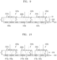
- FIG. 9 is a view illustrating an image sensor according to another exemplary embodiment.
- FIG. 9 a repeated explanation of the same elements or operations as those in FIGS. 1 through 8 will not be given.
- the image sensor may include a substrate 210 , a plurality of thin lenses 220 a , 220 b , and 220 c that are formed on a first surface S 1 of the substrate 210 and concentrate pieces of light that are incident on the first surface S 1 , and a plurality of light-sensing cells 230 a , 230 b , and 230 c that are formed on a second surface S 2 facing the first surface S 1 of the substrate 210 and generate electrical signals upon sensing light that has transmitted through the plurality of thin lenses 220 a , 220 b , and 220 c.
- the substrate 210 may include a transparent material.
- the term “transparent material” denotes a material having a high light transmittance.
- the substrate 210 may include at least one from among Si 3 N 4 , SiO 2 , and a polymer such as PMMA or PDMS.
- FIG. 10 is a view illustrating an example of the substrate 210 including a plurality of sub-substrates 210 a , 210 b , and 210 c , according to an exemplary embodiment.
- the sub-substrates 210 a , 210 b , and 210 c may be formed in correspondence to a respective thin lens of the plurality of thin lenses 220 a , 220 b , and 220 c and a respective light-sensing cell of the plurality of light-sensing cells 230 a , 230 b , and 230 c .
- a first thin-lens 220 a and a first light-sensing cell 230 a may be formed on a first and second surface of a first sub-substrate 210 a , respectively.
- a second thin-lens 220 b and a second light-sensing cell 230 b may be formed on a first and second surface of a second sub-substrate 210 b , respectively.
- a third thin-lens 220 c and a third light-sensing cell 230 c may be formed on a first and second surface of a third sub-substrate 210 c , respectively.
- the thin lenses 220 a , 220 b , and 220 c may include a plurality of scatterers 222 a , 222 b , and 222 c . At least two from among the thin lenses 220 a , 220 b , and 220 c may be configured to concentrate pieces of the incident light on the light-sensing cells 230 a , 230 b , and 230 c to have different focal lengths.
- the first thin-lens 220 a may concentrate pieces of the incident light to have a first focal length f 1 in a direction toward the first light-sensing cell 230 a .
- the second thin-lens 220 b may concentrate pieces of the incident light to have a second focal length f 2 in a direction toward the second light-sensing cell 230 b .
- the third thin-lens 220 c may concentrate pieces of the incident light to have a third focal length f 3 in a direction toward the third light-sensing cell 230 c . This is provided herein as an example only, and exemplary embodiments are not limited thereto.
- the first through third thin lenses 220 a , 220 b , and 220 c do not necessarily have to concentrate pieces of incident light to have focal lengths that are all different from one another, and two from among the first through third thin lenses 220 a , 220 b , and 220 c may concentrate pieces of incident light to have substantially the same focal length.
- the scatterers 222 a , 222 b , and 222 c included in the thin lenses 220 a , 220 b , and 220 c may have pillar structures.
- the scatterers 222 a , 222 b , and 222 c may have a shape of a cross-section of the pillar structure that may be from among a circle, an oval, a rectangle, and a square.
- the scatterers 222 a , 222 b , and 222 c may have a polygonal prism shape or a pillar structure with a cross-section having an “L”-like shape. Shapes of the scatterers 222 a , 222 b , and 222 c may not have symmetricity in a direction.
- a cross-section of the scatterers 222 a , 222 b , and 222 c may have a shape that is not symmetrical in a horizontal direction as, for example, an oval shape.
- the shapes of the scatterers 222 a , 222 b , and 222 c may be asymmetric with respect to the height.
- Shapes of the scatterers 222 a , 222 b , and 222 c may vary depending on focal lengths of the thin lenses 220 a , 220 b , and 220 c .
- scatterers 222 a included in the first thin-lens 220 a may have a shape appropriate to concentrate pieces of light to have a first focal length f 1 .
- a cross-sectional shape of the scatterers 222 a and a ratio between a width and a height of the scatterers 122 a may change.
- scatterers 222 b included in the second thin-lens 220 b may have a shape appropriate to concentrate pieces of light to have a second focal length f 2 .
- scatterers 222 c included in the third thin-lens 220 c may have a shape appropriate to concentrate pieces of light to have a third focal length f 3 . At least two from among the first through third focal lengths f 1 , f 2 , and f 3 may be different from each other. Also, interval distances among the scatterers 222 a , 222 b , and 222 c and heights of the scatterers 222 a , 222 b , and 222 c may differ according to focal lengths of the thin lenses 220 a , 220 b , and 220 c.
- images that are defocused to different degrees may be formed on the light-sensing cells 230 a , 230 b , and 230 c .
- Defocusing degrees of the images formed on the light-sensing cells 230 a , 230 b , and 230 c may differ according to the focal lengths of the thin lenses 220 a , 220 b , and 220 c and distances between an object and the thin lenses 220 a , 220 b , and 220 c .
- FIG. 11 is a view illustrating an image sensor according to an exemplary embodiment.
- the image sensor may further include a depth map calculator 250 that is configured to calculate depth map information of an image corresponding to incident light.
- the depth map calculator 250 may receive images measured by the light-sensing cells 230 a , 230 b , and 230 c .
- the depth map calculator 250 may recognize a relative blur degree for each position of the images measured by one from among the light-sensing cells 230 a , 230 b , and 230 c .
- the depth map calculator 250 may calculate a defocusing degree for each position of the images measured by one from among the light-sensing cells 230 a , 230 b , and 230 c.
- the depth map calculator 250 may calculate depth map information of an image corresponding to the incident light from the defocusing degree measured by each of the light-sensing cells 230 a , 230 b , and 230 c and the focal length of each of the thin lenses 220 a , 220 b , and 220 c .
- the depth map calculator 250 may calculate a distance from each of a plurality of points on each of objects or a surface of an object included in the image to each of the thin lenses 220 a , 220 b , and 220 c .
- the image sensor may obtain a 3-dimensional image of the object.
- the thin lenses 220 a , 220 b , and 220 c may each concentrate pieces of light having a predetermined wavelength component.
- the thin lenses 220 a , 220 b , and 220 c may function as an optical device with respect to a predetermined wavelength band of incident light. Shapes, a shape of arrangement, interval distances, and heights of the scatterers 222 a , 222 b , and 222 c included in the thin lenses 220 a , 220 b , and 220 c may be determined according to wavelength selectivity of the thin lenses 220 a , 220 b , and 220 c.
- all the thin lenses 220 a , 220 b , and 220 c may have substantially the same wavelength selectivity.
- the thin lenses 220 a , 220 b , and 220 c may all concentrate light of substantially the same wavelength component.
- shapes, a shape of arrangement, interval distances, and heights of the scatterers 222 a , 222 b , and 222 c included in the thin lenses 220 a , 220 b , and 220 c may be determined according to focal lengths of the thin lenses 220 a , 220 b , and 220 c . Heights and interval distances of the scatterers 222 a , 222 b , and 222 c may be smaller than a wavelength of light that is concentrated by the thin lenses 220 a , 220 b , and 220 c.
- FIG. 12 is a view illustrating an image sensor according to an exemplary embodiment.
- the image sensor may include a light filter layer 240 that filters wavelength components of light incident on each of the light-sensing cells 230 a , 230 b , and 230 c .
- the light filter layer 240 illustrated in FIG. 12 is prepared at a position where the light incident on the light-sensing cells 230 a , 230 b , and 230 c travels, exemplary embodiments are not limited thereto.
- the light filter layer 240 may be positioned between the thin lenses 220 a , 220 b , and 220 c and the light sensing layer 230 including the light-sensing cells 230 a , 230 b , and 230 c .
- the light filter layer 240 may allow a predetermined wavelength ⁇ 0 component among the incident light to transmit therethrough and may reflect or absorb the remaining wavelength components. Because the light filter layer 240 filters the wavelengths of the incident light, noise light of undesired wavelengths may be prevented from being incident on the light-sensing cells 230 a , 230 b , and 230 c . Also, quality of images obtained from the light-sensing cells 230 a , 230 b , and 230 c may improve.
- the thin lenses 220 a , 220 b , and 220 c may each concentrate pieces of light having different wavelengths to have different focal lengths.
- the first thin-lens 220 a may concentrate light having a first wavelength ⁇ 1 to have a first focal length f 1 .
- the scatterers 222 a included in the first thin-lens 220 a may have a shape of arrangement and interval distances appropriate to concentrate pieces of light having the first wavelength ⁇ 1 to have the first focal length f 1 .
- the second thin-lens 220 b may concentrate light having a second wavelength ⁇ 2 to have a second focal length f 2 .
- the scatterers 222 b included in the second thin-lens 220 b may have a shape of arrangement and interval distances appropriate to concentrate pieces of light having the second wavelength ⁇ 2 to have the second focal length f 2 .
- the third thin-lens 220 c may concentrate light having a third wavelength ⁇ 3 to have a third focal length f 3 .
- the scatterers 222 c included in the third thin-lens 220 c may have a shape of arrangement and interval distances appropriate to concentrate pieces of light having the third wavelength ⁇ 3 to have the third focal length f 3 .
- Heights and interval distances of the scatterers 222 a , 222 b , and 222 c included in the thin lenses 220 a , 220 b , and 220 c may vary according to wavelength selectivities of 220 a , 220 b , and 220 c , respectively.
- interval distances between the scatterers 222 a and heights of the scatterers 222 a in the first thin-lens 220 a may be smaller than the first wavelength ⁇ 1 .
- interval distances between the scatterers 222 b and heights of the scatterers 222 b in the second thin-lens 220 b may be smaller than the second wavelength ⁇ 2 .
- interval distances between the scatterers 222 c and heights of the scatterers 222 c in the third thin-lens 220 c may be smaller than the third wavelength ⁇ 3 .
- FIG. 13 is a view illustrating an image sensor according to an exemplary embodiment.
- the image sensor may include a light filter layer 240 configured to filter wavelength components of light incident on each of the light-sensing cells 230 a , 230 b , and 230 c .
- the light filter layer 240 may include a plurality of light filters 240 a , 240 b , and 240 c .
- the light filters 240 a , 240 b , and 240 c may be applied in correspondence to the light-sensing cells 230 a , 230 b , and 230 c .
- a first light filter 240 a may be configured to filter a wavelength of light incident on a first light-sensing cell 230 a .
- a second light filter 240 b may be configured to filter a wavelength of light incident on a second light-sensing cell 230 b .
- a third light filter 240 c may be configured to filter a wavelength of light incident on a third light-sensing cell 230 c.
- the first light filter 240 a may transmit a predetermined wavelength component among incident light according to a wavelength selectivity of the first thin-lens 220 a .
- the first light filter 240 a may allow light having a first wavelength ⁇ 1 to transmit therethrough and reflect or absorb light of the remaining wavelength components.
- the second light filter 240 b may allow light having a second wavelength ⁇ 2 to transmit therethrough and reflect or absorb light of the remaining wavelength components.
- the third light filter 240 c may allow light having a third wavelength ⁇ 3 to transmit therethrough and reflect or absorb light of the remaining wavelength components.
- the light filters 240 a , 240 b , and 240 c filter wavelengths of incident light, noise light of undesired wavelengths may be prevented from being incident on the light-sensing cells 230 a , 230 b , and 230 c . Also, quality of images obtained from the light-sensing cells 230 a , 230 b , and 230 c may improve. Further, the light-sensing cells 230 a , 230 b , and 230 c each generate images in different colors, and thus a multi-color image may be produced by synthesizing the images.
- FIG. 14 is a cross-sectional view illustrating an image sensor according to another exemplary embodiment.
- an image sensor 1000 includes a substrate 600 , a first thin lens 610 including a plurality of first scatterers 611 arranged on the substrate 600 and formed of a material having a higher refractive index than a refractive index of the substrate 600 , and configured to concentrate light having a first wavelength ⁇ 1 , and a plurality of light-sensing cells 510 sensing light that passed through the first thin lens 610 .
- the first thin lens 610 and the light-sensing cells 510 are spaced apart by a predetermined distance, and a housing 400 maintaining this distance may be further included.
- the predetermined distance may be set in consideration of a focal length f 0 of the first thin lens 610 .
- the housing 400 may fix both side portions of the substrate 600 on which the plurality of first scatterers 611 are formed and of a sensor substrate 500 including the plurality of light-sensing cells 510 .
- the image sensor 1000 may also include a second thin lens 620 including a plurality of second scatterers 621 formed on the substrate 600 and configured to concentrate light of a second wavelength ⁇ 2 that is different from the first wavelength ⁇ 1 , and a third thin lens 630 including a plurality of third scatterers 631 formed on the substrate 600 and configured to concentrate light having a third wavelength ⁇ 3 that is different from the first wavelength ⁇ 1 and the second wavelength ⁇ 2 .
- the first wavelength ⁇ 1 , the second wavelength ⁇ 2 , and the third wavelength ⁇ 3 respectively refer to central wavelengths of wavelength bands when the first through third thin lenses 610 , 620 , and 630 respectively concentrate light of the wavelength bands.
- Each of the first scatterers 611 , the second scatterers 621 , and the third scatterers 631 may be formed of the materials as described with reference to FIGS. 2 through 5 , and have a pillar shape having various cross-sectional shapes having shape dimensions of a sub-wavelength.
- the first scatterers 611 , the second scatterers 621 , and the third scatterers 631 may have an interval distance of a sub-wavelength, and have a shape distribution for concentrating light of a wavelength.
- the first scatterers 611 , the second scatterers 621 , and the third scatterers 631 may have different shape distributions to concentrate light having different wavelengths from each other.
- a ‘sub-wavelength’ refers to a wavelength that is less than a central wavelength of a wavelength band concentrated by a thin lens in which the scatterers are included.
- shape distribution collectively refers to a shape, size, arrangement rules, and positional distribution thereof or the like.
- shape distributions that are different from each other means that any one or any combination of shapes, sizes, arrangement rules, and positional distributions thereof is different from the other.
- Each of first scatterers 611 may have a smaller shape dimension than the first wavelength ⁇ 1
- each of the second scatterers 621 may have a smaller shape dimension than the second wavelength ⁇ 2
- each of the third scatterers 631 may have a smaller shape dimension than the third wavelength ⁇ 3
- a distance between the first scatterers 611 may be less than the first wavelength ⁇ 1
- a distance between the second scatterers 621 may be less than the second wavelength ⁇ 2
- a distance between the third scatterers 631 may be less than the third wavelength ⁇ 3 .
- the first scatterers 611 , the second scatterers 621 , and the third scatterers 631 may be formed of a material having a higher refractive index than a refractive index of the material of the substrate 600 . Accordingly, when concentrating incident light, it may be advantageous to implement a desired focal length and transmittance. A difference between the refractive indices of the first scatterers 611 , the second scatterers 621 , and the third scatterers 631 and a refractive index of the substrate 600 may be, for example, two or more.
- FIG. 15 is a cross-sectional view of a thin lens that is included in an image sensor according to another exemplary embodiment.
- a thin lens 710 includes a plurality of first scatterers 711 and a plurality of second scatterers 716 .
- the first scatterers 711 and the second scatterers 716 are arranged to form different layers from each other.
- a low-refractive index material layer 750 covering the plurality of first scatterers 711 arranged on a substrate 700 may be formed, and the plurality of second scatterers 716 may be formed on the low-refractive index material layer 750 .
- Each of the first scatterers 711 and the second scatterers 716 may have a shape dimension of a sub-wavelength.
- a shape distribution of the first scatterers 711 and that of the second scatterers 716 are illustrated as being identical for convenience of illustration, but are not limited thereto.
- a shape distribution of the first scatterers 711 and a shape distribution of the second scatterers 716 may be adequately set to concentrate light having a first wavelength ⁇ 1 , and such that a bandwidth of a concentration wavelength is implemented.
- a width of a concentration wavelength band may be increased.
- a width of a concentration wavelength band may be a width corresponding to, for example, a red wavelength band or a green wavelength band or a blue wavelength band.
- FIG. 16 is a graph illustrating a function of the thin lens of FIG. 15 that focuses light of a wavelength.
- a graph marked by a dotted line is with respect to an example of single-layer scatterers
- a graph marked by a solid line is with respect to the example of the thin lens 710 of FIG. 15 .
- Central wavelengths of the two graphs are identical as ⁇ 1 , but bandwidths thereof are different as A and B, respectively, and when the first scatterers 711 and the second scatterers 716 are arranged as two layers as in the embodiment of FIG. 15 , a bandwidth is A, which is wider.
- FIG. 17 is a cross-sectional view illustrating an image sensor according to another exemplary embodiment.
- an image sensor 2000 includes a plurality of light-sensing cells 510 and a first thin lens 710 , a second thin lens 720 , and a third thin lens 730 that are respectively arranged to face the light-sensing cells 510 .
- the first thin lens 710 includes a plurality of first scatterers 711 and a plurality of second scatterers 716 .
- the first scatterers 711 and the second scatterers 716 are respectively arranged to form different layers.
- a low-refractive index material layer 750 covering the plurality of first scatterers 711 arranged on the substrate 700 may be formed, and the plurality of second scatterers 716 may be formed on the low-refractive index material layer 750 .
- the second thin lens 720 includes a plurality of third scatterers 721 arranged on the substrate 700 and formed of a material having a higher refractive index than a refractive index of the substrate 700 and a plurality of fourth scatterers 726 arranged to form a different layer from the plurality of third scatterers 721 and spaced apart from the third scatterers 721 , and concentrates light having a second wavelength ⁇ 2 that is different from a first wavelength ⁇ 1 .
- the third thin lens 730 includes a plurality of fifth scatterers 731 arranged on the substrate 700 and formed of a material having a higher refractive index than a refractive index of the substrate 700 and a plurality of sixth scatterers 736 arranged to form a different layer from the plurality of fifth scatterers 731 and spaced apart from the fifth scatterers 731 , and concentrates light having a third wavelength ⁇ 3 that is different from the first wavelength ⁇ 1 and the second wavelength ⁇ 2 .
- Each of the scatterers included in the first through third thin lenses 710 , 720 , and 730 may have a shape dimension less than a wavelength concentrated by each lens, and may have a shape distribution that is appropriate for a concentration wavelength band and a focal length to be implemented by each lens.
- Each of the first scatterers 711 and the second scatterers 716 may have a smaller shape dimension than the first wavelength ⁇ 1 , and a distance between the first scatterers 711 and a distance between the second scatterers 716 may be less than the first wavelength ⁇ 1 .
- a shape dimension of each of the third scatterers 721 and the fourth scatterers 726 and a distance between the third scatterers 721 and a distance between the fourth scatterers 726 may be less than the second wavelength ⁇ 2 .
- a shape dimension of each of the fifth scatterers 731 and the sixth scatterers 736 and a distance between the fifth scatterers 731 and a distance between the sixth scatterers 736 may be less than the third wavelength ⁇ 3 .
- the first wavelength ⁇ 1 , the second wavelength ⁇ 2 , and the third wavelength ⁇ 3 may be respectively central wavelengths of a red wavelength band, a green wavelength band, and a blue wavelength band, and the first through third thin lenses 710 , 720 , and 730 may concentrate light of a red wavelength band, a green wavelength band, and a blue wavelength band. Accordingly, the image sensor 2000 may obtain color image information included in incident light.
- the image sensor 2000 may further include an optical filter filtering incident light such that pieces of light respectively having the first wavelength ⁇ 1 , the second wavelength ⁇ 2 , and the third wavelength ⁇ 3 are respectively incident on the first through third thin lenses 710 , 720 , and 730 .
- FIG. 18 is a cross-sectional view illustrating an image sensor according to another exemplary embodiment.
- an image sensor 3000 includes a plurality of light-sensing cells 510 and a first thin lens 760 , a second thin lens 770 , and a third thin lens 780 that are respectively arranged to face the plurality of light-sensing cells 510 .
- the image sensor 3000 according to the present embodiment is different from the image sensor 2000 of FIG. 17 in that the first thin lens 760 , the second thin lens 770 , and the third thin lens 780 respectively concentrate light of an identical wavelength band by different focal lengths.
- the first thin lens 760 includes a plurality of first scatterers 761 and a plurality of second scatterers 766 .
- the first scatterers 761 and the second scatterers 766 are respectively arranged to form different layers from each other.
- a low-refractive index material layer 750 covering the plurality of first scatterers 761 arranged on the substrate 700 may be formed, and the plurality of second scatterers 766 may be formed on the low-refractive index material layer 750 .
- the first scatterers 761 and the second scatterers 766 may have a shape distribution for concentrating light having a first wavelength ⁇ 1 by a focal length f 1 .
- the second thin lens 770 includes a plurality of third scatterers 771 arranged on the substrate 700 and formed of a material having a higher refractive index than a refractive index of the substrate 700 , and a plurality of fourth scatterers 776 arranged on the low-refractive index material layer 750 covering the plurality of third scatterers 771 , wherein the fourth scatterers 776 form a different layer from the third scatterers 771 .
- the third scatterers 771 and the fourth scatterers 776 may have a shape distribution for concentrating light having the first wavelength ⁇ 1 by a focal length f 2 .
- the third thin lens 780 includes a plurality of fifth scatterers 781 arranged on the substrate 700 and formed of a material having a higher refractive index than a refractive index of the substrate 700 , and a plurality of sixth scatterers 786 arranged on the low-refractive index material layer 750 covering the plurality of fifth scatterers 781 , wherein the sixth scatterers 786 form a different layer from the fifth scatterers 781 .
- the fifth scatterers 781 and the sixth scatterers 786 may have a shape distribution for concentrating light having the first wavelength ⁇ 1 by a focal length f 3 .
- the image sensor 3000 may further include a depth map calculator 900 configured to calculate a defocusing degree of light that is concentrated by different focal lengths by the first thin lens 760 , the second thin lens 770 , and the third thin lens 780 , and is incident on the plurality of light-sensing cells 510 , and calculate depth map information of an image represented by the incident light based on the calculated defocusing degree. Accordingly, the image sensor 3000 may obtain depth information of an image included in incident light.
- a depth map calculator 900 configured to calculate a defocusing degree of light that is concentrated by different focal lengths by the first thin lens 760 , the second thin lens 770 , and the third thin lens 780 , and is incident on the plurality of light-sensing cells 510 , and calculate depth map information of an image represented by the incident light based on the calculated defocusing degree. Accordingly, the image sensor 3000 may obtain depth information of an image included in incident light.
- FIG. 19 is a cross-sectional view illustrating an image sensor according to another exemplary embodiment.
- an image sensor 4000 includes a plurality of light-sensing cells 510 and first through ninth thin lenses 810 , 820 , 830 , 840 , 850 , 860 , 870 , 880 , and 890 arranged to face the light-sensing cells 510 .
- the first thin lens 810 , the second thin lens 820 , and the third thin lens 830 concentrate light having a first wavelength ⁇ 1 by different focal lengths f 1 , f 2 , and f 3 .
- the fourth thin lens 840 , the fifth thin lens 850 , and the sixth thin lens 860 concentrate light having a second wavelength ⁇ 2 by different focal lengths f 1 , f 2 , and f 3 .
- the seventh thin lens 870 , the eighth thin lens 880 , and the ninth thin lens 890 concentrate light having a third wavelength ⁇ 3 by different focal lengths f 1 , f 2 , and f 3 .
- the first through ninth thin lenses 810 through 890 include a plurality of first through ninth scatterers SC 1 through SC 9 each arranged in a double layer structure.
- the first through ninth scatterers SC 1 through SC 9 have a shape distribution that is suitable for a concentration wavelength and focal length to be implemented by the first through ninth thin lenses 810 through 890 .
- the first wavelength ⁇ 1 , the second wavelength ⁇ 2 , and the third wavelength ⁇ 3 may respectively be central wavelengths of a red wavelength band, a green wavelength band, and a blue wavelength band
- the first through third thin lenses 810 , 820 , and 830 may concentrate light of a red wavelength band
- the fourth through sixth lenses 840 , 850 , and 860 may concentrate light of a green wavelength band
- the seventh through ninth lenses 870 , 880 , and 890 may concentrate light of a blue wavelength band. Accordingly, the image sensor 4000 may obtain color image information included in incident light.
- the image sensor 4000 may further include a depth map calculator 900 configured to calculate a defocusing degree of light having the first wavelength ⁇ 1 , light having the second wavelength ⁇ 2 , and light having the third wavelength ⁇ 3 , which are concentrated by different focal lengths and are incident on the plurality of light-sensing cells 510 , and calculate depth map information of an image represented by incident light based on the calculated defocusing degree. Accordingly, the image sensor 4000 may obtain, for each color, depth information of an image included in incident light.
- the image sensor 4000 may obtain color information and depth information of an image included in incident light.
- an image sensor has been described with reference to FIGS. 1 through 19 .
- the image sensor may concentrate pieces of incident light by using a plurality of thin lenses.
- a size of the image sensor may be reduced.
- at least one from among a plurality of operation characteristics of the thin lenses may be controlled by changing at least one from among shapes, a shape of arrangement, interval distances, and sizes of the thin lenses. Therefore, the image sensor may be easily manufactured.
- a 3-dimensional image, a multi-color image, and depth map information of an object may be easily obtained from imaged generated from a plurality of light-sensing cells.
Landscapes
- Physics & Mathematics (AREA)
- General Physics & Mathematics (AREA)
- Optics & Photonics (AREA)
- Engineering & Computer Science (AREA)
- Multimedia (AREA)
- Signal Processing (AREA)
- Spectroscopy & Molecular Physics (AREA)
- Solid State Image Pick-Up Elements (AREA)
- Transforming Light Signals Into Electric Signals (AREA)
Abstract
Description
Claims (19)
Priority Applications (1)
| Application Number | Priority Date | Filing Date | Title |
|---|---|---|---|
| US16/284,087 US11089286B2 (en) | 2015-07-29 | 2019-02-25 | Image sensor |
Applications Claiming Priority (5)
| Application Number | Priority Date | Filing Date | Title |
|---|---|---|---|
| US201562198268P | 2015-07-29 | 2015-07-29 | |
| KR1020160044268A KR102496374B1 (en) | 2015-07-29 | 2016-04-11 | Image sensor |
| KR10-2016-0044268 | 2016-04-11 | ||
| US15/221,719 US10403668B2 (en) | 2015-07-29 | 2016-07-28 | Imaging apparatus and image sensor including the same |
| US16/284,087 US11089286B2 (en) | 2015-07-29 | 2019-02-25 | Image sensor |
Related Parent Applications (1)
| Application Number | Title | Priority Date | Filing Date |
|---|---|---|---|
| US15/221,719 Continuation-In-Part US10403668B2 (en) | 2015-07-29 | 2016-07-28 | Imaging apparatus and image sensor including the same |
Publications (2)
| Publication Number | Publication Date |
|---|---|
| US20190191144A1 US20190191144A1 (en) | 2019-06-20 |
| US11089286B2 true US11089286B2 (en) | 2021-08-10 |
Family
ID=66815278
Family Applications (1)
| Application Number | Title | Priority Date | Filing Date |
|---|---|---|---|
| US16/284,087 Active 2036-10-30 US11089286B2 (en) | 2015-07-29 | 2019-02-25 | Image sensor |
Country Status (1)
| Country | Link |
|---|---|
| US (1) | US11089286B2 (en) |
Cited By (2)
| Publication number | Priority date | Publication date | Assignee | Title |
|---|---|---|---|---|
| US20210103075A1 (en) * | 2019-10-08 | 2021-04-08 | Samsung Electronics Co., Ltd. | Meta lens and optical apparatus including the same |
| US11469265B2 (en) * | 2015-07-29 | 2022-10-11 | Samsung Electronics Co., Ltd. | Imaging apparatus and image sensor including the same |
Families Citing this family (14)
| Publication number | Priority date | Publication date | Assignee | Title |
|---|---|---|---|---|
| CN105487239B (en) * | 2015-11-13 | 2018-03-02 | 苏州苏大维格光电科技股份有限公司 | Directive property colored filter and bore hole 3D display device |
| US10930710B2 (en) * | 2017-05-04 | 2021-02-23 | Apple Inc. | Display with nanostructure angle-of-view adjustment structures |
| WO2019103762A2 (en) * | 2017-06-19 | 2019-05-31 | President And Fellows Of Harvard College | Topology optimized multi-layered meta-optics |
| CN119781177A (en) | 2017-08-31 | 2025-04-08 | 梅特兰兹股份有限公司 | Transmission-type metasurface lens integration |
| EP3799626A4 (en) | 2018-07-02 | 2022-03-30 | Metalenz, Inc. | METASURFACES TO ENSURE A REDUCTION OF LASER GRANULARITY |
| GB2576212B (en) * | 2018-08-10 | 2021-12-29 | X Fab Semiconductor Foundries Gmbh | Improvements in lens layers for semiconductor devices |
| KR102670423B1 (en) | 2018-10-22 | 2024-05-28 | 캘리포니아 인스티튜트 오브 테크놀로지 | Color and multi-spectral image sensors based on 3D engineered materials |
| EP4004608A4 (en) | 2019-07-26 | 2023-08-30 | Metalenz, Inc. | Aperture-metasurface and hybrid refractive-metasurface imaging systems |
| US11239276B2 (en) | 2019-10-18 | 2022-02-01 | California Institute Of Technology | CMOS color image sensors with metamaterial color splitting |
| US12320988B2 (en) | 2019-10-18 | 2025-06-03 | California Institute Of Technology | Broadband polarization splitting based on volumetric meta-optics |
| WO2021076154A1 (en) * | 2019-10-18 | 2021-04-22 | California Institute Of Technology | Cmos color image sensors with metamaterial color splitting |
| CN116368406B (en) * | 2020-10-12 | 2025-10-28 | 恩梯梯株式会社 | Optical element, imaging element, and imaging device |
| JP7828156B2 (en) | 2020-10-29 | 2026-03-11 | 三星電子株式会社 | Image sensor with color separation lens array and electronic device including the same |
| CA3246660A1 (en) | 2022-03-31 | 2025-02-03 | Metalenz, Inc. | Polarization sorting metasurface microlens array device |
Citations (34)
| Publication number | Priority date | Publication date | Assignee | Title |
|---|---|---|---|---|
| US5760834A (en) | 1992-09-30 | 1998-06-02 | Lsi Logic | Electronic camera with binary lens element array |
| US20080117519A1 (en) | 2006-11-17 | 2008-05-22 | Eastman Kodak Company | Light emitting device with microlens array |
| US20090097381A1 (en) | 2004-04-26 | 2009-04-16 | Yukiko Hamano | Optical pickup and optical information processing apparatus |
| US20090122178A1 (en) | 2007-11-12 | 2009-05-14 | Samsung Electronics Co., Ltd. | Camera module and electronic apparatus having the same |
| US20090219432A1 (en) | 2008-02-29 | 2009-09-03 | Palum Russell J | Sensor with multi-perspective image capture |
| JP2011099715A (en) | 2009-11-04 | 2011-05-19 | Panasonic Electric Works Co Ltd | Electromagnetic wave emission device and electromagnetic wave detector |
| US20110122308A1 (en) | 2009-11-20 | 2011-05-26 | Pelican Imaging Corporation | Capturing and processing of images using monolithic camera array with heterogeneous imagers |
| US20110228142A1 (en) | 2009-10-14 | 2011-09-22 | Fraunhofer-Gesellschaft Zur Foerderung Der Angewandten Forschung E.V. | Device, image processing device and method for optical imaging |
| US20110309237A1 (en) * | 2010-06-22 | 2011-12-22 | President And Fellows Of Harvard College | Light absorption and filtering properties of vertically oriented semiconductor nano wires |
| US20120091551A1 (en) | 2009-03-13 | 2012-04-19 | Norman Marenco | Method of manufacturing a multitude of micro-optoelectronic devices, and micro-optoelectronic device |
| US8169879B2 (en) | 2008-11-19 | 2012-05-01 | Kabushiki Kaisha Toshiba | Optical recording system to record information with light |
| US20120328240A1 (en) | 2010-02-12 | 2012-12-27 | The Regents Of The University Of California | Metamaterial-based optical lenses |
| US20130002253A1 (en) | 2011-05-02 | 2013-01-03 | Werner Douglas H | Isotropic metamaterial lens for magnetic imaging applications |
| US20130044187A1 (en) | 2011-08-18 | 2013-02-21 | Sick Ag | 3d camera and method of monitoring a spatial zone |
| US20130293760A1 (en) | 2012-05-01 | 2013-11-07 | Pelican Imaging Corporation | Camera modules patterned with pi filter groups |
| US20130321581A1 (en) | 2012-06-01 | 2013-12-05 | Ostendo Technologies, Inc. | Spatio-Temporal Light Field Cameras |
| US20140267890A1 (en) | 2013-03-13 | 2014-09-18 | Pelican Imaging Corporation | Systems and methods for controlling aliasing in images captured by an array camera for use in super-resolution processing |
| US20140267243A1 (en) | 2013-03-13 | 2014-09-18 | Pelican Imaging Corporation | Systems and Methods for Synthesizing Images from Image Data Captured by an Array Camera Using Restricted Depth of Field Depth Maps in which Depth Estimation Precision Varies |
| US20140277433A1 (en) | 2013-03-15 | 2014-09-18 | Johnson & Johnson Vision Care, Inc. | Ophthalmic devices incorporating metasurface elements |
| US20140263982A1 (en) | 2013-03-15 | 2014-09-18 | Raytheon Company | Sensor including dielectric metamaterial microarray |
| US20140307059A1 (en) | 2013-03-15 | 2014-10-16 | Sionyx, Inc. | Three dimensional imaging utilizing stacked imager devices and associated methods |
| US20140354855A1 (en) | 2008-05-20 | 2014-12-04 | Pelican Imaging Corporation | Systems and Methods for Synthesizing Higher Resolution Images Using Images Captured by Camera Arrays |
| US20150061066A1 (en) | 2012-11-08 | 2015-03-05 | Olympus Corporation | Imaging apparatus |
| US20150130973A1 (en) | 2012-05-16 | 2015-05-14 | Sony Corporation | Image-pickup optical system and image pickup apparatus |
| US20150373261A1 (en) | 2014-06-18 | 2015-12-24 | Pelican Imaging Corporation | Array Cameras and Array Camera Modules including Spectral Filters Disposed Outside of a Constituent Image Sensor |
| US20160198143A1 (en) | 2013-05-31 | 2016-07-07 | Nikon Corporation | Image sensor, imaging apparatus, and image processing device |
| US9406709B2 (en) * | 2010-06-22 | 2016-08-02 | President And Fellows Of Harvard College | Methods for fabricating and using nanowires |
| US20160299337A1 (en) | 2015-04-08 | 2016-10-13 | Samsung Electronics Co., Ltd. | Focusing device, and beam scanner and scope device including the focusing device |
| KR20160120653A (en) | 2015-04-08 | 2016-10-18 | 삼성전자주식회사 | Focusing device, beam scanner and scope device including the focusing device |
| KR20160125875A (en) | 2015-04-22 | 2016-11-01 | 삼성전자주식회사 | Imaging device and image sensor including the imaging device |
| US20170034500A1 (en) | 2015-07-29 | 2017-02-02 | Samsung Electronics Co., Ltd. | Imaging apparatus and image sensor including the same |
| US20180020209A1 (en) | 2014-12-22 | 2018-01-18 | Google Inc. | Integrated Camera System Having Two Dimensional Image Capture and Three Dimensional Time-of-Flight Capture With A Partitioned Field of View |
| US20180084238A1 (en) | 2016-09-21 | 2018-03-22 | Stmicroelectronics (Grenoble 2) Sas | Device having a 2d image sensor and depth sensor |
| US9946051B2 (en) | 2015-04-22 | 2018-04-17 | Samsung Electronics Co., Ltd. | Imaging apparatus and image sensor including the same |
-
2019
- 2019-02-25 US US16/284,087 patent/US11089286B2/en active Active
Patent Citations (36)
| Publication number | Priority date | Publication date | Assignee | Title |
|---|---|---|---|---|
| US5760834A (en) | 1992-09-30 | 1998-06-02 | Lsi Logic | Electronic camera with binary lens element array |
| US20090097381A1 (en) | 2004-04-26 | 2009-04-16 | Yukiko Hamano | Optical pickup and optical information processing apparatus |
| US20080117519A1 (en) | 2006-11-17 | 2008-05-22 | Eastman Kodak Company | Light emitting device with microlens array |
| US20090122178A1 (en) | 2007-11-12 | 2009-05-14 | Samsung Electronics Co., Ltd. | Camera module and electronic apparatus having the same |
| US20090219432A1 (en) | 2008-02-29 | 2009-09-03 | Palum Russell J | Sensor with multi-perspective image capture |
| US20140354855A1 (en) | 2008-05-20 | 2014-12-04 | Pelican Imaging Corporation | Systems and Methods for Synthesizing Higher Resolution Images Using Images Captured by Camera Arrays |
| US8169879B2 (en) | 2008-11-19 | 2012-05-01 | Kabushiki Kaisha Toshiba | Optical recording system to record information with light |
| US20120091551A1 (en) | 2009-03-13 | 2012-04-19 | Norman Marenco | Method of manufacturing a multitude of micro-optoelectronic devices, and micro-optoelectronic device |
| US20110228142A1 (en) | 2009-10-14 | 2011-09-22 | Fraunhofer-Gesellschaft Zur Foerderung Der Angewandten Forschung E.V. | Device, image processing device and method for optical imaging |
| JP2011099715A (en) | 2009-11-04 | 2011-05-19 | Panasonic Electric Works Co Ltd | Electromagnetic wave emission device and electromagnetic wave detector |
| US20130308197A1 (en) | 2009-11-20 | 2013-11-21 | Pelican Imaging Corporation | Capturing and Processing of Images Using Monolithic Camera Array with Heterogeneous Imagers |
| US20110122308A1 (en) | 2009-11-20 | 2011-05-26 | Pelican Imaging Corporation | Capturing and processing of images using monolithic camera array with heterogeneous imagers |
| US20120328240A1 (en) | 2010-02-12 | 2012-12-27 | The Regents Of The University Of California | Metamaterial-based optical lenses |
| US9406709B2 (en) * | 2010-06-22 | 2016-08-02 | President And Fellows Of Harvard College | Methods for fabricating and using nanowires |
| US20110309237A1 (en) * | 2010-06-22 | 2011-12-22 | President And Fellows Of Harvard College | Light absorption and filtering properties of vertically oriented semiconductor nano wires |
| US20130002253A1 (en) | 2011-05-02 | 2013-01-03 | Werner Douglas H | Isotropic metamaterial lens for magnetic imaging applications |
| US20130044187A1 (en) | 2011-08-18 | 2013-02-21 | Sick Ag | 3d camera and method of monitoring a spatial zone |
| US20130293760A1 (en) | 2012-05-01 | 2013-11-07 | Pelican Imaging Corporation | Camera modules patterned with pi filter groups |
| US20150130973A1 (en) | 2012-05-16 | 2015-05-14 | Sony Corporation | Image-pickup optical system and image pickup apparatus |
| US20130321581A1 (en) | 2012-06-01 | 2013-12-05 | Ostendo Technologies, Inc. | Spatio-Temporal Light Field Cameras |
| US20150061066A1 (en) | 2012-11-08 | 2015-03-05 | Olympus Corporation | Imaging apparatus |
| US20140267890A1 (en) | 2013-03-13 | 2014-09-18 | Pelican Imaging Corporation | Systems and methods for controlling aliasing in images captured by an array camera for use in super-resolution processing |
| US20140267243A1 (en) | 2013-03-13 | 2014-09-18 | Pelican Imaging Corporation | Systems and Methods for Synthesizing Images from Image Data Captured by an Array Camera Using Restricted Depth of Field Depth Maps in which Depth Estimation Precision Varies |
| US20140277433A1 (en) | 2013-03-15 | 2014-09-18 | Johnson & Johnson Vision Care, Inc. | Ophthalmic devices incorporating metasurface elements |
| US20140307059A1 (en) | 2013-03-15 | 2014-10-16 | Sionyx, Inc. | Three dimensional imaging utilizing stacked imager devices and associated methods |
| US20140263982A1 (en) | 2013-03-15 | 2014-09-18 | Raytheon Company | Sensor including dielectric metamaterial microarray |
| US20160198143A1 (en) | 2013-05-31 | 2016-07-07 | Nikon Corporation | Image sensor, imaging apparatus, and image processing device |
| US20150373261A1 (en) | 2014-06-18 | 2015-12-24 | Pelican Imaging Corporation | Array Cameras and Array Camera Modules including Spectral Filters Disposed Outside of a Constituent Image Sensor |
| US20180020209A1 (en) | 2014-12-22 | 2018-01-18 | Google Inc. | Integrated Camera System Having Two Dimensional Image Capture and Three Dimensional Time-of-Flight Capture With A Partitioned Field of View |
| US20160299337A1 (en) | 2015-04-08 | 2016-10-13 | Samsung Electronics Co., Ltd. | Focusing device, and beam scanner and scope device including the focusing device |
| KR20160120653A (en) | 2015-04-08 | 2016-10-18 | 삼성전자주식회사 | Focusing device, beam scanner and scope device including the focusing device |
| US9995930B2 (en) | 2015-04-08 | 2018-06-12 | Samsung Electronics Co., Ltd. | Focusing device comprising a plurality of scatterers and beam scanner and scope device |
| KR20160125875A (en) | 2015-04-22 | 2016-11-01 | 삼성전자주식회사 | Imaging device and image sensor including the imaging device |
| US9946051B2 (en) | 2015-04-22 | 2018-04-17 | Samsung Electronics Co., Ltd. | Imaging apparatus and image sensor including the same |
| US20170034500A1 (en) | 2015-07-29 | 2017-02-02 | Samsung Electronics Co., Ltd. | Imaging apparatus and image sensor including the same |
| US20180084238A1 (en) | 2016-09-21 | 2018-03-22 | Stmicroelectronics (Grenoble 2) Sas | Device having a 2d image sensor and depth sensor |
Non-Patent Citations (1)
| Title |
|---|
| Arbabi et al., "Subwavelength-thick lenses with high numerical apertures and large efficiency based on high-contrast transmitarrays", May 7, 2015, 6 pages total, Nature Communications. |
Cited By (3)
| Publication number | Priority date | Publication date | Assignee | Title |
|---|---|---|---|---|
| US11469265B2 (en) * | 2015-07-29 | 2022-10-11 | Samsung Electronics Co., Ltd. | Imaging apparatus and image sensor including the same |
| US20210103075A1 (en) * | 2019-10-08 | 2021-04-08 | Samsung Electronics Co., Ltd. | Meta lens and optical apparatus including the same |
| US11747524B2 (en) * | 2019-10-08 | 2023-09-05 | Samsung Electronics Co., Ltd. | Meta lens and optical apparatus including the same |
Also Published As
| Publication number | Publication date |
|---|---|
| US20190191144A1 (en) | 2019-06-20 |
Similar Documents
| Publication | Publication Date | Title |
|---|---|---|
| US11089286B2 (en) | Image sensor | |
| US11037976B2 (en) | Imaging apparatus and image sensor including the same | |
| US11211418B2 (en) | Imaging apparatus and image sensor including the same | |
| US11428929B2 (en) | Focusing device comprising a plurality of scatterers and beam scanner and scope device | |
| US12294013B2 (en) | Image-capture element and image capture device | |
| US20210318516A1 (en) | Optical system | |
| US11698510B2 (en) | Imaging apparatus and image sensor including the same | |
| US20220046175A1 (en) | Zoomable image sensor and image sensing method | |
| KR102601597B1 (en) | Focusing device, beam scanner and scope device including the focusing device | |
| KR102659161B1 (en) | Imaging device and image sensor including the imaging device | |
| CN101971636A (en) | camera device | |
| US20200166744A1 (en) | Focusing device comprising a plurality of scatterers and beam scanner and scope device | |
| WO2021070305A1 (en) | Spectral element array, imaging element, and imaging device | |
| US20110090317A1 (en) | Stereovision system and method for calcualting distance between object and diffractive optical element | |
| TWI772902B (en) | Image sensor and image apparatus | |
| US11994671B2 (en) | Focusing device comprising a plurality of scatterers and beam scanner and scope device | |
| KR20170015108A (en) | Image sensor | |
| WO2025021557A1 (en) | An integrated device, an imaging system, and a method for wavelength dependent detection of light |
Legal Events
| Date | Code | Title | Description |
|---|---|---|---|
| AS | Assignment |
Owner name: CALIFORNIA INSTITUTE OF TECHNOLOGY, CALIFORNIA Free format text: ASSIGNMENT OF ASSIGNORS INTEREST;ASSIGNORS:ARBABI, AMIR;HAN, SEUNGHOON;FARAON, ANDREI;SIGNING DATES FROM 20190211 TO 20190212;REEL/FRAME:048424/0001 Owner name: SAMSUNG ELECTRONICS CO., LTD., KOREA, REPUBLIC OF Free format text: ASSIGNMENT OF ASSIGNORS INTEREST;ASSIGNORS:ARBABI, AMIR;HAN, SEUNGHOON;FARAON, ANDREI;SIGNING DATES FROM 20190211 TO 20190212;REEL/FRAME:048424/0001 |
|
| FEPP | Fee payment procedure |
Free format text: ENTITY STATUS SET TO UNDISCOUNTED (ORIGINAL EVENT CODE: BIG.); ENTITY STATUS OF PATENT OWNER: LARGE ENTITY |
|
| STPP | Information on status: patent application and granting procedure in general |
Free format text: DOCKETED NEW CASE - READY FOR EXAMINATION |
|
| STPP | Information on status: patent application and granting procedure in general |
Free format text: NON FINAL ACTION MAILED |
|
| STPP | Information on status: patent application and granting procedure in general |
Free format text: RESPONSE TO NON-FINAL OFFICE ACTION ENTERED AND FORWARDED TO EXAMINER |
|
| STPP | Information on status: patent application and granting procedure in general |
Free format text: NOTICE OF ALLOWANCE MAILED -- APPLICATION RECEIVED IN OFFICE OF PUBLICATIONS |
|
| STPP | Information on status: patent application and granting procedure in general |
Free format text: AWAITING TC RESP., ISSUE FEE NOT PAID |
|
| STPP | Information on status: patent application and granting procedure in general |
Free format text: NOTICE OF ALLOWANCE MAILED -- APPLICATION RECEIVED IN OFFICE OF PUBLICATIONS |
|
| STPP | Information on status: patent application and granting procedure in general |
Free format text: PUBLICATIONS -- ISSUE FEE PAYMENT VERIFIED |
|
| STCF | Information on status: patent grant |
Free format text: PATENTED CASE |
|
| MAFP | Maintenance fee payment |
Free format text: PAYMENT OF MAINTENANCE FEE, 4TH YEAR, LARGE ENTITY (ORIGINAL EVENT CODE: M1551); ENTITY STATUS OF PATENT OWNER: LARGE ENTITY Year of fee payment: 4 |