WO2014069866A1 - 인쇄전자용 구리 페이스트 조성물 - Google Patents
인쇄전자용 구리 페이스트 조성물 Download PDFInfo
- Publication number
- WO2014069866A1 WO2014069866A1 PCT/KR2013/009664 KR2013009664W WO2014069866A1 WO 2014069866 A1 WO2014069866 A1 WO 2014069866A1 KR 2013009664 W KR2013009664 W KR 2013009664W WO 2014069866 A1 WO2014069866 A1 WO 2014069866A1
- Authority
- WO
- WIPO (PCT)
- Prior art keywords
- copper
- paste composition
- printed electronics
- nanoparticles
- weight
- Prior art date
- Legal status (The legal status is an assumption and is not a legal conclusion. Google has not performed a legal analysis and makes no representation as to the accuracy of the status listed.)
- Ceased
Links
Images
Classifications
-
- H—ELECTRICITY
- H01—ELECTRIC ELEMENTS
- H01B—CABLES; CONDUCTORS; INSULATORS; SELECTION OF MATERIALS FOR THEIR CONDUCTIVE, INSULATING OR DIELECTRIC PROPERTIES
- H01B1/00—Conductors or conductive bodies characterised by the conductive materials; Selection of materials as conductors
- H01B1/20—Conductive material dispersed in non-conductive organic material
- H01B1/22—Conductive material dispersed in non-conductive organic material the conductive material comprising metals or alloys
-
- C—CHEMISTRY; METALLURGY
- C09—DYES; PAINTS; POLISHES; NATURAL RESINS; ADHESIVES; COMPOSITIONS NOT OTHERWISE PROVIDED FOR; APPLICATIONS OF MATERIALS NOT OTHERWISE PROVIDED FOR
- C09D—COATING COMPOSITIONS, e.g. PAINTS, VARNISHES OR LACQUERS; FILLING PASTES; CHEMICAL PAINT OR INK REMOVERS; INKS; CORRECTING FLUIDS; WOODSTAINS; PASTES OR SOLIDS FOR COLOURING OR PRINTING; USE OF MATERIALS THEREFOR
- C09D11/00—Inks
- C09D11/52—Electrically conductive inks
-
- H—ELECTRICITY
- H05—ELECTRIC TECHNIQUES NOT OTHERWISE PROVIDED FOR
- H05K—PRINTED CIRCUITS; CASINGS OR CONSTRUCTIONAL DETAILS OF ELECTRIC APPARATUS; MANUFACTURE OF ASSEMBLAGES OF ELECTRICAL COMPONENTS
- H05K1/00—Printed circuits
- H05K1/02—Details
- H05K1/09—Use of materials for the conductive, e.g. metallic pattern
- H05K1/092—Dispersed materials, e.g. conductive pastes or inks
- H05K1/095—Dispersed materials, e.g. conductive pastes or inks for polymer thick films, i.e. having a permanent organic polymeric binder
-
- H—ELECTRICITY
- H05—ELECTRIC TECHNIQUES NOT OTHERWISE PROVIDED FOR
- H05K—PRINTED CIRCUITS; CASINGS OR CONSTRUCTIONAL DETAILS OF ELECTRIC APPARATUS; MANUFACTURE OF ASSEMBLAGES OF ELECTRICAL COMPONENTS
- H05K1/00—Printed circuits
- H05K1/02—Details
- H05K1/03—Use of materials for the substrate
- H05K1/0393—Flexible materials
-
- H—ELECTRICITY
- H05—ELECTRIC TECHNIQUES NOT OTHERWISE PROVIDED FOR
- H05K—PRINTED CIRCUITS; CASINGS OR CONSTRUCTIONAL DETAILS OF ELECTRIC APPARATUS; MANUFACTURE OF ASSEMBLAGES OF ELECTRICAL COMPONENTS
- H05K1/00—Printed circuits
- H05K1/02—Details
- H05K1/09—Use of materials for the conductive, e.g. metallic pattern
- H05K1/092—Dispersed materials, e.g. conductive pastes or inks
- H05K1/097—Inks comprising nanoparticles and specially adapted for being sintered at low temperature
-
- H—ELECTRICITY
- H05—ELECTRIC TECHNIQUES NOT OTHERWISE PROVIDED FOR
- H05K—PRINTED CIRCUITS; CASINGS OR CONSTRUCTIONAL DETAILS OF ELECTRIC APPARATUS; MANUFACTURE OF ASSEMBLAGES OF ELECTRICAL COMPONENTS
- H05K2201/00—Indexing scheme relating to printed circuits covered by H05K1/00
- H05K2201/02—Fillers; Particles; Fibers; Reinforcement materials
- H05K2201/0203—Fillers and particles
- H05K2201/0206—Materials
- H05K2201/0218—Composite particles, i.e. first metal coated with second metal
-
- H—ELECTRICITY
- H05—ELECTRIC TECHNIQUES NOT OTHERWISE PROVIDED FOR
- H05K—PRINTED CIRCUITS; CASINGS OR CONSTRUCTIONAL DETAILS OF ELECTRIC APPARATUS; MANUFACTURE OF ASSEMBLAGES OF ELECTRICAL COMPONENTS
- H05K2201/00—Indexing scheme relating to printed circuits covered by H05K1/00
- H05K2201/02—Fillers; Particles; Fibers; Reinforcement materials
- H05K2201/0203—Fillers and particles
- H05K2201/0206—Materials
- H05K2201/0224—Conductive particles having an insulating coating
Definitions
- the present invention relates to a copper paste composition for printed electronics, and more particularly, to a copper paste composition for printed electronics including copper nanoparticles whose oxidation is suppressed and excellent in electrical conductivity, adhesion to a substrate, and printability.
- Printed electronics technology is a technology that manufactures a variety of electronic devices, components or modules using a direct printing process of various functional ink materials capable of solution processing.
- RFID tags, lighting, displays, solar cells It can be applied to almost all areas where semiconductors, devices, circuits, and the like are used.
- conductive ink materials are mainly used for electrodes and wiring of various electronic devices, and the most important physical property necessary for the conductive lines formed at this time is conductivity, and the next important requirements are low process temperature, Low production cost, ink stability, and the like.
- the conductive ink materials which are mainly used or actively studied at present include conductive polymer solutions, solutions in which metal nanoparticles are dispersed, carbon nanotube (CNT) dispersion solutions, and composite materials thereof.
- Metal nanoparticles which are currently being actively studied, have high conductivity, but require a relatively high firing temperature (> 150 ° C.) in order to remove the dispersant used to disperse them.
- a composition composed mainly of spherical micro ( ⁇ m) -sized silver (Ag) has been used as a paste, and the paste made of silver has been widely applied because it is easy to manufacture and has excellent stability and stable after printing. Due to the high price and high price, it has a negative effect on the cost of the produced product, and the spherical micro silver particles are difficult to realize high electrical conductivity at low temperature.
- an object of the present invention is to provide a copper paste composition for printed electronics that can suppress the oxidation of copper to exhibit excellent electrical conductivity, adhesion and printability.
- Another object of the present invention is to provide a printed electronic method capable of exhibiting excellent electrical conductivity, adhesive strength and printability using the copper paste composition for printed electronics, and a printed electronic article manufactured by the method.
- the present invention to achieve the above object
- the present invention provides a printed electronic method comprising the step of performing drying and firing after printing the copper paste composition for printed electronics on a substrate.
- the present invention provides a printed electronic article manufactured by the printed electronic method.
- the copper paste composition for printed electronics according to the present invention can exhibit excellent conductivity and printability even at atmospheric pressure by using copper nanoparticles, copper-dissimilar metal nanoparticles or a mixture thereof, which are synthesized by wet synthesis and thinly coated with organic material on the surface.
- copper- dissimilar metal nanoparticles since the adhesion is excellent, it can be applied to various printed electronics instead of expensive silver particles.
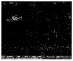
- FIG. 1 is a photograph showing copper nanoparticles synthesized in Synthesis Example 1.
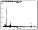
- Figure 2 is a graph showing the EDAX surface analysis of the copper nanoparticles synthesized in Synthesis Example 1.
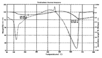
- Figure 3 is a graph showing the thermal analysis and organic content measurement results of the copper nanoparticles synthesized in Synthesis Example 1.
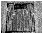
- Example 4 is a photograph showing the result of printing and baking the composition of Example 1 on a polyimide film.
- FIG. 5 is a photograph showing the results of evaluation of printability of the composition of Example 1.
- Copper particles of 1 ⁇ m or more that are generally sold on the market are difficult to achieve low resistance due to fusion between particles at low temperatures, and have a disadvantage of completely losing conductivity while oxidation occurs first when fused for a long time.
- commercially available copper particles do not have organic coatings on their surfaces and are easily oxidized.
- Copper nanoparticles coated with an organic material on the surface usable in the present invention may be a pure copper nanoparticles coated with an organic material, or copper- dissimilar metal nanoparticles may be coated with an organic material or a mixture thereof.
- the different metal in the above may be used without limitation as long as the metal is faster oxidation than copper commonly used in the art, preferably zinc or aluminum.
- pure copper nanoparticles do not show excellent results even if the polymer component is added to the adhesion between the polyimide and the polymer substrate.
- the pure copper nanoparticles differ in shrinkage from the substrate because the interface between particles increases and the shrinkage rate increases accordingly.
- the adhesion strength is not good, but the metal oxide is faster than the copper, in particular, in the case of forming copper-heterometallic nanoparticles in the form of solid solution of zinc or aluminum in the form of a solid solution, The adhesive strength is improved by reducing the difference in shrinkage.
- the content ratio of the copper and the dissimilar metal in the copper-dissimilar metal nanoparticles is preferably mixed with dissimilar metals in an amount of 1 to 30 parts by weight based on 100 parts by weight of copper.
- the nanoparticles are spherical, the average particle size is 50 to 1,000 nm, preferably 100 to 500 nm, the organic material is coated on the surface is characterized in that the oxidation is inhibited.
- the copper nanoparticles according to the present invention are inhibited from being oxidized by the organic film coated on the surface even when heat is applied at atmospheric pressure in which oxygen or more is present.
- the organic material may be an amine, fatty acid, aliphatic amine or mercapto, and the content of the surface organic material is preferably 0.1 to 10% by weight. In the case, it is possible to satisfy the desired electrical conductivity at the same time while preventing the oxidation of copper.
- the copper nanoparticles can be prepared using conventional methods, such as wet synthesis.
- the copper nanoparticles may be included in an amount of 40 to 90% by weight, and when added in an amount of less than 40% by weight, the binder content may be increased to achieve a desired conductivity.
- the viscoelastic properties for the sharp deterioration has a problem that the print performance is significantly reduced.
- the copper nanoparticles may be a mixture of 30 to 70 parts by weight of pure copper nanoparticles and 70 to 30 parts by weight of copper- dissimilar metal nanoparticles.
- a binder resin is included in order to give the paste composition an adhesive property and a rheological property for printing.
- Binder resins usable in the present invention include, but are not limited to, cellulose-based, for example methylcellulose, ethylcellulose, hydroxypropylcellulose, hydroxypropylmethylcellulose, cellulose acetate boot Rate, carboxymethyl cellulose, hydroxyethyl cellulose, epoxy resins, polyester resins and copolymers prepared by mixing at least one of them are preferred.
- the binder resin may be included in an amount of 1 to 30% by weight, and when added in an amount of less than 1% by weight, the viscosity of the paste may be increased, resulting in poor printability, and when the content exceeds 30% by weight, the viscosity of the paste may be increased.
- monomers or oligomers are used to increase the Viscosity property of the composition.
- one or more selected from the group consisting of acryl, urethane and epoxy may be used, for example urethane acrylate, polyfunctional acrylate, polyester acrylate urethane, etc., molecular weight of 10,000 It is preferable that it is the following.
- the monomer or oligomer may be included in an amount of 1 to 20% by weight, the elastic property may be excessively increased by the binder when added in less than 1% by weight, the fluidity may be excessively increased when it exceeds 20% by weight have.
- the curing agent may be added by adding a curing agent that can be cured by thermal baking.
- dimethylaminopropyl methacrylamide, isocyanate, phthalic anhydride and the like can be used as the curing agent usable in the present invention.
- the curing agent may be included in 0.1 to 3% by weight, it is difficult to secure the adhesive strength when it is added to less than 0.1% by weight, it is difficult to secure the adhesive strength, if more than 3% by weight rather than the adhesive strength due to the unreacted curing agent Can be dropped.
- a solvent is used to control the viscosity of the paste and to enhance the dispersion of the nanoparticles.
- Solvents usable in the present invention include diethylene glycol, triethylene glycol, tetraethylene glycol, diethylene glycol monomethyl ether, diethylene glycol monomethyl ether acetate, diethylene glycol monobutyl ether, diethylene glycol monobutyl ether acetate, Diethylene glycol monoethyl ether, diethylene glycol monoethyl ether acetate, dipropylene glycol monomethyl ether, dipropylene glycol monomethyl ether acetate, methyl pyrrolidone, terpinol, and the like can be used. It may be included as.
- the copper paste composition for printed electronics of the present invention may further include additives commonly used in the art, for example, antioxidants, pH adjusting agents, and the like, in addition to the above components.
- the present invention also provides a printed electronic method comprising the step of performing drying and firing after printing the copper paste composition for printed electronics on a substrate and a printed electronic article prepared according to the method.
- the printing may include screen printing, gravure off-set printing, and gravure direct.
- the substrate to be printed may be applied to a variety of known substrates, for example, may be printed on a flexible circuit board, a glass substrate.
- the substrate is a flexible circuit board, in particular, a polyimide (PI) film.
- the paste composition of the present invention is optimized to be suitable for each printing process, and when the screen printing method is applied to a polyimide (PI) film, the paste composition of the present invention has a viscosity range of 10,000 to 50,000 centipoise (cps). It is preferable to have.
- PI polyimide
- the copper paste composition of the present invention may be calcined according to the calcining method commonly used in the art after performing the printing process as described above, preferably nitrogen, oxygen or argon hot air alone, MIR (Middle infra red) Lamps, or hot air and MIR lamps can be used at the same time to dry and fire.
- nitrogen, oxygen or argon hot air alone, MIR (Middle infra red) Lamps, or hot air and MIR lamps can be used at the same time to dry and fire.
- composition according to the present invention is preferably dried or fired while supplying hot nitrogen or oxygen at 220 ° C. or lower, preferably 150 to 200 ° C., or dried and fired with a MIR lamp at 150 to 200 ° C.
- the composition according to the present invention can suppress oxidation at atmospheric pressure as much as possible by using copper nanoparticles coated with an organic material on the surface, as well as excellent electrical conductivity, adhesion and Because of its excellent printability, it can be applied to various printed electronic fields (for example, RFID tags, lighting, displays, solar cells, batteries, semiconductors, electronic devices, circuits, etc.) instead of expensive silver particles.
- the present invention can be preferably applied in the manufacture of flexible printed circuit boards.
- the dark red powder was recovered by centrifugation and precipitation, and washed and recovered several times with methanol, and then stored at atmospheric pressure.
- Copper-zinc nanoparticles were synthesized in the same manner as in Synthesis Example 1, except that 27 g of copper precursor CuCl 2 and 3 g of zinc precursor were used instead of 30 g of copper precursor CuCl 2 as the metal precursor.
- Copper-aluminum nanoparticles were synthesized in the same manner as in Synthesis Example 1, except that 27 g of copper precursor CuCl 2 and 3 g of aluminum precursor were used instead of 30 g of copper precursor CuCl 2 as the metal precursor.
- a paste composition was prepared in the same manner as in Example 1, except that 30 g of the copper-zinc nanoparticles prepared in Synthesis Example 2 was used instead of 30 g of the copper nanoparticles prepared in Synthesis Example 1.
- Example 1 except that 15 g of copper nanoparticles prepared in Synthesis Example 1 and 15 g of copper-zinc nanoparticles prepared in Synthesis Example 2 were used instead of 30 g of the copper nanoparticles prepared in Synthesis Example 1. In the same manner as in the paste composition was prepared.
- a paste composition was prepared in the same manner as in Example 1, except that a polyfunctional urethane acrylate oligomolecule having a molecular weight of 2,000 or more was used instead of an acrylic monomer.
- a paste composition was prepared in the same manner as in Example 1, except that a bisphenol-based epoxy oligomo having a molecular weight of 500 or more was used instead of the acrylic monomer.
- a paste composition was prepared in the same manner as in Example 1, except that 8 g of ethyl cellulose polymer and 2 g of epoxy resin were used instead of 10 g of ethyl cellulose polymer.
- a paste composition was prepared in the same manner as in Example 1, except that 8 g of ethyl cellulose polymer and 2 g of epoxy resin were used instead of 10 g of ethyl cellulose polymer, and a urethane based monomer was used instead of an acrylic monomer.
- a paste composition was prepared in the same manner as in Example 1, except that 8 g of ethyl cellulose polymer and 2 g of epoxy resin were used instead of 10 g of ethyl cellulose polymer, and an epoxy monomer was used instead of an acrylic monomer.
- a paste composition was prepared in the same manner as in Example 1, except that 30 g of copper particles purchased from Aldrich Inc. was used instead of 30 g of copper nanoparticles prepared in Synthesis Example 1.
- each composition was printed on a polyimide film through a 290 mesh screen net having a pattern formed thereon, and the formed coating film was dried at 50 ° C. After calcining with hot air at 200 ° C. for 3 minutes (FIG. 4), the conductivity was measured by directly measuring the printed pattern with a multi tester, and the printed pattern was evaluated for adhesive strength by the method of ASTM D3359. Table 1 shows.
- Example 1 Conductivity (line resistance 100 ⁇ m / 1 cm) Adhesion (PI Substrate ASTM D3359) Printability (with / without 50 ⁇ m single wire)
- Example 1 2.5 50 o
- Example 2 7.8 95 o
- Example 3 3.4 90 o
- Example 4 30.2 95 o
- Example 5 3.9 50 o
- Example 6 10.5 95 o
- Example 7 3.1 50 o
- Example 8 3.9 90 o
- Example 9 11.8 50 o
- Example 10 4.8 30 o
- Example 11 20.4 95 o
- Example 12 3.8 50 o
- Example 13 4.9 90 o
- Example 14 20.8 90 o Comparative Example 1 x 5 x
- the copper paste composition for printed electronics according to the present invention may exhibit excellent conductivity and printability even at atmospheric pressure by using copper nanoparticles, copper-dissimilar metal nanoparticles, or a mixture thereof, which are synthesized by wet synthesis and thinly coated with organic material on the surface.
- copper- dissimilar metal nanoparticles since the adhesion is excellent, it can be applied to various printed electronics instead of expensive silver particles.
Landscapes
- Chemical & Material Sciences (AREA)
- Dispersion Chemistry (AREA)
- Engineering & Computer Science (AREA)
- Microelectronics & Electronic Packaging (AREA)
- Physics & Mathematics (AREA)
- Spectroscopy & Molecular Physics (AREA)
- Life Sciences & Earth Sciences (AREA)
- Materials Engineering (AREA)
- Wood Science & Technology (AREA)
- Organic Chemistry (AREA)
- Conductive Materials (AREA)
Abstract
본 발명은 인쇄전자용 구리 페이스트 조성물에 관한 것으로, 더욱 상세하게는 산화가 억제된 구리 나노입자를 포함하여 전기전도도, 기판과의 접착력 및 인쇄성이 우수한 인쇄전자용 구리 페이스트 조성물에 관한 것이다. 구체적으로, 본 발명에 따른 인쇄전자용 구리 페이스트 조성물은 표면에 유기물이 얇게 코팅된 구리 나노입자 또는 구리-이종금속 나노입자를 사용함으로써 대기압에서도 우수한 전도도 및 인쇄성을 나타낼 수 있으며, 특히 구리-이종금속 나노입자를 사용할 경우, 접착력이 우수하므로, 고가의 은 입자를 대신하여 다양한 인쇄전자분야에 적용될 수 있다.
Description
본 발명은 인쇄전자용 구리 페이스트 조성물에 관한 것으로, 더욱 상세하게는 산화가 억제된 구리 나노입자를 포함하여 전기전도도, 기판과의 접착력 및 인쇄성이 우수한 인쇄전자용 구리 페이스트 조성물에 관한 것이다.
인쇄전자(printed electronics) 기술은 용액공정이 가능한 다양한 기능성 잉크소재(functional ink materials)를 직접 인쇄 공정을 이용하여 다양한 전자소자 및 부품 혹은 모듈을 제작하는 기술로, RFID 태그, 조명, 디스플레이, 태양전지, 전지(Battery) 등 반도체나 소자, 회로 등이 쓰이는 거의 모든 영역에 적용될 수 있다.
이러한 인쇄전자에 사용되는 잉크재료 중, 전도성 잉크재료는 각종 전자소자의 전극, 배선 등에 주로 사용되며 이때 형성되는 전도성 라인에 필요한 가장 중요한 물성은 바로 전도도이며, 다음으로 중요한 요구사항은 낮은 공정온도, 낮은 제조단가 및 잉크의 안정성 등을 들 수 있다. 현재 주로 사용되고 있거나 활발히 연구되고 있는 전도성 잉크재료로는 전도성 고분자 용액, 금속 나노입자가 분산된 용액, 탄소나노튜브(CNT) 분산 용액 및 이에 대한 복합체 재료를 들 수 있다.
현재 가장 활발히 연구되고 있는 금속 나노입자의 경우 높은 전도도를 보유하고 있으나, 이들을 분산시키기 위해 사용되는 분산제를 제거하기 위해서 비교적 높은 소성온도(>150℃)를 요구하며 제조 단가도 비싼 편이다.
최근까지 이러한 금속 잉크 페이스트로는 주로 구형의 마이크로(㎛) 크기의 은(Ag)으로 구성된 조성물이 쓰이고 있으며, 은으로 구성된 페이스트는 제조하기 쉽고 안정성이 뛰어나 인쇄 후에도 안정적인 장점이 있어 널리 응용이 되고 있지만 가격이 유동적이고 높기 때문에 생산제품의 단가에 안 좋은 영향을 미칠 수밖에 없으며, 구형의 마이크로 은 입자는 저온에서 높은 전기 전도도를 실현하기 어려운 단점이 있다.
이러한 문제를 해결하기 위하여, 각종 인쇄 공정에서 높은 가격의 은을 대체할 수 있으면서 기존공정에 그대로 적용이 가능한 구리(Cu)로 구성된 페이스트 조성물에 대한 관심이 높아지고 있지만, 구리는 대기압에서 산화가 잘 일어나는 단점이 있다.
이에, 상기와 같은 종래 비용이 많이 드는 은 조성물이나 구리 조성물의 산화 문제를 해결하고 하부기판과의 접착력이 향상된 구리 페이스트 조성물에 대한 개발이 절실한 실정이다.
상기와 같은 문제점을 해결하기 위해, 본 발명은 구리의 산화가 억제되어 우수한 전기 전도도, 접착력 및 인쇄성을 나타낼 수 있는 인쇄전자용 구리 페이스트 조성물을 제공하는 것을 목적으로 한다.
본 발명은 또한 상기 인쇄전자용 구리 페이스트 조성물을 이용하여 우수한 전기 전도도, 접착력 및 인쇄성을 나타낼 수 있는 인쇄전자방법 및 상기 방법에 의하여 제조된 인쇄전자물품을 제공하는 것을 목적으로 한다.
상기 목적을 달성하기 위해 본 발명은
a) 표면에 유기물이 코팅된 구리(Cu) 나노입자, 구리-이종금속 나노입자 또는 이들의 혼합물 40 내지 90 중량%;
b) 바인더 수지 1 내지 30 중량%;
c) 모노머 및 올리고머 1 내지 20 중량%;
d) 경화제 0.1 내지 3 중량%; 및
e) 잔량의 용매
를 포함하는 것을 특징으로 하는 인쇄전자용 구리 페이스트 조성물을 제공한다.
또한 본 발명은 인쇄전자용 구리 페이스트 조성물을 기재에 인쇄한 후 건조 및 소성을 수행하는 단계를 포함하는 것을 특징으로 하는 인쇄전자방법을 제공한다.
또한 본 발명은 상기 인쇄전자방법에 의하여 제조된 인쇄전자물품을 제공한다.
본 발명에 따른 인쇄전자용 구리 페이스트 조성물은 습식 합성법으로 합성되고 표면에 유기물이 얇게 코팅된 구리 나노입자, 구리-이종금속 나노입자 또는 이들의 혼합물을 사용함으로써 대기압에서도 우수한 전도도 및 인쇄성을 나타낼 수 있으며, 특히 구리-이종금속 나노입자를 사용할 경우, 접착력이 우수하므로, 고가의 은 입자를 대신하여 다양한 인쇄전자분야에 적용될 수 있다.
도 1은 합성예 1에서 합성된 구리 나노입자를 나타내는 사진이다.
도 2는 합성예 1에서 합성된 구리 나노입자의 EDAX 표면 분석 결과를 나타낸 그래프이다.
도 3은 합성예 1에서 합성된 구리 나노입자의 열분석 및 유기물 함량 측정 결과를 나타낸 그래프이다.
도 4는 실시예 1의 조성물을 폴리이미드 필름 위에 인쇄하고 소성한 결과를 나타낸 사진이다.
도 5는 실시예 1의 조성물의 인쇄성을 평가한 결과를 나타내는 사진이다.
본 발명에 따른 건조 및 소성이 동시에 가능한 인쇄용 구리 페이스트 조성물은 a) 표면에 유기물이 코팅된 구리(Cu) 나노입자, 구리-이종금속 나노입자 또는 이들의 혼합물 40 내지 90 중량%; b) 바인더 수지 1 내지 30 중량%; c) 모노머 및 올리고머 1 내지 20 중량%; d) 경화제 0.1 내지 3 중량%; 및 e) 잔량의 용매를 포함하는 것을 특징으로 한다.
이하 각 성분들에 대하여 설명한다.
a) 표면에 유기물이 코팅된 구리 나노입자
시중에서 일반적으로 판매되고 있는 1 ㎛ 이상의 구리 입자는 저온에서 입자간 융착이 일어나기 힘들어 저저항을 실현하기 힘들며, 장시간 가열하여 융착시킬 경우 산화가 먼저 일어나면서 전도도를 완전히 잃어버리는 단점이 있다. 또한 시중에서 판매되는 구리 입자의 경우 표면에 코팅된 유기물이 없어 쉽게 산화된다.
본 발명에서 사용가능한 표면에 유기물이 코팅된 구리 나노입자는 순수한 구리 나노입자에 유기물이 코팅되거나, 구리-이종금속 나노입자에 유기물이 코팅되거나 또는 이들의 혼합물일 수 있다. 상기에서 이종금속은 당분야에서 통상적으로 사용하는 구리보다 산화가 빠른 금속이라면 제한없이 사용될 수 있으나, 아연 또는 알루미늄인 것이 바람직하다. 또한 순수 구리 나노입자는 폴리이미드 및 폴리머 기판과의 접착력에 있어서 폴리머 성분을 첨가하더라도 뛰어난 결과를 보이지 못하며, 특히 소성시 입자끼리 융착하면서 입자간 경계면이 커지고 이에 따라 수축율이 커지기 때문에 기판과의 수축율 차이에 의해서 접착력이 좋지 못한 단점이 있으나, 구리보다 산화가 빠른 금속, 구체적인 일예로 아연이나 알루미늄을 고용체 형태로 구리-이종금속 나노입자를 형성할 경우 입자간 융착시 입자간 경계면의 크기를 조절하면서 기판과의 수축율 차이를 줄여 줌으로써 접착력이 좋아지는 장점이 있다. 상기 구리-이종금속 나노입자에서 상기 구리와 이종금속의 함량비율은 구리 100 중량부에 대하여 이종금속이 1 내지 30 중량부로 혼합되어 있는 것이 좋다.
본 발명에서 상기 나노입자는 구상이고, 평균입자크기가 50 내지 1,000 nm, 바람직하게는 100 내지 500 nm이며, 표면에 유기물이 코팅되어 산화가 억제된 것임을 특징으로 한다. 본 발명에 따른 구리 나노입자는 일정 이상의 산소가 존재하는 대기압 상에서 열이 가해지더라도 표면에 코팅된 유기막에 의해 산화가 억제된다.
상기 유기물은 아민, 지방산, 지방족아민 또는 머캅토류일 수 있으며, 표면 유기물의 함량은 0.1 내지 10 중량%인 것이 바람직하다. 상기 내인 경우 구리의 산화를 방지하면서 목적하는 전기전도도를 동시에 만족시킬 수 있다.
상기 구리 나노입자는 통상의 방법, 예를 들어, 습식 합성법을 이용하여 제조될 수 있다.
본 발명의 페이스트 조성물에서 상기 구리 나노입자는 40 내지 90 중량%로 포함될 수 있으며, 40 중량% 미만으로 첨가될 경우 상대적으로 바인더 함량이 높아져 원하는 전도도를 이룰 수 없으며, 90 중량%가 넘을 경우 인쇄를 위한 점탄성 특성이 급격히 나빠지면서 인쇄 성능이 현저히 떨어지는 문제가 있다. 바람직하기로 본 발명의 페이스트 조성물에서 상기 구리 나노입자는 순수한 구리 나노입자 30-70 중량부와 구리-이종금속 나노입자 70-30 중량부가 혼합되어 있는 것이 좋다.
b) 바인더 수지
본 발명에서는 페이스트 조성물에 접착력 및 인쇄를 위한 레올로지 특성을 부여하기 위하여 바인더 수지를 포함한다.
본 발명에서 사용가능한 바인더 수지로는 셀룰로우즈(Cellulose) 계열 , 예를 들어 메틸셀룰로우즈, 에틸셀룰로우즈, 하이드록시프로필셀룰로우즈, 하이드록시프로필메틸셀룰로우즈, 셀룰로우즈아세테이트부트레이트, 카르복실메틸셀룰로우즈, 하이드록시에틸셀룰로우즈, 에폭시계 수지, 폴리에스테르계 수지 및 이들 중 하나 이상 혼합하여 제조된 공중합체인 것이 좋다.
본 발명에서 상기 바인더 수지는 1 내지 30 중량%로 포함될 수 있으며, 1 중량 % 미만으로 첨가될 경우 페이스트의 점도가 높아져 인쇄성이 나빠지게 되고, 상기 함량이 30 중량%를 초과하면 페이스트의 점도가 낮아지면서 인쇄 후 패턴이 넓게 퍼지고, 소성 후 전도도 및 분산안정성이 떨어져 보관안정성이 떨어지게 된다.
c) 모노머 또는 올리고머
본 발명에서는 조성물의 유동성 (Viscosity) 특성을 높이기 위해 모노머 또는 올리고머를 사용한다.
본 발명에서 사용가능한 모노머 및 올리고머로는 아크릴계, 우레탄계 및 에폭시계로 이루어진 군에서 선택된 1종 이상, 예를 들어 우레탄 아크릴레이트, 다관능기 아크릴레이트, 폴리에스테르 아크릴레이트 우레탄 등이 사용될 수 있으며, 분자량이 10,000 이하인 것이 바람직하다.
본 발명에서 상기 모노머 또는 올리고머는 1 내지 20 중량%로 포함될 수 있으며, 1 중량% 미만으로 첨가될 경우 바인더에 의해서 탄성 특성이 지나치게 높아질 수 있으며, 20 중량%를 초과할 경우 유동성이 지나치게 증가할 수 있다.
d) 경화제
상기 바인더, 및 모노머 및 올리고머의 조합만으로는 다양한 인쇄전자에서 기판과의 접착력을 확보할 수 없기 때문에 열 소성에 의해 경화가 가능한 경화제를 함께 첨가하여 접착력을 높일 수 있다.
본 발명에서 사용가능한 경화제로는 디메틸아미노프로필 메타아크릴아마이드, 이소시아네이트, 무수 프탈산 등을 사용할 수 있다.
본 발명에서 상기 경화제는 0.1 내지 3 중량%로 포함될 수 있으며, 0.1 중량 % 미만으로 첨가될 경우 충분히 경화가 일어나지 않아 접착력 확보가 어려우며, 3 중량%를 초과할 경우 미반응 경화제로 인해 오히려 접착력을 떨어뜨릴 수 있다.
e) 용매
본 발명에서는 페이스트의 점도를 조절하고 나노입자의 분산을 강화하기 위하여 용매를 사용한다.
본 발명에 사용가능한 용매로는 디에틸렌 글리콜, 트리에틸렌 글리콜, 테트라에틸렌 글리콜, 디에틸렌글리콜 모노메틸에테르, 디에틸렌글리콜 모노메틸에테르 아세테이트, 디에틸렌글리콜 모노부틸에테르, 디에틸렌 글리콜 모노부틸에테르 아세테이트, 디에틸렌글리콜 모노에틸에테르, 디에틸렌 글리콜 모노에틸에테르 아세테이트, 디프로필렌글리콜 모노메틸에테르, 디프로필렌글리콜 모노메틸에테르아세테이트, 메틸 피롤리돈, 테르핀올, 등이 쓰일 수 있으며 함량은 조성물 중 잔부의 양으로 포함될 수 있다.
또한 본 발명의 인쇄전자용 구리 페이스트 조성물은 상기 성분들 이외에 필요에 따라 당업계에서 통상적으로 사용되는 첨가제, 예를 들어, 산화방지제, pH 조절제 등을 추가로 포함할 수 있다.
본 발명은 또한 상기 인쇄전자용 구리 페이스트 조성물을 기재에 인쇄한 후 건조 및 소성을 수행하는 단계를 포함하는 인쇄전자방법 및 상기 방법에 따라 제조된 인쇄전자물품을 제공한다.
본 발명에 따른 인쇄전자방법에서는 통상적으로 사용하는 다양한 인쇄공정이 적용될 수 있다, 예를 들어 상기 인쇄는 스크린 (Screen)인쇄, 그라비아 옵-셋 (Gravure off-set) 인쇄, 그라비아 다이렉스(Gravure direct) 인쇄, 임프린팅 등이 있으며, 바람직하게는 스크린 인쇄법이다. 또한 인쇄의 대상인 기판은 공지의 다양한 기판이 적용될 수 있으며, 예를 들어, 연성회로기판, 유리 기판 등에 인쇄될 수 있다. 바람직하기로 상기 기판은 연성회로기판이며, 특히 폴리이미드(PI) 필름인 것이 좋다.
본 발명의 상기 페이스트 조성물은 각 인쇄 공정에 적합하도록 최적화 되는 것이 바람직하고, 폴리이미드(PI) 필름에 스크린 인쇄방법을 적용할 경우 본 발명의 페이스트 조성물은 10,000 내지 50,000 센티포이즈(cps)의 점도 범위를 갖는 것이 바람직하다.
본 발명의 구리 페이스트 조성물은 상기와 같이 인쇄공정을 수행한 후, 당분야에서 통상적으로 사용되는 소성 방법에 따라 소성될 수 있으며, 바람직하게는 질소, 산소 또는 아르곤 열풍 단독, MIR(Middle infra red) 램프, 또는 열풍과 MIR 램프를 동시에 사용하여 건조 및 소성될 수 있다.
구체적으로, 본 발명에 따른 조성물은 220 ℃ 이하, 바람직하게는 150 내지 200 ℃의 뜨거운 질소 또는 산소를 공급하면서 건조, 소성하거나 150 내지 200 ℃의 MIR lamp 로 건조, 소성하는 것이 바람직하다.
일반적인 구리 페이스트 조성물이 대기압에 쉽게 산화되는 반면, 본 발명에 따른 조성물은 표면에 유기물이 코팅된 구리 나노입자를 사용함으로써 대기압에서의 산화를 최대한 억제할 수 있어 전기 전도도가 우수할 뿐 아니라, 접착력 및 인쇄성이 우수하므로, 고가의 은 입자를 대신하여 다양한 인쇄전자분야(예를 들어 RFID 태그, 조명, 디스플레이, 태양전지, 전지(Battery), 반도체, 전자소자, 회로 등)에 다양하게 적용이 가능하며, 특히 연성회로기판의 제조에 있어서 바람직하게 적용될 수 있다.
이하, 본 발명의 이해를 돕기 위하여 바람직한 실시예를 제시하나, 하기 실시예는 본 발명을 예시하는 것일 뿐 본 발명의 범위가 하기 실시예에 한정되는 것은 아니다.
합성예 1: 순수 구리 나노입자의 합성
금속 전구체로서 구리 전구체 CuCl2 30 g을 물 450 ml에 용해시킨 수용액에 트리에틸아민 22.3 g을 첨가하고 녹색의 혼합용액이 겔상의 연녹색 물질로 변할 때까지 강제 교반을 실시하였다. 이후 하이드라진 27.5 g을 천천히 투입하여 용액이 검붉은색 또는 진한 적색으로 변할 때까지 강제 교반을 실시하였다. 이때 반응온도는 45 ℃로 유지하였다.
원심분리 및 침전을 통해 검붉은색의 분말을 회수하여 메탄올로 여러 번 세척 및 회수를 반복한 후 대기압 분위기에서 보관하였다.
상기에서 제조된 구리 나노입자를 관찰한 결과, 도 1에 나타난 바와 같이, 제조된 구리 나노입자는 100-120 nm의 구상이었다. 또한, EDAX 표면 분석 결과, 도 2에 나타난 바와 같이, 구리 산화물이 거의 없는 구리 입자임을 확인하였다.
또한, 공기를 불어 넣어주면서 열분석을 통해 표면의 유기물 함량을 측정한 결과, 도 3에 나타난 바와 같이, 유기물 함량은 대략 2% 정도로 측정되었으며, 200 ℃ 이하에서는 산화가 억제되지만 200 ℃ 이상에서는 산화가 진행됨을 확인하였다.
합성예 2: 구리-아연 나노입자의 합성
금속 전구체로서 구리 전구체 CuCl2 30 g 대신에 구리 전구체 CuCl2 27 g과 아연 전구체 3 g을 사용한 것을 제외하고는 상기 합성예 1과 동일한 방법으로 구리-아연 나노입자를 합성하였다.
합성예 3: 구리-알루미늄 나노입자의 합성
금속 전구체로서 구리 전구체 CuCl2 30 g 대신에 구리 전구체 CuCl2 27 g과 알루미늄 전구체 3 g을 사용한 것을 제외하고는 상기 합성예 1과 동일한 방법으로 구리-알루미늄 나노입자를 합성하였다.
실시예 1: 인쇄전자용 구리 페이스트 조성물의 제조
반응기에 에틸 셀룰로오스 중합체 10 g, 용매로서 테르핀올 72 g 및 부틸 카비톨 18 g을 넣고 수지가 완전히 녹을 때까지 65 ℃에서 교반하였다. 수지가 완전히 녹으면, 상기 합성예 1에서 제조된 구리 나노입자 30 g에 바인더 수지 8 g을 넣고 완전히 섞일 때까지 페이스트 믹서를 이용하여 일정 이상의 속도로 교반하였다. 이렇게 제조된 구리 페이스트에 3관능기 이상의 아크릴 계열 단량체 중 디펜타아릴트리톨하이드록시펜타아크릴레이트(DPHA) 2.6 g 정도를 첨가한 후, 200 ℃ 미만의 온도에서 라디칼을 발생하여 열 경화가 가능한 경화제로 0.2 g를 마저 첨가하여 완성하였다. 약 1분간 추가 교반을 진행하여 페이스트 조성물을 완성하였다.
실시예 2: 인쇄전자용 구리 페이스트 조성물의 제조
상기 합성예 1에서 제조된 구리 나노입자 30 g 대신에 상기 합성예 2에서 제조된 구리-아연 나노입자 30 g을 사용한 것을 제외하고는 상기 실시예 1과 동일한 방법으로 페이스트 조성물을 제조하였다.
실시예 3: 인쇄전자용 구리 페이스트 조성물의 제조
상기 합성예 1에서 제조된 구리 나노입자 30 g 대신에 상기 합성예 1에서 제조된 구리 나노입자 15 g 및 합성예 2에서 제조된 구리-아연 나노입자 15 g을 사용한 것을 제외하고는 상기 실시예 1과 동일한 방법으로 페이스트 조성물을 제조하였다.
실시예 4: 인쇄전자용 구리 페이스트 조성물의 제조
상기 합성예 1에서 제조된 구리 나노입자 30 g 대신에 상기 합성예 1에서 제조된 구리 나노입자 15 g 및 합성예 3에서 제조된 구리-알루미늄 나노입자 15 g을 사용한 것을 제외하고는 상기 실시예 1과 동일한 방법으로 페이스트 조성물을 제조하였다.
실시예 5: 인쇄전자용 구리 페이스트 조성물의 제조
아크릴 계열 단량체 대신에 분자량이 2,000 이상인 다 관능기의 우레탄 아크릴레이트 계열의 올리고모를 사용한 것을 제외하고는 상기 실시예 1과 동일한 방법으로 페이스트 조성물을 제조하였다.
실시예 6: 인쇄전자용 구리 페이스트 조성물의 제조
아크릴 계열 단량체 대신에 분자량 500 이상인 비스페놀 계열의 에폭시 올리고모를 사용한 것을 제외하고는 상기 실시예 1과 동일한 방법으로 페이스트 조성물을 제조하였다.
실시예 7: 인쇄전자용 구리 페이스트 조성물의 제조
에틸 셀룰로오스 중합체 10 g 대신에 에틸 셀룰로오스 중합체 8 g 및 에폭시 수지 2 g을 사용한 것을 제외하고는 상기 실시예 1과 동일한 방법으로 페이스트 조성물을 제조하였다.
실시예 8: 인쇄전자용 구리 페이스트 조성물의 제조
에틸 셀룰로오스 중합체 10 g 대신에 에틸 셀룰로오스 중합체 8 g 및 에폭시 수지 2 g을 사용하고, 아크릴 계열 단량체 대신에 우레탄 계열 단량체를 사용한 것을 제외하고는 상기 실시예 1과 동일한 방법으로 페이스트 조성물을 제조하였다.
실시예 9: 인쇄전자용 구리 페이스트 조성물의 제조
에틸 셀룰로오스 중합체 10 g 대신에 에틸 셀룰로오스 중합체 8 g 및 에폭시 수지 2 g을 사용하고, 아크릴 계열 단량체 대신에 에폭시 계열 단량체를 사용한 것을 제외하고는 상기 실시예 1과 동일한 방법으로 페이스트 조성물을 제조하였다.
실시예 10: 인쇄전자용 구리 페이스트 조성물의 제조
상기 합성예 1에서 제조된 구리 나노입자 30 g 대신에 상기 합성예 1에서 제조된 구리 나노입자 15 g 및 합성예 2에서 제조된 구리-아연 나노입자 15 g을 사용하고, 아크릴 계열 단량체 대신에 우레탄 계열 단량체를 사용한 것을 제외하고는 상기 실시예 1과 동일한 방법으로 페이스트 조성물을 제조하였다.
실시예 11: 인쇄전자용 구리 페이스트 조성물의 제조
상기 합성예 1에서 제조된 구리 나노입자 30 g 대신에 상기 합성예 1에서 제조된 구리 나노입자 15 g 및 합성예 2에서 제조된 구리-아연 나노입자 15 g을 사용하고, 아크릴 계열 단량체 대신에 에폭시 계열 단량체를 사용한 것을 제외하고는 상기 실시예 1과 동일한 방법으로 페이스트 조성물을 제조하였다.
실시예 12: 인쇄전자용 구리 페이스트 조성물의 제조
에틸 셀룰로오스 중합체 10 g 대신에 에틸 셀룰로오스 중합체 8 g 및 에폭시 수지 2 g을 사용하고, 상기 합성예 1에서 제조된 구리 나노입자 30 g 대신에 상기 합성예 1에서 제조된 구리 나노입자 15 g 및 합성예 2에서 제조된 구리-아연 나노입자 15 g을 사용한 것을 제외하고는 상기 실시예 1과 동일한 방법으로 페이스트 조성물을 제조하였다.
실시예 13: 인쇄전자용 구리 페이스트 조성물의 제조
에틸 셀룰로오스 중합체 10 g 대신에 에틸 셀룰로오스 중합체 8 g 및 에폭시 수지 2 g을 사용하고, 상기 합성예 1에서 제조된 구리 나노입자 30 g 대신에 상기 합성예 1에서 제조된 구리 나노입자 15 g 및 합성예 2에서 제조된 구리-아연 나노입자 15 g을 사용하고, 아크릴 계열 단량체 대신에 우레탄 계열 단량체를 사용한 것을 제외하고는 상기 실시예 1과 동일한 방법으로 페이스트 조성물을 제조하였다.
실시예 14: 인쇄전자용 구리 페이스트 조성물의 제조
에틸 셀룰로오스 중합체 10 g 대신에 에틸 셀룰로오스 중합체 8 g 및 에폭시 수지 2 g을 사용하고, 상기 합성예 1에서 제조된 구리 나노입자 30 g 대신에 상기 합성예 1에서 제조된 구리 나노입자 15 g 및 합성예 2에서 제조된 구리-아연 나노입자 15 g을 사용하고, 아크릴 계열 단량체 대신에 에폭시 계열 단량체를 사용한 것을 제외하고는 상기 실시예 1과 동일한 방법으로 페이스트 조성물을 제조하였다.
비교예 1: 인쇄전자용 구리 페이스트 조성물의 제조
상기 합성예 1에서 제조된 구리 나노입자 30 g 대신에 알드리치사에서 구입한 구리 입자 30 g을 사용한 것을 제외하고는 상기 실시예 1과 동일한 방법으로 페이스트 조성물을 제조하였다.
시험예 1
상기 실시예 1 내지 14 및 비교예 1에서 제조된 구리 페이스트 조성물의 물성 평가를 위해, 각 조성물을 패턴이 형성되어 있는 290 메쉬 스크린 망을 통하여 폴리이미드 필름 위에 인쇄하고, 형성된 도막을 50 ℃에서 건조 후 200 ℃에서 3분간 열풍으로 소성한 다음(도 4), 멀티 테스터로 인쇄된 패턴에 직접 측정하여 전도도를 측정하고, 인쇄된 패턴을 ASTM D3359의 방법으로 접착력 평가를 진행하였으며, 그 결과를 하기 표 1에 나타내었다.
또한 각 50/50, 70/70, 90/90, 110/110 (선폭/빈공간)에서 인쇄성을 평가하였으며, 그 결과를 하기 표 1 및 도 5(실시예 1의 조성물)에 나타내었다. 단선이 없는 것은 "o", 단선이 있는 것은 "x"로 나타내었다.
표 1
| 전도도(선저항 100 ㎛/1 ㎝) | 접착력(PI 기판 ASTM D3359) | 인쇄성(50 ㎛ 단선 유/무) | |
| 실시예 1 | 2.5 | 50 | o |
| 실시예 2 | 7.8 | 95 | o |
| 실시예 3 | 3.4 | 90 | o |
| 실시예 4 | 30.2 | 95 | o |
| 실시예 5 | 3.9 | 50 | o |
| 실시예 6 | 10.5 | 95 | o |
| 실시예 7 | 3.1 | 50 | o |
| 실시예 8 | 3.9 | 90 | o |
| 실시예 9 | 11.8 | 50 | o |
| 실시예 10 | 4.8 | 30 | o |
| 실시예 11 | 20.4 | 95 | o |
| 실시예 12 | 3.8 | 50 | o |
| 실시예 13 | 4.9 | 90 | o |
| 실시예 14 | 20.8 | 90 | o |
| 비교예 1 | x | 5 | x |
상기 표 1에 나타난 바와 같이, 본 발명에 따른 실시예 1 내지 14의 구리 페이스트 조성물은 시판되는 일반 구리 나노입자를 사용한 조성물에 비해 전도도, 접착력 및 인쇄성이 우수함을 확인하였다.
특히, 동일한 조성물에서 구리-이종금속 나노입자를 사용한 경우 접착력이 크게 증가하는 것을 확인하였으며, 구리-아연 나노입자가 하부접착력에 가장 큰 효과를 나타내었다.
본 발명에 따른 인쇄전자용 구리 페이스트 조성물은 습식 합성법으로 합성되고 표면에 유기물이 얇게 코팅된 구리 나노입자, 구리-이종금속 나노입자 또는 이들의 혼합물을 사용함으로써 대기압에서도 우수한 전도도 및 인쇄성을 나타낼 수 있으며, 특히 구리-이종금속 나노입자를 사용할 경우, 접착력이 우수하므로, 고가의 은 입자를 대신하여 다양한 인쇄전자분야에 적용될 수 있다.
Claims (17)
- a) 표면에 유기물이 코팅된 구리(Cu) 나노입자, 구리-이종금속 나노입자 또는 이들의 혼합물 40 내지 90 중량%;b) 바인더 수지 1 내지 30 중량%;c) 모노머 및 올리고머 1 내지 20 중량%;d) 경화제 0.1 내지 3 중량%; 및e) 잔량의 용매를 포함하는 것을 특징으로 하는 인쇄전자용 구리 페이스트 조성물.
- 제1항에 있어서,상기 나노입자는 평균입자크기가 50 내지 1,000 nm인 것을 특징으로 하는 인쇄전자용 구리 페이스트 조성물.
- 제1항에 있어서,상기 이종금속이 아연 또는 알루미늄인 것을 특징으로 하는 인쇄전자용 구리 페이스트 조성물.
- 제1항에 있어서,상기 구리-이종금속이 구리 100 중량부에 대하여 이종금속 1 내지 30 중량부가 혼합된 것을 특징으로 하는 인쇄전자용 구리 페이스트 조성물.
- 제1항에 있어서,상기 유기물이 아민인 것을 특징으로 하는 인쇄전자용 구리 페이스트 조성물.
- 제1항에 있어서,상기 유기물이 입자의 0.1 내지 4 중량%인 것을 특징으로 하는 인쇄전자용 구리 페이스트 조성물.
- 제1항에 있어서,상기 a)가 순수한 구리 나노입자에 유기물이 코팅된 것 30-70 중량부와 구리-이종금속 나노입자에 유기물이 코팅된 것 70-30 중량부가 혼합된 100 중량부인 것을 특징으로 하는 인쇄전자용 구리 페이스트 조성물.
- 제1항에 있어서,상기 바인더 수지가 셀룰로우즈계, 에폭시계, 폴리에스터계 수지 및 이들 중 하나 이상 혼합하여 제조된 공중합체로 이루어진 군에서 선택된 1종 이상의 것임을 특징으로 하는 인쇄전자용 구리 페이스트 조성물.
- 제1항에 있어서,상기 모노머 및 올리고머가 아크릴계, 우레탄계 및 에폭시계로 이루어진 군에서 선택된 1종 이상의 것임을 특징으로 하는 인쇄전자용 구리 페이스트 조성물.
- 제1항에 있어서,상기 경화제가 디메틸아미노프로필 메타아크릴아마이드, 시소시아네이트, 무수 프탈산으로 이루어진 군에서 선택된 1종 이상의 것임을 특징으로 하는 인쇄전자용 구리 페이스트 조성물.
- 제1항에 있어서,상기 용매가 디에틸렌 글리콜, 트리에틸렌 글리콜, 테트라에틸렌 글리콜, 디에틸렌글리콜 모노메틸에테르, 디에틸렌글리콜 모노메틸에테르 아세테이트, 디에틸렌글리콜 모노부틸에테르, 디에틸렌 글리콜 모노부틸에테르 아세테이트, 디에틸렌글리콜 모노에틸에테르, 디에틸렌 글리콜 모노에틸에테르 아세테이트, 디프로필렌글리콜 모노메틸에테르, 디프로필렌글리콜 모노메틸에테르아세테이트, 메틸 피롤리돈, 테르핀올 및 이들의 혼합물로 이루어진 군에서 선택된 1종 이상의 것임을 특징으로 하는 인쇄전자용 구리 페이스트 조성물.
- 제1항에 따른 인쇄전자용 구리 페이스트 조성물을 기재에 인쇄한 후 건조 및 소성을 수행하는 단계를 포함하는 것을 특징으로 하는 전자인쇄방법.
- 제12항에 있어서,상기 기판이 폴리이미드 필름인 것을 특징으로 하는 전자인쇄방법.
- 제12항에 있어서,상기 인쇄가 스크린 인쇄인 것을 특징으로 하는 전자인쇄방법.
- 제12항에 있어서,상기 소성이 150-200 ℃에서 이루어지는 것을 특징으로 하는 전자인쇄방법.
- 제12항에 따른 전자인쇄방법에 의하여 제조된 전자인쇄물품.
- 제16항에 있어서,상기 전자인쇄물품이 연성회로기판인 것을 특징으로 하는 전자인쇄물품.
Priority Applications (2)
| Application Number | Priority Date | Filing Date | Title |
|---|---|---|---|
| JP2015539508A JP6487846B2 (ja) | 2012-10-31 | 2013-10-29 | プリンテッドエレクトロニクス用銅ペースト組成物 |
| CN201380056055.8A CN106170835B (zh) | 2012-10-31 | 2013-10-29 | 印刷电子用铜糊剂组合物 |
Applications Claiming Priority (4)
| Application Number | Priority Date | Filing Date | Title |
|---|---|---|---|
| KR10-2012-0121743 | 2012-10-31 | ||
| KR20120121743 | 2012-10-31 | ||
| KR10-2013-0128938 | 2013-10-29 | ||
| KR1020130128938A KR102109427B1 (ko) | 2012-10-31 | 2013-10-29 | 인쇄전자용 구리 페이스트 조성물 |
Publications (1)
| Publication Number | Publication Date |
|---|---|
| WO2014069866A1 true WO2014069866A1 (ko) | 2014-05-08 |
Family
ID=50627699
Family Applications (1)
| Application Number | Title | Priority Date | Filing Date |
|---|---|---|---|
| PCT/KR2013/009664 Ceased WO2014069866A1 (ko) | 2012-10-31 | 2013-10-29 | 인쇄전자용 구리 페이스트 조성물 |
Country Status (1)
| Country | Link |
|---|---|
| WO (1) | WO2014069866A1 (ko) |
Cited By (3)
| Publication number | Priority date | Publication date | Assignee | Title |
|---|---|---|---|---|
| US20170107382A1 (en) * | 2015-10-20 | 2017-04-20 | Institute of Nuclear Energy Research, Atomic Energy Council, Executive Yuan, R.O.C. | Antioxidant conductive copper paste and method for preparing the same |
| CN112961538A (zh) * | 2021-02-18 | 2021-06-15 | 长沙蓝思新材料有限公司 | 一种移印镜面银油墨及其制备方法和应用 |
| CN119340214A (zh) * | 2024-12-20 | 2025-01-21 | 合肥沛顿存储科技有限公司 | 封装偏移堆叠dram结构的方法 |
Citations (5)
| Publication number | Priority date | Publication date | Assignee | Title |
|---|---|---|---|---|
| US20060210705A1 (en) * | 2003-05-16 | 2006-09-21 | Daisuke Itoh | Method for forming fine copper particle sintered product type of electric conductor having fine shape, method for forming fine copper wiring and thin copper film using said method |
| KR20100004376A (ko) * | 2008-07-03 | 2010-01-13 | 주식회사 동진쎄미켐 | 금속 나노 입자의 제조방법 |
| US20100113647A1 (en) * | 2006-07-28 | 2010-05-06 | Takuya Harada | Fine particle dispersion and method for producing fine particle dispersion |
| KR20100109791A (ko) * | 2009-04-01 | 2010-10-11 | 주식회사 동진쎄미켐 | 저온소성 가능한 전극 또는 배선 형성용 페이스트 조성물 |
| KR20120097778A (ko) * | 2011-02-25 | 2012-09-05 | 삼성전기주식회사 | 구리 나노 페이스트 및 그 형성 방법, 그리고 상기 구리 나노 페이스트를 이용한 전극 형성 방법 |
-
2013
- 2013-10-29 WO PCT/KR2013/009664 patent/WO2014069866A1/ko not_active Ceased
Patent Citations (5)
| Publication number | Priority date | Publication date | Assignee | Title |
|---|---|---|---|---|
| US20060210705A1 (en) * | 2003-05-16 | 2006-09-21 | Daisuke Itoh | Method for forming fine copper particle sintered product type of electric conductor having fine shape, method for forming fine copper wiring and thin copper film using said method |
| US20100113647A1 (en) * | 2006-07-28 | 2010-05-06 | Takuya Harada | Fine particle dispersion and method for producing fine particle dispersion |
| KR20100004376A (ko) * | 2008-07-03 | 2010-01-13 | 주식회사 동진쎄미켐 | 금속 나노 입자의 제조방법 |
| KR20100109791A (ko) * | 2009-04-01 | 2010-10-11 | 주식회사 동진쎄미켐 | 저온소성 가능한 전극 또는 배선 형성용 페이스트 조성물 |
| KR20120097778A (ko) * | 2011-02-25 | 2012-09-05 | 삼성전기주식회사 | 구리 나노 페이스트 및 그 형성 방법, 그리고 상기 구리 나노 페이스트를 이용한 전극 형성 방법 |
Cited By (3)
| Publication number | Priority date | Publication date | Assignee | Title |
|---|---|---|---|---|
| US20170107382A1 (en) * | 2015-10-20 | 2017-04-20 | Institute of Nuclear Energy Research, Atomic Energy Council, Executive Yuan, R.O.C. | Antioxidant conductive copper paste and method for preparing the same |
| CN112961538A (zh) * | 2021-02-18 | 2021-06-15 | 长沙蓝思新材料有限公司 | 一种移印镜面银油墨及其制备方法和应用 |
| CN119340214A (zh) * | 2024-12-20 | 2025-01-21 | 合肥沛顿存储科技有限公司 | 封装偏移堆叠dram结构的方法 |
Similar Documents
| Publication | Publication Date | Title |
|---|---|---|
| KR102109427B1 (ko) | 인쇄전자용 구리 페이스트 조성물 | |
| WO2013147442A1 (ko) | 인쇄용 구리 페이스트 조성물 및 이를 이용한 금속패턴의 형성방법 | |
| WO2015178696A1 (ko) | 전도성 조성물 | |
| WO2017026722A1 (ko) | 고온 소결형 도전성 페이스트용 은 분말의 제조방법 | |
| US10062474B2 (en) | Transparent electrode, conductive laminate and conductive layer | |
| WO2013137654A1 (ko) | 금속-판상의 그라핀 분말 및 이를 포함하는 전자파 차폐용 코팅 조성물 | |
| WO2011122901A2 (ko) | 폴리이미드 나노복합체 및 그 제조방법 | |
| WO2012018242A2 (ko) | 탄소소재를 이용한 고효율 방열도료 조성물 | |
| KR20090008361A (ko) | 도전성 피막의 제조 방법 | |
| WO2011005026A2 (ko) | 도전성 전극형성용 조성물 | |
| WO2018084518A1 (ko) | 코어-쉘 구조의 은 코팅된 구리 나노와이어를 포함하는 에폭시 페이스트 조성물 및 이를 포함하는 도전성 필름 | |
| WO2011013927A2 (ko) | 저온소성용 열경화성 전극 페이스트 | |
| WO2014092501A1 (ko) | 공중합물 캡핑제를 이용한 은 나노와이어 제조방법 | |
| WO2010024625A2 (ko) | 도전성 페이스트 조성물 | |
| WO2010035999A2 (en) | Transparent electrode | |
| WO2011142558A2 (ko) | 전도성 금속 잉크 조성물 및 전도성 패턴의 형성 방법 | |
| WO2013137673A1 (ko) | 발열용 페이스트 및 이를 포함하는 발열체 | |
| WO2014069866A1 (ko) | 인쇄전자용 구리 페이스트 조성물 | |
| CN108148469B (zh) | 一种水性uv导电油墨的制备方法 | |
| CN103474126B (zh) | 可快速uv表面固化的导电浆料及其导电薄膜线路生产方法 | |
| WO2016159609A1 (ko) | 광소결에 의한 구리 나노와이어 네트워크 형성용 조성물, 구리 나노와이어 네트워크의 제조방법 및 이를 포함하는 투명전극 | |
| WO2017176003A1 (ko) | 탄소나노튜브를 포함하는 반도체 잉크 조성물 및 그의 박막트랜지스터 제조 방법 | |
| WO2024096574A1 (ko) | 전자파 차폐용 다층필름 및 이의 제조방법 | |
| WO2010114272A2 (ko) | 저온소성 가능한 전극 또는 배선 형성용 페이스트 조성물 | |
| WO2010041876A2 (ko) | 고분자 이온성 액체를 이용한 전도성 고분자 유기용매 분산용액 제조 방법 및 이에 의해 제조되는 전도성 고분자 |
Legal Events
| Date | Code | Title | Description |
|---|---|---|---|
| 121 | Ep: the epo has been informed by wipo that ep was designated in this application |
Ref document number: 13851351 Country of ref document: EP Kind code of ref document: A1 |
|
| ENP | Entry into the national phase |
Ref document number: 2015539508 Country of ref document: JP Kind code of ref document: A |
|
| NENP | Non-entry into the national phase |
Ref country code: DE |
|
| 122 | Ep: pct application non-entry in european phase |
Ref document number: 13851351 Country of ref document: EP Kind code of ref document: A1 |