WO2014068689A1 - 分光素子、およびそれを用いた荷電粒子線装置 - Google Patents
分光素子、およびそれを用いた荷電粒子線装置 Download PDFInfo
- Publication number
- WO2014068689A1 WO2014068689A1 PCT/JP2012/078092 JP2012078092W WO2014068689A1 WO 2014068689 A1 WO2014068689 A1 WO 2014068689A1 JP 2012078092 W JP2012078092 W JP 2012078092W WO 2014068689 A1 WO2014068689 A1 WO 2014068689A1
- Authority
- WO
- WIPO (PCT)
- Prior art keywords
- ray
- pattern
- spectroscopic element
- charged particle
- particle beam
- Prior art date
- Legal status (The legal status is an assumption and is not a legal conclusion. Google has not performed a legal analysis and makes no representation as to the accuracy of the status listed.)
- Ceased
Links
Images





Classifications
-
- H—ELECTRICITY
- H01—ELECTRIC ELEMENTS
- H01J—ELECTRIC DISCHARGE TUBES OR DISCHARGE LAMPS
- H01J37/00—Discharge tubes with provision for introducing objects or material to be exposed to the discharge, e.g. for the purpose of examination or processing thereof
- H01J37/02—Details
- H01J37/244—Detectors; Associated components or circuits therefor
-
- G—PHYSICS
- G01—MEASURING; TESTING
- G01N—INVESTIGATING OR ANALYSING MATERIALS BY DETERMINING THEIR CHEMICAL OR PHYSICAL PROPERTIES
- G01N23/00—Investigating or analysing materials by the use of wave or particle radiation, e.g. X-rays or neutrons, not covered by groups G01N3/00 – G01N17/00, G01N21/00 or G01N22/00
- G01N23/22—Investigating or analysing materials by the use of wave or particle radiation, e.g. X-rays or neutrons, not covered by groups G01N3/00 – G01N17/00, G01N21/00 or G01N22/00 by measuring secondary emission from the material
- G01N23/225—Investigating or analysing materials by the use of wave or particle radiation, e.g. X-rays or neutrons, not covered by groups G01N3/00 – G01N17/00, G01N21/00 or G01N22/00 by measuring secondary emission from the material using electron or ion
- G01N23/2251—Investigating or analysing materials by the use of wave or particle radiation, e.g. X-rays or neutrons, not covered by groups G01N3/00 – G01N17/00, G01N21/00 or G01N22/00 by measuring secondary emission from the material using electron or ion using incident electron beams, e.g. scanning electron microscopy [SEM]
- G01N23/2252—Measuring emitted X-rays, e.g. electron probe microanalysis [EPMA]
-
- G—PHYSICS
- G21—NUCLEAR PHYSICS; NUCLEAR ENGINEERING
- G21K—HANDLING OF PARTICLES OR IONISING RADIATION NOT OTHERWISE PROVIDED FOR; IRRADIATION DEVICES; GAMMA RAY OR X-RAY MICROSCOPES
- G21K1/00—Arrangements for handling particles or ionising radiation, e.g. focusing or moderating
- G21K1/06—Arrangements for handling particles or ionising radiation, e.g. focusing or moderating using diffraction, refraction or reflection, e.g. monochromators
- G21K1/067—Arrangements for handling particles or ionising radiation, e.g. focusing or moderating using diffraction, refraction or reflection, e.g. monochromators using surface reflection, e.g. grazing incidence mirrors, gratings
-
- H—ELECTRICITY
- H01—ELECTRIC ELEMENTS
- H01J—ELECTRIC DISCHARGE TUBES OR DISCHARGE LAMPS
- H01J37/00—Discharge tubes with provision for introducing objects or material to be exposed to the discharge, e.g. for the purpose of examination or processing thereof
- H01J37/26—Electron or ion microscopes; Electron or ion diffraction tubes
- H01J37/28—Electron or ion microscopes; Electron or ion diffraction tubes with scanning beams
-
- G—PHYSICS
- G21—NUCLEAR PHYSICS; NUCLEAR ENGINEERING
- G21K—HANDLING OF PARTICLES OR IONISING RADIATION NOT OTHERWISE PROVIDED FOR; IRRADIATION DEVICES; GAMMA RAY OR X-RAY MICROSCOPES
- G21K2201/00—Arrangements for handling radiation or particles
- G21K2201/06—Arrangements for handling radiation or particles using diffractive, refractive or reflecting elements
- G21K2201/064—Arrangements for handling radiation or particles using diffractive, refractive or reflecting elements having a curved surface
-
- H—ELECTRICITY
- H01—ELECTRIC ELEMENTS
- H01J—ELECTRIC DISCHARGE TUBES OR DISCHARGE LAMPS
- H01J2237/00—Discharge tubes exposing object to beam, e.g. for analysis treatment, etching, imaging
- H01J2237/244—Detection characterized by the detecting means
- H01J2237/2441—Semiconductor detectors, e.g. diodes
- H01J2237/24415—X-ray
- H01J2237/2442—Energy-dispersive (Si-Li type) spectrometer
-
- H—ELECTRICITY
- H01—ELECTRIC ELEMENTS
- H01J—ELECTRIC DISCHARGE TUBES OR DISCHARGE LAMPS
- H01J2237/00—Discharge tubes exposing object to beam, e.g. for analysis treatment, etching, imaging
- H01J2237/244—Detection characterized by the detecting means
- H01J2237/2445—Photon detectors for X-rays, light, e.g. photomultipliers
-
- H—ELECTRICITY
- H01—ELECTRIC ELEMENTS
- H01J—ELECTRIC DISCHARGE TUBES OR DISCHARGE LAMPS
- H01J37/00—Discharge tubes with provision for introducing objects or material to be exposed to the discharge, e.g. for the purpose of examination or processing thereof
- H01J37/252—Tubes for spot-analysing by electron or ion beams; Microanalysers
Definitions
- the present invention relates to a charged particle beam apparatus and an analysis method using an X-ray spectroscopic element in a minute region using an electron beam, and in particular, a scanning electron microscope (SEM: Scanning Electron Microscope) and a scanning transmission electron microscope (STEM).
- SEM Scanning Electron Microscope
- STEM scanning transmission electron microscope
- the present invention relates to an electron beam analyzer and analysis method for mounting an analyzer in an electron microscope and analyzing an element contained in a sample with high resolution, high sensitivity, and high accuracy.
- SEM-EDX SEM-EDX
- SEM-EDX SEM-EDX
- SEM-WDX SEM-WDX
- EDX Energy Dispersive X-ray Spectroscopy
- WDX Wavelength Dispersive X-ray Spectroscopy
- d is the distance between the grating surfaces of the diffraction grating
- ⁇ is the angle at which the X-rays are incident on the grating surface
- n is the diffraction order
- ⁇ is the wavelength of the X-rays.
- the WDX detector has a high energy resolution of several eV to several dozen eV, which is one digit higher than the energy resolution of 120 eV of the EDX detector. Is possible.
- WDX detectors are generally divided into two types.
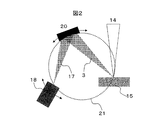
- One is a type in which the planar diffraction grating 16 of a multilayer film is rotated and the X-ray detector 18 is driven to detect and detect X-rays as shown in FIG.
- an X-ray condenser lens 19 is installed between the sample 15 and the diffraction grating 16 (for example, Patent Document 1).
- a slit may be provided between the sample 15 and the diffraction grating 16 in order to make the X-ray 3 incident on the diffraction grating 16 parallel.
- the other type is provided with a curved diffraction grating 20 called a Johann or Johansson type and a detector 18, and the curved diffraction grating 20 and the detector 18 are driven on a Roland circle while driving the X-ray.
- a type that detects light by spectroscopy Is a type that detects light by spectroscopy.
- Patent Document 2 in order to make a compact X-ray detection system, a diffraction crystal with unequal spacing is used for a spectroscopic crystal, X-rays are obliquely incident on the unequal spacing diffraction grating, and the spectrum is split by the unequal spacing diffraction grating. Multiple diffracted lights are detected simultaneously on a CCD detector.
- a machine that has a plurality of diffraction gratings and switches and replaces and installs the diffraction gratings so that the diffraction gratings can be selected and installed according to the X-ray energy to be analyzed.
- a special mechanism is provided.
- a WDX apparatus using a non-uniformly spaced diffraction grating and a position detector such as a CCD acquires an X-ray spectrum serving as a reference for an energy position and an X-ray spectrum to be evaluated. Then, the energy value of the X-ray spectrum to be evaluated is obtained from the relative amount of the reference X-ray spectrum energy position.
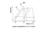
- FIG. 4 is a drawing examined by the inventors of the present application prior to the invention in order to explain the problems of the present application.
- the diffraction grating 22 having a shape that can obtain the maximum X-ray intensity of the X-ray energy E2 to be evaluated is used.
- the X-ray intensity of the reference X-ray energy E1 is significantly reduced.
- the intensity of the X-ray spectrum used as the energy position reference is small, the energy calibration of the X-ray spectrum to be evaluated becomes insufficient, and the measurement accuracy decreases.
- the intensity of the line spectrum increases, on the contrary, the intensity of the X-ray spectrum to be evaluated decreases, so that the measurement sensitivity similarly decreases.
- the CCD detection position in the direction perpendicular to the diffraction grating surface corresponds to the X-ray energy
- the X-ray detection position shift on the CCD accompanying the shift of the diffraction grating position shifts the X-ray energy position. Therefore, the elemental analysis corresponding to the X-ray energy position and the analysis accuracy of the electronic state are lowered.
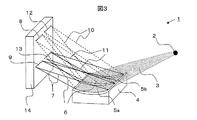
- the spectroscopic element according to the present invention includes a first pattern that separates the irradiated X-rays as a spectrum, and a second pattern that generates a spectrum different from the first pattern for the irradiated X-rays. It is characterized by that.
- the charged particle beam apparatus of the present invention includes an irradiation optical system that irradiates a sample with a charged particle beam, and an X-ray detection system that detects X-rays generated from the sample, and the X-ray detection system Comprises a spectroscopic element having a first pattern that separates the X-rays as a spectrum and a second pattern that causes the X-rays to generate a spectrum different from the first pattern. To do.
- the charged particle beam apparatus detects an electron optical system that irradiates an inspection sample with an electron beam, and detects secondary electrons generated from a portion irradiated with the electron beam, or detects electrons transmitted and scattered through the inspection sample. And a position detector that detects X-rays dispersed by the diffraction grating, and an X-ray spectroscopic element (hereinafter referred to as a diffraction grating) that separates X-rays generated from the portion irradiated with the electron beam. It has become.
- a first and a second plurality of patterns for generating different spectra for X-rays incident on the diffraction grating are formed in one diffraction grating.
- the first and second pattern shapes are characterized in that they are formed on the basis of the respective intensities of the X-ray reflectivity serving as a reference for the energy position and the X-ray reflectivity of the measurement object.
- the X-ray as a reference of the energy position is diffracted with the maximum reflectance
- the X-ray to be evaluated is diffracted with the maximum reflectance, and each X-ray having high X-ray intensity
- the line intensity distribution can be detected simultaneously by the position detector.
- This increases the sensitivity to the X-rays to be evaluated and the energy position accuracy of the X-rays, so that high-precision evaluation such as elemental analysis sensitivity and electronic state analysis in the sample becomes possible.
- the present invention eliminates the time loss by eliminating the need for highly accurate position adjustment of the diffraction grating. Therefore, high-precision elemental analysis is possible in a short period of time.
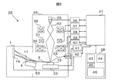
- FIG. 5 is a schematic diagram illustrating a configuration example of the electron beam analyzer 25 according to the first embodiment.
- An electron beam analyzer 25 shown in FIG. 5 includes a scanning electron microscope device 26, an X-ray analyzer 1, a control system 27, and an operation unit 28.
- the scanning electron microscope 26 includes an electron gun 29, a condenser lens 30, an electron beam deflector 31, an objective lens 32, a sample stage 33, and a secondary electron detector 35.
- the X-ray analyzer 1 includes a diffraction grating 4 and an X-ray position detector 14.
- the control system 27 includes an electron gun control unit 36, a condenser lens control unit 37, an electron beam deflector control unit 38, an objective lens control unit 39, a secondary electron detection system circuit control unit 40, a stage control unit 41, and an X-ray detection.
- the system circuit control unit 42 is configured.
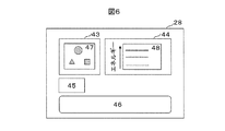
- the operation unit 28 includes an image display unit 43, an X-ray image and X-ray spectrum display unit 44, a storage unit 45 that stores a stage position, a secondary electron image, an X-ray image, a spectrum, and the like, and an operation screen 46.
- the X-ray analysis apparatus 1 and the scanning electron microscope apparatus 26 may be integrated as one apparatus, but are separable within a range in which the function of the X-ray analysis apparatus 1 is fulfilled. Needless to say.
- the primary electron beam 61 generated from the electron gun unit 29 is irradiated to the aperture sample 15 by the objective lens 32, and when the sample 15 is irradiated, the scanning speed and the scanning area are limited by the deflector 31.
- the secondary electrons 34 generated from the irradiated portion of the primary electron beam 61 are detected by the secondary electron detector 35 according to the scanning speed.
- the secondary electron signal detected by the secondary electron detector 35 is output in synchronization with the scanning signal of the primary electron beam 61, so that the secondary electron image of the sample 15 is displayed on the image display unit 43. 47 can be displayed.
- the X-ray analyzer 1 the X-ray 3 generated from the portion irradiated with the primary electron beam 61 is incident on the diffraction grating 4 to be dispersed, and the X-ray 17 dispersed by the diffraction grating 4 is detected in the X-ray position. Detect with detector 14. The position / angle adjustment of the diffraction grating 4 is adjusted by the diffraction grating position / rotation adjustment mechanism 62.
- the detected X-ray displays an X-ray image 48 on the X-ray image and spectrum display unit 44.
- the integral or average of the X-ray intensity is taken in the direction perpendicular to the X-ray energy axis, the X-ray energy is plotted on the horizontal axis, and the integrated value or average value of the X-ray intensity. Can be displayed on the X-ray image or the X-ray spectrum display unit 44.
- the X-rays of the X-ray intensity distributions 50a, 50b, and 50c in the X-ray image 48 correspond to 51a, 51b, and 51c in the X-ray spectrum 49, respectively.
- a part of the X-ray intensity (for example, 50a) in the X-ray intensity distribution 50 detected by the X-ray position detector 14 is selected, and an X-ray signal (50a) is selected.
- the image display unit 43 is provided with two screens so that the secondary electron image 47 and the element map image 52 can be displayed simultaneously.
- the X-ray 10 and the X-ray 11 separated by the second pattern 5b also have a linear X-ray intensity distribution 12 and an X-ray distribution 13 as in the case of the spectroscopy by the first pattern 5a.
- the first and second pattern shapes are also characterized in that they are formed based on the respective intensities of the X-ray reflectivity serving as a reference for the energy position and the X-ray reflectivity of the measurement target.
- the first pattern 5a and the second pattern 5b are formed with two patterns for convenience.
- the two patterns are not necessarily limited to two or more.
- a pattern may be formed.
- the ratio of the area of each pattern is the same in FIG. 3, more preferable detection sensitivity can be obtained by determining the ratio of each area based on the ratio at which the X-ray reflectivity or X-ray intensity to be measured is optimally obtained. be able to.
- 9A and 9B show examples of cross-sectional views of the first pattern 5a and the second pattern 5b in the diffraction grating 4 shown in FIG.
- the first pattern of the diffraction grating shown in FIG. 9A and the second pattern shown in FIG. 9B have a diffraction grating pattern shape called a sawtooth groove type blaze type.
- 9A and 9B show the pattern shape of the flat type at equal intervals for the sake of convenience.
- the concave shape and the irregularly spaced diffraction grating pattern are first used. And used in the second pattern.
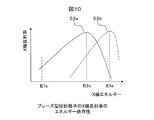
- Fig. 10 shows the X-ray energy dependence of the blaze-type X-ray reflectivity.
- the X-ray reflectivity dependence of the X-ray reflectivity under the condition that the saw blade inclination angle ⁇ B, called the blaze angle is ⁇ 1B (first pattern 5a) and ⁇ 2B (second pattern 5b) is the curve 53a, It is a curve 53b.
- the blaze angle ⁇ B of the first pattern 5a is set to ⁇ 1B at which the X-ray reflectivity to be evaluated of the X-ray energy E2a is maximized.
- the blaze angle ⁇ B of the second pattern 5b is set to ⁇ 2B at which the X-ray reflectivity of the energy E3a serving as the X-ray energy reference is maximized.
- the X-ray reflectivity of the blazed diffraction grating pattern is changed by changing the blaze angle.
- a diffraction grating pattern of another shape may be used.
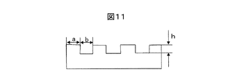
- X can also be changed by changing the height or groove depth of the rectangular portion (h in FIG. 11) and the widths of the convex and concave portions (a and b in FIG. 11). It is possible to change the line reflectivity. Further, X-ray reflection can be changed by changing the material used for the pattern or the material of the film coating the pattern. As described above, any spectroscopic element having a pattern for splitting X-rays can be applied to the present invention regardless of the spectroscopic method or the type of diffraction grating.
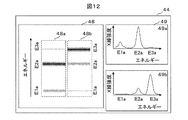
- each of the X-rays 3 incident on the diffraction grating 4 is split by the first pattern 5 a and the second pattern 5 b formed on the diffraction grating 4 and detected by the X-ray position detector 14.
- the X-ray images have image distributions such as an X-ray image 48a and an X-ray image 48b, respectively.
- the X-ray intensity is strong at the location of the X-ray energy E2a to be evaluated
- the X-ray intensity is strong at the location E3a that is the X-ray energy reference.
- X-ray spectra in which the X-ray energy is plotted on the horizontal axis and the integral value or average value of the X-ray image intensity is plotted on the vertical axis are the X-ray spectrum 49a and the X-ray spectrum 49b, respectively.
- the spectrum display unit 44 can be displayed.
- the energy E2a of the spectrum to be evaluated can be accurately evaluated from the reference energy E3a spectrum by the X-ray image 48b or the X-ray spectrum 49b.
- the intensity of the spectrum to be evaluated for the energy E2a is sufficiently high. Therefore, in addition to highly sensitive evaluation of element concentration, high evaluation such as evaluation of electronic structure reflected in the shape of the spectrum. Accurate evaluation became possible.
- an analysis electron microscope equipped with an X-ray apparatus provided with a diffraction grating formed with a plurality of patterns can simultaneously detect an X-ray spectrum serving as an energy reference and an X-ray spectrum to be evaluated, It was possible to detect with high spectral intensity.
- FIG. 13 shows the X-ray analyzer 1 mounted on the scanning transmission electron microscope 26a.
- the basic configuration is the same as that in which the X-ray analyzer 1 is mounted on the scanning electron microscope 26 shown in FIG. 5, but the electron beam analyzer 25a is generated by irradiating the sample 15 with the electron beam 61.
- X-ray condenser lens 56 for obtaining X-ray 3 with high yield, X-lens holding unit 57 for holding the X-ray lens, X-ray lens driving unit 58 for driving the X-ray lens 56, X-ray An X-ray lens drive control unit 59 for controlling the lens drive unit 58 is provided.
- the X-ray lens 56 for obtaining the X-rays with high yield is not described in the first embodiment, the X-ray lens 56 may be mounted on the scanning electron microscope 26 for implementation.
- the sample 15 is irradiated with the electron beam 61, and the electrons 60 transmitted and scattered through the sample 15 are detected.
- a transmission scattering electron detector 54 is installed below the sample 15.
- a signal obtained by the transmission / scattering electron detector 54 is subjected to signal processing by the transmission / scattering electron detection system circuit unit 55.
- the transmitted / scattered electron image of the sample 15 can be displayed on the image display unit 43.
- the intensity of the scattered electrons is proportional to the atomic number (Z) contained in the sample, and is therefore called a Z contrast image.
- the objective lens 32 is composed of an upper magnetic pole 32a and a lower magnetic pole 32b, and the X-ray lens 56 for taking in X-rays is between the objective lens upper magnetic pole 32a and the lower magnetic pole 32b.
- Install Due to the limitation of the space between the objective lens upper magnetic pole 32a and the lower magnetic pole 32b, there is a case in which the diameter of the X-ray condensing lens 56 is increased. The yield of X-rays can be increased by bringing the condenser lens 56 closer to the sample 15.
- the primary electron beam probe diameter can be reduced smaller than that of the scanning electron microscope 26. For this reason, since the electron beam analyzer 25a in which the X-ray analyzer 1a is mounted on the scanning transmission electron microscope 26a can irradiate a finer region with an electron beam, it is possible to detect an element with a trace amount and high energy as in the first embodiment. It became possible to perform analysis with higher resolution with higher spatial resolution.
Landscapes
- Analytical Chemistry (AREA)
- Chemical & Material Sciences (AREA)
- Physics & Mathematics (AREA)
- General Engineering & Computer Science (AREA)
- High Energy & Nuclear Physics (AREA)
- Engineering & Computer Science (AREA)
- Spectroscopy & Molecular Physics (AREA)
- Health & Medical Sciences (AREA)
- Life Sciences & Earth Sciences (AREA)
- Biochemistry (AREA)
- General Health & Medical Sciences (AREA)
- General Physics & Mathematics (AREA)
- Immunology (AREA)
- Pathology (AREA)
- Analysing Materials By The Use Of Radiation (AREA)
Abstract
Description
(実施の形態1)
図5は、本実施例1における電子線分析装置25の構成例を示す概略図である。図5に示す電子線分析装置25は、走査電子顕微鏡装置26、X線分析装置1、制御系27、操作部28より構成される。走査電子顕微鏡26は、電子銃29、コンデンサレンズ30、電子線偏向器31、対物レンズ32、試料ステージ33、二次電子検出器35により構成される。X線分析装置1は、回折格子4、X線位置検出器14により構成される。
(実施の形態2)
本実施例では、X線分析装置を走査透過電子顕微鏡(STEM)に搭載した例について説明する。
Claims (15)
- 照射したX線をスペクトルに分光する第1のパターンと、
前記照射したX線に対し、前記第1のパターンとは異なるスペクトルを生じさせる第2のパターンと、を有する
ことを特徴とする分光素子。 - 請求項1に記載の分光素子において、
前記第1のパターンが延在する方向に前記第2のパターンが設けられる
ことを特徴とする分光素子。 - 請求項1に記載の分光素子において、
前記第1のパターンの形状は、エネルギー基準となるX線反射率に基づいて定められ、
前記第2のパターンの形状は、評価対象のX線反射率に基づいて定められる
ことを特徴とする分光素子。 - 請求項1に記載の分光素子において、
前記第1のパターンの材質またはコーティング膜の材質は、エネルギー基準となるX線反射率に基づいて定められ、
前記第2のパターンの材質またはコーティング膜の材質は、評価対象のX線反射率に基づいて定められる
ことを特徴とする分光素子。 - 請求項1に記載の分光素子において、
前記第1のパターンと前記第2のパターンとの面積比は、エネルギー基準となるX線反射率と評価対象のX線反射率とに基づいて定められる
ことを特徴とする分光素子。 - 請求項1に記載の分光素子において、
前記第1のパターン及び前記第2のパターンはデザインルールプロセスにより設けられる
ことを特徴とする分光素子。 - 請求項1に記載の分光素子において、
前記第1のパターン及び前記第2のパターンは同一平面または同一曲面上に設けられる
ことを特徴とする分光素子。 - 請求項1に記載の分光素子において、
前記X線の照射領域内に前記第1のパターン及び前記第2のパターンが設けられる
ことを特徴とする分光素子。 - 試料に対し荷電粒子線を照射する照射光学系と、
前記試料から発生するX線を検出するX線検出系と、を有し、
前記X線検出系は、
前記X線をスペクトルに分光する第1のパターンと、
前記X線に対し、前記第1のパターンとは異なるスペクトルを生じさせる第2のパターンと、を有する分光素子を有する
ことを特徴とする荷電粒子線装置。 - 請求項9に記載の荷電粒子線装置において、
前記第2のパターンは、前記第1のパターンが延在する方向に設けられる
ことを特徴とする荷電粒子線装置。 - 請求項9に記載の荷電粒子線装置において、
前記第1のパターンの形状は、エネルギー基準となるX線反射率に基づいて定められ、
前記第2のパターンの形状は、評価対象のX線反射率に基づいて定めらる
ことを特徴とする荷電粒子線装置。 - 請求項9に記載の荷電粒子線装置において、
前記第1のパターンと前記第2のパターンとの面積比は、エネルギー基準となるX線反射率と評価対象のX線反射率とに基づいて定められる
ことを特徴とする荷電粒子線装置。 - 請求項9に記載の荷電粒子線装置において、
前記第1のパターン及び前記第2のパターンはデザインルールプロセスにより設けられる
ことを特徴とする荷電粒子線装置。 - 請求項9に記載の荷電粒子線装置において、
前記試料と前記分光素子との光路上に設置されたX線レンズを有する
ことを特徴とする荷電粒子線装置。 - 請求項14に記載の荷電粒子線装置において、
前記X線レンズを前記試料と前記分光素子との光路の範囲内で移動させる制御部を有する
ことを特徴とする荷電粒子線装置。
Priority Applications (3)
| Application Number | Priority Date | Filing Date | Title |
|---|---|---|---|
| JP2014544109A JP6025857B2 (ja) | 2012-10-31 | 2012-10-31 | 分光素子、およびそれを用いた荷電粒子線装置 |
| PCT/JP2012/078092 WO2014068689A1 (ja) | 2012-10-31 | 2012-10-31 | 分光素子、およびそれを用いた荷電粒子線装置 |
| US14/439,993 US9601308B2 (en) | 2012-10-31 | 2012-10-31 | Spectroscopic element and charged particle beam device using the same |
Applications Claiming Priority (1)
| Application Number | Priority Date | Filing Date | Title |
|---|---|---|---|
| PCT/JP2012/078092 WO2014068689A1 (ja) | 2012-10-31 | 2012-10-31 | 分光素子、およびそれを用いた荷電粒子線装置 |
Publications (1)
| Publication Number | Publication Date |
|---|---|
| WO2014068689A1 true WO2014068689A1 (ja) | 2014-05-08 |
Family
ID=50626659
Family Applications (1)
| Application Number | Title | Priority Date | Filing Date |
|---|---|---|---|
| PCT/JP2012/078092 Ceased WO2014068689A1 (ja) | 2012-10-31 | 2012-10-31 | 分光素子、およびそれを用いた荷電粒子線装置 |
Country Status (3)
| Country | Link |
|---|---|
| US (1) | US9601308B2 (ja) |
| JP (1) | JP6025857B2 (ja) |
| WO (1) | WO2014068689A1 (ja) |
Cited By (2)
| Publication number | Priority date | Publication date | Assignee | Title |
|---|---|---|---|---|
| JP2021162310A (ja) * | 2020-03-30 | 2021-10-11 | 日本電子株式会社 | 分析方法および分析装置 |
| US11353414B2 (en) * | 2019-03-08 | 2022-06-07 | Jeol Ltd. | Analysis device and spectrum generation method |
Families Citing this family (4)
| Publication number | Priority date | Publication date | Assignee | Title |
|---|---|---|---|---|
| JP6286535B2 (ja) * | 2014-05-30 | 2018-02-28 | 株式会社日立製作所 | 荷電粒子線分析装置および分析方法 |
| JP6998034B2 (ja) * | 2017-07-25 | 2022-01-18 | 株式会社日立ハイテクサイエンス | 放射線分析装置 |
| EP3502674A1 (en) * | 2017-12-19 | 2019-06-26 | Koninklijke Philips N.V. | Testing of curved x-ray gratings |
| EP3603516A1 (de) * | 2018-08-02 | 2020-02-05 | Siemens Healthcare GmbH | Röntgenvorrichtung und verfahren zum betrieb der röntgenvorrichtung |
Citations (3)
| Publication number | Priority date | Publication date | Assignee | Title |
|---|---|---|---|---|
| JPH0225800A (ja) * | 1988-07-14 | 1990-01-29 | Toshiba Corp | 波長可変x線集光器 |
| JPH03111799A (ja) * | 1989-09-26 | 1991-05-13 | Olympus Optical Co Ltd | 多層膜分光器 |
| JP2002189004A (ja) * | 2000-12-21 | 2002-07-05 | Jeol Ltd | X線分析装置 |
Family Cites Families (12)
| Publication number | Priority date | Publication date | Assignee | Title |
|---|---|---|---|---|
| JPH083558B2 (ja) * | 1988-01-29 | 1996-01-17 | 株式会社島津製作所 | X線分光器 |
| JPH1010299A (ja) * | 1996-06-26 | 1998-01-16 | Ishikawajima Harima Heavy Ind Co Ltd | 非対称角型分光器 |
| JPH11295245A (ja) * | 1998-04-10 | 1999-10-29 | Rigaku Industrial Co | X線分光素子およびそれを用いたx線分析装置 |
| US7655482B2 (en) * | 2000-04-18 | 2010-02-02 | Kla-Tencor | Chemical mechanical polishing test structures and methods for inspecting the same |
| JP2002329473A (ja) | 2001-02-27 | 2002-11-15 | Jeol Ltd | X線分光器を備えた透過型電子顕微鏡 |
| JP4161763B2 (ja) | 2003-03-26 | 2008-10-08 | 株式会社島津製作所 | 微小部分析用x線分光器および微小部分析用x線分光器の位置調整方法 |
| JP2009047586A (ja) * | 2007-08-21 | 2009-03-05 | Jeol Ltd | 化学結合状態分析を行うx線分析装置 |
| JP2009141058A (ja) * | 2007-12-05 | 2009-06-25 | Fujitsu Microelectronics Ltd | 半導体装置およびその製造方法 |
| JP5506345B2 (ja) * | 2009-11-26 | 2014-05-28 | 株式会社日立ハイテクノロジーズ | 荷電粒子線顕微鏡および当該荷電粒子顕微鏡の制御方法 |
| JP5768308B2 (ja) * | 2011-03-31 | 2015-08-26 | 住友電工ハードメタル株式会社 | 表面被覆切削工具 |
| KR101999988B1 (ko) * | 2012-03-08 | 2019-07-15 | 앱파이브 엘엘씨 | 고 공간 분해능에서 물질의 스트레인을 측정하기 위한 시스템 및 공정 |
| US9748683B2 (en) * | 2013-03-29 | 2017-08-29 | Kobe Steel, Ltd. | Electroconductive material superior in resistance to fretting corrosion for connection component |
-
2012
- 2012-10-31 US US14/439,993 patent/US9601308B2/en not_active Expired - Fee Related
- 2012-10-31 WO PCT/JP2012/078092 patent/WO2014068689A1/ja not_active Ceased
- 2012-10-31 JP JP2014544109A patent/JP6025857B2/ja not_active Expired - Fee Related
Patent Citations (3)
| Publication number | Priority date | Publication date | Assignee | Title |
|---|---|---|---|---|
| JPH0225800A (ja) * | 1988-07-14 | 1990-01-29 | Toshiba Corp | 波長可変x線集光器 |
| JPH03111799A (ja) * | 1989-09-26 | 1991-05-13 | Olympus Optical Co Ltd | 多層膜分光器 |
| JP2002189004A (ja) * | 2000-12-21 | 2002-07-05 | Jeol Ltd | X線分析装置 |
Cited By (3)
| Publication number | Priority date | Publication date | Assignee | Title |
|---|---|---|---|---|
| US11353414B2 (en) * | 2019-03-08 | 2022-06-07 | Jeol Ltd. | Analysis device and spectrum generation method |
| JP2021162310A (ja) * | 2020-03-30 | 2021-10-11 | 日本電子株式会社 | 分析方法および分析装置 |
| JP7144475B2 (ja) | 2020-03-30 | 2022-09-29 | 日本電子株式会社 | 分析方法および分析装置 |
Also Published As
| Publication number | Publication date |
|---|---|
| JP6025857B2 (ja) | 2016-11-16 |
| US9601308B2 (en) | 2017-03-21 |
| US20150318144A1 (en) | 2015-11-05 |
| JPWO2014068689A1 (ja) | 2016-09-08 |
Similar Documents
| Publication | Publication Date | Title |
|---|---|---|
| JP7573349B2 (ja) | 小角x線散乱計測計 | |
| KR102696675B1 (ko) | X-선 작은 각 산란측정을 위한 웨이퍼 정렬 | |
| JP6025857B2 (ja) | 分光素子、およびそれを用いた荷電粒子線装置 | |
| JP5307504B2 (ja) | X線分析装置及びx線分析方法 | |
| TWI392866B (zh) | 用於檢驗一樣本的設備及方法 | |
| KR20220129635A (ko) | 복합 오버레이 계측 타겟 | |
| JP2005207982A (ja) | 分光器及びそれを用いた測定装置 | |
| TWI862819B (zh) | 疊對計量系統及方法 | |
| US11473901B2 (en) | Height measurement device in which optical paths projected on the sample at different incidence angles | |
| CN116593509A (zh) | X射线衍射装置及测定方法 | |
| JP6503145B2 (ja) | 置換サイト計測装置および置換サイト計測方法 | |
| JP6198406B2 (ja) | マイクロ回折方法及び装置 | |
| JP2023061041A (ja) | 蛍光x線分析装置および蛍光x線分析方法 | |
| JP2009222727A (ja) | 分光器 | |
| JP2016031271A (ja) | X線分光器の調整方法、x線分光器、および試料分析装置 | |
| JP4365687B2 (ja) | 分析方法及び分析装置 |
Legal Events
| Date | Code | Title | Description |
|---|---|---|---|
| 121 | Ep: the epo has been informed by wipo that ep was designated in this application |
Ref document number: 12887713 Country of ref document: EP Kind code of ref document: A1 |
|
| ENP | Entry into the national phase |
Ref document number: 2014544109 Country of ref document: JP Kind code of ref document: A |
|
| NENP | Non-entry into the national phase |
Ref country code: DE |
|
| WWE | Wipo information: entry into national phase |
Ref document number: 14439993 Country of ref document: US |
|
| 122 | Ep: pct application non-entry in european phase |
Ref document number: 12887713 Country of ref document: EP Kind code of ref document: A1 |