WO2014051232A1 - 유기광전자소자용 화합물, 이를 포함하는 유기발광소자 및 상기 유기발광소자를 포함하는 표시장치 - Google Patents
유기광전자소자용 화합물, 이를 포함하는 유기발광소자 및 상기 유기발광소자를 포함하는 표시장치 Download PDFInfo
- Publication number
- WO2014051232A1 WO2014051232A1 PCT/KR2013/003897 KR2013003897W WO2014051232A1 WO 2014051232 A1 WO2014051232 A1 WO 2014051232A1 KR 2013003897 W KR2013003897 W KR 2013003897W WO 2014051232 A1 WO2014051232 A1 WO 2014051232A1
- Authority
- WO
- WIPO (PCT)
- Prior art keywords
- substituted
- unsubstituted
- group
- formula
- organic
- Prior art date
Links
- 150000001875 compounds Chemical class 0.000 title claims abstract description 125
- 230000005693 optoelectronics Effects 0.000 title claims abstract description 72
- 239000000126 substance Substances 0.000 claims abstract description 10
- 239000000463 material Substances 0.000 claims description 55
- 125000003118 aryl group Chemical group 0.000 claims description 51
- 238000002347 injection Methods 0.000 claims description 44
- 239000007924 injection Substances 0.000 claims description 44
- 125000000008 (C1-C10) alkyl group Chemical group 0.000 claims description 37
- 125000001072 heteroaryl group Chemical group 0.000 claims description 37
- YZCKVEUIGOORGS-OUBTZVSYSA-N Deuterium Chemical group [2H] YZCKVEUIGOORGS-OUBTZVSYSA-N 0.000 claims description 35
- 229910052805 deuterium Inorganic materials 0.000 claims description 35
- 229910052739 hydrogen Inorganic materials 0.000 claims description 35
- 239000001257 hydrogen Substances 0.000 claims description 35
- 150000002431 hydrogen Chemical group 0.000 claims description 34
- 238000012937 correction Methods 0.000 claims description 32
- 125000001424 substituent group Chemical group 0.000 claims description 28
- 238000000034 method Methods 0.000 claims description 27
- 230000005525 hole transport Effects 0.000 claims description 26
- 239000010409 thin film Substances 0.000 claims description 25
- -1 aryl group compound Chemical class 0.000 claims description 13
- 125000004450 alkenylene group Chemical group 0.000 claims description 7
- 125000004419 alkynylene group Chemical group 0.000 claims description 7
- 125000000732 arylene group Chemical group 0.000 claims description 6
- 230000005284 excitation Effects 0.000 claims description 6
- 125000005549 heteroarylene group Chemical group 0.000 claims description 6
- 125000005842 heteroatom Chemical group 0.000 claims description 6
- 230000000903 blocking effect Effects 0.000 claims description 4
- 239000010410 layer Substances 0.000 description 130
- YMWUJEATGCHHMB-UHFFFAOYSA-N Dichloromethane Chemical compound ClCCl YMWUJEATGCHHMB-UHFFFAOYSA-N 0.000 description 120
- 238000006243 chemical reaction Methods 0.000 description 104
- CSNNHWWHGAXBCP-UHFFFAOYSA-L Magnesium sulfate Chemical compound [Mg+2].[O-][S+2]([O-])([O-])[O-] CSNNHWWHGAXBCP-UHFFFAOYSA-L 0.000 description 96
- 239000000543 intermediate Substances 0.000 description 91
- 239000000243 solution Substances 0.000 description 90
- VLKZOEOYAKHREP-UHFFFAOYSA-N n-Hexane Chemical compound CCCCCC VLKZOEOYAKHREP-UHFFFAOYSA-N 0.000 description 85
- RTZKZFJDLAIYFH-UHFFFAOYSA-N Diethyl ether Chemical compound CCOCC RTZKZFJDLAIYFH-UHFFFAOYSA-N 0.000 description 84
- YXFVVABEGXRONW-UHFFFAOYSA-N Toluene Chemical compound CC1=CC=CC=C1 YXFVVABEGXRONW-UHFFFAOYSA-N 0.000 description 78
- 239000012299 nitrogen atmosphere Substances 0.000 description 65
- XEKOWRVHYACXOJ-UHFFFAOYSA-N Ethyl acetate Chemical compound CCOC(C)=O XEKOWRVHYACXOJ-UHFFFAOYSA-N 0.000 description 63
- WYURNTSHIVDZCO-UHFFFAOYSA-N Tetrahydrofuran Chemical compound C1CCOC1 WYURNTSHIVDZCO-UHFFFAOYSA-N 0.000 description 58
- XLYOFNOQVPJJNP-UHFFFAOYSA-N water Chemical compound O XLYOFNOQVPJJNP-UHFFFAOYSA-N 0.000 description 49
- 239000012153 distilled water Substances 0.000 description 48
- 239000000706 filtrate Substances 0.000 description 48
- 229910052943 magnesium sulfate Inorganic materials 0.000 description 48
- 235000019341 magnesium sulphate Nutrition 0.000 description 48
- 239000000203 mixture Substances 0.000 description 43
- 239000007864 aqueous solution Substances 0.000 description 37
- 239000000047 product Substances 0.000 description 33
- 238000010898 silica gel chromatography Methods 0.000 description 32
- 230000015572 biosynthetic process Effects 0.000 description 30
- 238000003786 synthesis reaction Methods 0.000 description 30
- YLQBMQCUIZJEEH-UHFFFAOYSA-N tetrahydrofuran Natural products C=1C=COC=1 YLQBMQCUIZJEEH-UHFFFAOYSA-N 0.000 description 29
- 239000012044 organic layer Substances 0.000 description 27
- 238000003756 stirring Methods 0.000 description 26
- BWHMMNNQKKPAPP-UHFFFAOYSA-L potassium carbonate Chemical compound [K+].[K+].[O-]C([O-])=O BWHMMNNQKKPAPP-UHFFFAOYSA-L 0.000 description 24
- NLXLAEXVIDQMFP-UHFFFAOYSA-N Ammonia chloride Chemical compound [NH4+].[Cl-] NLXLAEXVIDQMFP-UHFFFAOYSA-N 0.000 description 18
- KZMGYPLQYOPHEL-UHFFFAOYSA-N Boron trifluoride etherate Chemical compound FB(F)F.CCOCC KZMGYPLQYOPHEL-UHFFFAOYSA-N 0.000 description 18
- UIIMBOGNXHQVGW-UHFFFAOYSA-M Sodium bicarbonate Chemical compound [Na+].OC([O-])=O UIIMBOGNXHQVGW-UHFFFAOYSA-M 0.000 description 18
- BWHDROKFUHTORW-UHFFFAOYSA-N tritert-butylphosphane Chemical compound CC(C)(C)P(C(C)(C)C)C(C)(C)C BWHDROKFUHTORW-UHFFFAOYSA-N 0.000 description 18
- CSCPPACGZOOCGX-UHFFFAOYSA-N Acetone Chemical compound CC(C)=O CSCPPACGZOOCGX-UHFFFAOYSA-N 0.000 description 15
- 125000000217 alkyl group Chemical group 0.000 description 15
- 238000001816 cooling Methods 0.000 description 13
- 238000010992 reflux Methods 0.000 description 13
- 239000000284 extract Substances 0.000 description 12
- NFHFRUOZVGFOOS-UHFFFAOYSA-N palladium;triphenylphosphane Chemical compound [Pd].C1=CC=CC=C1P(C=1C=CC=CC=1)C1=CC=CC=C1.C1=CC=CC=C1P(C=1C=CC=CC=1)C1=CC=CC=C1.C1=CC=CC=C1P(C=1C=CC=CC=1)C1=CC=CC=C1.C1=CC=CC=C1P(C=1C=CC=CC=1)C1=CC=CC=C1 NFHFRUOZVGFOOS-UHFFFAOYSA-N 0.000 description 12
- 229910000027 potassium carbonate Inorganic materials 0.000 description 12
- MZRVEZGGRBJDDB-UHFFFAOYSA-N N-Butyllithium Chemical compound [Li]CCCC MZRVEZGGRBJDDB-UHFFFAOYSA-N 0.000 description 10
- 239000002019 doping agent Substances 0.000 description 10
- 239000011368 organic material Substances 0.000 description 10
- 238000002360 preparation method Methods 0.000 description 10
- 235000019270 ammonium chloride Nutrition 0.000 description 9
- NXPHGHWWQRMDIA-UHFFFAOYSA-M magnesium;carbanide;bromide Chemical compound [CH3-].[Mg+2].[Br-] NXPHGHWWQRMDIA-UHFFFAOYSA-M 0.000 description 9
- 235000017557 sodium bicarbonate Nutrition 0.000 description 9
- 229910000030 sodium bicarbonate Inorganic materials 0.000 description 9
- 230000008859 change Effects 0.000 description 7
- 238000011161 development Methods 0.000 description 7
- 230000018109 developmental process Effects 0.000 description 7
- 125000000524 functional group Chemical group 0.000 description 7
- 239000007787 solid Substances 0.000 description 7
- OKKJLVBELUTLKV-UHFFFAOYSA-N Methanol Chemical compound OC OKKJLVBELUTLKV-UHFFFAOYSA-N 0.000 description 6
- KWYHDKDOAIKMQN-UHFFFAOYSA-N N,N,N',N'-tetramethylethylenediamine Chemical compound CN(C)CCN(C)C KWYHDKDOAIKMQN-UHFFFAOYSA-N 0.000 description 6
- 125000003277 amino group Chemical group 0.000 description 6
- WRECIMRULFAWHA-UHFFFAOYSA-N trimethyl borate Chemical compound COB(OC)OC WRECIMRULFAWHA-UHFFFAOYSA-N 0.000 description 6
- SPDPTFAJSFKAMT-UHFFFAOYSA-N 1-n-[4-[4-(n-[4-(3-methyl-n-(3-methylphenyl)anilino)phenyl]anilino)phenyl]phenyl]-4-n,4-n-bis(3-methylphenyl)-1-n-phenylbenzene-1,4-diamine Chemical group CC1=CC=CC(N(C=2C=CC(=CC=2)N(C=2C=CC=CC=2)C=2C=CC(=CC=2)C=2C=CC(=CC=2)N(C=2C=CC=CC=2)C=2C=CC(=CC=2)N(C=2C=C(C)C=CC=2)C=2C=C(C)C=CC=2)C=2C=C(C)C=CC=2)=C1 SPDPTFAJSFKAMT-UHFFFAOYSA-N 0.000 description 5
- JAUCIDPGGHZXRP-UHFFFAOYSA-N 4-phenyl-n-(4-phenylphenyl)aniline Chemical compound C=1C=C(C=2C=CC=CC=2)C=CC=1NC(C=C1)=CC=C1C1=CC=CC=C1 JAUCIDPGGHZXRP-UHFFFAOYSA-N 0.000 description 5
- DGAQECJNVWCQMB-PUAWFVPOSA-M Ilexoside XXIX Chemical compound C[C@@H]1CC[C@@]2(CC[C@@]3(C(=CC[C@H]4[C@]3(CC[C@@H]5[C@@]4(CC[C@@H](C5(C)C)OS(=O)(=O)[O-])C)C)[C@@H]2[C@]1(C)O)C)C(=O)O[C@H]6[C@@H]([C@H]([C@@H]([C@H](O6)CO)O)O)O.[Na+] DGAQECJNVWCQMB-PUAWFVPOSA-M 0.000 description 5
- 230000000052 comparative effect Effects 0.000 description 5
- BIECSXCXIXHDBC-UHFFFAOYSA-N methyl 2-bromo-5-chlorobenzoate Chemical compound COC(=O)C1=CC(Cl)=CC=C1Br BIECSXCXIXHDBC-UHFFFAOYSA-N 0.000 description 5
- 229960005235 piperonyl butoxide Drugs 0.000 description 5
- 229910052708 sodium Inorganic materials 0.000 description 5
- 239000011734 sodium Substances 0.000 description 5
- 239000000758 substrate Substances 0.000 description 5
- XLOMVQKBTHCTTD-UHFFFAOYSA-N Zinc monoxide Chemical compound [Zn]=O XLOMVQKBTHCTTD-UHFFFAOYSA-N 0.000 description 4
- 230000008901 benefit Effects 0.000 description 4
- 125000004432 carbon atom Chemical group C* 0.000 description 4
- 230000000694 effects Effects 0.000 description 4
- 239000010408 film Substances 0.000 description 4
- 238000005259 measurement Methods 0.000 description 4
- 229910052751 metal Inorganic materials 0.000 description 4
- 239000002184 metal Substances 0.000 description 4
- SWGQITQOBPXVRC-UHFFFAOYSA-N methyl 2-bromobenzoate Chemical compound COC(=O)C1=CC=CC=C1Br SWGQITQOBPXVRC-UHFFFAOYSA-N 0.000 description 4
- 229910052757 nitrogen Inorganic materials 0.000 description 4
- OKTJSMMVPCPJKN-UHFFFAOYSA-N Carbon Chemical group [C] OKTJSMMVPCPJKN-UHFFFAOYSA-N 0.000 description 3
- KFZMGEQAYNKOFK-UHFFFAOYSA-N Isopropanol Chemical compound CC(C)O KFZMGEQAYNKOFK-UHFFFAOYSA-N 0.000 description 3
- 125000005103 alkyl silyl group Chemical group 0.000 description 3
- 235000010210 aluminium Nutrition 0.000 description 3
- 239000011575 calcium Substances 0.000 description 3
- 229910052799 carbon Inorganic materials 0.000 description 3
- 125000004093 cyano group Chemical group *C#N 0.000 description 3
- 125000000753 cycloalkyl group Chemical group 0.000 description 3
- 125000003983 fluorenyl group Chemical group C1(=CC=CC=2C3=CC=CC=C3CC12)* 0.000 description 3
- 125000001153 fluoro group Chemical group F* 0.000 description 3
- 230000005283 ground state Effects 0.000 description 3
- 238000004770 highest occupied molecular orbital Methods 0.000 description 3
- AMGQUBHHOARCQH-UHFFFAOYSA-N indium;oxotin Chemical compound [In].[Sn]=O AMGQUBHHOARCQH-UHFFFAOYSA-N 0.000 description 3
- 125000005647 linker group Chemical group 0.000 description 3
- 238000004768 lowest unoccupied molecular orbital Methods 0.000 description 3
- 238000004519 manufacturing process Methods 0.000 description 3
- 150000002739 metals Chemical class 0.000 description 3
- 239000007773 negative electrode material Substances 0.000 description 3
- 125000000449 nitro group Chemical group [O-][N+](*)=O 0.000 description 3
- 229910052760 oxygen Inorganic materials 0.000 description 3
- 125000005561 phenanthryl group Chemical group 0.000 description 3
- 125000003808 silyl group Chemical group [H][Si]([H])([H])[*] 0.000 description 3
- 125000000999 tert-butyl group Chemical group [H]C([H])([H])C(*)(C([H])([H])[H])C([H])([H])[H] 0.000 description 3
- 230000007704 transition Effects 0.000 description 3
- TVIVIEFSHFOWTE-UHFFFAOYSA-K tri(quinolin-8-yloxy)alumane Chemical compound [Al+3].C1=CN=C2C([O-])=CC=CC2=C1.C1=CN=C2C([O-])=CC=CC2=C1.C1=CN=C2C([O-])=CC=CC2=C1 TVIVIEFSHFOWTE-UHFFFAOYSA-K 0.000 description 3
- 125000004950 trifluoroalkyl group Chemical group 0.000 description 3
- 125000002023 trifluoromethyl group Chemical group FC(F)(F)* 0.000 description 3
- 238000001771 vacuum deposition Methods 0.000 description 3
- YJTKZCDBKVTVBY-UHFFFAOYSA-N 1,3-Diphenylbenzene Chemical group C1=CC=CC=C1C1=CC=CC(C=2C=CC=CC=2)=C1 YJTKZCDBKVTVBY-UHFFFAOYSA-N 0.000 description 2
- NHDODQWIKUYWMW-UHFFFAOYSA-N 1-bromo-4-chlorobenzene Chemical compound ClC1=CC=C(Br)C=C1 NHDODQWIKUYWMW-UHFFFAOYSA-N 0.000 description 2
- RUFPHBVGCFYCNW-UHFFFAOYSA-N 1-naphthylamine Chemical compound C1=CC=C2C(N)=CC=CC2=C1 RUFPHBVGCFYCNW-UHFFFAOYSA-N 0.000 description 2
- SDTMFDGELKWGFT-UHFFFAOYSA-N 2-methylpropan-2-olate Chemical compound CC(C)(C)[O-] SDTMFDGELKWGFT-UHFFFAOYSA-N 0.000 description 2
- QENGPZGAWFQWCZ-UHFFFAOYSA-N 3-Methylthiophene Chemical compound CC=1C=CSC=1 QENGPZGAWFQWCZ-UHFFFAOYSA-N 0.000 description 2
- VIZUPBYFLORCRA-UHFFFAOYSA-N 9,10-dinaphthalen-2-ylanthracene Chemical compound C12=CC=CC=C2C(C2=CC3=CC=CC=C3C=C2)=C(C=CC=C2)C2=C1C1=CC=C(C=CC=C2)C2=C1 VIZUPBYFLORCRA-UHFFFAOYSA-N 0.000 description 2
- IJGRMHOSHXDMSA-UHFFFAOYSA-N Atomic nitrogen Chemical compound N#N IJGRMHOSHXDMSA-UHFFFAOYSA-N 0.000 description 2
- FIPWRIJSWJWJAI-UHFFFAOYSA-N Butyl carbitol 6-propylpiperonyl ether Chemical compound C1=C(CCC)C(COCCOCCOCCCC)=CC2=C1OCO2 FIPWRIJSWJWJAI-UHFFFAOYSA-N 0.000 description 2
- 0 CC1(C)c2cc(N(c(c(Sc3c4)c5)ccc5-c5ccccc5)c3ccc4-c3ccccc3)ccc2-c2c1ccc1c2*c2ccccc2C1(C)C Chemical compound CC1(C)c2cc(N(c(c(Sc3c4)c5)ccc5-c5ccccc5)c3ccc4-c3ccccc3)ccc2-c2c1ccc1c2*c2ccccc2C1(C)C 0.000 description 2
- VTYYLEPIZMXCLO-UHFFFAOYSA-L Calcium carbonate Chemical compound [Ca+2].[O-]C([O-])=O VTYYLEPIZMXCLO-UHFFFAOYSA-L 0.000 description 2
- PXHVJJICTQNCMI-UHFFFAOYSA-N Nickel Chemical compound [Ni] PXHVJJICTQNCMI-UHFFFAOYSA-N 0.000 description 2
- XYFCBTPGUUZFHI-UHFFFAOYSA-N Phosphine Chemical compound P XYFCBTPGUUZFHI-UHFFFAOYSA-N 0.000 description 2
- YTPLMLYBLZKORZ-UHFFFAOYSA-N Thiophene Chemical compound C=1C=CSC=1 YTPLMLYBLZKORZ-UHFFFAOYSA-N 0.000 description 2
- 125000000641 acridinyl group Chemical group C1(=CC=CC2=NC3=CC=CC=C3C=C12)* 0.000 description 2
- 229910045601 alloy Inorganic materials 0.000 description 2
- 239000000956 alloy Substances 0.000 description 2
- 229910052782 aluminium Inorganic materials 0.000 description 2
- XAGFODPZIPBFFR-UHFFFAOYSA-N aluminium Chemical compound [Al] XAGFODPZIPBFFR-UHFFFAOYSA-N 0.000 description 2
- 150000001412 amines Chemical class 0.000 description 2
- 125000002178 anthracenyl group Chemical group C1(=CC=CC2=CC3=CC=CC=C3C=C12)* 0.000 description 2
- 125000004653 anthracenylene group Chemical group 0.000 description 2
- 125000003785 benzimidazolyl group Chemical group N1=C(NC2=C1C=CC=C2)* 0.000 description 2
- 125000000499 benzofuranyl group Chemical group O1C(=CC2=C1C=CC=C2)* 0.000 description 2
- 125000004196 benzothienyl group Chemical group S1C(=CC2=C1C=CC=C2)* 0.000 description 2
- 125000004622 benzoxazinyl group Chemical group O1NC(=CC2=C1C=CC=C2)* 0.000 description 2
- DMVOXQPQNTYEKQ-UHFFFAOYSA-N biphenyl-4-amine Chemical group C1=CC(N)=CC=C1C1=CC=CC=C1 DMVOXQPQNTYEKQ-UHFFFAOYSA-N 0.000 description 2
- 125000002529 biphenylenyl group Chemical group C1(=CC=CC=2C3=CC=CC=C3C12)* 0.000 description 2
- 125000000609 carbazolyl group Chemical class C1(=CC=CC=2C3=CC=CC=C3NC12)* 0.000 description 2
- 239000011203 carbon fibre reinforced carbon Substances 0.000 description 2
- 125000002676 chrysenyl group Chemical group C1(=CC=CC=2C3=CC=C4C=CC=CC4=C3C=CC12)* 0.000 description 2
- 239000003086 colorant Substances 0.000 description 2
- 230000021615 conjugation Effects 0.000 description 2
- 238000002425 crystallisation Methods 0.000 description 2
- 230000008025 crystallization Effects 0.000 description 2
- 230000007423 decrease Effects 0.000 description 2
- 238000000151 deposition Methods 0.000 description 2
- TXCDCPKCNAJMEE-UHFFFAOYSA-N dibenzofuran Chemical compound C1=CC=C2C3=CC=CC=C3OC2=C1 TXCDCPKCNAJMEE-UHFFFAOYSA-N 0.000 description 2
- IYYZUPMFVPLQIF-UHFFFAOYSA-N dibenzothiophene Chemical compound C1=CC=C2C3=CC=CC=C3SC2=C1 IYYZUPMFVPLQIF-UHFFFAOYSA-N 0.000 description 2
- USIUVYZYUHIAEV-UHFFFAOYSA-N diphenyl ether Chemical compound C=1C=CC=CC=1OC1=CC=CC=C1 USIUVYZYUHIAEV-UHFFFAOYSA-N 0.000 description 2
- 125000001495 ethyl group Chemical group [H]C([H])([H])C([H])([H])* 0.000 description 2
- NIHNNTQXNPWCJQ-UHFFFAOYSA-N fluorene Chemical compound C1=CC=C2CC3=CC=CC=C3C2=C1 NIHNNTQXNPWCJQ-UHFFFAOYSA-N 0.000 description 2
- 125000005567 fluorenylene group Chemical group 0.000 description 2
- 125000002541 furyl group Chemical group 0.000 description 2
- 108700039708 galantide Proteins 0.000 description 2
- 229910052736 halogen Inorganic materials 0.000 description 2
- 150000002367 halogens Chemical class 0.000 description 2
- 125000002887 hydroxy group Chemical group [H]O* 0.000 description 2
- 125000002883 imidazolyl group Chemical group 0.000 description 2
- 125000003454 indenyl group Chemical group C1(C=CC2=CC=CC=C12)* 0.000 description 2
- 125000001041 indolyl group Chemical group 0.000 description 2
- 125000000959 isobutyl group Chemical group [H]C([H])([H])C([H])(C([H])([H])[H])C([H])([H])* 0.000 description 2
- 125000001449 isopropyl group Chemical group [H]C([H])([H])C([H])(*)C([H])([H])[H] 0.000 description 2
- 125000002183 isoquinolinyl group Chemical group C1(=NC=CC2=CC=CC=C12)* 0.000 description 2
- 230000007246 mechanism Effects 0.000 description 2
- 239000012528 membrane Substances 0.000 description 2
- 125000002496 methyl group Chemical group [H]C([H])([H])* 0.000 description 2
- KDADHQHDRSAQDY-UHFFFAOYSA-N n-(4-phenylphenyl)naphthalen-1-amine Chemical compound C=1C=CC2=CC=CC=C2C=1NC(C=C1)=CC=C1C1=CC=CC=C1 KDADHQHDRSAQDY-UHFFFAOYSA-N 0.000 description 2
- 125000001624 naphthyl group Chemical group 0.000 description 2
- 125000004957 naphthylene group Chemical group 0.000 description 2
- 125000004593 naphthyridinyl group Chemical group N1=C(C=CC2=CC=CN=C12)* 0.000 description 2
- 230000003287 optical effect Effects 0.000 description 2
- 125000002971 oxazolyl group Chemical group 0.000 description 2
- IIENVBUXFRSCLM-UHFFFAOYSA-N phenoxathiin-4-ylboronic acid Chemical compound S1C2=CC=CC=C2OC2=C1C=CC=C2B(O)O IIENVBUXFRSCLM-UHFFFAOYSA-N 0.000 description 2
- 125000001997 phenyl group Chemical group [H]C1=C([H])C([H])=C(*)C([H])=C1[H] 0.000 description 2
- 125000000843 phenylene group Chemical group C1(=C(C=CC=C1)*)* 0.000 description 2
- 229910052698 phosphorus Inorganic materials 0.000 description 2
- BASFCYQUMIYNBI-UHFFFAOYSA-N platinum Chemical compound [Pt] BASFCYQUMIYNBI-UHFFFAOYSA-N 0.000 description 2
- 125000001436 propyl group Chemical group [H]C([*])([H])C([H])([H])C([H])([H])[H] 0.000 description 2
- 125000003373 pyrazinyl group Chemical group 0.000 description 2
- 125000003226 pyrazolyl group Chemical group 0.000 description 2
- 125000005548 pyrenylene group Chemical group 0.000 description 2
- 125000004076 pyridyl group Chemical group 0.000 description 2
- 125000000714 pyrimidinyl group Chemical group 0.000 description 2
- 125000000168 pyrrolyl group Chemical group 0.000 description 2
- 125000002294 quinazolinyl group Chemical group N1=C(N=CC2=CC=CC=C12)* 0.000 description 2
- 125000002943 quinolinyl group Chemical group N1=C(C=CC2=CC=CC=C12)* 0.000 description 2
- 125000001567 quinoxalinyl group Chemical group N1=C(C=NC2=CC=CC=C12)* 0.000 description 2
- 230000004044 response Effects 0.000 description 2
- 239000004332 silver Substances 0.000 description 2
- MFRIHAYPQRLWNB-UHFFFAOYSA-N sodium tert-butoxide Chemical compound [Na+].CC(C)(C)[O-] MFRIHAYPQRLWNB-UHFFFAOYSA-N 0.000 description 2
- 238000004528 spin coating Methods 0.000 description 2
- 229910052717 sulfur Inorganic materials 0.000 description 2
- 125000001935 tetracenyl group Chemical group C1(=CC=CC2=CC3=CC4=CC=CC=C4C=C3C=C12)* 0.000 description 2
- 125000001113 thiadiazolyl group Chemical group 0.000 description 2
- 125000000335 thiazolyl group Chemical group 0.000 description 2
- 125000001544 thienyl group Chemical group 0.000 description 2
- 125000004306 triazinyl group Chemical group 0.000 description 2
- 125000001425 triazolyl group Chemical group 0.000 description 2
- 125000003960 triphenylenyl group Chemical group C1(=CC=CC=2C3=CC=CC=C3C3=CC=CC=C3C12)* 0.000 description 2
- 238000005406 washing Methods 0.000 description 2
- 239000011787 zinc oxide Substances 0.000 description 2
- 125000004169 (C1-C6) alkyl group Chemical group 0.000 description 1
- IBGUDZMIAZLJNY-UHFFFAOYSA-N 1,4-dibromonaphthalene Chemical compound C1=CC=C2C(Br)=CC=C(Br)C2=C1 IBGUDZMIAZLJNY-UHFFFAOYSA-N 0.000 description 1
- XJKSTNDFUHDPQJ-UHFFFAOYSA-N 1,4-diphenylbenzene Chemical group C1=CC=CC=C1C1=CC=C(C=2C=CC=CC=2)C=C1 XJKSTNDFUHDPQJ-UHFFFAOYSA-N 0.000 description 1
- IVYAYAWSXINSEF-UHFFFAOYSA-N 1-tert-butylperylene Chemical group C1=CC(C=2C(C(C)(C)C)=CC=C3C=2C2=CC=C3)=C3C2=CC=CC3=C1 IVYAYAWSXINSEF-UHFFFAOYSA-N 0.000 description 1
- BFTIPCRZWILUIY-UHFFFAOYSA-N 2,5,8,11-tetratert-butylperylene Chemical group CC(C)(C)C1=CC(C2=CC(C(C)(C)C)=CC=3C2=C2C=C(C=3)C(C)(C)C)=C3C2=CC(C(C)(C)C)=CC3=C1 BFTIPCRZWILUIY-UHFFFAOYSA-N 0.000 description 1
- MTVNAPYHLASOSX-UHFFFAOYSA-N 9,9-dimethylxanthene Chemical compound C1=CC=C2C(C)(C)C3=CC=CC=C3OC2=C1 MTVNAPYHLASOSX-UHFFFAOYSA-N 0.000 description 1
- 239000004229 Alkannin Substances 0.000 description 1
- 108010017443 B 43 Proteins 0.000 description 1
- 229910016036 BaF 2 Inorganic materials 0.000 description 1
- HBEJZAFTUFBPQL-UHFFFAOYSA-N Bc(cccc1C2(C)C)c1Sc1c2cccc1 Chemical compound Bc(cccc1C2(C)C)c1Sc1c2cccc1 HBEJZAFTUFBPQL-UHFFFAOYSA-N 0.000 description 1
- DQZNCPLQHYVLSD-UHFFFAOYSA-N C(CC=C1)C2C1c1ccccc1CC2N(C1C=CC(c2ccccc2)=CC1)c(cc1)ccc1-c1cccc2c1Sc1c(C3C=CC=CC3C3(C4C=CC=CC4)C4C=CC=CC4)c3ccc1O2 Chemical compound C(CC=C1)C2C1c1ccccc1CC2N(C1C=CC(c2ccccc2)=CC1)c(cc1)ccc1-c1cccc2c1Sc1c(C3C=CC=CC3C3(C4C=CC=CC4)C4C=CC=CC4)c3ccc1O2 DQZNCPLQHYVLSD-UHFFFAOYSA-N 0.000 description 1
- HKRRASXRZRAAMF-UHFFFAOYSA-N C1C=CC(C2(C3C=CC=CC3C3=C4OC5C(C6C=CC(N(C7C(CCC=C8)=C8C=CC7)c7ccccc7)=CC6)=CC=CC5OC4=CCC23)C2=CCCC=C2)=CC1 Chemical compound C1C=CC(C2(C3C=CC=CC3C3=C4OC5C(C6C=CC(N(C7C(CCC=C8)=C8C=CC7)c7ccccc7)=CC6)=CC=CC5OC4=CCC23)C2=CCCC=C2)=CC1 HKRRASXRZRAAMF-UHFFFAOYSA-N 0.000 description 1
- XHNRMDCMRQPQTH-UHFFFAOYSA-N C1C=CC=CC1c(cc1)ccc1Nc(cc1)ccc1-c1ccccc1 Chemical compound C1C=CC=CC1c(cc1)ccc1Nc(cc1)ccc1-c1ccccc1 XHNRMDCMRQPQTH-UHFFFAOYSA-N 0.000 description 1
- VMJCNCPYMLLLOE-UHFFFAOYSA-N CC(C)(C1=C2C=CCC1)C(CC1)=C2C2=C1Sc(cccc1-c(cc3C4C=C(C5NC=CCC5)C=CC44)ccc3N4C3C=CC=CC3)c1S2 Chemical compound CC(C)(C1=C2C=CCC1)C(CC1)=C2C2=C1Sc(cccc1-c(cc3C4C=C(C5NC=CCC5)C=CC44)ccc3N4C3C=CC=CC3)c1S2 VMJCNCPYMLLLOE-UHFFFAOYSA-N 0.000 description 1
- QMFQSAQWKZLWHM-UHFFFAOYSA-N CC(C)(C1C2C=CCC1)C(CC1)=C2C2=C1Sc1cccc(-c(c3c4cccc3)ccc4N(C(CC3)=CC=C3C3=CC=CCC3)c(cc3)ccc3-c3ccccc3)c1C2 Chemical compound CC(C)(C1C2C=CCC1)C(CC1)=C2C2=C1Sc1cccc(-c(c3c4cccc3)ccc4N(C(CC3)=CC=C3C3=CC=CCC3)c(cc3)ccc3-c3ccccc3)c1C2 QMFQSAQWKZLWHM-UHFFFAOYSA-N 0.000 description 1
- NWBNNGRRNRWWES-UHFFFAOYSA-N CC(C)(C1C=CC=CC1c1c2C3=C)c1ccc2SC1C3C(c(cc2)ccc2N(C2CCCCC2)C2=CCCC3C=CCCC23)=CCC1 Chemical compound CC(C)(C1C=CC=CC1c1c2C3=C)c1ccc2SC1C3C(c(cc2)ccc2N(C2CCCCC2)C2=CCCC3C=CCCC23)=CCC1 NWBNNGRRNRWWES-UHFFFAOYSA-N 0.000 description 1
- LFVKMWJWIPQNER-UHFFFAOYSA-N CC1(C)C(C=C(CC2)c3cc(-c4c5[s]c(cccc6)c6c5ccc4)ccc3)=C2c2c1ccc1c2CCc2ccccc2[Si]1(C)C Chemical compound CC1(C)C(C=C(CC2)c3cc(-c4c5[s]c(cccc6)c6c5ccc4)ccc3)=C2c2c1ccc1c2CCc2ccccc2[Si]1(C)C LFVKMWJWIPQNER-UHFFFAOYSA-N 0.000 description 1
- KKEHJKKWDPIUMG-UHFFFAOYSA-N CC1(C)C(C=C(CC2)c3ccc(CC(c4ccccc4)c4c-5cccc4)c-5c3)=C2c2c1ccc1c2Sc2ccccc2C1(C)C Chemical compound CC1(C)C(C=C(CC2)c3ccc(CC(c4ccccc4)c4c-5cccc4)c-5c3)=C2c2c1ccc1c2Sc2ccccc2C1(C)C KKEHJKKWDPIUMG-UHFFFAOYSA-N 0.000 description 1
- STGXMABLARDDMJ-UHFFFAOYSA-N CC1(C)C(C=CC2SC3=CCCC(C(C=C4)=C5C=CCCC5C4Br)=C3OC22)=C2c2c1cccc2 Chemical compound CC1(C)C(C=CC2SC3=CCCC(C(C=C4)=C5C=CCCC5C4Br)=C3OC22)=C2c2c1cccc2 STGXMABLARDDMJ-UHFFFAOYSA-N 0.000 description 1
- SAEAIDZFRNXFHS-UHFFFAOYSA-N CC1(C)C(C=CCC2)=C2C2=C1CCC(Sc1ccc3)=C2Sc1c3-c(cc1)cc(C2C=CC=CC22)c1N2C1NC(C2CC=CCC2)=CC(C2=CC=CCC2)N1 Chemical compound CC1(C)C(C=CCC2)=C2C2=C1CCC(Sc1ccc3)=C2Sc1c3-c(cc1)cc(C2C=CC=CC22)c1N2C1NC(C2CC=CCC2)=CC(C2=CC=CCC2)N1 SAEAIDZFRNXFHS-UHFFFAOYSA-N 0.000 description 1
- QRSAOYGHVKJMNS-UHFFFAOYSA-N CC1(C)C2=CC(C(CC34)=CC=C3c3c5OC(C=CCC6)=C6Nc5ccc3C4(C3C=CC=CC3)C3C=CC=CC3)=CCC2C2C(Nc3ccccc3CC3)=C3C=CC12 Chemical compound CC1(C)C2=CC(C(CC34)=CC=C3c3c5OC(C=CCC6)=C6Nc5ccc3C4(C3C=CC=CC3)C3C=CC=CC3)=CCC2C2C(Nc3ccccc3CC3)=C3C=CC12 QRSAOYGHVKJMNS-UHFFFAOYSA-N 0.000 description 1
- LUZXHOCSZZWUJX-UHFFFAOYSA-N CC1(C)C2C=CCCC2C2=C3SC4C(c(cc5)c(cccc6)c6c5N(C5C=CC=CC5)c(cc5)ccc5C5=CCCC=C5)=CC=CC4OC3=CCC12 Chemical compound CC1(C)C2C=CCCC2C2=C3SC4C(c(cc5)c(cccc6)c6c5N(C5C=CC=CC5)c(cc5)ccc5C5=CCCC=C5)=CC=CC4OC3=CCC12 LUZXHOCSZZWUJX-UHFFFAOYSA-N 0.000 description 1
- NXNMZKIAVSEFCZ-UHFFFAOYSA-N CC1(C)c(cc(cc2)-c3cc(-c4c5[o]c(cccc6)c6c5ccc4)ccc3)c2-c2c1ccc1c2Sc2ccccc2[Si]1(C)C Chemical compound CC1(C)c(cc(cc2)-c3cc(-c4c5[o]c(cccc6)c6c5ccc4)ccc3)c2-c2c1ccc1c2Sc2ccccc2[Si]1(C)C NXNMZKIAVSEFCZ-UHFFFAOYSA-N 0.000 description 1
- QDCOFXWTLOYAAP-UHFFFAOYSA-N CC1(C)c(cc(cc2)-c3nc(-c4ccccc4)nc(-c4ccccc4)n3)c2-c2c3Sc(cccc4)c4[Si](c4ccccc4)(C4=CCCC=C4)c3ccc12 Chemical compound CC1(C)c(cc(cc2)-c3nc(-c4ccccc4)nc(-c4ccccc4)n3)c2-c2c3Sc(cccc4)c4[Si](c4ccccc4)(C4=CCCC=C4)c3ccc12 QDCOFXWTLOYAAP-UHFFFAOYSA-N 0.000 description 1
- AWTNYQQIYOHVIT-UHFFFAOYSA-N CC1(C)c2cc(-c3cc(-c4ncccc4)cc(-c4ncccc4)c3)ccc2-c2c1ccc1c2Sc2ccccc2C1(c1ccccc1)c1ccccc1 Chemical compound CC1(C)c2cc(-c3cc(-c4ncccc4)cc(-c4ncccc4)c3)ccc2-c2c1ccc1c2Sc2ccccc2C1(c1ccccc1)c1ccccc1 AWTNYQQIYOHVIT-UHFFFAOYSA-N 0.000 description 1
- SJOFBBWNYBRZSP-UHFFFAOYSA-N CC1(C)c2cc(-c3nc(cccc4)c4cc3)ccc2-c2c1ccc1c2Oc2ccccc2C1(c1ccccc1)c1ccccc1 Chemical compound CC1(C)c2cc(-c3nc(cccc4)c4cc3)ccc2-c2c1ccc1c2Oc2ccccc2C1(c1ccccc1)c1ccccc1 SJOFBBWNYBRZSP-UHFFFAOYSA-N 0.000 description 1
- VMYFBNYDZKDHKU-UHFFFAOYSA-N CC1(C)c2cc(C(CC3c4ccccc4)=Nc4c3cccc4)ccc2-c2c1ccc1c2Oc(cccc2)c2[Si]1(c1ccccc1)c1ccccc1 Chemical compound CC1(C)c2cc(C(CC3c4ccccc4)=Nc4c3cccc4)ccc2-c2c1ccc1c2Oc(cccc2)c2[Si]1(c1ccccc1)c1ccccc1 VMYFBNYDZKDHKU-UHFFFAOYSA-N 0.000 description 1
- QKTLNGKLNFXLKU-UHFFFAOYSA-N CC1(C)c2ccc3SC4C=CC=C(C(CC5)CC=C5N(C(CC5)C=CC5C5C=CCCC5)C5C=CC(c6ccccc6)=CC5)C4Cc3c2C2C1CCCC2 Chemical compound CC1(C)c2ccc3SC4C=CC=C(C(CC5)CC=C5N(C(CC5)C=CC5C5C=CCCC5)C5C=CC(c6ccccc6)=CC5)C4Cc3c2C2C1CCCC2 QKTLNGKLNFXLKU-UHFFFAOYSA-N 0.000 description 1
- XBDUAWCDNFZEEV-UHFFFAOYSA-N CC1(C)c2cccc(-c(cc3)ccc3N3C(C=CCC4)=C4C4C3C=CCC4)c2SC2=C1CCC1=C2c2ccccc2C1(C1=CCCCC1)C1=CCCC=C1 Chemical compound CC1(C)c2cccc(-c(cc3)ccc3N3C(C=CCC4)=C4C4C3C=CCC4)c2SC2=C1CCC1=C2c2ccccc2C1(C1=CCCCC1)C1=CCCC=C1 XBDUAWCDNFZEEV-UHFFFAOYSA-N 0.000 description 1
- MYXIUMODUXJNKQ-UHFFFAOYSA-N CC1(C)c2cccc(-c(cccc3)c3C(OC)=O)c2Sc2c1cccc2 Chemical compound CC1(C)c2cccc(-c(cccc3)c3C(OC)=O)c2Sc2c1cccc2 MYXIUMODUXJNKQ-UHFFFAOYSA-N 0.000 description 1
- UCUYUMHSNWAHIO-UHFFFAOYSA-N CC1(C)c2ccccc2C2=C1CCC1SC3=CC=CC(C4C=CC(C(CC=C5)c6c5c(cccc5)c5[s]6)=CC4)C3OC21 Chemical compound CC1(C)c2ccccc2C2=C1CCC1SC3=CC=CC(C4C=CC(C(CC=C5)c6c5c(cccc5)c5[s]6)=CC4)C3OC21 UCUYUMHSNWAHIO-UHFFFAOYSA-N 0.000 description 1
- OYPRJOBELJOOCE-UHFFFAOYSA-N Calcium Chemical compound [Ca] OYPRJOBELJOOCE-UHFFFAOYSA-N 0.000 description 1
- 239000004215 Carbon black (E152) Substances 0.000 description 1
- VYZAMTAEIAYCRO-UHFFFAOYSA-N Chromium Chemical compound [Cr] VYZAMTAEIAYCRO-UHFFFAOYSA-N 0.000 description 1
- RYGMFSIKBFXOCR-UHFFFAOYSA-N Copper Chemical compound [Cu] RYGMFSIKBFXOCR-UHFFFAOYSA-N 0.000 description 1
- 239000004214 Fast Green FCF Substances 0.000 description 1
- 239000004230 Fast Yellow AB Substances 0.000 description 1
- 108700042658 GAP-43 Proteins 0.000 description 1
- 108700032487 GAP-43-3 Proteins 0.000 description 1
- 229910052688 Gadolinium Inorganic materials 0.000 description 1
- 239000001922 Gum ghatti Substances 0.000 description 1
- UFHFLCQGNIYNRP-UHFFFAOYSA-N Hydrogen Chemical compound [H][H] UFHFLCQGNIYNRP-UHFFFAOYSA-N 0.000 description 1
- 239000004233 Indanthrene blue RS Substances 0.000 description 1
- WHXSMMKQMYFTQS-UHFFFAOYSA-N Lithium Chemical compound [Li] WHXSMMKQMYFTQS-UHFFFAOYSA-N 0.000 description 1
- FYYHWMGAXLPEAU-UHFFFAOYSA-N Magnesium Chemical compound [Mg] FYYHWMGAXLPEAU-UHFFFAOYSA-N 0.000 description 1
- LWLSVNFEVKJDBZ-UHFFFAOYSA-N N-[4-(trifluoromethoxy)phenyl]-4-[[3-[5-(trifluoromethyl)pyridin-2-yl]oxyphenyl]methyl]piperidine-1-carboxamide Chemical compound FC(OC1=CC=C(C=C1)NC(=O)N1CCC(CC1)CC1=CC(=CC=C1)OC1=NC=C(C=C1)C(F)(F)F)(F)F LWLSVNFEVKJDBZ-UHFFFAOYSA-N 0.000 description 1
- 239000004235 Orange GGN Substances 0.000 description 1
- 239000004218 Orcein Substances 0.000 description 1
- 239000004237 Ponceau 6R Substances 0.000 description 1
- 239000004236 Ponceau SX Substances 0.000 description 1
- ZLMJMSJWJFRBEC-UHFFFAOYSA-N Potassium Chemical compound [K] ZLMJMSJWJFRBEC-UHFFFAOYSA-N 0.000 description 1
- 239000004231 Riboflavin-5-Sodium Phosphate Substances 0.000 description 1
- BQCADISMDOOEFD-UHFFFAOYSA-N Silver Chemical compound [Ag] BQCADISMDOOEFD-UHFFFAOYSA-N 0.000 description 1
- 229910006404 SnO 2 Inorganic materials 0.000 description 1
- ATJFFYVFTNAWJD-UHFFFAOYSA-N Tin Chemical compound [Sn] ATJFFYVFTNAWJD-UHFFFAOYSA-N 0.000 description 1
- RTAQQCXQSZGOHL-UHFFFAOYSA-N Titanium Chemical compound [Ti] RTAQQCXQSZGOHL-UHFFFAOYSA-N 0.000 description 1
- 206010047571 Visual impairment Diseases 0.000 description 1
- 239000004234 Yellow 2G Substances 0.000 description 1
- HCHKCACWOHOZIP-UHFFFAOYSA-N Zinc Chemical compound [Zn] HCHKCACWOHOZIP-UHFFFAOYSA-N 0.000 description 1
- 239000006096 absorbing agent Substances 0.000 description 1
- 125000001931 aliphatic group Chemical group 0.000 description 1
- 235000019232 alkannin Nutrition 0.000 description 1
- 239000004191 allura red AC Substances 0.000 description 1
- 235000012741 allura red AC Nutrition 0.000 description 1
- 239000004411 aluminium Substances 0.000 description 1
- 239000004178 amaranth Substances 0.000 description 1
- 235000012735 amaranth Nutrition 0.000 description 1
- 239000010405 anode material Substances 0.000 description 1
- 239000004410 anthocyanin Substances 0.000 description 1
- 235000010208 anthocyanin Nutrition 0.000 description 1
- QVGXLLKOCUKJST-UHFFFAOYSA-N atomic oxygen Chemical compound [O] QVGXLLKOCUKJST-UHFFFAOYSA-N 0.000 description 1
- 239000004176 azorubin Substances 0.000 description 1
- 235000012733 azorubine Nutrition 0.000 description 1
- 229910052788 barium Inorganic materials 0.000 description 1
- DSAJWYNOEDNPEQ-UHFFFAOYSA-N barium atom Chemical compound [Ba] DSAJWYNOEDNPEQ-UHFFFAOYSA-N 0.000 description 1
- 239000001654 beetroot red Substances 0.000 description 1
- 235000012677 beetroot red Nutrition 0.000 description 1
- 125000006267 biphenyl group Chemical group 0.000 description 1
- 239000004126 brilliant black BN Substances 0.000 description 1
- 235000012709 brilliant black BN Nutrition 0.000 description 1
- 239000004161 brilliant blue FCF Substances 0.000 description 1
- 235000012745 brilliant blue FCF Nutrition 0.000 description 1
- 239000004109 brown FK Substances 0.000 description 1
- 235000012713 brown FK Nutrition 0.000 description 1
- 239000001678 brown HT Substances 0.000 description 1
- 235000012670 brown HT Nutrition 0.000 description 1
- 239000000872 buffer Substances 0.000 description 1
- 125000000484 butyl group Chemical group [H]C([*])([H])C([H])([H])C([H])([H])C([H])([H])[H] 0.000 description 1
- 229910052792 caesium Inorganic materials 0.000 description 1
- TVFDJXOCXUVLDH-UHFFFAOYSA-N caesium atom Chemical compound [Cs] TVFDJXOCXUVLDH-UHFFFAOYSA-N 0.000 description 1
- 229910052791 calcium Inorganic materials 0.000 description 1
- 235000010216 calcium carbonate Nutrition 0.000 description 1
- 235000019241 carbon black Nutrition 0.000 description 1
- CREMABGTGYGIQB-UHFFFAOYSA-N carbon carbon Chemical compound C.C CREMABGTGYGIQB-UHFFFAOYSA-N 0.000 description 1
- 239000004106 carminic acid Substances 0.000 description 1
- 235000012730 carminic acid Nutrition 0.000 description 1
- 239000010406 cathode material Substances 0.000 description 1
- 239000001752 chlorophylls and chlorophyllins Substances 0.000 description 1
- 235000012698 chlorophylls and chlorophyllins Nutrition 0.000 description 1
- 229910052804 chromium Inorganic materials 0.000 description 1
- 239000011651 chromium Substances 0.000 description 1
- 239000001679 citrus red 2 Substances 0.000 description 1
- 235000013986 citrus red 2 Nutrition 0.000 description 1
- 239000011248 coating agent Substances 0.000 description 1
- 238000000576 coating method Methods 0.000 description 1
- 229920001940 conductive polymer Polymers 0.000 description 1
- 239000004020 conductor Substances 0.000 description 1
- 229910052802 copper Inorganic materials 0.000 description 1
- 239000010949 copper Substances 0.000 description 1
- 239000004121 copper complexes of chlorophylls and chlorophyllins Substances 0.000 description 1
- 235000012700 copper complexes of chlorophylls and chlorophyllins Nutrition 0.000 description 1
- 239000004148 curcumin Substances 0.000 description 1
- 235000012754 curcumin Nutrition 0.000 description 1
- 125000004122 cyclic group Chemical group 0.000 description 1
- 125000001995 cyclobutyl group Chemical group [H]C1([H])C([H])([H])C([H])(*)C1([H])[H] 0.000 description 1
- 125000001511 cyclopentyl group Chemical group [H]C1([H])C([H])([H])C([H])([H])C([H])(*)C1([H])[H] 0.000 description 1
- 125000001559 cyclopropyl group Chemical group [H]C1([H])C([H])([H])C1([H])* 0.000 description 1
- 238000000354 decomposition reaction Methods 0.000 description 1
- 230000008021 deposition Effects 0.000 description 1
- 125000005509 dibenzothiophenyl group Chemical group 0.000 description 1
- LIKFHECYJZWXFJ-UHFFFAOYSA-N dimethyldichlorosilane Chemical compound C[Si](C)(Cl)Cl LIKFHECYJZWXFJ-UHFFFAOYSA-N 0.000 description 1
- 238000007598 dipping method Methods 0.000 description 1
- 238000009826 distribution Methods 0.000 description 1
- 239000007772 electrode material Substances 0.000 description 1
- 239000004174 erythrosine Substances 0.000 description 1
- 235000012732 erythrosine Nutrition 0.000 description 1
- 238000001704 evaporation Methods 0.000 description 1
- 230000008020 evaporation Effects 0.000 description 1
- 230000005281 excited state Effects 0.000 description 1
- 235000019240 fast green FCF Nutrition 0.000 description 1
- 235000019233 fast yellow AB Nutrition 0.000 description 1
- UIWYJDYFSGRHKR-UHFFFAOYSA-N gadolinium atom Chemical compound [Gd] UIWYJDYFSGRHKR-UHFFFAOYSA-N 0.000 description 1
- 239000011521 glass Substances 0.000 description 1
- 230000009477 glass transition Effects 0.000 description 1
- PCHJSUWPFVWCPO-UHFFFAOYSA-N gold Chemical compound [Au] PCHJSUWPFVWCPO-UHFFFAOYSA-N 0.000 description 1
- 229910052737 gold Inorganic materials 0.000 description 1
- 239000010931 gold Substances 0.000 description 1
- 235000010193 gold Nutrition 0.000 description 1
- 239000004333 gold (food color) Substances 0.000 description 1
- 239000004120 green S Substances 0.000 description 1
- 235000012701 green S Nutrition 0.000 description 1
- 125000005843 halogen group Chemical group 0.000 description 1
- 125000004051 hexyl group Chemical group [H]C([H])([H])C([H])([H])C([H])([H])C([H])([H])C([H])([H])C([H])([H])* 0.000 description 1
- 230000006872 improvement Effects 0.000 description 1
- 235000019239 indanthrene blue RS Nutrition 0.000 description 1
- 239000004179 indigotine Substances 0.000 description 1
- 235000012738 indigotine Nutrition 0.000 description 1
- 229910052738 indium Inorganic materials 0.000 description 1
- APFVFJFRJDLVQX-UHFFFAOYSA-N indium atom Chemical compound [In] APFVFJFRJDLVQX-UHFFFAOYSA-N 0.000 description 1
- 229910003437 indium oxide Inorganic materials 0.000 description 1
- PJXISJQVUVHSOJ-UHFFFAOYSA-N indium(iii) oxide Chemical compound [O-2].[O-2].[O-2].[In+3].[In+3] PJXISJQVUVHSOJ-UHFFFAOYSA-N 0.000 description 1
- 238000007641 inkjet printing Methods 0.000 description 1
- 230000003993 interaction Effects 0.000 description 1
- 230000009878 intermolecular interaction Effects 0.000 description 1
- 238000007733 ion plating Methods 0.000 description 1
- 239000004407 iron oxides and hydroxides Substances 0.000 description 1
- 235000010213 iron oxides and hydroxides Nutrition 0.000 description 1
- 239000004973 liquid crystal related substance Substances 0.000 description 1
- 229910052744 lithium Inorganic materials 0.000 description 1
- 239000004335 litholrubine BK Substances 0.000 description 1
- 235000010187 litholrubine BK Nutrition 0.000 description 1
- 229910052749 magnesium Inorganic materials 0.000 description 1
- 239000011777 magnesium Substances 0.000 description 1
- 238000000691 measurement method Methods 0.000 description 1
- 229910044991 metal oxide Inorganic materials 0.000 description 1
- 150000004706 metal oxides Chemical class 0.000 description 1
- BIFARHLBYAKSSN-UHFFFAOYSA-N methyl 2-bromo-4-chlorobenzoate Chemical compound COC(=O)C1=CC=C(Cl)C=C1Br BIFARHLBYAKSSN-UHFFFAOYSA-N 0.000 description 1
- 125000002950 monocyclic group Chemical group 0.000 description 1
- YGNUPJXMDOFFDO-UHFFFAOYSA-N n,4-diphenylaniline Chemical compound C=1C=C(C=2C=CC=CC=2)C=CC=1NC1=CC=CC=C1 YGNUPJXMDOFFDO-UHFFFAOYSA-N 0.000 description 1
- 125000004108 n-butyl group Chemical group [H]C([H])([H])C([H])([H])C([H])([H])C([H])([H])* 0.000 description 1
- 229910052759 nickel Inorganic materials 0.000 description 1
- 125000004433 nitrogen atom Chemical group N* 0.000 description 1
- 235000019236 orange GGN Nutrition 0.000 description 1
- 235000019248 orcein Nutrition 0.000 description 1
- 150000002894 organic compounds Chemical class 0.000 description 1
- 125000001715 oxadiazolyl group Chemical group 0.000 description 1
- 239000001301 oxygen Substances 0.000 description 1
- 239000004177 patent blue V Substances 0.000 description 1
- 235000012736 patent blue V Nutrition 0.000 description 1
- 125000001147 pentyl group Chemical group C(CCCC)* 0.000 description 1
- 125000001792 phenanthrenyl group Chemical group C1(=CC=CC=2C3=CC=CC=C3C=CC12)* 0.000 description 1
- 150000002990 phenothiazines Chemical class 0.000 description 1
- 229910000073 phosphorus hydride Inorganic materials 0.000 description 1
- 238000007747 plating Methods 0.000 description 1
- 229910052697 platinum Inorganic materials 0.000 description 1
- 229920000767 polyaniline Polymers 0.000 description 1
- 125000003367 polycyclic group Chemical group 0.000 description 1
- 229920000128 polypyrrole Polymers 0.000 description 1
- 239000004175 ponceau 4R Substances 0.000 description 1
- 235000012731 ponceau 4R Nutrition 0.000 description 1
- 235000019238 ponceau 6R Nutrition 0.000 description 1
- 235000019237 ponceau SX Nutrition 0.000 description 1
- 239000007774 positive electrode material Substances 0.000 description 1
- 229910052700 potassium Inorganic materials 0.000 description 1
- 239000011591 potassium Substances 0.000 description 1
- 125000001725 pyrenyl group Chemical group 0.000 description 1
- 239000004172 quinoline yellow Substances 0.000 description 1
- 235000012752 quinoline yellow Nutrition 0.000 description 1
- 230000006798 recombination Effects 0.000 description 1
- 238000005215 recombination Methods 0.000 description 1
- 239000004180 red 2G Substances 0.000 description 1
- 235000012739 red 2G Nutrition 0.000 description 1
- 230000001846 repelling effect Effects 0.000 description 1
- 230000027756 respiratory electron transport chain Effects 0.000 description 1
- 239000002151 riboflavin Substances 0.000 description 1
- 235000019234 riboflavin-5-sodium phosphate Nutrition 0.000 description 1
- 239000004248 saffron Substances 0.000 description 1
- 235000013974 saffron Nutrition 0.000 description 1
- 229920006395 saturated elastomer Polymers 0.000 description 1
- 125000002914 sec-butyl group Chemical group [H]C([H])([H])C([H])([H])C([H])(*)C([H])([H])[H] 0.000 description 1
- 239000004065 semiconductor Substances 0.000 description 1
- 229910052709 silver Inorganic materials 0.000 description 1
- 235000010191 silver Nutrition 0.000 description 1
- 239000002002 slurry Substances 0.000 description 1
- 239000002904 solvent Substances 0.000 description 1
- 238000004544 sputter deposition Methods 0.000 description 1
- 239000004173 sunset yellow FCF Substances 0.000 description 1
- 235000012751 sunset yellow FCF Nutrition 0.000 description 1
- 239000001648 tannin Substances 0.000 description 1
- 235000018553 tannin Nutrition 0.000 description 1
- 239000004149 tartrazine Substances 0.000 description 1
- 235000012756 tartrazine Nutrition 0.000 description 1
- 125000006836 terphenylene group Chemical group 0.000 description 1
- 238000005979 thermal decomposition reaction Methods 0.000 description 1
- 229930192474 thiophene Natural products 0.000 description 1
- YRHRIQCWCFGUEQ-UHFFFAOYSA-N thioxanthen-9-one Chemical compound C1=CC=C2C(=O)C3=CC=CC=C3SC2=C1 YRHRIQCWCFGUEQ-UHFFFAOYSA-N 0.000 description 1
- 229910052718 tin Inorganic materials 0.000 description 1
- 239000010936 titanium Substances 0.000 description 1
- 229910052719 titanium Inorganic materials 0.000 description 1
- 239000004408 titanium dioxide Substances 0.000 description 1
- 235000010215 titanium dioxide Nutrition 0.000 description 1
- 238000012546 transfer Methods 0.000 description 1
- JLTRXTDYQLMHGR-UHFFFAOYSA-N trimethylaluminium Chemical compound C[Al](C)C JLTRXTDYQLMHGR-UHFFFAOYSA-N 0.000 description 1
- 125000004417 unsaturated alkyl group Chemical group 0.000 description 1
- 229910052720 vanadium Inorganic materials 0.000 description 1
- GPPXJZIENCGNKB-UHFFFAOYSA-N vanadium Chemical compound [V]#[V] GPPXJZIENCGNKB-UHFFFAOYSA-N 0.000 description 1
- 239000004108 vegetable carbon Substances 0.000 description 1
- 235000012712 vegetable carbon Nutrition 0.000 description 1
- 235000019235 yellow 2G Nutrition 0.000 description 1
- 229910052727 yttrium Inorganic materials 0.000 description 1
- VWQVUPCCIRVNHF-UHFFFAOYSA-N yttrium atom Chemical compound [Y] VWQVUPCCIRVNHF-UHFFFAOYSA-N 0.000 description 1
- 229910052725 zinc Inorganic materials 0.000 description 1
- 239000011701 zinc Substances 0.000 description 1
- YVTHLONGBIQYBO-UHFFFAOYSA-N zinc indium(3+) oxygen(2-) Chemical compound [O--].[Zn++].[In+3] YVTHLONGBIQYBO-UHFFFAOYSA-N 0.000 description 1
Images


Classifications
-
- H—ELECTRICITY
- H10—SEMICONDUCTOR DEVICES; ELECTRIC SOLID-STATE DEVICES NOT OTHERWISE PROVIDED FOR
- H10K—ORGANIC ELECTRIC SOLID-STATE DEVICES
- H10K85/00—Organic materials used in the body or electrodes of devices covered by this subclass
- H10K85/60—Organic compounds having low molecular weight
- H10K85/649—Aromatic compounds comprising a hetero atom
- H10K85/657—Polycyclic condensed heteroaromatic hydrocarbons
-
- C—CHEMISTRY; METALLURGY
- C07—ORGANIC CHEMISTRY
- C07D—HETEROCYCLIC COMPOUNDS
- C07D311/00—Heterocyclic compounds containing six-membered rings having one oxygen atom as the only hetero atom, condensed with other rings
- C07D311/02—Heterocyclic compounds containing six-membered rings having one oxygen atom as the only hetero atom, condensed with other rings ortho- or peri-condensed with carbocyclic rings or ring systems
- C07D311/78—Ring systems having three or more relevant rings
-
- C—CHEMISTRY; METALLURGY
- C07—ORGANIC CHEMISTRY
- C07D—HETEROCYCLIC COMPOUNDS
- C07D319/00—Heterocyclic compounds containing six-membered rings having two oxygen atoms as the only ring hetero atoms
- C07D319/10—1,4-Dioxanes; Hydrogenated 1,4-dioxanes
- C07D319/14—1,4-Dioxanes; Hydrogenated 1,4-dioxanes condensed with carbocyclic rings or ring systems
- C07D319/24—[b,e]-condensed with two six-membered rings
-
- C—CHEMISTRY; METALLURGY
- C07—ORGANIC CHEMISTRY
- C07D—HETEROCYCLIC COMPOUNDS
- C07D327/00—Heterocyclic compounds containing rings having oxygen and sulfur atoms as the only ring hetero atoms
- C07D327/02—Heterocyclic compounds containing rings having oxygen and sulfur atoms as the only ring hetero atoms one oxygen atom and one sulfur atom
- C07D327/06—Six-membered rings
- C07D327/08—[b,e]-condensed with two six-membered carbocyclic rings
-
- C—CHEMISTRY; METALLURGY
- C07—ORGANIC CHEMISTRY
- C07D—HETEROCYCLIC COMPOUNDS
- C07D335/00—Heterocyclic compounds containing six-membered rings having one sulfur atom as the only ring hetero atom
- C07D335/04—Heterocyclic compounds containing six-membered rings having one sulfur atom as the only ring hetero atom condensed with carbocyclic rings or ring systems
- C07D335/10—Dibenzothiopyrans; Hydrogenated dibenzothiopyrans
- C07D335/12—Thioxanthenes
-
- C—CHEMISTRY; METALLURGY
- C07—ORGANIC CHEMISTRY
- C07D—HETEROCYCLIC COMPOUNDS
- C07D339/00—Heterocyclic compounds containing rings having two sulfur atoms as the only ring hetero atoms
- C07D339/08—Six-membered rings
-
- C—CHEMISTRY; METALLURGY
- C07—ORGANIC CHEMISTRY
- C07D—HETEROCYCLIC COMPOUNDS
- C07D405/00—Heterocyclic compounds containing both one or more hetero rings having oxygen atoms as the only ring hetero atoms, and one or more rings having nitrogen as the only ring hetero atom
- C07D405/02—Heterocyclic compounds containing both one or more hetero rings having oxygen atoms as the only ring hetero atoms, and one or more rings having nitrogen as the only ring hetero atom containing two hetero rings
- C07D405/04—Heterocyclic compounds containing both one or more hetero rings having oxygen atoms as the only ring hetero atoms, and one or more rings having nitrogen as the only ring hetero atom containing two hetero rings directly linked by a ring-member-to-ring-member bond
-
- C—CHEMISTRY; METALLURGY
- C07—ORGANIC CHEMISTRY
- C07D—HETEROCYCLIC COMPOUNDS
- C07D413/00—Heterocyclic compounds containing two or more hetero rings, at least one ring having nitrogen and oxygen atoms as the only ring hetero atoms
- C07D413/02—Heterocyclic compounds containing two or more hetero rings, at least one ring having nitrogen and oxygen atoms as the only ring hetero atoms containing two hetero rings
- C07D413/04—Heterocyclic compounds containing two or more hetero rings, at least one ring having nitrogen and oxygen atoms as the only ring hetero atoms containing two hetero rings directly linked by a ring-member-to-ring-member bond
-
- C—CHEMISTRY; METALLURGY
- C07—ORGANIC CHEMISTRY
- C07D—HETEROCYCLIC COMPOUNDS
- C07D417/00—Heterocyclic compounds containing two or more hetero rings, at least one ring having nitrogen and sulfur atoms as the only ring hetero atoms, not provided for by group C07D415/00
- C07D417/02—Heterocyclic compounds containing two or more hetero rings, at least one ring having nitrogen and sulfur atoms as the only ring hetero atoms, not provided for by group C07D415/00 containing two hetero rings
- C07D417/04—Heterocyclic compounds containing two or more hetero rings, at least one ring having nitrogen and sulfur atoms as the only ring hetero atoms, not provided for by group C07D415/00 containing two hetero rings directly linked by a ring-member-to-ring-member bond
-
- C—CHEMISTRY; METALLURGY
- C07—ORGANIC CHEMISTRY
- C07F—ACYCLIC, CARBOCYCLIC OR HETEROCYCLIC COMPOUNDS CONTAINING ELEMENTS OTHER THAN CARBON, HYDROGEN, HALOGEN, OXYGEN, NITROGEN, SULFUR, SELENIUM OR TELLURIUM
- C07F7/00—Compounds containing elements of Groups 4 or 14 of the Periodic System
- C07F7/02—Silicon compounds
- C07F7/08—Compounds having one or more C—Si linkages
- C07F7/0803—Compounds with Si-C or Si-Si linkages
- C07F7/0805—Compounds with Si-C or Si-Si linkages comprising only Si, C or H atoms
- C07F7/0807—Compounds with Si-C or Si-Si linkages comprising only Si, C or H atoms comprising Si as a ring atom
-
- C—CHEMISTRY; METALLURGY
- C07—ORGANIC CHEMISTRY
- C07F—ACYCLIC, CARBOCYCLIC OR HETEROCYCLIC COMPOUNDS CONTAINING ELEMENTS OTHER THAN CARBON, HYDROGEN, HALOGEN, OXYGEN, NITROGEN, SULFUR, SELENIUM OR TELLURIUM
- C07F7/00—Compounds containing elements of Groups 4 or 14 of the Periodic System
- C07F7/02—Silicon compounds
- C07F7/08—Compounds having one or more C—Si linkages
- C07F7/0803—Compounds with Si-C or Si-Si linkages
- C07F7/081—Compounds with Si-C or Si-Si linkages comprising at least one atom selected from the elements N, O, halogen, S, Se or Te
- C07F7/0812—Compounds with Si-C or Si-Si linkages comprising at least one atom selected from the elements N, O, halogen, S, Se or Te comprising a heterocyclic ring
- C07F7/0816—Compounds with Si-C or Si-Si linkages comprising at least one atom selected from the elements N, O, halogen, S, Se or Te comprising a heterocyclic ring said ring comprising Si as a ring atom
-
- C—CHEMISTRY; METALLURGY
- C09—DYES; PAINTS; POLISHES; NATURAL RESINS; ADHESIVES; COMPOSITIONS NOT OTHERWISE PROVIDED FOR; APPLICATIONS OF MATERIALS NOT OTHERWISE PROVIDED FOR
- C09K—MATERIALS FOR MISCELLANEOUS APPLICATIONS, NOT PROVIDED FOR ELSEWHERE
- C09K11/00—Luminescent, e.g. electroluminescent, chemiluminescent materials
- C09K11/06—Luminescent, e.g. electroluminescent, chemiluminescent materials containing organic luminescent materials
-
- H—ELECTRICITY
- H10—SEMICONDUCTOR DEVICES; ELECTRIC SOLID-STATE DEVICES NOT OTHERWISE PROVIDED FOR
- H10K—ORGANIC ELECTRIC SOLID-STATE DEVICES
- H10K50/00—Organic light-emitting devices
- H10K50/10—OLEDs or polymer light-emitting diodes [PLED]
- H10K50/11—OLEDs or polymer light-emitting diodes [PLED] characterised by the electroluminescent [EL] layers
-
- H—ELECTRICITY
- H10—SEMICONDUCTOR DEVICES; ELECTRIC SOLID-STATE DEVICES NOT OTHERWISE PROVIDED FOR
- H10K—ORGANIC ELECTRIC SOLID-STATE DEVICES
- H10K85/00—Organic materials used in the body or electrodes of devices covered by this subclass
- H10K85/40—Organosilicon compounds, e.g. TIPS pentacene
-
- H—ELECTRICITY
- H10—SEMICONDUCTOR DEVICES; ELECTRIC SOLID-STATE DEVICES NOT OTHERWISE PROVIDED FOR
- H10K—ORGANIC ELECTRIC SOLID-STATE DEVICES
- H10K85/00—Organic materials used in the body or electrodes of devices covered by this subclass
- H10K85/60—Organic compounds having low molecular weight
- H10K85/631—Amine compounds having at least two aryl rest on at least one amine-nitrogen atom, e.g. triphenylamine
- H10K85/633—Amine compounds having at least two aryl rest on at least one amine-nitrogen atom, e.g. triphenylamine comprising polycyclic condensed aromatic hydrocarbons as substituents on the nitrogen atom
-
- H—ELECTRICITY
- H10—SEMICONDUCTOR DEVICES; ELECTRIC SOLID-STATE DEVICES NOT OTHERWISE PROVIDED FOR
- H10K—ORGANIC ELECTRIC SOLID-STATE DEVICES
- H10K85/00—Organic materials used in the body or electrodes of devices covered by this subclass
- H10K85/60—Organic compounds having low molecular weight
- H10K85/631—Amine compounds having at least two aryl rest on at least one amine-nitrogen atom, e.g. triphenylamine
- H10K85/636—Amine compounds having at least two aryl rest on at least one amine-nitrogen atom, e.g. triphenylamine comprising heteroaromatic hydrocarbons as substituents on the nitrogen atom
-
- H—ELECTRICITY
- H10—SEMICONDUCTOR DEVICES; ELECTRIC SOLID-STATE DEVICES NOT OTHERWISE PROVIDED FOR
- H10K—ORGANIC ELECTRIC SOLID-STATE DEVICES
- H10K85/00—Organic materials used in the body or electrodes of devices covered by this subclass
- H10K85/60—Organic compounds having low molecular weight
- H10K85/649—Aromatic compounds comprising a hetero atom
- H10K85/656—Aromatic compounds comprising a hetero atom comprising two or more different heteroatoms per ring
-
- H—ELECTRICITY
- H10—SEMICONDUCTOR DEVICES; ELECTRIC SOLID-STATE DEVICES NOT OTHERWISE PROVIDED FOR
- H10K—ORGANIC ELECTRIC SOLID-STATE DEVICES
- H10K85/00—Organic materials used in the body or electrodes of devices covered by this subclass
- H10K85/60—Organic compounds having low molecular weight
- H10K85/649—Aromatic compounds comprising a hetero atom
- H10K85/657—Polycyclic condensed heteroaromatic hydrocarbons
- H10K85/6572—Polycyclic condensed heteroaromatic hydrocarbons comprising only nitrogen in the heteroaromatic polycondensed ring system, e.g. phenanthroline or carbazole
-
- H—ELECTRICITY
- H10—SEMICONDUCTOR DEVICES; ELECTRIC SOLID-STATE DEVICES NOT OTHERWISE PROVIDED FOR
- H10K—ORGANIC ELECTRIC SOLID-STATE DEVICES
- H10K85/00—Organic materials used in the body or electrodes of devices covered by this subclass
- H10K85/60—Organic compounds having low molecular weight
- H10K85/649—Aromatic compounds comprising a hetero atom
- H10K85/657—Polycyclic condensed heteroaromatic hydrocarbons
- H10K85/6574—Polycyclic condensed heteroaromatic hydrocarbons comprising only oxygen in the heteroaromatic polycondensed ring system, e.g. cumarine dyes
-
- H—ELECTRICITY
- H10—SEMICONDUCTOR DEVICES; ELECTRIC SOLID-STATE DEVICES NOT OTHERWISE PROVIDED FOR
- H10K—ORGANIC ELECTRIC SOLID-STATE DEVICES
- H10K85/00—Organic materials used in the body or electrodes of devices covered by this subclass
- H10K85/60—Organic compounds having low molecular weight
- H10K85/649—Aromatic compounds comprising a hetero atom
- H10K85/657—Polycyclic condensed heteroaromatic hydrocarbons
- H10K85/6576—Polycyclic condensed heteroaromatic hydrocarbons comprising only sulfur in the heteroaromatic polycondensed ring system, e.g. benzothiophene
-
- C—CHEMISTRY; METALLURGY
- C09—DYES; PAINTS; POLISHES; NATURAL RESINS; ADHESIVES; COMPOSITIONS NOT OTHERWISE PROVIDED FOR; APPLICATIONS OF MATERIALS NOT OTHERWISE PROVIDED FOR
- C09K—MATERIALS FOR MISCELLANEOUS APPLICATIONS, NOT PROVIDED FOR ELSEWHERE
- C09K2211/00—Chemical nature of organic luminescent or tenebrescent compounds
- C09K2211/10—Non-macromolecular compounds
- C09K2211/1003—Carbocyclic compounds
- C09K2211/1007—Non-condensed systems
-
- C—CHEMISTRY; METALLURGY
- C09—DYES; PAINTS; POLISHES; NATURAL RESINS; ADHESIVES; COMPOSITIONS NOT OTHERWISE PROVIDED FOR; APPLICATIONS OF MATERIALS NOT OTHERWISE PROVIDED FOR
- C09K—MATERIALS FOR MISCELLANEOUS APPLICATIONS, NOT PROVIDED FOR ELSEWHERE
- C09K2211/00—Chemical nature of organic luminescent or tenebrescent compounds
- C09K2211/10—Non-macromolecular compounds
- C09K2211/1003—Carbocyclic compounds
- C09K2211/1011—Condensed systems
-
- C—CHEMISTRY; METALLURGY
- C09—DYES; PAINTS; POLISHES; NATURAL RESINS; ADHESIVES; COMPOSITIONS NOT OTHERWISE PROVIDED FOR; APPLICATIONS OF MATERIALS NOT OTHERWISE PROVIDED FOR
- C09K—MATERIALS FOR MISCELLANEOUS APPLICATIONS, NOT PROVIDED FOR ELSEWHERE
- C09K2211/00—Chemical nature of organic luminescent or tenebrescent compounds
- C09K2211/10—Non-macromolecular compounds
- C09K2211/1003—Carbocyclic compounds
- C09K2211/1014—Carbocyclic compounds bridged by heteroatoms, e.g. N, P, Si or B
-
- C—CHEMISTRY; METALLURGY
- C09—DYES; PAINTS; POLISHES; NATURAL RESINS; ADHESIVES; COMPOSITIONS NOT OTHERWISE PROVIDED FOR; APPLICATIONS OF MATERIALS NOT OTHERWISE PROVIDED FOR
- C09K—MATERIALS FOR MISCELLANEOUS APPLICATIONS, NOT PROVIDED FOR ELSEWHERE
- C09K2211/00—Chemical nature of organic luminescent or tenebrescent compounds
- C09K2211/10—Non-macromolecular compounds
- C09K2211/1018—Heterocyclic compounds
- C09K2211/1025—Heterocyclic compounds characterised by ligands
- C09K2211/1029—Heterocyclic compounds characterised by ligands containing one nitrogen atom as the heteroatom
-
- C—CHEMISTRY; METALLURGY
- C09—DYES; PAINTS; POLISHES; NATURAL RESINS; ADHESIVES; COMPOSITIONS NOT OTHERWISE PROVIDED FOR; APPLICATIONS OF MATERIALS NOT OTHERWISE PROVIDED FOR
- C09K—MATERIALS FOR MISCELLANEOUS APPLICATIONS, NOT PROVIDED FOR ELSEWHERE
- C09K2211/00—Chemical nature of organic luminescent or tenebrescent compounds
- C09K2211/10—Non-macromolecular compounds
- C09K2211/1018—Heterocyclic compounds
- C09K2211/1025—Heterocyclic compounds characterised by ligands
- C09K2211/1044—Heterocyclic compounds characterised by ligands containing two nitrogen atoms as heteroatoms
-
- C—CHEMISTRY; METALLURGY
- C09—DYES; PAINTS; POLISHES; NATURAL RESINS; ADHESIVES; COMPOSITIONS NOT OTHERWISE PROVIDED FOR; APPLICATIONS OF MATERIALS NOT OTHERWISE PROVIDED FOR
- C09K—MATERIALS FOR MISCELLANEOUS APPLICATIONS, NOT PROVIDED FOR ELSEWHERE
- C09K2211/00—Chemical nature of organic luminescent or tenebrescent compounds
- C09K2211/10—Non-macromolecular compounds
- C09K2211/1018—Heterocyclic compounds
- C09K2211/1025—Heterocyclic compounds characterised by ligands
- C09K2211/1059—Heterocyclic compounds characterised by ligands containing three nitrogen atoms as heteroatoms
-
- C—CHEMISTRY; METALLURGY
- C09—DYES; PAINTS; POLISHES; NATURAL RESINS; ADHESIVES; COMPOSITIONS NOT OTHERWISE PROVIDED FOR; APPLICATIONS OF MATERIALS NOT OTHERWISE PROVIDED FOR
- C09K—MATERIALS FOR MISCELLANEOUS APPLICATIONS, NOT PROVIDED FOR ELSEWHERE
- C09K2211/00—Chemical nature of organic luminescent or tenebrescent compounds
- C09K2211/10—Non-macromolecular compounds
- C09K2211/1018—Heterocyclic compounds
- C09K2211/1025—Heterocyclic compounds characterised by ligands
- C09K2211/1088—Heterocyclic compounds characterised by ligands containing oxygen as the only heteroatom
-
- C—CHEMISTRY; METALLURGY
- C09—DYES; PAINTS; POLISHES; NATURAL RESINS; ADHESIVES; COMPOSITIONS NOT OTHERWISE PROVIDED FOR; APPLICATIONS OF MATERIALS NOT OTHERWISE PROVIDED FOR
- C09K—MATERIALS FOR MISCELLANEOUS APPLICATIONS, NOT PROVIDED FOR ELSEWHERE
- C09K2211/00—Chemical nature of organic luminescent or tenebrescent compounds
- C09K2211/10—Non-macromolecular compounds
- C09K2211/1018—Heterocyclic compounds
- C09K2211/1025—Heterocyclic compounds characterised by ligands
- C09K2211/1092—Heterocyclic compounds characterised by ligands containing sulfur as the only heteroatom
-
- C—CHEMISTRY; METALLURGY
- C09—DYES; PAINTS; POLISHES; NATURAL RESINS; ADHESIVES; COMPOSITIONS NOT OTHERWISE PROVIDED FOR; APPLICATIONS OF MATERIALS NOT OTHERWISE PROVIDED FOR
- C09K—MATERIALS FOR MISCELLANEOUS APPLICATIONS, NOT PROVIDED FOR ELSEWHERE
- C09K2211/00—Chemical nature of organic luminescent or tenebrescent compounds
- C09K2211/10—Non-macromolecular compounds
- C09K2211/1018—Heterocyclic compounds
- C09K2211/1025—Heterocyclic compounds characterised by ligands
- C09K2211/1096—Heterocyclic compounds characterised by ligands containing other heteroatoms
-
- H—ELECTRICITY
- H10—SEMICONDUCTOR DEVICES; ELECTRIC SOLID-STATE DEVICES NOT OTHERWISE PROVIDED FOR
- H10K—ORGANIC ELECTRIC SOLID-STATE DEVICES
- H10K2102/00—Constructional details relating to the organic devices covered by this subclass
- H10K2102/10—Transparent electrodes, e.g. using graphene
- H10K2102/101—Transparent electrodes, e.g. using graphene comprising transparent conductive oxides [TCO]
- H10K2102/103—Transparent electrodes, e.g. using graphene comprising transparent conductive oxides [TCO] comprising indium oxides, e.g. ITO
-
- H—ELECTRICITY
- H10—SEMICONDUCTOR DEVICES; ELECTRIC SOLID-STATE DEVICES NOT OTHERWISE PROVIDED FOR
- H10K—ORGANIC ELECTRIC SOLID-STATE DEVICES
- H10K50/00—Organic light-emitting devices
- H10K50/10—OLEDs or polymer light-emitting diodes [PLED]
- H10K50/14—Carrier transporting layers
- H10K50/15—Hole transporting layers
-
- H—ELECTRICITY
- H10—SEMICONDUCTOR DEVICES; ELECTRIC SOLID-STATE DEVICES NOT OTHERWISE PROVIDED FOR
- H10K—ORGANIC ELECTRIC SOLID-STATE DEVICES
- H10K50/00—Organic light-emitting devices
- H10K50/10—OLEDs or polymer light-emitting diodes [PLED]
- H10K50/14—Carrier transporting layers
- H10K50/16—Electron transporting layers
-
- H—ELECTRICITY
- H10—SEMICONDUCTOR DEVICES; ELECTRIC SOLID-STATE DEVICES NOT OTHERWISE PROVIDED FOR
- H10K—ORGANIC ELECTRIC SOLID-STATE DEVICES
- H10K50/00—Organic light-emitting devices
- H10K50/10—OLEDs or polymer light-emitting diodes [PLED]
- H10K50/17—Carrier injection layers
-
- H—ELECTRICITY
- H10—SEMICONDUCTOR DEVICES; ELECTRIC SOLID-STATE DEVICES NOT OTHERWISE PROVIDED FOR
- H10K—ORGANIC ELECTRIC SOLID-STATE DEVICES
- H10K50/00—Organic light-emitting devices
- H10K50/80—Constructional details
- H10K50/805—Electrodes
- H10K50/82—Cathodes
-
- H—ELECTRICITY
- H10—SEMICONDUCTOR DEVICES; ELECTRIC SOLID-STATE DEVICES NOT OTHERWISE PROVIDED FOR
- H10K—ORGANIC ELECTRIC SOLID-STATE DEVICES
- H10K85/00—Organic materials used in the body or electrodes of devices covered by this subclass
- H10K85/30—Coordination compounds
- H10K85/321—Metal complexes comprising a group IIIA element, e.g. Tris (8-hydroxyquinoline) gallium [Gaq3]
- H10K85/324—Metal complexes comprising a group IIIA element, e.g. Tris (8-hydroxyquinoline) gallium [Gaq3] comprising aluminium, e.g. Alq3
-
- H—ELECTRICITY
- H10—SEMICONDUCTOR DEVICES; ELECTRIC SOLID-STATE DEVICES NOT OTHERWISE PROVIDED FOR
- H10K—ORGANIC ELECTRIC SOLID-STATE DEVICES
- H10K85/00—Organic materials used in the body or electrodes of devices covered by this subclass
- H10K85/60—Organic compounds having low molecular weight
- H10K85/615—Polycyclic condensed aromatic hydrocarbons, e.g. anthracene
- H10K85/623—Polycyclic condensed aromatic hydrocarbons, e.g. anthracene containing five rings, e.g. pentacene
-
- Y—GENERAL TAGGING OF NEW TECHNOLOGICAL DEVELOPMENTS; GENERAL TAGGING OF CROSS-SECTIONAL TECHNOLOGIES SPANNING OVER SEVERAL SECTIONS OF THE IPC; TECHNICAL SUBJECTS COVERED BY FORMER USPC CROSS-REFERENCE ART COLLECTIONS [XRACs] AND DIGESTS
- Y02—TECHNOLOGIES OR APPLICATIONS FOR MITIGATION OR ADAPTATION AGAINST CLIMATE CHANGE
- Y02E—REDUCTION OF GREENHOUSE GAS [GHG] EMISSIONS, RELATED TO ENERGY GENERATION, TRANSMISSION OR DISTRIBUTION
- Y02E10/00—Energy generation through renewable energy sources
- Y02E10/50—Photovoltaic [PV] energy
- Y02E10/549—Organic PV cells
Definitions
- the present invention relates to a compound for an organic optoelectronic device capable of providing an organic optoelectronic device having excellent life, efficiency, electrochemical stability, and thermal stability, an organic light emitting device including the same, and a display device including the organic light emitting device.
- An organic optoelectric device refers to a device requiring charge exchange between an electrode and an organic material using holes or electrons.
- Organic optoelectronic devices can be divided into two types according to the operation principle.
- excitons are formed in the organic material layer by photons introduced into the device from an external light source, and the excitons are separated into electrons and holes, and these electrons and holes are transferred to different electrodes to be used as current sources (voltage sources). It is an electronic device of the form.
- the second is an electronic device in which holes or electrons are injected into an organic semiconductor forming an interface with the electrodes by applying voltage or current to two or more electrodes, and operated by the injected electrons and holes.
- Examples of an organic optoelectronic device include an organic photoelectric device, an organic light emitting device, an organic solar cell, an organic photo conductor drum, and an organic transistor, all of which are used to inject or transport holes or electrons to drive the device. Injection or transport materials, or luminescent materials.
- organic light emitting diodes are attracting attention as the demand for flat panel displays increases.
- organic light emitting phenomenon refers to a phenomenon of converting electrical energy into light energy using an organic material.
- Such an organic light emitting device converts electrical energy into light by applying a current to an organic light emitting material, and has a structure in which a functional organic material layer is inserted between an anode and a cathode.
- the organic material layer is often made of a multi-layered structure composed of different materials in order to increase the efficiency and stability of the organic light emitting device, for example, it may be made of a hole injection layer, a hole transport layer, a light emitting layer, an electron transport layer, an electron injection layer.
- the material used as the organic material layer in the organic light emitting device may be classified into a light emitting material and a charge transport material, such as a hole injection material, a hole transport material, an electron transport material, an electron injection material, and the like according to a function.
- a charge transport material such as a hole injection material, a hole transport material, an electron transport material, an electron injection material, and the like according to a function.
- the light emitting materials may be classified into blue, green, and red light emitting materials and yellow and orange light emitting materials required to realize better natural colors according to light emission colors.
- the maximum emission wavelength is shifted to a long wavelength due to the intermolecular interaction, and the color purity decreases or the efficiency of the device decreases due to the emission attenuation effect.
- the host / dopant system can be used as a light emitting material.
- a material forming an organic material layer in the device such as a hole injection material, a hole transport material, a light emitting material, an electron transport material, an electron injection material, a host and / or a dopant among the light emitting materials
- a hole injection material such as a hole injection material, a hole transport material, a light emitting material, an electron transport material, an electron injection material, a host and / or a dopant among the light emitting materials
- This stable and efficient material should be preceded, and development of a stable and efficient organic material layer for an organic light emitting device has not been made yet, and therefore, development of new materials is continuously required.
- the necessity of such a material development is the same in the other organic optoelectronic devices described above.
- the low molecular weight organic light emitting diode is manufactured in the form of a thin film by vacuum evaporation method, so the efficiency and lifespan performance is good, and the high molecular weight organic light emitting diode using the inkjet or spin coating method has low initial investment cost. Large area has an advantage.
- Both low molecular weight organic light emitting diodes and high molecular weight organic light emitting diodes are attracting attention as next-generation displays because they have advantages such as self-luminous, high-speed response, wide viewing angle, ultra-thin, high definition, durability, and wide driving temperature range.
- it compared to conventional LCDs (liquid crystal display), it is self-luminous and has good cyanity even in the dark or outside light, and it can reduce thickness and weight to 1/3 of LCD because it does not need backlight.
- the response speed is 1000 times faster than the LCD in microseconds, it is possible to implement a perfect video without afterimages. Therefore, it is expected to be spotlighted as the most suitable display in line with the recent multimedia era.
- the luminous efficiency In order to increase the size, the luminous efficiency must be increased and the life of the device must be accompanied. In this case, the light emitting efficiency of the device should be smoothly coupled to the holes and electrons in the light emitting layer.
- the electron mobility of the organic material is generally slower than the hole mobility, in order to efficiently combine holes and electrons in the light emitting layer, an efficient electron transport layer is used to increase the electron injection and mobility from the cathode, It should be able to block the movement of holes.
- a compound for an organic optoelectronic device which can play a role of hole injection and transport or electron injection and transport, and can act as a light emitting host with an appropriate dopant.
- An organic light emitting diode having excellent lifespan, efficiency, driving voltage, electrochemical stability, and thermal stability and a display device including the same are provided.
- a compound for an organic optoelectronic device represented by a combination of the following Chemical Formulas 1 and 2 is provided.
- X 1 and X 2 are independently -O-, -S-, -S (O) 2- , -CR a R b- , -SiR a R b -or -GeR a R b -and R a and R b are independently hydrogen, deuterium, a substituted or unsubstituted C1 to C10 alkyl group, a substituted or unsubstituted C6 to C30 aryl group, or a substituted or unsubstituted C2 to C30 heteroaryl group
- R 1 to R 4 are independently hydrogen, deuterium, a substituted or unsubstituted C1 to C10 alkyl group, a substituted or unsubstituted C6 to C30 aryl group, or a substituted or unsubstituted C2 to C30 heteroaryl group, and A is substituted Or an unsubstituted C6 to C30 aryl group, a substituted or un
- X 1 and X 2 may be independently, -O-, -S-, -CR a R b- , or -SiR a R b , wherein R a and R b are independently substituted or unsubstituted C1 To C10 alkyl group, or a substituted or unsubstituted C6 to C30 aryl group.
- R 1 to R 4 may be independently hydrogen, deuterium, a substituted or unsubstituted C1 to C10 alkyl group, or a substituted or unsubstituted C6 to C30 aryl group.
- A may be a substituted or unsubstituted C6 to C30 aryl group or a substituted or unsubstituted C2 to C30 heteroaryl group.
- A may be -N (L 1 m R ′) (L 2 o R ′), and either R ′ or R ′ may be a substituent represented by the following Chemical Formula 3.
- X 3 and X 4 are independently, -O-, -S-, -S (O ) 2 -, -CR a R b -, - SiR a R b - or -GeR a R b - R a and R b are independently hydrogen, deuterium, a substituted or unsubstituted C1 to C10 alkyl group, a substituted or unsubstituted C6 to C30 aryl group, or a substituted or unsubstituted C2 to C30 heteroaryl group
- R 5 to R 8 are independently hydrogen, deuterium, a substituted or unsubstituted C1 to C10 alkyl group, a substituted or unsubstituted C6 to C30 aryl group, or a substituted or unsubstituted C2 to C30 heteroaryl group
- Any one of * represents a bond with L 1 or L 2 in the above-N (L 1 m R ′) (
- R ′ may be a substituent represented by Formula 3, and R ′ may be a substituent represented by Formula 4 below.
- X 5 and X 6 is independently, -O-, -S-, -S (O ) 2 -, -CR a R b -, -SiR a R b - or -GeR a R b - R a and R b are independently hydrogen, deuterium, a substituted or unsubstituted C1 to C10 alkyl group, a substituted or unsubstituted C6 to C30 aryl group, or a substituted or unsubstituted C2 to C30 heteroaryl group
- R 9 to R 12 are independently hydrogen, deuterium, a substituted or unsubstituted C1 to C10 alkyl group, a substituted or unsubstituted C6 to C30 aryl group, or a substituted or unsubstituted C2 to C30 heteroaryl group
- Any one of * represents a bond with L 1 or L 2 in the above-N (L 1 m R ′)
- A may be a substituent represented by the following formula (3).
- X 3 and X 4 are independently, -O-, -S-, -S (O ) 2 -, -CR a R b -, -SiR a R b - or -GeR a R b - R a and R b are independently hydrogen, deuterium, a substituted or unsubstituted C1 to C10 alkyl group, a substituted or unsubstituted C6 to C30 aryl group, or a substituted or unsubstituted C2 to C30 heteroaryl group
- R 5 to R 8 are independently hydrogen, deuterium, a substituted or unsubstituted C1 to C10 alkyl group, a substituted or unsubstituted C6 to C30 aryl group, or a substituted or unsubstituted C2 to C30 heteroaryl group
- Any one of * represents a bond with L of formula (2).
- the compound for an organic optoelectronic device may be a triplet excitation energy (T1) 2.0 eV or more.
- the organic optoelectronic device may be selected from the group consisting of an organic photoelectric device, an organic light emitting device, an organic solar cell, an organic transistor, an organic photosensitive drum, and an organic memory device.
- the organic light emitting device comprising an anode, a cathode and at least one organic thin film layer interposed between the anode and the cathode
- at least one layer of the organic thin film layer is the above-described organic optoelectronic It provides an organic light emitting device comprising a compound for the device.
- the organic thin film layer may be selected from the group consisting of a light emitting layer, a hole transport layer, a hole injection layer, an electron transport layer, an electron injection layer, a hole blocking layer and a combination thereof.
- the compound for an organic optoelectronic device may be included in a hole transport layer or a hole injection layer.
- the compound for an organic optoelectronic device may be included in a light emitting layer.
- the compound for an organic optoelectronic device may be used as a phosphorescent or fluorescent host material in the light emitting layer.
- a display device including the organic light emitting diode described above is provided.
- Such a compound may be used as a hole injection / transport material, a host material, or an electron injection / transport material for the light emitting layer.
- the organic optoelectronic device using the same has excellent electrochemical and thermal stability, and thus has excellent life characteristics and high luminous efficiency even at a low driving voltage.
- 1 to 5 are cross-sectional views illustrating various embodiments of an organic light emitting device that may be manufactured using a compound for an organic optoelectronic device according to an embodiment of the present invention.
- hole injection layer 230 light emitting layer + electron transport layer
- substituted means that at least one hydrogen in a substituent or compound is a deuterium, halogen group, hydroxy group, amino group, substituted or unsubstituted C1 to C30 amine group, nitro group, substituted or unsubstituted C1 to C10 such as C1 to C40 silyl group, C1 to C30 alkyl group, C1 to C10 alkylsilyl group, C3 to C30 cycloalkyl group, C6 to C30 aryl group, C1 to C20 alkoxy group, fluoro group, trifluoromethyl group, etc. Mean substituted by a trifluoroalkyl group or a cyano group.
- the substituted C6 to C30 aryl group may be fused to another adjacent substituted C6 to C30 aryl group to form a substituted or unsubstituted fluorene ring.
- hetero means containing 1 to 3 heteroatoms selected from the group consisting of N, O, S, and P in one functional group, and the remainder is carbon.
- an "alkyl group” means an aliphatic hydrocarbon group.
- the alkyl group may be a "saturated alkyl group” that does not contain any double or triple bonds.
- the alkyl group may be an alkyl group that is C1 to C20. More specifically, the alkyl group may be a C1 to C10 alkyl group or a C1 to C6 alkyl group.
- a C1 to C4 alkyl group has 1 to 4 carbon atoms in the alkyl chain, i.e., the alkyl chain is methyl, ethyl, propyl, iso-propyl, n-butyl, iso-butyl, sec-butyl and t-butyl Selected from the group consisting of:
- the alkyl group is methyl, ethyl, propyl, isopropyl, butyl, isobutyl, t-butyl, pentyl, hexyl, cyclopropyl, cyclobutyl, cyclopentyl, cyclohex It means a practical skill.
- the alkyl group may be an "unsaturated alkyl group" containing at least one double bond or triple bond.
- Alkenylene group means a functional group consisting of at least two carbon atoms of at least one carbon-carbon double bond
- alkynylene group means at least two carbon atoms of at least one carbon-carbon triplet. It means a functional group consisting of a bond.
- the alkyl group, whether saturated or unsaturated, may be branched, straight chain or cyclic.
- Aromatic group means a functional group in which all elements of the functional group in the ring form have p-orbitals, and these p-orbitals form conjugation. Specific examples include an aryl group and a heteroaryl group.
- Aryl group means a substituent in which all elements of a cyclic substituent have p-orbitals, and these p-orbitals form a conjugate, and are monocyclic or fused ring polycyclic (i.e., And ring) functional groups that divide adjacent pairs of carbon atoms.
- Heteroaryl group means containing 1 to 3 heteroatoms selected from the group consisting of N, O, S and P in the aryl group, and the rest are carbon. When the heteroaryl group is a fused ring, each ring may include 1 to 3 heteroatoms.
- the carbazole derivative refers to a structure in which a nitrogen atom of a substituted or unsubstituted carbazolyl group is substituted with a hetero atom or carbon instead of nitrogen.
- Specific examples thereof include dibenzofuran (dibenzofuranyl group), dibenzothiophene (dibenzothiophenyl group), fluorene (fluorenyl group) and the like.
- the hole characteristic means a characteristic that has conductivity characteristics along the HOMO level to facilitate injection of holes formed at the anode into the light emitting layer and movement in the light emitting layer. More specifically, it may be similar to the property of repelling electrons.
- an electronic characteristic means the characteristic which has electroconductive characteristic along LUMO level, and facilitates the injection of the electron formed in the cathode into the light emitting layer, and the movement in the light emitting layer. More specifically, it may be similar to the property of attracting electrons.
- Compound for an organic optoelectronic device may have a core structure represented by a combination of the general formula (1) and (2).
- X 1 and X 2 are independently -O-, -S-, -S (O) 2- , -CR a R b- , -SiR a R b -or -GeR a R b -and R a and R b are independently hydrogen, deuterium, a substituted or unsubstituted C1 to C10 alkyl group, a substituted or unsubstituted C6 to C30 aryl group, or a substituted or unsubstituted C2 to C30 heteroaryl group
- R 1 to R 4 are independently hydrogen, deuterium, a substituted or unsubstituted C1 to C10 alkyl group, a substituted or unsubstituted C6 to C30 aryl group, or a substituted or unsubstituted C2 to C30 heteroaryl group, and A is substituted Or an unsubstituted C6 to C30 aryl group, a substituted or un
- the core structure may be used as a light emitting material, a hole injection material or a hole transport material of an organic optoelectronic device. It may be particularly suitable for hole injection materials or hole transport materials.
- the compound for an organic optoelectronic device may be a compound having various energy band gaps by introducing a variety of other substituents to the substituents substituted in the core portion and the core portion.
- the hole transfer ability or electron transfer ability is enhanced to have an excellent effect in terms of efficiency and driving voltage, and excellent in electrochemical and thermal stability organic optoelectronics It is possible to improve the life characteristics when driving the device.
- the mobility of charges may be increased, thereby lowering the driving voltage of the device.
- the conjugation length of the whole compound can be determined by selectively adjusting the L, L 1 and L 2 , and the band gap of the compound can be changed therefrom, thereby controlling the emission wavelength when used as a light emitting material.
- the compound for an organic optoelectronic device is used as a charge transport layer, it is possible to obtain an effect of changing charge injection and transport characteristics by controlling HOMO and LUMO levels.
- L, L 1 and L 2 are a substituted or unsubstituted phenylene group, a substituted or unsubstituted biphenylene group, a substituted or unsubstituted terphenylene group, a substituted or unsubstituted naphthylene group, a substituted or unsubstituted A substituted anthracenylene group, a substituted or unsubstituted phenanthryl group, a substituted or unsubstituted pyrenylene group, a substituted or unsubstituted fluorenylene group, a substituted or unsubstituted naphthacenyl group, a substituted or unsubstituted chrysenyl Groups, substituted or unsubstituted triphenylenyl groups, substituted or unsubstituted peryleneyl groups, substituted or unsubstituted indenyl groups, substituted or unsubstit
- Substituted or unsubstituted indolyl group substituted or unsubstituted quinolinyl group, substituted or unsubstituted isoquinolinyl group, substituted or unsubstituted quinazolinyl group, substituted or unsubstituted quinoxalinyl group, substituted or unsubstituted Naphthyridinyl groups, substituted or unsubstituted benzoxazinyl groups, substituted or unsubstituted benzthiazinyl groups, substituted or unsubstituted acridinyl groups, substituted or unsubstituted phenazineyl groups, substituted or unsubstituted phenothiazines Diary and substituted or unsubstituted phenoxazine diyl.
- examples of the substituted or unsubstituted phenylene group include the following formulas S-1, S-2, S-3 and the like.
- examples of the substituted or unsubstituted biphenylene group include the following formulas S-4, S-5, and S-6.
- examples of the substituted or unsubstituted p-terphenylene group include the following formulas S-7, S-8, and S-9.
- examples of the substituted or unsubstituted m-terphenylene group include the following formulas S-10, S-11, and S-12.
- examples of the substituted or unsubstituted o-terphenylene group include the following formulas S-13, S-14, and S-15.
- substituted or unsubstituted naphthylene group include the following formulas S-16, S-17, S-18, S-19, S-20, S-21, and S-22. have.
- examples of the substituted or unsubstituted anthracenylene group include the following formulas S-23, S-24, S-25, S-26, S-27, S-28, and S-29. Can be.
- substituted or unsubstituted phenanthryl group may be represented by Chemical Formulas S-30, S-31, S-32, S-33, S-34, S-35, S-36, S-37, S-38, S-39, S-40, etc. are mentioned.
- examples of the substituted or unsubstituted pyrenylene group include the following formulas S-41, S-42, S-43, S-44, S-45, and S-46.
- substituted or unsubstituted fluorenylene group may be represented by the following Chemical Formulas S-47, S-48, S-49, S-50, S-51, S-52, S-53, S-54, S-55, S-56, etc. are mentioned.
- L, L 1 and L 2 , R 27 to R 34 are each independently hydrogen, deuterium, halogen, hydroxy group, amino group, substituted or unsubstituted C1 to C30 amine group, nitro group, substituted or C1 such as unsubstituted C1 to C40 silyl group, C1 to C30 alkyl group, C1 to C10 alkylsilyl group, C3 to C30 cycloalkyl group, C6 to C30 aryl group, C1 to C20 alkoxy group, fluoro group, trifluoromethyl group, etc. To C10 trifluoroalkyl group or cyano group.
- the compound Since the compound has steric hindrance, the interaction between the molecules is small, so that crystallization can be suppressed. For this reason, the yield which manufactures an element can be improved. In addition, the life characteristics of the manufactured device can be improved.
- the compound since the compound has a relatively high molecular weight, it is possible to suppress decomposition during deposition of the compound.
- X 1 and X 2 may be independently, -O-, -S-, -CR a R b- , or -SiR a R b , wherein R a and R b are independently substituted or It may be an unsubstituted C1 to C10 alkyl group, or a substituted or unsubstituted C6 to C30 aryl group, wherein R 1 to R 4 is independently hydrogen, deuterium, substituted or unsubstituted C1 to C10 alkyl group, or substituted or unsubstituted May be a C6 to C30 aryl group, and A may be a substituted or unsubstituted C6 to C30 aryl group or a substituted or unsubstituted C2 to C30 heteroaryl group.
- the conjugate length when the conjugate length is properly adjusted, it can be used as a light emitting layer host using a fluorescence or phosphorescent light emitting mechanism.
- A is -N (L 1 m R ') (L 2 o R'), any one of R 'or R' may be a substituent represented by the following formula (3).
- X 3 and X 4 are independently, -O-, -S-, -S (O ) 2 -, -CR a R b -, -SiR a R b - or -GeR a R b - R a and R b are independently hydrogen, deuterium, a substituted or unsubstituted C1 to C10 alkyl group, a substituted or unsubstituted C6 to C30 aryl group, or a substituted or unsubstituted C2 to C30 heteroaryl group
- R 5 to R 8 are independently hydrogen, deuterium, a substituted or unsubstituted C1 to C10 alkyl group, a substituted or unsubstituted C6 to C30 aryl group, or a substituted or unsubstituted C2 to C30 heteroaryl group
- Any one of * represents a bond with L 1 or L 2 in the above-N (L 1 m R ′)
- the compound may be used as a hole transport layer or a hole injection layer.
- R ' may be a substituent represented by Formula 3, and R' may be a substituent represented by Formula 4.
- X 5 and X 6 is independently, -O-, -S-, -S (O ) 2 -, -CR a R b -, -SiR a R b - or -GeR a R b - R a and R b are independently hydrogen, deuterium, a substituted or unsubstituted C1 to C10 alkyl group, a substituted or unsubstituted C6 to C30 aryl group, or a substituted or unsubstituted C2 to C30 heteroaryl group
- R 9 to R 12 are independently hydrogen, deuterium, a substituted or unsubstituted C1 to C10 alkyl group, a substituted or unsubstituted C6 to C30 aryl group, or a substituted or unsubstituted C2 to C30 heteroaryl group
- Any one of * represents a bond with L 1 or L 2 in the above-N (L 1 m R ′)
- R ' is a substituent represented by Formula 3
- R' is a substituent represented by Formula 4
- Three substituents of the amine are compounds represented by the formula (1), (3) and (4).
- the compound may be used as a hole transport layer or a hole injection layer.
- A may be a substituent represented by the following formula (3).
- X 3 and X 4 are independently, -O-, -S-, -S (O ) 2 -, -CR a R b -, -SiR a R b - or -GeR a R b - R a and R b are independently hydrogen, deuterium, a substituted or unsubstituted C1 to C10 alkyl group, a substituted or unsubstituted C6 to C30 aryl group, or a substituted or unsubstituted C2 to C30 heteroaryl group
- R 5 to R 8 are independently hydrogen, deuterium, a substituted or unsubstituted C1 to C10 alkyl group, a substituted or unsubstituted C6 to C30 aryl group, or a substituted or unsubstituted C2 to C30 heteroaryl group
- Any one of * represents a bond with L of formula (2).
- the molecular structure can be changed more three-dimensionally to prevent crystallization due to intermolecular overlap.
- the polarity distribution in the molecule may be changed to increase efficiency when used as a phosphorescent layer host.
- R 1 to R 12 are independently a substituted or unsubstituted phenyl group, a substituted or unsubstituted naphthyl group, a substituted or unsubstituted anthracenyl group, a substituted or unsubstituted phenanthryl group, a substituted or unsubstituted naphthacenyl group , Substituted or unsubstituted pyrenyl group, substituted or unsubstituted biphenylyl group, substituted or unsubstituted p-terphenyl group, substituted or unsubstituted m-terphenyl group, substituted or unsubstituted chrysenyl group, substituted or unsubstituted Substituted triphenylenyl group, substituted or unsubstituted perenyl group, substituted or unsubstituted indenyl group, substituted or unsubstituted furanyl
- examples of the substituted or unsubstituted phenyl group include the following formula (S-57).
- examples of the substituted or unsubstituted biphenyl group include the following formulas S-58, S-59, S-60, and the like.
- substituted or unsubstituted naphthyl group include the following formulas S-61, S-62, and the like.
- examples of the substituted or unsubstituted anthracenyl group include the following formulas S-63, S-64, and the like.
- examples of the substituted or unsubstituted phenanthrenyl group include the following formulas S-65, S-66, S-67, S-68, and S-69.
- examples of the substituted or unsubstituted triphenyl group include the following formulas S-70, S-71 and the like.
- examples of the substituted or unsubstituted fluorenyl group include the following formulas S-72, S-73, S-74, and S-75.
- the compound for an organic optoelectronic device due to the substituent is light emitting, hole or electronic properties; Membrane stability; Thermal stability and high triplet excitation energy (T1).
- the compound for an organic optoelectronic device may be represented by any one of Formulas A-1 to A-183, but is not limited thereto.
- the compound for an organic optoelectronic device may be represented by any one of the following formulas B-1 to B-88. However, it is not limited thereto.
- the compound for an organic optoelectronic device may be represented by any one of the following formulas C-1 to C-32. However, it is not limited thereto.
- the compound for an organic optoelectronic device may be represented by any one of the following formula D-1 to D-64. However, it is not limited thereto.
- the compound for an organic optoelectronic device may be represented by any one of the following formulas E-1 to E-192. However, it is not limited thereto.
- introducing a functional group having the electronic characteristics is effective for improving the lifespan and driving voltage of the organic light emitting diode.
- Compound for an organic optoelectronic device has a maximum emission wavelength of about 320 to 500 nm, triplet excitation energy (T1) is 2.0 eV or more, more specifically 2.0 to 4.0 eV range
- T1 triplet excitation energy
- the charge of the host having a high triplet excitation energy is well transferred to the dopant to increase the luminous efficiency of the dopant, and the driving voltage can be lowered by freely adjusting the HOMO and LUMO energy levels of the material. Because of the advantages it can be very useful as a host material or a charge transport material.
- nonlinear optical material since the compound for an organic optoelectronic device has photoactive and electrical activity, nonlinear optical material, electrode material, color change material, optical switch, sensor, module, wave guide, organic transistor, laser, light absorber, dielectric and separator It can also be very usefully applied to materials such as (membrane).
- the compound for an organic optoelectronic device including the compound as described above has a glass transition temperature of 90 ° C. or higher, and a thermal decomposition temperature of 400 ° C. or higher, thereby providing excellent thermal stability. This makes it possible to implement a high efficiency organic photoelectric device.
- the compound for an organic optoelectronic device including the compound as described above may serve as light emission, electron injection and / or transport, and may also serve as a light emitting host with an appropriate dopant. That is, the compound for an organic optoelectronic device may be used as a host material of phosphorescence or fluorescence, a blue dopant material, or an electron transport material.
- Compound for an organic optoelectronic device according to an embodiment of the present invention is used in the organic thin film layer to improve the life characteristics, efficiency characteristics, electrochemical stability and thermal stability of the organic optoelectronic device, it is possible to lower the driving voltage.
- one embodiment of the present invention provides an organic optoelectronic device comprising the compound for an organic optoelectronic device.
- the organic optoelectronic device refers to an organic photoelectric device, an organic light emitting device, an organic solar cell, an organic transistor, an organic photosensitive drum, an organic memory device, and the like.
- a compound for an organic optoelectronic device according to an exemplary embodiment of the present invention is included in an electrode or an electrode buffer layer to increase quantum efficiency. Can be used.
- Another embodiment of the present invention is an organic light emitting device comprising an anode, a cathode and at least one organic thin film layer interposed between the anode and the cathode, at least any one of the organic thin film layer is an embodiment of the present invention It provides an organic light emitting device comprising a compound for an organic optoelectronic device according to.
- the organic thin film layer which may include the compound for an organic optoelectronic device may include a layer selected from the group consisting of a light emitting layer, a hole transport layer, a hole injection layer, an electron transport layer, an electron injection layer, a hole blocking layer and a combination thereof. At least one of the layers includes the compound for an organic optoelectronic device according to the present invention.
- the hole transport layer or the hole injection layer may include a compound for an organic optoelectronic device according to an embodiment of the present invention.
- the compound for an organic optoelectronic device when included in a light emitting layer, the compound for an organic optoelectronic device may be included as a phosphorescent or fluorescent host, and in particular, may be included as a fluorescent blue dopant material.
- FIG. 1 to 5 are cross-sectional views of an organic light emitting device including a compound for an organic optoelectronic device according to an embodiment of the present invention.
- the organic light emitting diodes 100, 200, 300, 400, and 500 according to the embodiment of the present invention are interposed between the anode 120, the cathode 110, and the anode and the cathode. It has a structure including at least one organic thin film layer 105.
- the anode 120 includes a cathode material, and a material having a large work function is preferable as the anode material so that hole injection can be smoothly injected into the organic thin film layer.
- the positive electrode material include metals such as nickel, platinum, vanadium, chromium, copper, zinc, and gold or alloys thereof, and include zinc oxide, indium oxide, indium tin oxide (ITO), and indium zinc oxide (IZO).
- metal oxides such as ZnO and Al, or combinations of metals and oxides such as SnO 2 and Sb, and poly (3-methylthiophene), poly [3,4- (ethylene-1, 2-dioxy) thiophene] (conductive polymers such as polyehtylenedioxythiophene (PEDT), polypyrrole and polyaniline, etc.), but is not limited thereto.
- a transparent electrode including indium tin oxide (ITO) may be used as the anode.
- the negative electrode 110 includes a negative electrode material, and the negative electrode material is preferably a material having a small work function to facilitate electron injection into the organic thin film layer.
- the negative electrode material include metals such as magnesium, calcium, sodium, potassium, titanium, indium, yttrium, lithium, gadolinium, aluminum, silver, tin, lead, cesium, barium, or alloys thereof, and LiF / Al.
- Multilayer structure materials such as LiO 2 / Al, LiF / Ca, LiF / Al, and BaF 2 / Ca, and the like, but are not limited thereto.
- a metal electrode such as aluminum may be used as the cathode.
- FIG. 1 illustrates an organic light emitting device 100 in which only a light emitting layer 130 exists as an organic thin film layer 105.
- the organic thin film layer 105 may exist only as a light emitting layer 130.
- FIG. 2 illustrates a two-layered organic light emitting diode 200 including an emission layer 230 and an hole transport layer 140 including an electron transport layer as the organic thin film layer 105, as shown in FIG. 2.
- the organic thin film layer 105 may be a two-layer type including the light emitting layer 230 and the hole transport layer 140.
- the light emitting layer 130 functions as an electron transporting layer
- the hole transporting layer 140 functions to improve bonding and hole transporting properties with a transparent electrode such as ITO.
- FIG. 3 is a three-layered organic light emitting device 300 having an electron transport layer 150, an emission layer 130, and a hole transport layer 140 as an organic thin film layer 105, and the organic thin film layer 105.
- the light emitting layer 130 is in an independent form, and has a form in which a film (electron transport layer 150 and hole transport layer 140) having excellent electron transport properties or hole transport properties is stacked in separate layers.
- FIG. 4 illustrates a four-layered organic light emitting diode 400 in which an electron injection layer 160, an emission layer 130, a hole transport layer 140, and a hole injection layer 170 exist as an organic thin film layer 105.
- the hole injection layer 170 may improve adhesion to ITO used as an anode.
- FIG. 5 shows different functions such as the electron injection layer 160, the electron transport layer 150, the light emitting layer 130, the hole transport layer 140, and the hole injection layer 170 as the organic thin film layer 105.
- the five-layer organic light emitting device 500 having five layers is present, and the organic light emitting device 500 is effective in lowering the voltage by separately forming the electron injection layer 160.
- the electron transport layer 150, the electron injection layer 160, the light emitting layers 130 and 230, the hole transport layer 140, and the hole injection layer 170 forming the organic thin film layer 105 and their Any one selected from the group consisting of a combination includes the compound for an organic optoelectronic device.
- the compound for an organic optoelectronic device may be used in the electron transport layer 150 including the electron transport layer 150 or the electron injection layer 160, and among them, a hole blocking layer (not shown) when included in the electron transport layer. It is desirable to provide an organic light emitting device having a simplified structure since it does not need to be separately formed.
- the compound for an organic optoelectronic device when included in the light emitting layers 130 and 230, the compound for an organic optoelectronic device may be included as a phosphorescent or fluorescent host, or may be included as a fluorescent blue dopant.
- the above-described organic light emitting device includes a dry film method such as an evaporation, sputtering, plasma plating and ion plating after forming an anode on a substrate;
- the organic thin film layer may be formed by a wet film method such as spin coating, dipping, flow coating, or the like, followed by forming a cathode thereon.
- a display device including the organic light emitting diode is provided.
- reaction solution was cooled to 0 ° C., and 234 mL of 2N HCl aqueous solution was added thereto, and the mixture was stirred at room temperature for 1 hour. After completion of the reaction, the solution was extracted with distilled water and diethyl ether, the organic layer solution was dried over magnesium sulfate, filtered and the filtrate was concentrated under reduced pressure. The reaction solution was dissolved in acetone and recrystallized with n-hexane to obtain 23.6 g (yield 65%) of the intermediate compound M-5 as a white solid.
- the reaction solution was cooled to 0 ° C., and 240 mL of distilled water was added thereto, followed by stirring at room temperature for 30 minutes. After completion of the reaction, the solution was extracted with distilled water and diethyl ether, the organic layer solution was dried over magnesium sulfate, filtered and the filtrate was concentrated under reduced pressure. The product was recrystallized with methanol to give 35.2g (yield 44%) of the target compound intermediate M-8 as a white solid.
- the reaction solution was cooled to 0 ° C., and 234 mL of 2N HCl aqueous solution was added thereto, and the mixture was stirred at room temperature for 1 hour. After completion of the reaction, the solution was extracted with distilled water and diethyl ether, the organic layer solution was dried over magnesium sulfate, filtered and the filtrate was concentrated under reduced pressure. The reaction solution was dissolved in acetone and recrystallized with n-hexane to give 22.7 g (yield 59%) of the target compound intermediate M-9 as a white solid.
- the reaction solution was slowly added to a slurry of 188 mL of 6N HCl aqueous solution and 181 g of ice, followed by stirring at room temperature for 30 minutes. After completion of the reaction, the solution was extracted with distilled water and toluene, the organic layer solution was dried over magnesium sulfate, filtered and the filtrate was concentrated under reduced pressure. The product was purified by silica gel column chromatography with n-hexane to give 34.1 g (yield 80%) of the target compound Intermediate M-12.
- the reaction solution was cooled to 0 ° C., and 234 mL of 2N HCl aqueous solution was added thereto, and the mixture was stirred at room temperature for 1 hour. After completion of the reaction, the solution was extracted with distilled water and diethyl ether, the organic layer solution was dried over magnesium sulfate, filtered and the filtrate was concentrated under reduced pressure. The reaction solution was dissolved in acetone and recrystallized with n-hexane to give 23.5 g (yield 61%) of the target compound intermediate M-13 as a white solid.
- the glass substrate coated with ITO Indium tin oxide
- ITO Indium tin oxide
- a solvent such as isopropyl alcohol, acetone, methanol, and the like
- the substrate was cleaned for 5 minutes using an oxygen plasma, and then the substrate was transferred to a vacuum depositor.
- 4,4'-bis [N- [4- ⁇ N, N-bis (3-methylphenyl) amino ⁇ -phenyl] -N-phenylamino] biphenyl (DNTPD) was prepared on the ITO substrate using the prepared ITO transparent electrode as an anode.
- the organic light emitting device was manufactured by sequentially depositing LiF 10 ⁇ and Al 1000 ⁇ on the electron transport layer to form a cathode.
- the organic light emitting device has a structure having five organic thin layers, specifically
- An organic light emitting diode was manufactured according to the same method as Example 10 except for using Example 2 instead of Example 1.
- An organic light emitting diode was manufactured according to the same method as Example 10 except for using Example 3 instead of Example 1.
- An organic light emitting diode was manufactured according to the same method as Example 10 except for using Example 4 instead of Example 1.
- An organic light emitting diode was manufactured according to the same method as Example 10 except for using Example 5 instead of Example 1.
- An organic light emitting diode was manufactured according to the same method as Example 10 except for using Example 6 instead of Example 1.
- An organic light emitting diode was manufactured according to the same method as Example 10 except for using Example 7 instead of Example 1.
- An organic light emitting diode was manufactured according to the same method as Example 10 except for using Example 8 instead of Example 1.
- An organic light emitting diode was manufactured according to the same method as Example 10 except for using Example 9 instead of Example 1.
- An organic light emitting diode was manufactured according to the same method as Example 11 except for using NPB instead of Example 1.
- the structure of the NPB is described below.
- DNTPD, ADN, TBPe, NPB, Alq3 used in the organic light emitting device fabrication is as follows.
- the current value flowing through the unit device was measured using a current-voltmeter (Keithley 2400) while increasing the voltage from 0 V to 10 V, and the measured current value was divided by the area to obtain a result.
- the resulting organic light emitting device was measured by using a luminance meter (Minolta Cs-1000A) while increasing the voltage from 0 V to 10 V to obtain a result.
- a luminance meter Minolta Cs-1000A
- the current efficiency (cd / A) of the same current density (10 mA / cm 2 ) was calculated using the brightness, current density, and voltage measured from (1) and (2) above.
- Examples 11 to 19 when used as a hole transport layer for an organic light emitting device, it can be seen that the driving voltage of the organic light emitting device to lower, improve the brightness and efficiency.
Abstract
하기 화학식 1 및 2의 조합으로 표시되는 유기광전자소자용 화합물, 이를 포함하는 유기발광소자 및 상기 유기발광소자를 포함하는 표시장치가 제공된다. 화학식 1 및 2의 구조는 본 명세서 내에 기재되어 있다. 상기 유기광전소자용 화합물을 제공하여, 우수한 전기화학적 및 열적 안정성으로 수명 특성이 우수하고, 낮은 구동전압에서도 높은 발광효율을 가지는 유기발광소자를 제조할 수 있다.
Description
수명, 효율, 전기화학적 안정성 및 열적 안정성이 우수한 유기광전자소자를 제공할 수 있는 유기광전자소자용 화합물, 이를 포함하는 유기발광소자 및 상기 유기발광소자를 포함하는 표시장치에 관한 것이다.
유기광전자소자(organic optoelectric device)라 함은 정공 또는 전자를 이용한 전극과 유기물 사이에서의 전하 교류를 필요로 하는 소자를 의미한다.
유기광전자소자는 동작 원리에 따라 하기와 같이 크게 두 가지로 나눌 수 있다. 첫째는 외부의 광원으로부터 소자로 유입된 광자에 의하여 유기물층에서 엑시톤(exciton)이 형성되고 이 엑시톤이 전자와 정공으로 분리되고, 이 전자와 정공이 각각 다른 전극으로 전달되어 전류원(전압원)으로 사용되는 형태의 전자소자이다.
둘째는 2 개 이상의 전극에 전압 또는 전류를 가하여 전극과 계면을 이루는 유기물 반도체에 정공 또는 전자를 주입하고, 주입된 전자와 정공에 의하여 동작하는 형태의 전자소자이다.
유기광전자소자의 예로는 유기광전소자, 유기발광소자, 유기태양전지, 유기감광체 드럼(organic photo conductor drum), 유기트랜지스터 등이 있으며, 이들은 모두 소자의 구동을 위하여 정공의 주입 또는 수송 물질, 전자의 주입 또는 수송 물질, 또는 발광 물질을 필요로 한다.
특히, 유기발광소자(organic light emitting diode, OLED)는 최근 평판 디스플레이(flat panel display)의 수요가 증가함에 따라 주목받고 있다. 일반적으로 유기 발광 현상이란 유기 물질을 이용하여 전기에너지를 빛에너지로 전환시켜주는 현상을 말한다.
이러한 유기발광소자는 유기발광재료에 전류를 가하여 전기에너지를 빛으로 전환시키는 소자로서 통상 양극(anode)과 음극(cathode) 사이에 기능성 유기물 층이 삽입된 구조로 이루어져 있다. 여기서 유기물층은 유기발광소자의 효율과 안정성을 높이기 위하여 각기 다른 물질로 구성된 다층의 구조로 이루어진 경우가 많으며, 예컨대 정공주입층, 정공수송층, 발광층, 전자수송층, 전자주입층 등으로 이루어질 수 있다.
이러한 유기발광소자의 구조에서 두 전극 사이에 전압을 걸어주게 되면 양극에서는 정공(hole)이, 음극에서는 전자(electron)가 유기물층에 주입되게 되고, 주입된 정공과 전자가 만나 재결합(recombination)에 의해 에너지가 높은 여기자를 형성하게 된다. 이때 형성된 여기자가 다시 바닥상태(ground state)로 이동하면서 특정한 파장을 갖는 빛이 발생하게 된다.
최근에는, 형광 발광물질뿐 아니라 인광 발광물질도 유기발광소자의 발광물질로 사용될 수 있음이 알려졌으며, 이러한 인광 발광은 바닥상태(ground state)에서 여기상태(excited state)로 전자가 전이한 후, 계간 전이(intersystem crossing)를 통해 단일항 여기자가 삼중항 여기자로 비발광 전이된 다음, 삼중항 여기자가 바닥상태로 전이하면서 발광하는 메카니즘으로 이루어진다.
상기한 바와 같이 유기발광소자에서 유기물층으로 사용되는 재료는 기능에 따라, 발광 재료와 전하 수송 재료, 예컨대 정공주입 재료, 정공수송 재료, 전자수송 재료, 전자주입 재료 등으로 분류될 수 있다.
또한, 발광 재료는 발광색에 따라 청색, 녹색, 적색 발광재료와 보다 나은 천연색을 구현하기 위해 필요한 노란색 및 주황색 발광 재료로 구분될 수 있다.
한편, 발광 재료로서 하나의 물질만 사용하는 경우 분자간 상호 작용에 의하여 최대 발광 파장이 장파장으로 이동하고 색순도가 떨어지거나 발광 감쇄 효과로 소자의 효율이 감소되는 문제가 발생하므로, 색순도의 증가와 에너지 전이를 통한 발광 효율과 안정성을 증가시키기 위하여 발광 재료로서 호스트/도판트 계를 사용할 수 있다.
유기발광소자가 전술한 우수한 특징들을 충분히 발휘하기 위해서는 소자 내 유기물층을 이루는 물질, 예컨대 정공주입 물질, 정공수송 물질, 발광 물질, 전자수송 물질, 전자주입 물질, 발광 재료 중 호스트 및/또는 도판트 등이 안정하고 효율적인 재료에 의하여 뒷받침되는 것이 선행되어야 하며, 아직까지 안정하고 효율적인 유기발광소자용 유기물층 재료의 개발이 충분히 이루어지지 않은 상태이며, 따라서 새로운 재료의 개발이 계속 요구되고 있다. 이와 같은 재료 개발의 필요성은 전술한 다른 유기광전자소자에서도 마찬가지이다.
또한, 저분자 유기발광소자는 진공 증착법에 의해 박막의 형태로 소자를 제조하므로 효율 및 수명성능이 좋으며, 고분자 유기 발광 소자는 잉크젯(Inkjet) 또는 스핀코팅(spin coating)법을 사용하여 초기 투자비가 적고 대면적화가 유리한 장점이 있다.
저분자 유기발광소자 및 고분자 유기발광소자는 모두 자체발광, 고속응답, 광시야각, 초박형, 고화질, 내구성, 넓은 구동온도범위 등의 장점을 가지고 있어 차세대 디스플레이로 주목을 받고 있다. 특히 기존의 LCD(liquid crystal display)와 비교하여 자체발광형으로서 어두운 곳이나 외부의 빛이 들어와도 시안성이 좋으며, 백라이트가 필요 없어 LCD의 1/3 수준으로 두께 및 무게를 줄일 수 있다.
또한, 응답속도가 LCD에 비해 1000배 이상 빠른 마이크로 초 단위여서 잔상이 없는 완벽한 동영상을 구현할 수 있다. 따라서, 최근 본격적인 멀티미디어 시대에 맞춰 최적의 디스플레이로 각광받을 것으로 기대되며, 이러한 장점을 바탕으로 1980년대 후반 최초 개발 이후 효율 80배, 수명 100배 이상에 이르는 급격한 기술발전을 이루어 왔고, 최근에는 40인치 유기발광소자 패널이 발표되는 등 대형화가 급속히 진행되고 있다.
대형화를 위해서는 발광 효율의 증대 및 소자의 수명 향상이 수반되어야 한다. 이때, 소자의 발광 효율은 발광층 내의 정공과 전자의 결합이 원활히 이루어져야 한다. 그러나, 일반적으로 유기물의 전자 이동도는 정공 이동도에 비해 느리므로, 발광층 내의 정공과 전자의 결합이 효율적으로 이루어지기 위해서는, 효율적인 전자 수송층을 사용하여 음극으로부터의 전자 주입 및 이동도를 높이는 동시에, 정공의 이동을 차단할 수 있어야 한다.
또한, 수명 향상을 위해서는 소자의 구동시 발생하는 줄열(Joule heat)로 인해 재료가 결정화되는 것을 방지하여야 한다. 따라서, 전자의 주입 및 이동성이 우수하며, 전기화학적 안정성이 높은 유기 화합물에 대한 개발이 필요하다.
정공 주입 및 수송 역할 또는 전자 주입 및 수송역할을 할 수 있고, 적절한 도펀트와 함께 발광 호스트로서의 역할을 할 수 있는 유기광전자소자용 화합물을 제공한다.
수명, 효율, 구동전압, 전기화학적 안정성 및 열적 안정성이 우수한 유기발광소자 및 이를 포함하는 표시장치를 제공하고자 한다.
본 발명의 일 구현예에서는, 하기 화학식 1 및 2의 조합으로 표시되는 유기광전자소자용 화합물을 제공한다.
[화학식 1] [화학식 2]

상기 화학식 1 및 2에서, X1 및 X2은 독립적으로, -O-, -S-, -S(O)2-, -CRaRb-, -SiRaRb- 또는 -GeRaRb-이며, 상기 Ra 및 Rb는 독립적으로 수소, 중수소, 치환 또는 비치환된 C1 내지 C10 알킬기, 치환 또는 비치환된 C6 내지 C30 아릴기 또는 치환 또는 비치환된 C2 내지 C30 헤테로아릴기이고, R1 내지 R4는 독립적으로 수소, 중수소, 치환 또는 비치환된 C1 내지 C10 알킬기, 치환 또는 비치환된 C6 내지 C30 아릴기 또는 치환 또는 비치환된 C2 내지 C30 헤테로아릴기이고, A는 치환 또는 비치환된 C6 내지 C30 아릴기, 치환 또는 비치환된 C2 내지 C30 헤테로아릴기 또는 -N(L1
mR')(L2
oR")이며, 상기 R' 및 R"는 독립적으로 수소, 중수소, 치환 또는 비치환된 C1 내지 C10 알킬기, 치환 또는 비치환된 C6 내지 C30 아릴기 또는 치환 또는 비치환된 C2 내지 C30 헤테로아릴기이고, L은 -SiR'R"-, 치환 또는 비치환된 C2 내지 C10 알케닐렌기, 치환 또는 비치환된 C2 내지 C10 알키닐렌기, 치환 또는 비치환된 C6 내지 C30 아릴렌기 또는 치환 또는 비치환된 C2 내지 C30 헤테로아릴렌기이며, 상기 R' 및 R"는 독립적으로 수소, 중수소, 치환 또는 비치환된 C1 내지 C10 알킬기, 치환 또는 비치환된 C6 내지 C30 아릴기 또는 치환 또는 비치환된 C2 내지 C30 헤테로아릴기이고, L1 및 L2는 독립적으로 치환 또는 비치환된 C2 내지 C10 알케닐렌기, 치환 또는 비치환된 C2 내지 C10 알키닐렌기, 치환 또는 비치환된 C6 내지 C30 아릴렌기 또는 치환 또는 비치환된 C2 내지 C30 헤테로아릴렌기이고, n, m 및 o는 독립적으로 0 내지 3의 정수 중 어느 하나이고, 화학식 2의 *는 화학식 1의 두 개의 * 중 어느 하나의 결합 위치를 나타낸다.
상기 X1 및 X2은 독립적으로, -O-, -S-, -CRaRb-, 또는 -SiRaRb 일 수 있고, 상기 Ra 및 Rb는 독립적으로 치환 또는 비치환된 C1 내지 C10 알킬기, 또는 치환 또는 비치환된 C6 내지 C30 아릴기일 수 있다.
상기 R1 내지 R4는 독립적으로 수소, 중수소, 치환 또는 비치환된 C1 내지 C10 알킬기, 또는 치환 또는 비치환된 C6 내지 C30 아릴기일 수 있다.
상기 A는 치환 또는 비치환된 C6 내지 C30 아릴기 또는 치환 또는 비치환된 C2 내지 C30 헤테로아릴기일 수 있다.
상기 A는 -N(L1
mR')(L2
oR")이고, 상기 R' 또는 R" 중 어느 하나는 하기 화학식 3으로 표시되는 치환기일 수 있다.
[화학식 3]

상기 화학식 3에서, X3 및 X4은 독립적으로, -O-, -S-, -S(O)2-, -CRaRb-,-SiRaRb- 또는 -GeRaRb-이며, 상기 Ra 및 Rb는 독립적으로 수소, 중수소, 치환 또는 비치환된 C1 내지 C10 알킬기, 치환 또는 비치환된 C6 내지 C30 아릴기 또는 치환 또는 비치환된 C2 내지 C30 헤테로아릴기이고, R5 내지 R8는 독립적으로 수소, 중수소, 치환 또는 비치환된 C1 내지 C10 알킬기, 치환 또는 비치환된 C6 내지 C30 아릴기 또는 치환 또는 비치환된 C2 내지 C30 헤테로아릴기이고, 상기 화학식 3의 두 개의 * 중 어느 하나는 상기 -N(L1
mR')(L2
oR)에서 L1 또는 L2와의 결합을 나타낸다.
상기 R'는 상기 화학식 3으로 표시되는 치환기이고, 상기 R"는 하기 화학식 4로 표시되는 치환기일 수 있다.
[화학식 4]

상기 화학식 4에서, X5및 X6은 독립적으로, -O-, -S-, -S(O)2-, -CRaRb-, -SiRaRb- 또는 -GeRaRb-이며, 상기 Ra및 Rb는 독립적으로 수소, 중수소, 치환 또는 비치환된 C1 내지 C10 알킬기, 치환 또는 비치환된 C6 내지 C30 아릴기 또는 치환 또는 비치환된 C2 내지 C30 헤테로아릴기이고, R9 내지 R12는 독립적으로 수소, 중수소, 치환 또는 비치환된 C1 내지 C10 알킬기, 치환 또는 비치환된 C6 내지 C30 아릴기 또는 치환 또는 비치환된 C2 내지 C30 헤테로아릴기이고, 상기 화학식 4의 두 개의 * 중 어느 하나는 상기 -N(L1
mR')(L2
oR")에서 L1 또는 L2와의 결합을 나타낸다.
상기 A는 하기 화학식 3으로 표시되는 치환기일 수 있다.
[화학식 3]

상기 화학식 3에서, X3 및 X4은 독립적으로, -O-, -S-, -S(O)2-, -CRaRb-, -SiRaRb- 또는 -GeRaRb-이며, 상기 Ra 및 Rb는 독립적으로 수소, 중수소, 치환 또는 비치환된 C1 내지 C10 알킬기, 치환 또는 비치환된 C6 내지 C30 아릴기 또는 치환 또는 비치환된 C2 내지 C30 헤테로아릴기이고, R5내지 R8는 독립적으로 수소, 중수소, 치환 또는 비치환된 C1 내지 C10 알킬기, 치환 또는 비치환된 C6 내지 C30 아릴기 또는 치환 또는 비치환된 C2 내지 C30 헤테로아릴기이고, 상기 화학식 3의 두 개의 * 중 어느 하나는 화학식 2의 L과의 결합을 나타낸다.
상기 유기광전자소자용 화합물은 3중항 여기에너지(T1) 2.0eV 이상일 수 있다.
상기 유기광전자소자는, 유기광전소자, 유기발광소자, 유기태양전지, 유기트랜지스터, 유기 감광체 드럼 및 유기메모리소자로 이루어진 군에서 선택될 수 있다.
본 발명의 또 다른 일 구현예에서는, 양극, 음극 및 상기 양극과 음극 사이에 개재되는 적어도 한 층 이상의 유기박막층을 포함하는 유기발광소자에 있어서, 상기 유기박막층 중 적어도 어느 한 층은 전술한 유기광전자소자용 화합물을 포함하는 것인 유기발광소자를 제공한다.
상기 유기박막층은 발광층, 정공수송층, 정공주입층, 전자수송층, 전자주입층, 정공차단층 및 이들의 조합으로 이루어진 군에서 선택될 수 있다.
상기 유기광전자소자용 화합물은 정공수송층 또는 정공주입층 내에 포함될 수 있다.
상기 유기광전자소자용 화합물은 발광층 내에 포함될 수 있다.
상기 유기광전자소자용 화합물은 발광층 내에 인광 또는 형광 호스트 재료로서 사용될 수 있다.
본 발명의 또 다른 일 구현예에서는, 전술한 유기발광소자를 포함하는 표시장치를 제공한다.
높은 정공 또는 전자 수송성, 막 안정성 열적 안정성 및 높은 3중항 여기에너지를 가지는 화합물을 제공할 수 있다.
이러한 화합물은 발광층의 정공 주입/수송 재료, 호스트 재료, 또는 전자 주입/수송 재료로 이용될 수 있다. 이를 이용한 유기광전자소자는 우수한 전기화학적 및 열적 안정성을 가지게 되어 수명 특성이 우수하고, 낮은 구동전압에서도 높은 발광효율을 가질 수 있다.
도 1 내지 도 5는 본 발명의 일 구현예에 따른 유기광전자소자용 화합물을 이용하여 제조될 수 있는 유기발광소자에 대한 다양한 구현예들을 나타내는 단면도이다.
<도면의 주요 부분에 대한 부호의 설명>
100 : 유기발광소자 110 : 음극
120 : 양극 105 : 유기박막층
130 : 발광층 140 : 정공 수송층
150 : 전자수송층 160 : 전자주입층
170 : 정공주입층 230 : 발광층 + 전자수송층
이하, 본 발명의 구현예를 상세히 설명하기로 한다. 다만, 이는 예시로서 제시되는 것으로, 이에 의해 본 발명이 제한되지는 않으며 본 발명은 후술할 청구범위의 범주에 의해 정의될 뿐이다.
본 명세서에서 "치환"이란 별도의 정의가 없는 한, 치환기 또는 화합물 중의 적어도 하나의 수소가 중수소, 할로겐기, 히드록시기, 아미노기, 치환 또는 비치환된 C1 내지 C30 아민기, 니트로기, 치환 또는 비치환된 C1 내지 C40 실릴기, C1 내지 C30 알킬기, C1 내지 C10 알킬실릴기, C3 내지 C30 시클로알킬기, C6 내지 C30 아릴기, C1 내지 C20 알콕시기, 플루오로기, 트리플루오로메틸기 등의 C1 내지 C10 트리플루오로알킬기 또는 시아노기로 치환된 것을 의미한다.
또한 상기 치환된 할로겐기, 히드록시기, 아미노기, 치환 또는 비치환된 C1 내지 C20 아민기, 니트로기, 치환 또는 비치환된 C3 내지 C40 실릴기, C1 내지 C30 알킬기, C1 내지 C10 알킬실릴기, C3 내지 C30 시클로알킬기, C6 내지 C30 아릴기, C1 내지 C20 알콕시기, 플루오로기, 트리플루오로메틸기 등의 C1 내지 C10 트리플루오로알킬기 또는 시아노기 중 인접한 두 개의 치환기가 융합되어 고리를 형성할 수도 있다. 구체적으로, 상기 치환된 C6 내지 C30 아릴기는 인접한 또 다른 치환된 C6 내지 C30 아릴기와 융합되어 치환 또는 비치환된 플루오렌 고리를 형성할 수 있다.
본 명세서에서 "헤테로"란 별도의 정의가 없는 한, 하나의 작용기 내에 N, O, S 및 P로 이루어진 군에서 선택되는 헤테로 원자를 1 내지 3개 함유하고, 나머지는 탄소인 것을 의미한다.
본 명세서에서 "이들의 조합"이란 별도의 정의가 없는 한, 둘 이상의 치환기가 연결기로 결합되어 있거나, 둘 이상의 치환기가 축합하여 결합되어 있는 것을 의미한다.
본 명세서에서 "알킬(alkyl)기"란 별도의 정의가 없는 한, 지방족 탄화수소기를 의미한다. 알킬기는 어떠한 이중결합이나 삼중결합을 포함하고 있지 않은 "포화 알킬(saturated alkyl)기"일 수 있다.
알킬기는 C1 내지 C20인 알킬기일 수 있다. 보다 구체적으로 알킬기는 C1 내지 C10 알킬기 또는 C1 내지 C6 알킬기일 수도 있다. 예를 들어, C1 내지 C4 알킬기는 알킬쇄에 1 내지 4 개의 탄소원자, 즉, 알킬쇄는 메틸, 에틸, 프로필, 이소-프로필, n-부틸, 이소-부틸, sec-부틸 및 t-부틸로 이루어진 군에서 선택됨을 나타낸다.
구체적인 예를 들어 상기 알킬기는 메틸기, 에틸기, 프로필기, 이소프로필기, 부틸기, 이소부틸기, t-부틸기, 펜틸기, 헥실기, 시클로프로필기, 시클로부틸기, 시클로펜틸기, 시클로헥실기 등을 의미한다.
상기 알킬기는 적어도 하나의 이중결합 또는 삼중결합을 포함하고 있는 "불포화 알킬(unsaturated alkyl)기"일 수도 있다.
"알케닐렌(alkenylene)기"는 적어도 두 개의 탄소원자가 적어도 하나의 탄소-탄소 이중 결합으로 이루어진 작용기를 의미하며, "알키닐렌(alkynylene)기" 는 적어도 두 개의 탄소원자가 적어도 하나의 탄소-탄소 삼중 결합으로 이루어진 작용기를 의미한다. 포화이든 불포화이든 간에 알킬기는 분지형, 직쇄형 또는 환형일 수 있다.
"방향족기"는 고리 형태인 작용기의 모든 원소가 p-오비탈을 가지고 있으며, 이들 p-오비탈이 공액(conjugation)을 형성하고 있는 작용기를 의미한다. 구체적인 예로 아릴기와 헤테로아릴기가 있다.
"아릴(aryl)기"는 환형인 치환기의 모든 원소가 p-오비탈을 가지고 있으며, 이들 p-오비탈이 공액(conjugation)을 형성하고 있는 치환기를 의미하고, 모노시클릭 또는 융합 고리 폴리시클릭(즉, 탄소원자들의 인접한 쌍들을 나눠 가지는 고리) 작용기를 포함한다.
"헤테로아릴(heteroaryl)기"는 아릴기 내에 N, O, S 및 P로 이루어진 군에서 선택되는 헤테로 원자를 1 내지 3개 함유하고, 나머지는 탄소인 것을 의미한다. 상기 헤테로아릴기가 융합고리인 경우, 각각의 고리마다 상기 헤테로 원자를 1 내지 3개 포함할 수 있다.
본 명세서에서 카바졸계 유도체라함은 치환 또는 비치환된 카바졸릴기의 질소원자가 질소가 아닌 헤테로 원자 또는 탄소로 치환된 구조를 의미한다. 구체적인 예를 들어, 디벤조퓨란(디벤조퓨라닐기), 디벤조티오펜(디벤조티오페닐기), 플루오렌(플루오레닐기) 등 이다.
본 명세서에서, 정공 특성이란, HOMO 준위를 따라 전도 특성을 가져 양극에서 형성된 정공의 발광층으로의 주입 및 발광층에서의 이동을 용이하게 하는 특성을 의미한다. 보다 구체적으로, 전자를 밀어내는 특성과도 유사할 수 있다.
또한 전자 특성이란, LUMO 준위를 따라 전도 특성을 가져 음극에서 형성된 전자의 발광층으로의 주입 및 발광층에서의 이동을 용이하게 하는 특성을 의미한다. 보다 구체적으로 전자를 당기는 특성과도 유사할 수 있다.
본 발명의 일 구현예에 따른 유기광전자소자용 화합물은 하기 화학식 1 및 2의 조합으로 표시되는 코어 구조를 가질 수 있다.
[화학식 1] [화학식 2]

상기 화학식 1 및 2에서, X1 및 X2은 독립적으로, -O-, -S-, -S(O)2-, -CRaRb-, -SiRaRb- 또는 -GeRaRb-이며, 상기 Ra 및 Rb는 독립적으로 수소, 중수소, 치환 또는 비치환된 C1 내지 C10 알킬기, 치환 또는 비치환된 C6 내지 C30 아릴기 또는 치환 또는 비치환된 C2 내지 C30 헤테로아릴기이고, R1 내지 R4는 독립적으로 수소, 중수소, 치환 또는 비치환된 C1 내지 C10 알킬기, 치환 또는 비치환된 C6 내지 C30 아릴기 또는 치환 또는 비치환된 C2 내지 C30 헤테로아릴기이고, A는 치환 또는 비치환된 C6 내지 C30 아릴기, 치환 또는 비치환된 C2 내지 C30 헤테로아릴기 또는 -N(L1
mR')(L2
oR")이며, 상기 R' 및 R"는 독립적으로 수소, 중수소, 치환 또는 비치환된 C1 내지 C10 알킬기, 치환 또는 비치환된 C6 내지 C30 아릴기 또는 치환 또는 비치환된 C2 내지 C30 헤테로아릴기이고, L은 -SiR'R"-, 치환 또는 비치환된 C2 내지 C10 알케닐렌기, 치환 또는 비치환된 C2 내지 C10 알키닐렌기, 치환 또는 비치환된 C6 내지 C30 아릴렌기 또는 치환 또는 비치환된 C2 내지 C30 헤테로아릴렌기이며, 상기 R' 및 R"는 독립적으로 수소, 중수소, 치환 또는 비치환된 C1 내지 C10 알킬기, 치환 또는 비치환된 C6 내지 C30 아릴기 또는 치환 또는 비치환된 C2 내지 C30 헤테로아릴기이고, L1 및 L2는 독립적으로 치환 또는 비치환된 C2 내지 C10 알케닐렌기, 치환 또는 비치환된 C2 내지 C10 알키닐렌기, 치환 또는 비치환된 C6 내지 C30 아릴렌기 또는 치환 또는 비치환된 C2 내지 C30 헤테로아릴렌기이고, n, m 및 o는 독립적으로 0 내지 3의 정수 중 어느 하나이고, 화학식 2의 *는 화학식 1의 두 개의 * 중 어느 하나의 결합 위치를 나타낸다.
상기 코어 구조는 유기광전자소자의 발광 재료, 정공주입재료 또는 정공수송재료로 이용될 수 있다. 특히 정공주입재료 또는 정공수송재료에 적합할 수 있다.
또한, 상기 유기광전자소자용 화합물은 코어 부분과 코어 부분에 치환된 치환기에 다양한 또 다른 치환기를 도입함으로써 다양한 에너지 밴드 갭을 갖는 화합물이 될 수 있다.
상기 화합물의 치환기에 따라 적절한 에너지 준위를 가지는 화합물을 유기광전자소자에 사용함으로써, 정공전달 능력 또는 전자전달 능력이 강화되어 효율 및 구동전압 면에서 우수한 효과를 가지고, 전기화학적 및 열적 안정성이 뛰어나 유기광전자소자 구동시 수명 특성을 향상시킬 수 있다.
상기 A가 연결기 L을 사이에 두고 상기 화학식 1과 결합되는 경우, 전하의 이동도가 높아질 수 있으며, 이로 인해 소자의 구동전압이 저하되는 효과가 있다.
또한, 상기 L, L1 및 L2를 선택적으로 조절하여 화합물 전체의 공액(conjugation) 길이를 결정할 수 있으며, 이로부터 화합물의 밴드갭을 변화시킬 수 있어 발광물질로 사용할 경우 발광 파장을 조절할 수 있다. 또한, 상기 유기광전자소자용 화합물을 전하 수송층으로 사용할 경우 HOMO, LUMO 준위를 조절하여 전하 주입 및 수송 특성을 변화시키는 효과를 얻을 수 있다.
상기 L, L1 및 L2의 구체적인 예로는 치환 또는 비치환된 페닐렌기, 치환 또는 비치환된 바이페닐렌기, 치환 또는 비치환된 터페닐렌기, 치환 또는 비치환된 나프틸렌기, 치환 또는 비치환된 안트라세닐렌기, 치환 또는 비치환된 페난트릴렌기, 치환 또는 비치환된 피레닐렌기, 치환 또는 비치환된 플루오레닐렌기, 치환 또는 비치환된 나프타세닐기, 치환 또는 비치환된 크리세닐기, 치환 또는 비치환된 트리페닐레닐기, 치환 또는 비치환된 페릴레닐기, 치환 또는 비치환된 인데닐기, 치환 또는 비치환된 퓨라닐기, 치환 또는 비치환된 티오페닐기, 치환 또는 비치환된 피롤릴기, 치환 또는 비치환된 피라졸릴기, 치환 또는 비치환된 이미다졸일기, 치환 또는 비치환된 트리아졸일기, 치환 또는 비치환된 옥사졸일기, 치환 또는 비치환된 티아졸일기, 치환 또는 비치환된 옥사디아졸일기, 치환 또는 비치환된 티아디아졸일기, 치환 또는 비치환된 피리딜기, 치환 또는 비치환된 피리미디닐기, 치환 또는 비치환된 피라지닐기, 치환 또는 비치환된 트리아지닐기, 치환 또는 비치환된 벤조퓨라닐기, 치환 또는 비치환된 벤조티오페닐기, 치환 또는 비치환된 벤즈이미다졸일기. 치환 또는 비치환된 인돌일기, 치환 또는 비치환된 퀴놀리닐기, 치환 또는 비치환된 이소퀴놀리닐기, 치환 또는 비치환된 퀴나졸리닐기, 치환 또는 비치환된 퀴녹살리닐기, 치환 또는 비치환된 나프티리디닐기, 치환 또는 비치환된 벤즈옥사진일기, 치환 또는 비치환된 벤즈티아진일기, 치환 또는 비치환된 아크리디닐기, 치환 또는 비치환된 페나진일기, 치환 또는 비치환된 페노티아진일기 및 치환 또는 비치환된 페녹사진일기 등이다.
보다 구체적으로, 치환 또는 비치환된 페닐렌기로 하기와 같은 화학식 S-1, S-2, 및 S-3 등을 예로 들 수 있다.
[화학식 S-1] [화학식 S-2] [화학식 S-3]
[규칙 제91조에 의한 정정 11.07.2013]


보다 구체적으로, 치환 또는 비치환된 바이페닐렌기로는 하기와 같은 화학식 S-4, S-5, 및 S-6 등을 예로 들 수 있다.
[화학식 S-4] [화학식 S-5] [화학식 S-6]
[규칙 제91조에 의한 정정 11.07.2013]


보다 구체적으로, 치환 또는 비치환된 p-터페닐렌기로는 하기와 같은 화학식 S-7, S-8, 및 S-9 등을 예로 들 수 있다.
[화학식 S-7] [화학식 S-8] [화학식 S-9]
[규칙 제91조에 의한 정정 11.07.2013]


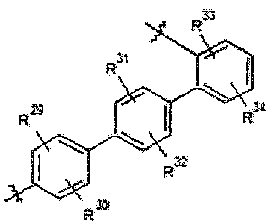
보다 구체적으로, 치환 또는 비치환된 m-터페닐렌기로는 하기와 같은 화학식 S-10, S-11, 및 S-12 등을 예로 들 수 있다.
[화학식 S-10] [화학식 S-11] [화학식 S-12]
[규칙 제91조에 의한 정정 11.07.2013]


보다 구체적으로, 치환 또는 비치환된 o-터페닐렌기로는 하기와 같은 화학식 S-13, S-14, 및 S-15 등을 예로 들 수 있다.
[화학식 S-13] [화학식 S-14] [화학식 S-15]
[규칙 제91조에 의한 정정 11.07.2013]


보다 구체적으로, 치환 또는 비치환된 나프틸렌기로는 하기와 같은 화학식 S-16, S-17, S-18, S-19, S-20, S-21, 및 S-22 등을 예로 들 수 있다.
[화학식 S-16] [화학식 S-17] [화학식 S-18]
[규칙 제91조에 의한 정정 11.07.2013]
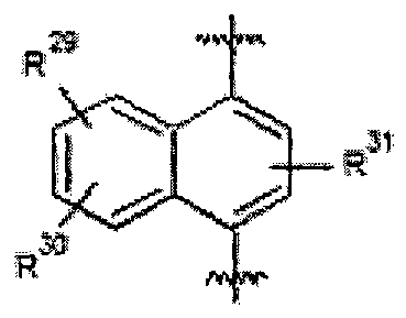


[화학식 S-19] [화학식 S-20] [화학식 S-21]
[규칙 제91조에 의한 정정 11.07.2013]


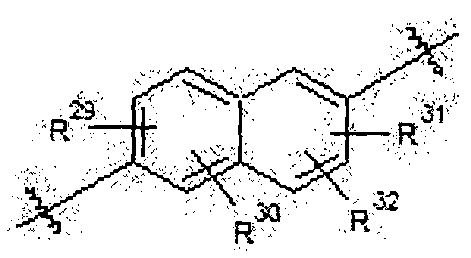
[화학식 S-22]
[규칙 제91조에 의한 정정 11.07.2013]
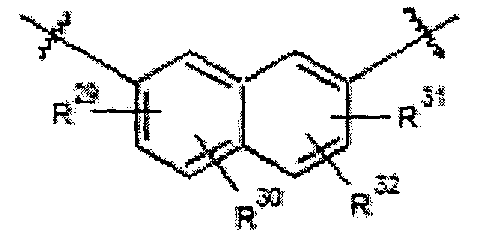
보다 구체적으로, 치환 또는 비치환된 안트라세닐렌기로는 하기와 같은 화학식 S-23, S-24, S-25, S-26, S-27, S-28, 및 S-29 등을 예로 들 수 있다.
[화학식 S-23] [화학식 S-24] [화학식 S-25]
[규칙 제91조에 의한 정정 11.07.2013]


[화학식 S-26] [화학식 S-27] [화학식 S-28]
[규칙 제91조에 의한 정정 11.07.2013]


[화학식 S-29]
[규칙 제91조에 의한 정정 11.07.2013]

보다 구체적으로, 치환 또는 비치환된 페난트릴렌기로는 하기와 같은 화학식 S-30, S-31, S-32, S-33, S-34, S-35, S-36, S-37, S-38, S-39, 및 S-40 등을 예로 들 수 있다.
[화학식 S-30] [화학식 S-31] [화학식 S-32]
[규칙 제91조에 의한 정정 11.07.2013]


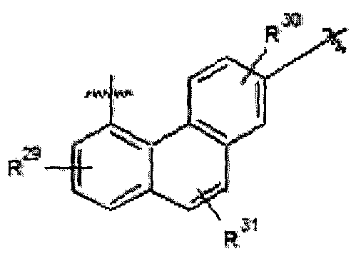
[화학식 S-33] [화학식 S-34] [화학식 S-35]
[규칙 제91조에 의한 정정 11.07.2013]


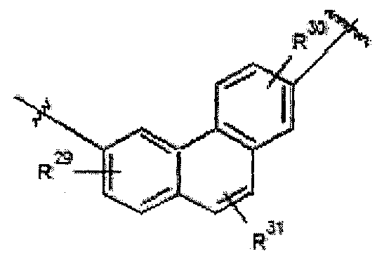
[화학식 S-36] [화학식 S-37] [화학식 S-38]
[규칙 제91조에 의한 정정 11.07.2013]


[화학식 S-39] [화학식 S-40]
[규칙 제91조에 의한 정정 11.07.2013]


보다 구체적으로, 치환 또는 비치환된 피레닐렌기로는 하기와 같은 화학식 S-41, S-42, S-43, S-44, S-45, 및 S-46 등을 예로 들 수 있다.
[화학식 S-41] [화학식 S-42] [화학식 S-43]
[규칙 제91조에 의한 정정 11.07.2013]


[화학식 S-44] [화학식 S-45] [화학식 S-46]
[규칙 제91조에 의한 정정 11.07.2013]


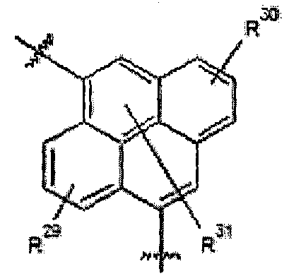
보다 구체적으로, 치환 또는 비치환된 플루오레닐렌기로는 하기와 같은 화학식 S-47, S-48, S-49, S-50, S-51, S-52, S-53, S-54, S-55, 및 S-56 등을 예로 들 수 있다.
[화학식 S-47] [화학식 S-48] [화학식 S-49]
[규칙 제91조에 의한 정정 11.07.2013]


[화학식 S-50] [화학식 S-51] [화학식 S-52]
[규칙 제91조에 의한 정정 11.07.2013]

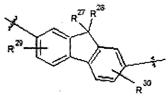

[화학식 S-53] [화학식 S-54] [화학식 S-55]
[규칙 제91조에 의한 정정 11.07.2013]


[화학식 S-56]
[규칙 제91조에 의한 정정 11.07.2013]

상기 L, L1 및 L2의 구체적인 예에서, R27 내지 R34는 서로 독립적으로, 수소, 중수소, 할로겐기, 히드록시기, 아미노기, 치환 또는 비치환된 C1 내지 C30 아민기, 니트로기, 치환 또는 비치환된 C1 내지 C40 실릴기, C1 내지 C30 알킬기, C1 내지 C10 알킬실릴기, C3 내지 C30 시클로알킬기, C6 내지 C30 아릴기, C1 내지 C20 알콕시기, 플루오로기, 트리플루오로메틸기 등의 C1 내지 C10 트리플루오로알킬기 또는 시아노기일 수 있다.
상기 화합물은 입체 장해성을 가지기 때문에 분자 사이의 상호작용이 작아 결정화가 억제될 수 있다. 이로 인해 소자를 제조하는 수율을 향상시킬 수 있다. 또한, 제조된 소자의 수명 특성이 개선될 수 있다.
또한, 상기 화합물은 비교적 분자량이 크기 때문에, 화합물의 증착시의 분해를 억제할 수 있다.
보다 구체적으로, 상기 X1 및 X2은 독립적으로, -O-, -S-, -CRaRb-, 또는 -SiRaRb 일 수 있고, 상기 Ra 및 Rb는 독립적으로 치환 또는 비치환된 C1 내지 C10 알킬기, 또는 치환 또는 비치환된 C6 내지 C30 아릴기일 수 있고, 상기 R1 내지 R4는 독립적으로 수소, 중수소, 치환 또는 비치환된 C1 내지 C10 알킬기, 또는 치환 또는 비치환된 C6 내지 C30 아릴기일 수 있으며, 상기 A는 치환 또는 비치환된 C6 내지 C30 아릴기 또는 치환 또는 비치환된 C2 내지 C30 헤테로아릴기일 수 있다. 이러한 경우, 공액길이가 적절이 조절될 경우 형광 또는 인광 발광 메커니즘을 이용한 발광층 호스트로 사용할 수 있다.
보다 구체적으로 상기 A는 -N(L1
mR')(L2
oR")이고, 상기 R' 또는 R" 중 어느 하나는 하기 화학식 3으로 표시되는 치환기일 수 있다.
[화학식 3]

상기 화학식 3에서, X3 및 X4은 독립적으로, -O-, -S-, -S(O)2-, -CRaRb-, -SiRaRb- 또는 -GeRaRb-이며, 상기 Ra 및 Rb는 독립적으로 수소, 중수소, 치환 또는 비치환된 C1 내지 C10 알킬기, 치환 또는 비치환된 C6 내지 C30 아릴기 또는 치환 또는 비치환된 C2 내지 C30 헤테로아릴기이고, R5 내지 R8는 독립적으로 수소, 중수소, 치환 또는 비치환된 C1 내지 C10 알킬기, 치환 또는 비치환된 C6 내지 C30 아릴기 또는 치환 또는 비치환된 C2 내지 C30 헤테로아릴기이고, 상기 화학식 3의 두 개의 * 중 어느 하나는 상기 -N(L1
mR')(L2
oR")에서 L1 또는 L2와의 결합을 나타낸다.
상기 A가 -N(L1
mR')(L2
oR")이고, 상기 R' 또는 R" 중 어느 하나는 하기 화학식 3으로 표시되는 치환기를 가지는 화합물의 경우, 아민의 세 개의 치환기 중 두 개의 치환기가 상기 화학식 1 또는 3으로 표시되는 치환기인 경우이다.
이러한 경우, 상기 화합물을 정공수송층 또는 정공주입층으로 사용할 수 있다.
보다 구체적으로, 상기 R'는 상기 화학식 3으로 표시되는 치환기이고, 상기 R"는 하기 화학식 4로 표시되는 치환기일 수 있다.
[화학식 4]

상기 화학식 4에서, X5 및 X6은 독립적으로, -O-, -S-, -S(O)2-, -CRaRb-, -SiRaRb- 또는 -GeRaRb-이며, 상기 Ra 및 Rb는 독립적으로 수소, 중수소, 치환 또는 비치환된 C1 내지 C10 알킬기, 치환 또는 비치환된 C6 내지 C30 아릴기 또는 치환 또는 비치환된 C2 내지 C30 헤테로아릴기이고, R9 내지 R12는 독립적으로 수소, 중수소, 치환 또는 비치환된 C1 내지 C10 알킬기, 치환 또는 비치환된 C6 내지 C30 아릴기 또는 치환 또는 비치환된 C2 내지 C30 헤테로아릴기이고, 상기 화학식 4의 두 개의 * 중 어느 하나는 상기 -N(L1
mR')(L2
oR")에서 L1 또는 L2와의 결합을 나타낸다.
상기 A가 -N(L1
mR')(L2
oR")이고, 상기 R'는 상기 화학식 3으로 표시되는 치환기이고, 상기 R"는 하기 화학식 4로 표시되는 치환기인 화합물의 경우, 아민의 세 개의 치환기가 상기 화학식 1, 3 및 4로 표시되는 치환기인 화합물이다.
이러한 경우, 상기 화합물을 정공수송층 또는 정공주입층으로 사용할 수 있다.
보다 구체적으로, 상기 A는 하기 화학식 3으로 표시되는 치환기일 수 있다.
[화학식 3]

상기 화학식 3에서, X3 및 X4은 독립적으로, -O-, -S-, -S(O)2-, -CRaRb-, -SiRaRb- 또는 -GeRaRb-이며, 상기 Ra 및 Rb는 독립적으로 수소, 중수소, 치환 또는 비치환된 C1 내지 C10 알킬기, 치환 또는 비치환된 C6 내지 C30 아릴기 또는 치환 또는 비치환된 C2 내지 C30 헤테로아릴기이고, R5 내지 R8는 독립적으로 수소, 중수소, 치환 또는 비치환된 C1 내지 C10 알킬기, 치환 또는 비치환된 C6 내지 C30 아릴기 또는 치환 또는 비치환된 C2 내지 C30 헤테로아릴기이고, 상기 화학식 3의 두 개의 * 중 어느 하나는 화학식 2의 L과의 결합을 나타낸다.
이러한 경우, 선택적으로 연결기인 L을 사이에 두고 상기 화학식 1과 상기 화학식 3이 결합하는 구조를 가지게 된다. 이러한 경우, 분자 구조를 보다 입체적으로 변화시켜 분자간 중첩에 의한 결정화를 방지할 수 있다. 또한, 상기 화합물에 적절한 헤테로 방향족 치환기가 도입될 경우 분자내 극성 분포에 변화를 주어 인광 발광층 호스트로 사용 시 효율을 증가시킬 수 있다.
상기 R1 내지 R12는 독립적으로 치환 또는 비치환된 페닐기, 치환 또는 비치환된 나프틸기, 치환 또는 비치환된 안트라세닐기, 치환 또는 비치환된 페난트릴기, 치환 또는 비치환된 나프타세닐기, 치환 또는 비치환된 피레닐기, 치환 또는 비치환된 바이페닐일기, 치환 또는 비치환된 p-터페닐기, 치환 또는 비치환된 m-터페닐기, 치환 또는 비치환된 크리세닐기, 치환 또는 비치환된 트리페닐레닐기, 치환 또는 비치환된 페릴레닐기, 치환 또는 비치환된 인데닐기, 치환 또는 비치환된 퓨라닐기, 치환 또는 비치환된 티오페닐기, 치환 또는 비치환된 피롤릴기, 치환 또는 비치환된 피라졸릴기, 치환 또는 비치환된 이미다졸일기, 치환 또는 비치환된 트리아졸일기, 치환 또는 비치환된 옥사졸일기, 치환 또는 비치환된 티아졸일기, 치환 또는 비치환된 옥사디아졸일기, 치환 또는 비치환된 티아디아졸일기, 치환 또는 비치환된 피리딜기, 치환 또는 비치환된 피리미디닐기, 치환 또는 비치환된 피라지닐기, 치환 또는 비치환된 트리아지닐기, 치환 또는 비치환된 벤조퓨라닐기, 치환 또는 비치환된 벤조티오페닐기, 치환 또는 비치환된 벤즈이미다졸일기, 치환 또는 비치환된 인돌일기, 치환 또는 비치환된 퀴놀리닐기, 치환 또는 비치환된 이소퀴놀리닐기, 치환 또는 비치환된 퀴나졸리닐기, 치환 또는 비치환된 퀴녹살리닐기, 치환 또는 비치환된 나프티리디닐기, 치환 또는 비치환된 벤즈옥사진일기, 치환 또는 비치환된 벤즈티아진일기, 치환 또는 비치환된 아크리디닐기, 치환 또는 비치환된 페나진일기, 치환 또는 비치환된 페노티아진일기, 치환 또는 비치환된 페녹사진일기 또는 이들의 조합일 수 있으나, 이에 제한되지는 않는다.
보다 구체적으로, 치환 또는 비치환된 페닐기로는 하기와 같은 화학식 S-57 등을 예로 들 수 있다.
[화학식 S-57]
[규칙 제91조에 의한 정정 11.07.2013]

보다 구체적으로, 치환 또는 비치환된 바이페닐기로는 하기와 같은 화학식 S-58, S-59, 및 S-60 등을 예로 들 수 있다.
[화학식 S-58] [화학식 S-59] [화학식 S-60]
[규칙 제91조에 의한 정정 11.07.2013]
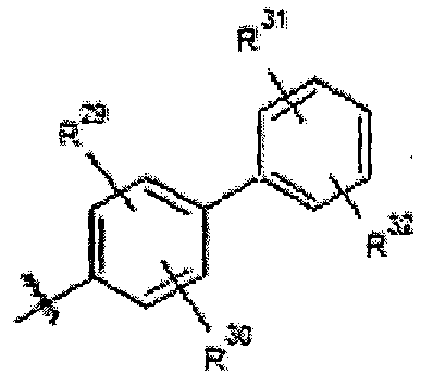
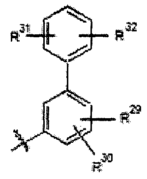
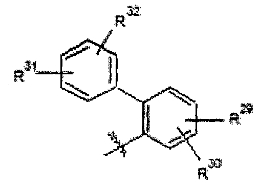
보다 구체적으로, 치환 또는 비치환된 나프틸기로는 하기와 같은 화학식 S-61, 및 S-62 등을 예로 들 수 있다.
[화학식 S-61] [화학식 S-62]
[규칙 제91조에 의한 정정 11.07.2013]

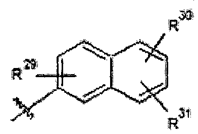
보다 구체적으로, 치환 또는 비치환된 안트라세닐기로는 하기와 같은 화학식 S-63, 및 S-64 등을 예로 들 수 있다.
[화학식 S-63] [화학식 S-64]
[규칙 제91조에 의한 정정 11.07.2013]


보다 구체적으로, 치환 또는 비치환된 페난트레닐기로는 하기와 같은 화학식 S-65, S-66, S-67, S-68, 및 S-69 등을 예로 들 수 있다.
[화학식 S-65] [화학식 S-66] [화학식 S-67]
[규칙 제91조에 의한 정정 11.07.2013]


[화학식 S-68] [화학식 S-69]
[규칙 제91조에 의한 정정 11.07.2013]


보다 구체적으로, 치환 또는 비치환된 트리페닐기로는 하기와 같은 화학식 S-70, 및 S-71 등을 예로 들 수 있다.
[화학식 S-70] [화학식 S-71]
[규칙 제91조에 의한 정정 11.07.2013]


보다 구체적으로, 치환 또는 비치환된 플루오레닐기로는 하기와 같은 화학식 S-72, S-73, S-74, 및 S-75 등을 예로 들 수 있다.
[화학식 S-72] [화학식 S-73] [화학식 S-74]
[규칙 제91조에 의한 정정 11.07.2013]


[화학식 S-75]
[규칙 제91조에 의한 정정 11.07.2013]

이는 상기 화학식 1 내지 4에 모두 적용될 수 있다.
상기 치환기로 인해 상기 유기광전자소자용 화합물은 발광, 정공 또는 전자 특성; 막 안정성; 열적 안정성 및 높은 3중항 여기에너지(T1)를 가질 수 있다.
보다 구체적으로, 상기 유기광전자소자용 화합물은 하기 화학식 A-1 내지 A-183 중 어느 하나로 표시될 수 있으나, 이에 제한되지는 않는다.
[A-1] [A-2] [A-3] [A-4]

[A-5] [A-6] [A-7] [A-8]

[A-9] [A-10] [A-11] [A-12]

[A-13] [A-14] [A-15] [A-16]

[A-17] [A-18] [A-19] [A-20]

[A-21] [A-22] [A-23] [A-24]

[A-25] [A-26] [A-27] [A-28]

[A-29] [A-30] [A-31] [A-32]

[A-33] [A-34] [A-35] [A-36]

[A-37] [A-38] [A-39] [A-40]

[A-41] [A-42] [A-43] [A-44]

[A-45] [A-46] [A-47] [A-48]

[A-49] [A-50] [A-51] [A-52]

[A-53] [A-54] [A-55] [A-56]

[A-57] [A-58] [A-59] [A-60]

[A-61] [A-62] [A-63] [A-64]

[A-65] [A-66] [A-67] [A-68]

[A-69] [A-70] [A-71] [A-72]

[A-73] [A-74] [A-78] [A-79]

[A-80] [A-81] [A-82] [A-83]

[A-84] [A-85] [A-86] [A-87]

[A-88] [A-89] [A-90] [A-91]

[A-92] [A-93] [A-94] [A-95]

[A-96] [A-97] [A-98] [A-99]

[A-100] [A-101] [A-102] [A-103]

[A-104] [A-105] [A-106] [A-107]

[A-108] [A-109] [A-110] [A-111]

[A-112] [A-113] [A-114] [A-115]

[A-116] [A-117] [A-118] [A-119]

[A-120] [A-121] [A-122] [A-123]

[A-124] [A-125] [A-126] [A-127]

[A-128] [A-129] [A-130] [A-131]

[A-132] [A-133] [A-134] [A-135]

[A-136] [A-137] [A-138] [A-139]

[A-140] [A-141] [A-142] [A-143]

[A-144] [A-145] [A-146] [A-147]

[A-148] [A-149] [A-150] [A-151]

[A-152] [A-153] [A-154] [A-155]

[A-156] [A-157] [A-158] [A-159]

[A-160] [A-161] [A-162] [A-163]

[A-164] [A-165] [A-166] [A-167]

[A-168] [A-169] [A-170] [A-171]
[A-172] [A-173] [A-174] [A-175]

[A-176] [A-177] [A-178] [A-179]

[A-180] [A-181] [A-182] [A-183]

보다 구체적으로, 상기 유기광전자소자용 화합물은 하기 화학식 B-1 내지 B-88 중 어느 하나로 표시될 수 있다. 다만, 이에 제한되지는 않는다.
[B-1] [B-2] [B-3] [B-4]

[B-5] [B-6] [B-7] [B-8]

[B-9] [B-10] [B-11] [B-12]

[B-13] [B-14] [B-15] [B-16]

[B-17] [B-18] [B-19] [B-20]

[B-21] [B-22] [B-23] [B-24]

[B-25] [B-26] [B-27] [B-28]

[B-29] [B-30] [B-31] [B-32]

[B-33] [B-34] [B-35] [B-36]

[B-37] [B-38] [B-39] [B-40]

[B-41] [B-42] [B-43] [B-44]

[B-45] [B-46] [B-47] [B-48]

[B-49] [B-50] [B-51] [B-52]

[B-53] [B-54] [B-55] [B-56]

[B-57] [B-58] [B-59] [B-60]

[B-61] [B-62] [B-63] [B-64]

[B-65] [B-66] [B-67] [B-68]

[B-69] [B-70] [B-71] [B-72]

[B-73] [B-74] [B-75] [B-76]

[B-77] [B-78] [B-79] [B-80]

[B-81] [B-82] [B-83] [B-84]

[B-85] [B-86] [B-87] [B-88]

보다 구체적으로, 상기 유기광전자소자용 화합물은 하기 화학식 C-1 내지 C-32 중 어느 하나로 표시될 수 있다. 다만, 이에 제한되는 것은 아니다.
[C-1] [C-2] [C-3] [C-4]

[C-5] [C-6] [C-7] [C-8]

[C-9] [C-10] [C-11] [C-12]

[C-13] [C-14] [C-15] [C-16]

[C-17] [C-18] [C-19] [C-20]

[C-21] [C-22] [C-23] [C-24]

[C-25] [C-26] [C-27] [C-28]

[C-29] [C-30] [C-31] [C-32]

보다 구체적으로, 상기 유기광전자소자용 화합물은 하기 화학식 D-1 내지 D-64 중 어느 하나로 표시될 수 있다. 다만, 이에 제한되는 것은 아니다.
[D-1] [D-2] [D-3] [D-4]

[D-5] [D-6] [D-7] [D-8]

[D-9] [D-10] [D-11] [D-12]

[D-13] [D-14] [D-15] [D-16]

[D-17] [D-18] [D-19] [D-20]

[D-21] [D-22] [D-23] [D-24]

[D-25] [D-26] [D-27] [D-28]

[D-29] [D-30] [D-31] [D-32]

[D-33] [D-34] [D-35] [D-36]

[D-37] [D-38] [D-39] [D-40]

[D-41] [D-42] [D-43] [D-44]

[D-45] [D-46] [D-47] [D-48]

[D-49] [D-50] [D-51] [D-52]

[D-53] [D-54] [D-55] [D-56]

[D-57] [D-58] [D-59] [D-60]

[D-61] [D-62] [D-63] [D-64]

보다 구체적으로, 상기 유기광전자소자용 화합물은 하기 화학식 E-1 내지 E-192 중 어느 하나로 표시될 수 있다. 다만, 이에 제한되는 것은 아니다.
[E-1] [E-2] [E-3] [E-4]

[E-5] [E-6] [E-7] [E-8]

[E-9] [E-10] [E-11] [E-12]

[E-13] [E-14] [E-15] [E-16]

[E-17] [E-18] [E-19] [E-20]
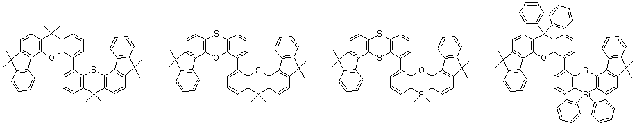
[E-21] [E-22] [E-23] [E-24]

[E-25] [E-26] [E-27] [E-28]

[E-29] [E-30] [E-31]

[E-32] [E-33] [E-34]

[E-35] [E-36] [E-37]

[E-38] [E-39] [E-40]

[E-41] [E-42] [E-43]

[E-44] [E-45] [E-46]

[E-47] [E-48] [E-49]

[E-50] [E-51] [E-52]

[E-53] [E-54] [E-55]

[E-56] [E-57] [E-58]

[E-59] [E-60] [E-61]

[E-62] [E-63] [E-64]

[E-65] [E-66] [E-67]

[E-68] [E-69] [E-70]

[E-71] [E-72] [E-73]

[E-74] [E-75] [E-76] [E-77]

[E-78] [E-79] [E-80] [E-81]

[E-82] [E-83] [E-84] [E-85]

[E-86] [E-87] [E-88] [E-89]

[E-90] [E-91] [E-92]

[E-93] [E-94] [E-95]

[E-96] [E-97] [E-98] [E-99]

[E-100] [E-101] [E-102] [E-103]

[E-104] [E-105] [E-106] [E-107]

[E-108] [E-109] [E-110] [E-111]

[E-112] [E-113] [E-114] [E-115]
[E-116] [E-117] [E-118] [E-119]

[E-120] [E-121] [E-122] [E-123]

[E-124] [E-125] [E-126] [E-127]

[E-128] [E-129] [E-130] [E-131]

[E-132] [E-133] [E-134] [E-135]

[E-136] [E-137] [E-138] [E-139]

[E-140] [E-141] [E-142] [E-143]

[E-144] [E-145] [E-146]

[E-147] [E-148] [E-149]

[E-150] [E-151] [E-152]

[E-153] [E-154] [E-155]

[E-156] [E-157] [E-158]

[E-159] [E-160] [E-161]
*
[E-162] [E-163] [E-164]

[E-165] [E-166] [E-167]

[E-168] [E-169] [E-170]

[E-171] [E-172] [E-173]

[E-174] [E-175] [E-176]

[E-177] [E-178] [E-179] [E-180]

[E-181] [E-182] [E-183] [E-184]

[E-185] [E-186] [E-187] [E-188]

[E-189] [E-190] [E-191] [E-192]

전술한 본 발명의 일 구현예에 따른 화합물이 전자특성, 정공특성 양쪽을 모두 요구하는 경우에는 상기 전자 특성을 가지는 작용기를 도입하는 것이 유기발광소자의 수명 향상 및 구동 전압 감소에 효과적이다.
전술한 본 발명의 일 구현예에 따른 유기광전자소자용 화합물은 최대 발광 파장이 약 320 내지 500 nm 범위를 나타내고, 3중항 여기에너지(T1)가 2.0 eV 이상, 보다 구체적으로 2.0 내지 4.0 eV 범위인 것으로, 높은 3중항 여기 에너지를 가지는 호스트의 전하가 도판트에 잘 전달되어 도판트의 발광효율을 높일 수 있고, 재료의 호모(HOMO)와 루모(LUMO) 에너지 준위를 자유롭게 조절하여 구동전압을 낮출 수 있는 이점이 있기 때문에 호스트 재료 또는 전하수송재료로 매우 유용하게 사용될 수 있다.
뿐만 아니라, 상기 유기광전자소자용 화합물은 광활성 및 전기적인 활성을 갖고 있으므로, 비선형 광학소재, 전극 재료, 변색재료, 광 스위치, 센서, 모듈, 웨이브 가이드, 유기 트렌지스터, 레이저, 광 흡수체, 유전체 및 분리막(membrane) 등의 재료로도 매우 유용하게 적용될 수 있다.
상기와 같은 화합물을 포함하는 유기광전자소자용 화합물은 유리전이온도가 90℃ 이상이며, 열분해온도가 400℃이상으로 열적 안정성이 우수하다. 이로 인해 고효율의 유기광전소자의 구현이 가능하다.
상기와 같은 화합물을 포함하는 유기광전자소자용 화합물은 발광, 또는 전자 주입 및/또는 수송역할을 할 수 있으며, 적절한 도판트와 함께 발광 호스트로서의 역할도 할 수 있다. 즉, 상기 유기광전자소자용 화합물은 인광 또는 형광의 호스트 재료, 청색의 발광도펀트 재료, 또는 전자수송 재료로 사용될 수 있다.
본 발명의 일 구현예에 따른 유기광전자소자용 화합물은 유기박막층에 사용되어 유기광전자소자의 수명 특성, 효율 특성, 전기화학적 안정성 및 열적 안정성을 향상시키며, 구동전압을 낮출 수 있다.
이에 따라 본 발명의 일 구현예는 상기 유기광전자소자용 화합물을 포함하는 유기광전자소자를 제공한다. 이 때, 상기 유기광전자소자라 함은 유기광전소자, 유기발광소자, 유기 태양 전지, 유기 트랜지스터, 유기 감광체 드럼, 유기 메모리 소자 등을 의미한다. 특히, 유기 태양 전지의 경우에는 본 발명의 일 구현예에 따른 유기광전자소자용 화합물이 전극이나 전극 버퍼층에 포함되어 양자 효율을 증가시키며, 유기 트랜지스터의 경우에는 게이트, 소스-드레인 전극 등에서 전극 물질로 사용될 수 있다.
이하에서는 유기발광소자에 대하여 구체적으로 설명한다.
본 발명의 다른 일 구현예는 양극, 음극 및 상기 양극과 음극 사이에 개재되는 적어도 한 층 이상의 유기박막층을 포함하는 유기발광소자에 있어서, 상기 유기박막층 중 적어도 어느 한 층은 본 발명의 일 구현예에 따른 유기광전자소자용 화합물을 포함하는 유기발광소자를 제공한다.
상기 유기광전자소자용 화합물을 포함할 수 있는 유기박막층으로는 발광층, 정공수송층, 정공주입층, 전자수송층, 전자주입층, 정공차단층 및 이들의 조합으로 이루어진 군에서 선택되는 층을 포함할 수 있는 바, 이 중에서 적어도 어느 하나의 층은 본 발명에 따른 유기광전자소자용 화합물을 포함한다. 특히, 정공수송층 또는 정공주입층에 본 발명의 일 구현예에 따른 유기광전자소자용 화합물을 포함할 수 있다. 또한, 상기 유기광전자소자용 화합물이 발광층 내에 포함되는 경우 상기 유기광전자소자용 화합물은 인광 또는 형광호스트로서 포함될 수 있고, 특히, 형광 청색 도펀트 재료로서 포함될 수 있다.
도 1 내지 도 5는 본 발명의 일 구현예에 따른 유기광전자소자용 화합물을 포함하는 유기발광소자의 단면도이다.
도 1 내지 도 5를 참조하면, 본 발명의 일 구현예에 따른 유기발광소자(100, 200, 300, 400 및 500)는 양극(120), 음극(110) 및 이 양극과 음극 사이에 개재된 적어도 1층의 유기박막층(105)을 포함하는 구조를 갖는다.
상기 양극(120)은 양극 물질을 포함하며, 이 양극 물질로는 통상 유기박막층으로 정공주입이 원활할 수 있도록 일함수가 큰 물질이 바람직하다. 상기 양극 물질의 구체적인 예로는 니켈, 백금, 바나듐, 크롬, 구리, 아연, 금과 같은 금속 또는 이들의 합금을 들 수 있고, 아연산화물, 인듐산화물, 인듐주석산화물(ITO), 인듐아연산화물(IZO)과 같은 금속 산화물을 들 수 있고, ZnO와 Al 또는 SnO2와 Sb와 같은 금속과 산화물의 조합을 들 수 있고, 폴리(3-메틸티오펜), 폴리[3,4-(에틸렌-1,2-디옥시)티오펜](polyehtylenedioxythiophene: PEDT), 폴리피롤 및 폴리아닐린과 같은 전도성 고분자 등을 들 수 있으나, 이에 한정되는 것은 아니다. 바람직하게는 상기 양극으로 ITO(indium tin oxide)를 포함하는 투명전극을 사용할 수 있다.
상기 음극(110)은 음극 물질을 포함하여, 이 음극 물질로는 통상 유기박막층으로 전자주입이 용이하도록 일 함수가 작은 물질인 것이 바람직하다. 음극 물질의 구체적인 예로는 마그네슘, 칼슘, 나트륨, 칼륨, 타이타늄, 인듐, 이트륨, 리튬, 가돌리늄, 알루미늄, 은, 주석, 납, 세슘, 바륨 등과 같은 금속 또는 이들의 합금을 들 수 있고, LiF/Al, LiO2/Al,LiF/Ca,LiF/Al및 BaF2/Ca과 같은 다층 구조 물질 등을 들 수 있으나, 이에 한정되는 것은 아니다. 바람직하게는 상기 음극으로 알루미늄 등과 같은 금속전극을 사용할 수 있다.
먼저 도 1을 참조하면, 도 1은 유기박막층(105)으로서 발광층(130)만이 존재하는 유기발광소자(100)를 나타낸 것으로, 상기 유기박막층(105)은 발광층(130)만으로 존재할 수 있다.
도 2를 참조하면, 도 2는 유기박막층(105)으로서 전자수송층을 포함하는 발광층(230)과 정공수송층(140)이 존재하는 2층형 유기발광소자(200)를 나타낸 것으로, 도 2에 나타난 바와 같이, 유기박막층(105)은 발광층(230) 및 정공 수송층(140)을 포함하는 2층형일 수 있다. 이 경우 발광층(130)은 전자 수송층의 기능을 하며, 정공 수송층(140)은 ITO와 같은 투명전극과의 접합성 및 정공수송성을 향상시키는 기능을 한다.
도 3을 참조하면, 도 3은 유기박막층(105)으로서 전자수송층(150), 발광층(130) 및 정공수송층(140)이 존재하는 3층형 유기발광소자(300)로서, 상기 유기박막층(105)에서 발광층(130)은 독립된 형태로 되어 있고, 전자수송성이나 정공수송성이 우수한 막(전자수송층(150) 및 정공수송층(140))을 별도의 층으로 쌓은 형태를 나타내고 있다.
도 4를 참조하면, 도 4는 유기박막층(105)으로서 전자주입층(160), 발광층(130), 정공수송층(140) 및 정공주입층(170)이 존재하는 4층형 유기발광소자(400)로서, 상기 정공주입층(170)은 양극으로 사용되는 ITO와의 접합성을 향상시킬 수 있다.
도 5를 참조하면, 도 5는 유기박막층(105)으로서 전자주입층(160), 전자수송층(150), 발광층(130), 정공수송층(140) 및 정공주입층(170)과 같은 각기 다른 기능을 하는 5개의 층이 존재하는 5층형 유기발광소자(500)를 나타내고 있으며, 상기 유기발광소자(500)는 전자주입층(160)을 별도로 형성하여 저전압화에 효과적이다.
상기 도 1 내지 도 5에서 상기 유기박막층(105)을 이루는 전자 수송층(150), 전자 주입층(160), 발광층(130, 230), 정공 수송층(140), 정공 주입층(170) 및 이들의 조합으로 이루어진 군에서 선택되는 어느 하나는 상기 유기광전자소자용 화합물을 포함한다. 이 때 상기 유기광전자소자용 화합물은 상기 전자 수송층(150) 또는 전자주입층(160)을 포함하는 전자수송층(150)에 사용될 수 있으며, 그중에서도 전자수송층에 포함될 경우 정공 차단층(도시하지 않음)을 별도로 형성할 필요가 없어 보다 단순화된 구조의 유기발광소자를 제공할 수 있어 바람직하다.
또한, 상기 유기광전자소자용 화합물이 발광층(130, 230) 내에 포함되는 경우 상기 유기광전자소자용 화합물은 인광 또는 형광호스트로서 포함될 수 있으며, 또는 형광 청색 도펀트로서 포함될 수 있다.
상기에서 설명한 유기발광소자는, 기판에 양극을 형성한 후, 진공증착법(evaporation), 스퍼터링(sputtering), 플라즈마 도금 및 이온도금과 같은 건식성막법; 또는 스핀코팅(spin coating), 침지법(dipping), 유동코팅법(flow coating)과 같은 습식성막법 등으로 유기박막층을 형성한 후, 그 위에 음극을 형성하여 제조할 수 있다.
본 발명의 또 다른 일 구현예에 따르면, 상기 유기발광소자를 포함하는 표시장치를 제공한다.
이하에서는 본 발명의 구체적인 실시예들을 제시한다. 다만, 하기에 기재된 실시예들은 본 발명을 구체적으로 예시하거나 설명하기 위한 것에 불과하며, 이로서 본 발명이 제한되어서는 아니된다.
(유기광전소자용 화합물의 제조)
중간체의 합성
중간체 M-1의 합성
[반응식 1]

티안스렌-1-보로닉 산(tianthrene-1-boronic acid) 20g(76.88mmol), 메틸-2-브로모-5-클로로벤조에이트 21.1g(84.57mmol) 및 테트라키스트리페닐포스핀팔라듐 0.89g(0.769mmol)을 플라스크에 넣고 질소 분위기 하에 테트라하이드로퓨란 257mL에 용해 시킨 후 포타슘 카보네이트 17g (115.3mmol)을 녹인 수용액 128ml를 첨가 시킨 후 8시간 동안 70℃에서 환류 교반 하였다. 반응 종료 후 에틸아세테이트로 추출 한 후 추출액을 마그네슘설페이트로 건조, 여과하고 여과액을 감압 농축하였다. 생성물을 n-헥산/에틸아세테이트(9:1 부피비)으로 실리카 겔 컬럼 크로마토 그래피로 정제하여 목적 화합물인 중간체 M-1을 26.9g(수율 91%)을 수득 하였다.
LC-Mass (이론치: 384.00g/mol, 측정치: M+1 = 385.11g/mol)
중간체 M-2의 합성
[반응식 2]

진공 하에서 가열 건조한 3구 둥근 바닥 플라스크에 질소 분위기 하에서 중간체 M-1 25g(64.95mmol)을 넣고 무수 테트라하이드로퓨란 325mL를 가하여 용해시킨 후 -10℃로 냉각 및 교반 하였다.
여기에 3.0M 메틸마그네슘브로마이드 54mL(디에틸에테르 내, 162.4mmol) 을 30분간 천천히 가한다. 반응액을 상온으로 승온하고 질소 분위기 하에 12시간 교반 하였다. 반응액을 0℃로 냉각한 후 여기에 암모늄클로라이드 10.4g (194.85mmol)을 증류수 100mL에 녹인 수용액을 천천히 가한다. 반응액을 증류수와 디에틸에테르로 추출하고 유기층 용액을 마그네슘설페이트로 건조, 여과하고 여과액을 감압 농축하였다. 건조된 잔사를 3구 둥근 바닥 플라스크에 넣은 후 질소분위기 하에서 무수 디클로로메탄 325mL를 가하여 용해시킨 후 0℃로 냉각 및 교반 하였다. 여기에 보론트리플루오라이드 디에틸 이써레이트 4mL (32.5mmol)을 10분간 천천히 가하고 실온으로 승온한 후 12시간 동안 교반한다. 반응이 종료되면 중탄산나트륨 수용액을 0℃에서 천천히 가한후 30분간 교반한다. 반응액을 디클로로메탄/증류수로 추출한 추출액을 마그네슘설페이트로 건조, 여과하고 여과액을 감압 농축하였다. 생성물을 n-헥산/디클로로메탄(9:1 부피비)으로 실리카 겔 컬럼 크로마토 그래피로 정제하여 목적 화합물인 중간체 M-2를 15.5g(수율 65%)을 수득 하였다.
LC-Mass (이론치: 366.03g/mol, 측정치: M+1 = 367.14g/mol)
중간체 M-3의 합성
[반응식 3]

4-페녹사티인일보론산(4-Phenoxathiinylboronic acid) 18.8g(76.88mmol), 메틸-2-브로모-5-클로로벤조에이트 21.1g(84.57mmol) 및 테트라키스트리페닐포스핀팔라듐 0.89g(0.769mmol)을 플라스크에 넣고 질소 분위기 하에 테트라하이드로퓨란 257mL에 용해 시킨 후 포타슘 카보네이트 17g (115.3mmol)을 녹인 수용액 128ml를 첨가 시킨 후 8시간 동안 70℃에서 환류 교반 하였다. 반응 종료 후 에틸아세테이트로 추출 한 후 추출액을 마그네슘설페이트로 건조, 여과하고 여과액을 감압 농축하였다. 생성물을 n-헥산/에틸아세테이트(9:1 부피비)으로 실리카 겔 컬럼 크로마토 그래피로 정제하여 목적 화합물인 중간체 M-3를 26.1g(수율 92%)을 수득 하였다.
LC-Mass (이론치: 368.03g/mol, 측정치: M+1 = 369.21g/mol)
중간체 M-4의 합성
[반응식 4]

진공 하에서 가열 건조한 3구 둥근 바닥 플라스크에 질소 분위기 하에서 중간체 M-3 24g(64.95mmol)을 넣고 무수 테트라하이드로퓨란 325mL를 가하여 용해시킨 후 -10℃로 냉각 및 교반 하였다.
여기에 3.0M 메틸마그네슘브로마이드 54mL(디에틸에테르 내, 162.4mmol) 을 30분간 천천히 가한다. 반응액을 상온으로 승온하고 질소 분위기 하에 12시간 교반 하였다. 반응액을 0℃로 냉각한 후 여기에 암모늄클로라이드 10.4g (194.85mmol)을 증류수 100mL에 녹인 수용액을 천천히 가한다. 반응액을 증류수와 디에틸에테르로 추출하고 유기층 용액을 마그네슘설페이트로 건조, 여과하고 여과액을 감압 농축하였다. 건조된 잔사를 3구 둥근 바닥 플라스크에 넣은 후 질소분위기 하에서 무수 디클로로메탄 325mL를 가하여 용해시킨 후 0℃로 냉각 및 교반 하였다. 여기에 보론트리플루오라이드 디에틸 이써레이트 4mL (32.5mmol)을 10분간 천천히 가하고 실온으로 승온한 후 12시간 동안 교반한다. 반응이 종료되면 중탄산나트륨 수용액을 0℃에서 천천히 가한후 30분간 교반한다. 반응액을 디클로로메탄/증류수로 추출한 추출액을 마그네슘설페이트로 건조, 여과하고 여과액을 감압 농축하였다. 생성물을 n-헥산/디클로로메탄(9:1 부피비)으로 실리카 겔 컬럼 크로마토 그래피로 정제하여 목적 화합물인 중간체 M-2를 15.5g(수율 68%)을 수득 하였다.
LC-Mass (이론치: 350.05g/mol, 측정치: M+1 = 351.18g/mol)
중간체 M-5의 합성
[반응식 5]

진공 하에서 가열 건조한 2구 둥근 바닥 플라스크에 질소 분위기 하에서 9,9-디메틸잔텐 30g(142.7mmol)을 넣고 무수 테트라하이드로퓨란 476mL를 가하여 용해시킨 후 -40℃로 냉각 및 교반하였다.
여기에 2.5M n-부틸리튬 57mL(헥산 내, 142.7mmol)을 천천히 가한 후 N,N,N',N'-테트라메틸에틸렌디아민 16.5g(142.7mmol)을 가한다. 반응액을 상온으로 승온하고 질소 분위기 하에 8시간 교반 하였다. 반응액을 -78℃로 냉각한 후 여기에 무수 테트라하이드로퓨란 10mL에 녹인 트리메틸보레이트 10.9g(157mmol)을 천천히 가한 후 상온에서 8시간 교반 하였다. 반응액을 0℃로 냉각하고 여기에 2N HCl 수용액 234mL를 가하고 1시간 동안 상온에서 교반 하였다. 반응 종료 후 용액을 증류수와 디에틸에테르로 추출하고 유기층 용액을 마그네슘설페이트로 건조, 여과하고 여과액을 감압 농축하였다. 반응액을 아세톤에 녹인 후 n-헥산으로 재결정하여 목적화합물인 중간체 M-5를 흰색고체로 23.6g(수율 65%)을 수득하였다.
GC-Mass (이론치: 254.11g/mol, 측정치: M+1 = 255.42g/mol)
중간체 M-6의 합성
[반응식 6]

중간체 M-5 19.5g(76.88mmol), 메틸-2-브로모-5-클로로벤조에이트 21.1g(84.57mmol) 및 테트라키스트리페닐포스핀팔라듐 0.89g(0.769mmol)을 플라스크에 넣고 질소 분위기 하에 테트라하이드로퓨란 257mL에 용해 시킨 후 포타슘 카보네이트 17g (115.3mmol)을 녹인 수용액 128ml를 첨가 시킨 후 8시간 동안 70℃에서 환류 교반 하였다. 반응 종료 후 에틸아세테이트로 추출 한 후 추출액을 마그네슘설페이트로 건조, 여과하고 여과액을 감압 농축하였다. 생성물을 n-헥산/에틸아세테이트(9:1 부피비)으로 실리카 겔 컬럼 크로마토 그래피로 정제하여 목적 화합물인 중간체 M-6을 26.2g(수율 90%)을 수득 하였다.
LC-Mass (이론치: 378.10g/mol, 측정치: M+1 = 379.31g/mol)
중간체 M-7의 합성
[반응식 7]

진공 하에서 가열 건조한 3구 둥근 바닥 플라스크에 질소 분위기 하에서 중간체 M-6 24.6g(64.95mmol)을 넣고 무수 테트라하이드로퓨란 325mL를 가하여 용해시킨 후 -10℃로 냉각 및 교반 하였다.
여기에 3.0M 메틸마그네슘브로마이드 54mL(디에틸에테르 내, 162.4mmol) 을 30분간 천천히 가한다. 반응액을 상온으로 승온하고 질소 분위기 하에 12시간 교반 하였다. 반응액을 0℃로 냉각한 후 여기에 암모늄클로라이드 10.4g (194.85mmol)을 증류수 100mL에 녹인 수용액을 천천히 가한다. 반응액을 증류수와 디에틸에테르로 추출하고 유기층 용액을 마그네슘설페이트로 건조, 여과하고 여과액을 감압 농축하였다. 건조된 잔사를 3구 둥근 바닥 플라스크에 넣은 후 질소분위기 하에서 무수 디클로로메탄 325mL를 가하여 용해시킨 후 0℃로 냉각 및 교반 하였다. 여기에 보론트리플루오라이드 디에틸 이써레이트 4mL (32.5mmol)을 10분간 천천히 가하고 실온으로 승온한 후 12시간 동안 교반한다. 반응이 종료되면 중탄산나트륨 수용액을 0℃에서 천천히 가한후 30분간 교반한다. 반응액을 디클로로메탄/증류수로 추출한 추출액을 마그네슘설페이트로 건조, 여과하고 여과액을 감압 농축하였다. 생성물을 n-헥산/디클로로메탄(9:1 부피비)으로 실리카 겔 컬럼 크로마토 그래피로 정제하여 목적 화합물인 중간체 M-7을 15.7g(수율 67%)을 수득 하였다.
LC-Mass (이론치: 360.13g/mol, 측정치: M+1 = 361.26g/mol)
중간체 M-8의 합성
[반응식 8]

진공 하에서 가열 건조한 2구 둥근 바닥 플라스크에 질소 분위기 하에서 디페닐에테르 60g(352.6mmol)을 넣고 무수 테트라하이드로퓨란 352mL를 가하여 용해시킨 후 0℃로 냉각 및 교반하였다.
여기에 2.5M n-부틸리튬 310mL(헥산 내, 776mmol)을 천천히 가한 후 N,N,N',N'-테트라메틸에틸렌디아민 90.2g(776mmol)을 가한다. 반응액을 상온으로 승온하고 질소 분위기 하에 16시간 교반 하였다. 반응액을 0℃로 냉각한 후 여기에 무수 디에틸에테르 60mL에 녹인 디메틸디클로로실란 45.6g(352.6mmol)을 천천히 가한 후 상온에서 16시간 교반 하였다. 반응액을 0℃로 냉각하고 여기에 증류수 240mL를 가하고 30분간 상온에서 교반 하였다. 반응 종료 후 용액을 증류수와 디에틸에테르로 추출하고 유기층 용액을 마그네슘설페이트로 건조, 여과하고 여과액을 감압 농축하였다. 생성물을 메탄올로 재결정하여 목적화합물인 중간체 M-8을 흰색 고체로 35.2g(수율 44%)을 수득하였다.
GC-Mass (이론치: 226.08g/mol, 측정치: M+1 = 227.27g/mol)
중간체 M-9의 합성
[반응식 9]

진공 하에서 가열 건조한 2구 둥근 바닥 플라스크에 질소 분위기 하에서 중간체 M-8 32.3g(142.7mmol)을 넣고 무수 테트라하이드로퓨란 476mL를 가하여 용해시킨 후 -40℃로 냉각 및 교반하였다.
여기에 2.5M n-부틸리튬 57mL(헥산 내, 142.7mmol)을 천천히 가한 후 N,N,N',N'-테트라메틸에틸렌디아민 16.5g(142.7mmol)을 가한다. 반응액을 상온으로 승온하고 질소 분위기 하에 8시간 교반 하였다. 반응액을 -78℃로 냉각한 후 여기에 무수 테트라하이드로퓨란 10mL에 녹인 트리메틸보레이트 10.9g(157mmol)을 천천히 가한 후 상온에서 8시간 교반 하였다. 반응액을 0℃로 냉각하고 여기에 2N HCl 수용액 234mL를 가하고 1시간 동안 상온에서 교반 하였다. 반응 종료 후 용액을 증류수와 디에틸에테르로 추출하고 유기층 용액을 마그네슘설페이트로 건조, 여과하고 여과액을 감압 농축하였다. 반응액을 아세톤에 녹인 후 n-헥산으로 재결정하여 목적화합물인 중간체 M-9를 흰색 고체로 22.7g(수율 59%)을 수득하였다.
GC-Mass (이론치: 270.09g/mol, 측정치: M+1 = 271.35g/mol)
중간체 M-10의 합성
[반응식 10]

중간체 M-9 20.8g(76.88mmol), 메틸-2-브로모-5-클로로벤조에이트 21.1g(84.57mmol) 및 테트라키스트리페닐포스핀팔라듐 0.89g(0.769mmol)을 플라스크에 넣고 질소 분위기 하에 테트라하이드로퓨란 257mL에 용해 시킨 후 포타슘 카보네이트 17g (115.3mmol)을 녹인 수용액 128ml를 첨가 시킨 후 8시간 동안 70℃에서 환류 교반 하였다. 반응 종료 후 에틸아세테이트로 추출 한 후 추출액을 마그네슘설페이트로 건조, 여과하고 여과액을 감압 농축하였다. 생성물을 n-헥산/에틸아세테이트(9:1 부피비)으로 실리카 겔 컬럼 크로마토 그래피로 정제하여 목적 화합물인 중간체 M-10을 27g(수율 89%)을 수득 하였다.
LC-Mass (이론치: 394.08g/mol, 측정치: M+1 = 395.29g/mol)
중간체 M-11의 합성
[반응식 11]

진공 하에서 가열 건조한 3구 둥근 바닥 플라스크에 질소 분위기 하에서 중간체 M-10 25.7g(64.95mmol)을 넣고 무수 테트라하이드로퓨란 325mL를 가하여 용해시킨 후 -10℃로 냉각 및 교반 하였다.
여기에 3.0M 메틸마그네슘브로마이드 54mL(디에틸에테르 내, 162.4mmol) 을 30분간 천천히 가한다. 반응액을 상온으로 승온하고 질소 분위기 하에 12시간 교반 하였다. 반응액을 0℃로 냉각한 후 여기에 암모늄클로라이드 10.4g (194.85mmol)을 증류수 100mL에 녹인 수용액을 천천히 가한다. 반응액을 증류수와 디에틸에테르로 추출하고 유기층 용액을 마그네슘설페이트로 건조, 여과하고 여과액을 감압 농축하였다. 건조된 잔사를 3구 둥근 바닥 플라스크에 넣은 후 질소분위기 하에서 무수 디클로로메탄 325mL를 가하여 용해시킨 후 0℃로 냉각 및 교반 하였다. 여기에 보론트리플루오라이드 디에틸 이써레이트 4mL (32.5mmol)을 10분간 천천히 가하고 실온으로 승온한 후 12시간 동안 교반한다. 반응이 종료되면 중탄산나트륨 수용액을 0℃에서 천천히 가한후 30분간 교반한다. 반응액을 디클로로메탄/증류수로 추출한 추출액을 마그네슘설페이트로 건조, 여과하고 여과액을 감압 농축하였다. 생성물을 n-헥산/디클로로메탄(9:1 부피비)으로 실리카 겔 컬럼 크로마토 그래피로 정제하여 목적 화합물인 중간체 M-11을 15.9g(수율 65%)을 수득 하였다.
LC-Mass (이론치: 376.11g/mol, 측정치: M+1 = 377.25g/mol)
중간체 M-12의 합성
[반응식 12]

진공 하에서 가열 건조한 2구 둥근 바닥 플라스크에 질소 분위기 하에서 티옥산텐-9-온(tioxanthene-9-one) 40g(188.4mmol)을 넣고 무수 톨루엔 377mL를 가하여 용해시킨 후 0℃로 냉각 및 교반하였다.
여기에 2.0M 트리메틸알루미늄 188mL(톨루엔 내, 377mmol)을 천천히 가한 후 반응액을 상온으로 승온 하고 질소 분위기 하에 12시간 교반 하였다.
6N HCl 수용액 188mL와 얼음 181g을 섞은 슬러리에 반응액을 천천히 가하고 30분간 상온에서 교반 하였다. 반응 종료 후 용액을 증류수와 톨루엔으로 추출하고 유기층 용액을 마그네슘설페이트로 건조, 여과하고 여과액을 감압 농축하였다. 생성물을 n-헥산으로 실리카 겔 컬럼 크로마토그래피로 정제하여 목적 화합물인 중간체 M-12를 34.1g(수율 80%)을 수득 하였다.
LC-Mass (이론치: 226.08g/mol, 측정치: M+1 = 227.35g/mol)
중간체 M-13의 합성
[반응식 13]

진공 하에서 가열 건조한 2구 둥근 바닥 플라스크에 질소 분위기 하에서 중간체 M-12 32.3g(142.7mmol)을 넣고 무수 테트라하이드로퓨란 476mL를 가하여 용해시킨 후 -40℃로 냉각 및 교반하였다.
여기에 2.5M n-부틸리튬 57mL(헥산 내, 142.7mmol)을 천천히 가한 후 N,N,N',N'-테트라메틸에틸렌디아민 16.5g(142.7mmol)을 가한다. 반응액을 상온으로 승온하고 질소 분위기 하에 8시간 교반 하였다. 반응액을 -78℃로 냉각한 후 여기에 무수 테트라하이드로퓨란 10mL에 녹인 트리메틸보레이트 10.9g(157mmol)을 천천히 가한 후 상온에서 8시간 교반 하였다. 반응액을 0℃로 냉각하고 여기에 2N HCl 수용액 234mL를 가하고 1시간 동안 상온에서 교반 하였다. 반응 종료 후 용액을 증류수와 디에틸에테르로 추출하고 유기층 용액을 마그네슘설페이트로 건조, 여과하고 여과액을 감압 농축하였다. 반응액을 아세톤에 녹인 후 n-헥산으로 재결정하여 목적화합물인 중간체 M-13을 흰색 고체로 23.5g(수율 61%)을 수득하였다.
GC-Mass (이론치: 270.09g/mol, 측정치: M+1 = 271.27g/mol)
중간체 M-14의 합성
[반응식 14]

중간체 M-13 20.8g(76.88mmol), 메틸-2-브로모벤조에이트 18.2g (84.57mmol) 및 테트라키스트리페닐포스핀팔라듐 0.89g(0.769mmol)을 플라스크에 넣고 질소 분위기 하에 테트라하이드로퓨란 257mL에 용해 시킨 후 포타슘 카보네이트 17g (115.3mmol)을 녹인 수용액 128ml를 첨가 시킨 후 8시간 동안 70℃에서 환류 교반 하였다. 반응 종료 후 에틸아세테이트로 추출 한 후 추출액을 마그네슘설페이트로 건조, 여과하고 여과액을 감압 농축하였다. 생성물을 n-헥산/에틸아세테이트(9:1 부피비)으로 실리카 겔 컬럼 크로마토 그래피로 정제하여 목적 화합물인 중간체 M-14를 25.5g(수율 92%)을 수득 하였다.
LC-Mass (이론치: 360.12g/mol, 측정치: M+1 = 361.25g/mol)
중간체 M-15의 합성
[반응식 15]

진공 하에서 가열 건조한 3구 둥근 바닥 플라스크에 질소 분위기 하에서 중간체 M-14 23.4g(64.95mmol)을 넣고 무수 테트라하이드로퓨란 325mL를 가하여 용해시킨 후 -10℃로 냉각 및 교반 하였다.
여기에 3.0M 메틸마그네슘브로마이드 54mL(디에틸에테르 내, 162.4mmol) 을 30분간 천천히 가한다. 반응액을 상온으로 승온하고 질소 분위기 하에 12시간 교반 하였다. 반응액을 0℃로 냉각한 후 여기에 암모늄클로라이드 10.4g (194.85mmol)을 증류수 100mL에 녹인 수용액을 천천히 가한다. 반응액을 증류수와 디에틸에테르로 추출하고 유기층 용액을 마그네슘설페이트로 건조, 여과하고 여과액을 감압 농축하였다. 건조된 잔사를 3구 둥근 바닥 플라스크에 넣은 후 질소분위기 하에서 무수 디클로로메탄 325mL를 가하여 용해시킨 후 0℃로 냉각 및 교반 하였다. 여기에 보론트리플루오라이드 디에틸 이써레이트 4mL (32.5mmol)을 10분간 천천히 가하고 실온으로 승온한 후 12시간 동안 교반한다. 반응이 종료되면 중탄산나트륨 수용액을 0℃에서 천천히 가한후 30분간 교반한다. 반응액을 디클로로메탄/증류수로 추출한 추출액을 마그네슘설페이트로 건조, 여과하고 여과액을 감압 농축하였다. 생성물을 n-헥산/디클로로메탄(9:1 부피비)으로 실리카 겔 컬럼 크로마토 그래피로 정제하여 목적 화합물인 중간체 M-15를 14.7g(수율 66%)을 수득 하였다.
LC-Mass (이론치: 342.14g/mol, 측정치: M+1 = 343.19g/mol)
중간체 M-16의 합성
[반응식 16]

진공 하에서 가열 건조한 2구 둥근 바닥 플라스크에 질소 분위기 하에서 중간체 M-19 24.5g(71.4mmol)을 넣고 무수 테트라하이드로퓨란 238mL를 가하여 용해시킨 후 -40℃로 냉각 및 교반하였다.
여기에 2.5M n-부틸리튬 28.6mL(헥산 내, 71.4mmol)을 천천히 가한 후 N,N,N',N'-테트라메틸에틸렌디아민 8.3g(71.4mmol)을 가한다. 반응액을 상온으로 승온하고 질소 분위기 하에 8시간 교반 하였다. 반응액을 -78℃로 냉각한 후 여기에 무수 테트라하이드로퓨란 10mL에 녹인 트리메틸보레이트 8.9g(85.7mmol)을 천천히 가한 후 상온에서 8시간 교반 하였다. 반응액을 0℃로 냉각하고 여기에 2N HCl 수용액 117mL를 가하고 1시간 동안 상온에서 교반 하였다. 반응 종료 후 용액을 증류수와 디에틸에테르로 추출하고 유기층 용액을 마그네슘설페이트로 건조, 여과하고 여과액을 감압 농축하였다. 반응액을 아세톤에 녹인 후 n-헥산으로 재결정하여 목적화합물인 중간체 M-20을 흰색 고체로 17.9g(수율 65%)을 수득하였다.
GC-Mass (이론치: 386.15g/mol, 측정치: M+1 = 387.19g/mol)
중간체 M-17의 합성
[반응식 17]

중간체 M-16 18g(46.6mmol), 1-브로모-4-클로로벤젠 8.9g(46.6mmol) 및 테트라키스트리페닐포스핀팔라듐 0.54g(0.466mmol)을 플라스크에 넣고 질소 분위기 하에 톨루엔 233mL에 용해 시킨 후 포타슘 카보네이트 10.3g (69.9mmol)을 녹인 수용액 80ml를 첨가 시키고 8시간 동안 100℃에서 환류 교반 하였다. 반응 종료 후 에틸아세테이트로 추출 한 후 추출액을 마그네슘설페이트로 건조, 여과하고 여과액을 감압 농축하였다. 생성물을 n-헥산/디클로로메탄(9:1 부피비)으로 실리카 겔 컬럼 크로마토 그래피로 정제하여 목적 화합물인 중간체 M-17을 19.2g(수율 91%)을 수득 하였다.
LC-Mass (이론치: 452.14g/mol, 측정치: M+1 = 453.23g/mol)
중간체 M-18의 합성
[반응식 18]

중간체 M-9 20.8g(76.88mmol), 메틸-2-브로모벤조에이트 18.2g (84.57mmol) 및 테트라키스트리페닐포스핀팔라듐 0.89g(0.769mmol)을 플라스크에 넣고 질소 분위기 하에 테트라하이드로퓨란 257mL에 용해 시킨 후 포타슘 카보네이트 17g (115.3mmol)을 녹인 수용액 128ml를 첨가 시킨 후 8시간 동안 70℃에서 환류 교반 하였다. 반응 종료 후 에틸아세테이트로 추출 한 후 추출액을 마그네슘설페이트로 건조, 여과하고 여과액을 감압 농축하였다. 생성물을 n-헥산/에틸아세테이트(9:1 부피비)으로 실리카 겔 컬럼 크로마토 그래피로 정제하여 목적 화합물인 중간체 M-18을 24.9g(수율 90%)을 수득 하였다.
LC-Mass (이론치: 360.12g/mol, 측정치: M+1 = 361.33g/mol)
중간체 M-19의 합성
[반응식 19]

진공 하에서 가열 건조한 3구 둥근 바닥 플라스크에 질소 분위기 하에서 중간체 M-18 23.4g(64.95mmol)을 넣고 무수 테트라하이드로퓨란 325mL를 가하여 용해시킨 후 -10℃로 냉각 및 교반 하였다.
여기에 3.0M 메틸마그네슘브로마이드 54mL(디에틸에테르 내, 162.4mmol) 을 30분간 천천히 가한다. 반응액을 상온으로 승온하고 질소 분위기 하에 12시간 교반 하였다. 반응액을 0℃로 냉각한 후 여기에 암모늄클로라이드 10.4g (194.85mmol)을 증류수 100mL에 녹인 수용액을 천천히 가한다. 반응액을 증류수와 디에틸에테르로 추출하고 유기층 용액을 마그네슘설페이트로 건조, 여과하고 여과액을 감압 농축하였다. 건조된 잔사를 3구 둥근 바닥 플라스크에 넣은 후 질소분위기 하에서 무수 디클로로메탄 325mL를 가하여 용해시킨 후 0℃로 냉각 및 교반 하였다. 여기에 보론트리플루오라이드 디에틸 이써레이트 4mL (32.5mmol)을 10분간 천천히 가하고 실온으로 승온한 후 12시간 동안 교반한다. 반응이 종료되면 중탄산나트륨 수용액을 0℃에서 천천히 가한후 30분간 교반한다. 반응액을 디클로로메탄/증류수로 추출한 추출액을 마그네슘설페이트로 건조, 여과하고 여과액을 감압 농축하였다. 생성물을 n-헥산/디클로로메탄(9:1 부피비)으로 실리카 겔 컬럼 크로마토 그래피로 정제하여 목적 화합물인 중간체 M-19를 15.1g(수율 68%)을 수득 하였다.
LC-Mass (이론치: 342.14g/mol, 측정치: M+1 = 343.22g/mol)
중간체 M-20의 합성
[반응식 20]

진공 하에서 가열 건조한 2구 둥근 바닥 플라스크에 질소 분위기 하에서 중간체 M-19 24.5g(71.4mmol)을 넣고 무수 테트라하이드로퓨란 238mL를 가하여 용해시킨 후 -40℃로 냉각 및 교반하였다.
여기에 2.5M n-부틸리튬 28.6mL(헥산 내, 71.4mmol)을 천천히 가한 후 N,N,N',N'-테트라메틸에틸렌디아민 8.3g(71.4mmol)을 가한다. 반응액을 상온으로 승온하고 질소 분위기 하에 8시간 교반 하였다. 반응액을 -78℃로 냉각한 후 여기에 무수 테트라하이드로퓨란 10mL에 녹인 트리메틸보레이트 8.9g(85.7mmol)을 천천히 가한 후 상온에서 8시간 교반 하였다. 반응액을 0℃로 냉각하고 여기에 2N HCl 수용액 117mL를 가하고 1시간 동안 상온에서 교반 하였다. 반응 종료 후 용액을 증류수와 디에틸에테르로 추출하고 유기층 용액을 마그네슘설페이트로 건조, 여과하고 여과액을 감압 농축하였다. 반응액을 아세톤에 녹인 후 n-헥산으로 재결정하여 목적화합물인 중간체 M-20을 흰색 고체로 18.5g(수율 67%)을 수득하였다.
GC-Mass (이론치: 386.15g/mol, 측정치: M+1 = 387.24g/mol)
중간체 M-21의 합성
[반응식 21]

중간체 M-20 18g(46.6mmol), 1-브로모-4-클로로벤젠 8.9g(46.6mmol) 및 테트라키스트리페닐포스핀팔라듐 0.54g(0.466mmol)을 플라스크에 넣고 질소 분위기 하에 톨루엔 233mL에 용해 시킨 후 포타슘 카보네이트 10.3g (69.9mmol)을 녹인 수용액 80ml를 첨가 시키고 8시간 동안 100℃에서 환류 교반 하였다. 반응 종료 후 에틸아세테이트로 추출 한 후 추출액을 마그네슘설페이트로 건조, 여과하고 여과액을 감압 농축하였다. 생성물을 n-헥산/디클로로메탄(9:1 부피비)으로 실리카 겔 컬럼 크로마토 그래피로 정제하여 목적 화합물인 중간체 M-17을 19.6g(수율 93%)을 수득 하였다.
LC-Mass (이론치: 452.14g/mol, 측정치: M+1 = 453.28g/mol)
중간체 M-22의 합성
[반응식 22]

4-페녹사티일보로닉 산(4-Phenoxathiinylboronic acid) 18.8g(76.88mmol), 메틸-2-브로모벤조에이트 18.2g (84.57mmol) 및 테트라키스트리페닐포스핀팔라듐 0.89g(0.769mmol)을 플라스크에 넣고 질소 분위기 하에 테트라하이드로퓨란 257mL에 용해 시킨 후 포타슘 카보네이트 17g (115.3mmol)을 녹인 수용액 128ml를 첨가 시킨 후 8시간 동안 70℃에서 환류 교반 하였다. 반응 종료 후 에틸아세테이트로 추출 한 후 추출액을 마그네슘설페이트로 건조, 여과하고 여과액을 감압 농축하였다. 생성물을 n-헥산/에틸아세테이트(9:1 부피비)으로 실리카 겔 컬럼 크로마토 그래피로 정제하여 목적 화합물인 중간체 M-22를 23.4g(수율 91%)을 수득 하였다.
LC-Mass (이론치: 334.39g/mol, 측정치: M+1 = 335.28g/mol)
중간체 M-23의 합성
[반응식 23]

진공 하에서 가열 건조한 3구 둥근 바닥 플라스크에 질소 분위기 하에서 중간체 M-22 21.7g(64.95mmol)을 넣고 무수 테트라하이드로퓨란 325mL를 가하여 용해시킨 후 -10℃로 냉각 및 교반 하였다.
여기에 3.0M 메틸마그네슘브로마이드 54mL(디에틸에테르 내, 162.4mmol) 을 30분간 천천히 가한다. 반응액을 상온으로 승온하고 질소 분위기 하에 12시간 교반 하였다. 반응액을 0℃로 냉각한 후 여기에 암모늄클로라이드 10.4g (194.85mmol)을 증류수 100mL에 녹인 수용액을 천천히 가한다. 반응액을 증류수와 디에틸에테르로 추출하고 유기층 용액을 마그네슘설페이트로 건조, 여과하고 여과액을 감압 농축하였다. 건조된 잔사를 3구 둥근 바닥 플라스크에 넣은 후 질소분위기 하에서 무수 디클로로메탄 325mL를 가하여 용해시킨 후 0℃로 냉각 및 교반 하였다. 여기에 보론트리플루오라이드 디에틸 이써레이트 4mL (32.5mmol)을 10분간 천천히 가하고 실온으로 승온한 후 12시간 동안 교반한다. 반응이 종료되면 중탄산나트륨 수용액을 0℃에서 천천히 가한후 30분간 교반한다. 반응액을 디클로로메탄/증류수로 추출한 추출액을 마그네슘설페이트로 건조, 여과하고 여과액을 감압 농축하였다. 생성물을 n-헥산/디클로로메탄(9:1 부피비)으로 실리카 겔 컬럼 크로마토 그래피로 정제하여 목적 화합물인 중간체 M-23을 13.2g(수율 64%)을 수득 하였다.
LC-Mass (이론치: 316.42g/mol, 측정치: M+1 = 317.55g/mol)
중간체 M-24의 합성
[반응식 24]

진공 하에서 가열 건조한 2구 둥근 바닥 플라스크에 질소 분위기 하에서 중간체 M-23 13g(41.08mmol)을 넣고 무수 디에틸에테르 410mL를 가하여 용해시킨 후 0℃로 냉각 및 교반하였다.
여기에 2.5M n-부틸리튬 16.4mL(헥산 내, 41.08mmol)을 가한 후 반응액을 승온하여 질소 분위기 하에 24시간 동안 환류 교반 하였다. 반응액을 -40℃로 냉각한 후 여기에 무수 디에틸에테르 10mL에 녹인 트리메틸보레이트 4.7g(45.2mmol)을 천천히 가한 후 상온에서 12시간 교반 하였다. 반응액을 0℃로 냉각하고 여기에 2N HCl 수용액 68mL를 가하고 1시간 동안 상온에서 교반 하였다. 반응 종료 후 용액을 증류수와 디에틸에테르로 추출하고 유기층 용액을 마그네슘설페이트로 건조, 여과하고 여과액을 감압 농축하였다. 반응액을 아세톤에 녹인 후 n-헥산으로 재결정하여 목적화합물인 중간체 M-24를 흰색 고체로 7.7g(수율 52%)을 수득하였다.
GC-Mass (이론치: 360.10g/mol, 측정치: M+1 = 361.28g/mol)
중간체 M-25의 합성
[반응식 25]

중간체 M-24 7g(19.43mmol), 1,4-디브로모나프탈렌 8.3g(29.15mmol) 및 테트라키스트리페닐포스핀팔라듐 0.23g(0.194mmol)을 플라스크에 넣고 질소 분위기 하에 톨루엔 190mL에 용해 시킨 후 포타슘 카보네이트 4.3g (29.14mmol)을 녹인 수용액 60ml를 첨가 시키고 8시간 동안 100℃에서 환류 교반 하였다. 반응 종료 후 에틸아세테이트로 추출 한 후 추출액을 마그네슘설페이트로 건조, 여과하고 여과액을 감압 농축하였다. 생성물을 n-헥산/디클로로메탄(9:1 부피비)으로 실리카 겔 컬럼 크로마토 그래피로 정제하여 목적 화합물인 중간체 M-25을 7.9g(수율 78%)을 수득 하였다.
LC-Mass (이론치: 520.05g/mol, 측정치: M+1 = 521.16g/mol)
중간체 M-26의 합성
[반응식 26]

중간체 M-13 20.8g(76.88mmol), 메틸-2-브로모-5-클로로벤조에이트 21.1g(84.57mmol) 및 테트라키스트리페닐포스핀팔라듐 0.89g(0.769mmol)을 플라스크에 넣고 질소 분위기 하에 테트라하이드로퓨란 257mL에 용해 시킨 후 포타슘 카보네이트 17g (115.3mmol)을 녹인 수용액 128ml를 첨가 시킨 후 8시간 동안 70℃에서 환류 교반 하였다. 반응 종료 후 에틸아세테이트로 추출 한 후 추출액을 마그네슘설페이트로 건조, 여과하고 여과액을 감압 농축하였다. 생성물을 n-헥산/에틸아세테이트(9:1 부피비)으로 실리카 겔 컬럼 크로마토 그래피로 정제하여 목적 화합물인 중간체 M-26을 27.3g(수율 90%)을 수득 하였다.
LC-Mass (이론치: 394.08g/mol, 측정치: M+1 = 395.16g/mol)
중간체 M-27의 합성
[반응식 27]

진공 하에서 가열 건조한 3구 둥근 바닥 플라스크에 질소 분위기 하에서 중간체 M-26 25.6g(64.95mmol)을 넣고 무수 테트라하이드로퓨란 325mL를 가하여 용해시킨 후 -10℃로 냉각 및 교반 하였다.
여기에 3.0M 메틸마그네슘브로마이드 54mL(디에틸에테르 내, 162.4mmol) 을 30분간 천천히 가한다. 반응액을 상온으로 승온하고 질소 분위기 하에 12시간 교반 하였다. 반응액을 0℃로 냉각한 후 여기에 암모늄클로라이드 10.4g (194.85mmol)을 증류수 100mL에 녹인 수용액을 천천히 가한다. 반응액을 증류수와 디에틸에테르로 추출하고 유기층 용액을 마그네슘설페이트로 건조, 여과하고 여과액을 감압 농축하였다. 건조된 잔사를 3구 둥근 바닥 플라스크에 넣은 후 질소분위기 하에서 무수 디클로로메탄 325mL를 가하여 용해시킨 후 0℃로 냉각 및 교반 하였다. 여기에 보론트리플루오라이드 디에틸 이써레이트 4mL (32.5mmol)을 10분간 천천히 가하고 실온으로 승온한 후 12시간 동안 교반한다. 반응이 종료되면 중탄산나트륨 수용액을 0℃에서 천천히 가한후 30분간 교반한다. 반응액을 디클로로메탄/증류수로 추출한 추출액을 마그네슘설페이트로 건조, 여과하고 여과액을 감압 농축하였다. 생성물을 n-헥산/디클로로메탄(9:1 부피비)으로 실리카 겔 컬럼 크로마토 그래피로 정제하여 목적 화합물인 중간체 M-27을 15.4g(수율 63%)을 수득 하였다.
LC-Mass (이론치: 376.11g/mol, 측정치: M+1 = 377.23g/mol)
중간체 M-28의 합성
[반응식 28]

티안스렌-1-보로닉 산(tianthrene-1-boronic acid) 20g(76.88mmol), 메틸-2-브로모-4-클로로벤조에이트 21.1g(84.57mmol) 및 테트라키스트리페닐포스핀팔라듐 0.89g(0.769mmol)을 플라스크에 넣고 질소 분위기 하에 테트라하이드로퓨란 257mL에 용해 시킨 후 포타슘 카보네이트 17g (115.3mmol)을 녹인 수용액 128ml를 첨가 시킨 후 8시간 동안 70℃에서 환류 교반 하였다. 반응 종료 후 에틸아세테이트로 추출 한 후 추출액을 마그네슘설페이트로 건조, 여과하고 여과액을 감압 농축하였다. 생성물을 n-헥산/에틸아세테이트(9:1 부피비)으로 실리카 겔 컬럼 크로마토 그래피로 정제하여 목적 화합물인 중간체 M-28을 27.2g(수율 92%)을 수득 하였다.
LC-Mass (이론치: 384.00g/mol, 측정치: M+1 = 385.21g/mol)
중간체 M-29의 합성
[반응식 29]

진공 하에서 가열 건조한 3구 둥근 바닥 플라스크에 질소 분위기 하에서 중간체 M-28 25g(64.95mmol)을 넣고 무수 테트라하이드로퓨란 325mL를 가하여 용해시킨 후 -10℃로 냉각 및 교반 하였다.
여기에 3.0M 메틸마그네슘브로마이드 54mL(디에틸에테르 내, 162.4mmol) 을 30분간 천천히 가한다. 반응액을 상온으로 승온하고 질소 분위기 하에 12시간 교반 하였다. 반응액을 0℃로 냉각한 후 여기에 암모늄클로라이드 10.4g (194.85mmol)을 증류수 100mL에 녹인 수용액을 천천히 가한다. 반응액을 증류수와 디에틸에테르로 추출하고 유기층 용액을 마그네슘설페이트로 건조, 여과하고 여과액을 감압 농축하였다. 건조된 잔사를 3구 둥근 바닥 플라스크에 넣은 후 질소분위기 하에서 무수 디클로로메탄 325mL를 가하여 용해시킨 후 0℃로 냉각 및 교반 하였다. 여기에 보론트리플루오라이드 디에틸 이써레이트 4mL (32.5mmol)을 10분간 천천히 가하고 실온으로 승온한 후 12시간 동안 교반한다. 반응이 종료되면 중탄산나트륨 수용액을 0℃에서 천천히 가한후 30분간 교반한다. 반응액을 디클로로메탄/증류수로 추출한 추출액을 마그네슘설페이트로 건조, 여과하고 여과액을 감압 농축하였다. 생성물을 n-헥산/디클로로메탄(9:1 부피비)으로 실리카 겔 컬럼 크로마토 그래피로 정제하여 목적 화합물인 중간체 M-29를 16.7g(수율 70%)을 수득 하였다.
LC-Mass (이론치: 366.03g/mol, 측정치: M+1 = 367.14g/mol)
실시예 1: 화학식 A-2로 표시되는 화합물의 제조
[반응식 28]

중간체 M-2 11.2g(30.59mmol)와 비스-바이페닐-4-일-아민(bis-biphenyl-4-yl-amine) 9.8g(30.59mmol), 소디윰 t-부톡사이드 3.8g(39.8mmol)를 둥근 바닥 플라스크에 넣고 톨루엔 200mL를 가한 후 트리-tert-부틸포스핀 0.19g(0.92mmol)과 Pd(dba)2 0.18g(0.31mmol)을 넣고 질소 분위기 하에서 12시간 동안 100℃에서 교반 시킨다. 반응 종료 후 톨루엔과 증류수로 추출 후 유기층을 마그네슘설페이트로 건조, 여과하고 여과액을 감압 농축하였다. 생성물을 n-헥산/디클로로메탄(7:3 부피비)으로 실리카 겔 컬럼 크로마토그래피로 정제하여 목적 화합물인 A-2를 18.1g(수율 91%)을 수득 하였다.
LC-Mass (이론치: 651.21g/mol, 측정치: M+1 = 652.32g/mol)
실시예 2: 화학식 A-3으로 표시되는 화합물의 제조
[반응식 29]

중간체 M-4 10.7g(30.59mmol)와 비스-바이페닐-4-일-아민(bis-biphenyl-4-yl-amine) 9.8g(30.59mmol), 소디윰 t-부톡사이드 3.8g(39.8mmol)를 둥근 바닥 플라스크에 넣고 톨루엔 200mL를 가한 후 트리-tert-부틸포스핀 0.19g(0.92mmol)과 Pd(dba)2 0.18g(0.31mmol)을 넣고 질소 분위기 하에서 12시간 동안 100℃에서 교반 시킨다. 반응 종료 후 톨루엔과 증류수로 추출 후 유기층을 마그네슘설페이트로 건조, 여과하고 여과액을 감압 농축하였다. 생성물을 n-헥산/디클로로메탄(7:3 부피비)으로 실리카 겔 컬럼 크로마토그래피로 정제하여 목적 화합물인 A-3를 18.1g(수율 93%)을 수득 하였다.
LC-Mass (이론치: 635.23g/mol, 측정치: M+1 = 636.51g/mol)
실시예 3: 화학식 A-37로 표시되는 화합물의 제조
[반응식 30]

중간체 M-7 11.04g(30.59mmol)과 바이페닐-4-일-페닐-아민(biphenyl-4-yl-phenyl-amine) 7.5g (30.59mmol), 소디윰 t-부톡사이드 3.8g(39.8mmol)를 둥근 바닥 플라스크에 넣고 톨루엔 200mL를 가한 후 트리-tert-부틸포스핀 0.19g(0.92mmol)과 Pd(dba)20.18g(0.31mmol)을 넣고 질소 분위기 하에서 12시간 동안 100℃에서 교반 시킨다. 반응 종료 후 톨루엔과 증류수로 추출 후 유기층을 마그네슘설페이트로 건조, 여과하고 여과액을 감압 농축하였다. 생성물을 n-헥산/디클로로메탄(7:3 부피비)으로 실리카 겔 컬럼 크로마토그래피로 정제하여 목적 화합물인 A-37을 15.7g(수율 90%)을 수득 하였다.
LC-Mass (이론치: 569.27g/mol, 측정치: M+1 = 570.36g/mol)
실시예 4: 화학식 A-39로 표시되는 화합물의 제조
[반응식 31]

중간체 M-11 11.5g(30.59mmol)과 바이페닐-4-일-나프탈렌-1-일-아민(biphenyl-4-yl-naphthalen-1-yl-amine) 9.0g (30.59mmol), 소디윰 t-부톡사이드 3.8g(39.8mmol)를 둥근 바닥 플라스크에 넣고 톨루엔 200mL를 가한 후 트리-tert-부틸포스핀 0.19g(0.92mmol)과 Pd(dba)2 0.18g(0.31mmol)을 넣고 질소 분위기 하에서 12시간 동안 100℃에서 교반 시킨다. 반응 종료 후 톨루엔과 증류수로 추출 후 유기층을 마그네슘설페이트로 건조, 여과하고 여과액을 감압 농축하였다. 생성물을 n-헥산/디클로로메탄(7:3 부피비)으로 실리카 겔 컬럼 크로마토그래피로 정제하여 목적 화합물인 A-39를 17.9g(수율 92%)을 수득 하였다.
LC-Mass (이론치: 635.26g/mol, 측정치: M+1 = 636.31g/mol)
실시예 5: 화학식 B-10으로 표시되는 화합물의 제조
[반응식 32]

중간체 M-17 13.9g(30.59mmol)과 바이페닐-4-일-나프탈렌-1-일-아민(biphenyl-4-yl-naphthalen-1-yl-amine) 9.0g (30.59mmol), 소디윰 t-부톡사이드 3.8g(39.8mmol)를 둥근 바닥 플라스크에 넣고 톨루엔 200mL를 가한 후 트리-tert-부틸포스핀 0.19g(0.92mmol)과 Pd(dba)2 0.18g(0.31mmol)을 넣고 질소 분위기 하에서 12시간 동안 100℃에서 교반 시킨다. 반응 종료 후 톨루엔과 증류수로 추출 후 유기층을 마그네슘설페이트로 건조, 여과하고 여과액을 감압 농축하였다. 생성물을 n-헥산/디클로로메탄(7:3 부피비)으로 실리카 겔 컬럼 크로마토그래피로 정제하여 목적 화합물인 A-39를 19.4g(수율 89%)을 수득 하였다.
LC-Mass (이론치: 711.30g/mol, 측정치: M+1 = 712.28g/mol)
실시예 6: 화학식 B-11로 표시되는 화합물의 제조
[반응식 33]

중간체 M-21 13.9g(30.59mmol)와 비스-바이페닐-4-일-아민(bis-biphenyl-4-yl-amine) 9.8g(30.59mmol), 소디윰 t-부톡사이드 3.8g(39.8mmol)를 둥근 바닥 플라스크에 넣고 톨루엔 200mL를 가한 후 트리-tert-부틸포스핀 0.19g(0.92mmol)과 Pd(dba)2 0.18g(0.31mmol)을 넣고 질소 분위기 하에서 12시간 동안 100℃에서 교반 시킨다. 반응 종료 후 톨루엔과 증류수로 추출 후 유기층을 마그네슘설페이트로 건조, 여과하고 여과액을 감압 농축하였다. 생성물을 n-헥산/디클로로메탄(7:3 부피비)으로 실리카 겔 컬럼 크로마토그래피로 정제하여 목적 화합물인 B-11을 20.3g(수율 90%)을 수득 하였다.
LC-Mass (이론치: 737.31g/mol, 측정치: M+1 = 738.28g/mol)
실시예 7: 화학식 B-19로 표시되는 화합물의 제조
[반응식 34]

중간체 M-25 16g(30.59mmol)와 비스-바이페닐-4-일-아민(bis-biphenyl-4-yl-amine) 9.8g(30.59mmol), 소디윰 t-부톡사이드 3.8g(39.8mmol)를 둥근 바닥 플라스크에 넣고 톨루엔 200mL를 가한 후 트리-tert-부틸포스핀 0.19g(0.92mmol)과 Pd(dba)2 0.18g(0.31mmol)을 넣고 질소 분위기 하에서 12시간 동안 100℃에서 교반 시킨다. 반응 종료 후 톨루엔과 증류수로 추출 후 유기층을 마그네슘설페이트로 건조, 여과하고 여과액을 감압 농축하였다. 생성물을 n-헥산/디클로로메탄(7:3 부피비)으로 실리카 겔 컬럼 크로마토그래피로 정제하여 목적 화합물인 B-19를 20.5g(수율 88%)을 수득 하였다.
LC-Mass (이론치: 761.28g/mol, 측정치: M+1 = 762.31g/mol)
실시예 8: 화학식 D-5로 표시되는 화합물의 제조
[반응식 35]

중간체 M-27 11.5g(30.59mmol)와 4-아미노비페닐 2.6g(15.3mmol), 소디윰 t-부톡사이드 3.8g(39.8mmol)를 둥근 바닥 플라스크에 넣고 톨루엔 200mL를 가한 후 트리-tert-부틸포스핀 0.19g(0.92mmol)과 Pd(dba)2 0.18g(0.31mmol)을 넣고 질소 분위기 하에서 12시간 동안 100℃에서 교반 시킨다. 반응 종료 후 톨루엔과 증류수로 추출 후 유기층을 마그네슘설페이트로 건조, 여과하고 여과액을 감압 농축하였다. 생성물을 n-헥산/디클로로메탄(7:3 부피비)으로 실리카 겔 컬럼 크로마토그래피로 정제하여 목적 화합물인 D-5를 11.2g(수율 86%)을 수득 하였다.
LC-Mass (이론치: 849.35g/mol, 측정치: M+1 = 850.16g/mol)
실시예 9: 화학식 D-20로 표시되는 화합물의 제조
[반응식 36]

중간체 M-7 11.04g(30.59mmol)와 1-아미노나프탈렌 2.2g(15.3mmol), 소디윰 t-부톡사이드 3.8g(39.8mmol)를 둥근 바닥 플라스크에 넣고 톨루엔 200mL를 가한 후 트리-tert-부틸포스핀 0.19g(0.92mmol)과 Pd(dba)20.18g(0.31mmol)을 넣고 질소 분위기 하에서 12시간 동안 100℃에서 교반 시킨다. 반응 종료 후 톨루엔과 증류수로 추출 후 유기층을 마그네슘설페이트로 건조, 여과하고 여과액을 감압 농축하였다. 생성물을 n-헥산/디클로로메탄(7:3 부피비)으로 실리카 겔 컬럼 크로마토그래피로 정제하여 목적 화합물인 D-20을 11g (수율 90%)을 수득 하였다.
LC-Mass (이론치: 791.38g/mol, 측정치: M+1 = 792.42g/mol)
실시예 10: 화학식 A-165로 표시되는 화합물의 제조
[반응식 37]

중간체 M-29 11.2g(30.59mmol)와 비스-바이페닐-4-일-아민(bis-biphenyl-4-yl-amine) 9.8g(30.59mmol), 소디윰 t-부톡사이드 3.8g(39.8mmol)를 둥근 바닥 플라스크에 넣고 톨루엔 200mL를 가한 후 트리-tert-부틸포스핀 0.19g(0.92mmol)과 Pd(dba)2 0.18g(0.31mmol)을 넣고 질소 분위기 하에서 12시간 동안 100℃에서 교반 시킨다. 반응 종료 후 톨루엔과 증류수로 추출 후 유기층을 마그네슘설페이트로 건조, 여과하고 여과액을 감압 농축하였다. 생성물을 n-헥산/디클로로메탄(7:3 부피비)으로 실리카 겔 컬럼 크로마토그래피로 정제하여 목적 화합물인 A-165를 18.5g(수율 93%)을 수득 하였다.
LC-Mass (이론치: 651.21g/mol, 측정치: M+1 = 652.32g/mol)
(유기발광소자의 제조)
실시예 11
ITO (Indium tin oxide)가 1500Å의 두께가 박막 코팅된 유리 기판을 증류수 초음파로 세척하였다. 증류수 세척이 끝나면 이소프로필 알코올, 아세톤, 메탄올 등의 용제로 초음파 세척을 하고 건조시킨 후 플라즈마 세정기로 이송 시킨 다음 산소 플라즈마를 이용하여 상기 기판을 5분간 세정 한 후 진공 층착기로 기판을 이송하였다. 이렇게 준비된 ITO 투명 전극을 양극으로 사용하여 ITO 기판 상부에 4,4'-bis[N-[4-{N,N-bis(3-methylphenyl)amino}-phenyl]-N-phenylamino]biphenyl (DNTPD)를 진공 증착하여 600Å두께의 정공 주입층을 형성하였다. 이어서 실시예 1에서 제조된 화합물을 사용하여 진공 증착으로 300Å 두께의 정공 수송층을 형성하였다. 상기 정공 수송층 상부에 9,10-디-(2-나프틸)안트라센(9,10-di-(2-naphthyl)anthracene, ADN)을 호스트로 사용하고 도판트로 2,5,8,11-테트라(터셔리-부틸)페릴렌(2,5,8,11-tetra(tert-butyl)perylene, TBPe)를 3중량%로 도핑하여 진공 증착으로 250Å 두께의 발광층을 형성하였다.
그 후 상기 발광층 상부에 Alq3를 진공 증착하여 250Å 두께의 전자수송층을 형성하였다. 상기 전자수송층 상부에 LiF 10Å과 Al 1000Å을 순차적으로 진공 증착하여 음극을 형성함으로써 유기발광소자를 제조하였다.
상기 유기발광소자는 5층의 유기박막층을 가지는 구조로 되어 있으며, 구체적으로
Al(1000Å)/LiF(10Å)/Alq3(250Å)/EML[ADN:TBPe=97:3](250Å)/HTL(300Å)/DNTPD (600Å)/ITO(1500Å)의 구조로 제작하였다.
실시예 12
상기 실시예 10에서, 실시예 1 대신 실시예 2를 사용한 점을 제외하고는 동일한 방법으로 유기발광소자를 제조하였다.
실시예 13
상기 실시예 10에서, 실시예 1 대신 실시예 3을 사용한 점을 제외하고는 동일한 방법으로 유기발광소자를 제조하였다.
실시예 14
상기 실시예 10에서, 실시예 1 대신 실시예 4를 사용한 점을 제외하고는 동일한 방법으로 유기발광소자를 제조하였다.
실시예 15
상기 실시예 10에서, 실시예 1 대신 실시예 5를 사용한 점을 제외하고는 동일한 방법으로 유기발광소자를 제조하였다.
실시예 16
상기 실시예 10에서, 실시예 1 대신 실시예 6을 사용한 점을 제외하고는 동일한 방법으로 유기발광소자를 제조하였다.
실시예 17
상기 실시예 10에서, 실시예 1 대신 실시예 7을 사용한 점을 제외하고는 동일한 방법으로 유기발광소자를 제조하였다.
실시예 18
상기 실시예 10에서, 실시예 1 대신 실시예 8을 사용한 점을 제외하고는 동일한 방법으로 유기발광소자를 제조하였다.
실시예 19
상기 실시예 10에서, 실시예 1 대신 실시예 9를 사용한 점을 제외하고는 동일한 방법으로 유기발광소자를 제조하였다.
비교예 1
상기 실시예 11에서, 실시예 1 대신 NPB를 사용한 점을 제외하고는 동일한 방법으로 유기발광소자를 제조하였다. 상기 NPB의 구조는 하기에 기재되어 있다.
상기 유기발광소자 제작에 사용된 DNTPD, ADN, TBPe, NPB, Alq3의 구조는 아래와 같다.
[DNTPD] [ADN] [TBPe]

[NPB] [Alq3]

(유기발광소자의 성능 측정)
상기 실시예 11 내지 19과 비교예 1 에서 제조된 각각의 유기발광소자에 대하여 전압에 따른 전류밀도 변화, 휘도변화 및 발광효율을 측정하였다. 구체적인 측정방법은 하기와 같고, 그 결과는 하기 표 1에 나타내었다.
(1) 전압변화에 따른 전류밀도의 변화 측정
제조된 유기발광소자에 대해, 전압을 0 V 부터 10 V까지 상승시키면서 전류-전압계(Keithley 2400)를 이용하여 단위소자에 흐르는 전류값을 측정하고, 측정된 전류값을 면적으로 나누어 결과를 얻었다.
(2) 전압변화에 따른 휘도변화 측정
제조된 유기발광소자에 대해, 전압을 0 V 부터 10 V까지 상승시키면서 휘도계(Minolta Cs-1000A)를 이용하여 그 때의 휘도를 측정하여 결과를 얻었다.
(3) 발광효율 측정
상기(1) 및 (2)로부터 측정된 휘도와 전류밀도 및 전압을 이용하여 동일 전류밀도(10 mA/cm2)의 전류 효율(cd/A) 을 계산하였다.
표 1
| 소 자 | 정공 수송층에 사용한 화합물 | 전압(V) | 색(EL color) | 효율(cd/A) | 반감 수명(h) at 1000cd/m2 |
| 실시예 11 | A-2 | 6.3 | Blue | 6.3 | 1,610 |
| 실시예 12 | A-3 | 6.2 | Blue | 6.5 | 1,720 |
| 실시예 13 | A-37 | 6.7 | Blue | 6.3 | 1,590 |
| 실시예 14 | A-39 | 6.5 | Blue | 6.4 | 1,690 |
| 실시예 15 | B-10 | 6.8 | Blue | 5.9 | 1,390 |
| 실시예 16 | B-11 | 6.8 | Blue | 6.1 | 1,460 |
| 실시예 17 | B-19 | 6.7 | Blue | 6.1 | 1,430 |
| 실시예 18 | D-5 | 6.7 | Blue | 6.2 | 1,280 |
| 실시예 19 | D-20 | 6.6 | Blue | 6.4 | 1,310 |
| 비교예 1 | NPB | 7.1 | Blue | 4.9 | 1,250 |
전류밀도: 10mA/cm2
상기 표 1의 결과에 따르면 상기 실시예 11 내지 19은 유기발광소자용 정공수송층으로 사용될 때, 유기발광소자의 구동전압을 낮추고, 휘도와 효율을 향상시킴을 알 수 있다.
또한, 상기 실시예 11 내지 실시예 19의 반감 수명은 상기 비교예 1 보다 크게 향상되었으며, 특히 상기 실시예 12의 반감수명은 1,720 시간(h)으로 비교예 1의 반감수명인 1,250 시간보다 약 37% 이상 향상된 것을 알 수 있다.
실제 소자의 상업화 측면에서 소자의 수명은 제품화의 가장 큰 문제 중 하나임을 고려할 때 상기 실시예들의 결과는 소자를 제품화하여 상업화하기에 충분한 것으로 판단된다.
본 발명은 상기 실시예들에 한정되는 것이 아니라 서로 다른 다양한 형태로 제조될 수 있으며, 본 발명이 속하는 기술분야에서 통상의 지식을 가진 자는 본 발명의 기술적 사상이나 필수적인 특징을 변경하지 않고서 다른 구체적인 형태로 실시될 수 있다는 것을 이해할 수 있을 것이다. 그러므로 이상에서 기술한 실시예들은 모든 면에서 예시적인 것이며 한정적이 아닌 것으로 이해해야만 한다.
Claims (18)
- 하기 화학식 1 및 2의 조합으로 표시되는 유기광전자소자용 화합물:[화학식 1] [화학식 2]

 상기 화학식 1 및 2에서,X1 및 X2은 독립적으로, -O-, -S-, -S(O)2-, -CRaRb-, -SiRaRb- 또는 -GeRaRb-이며, 상기 Ra 및 Rb는 독립적으로 수소, 중수소, 치환 또는 비치환된 C1 내지 C10 알킬기, 치환 또는 비치환된 C6 내지 C30 아릴기 또는 치환 또는 비치환된 C2 내지 C30 헤테로아릴기이고,R1 내지 R4는 독립적으로 수소, 중수소, 치환 또는 비치환된 C1 내지 C10 알킬기, 치환 또는 비치환된 C6 내지 C30 아릴기 또는 치환 또는 비치환된 C2 내지 C30 헤테로아릴기이고,A는 치환 또는 비치환된 C6 내지 C30 아릴기, 치환 또는 비치환된 C2 내지 C30 헤테로아릴기 또는 -N(L1 mR')(L2 oR")이며, 상기 R' 및 R"는 독립적으로 수소, 중수소, 치환 또는 비치환된 C1 내지 C10 알킬기, 치환 또는 비치환된 C6 내지 C30 아릴기 또는 치환 또는 비치환된 C2 내지 C30 헤테로아릴기이고,L은 -SiR'R"-, 치환 또는 비치환된 C2 내지 C10 알케닐렌기, 치환 또는 비치환된 C2 내지 C10 알키닐렌기, 치환 또는 비치환된 C6 내지 C30 아릴렌기 또는 치환 또는 비치환된 C2 내지 C30 헤테로아릴렌기이며, 상기 R' 및 R"는 독립적으로 수소, 중수소, 치환 또는 비치환된 C1 내지 C10 알킬기, 치환 또는 비치환된 C6 내지 C30 아릴기 또는 치환 또는 비치환된 C2 내지 C30 헤테로아릴기이고,L1 및 L2는 독립적으로 치환 또는 비치환된 C2 내지 C10 알케닐렌기, 치환 또는 비치환된 C2 내지 C10 알키닐렌기, 치환 또는 비치환된 C6 내지 C30 아릴렌기 또는 치환 또는 비치환된 C2 내지 C30 헤테로아릴렌기이고,n, m 및 o는 독립적으로 0 내지 3의 정수 중 어느 하나이고,화학식 2의 *는 화학식 1의 두 개의 * 중 어느 하나의 결합 위치를 나타낸다.
 - 제1항에 있어서,상기 X1 및 X2은 독립적으로, -O-, -S-, -CRaRb-, 또는 -SiRaRb 이고,상기 Ra 및 Rb는 독립적으로 치환 또는 비치환된 C1 내지 C10 알킬기, 또는 치환 또는 비치환된 C6 내지 C30 아릴기인 유기광전자소자용 화합물.
- 제1항에 있어서,상기 R1 내지 R4는 독립적으로 수소, 중수소, 치환 또는 비치환된 C1 내지 C10 알킬기, 또는 치환 또는 비치환된 C6 내지 C30 아릴기인 유기광전자소자용 화합물.
- 제1항에 있어서,상기 A는 치환 또는 비치환된 C6 내지 C30 아릴기 또는 치환 또는 비치환된 C2 내지 C30 헤테로아릴기인 것인 유기광전자소자용 화합물.
- 제1항에 있어서,상기 A는 -N(L1 mR')(L2 oR")이고,상기 R' 또는 R" 중 어느 하나는 하기 화학식 3으로 표시되는 치환기인 것인 유기광전자소자용 화합물:[화학식 3]
 상기 화학식 3에서,X3 및 X4은 독립적으로, -O-, -S-, -S(O)2-, -CRaRb-, -SiRaRb- 또는 -GeRaRb-이며, 상기 Ra 및 Rb는 독립적으로 수소, 중수소, 치환 또는 비치환된 C1 내지 C10 알킬기, 치환 또는 비치환된 C6 내지 C30 아릴기 또는 치환 또는 비치환된 C2 내지 C30 헤테로아릴기이고,R5 내지 R8는 독립적으로 수소, 중수소, 치환 또는 비치환된 C1 내지 C10 알킬기, 치환 또는 비치환된 C6 내지 C30 아릴기 또는 치환 또는 비치환된 C2 내지 C30 헤테로아릴기이고,상기 화학식 3의 두 개의 * 중 어느 하나는 상기 -N(L1 mR')(L2 oR")에서 L1 또는 L2와의 결합을 나타낸다.
 - 제3항에 있어서,상기 R'는 상기 화학식 3으로 표시되는 치환기이고, 상기 R"는 하기 화학식 4로 표시되는 치환기인 것인 유기광전자소자용 화합물:[화학식 4]
 상기 화학식 4에서,X5 및 X6은 독립적으로, -O-, -S-, -S(O)2-, -CRaRb-, -SiRaRb- 또는 -GeRaRb-이며, 상기 Ra 및 Rb는 독립적으로 수소, 중수소, 치환 또는 비치환된 C1 내지 C10 알킬기, 치환 또는 비치환된 C6 내지 C30 아릴기 또는 치환 또는 비치환된 C2 내지 C30 헤테로아릴기이고,R9 내지 R12는 독립적으로 수소, 중수소, 치환 또는 비치환된 C1 내지 C10 알킬기, 치환 또는 비치환된 C6 내지 C30 아릴기 또는 치환 또는 비치환된 C2 내지 C30 헤테로아릴기이고,상기 화학식 4의 두 개의 * 중 어느 하나는 상기 -N(L1 mR')(L2 oR")에서 L1 또는 L2와의 결합을 나타낸다.
 - 제1항에 있어서,상기 A는 하기 화학식 3으로 표시되는 치환기인 것인 유기광전자소자용 화합물:[화학식 3]
 상기 화학식 3에서,X3 및 X4은 독립적으로, -O-, -S-, -S(O)2-, -CRaRb-, -SiRaRb- 또는 -GeRaRb-이며, 상기 Ra 및 Rb는 독립적으로 수소, 중수소, 치환 또는 비치환된 C1 내지 C10 알킬기, 치환 또는 비치환된 C6 내지 C30 아릴기 또는 치환 또는 비치환된 C2 내지 C30 헤테로아릴기이고,R5 내지 R8는 독립적으로 수소, 중수소, 치환 또는 비치환된 C1 내지 C10 알킬기, 치환 또는 비치환된 C6 내지 C30 아릴기 또는 치환 또는 비치환된 C2 내지 C30 헤테로아릴기이고,상기 화학식 3의 두 개의 * 중 어느 하나는 화학식 2의 L과의 결합을 나타낸다.
 - [규칙 제91조에 의한 정정 11.07.2013]
제1항에 있어서,상기 유기광전자소자용 화합물은 하기 화학식 A-2, A-3, A-37, A-39, 또는 A-165 중 어느 하나로 표시되는 것인 유기광전자소자용 화합물.[A-2] [A-3] [A-37] [A-39]
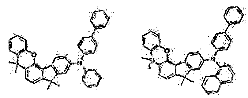 [A-169]
- [규칙 제91조에 의한 정정 24.09.2013]
[규칙 제91조에 의한 정정 11.07.2013]
제1항에 있어서,상기 유기광전자소자용 화합물은 하기 화학식 B-10, B-11 또는 B-19 중 어느 하나로 표시되는 것인 유기광전자소자용 화합물.[B-10] [B-11]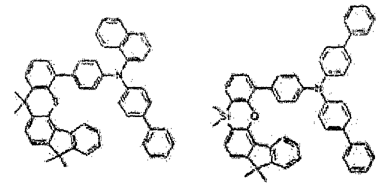 [B-19]
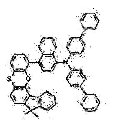
- [규칙 제91조에 의한 정정 24.09.2013]
제1항에 있어서,상기 유기광전자소자용 화합물은 하기 화학식 D-5 또는 D-20 중 어느 하나로 표시되는 것인 유기광전자소자용 화합물.[D-5] [D-20]

- 제1항 내지 제10항 중 어느 한 항에 있어서,상기 유기광전자소자용 화합물은 3중항 여기에너지(T1) 2.0eV 이상인 것인 유기광전자소자용 화합물.
- 제1항 내지 제10항 중 어느 한 항에 있어서,상기 유기광전자소자는, 유기광전소자, 유기발광소자, 유기태양전지, 유기트랜지스터, 유기 감광체 드럼 및 유기메모리소자로 이루어진 군에서 선택되는 것인 유기광전자소자용 화합물.
- 양극, 음극 및 상기 양극과 음극 사이에 개재되는 적어도 한 층 이상의 유기박막층을 포함하는 유기발광소자에 있어서,상기 유기박막층 중 적어도 어느 한 층은 상기 제1항 내지 제10항 중 어느 한 항에 따른 유기광전자소자용 화합물을 포함하는 것인 유기발광소자.
- 제13항에 있어서,상기 유기박막층은 발광층, 정공수송층, 정공주입층, 전자수송층, 전자주입층, 정공차단층 및 이들의 조합으로 이루어진 군에서 선택되는 것인 유기발광소자.
- 제13항에 있어서,상기 유기광전자소자용 화합물은 정공수송층 또는 정공주입층 내에 포함되는 것인 유기발광소자.
- 제13항에 있어서,상기 유기광전자소자용 화합물은 발광층 내에 포함되는 것인 유기발광소자.
- 제13항에 있어서,상기 유기광전자소자용 화합물은 발광층 내에 인광 또는 형광 호스트 재료로서 사용되는 것인 유기발광소자.
- 제13항의 유기발광소자를 포함하는 표시장치.
Priority Applications (4)
| Application Number | Priority Date | Filing Date | Title |
|---|---|---|---|
| EP13840477.7A EP2902463B1 (en) | 2012-09-28 | 2013-05-06 | Compound for organic optoelectronic device, organic light-emitting device, and display device |
| CN201380048168.3A CN105121594B (zh) | 2012-09-28 | 2013-05-06 | 用于有机光电装置的化合物、包含其的有机发光装置以及包括所述有机发光装置的显示装置 |
| JP2015534376A JP6167180B2 (ja) | 2012-09-28 | 2013-05-06 | 有機光電子素子用化合物、これを含む有機発光素子および前記有機発光素子を含む表示装置 |
| US14/610,005 US9368733B2 (en) | 2012-09-28 | 2015-01-30 | Compound for organic optoelectronic device, organic light-emitting device containing the same, and display device including said organic light-emitting device |
Applications Claiming Priority (2)
| Application Number | Priority Date | Filing Date | Title |
|---|---|---|---|
| KR10-2012-0109449 | 2012-09-28 | ||
| KR1020120109449A KR101537005B1 (ko) | 2012-09-28 | 2012-09-28 | 유기광전자소자용 화합물, 이를 포함하는 유기발광소자 및 상기 유기발광소자를 포함하는 표시장치 |
Related Child Applications (1)
| Application Number | Title | Priority Date | Filing Date |
|---|---|---|---|
| US14/610,005 Continuation US9368733B2 (en) | 2012-09-28 | 2015-01-30 | Compound for organic optoelectronic device, organic light-emitting device containing the same, and display device including said organic light-emitting device |
Publications (2)
| Publication Number | Publication Date |
|---|---|
| WO2014051232A1 true WO2014051232A1 (ko) | 2014-04-03 |
| WO2014051232A9 WO2014051232A9 (ko) | 2015-04-30 |
Family
ID=50388580
Family Applications (1)
| Application Number | Title | Priority Date | Filing Date |
|---|---|---|---|
| PCT/KR2013/003897 WO2014051232A1 (ko) | 2012-09-28 | 2013-05-06 | 유기광전자소자용 화합물, 이를 포함하는 유기발광소자 및 상기 유기발광소자를 포함하는 표시장치 |
Country Status (6)
| Country | Link |
|---|---|
| US (1) | US9368733B2 (ko) |
| EP (1) | EP2902463B1 (ko) |
| JP (1) | JP6167180B2 (ko) |
| KR (1) | KR101537005B1 (ko) |
| CN (1) | CN105121594B (ko) |
| WO (1) | WO2014051232A1 (ko) |
Cited By (9)
| Publication number | Priority date | Publication date | Assignee | Title |
|---|---|---|---|---|
| JP2016505518A (ja) * | 2012-11-12 | 2016-02-25 | メルク パテント ゲーエムベーハー | 電子素子のための材料 |
| WO2015178740A3 (ko) * | 2014-05-22 | 2016-06-16 | 주식회사 엘지화학 | 헤테로환 화합물 및 이를 포함하는 유기발광소자 |
| EP3053918A1 (en) * | 2015-02-06 | 2016-08-10 | Idemitsu Kosan Co., Ltd | 2-carbazole substituted benzimidazoles for electronic applications |
| US20170170406A1 (en) * | 2014-04-09 | 2017-06-15 | Doosan Corporation | Organic compound and organic electroluminescent element comprising same |
| JP2018503619A (ja) * | 2014-12-22 | 2018-02-08 | メルク パテント ゲーエムベーハー | 電子素子のための材料 |
| JP2019503364A (ja) * | 2015-12-24 | 2019-02-07 | ドゥーサン コーポレイション | 有機化合物およびこれを含む有機電界発光素子 |
| JP2019505513A (ja) * | 2016-01-27 | 2019-02-28 | エルジー・ケム・リミテッド | スピロ型化合物およびこれを含む有機電子素子 |
| US10566547B2 (en) | 2016-07-11 | 2020-02-18 | Universal Display Corporation | Organic electroluminescent materials and devices |
| KR20220008927A (ko) * | 2019-12-19 | 2022-01-21 | 산시 라이트 옵토일렉스로닉스 머터리얼 코포레이션 리미티드 | 유기 화합물,전자 소자 및 전자 장치 |
Families Citing this family (23)
| Publication number | Priority date | Publication date | Assignee | Title |
|---|---|---|---|---|
| KR20140108117A (ko) * | 2013-02-28 | 2014-09-05 | 에스에프씨 주식회사 | 유기발광 화합물 및 이를 포함하는 유기전계발광소자 |
| JP6023635B2 (ja) * | 2013-04-15 | 2016-11-09 | 出光興産株式会社 | 縮合環アミン化合物及びそれを用いた有機エレクトロルミネッセンス素子 |
| KR101863942B1 (ko) | 2015-08-28 | 2018-07-06 | 삼성디스플레이 주식회사 | 축합환 화합물 및 이를 포함한 유기 발광 소자 |
| KR20180007042A (ko) * | 2016-07-11 | 2018-01-22 | 삼성디스플레이 주식회사 | 축합환 화합물 및 이를 포함한 유기 발광 소자 |
| KR102599413B1 (ko) * | 2016-07-11 | 2023-11-08 | 솔루스첨단소재 주식회사 | 유기 화합물 및 이를 포함하는 유기 전계 발광 소자 |
| KR102057303B1 (ko) * | 2016-11-04 | 2019-12-18 | 주식회사 엘지화학 | 신규한 헤테로 고리 화합물 및 이를 이용한 유기발광 소자 |
| CN106800515B (zh) * | 2016-12-08 | 2018-06-05 | 烟台九目化学制品有限公司 | 一种具有芴胺结构的有机电致发光材料及其应用 |
| KR102389254B1 (ko) * | 2017-05-16 | 2022-04-22 | 삼성디스플레이 주식회사 | 헤테로환 화합물 및 이를 포함하는 유기 전계 발광 소자 |
| CN107188873A (zh) * | 2017-06-12 | 2017-09-22 | 长春海谱润斯科技有限公司 | 一种含螺环结构的磷光主体材料及有机发光器件 |
| WO2019054634A1 (ko) * | 2017-09-12 | 2019-03-21 | 주식회사 엘지화학 | 신규한 헤테로 고리 화합물 및 이를 이용한 유기발광 소자 |
| KR102075732B1 (ko) * | 2017-09-12 | 2020-02-10 | 주식회사 엘지화학 | 신규한 헤테로 고리 화합물 및 이를 이용한 유기발광 소자 |
| KR102436431B1 (ko) * | 2017-09-21 | 2022-08-29 | 삼성디스플레이 주식회사 | 방향족 화합물 및 이를 포함하는 유기 전계 발광 소자 |
| CN108675975A (zh) * | 2017-10-17 | 2018-10-19 | 默克专利有限公司 | 用于有机电致发光器件的材料 |
| KR102103506B1 (ko) * | 2017-10-18 | 2020-04-22 | 주식회사 엘지화학 | 신규한 헤테로 고리 화합물 및 이를 이용한 유기발광 소자 |
| WO2019078461A1 (ko) * | 2017-10-18 | 2019-04-25 | 주식회사 엘지화학 | 신규한 헤테로 고리 화합물 및 이를 이용한 유기발광 소자 |
| WO2019078462A1 (ko) * | 2017-10-18 | 2019-04-25 | 주식회사 엘지화학 | 신규한 헤테로 고리 화합물 및 이를 이용한 유기발광 소자 |
| KR102103505B1 (ko) * | 2017-10-18 | 2020-04-22 | 주식회사 엘지화학 | 신규한 헤테로 고리 화합물 및 이를 이용한 유기발광 소자 |
| CN107721977A (zh) * | 2017-10-30 | 2018-02-23 | 华南协同创新研究院 | 含噻蒽五元稠环单元衍生物及其合成方法与应用 |
| KR102092266B1 (ko) * | 2018-07-20 | 2020-03-23 | 주식회사 엘지화학 | 신규한 화합물 및 이를 이용한 유기발광 소자 |
| WO2020106028A1 (ko) * | 2018-11-19 | 2020-05-28 | 주식회사 엘지화학 | 다환 화합물 및 이를 포함하는 유기 발광 소자 |
| CN111004207A (zh) * | 2019-12-19 | 2020-04-14 | 陕西莱特光电材料股份有限公司 | 有机化合物、电子器件及电子装置 |
| KR20210086155A (ko) * | 2019-12-31 | 2021-07-08 | 엘지디스플레이 주식회사 | 발광 물질 및 그를 이용한 전계 발광 표시 장치 |
| CN116217608B (zh) * | 2023-05-08 | 2023-08-18 | 浙江华显光电科技有限公司 | 含硅化合物及其在有机发光装置的应用 |
Citations (6)
| Publication number | Priority date | Publication date | Assignee | Title |
|---|---|---|---|---|
| JP2009267257A (ja) * | 2008-04-28 | 2009-11-12 | Idemitsu Kosan Co Ltd | 有機エレクトロルミネッセンス素子用材料及びそれを用いた有機エレクトロルミネッセンス素子 |
| WO2010050779A1 (en) * | 2008-10-30 | 2010-05-06 | Gracel Display Inc. | Novel organic electroluminescent compounds and organic electroluminescent device using the same |
| WO2011016648A1 (en) * | 2009-08-04 | 2011-02-10 | Rohm And Haas Electronic Materials Korea Ltd. | Novel organic electroluminescent compounds and organic electroluminescent device using the same |
| KR20110079402A (ko) * | 2009-12-31 | 2011-07-07 | (주)씨에스엘쏠라 | 유기 광소자 및 이를 위한 유기 광합물 |
| JP2011178742A (ja) * | 2010-03-03 | 2011-09-15 | Hodogaya Chem Co Ltd | フェノキサジン環構造またはフェノチアジン環構造を有する化合物および有機エレクトロルミネッセンス素子 |
| KR20120078301A (ko) * | 2010-12-31 | 2012-07-10 | 제일모직주식회사 | 유기광전소자용 화합물 및 이를 포함하는 유기광전소자 |
Family Cites Families (14)
| Publication number | Priority date | Publication date | Assignee | Title |
|---|---|---|---|---|
| US20040131881A1 (en) * | 2002-12-31 | 2004-07-08 | Eastman Kodak Company | Complex fluorene-containing compounds for use in OLED devices |
| US7271406B2 (en) * | 2003-04-15 | 2007-09-18 | 3M Innovative Properties Company | Electron transport agents for organic electronic devices |
| US20060094859A1 (en) * | 2004-11-03 | 2006-05-04 | Marrocco Matthew L Iii | Class of bridged biphenylene polymers |
| WO2007015412A1 (ja) * | 2005-08-03 | 2007-02-08 | Nippon Steel Chemical Co., Ltd. | 複素環化合物及びこれを用いた有機電界発光素子 |
| KR20110058247A (ko) | 2009-11-26 | 2011-06-01 | 덕산하이메탈(주) | 오원자 헤테로 고리를 포함하는 화합물 및 이를 이용한 유기전기소자, 그 단말 |
| EP2180013A1 (en) | 2007-07-31 | 2010-04-28 | Sumitomo Chemical Company, Limited | Compound, method for producing the same, ink composition using the compound, thin film, organic transistor, and organic electroluminescent device |
| DE102008017591A1 (de) | 2008-04-07 | 2009-10-08 | Merck Patent Gmbh | Neue Materialien für organische Elektrolumineszenzvorrichtungen |
| DE102008018670A1 (de) * | 2008-04-14 | 2009-10-15 | Merck Patent Gmbh | Neue Materialien für organische Elektrolumineszenzvorrichtungen |
| JP5544103B2 (ja) | 2009-03-04 | 2014-07-09 | 出光興産株式会社 | 芳香族化合物、有機電子素子用材料及びそれを用いた有機エレクトロルミネッセンス素子 |
| DE102009023155A1 (de) | 2009-05-29 | 2010-12-02 | Merck Patent Gmbh | Materialien für organische Elektrolumineszenzvorrichtungen |
| KR101115036B1 (ko) | 2009-08-18 | 2012-03-06 | 덕산하이메탈(주) | 티안트렌 구조를 가지는 화합물 및 이를 이용한 유기전기소자, 그 단말 |
| KR101324782B1 (ko) * | 2010-01-14 | 2013-10-31 | (주)씨에스엘쏠라 | 유기 광소자 및 이를 위한 유기 광합물 |
| DE102010048074A1 (de) * | 2010-10-09 | 2012-04-12 | Merck Patent Gmbh | Materialien für elektronische Vorrichtungen |
| KR20120070468A (ko) * | 2010-12-21 | 2012-06-29 | (주)씨에스엘쏠라 | 디하이드로안트라센계 유도체 및 이를 이용한 유기 광소자 |
-
2012
- 2012-09-28 KR KR1020120109449A patent/KR101537005B1/ko active IP Right Grant
-
2013
- 2013-05-06 WO PCT/KR2013/003897 patent/WO2014051232A1/ko active Application Filing
- 2013-05-06 JP JP2015534376A patent/JP6167180B2/ja active Active
- 2013-05-06 CN CN201380048168.3A patent/CN105121594B/zh active Active
- 2013-05-06 EP EP13840477.7A patent/EP2902463B1/en active Active
-
2015
- 2015-01-30 US US14/610,005 patent/US9368733B2/en active Active
Patent Citations (6)
| Publication number | Priority date | Publication date | Assignee | Title |
|---|---|---|---|---|
| JP2009267257A (ja) * | 2008-04-28 | 2009-11-12 | Idemitsu Kosan Co Ltd | 有機エレクトロルミネッセンス素子用材料及びそれを用いた有機エレクトロルミネッセンス素子 |
| WO2010050779A1 (en) * | 2008-10-30 | 2010-05-06 | Gracel Display Inc. | Novel organic electroluminescent compounds and organic electroluminescent device using the same |
| WO2011016648A1 (en) * | 2009-08-04 | 2011-02-10 | Rohm And Haas Electronic Materials Korea Ltd. | Novel organic electroluminescent compounds and organic electroluminescent device using the same |
| KR20110079402A (ko) * | 2009-12-31 | 2011-07-07 | (주)씨에스엘쏠라 | 유기 광소자 및 이를 위한 유기 광합물 |
| JP2011178742A (ja) * | 2010-03-03 | 2011-09-15 | Hodogaya Chem Co Ltd | フェノキサジン環構造またはフェノチアジン環構造を有する化合物および有機エレクトロルミネッセンス素子 |
| KR20120078301A (ko) * | 2010-12-31 | 2012-07-10 | 제일모직주식회사 | 유기광전소자용 화합물 및 이를 포함하는 유기광전소자 |
Non-Patent Citations (1)
| Title |
|---|
| See also references of EP2902463A4 * |
Cited By (19)
| Publication number | Priority date | Publication date | Assignee | Title |
|---|---|---|---|---|
| JP2016505518A (ja) * | 2012-11-12 | 2016-02-25 | メルク パテント ゲーエムベーハー | 電子素子のための材料 |
| US10957860B2 (en) | 2012-11-12 | 2021-03-23 | Merck Patent Gmbh | Materials for electronic devices |
| JP2018138544A (ja) * | 2012-11-12 | 2018-09-06 | メルク パテント ゲーエムベーハー | 電子素子のための材料 |
| US9978949B2 (en) | 2012-11-12 | 2018-05-22 | Merck Patent Gmbh | Materials for electronic devices |
| US20170170406A1 (en) * | 2014-04-09 | 2017-06-15 | Doosan Corporation | Organic compound and organic electroluminescent element comprising same |
| US10756277B2 (en) * | 2014-04-09 | 2020-08-25 | Doosan Solus Co., Ltd. | Organic compound and organic electroluminescent device comprising the same |
| CN106414454A (zh) * | 2014-05-22 | 2017-02-15 | 株式会社Lg化学 | 杂环化合物及包含其的有机发光器件 |
| US10003030B2 (en) | 2014-05-22 | 2018-06-19 | Lg Chem, Ltd. | Heterocyclic compound and organic light emitting device comprising same |
| WO2015178740A3 (ko) * | 2014-05-22 | 2016-06-16 | 주식회사 엘지화학 | 헤테로환 화합물 및 이를 포함하는 유기발광소자 |
| JP2018503619A (ja) * | 2014-12-22 | 2018-02-08 | メルク パテント ゲーエムベーハー | 電子素子のための材料 |
| EP3053918A1 (en) * | 2015-02-06 | 2016-08-10 | Idemitsu Kosan Co., Ltd | 2-carbazole substituted benzimidazoles for electronic applications |
| JP2019503364A (ja) * | 2015-12-24 | 2019-02-07 | ドゥーサン コーポレイション | 有機化合物およびこれを含む有機電界発光素子 |
| JP2019505513A (ja) * | 2016-01-27 | 2019-02-28 | エルジー・ケム・リミテッド | スピロ型化合物およびこれを含む有機電子素子 |
| US10968230B2 (en) | 2016-01-27 | 2021-04-06 | Lg Chem, Ltd. | Spiro-structured compound and organic electronic device comprising same |
| US10566547B2 (en) | 2016-07-11 | 2020-02-18 | Universal Display Corporation | Organic electroluminescent materials and devices |
| US10680184B2 (en) | 2016-07-11 | 2020-06-09 | Universal Display Corporation | Organic electroluminescent materials and devices |
| KR20220008927A (ko) * | 2019-12-19 | 2022-01-21 | 산시 라이트 옵토일렉스로닉스 머터리얼 코포레이션 리미티드 | 유기 화합물,전자 소자 및 전자 장치 |
| KR102397562B1 (ko) * | 2019-12-19 | 2022-05-13 | 산시 라이트 옵토일렉스로닉스 머터리얼 코포레이션 리미티드 | 유기 화합물,전자 소자 및 전자 장치 |
| US11605784B2 (en) | 2019-12-19 | 2023-03-14 | Shaanxi Lighte Optoelectronics Material Co., Ltd. | Organic compound, electronic element, and electronic device |
Also Published As
| Publication number | Publication date |
|---|---|
| JP6167180B2 (ja) | 2017-07-19 |
| WO2014051232A9 (ko) | 2015-04-30 |
| EP2902463A1 (en) | 2015-08-05 |
| EP2902463A4 (en) | 2016-07-13 |
| JP2016502500A (ja) | 2016-01-28 |
| EP2902463B1 (en) | 2019-10-23 |
| CN105121594A (zh) | 2015-12-02 |
| KR20140042554A (ko) | 2014-04-07 |
| CN105121594B (zh) | 2017-03-22 |
| US20150137111A1 (en) | 2015-05-21 |
| KR101537005B1 (ko) | 2015-07-20 |
| US9368733B2 (en) | 2016-06-14 |
Similar Documents
| Publication | Publication Date | Title |
|---|---|---|
| WO2014051232A1 (ko) | 유기광전자소자용 화합물, 이를 포함하는 유기발광소자 및 상기 유기발광소자를 포함하는 표시장치 | |
| WO2021107736A1 (ko) | 유기 발광 소자 | |
| WO2013094951A1 (ko) | 유기광전자소자용 화합물, 이를 포함하는 유기발광소자 및 상기 유기발광소자를 포함하는 표시장치 | |
| WO2018216990A1 (ko) | 유기화합물 및 이를 포함하는 유기전계발광소자 | |
| WO2014030822A1 (ko) | 유기광전자소자용 화합물, 이를 포함하는 유기발광소자 및 상기 유기발광소자를 포함하는 표시장치 | |
| WO2013100467A1 (ko) | 유기광전자소자용 화합물, 이를 포함하는 유기발광소자 및 상기 유기발광소자를 포함하는 표시장치 | |
| WO2013100538A1 (ko) | 유기광전자소자용 화합물, 이를 포함하는 유기발광소자 및 상기 유기발광소자를 포함하는 표시장치 | |
| WO2018097648A1 (ko) | 헤테로고리 화합물 및 이를 이용한 유기 발광 소자 | |
| WO2013183851A1 (ko) | 새로운 유기전계발광소자용 화합물 및 그를 포함하는 유기전계발광소자 | |
| EP3371182A1 (en) | Electron buffering materials, electron transport materials and organic electroluminescent device comprising the same | |
| WO2013089424A1 (ko) | 유기광전자소자용 화합물, 이를 포함하는 유기발광소자 및 상기 유기발광소자를 포함하는 표시장치 | |
| EP2697216A1 (en) | Novel compounds for organic electronic material and organic electroluminescent device using the same | |
| WO2021107699A9 (ko) | 유기 발광 소자 | |
| WO2010005266A2 (ko) | 신규한 안트라센 유도체 및 이를 이용한 유기 전자 소자 | |
| WO2014058123A1 (ko) | 유기광전자소자용 화합물, 이를 포함하는 유기발광소자 및 상기 유기발광소자를 포함하는 표시장치 | |
| WO2012141393A9 (ko) | 유기광전자소자용 화합물, 이를 포함하는 유기발광소자 및 상기 유기발광소자를 포함하는 표시장치 | |
| WO2013095039A1 (ko) | 유기광전자소자용 화합물, 이를 포함하는 유기발광소자 및 상기 유기발광소자를 포함하는 표시장치 | |
| WO2013100540A1 (ko) | 유기광전자소자용 화합물, 이를 포함하는 유기발광소자 및 상기 유기발광소자를 포함하는 표시장치 | |
| WO2012015265A1 (en) | Novel organic electroluminescent compounds and organic electroluminescent device using the same | |
| WO2021107359A1 (ko) | 화합물 및 이를 포함하는 유기 발광 소자 | |
| WO2013032297A1 (en) | Benzocarbazole compounds and electroluminescent devices involving them | |
| WO2013100465A1 (ko) | 유기광전자소자용 화합물, 이를 포함하는 유기발광소자 및 상기 유기발광소자를 포함하는 표시장치 | |
| WO2013187689A1 (en) | Novel organic electroluminescent compounds and organic electroluminescent device comprising the same | |
| WO2013022145A9 (ko) | 유기광전자소자용 화합물 및 이를 포함하는 유기발광소자 | |
| WO2020022771A1 (ko) | 유기 발광 소자 |
Legal Events
| Date | Code | Title | Description |
|---|---|---|---|
| 121 | Ep: the epo has been informed by wipo that ep was designated in this application |
Ref document number: 13840477 Country of ref document: EP Kind code of ref document: A1 |
|
| ENP | Entry into the national phase |
Ref document number: 2015534376 Country of ref document: JP Kind code of ref document: A |
|
| NENP | Non-entry into the national phase |
Ref country code: DE |
|
| WWE | Wipo information: entry into national phase |
Ref document number: 2013840477 Country of ref document: EP |