WO2014050326A1 - 電子顕微鏡および電子線検出器 - Google Patents
電子顕微鏡および電子線検出器 Download PDFInfo
- Publication number
- WO2014050326A1 WO2014050326A1 PCT/JP2013/071611 JP2013071611W WO2014050326A1 WO 2014050326 A1 WO2014050326 A1 WO 2014050326A1 JP 2013071611 W JP2013071611 W JP 2013071611W WO 2014050326 A1 WO2014050326 A1 WO 2014050326A1
- Authority
- WO
- WIPO (PCT)
- Prior art keywords
- scintillator
- light guide
- electron microscope
- electron
- end surface
- Prior art date
- Legal status (The legal status is an assumption and is not a legal conclusion. Google has not performed a legal analysis and makes no representation as to the accuracy of the status listed.)
- Ceased
Links
Images





Classifications
-
- H—ELECTRICITY
- H01—ELECTRIC ELEMENTS
- H01J—ELECTRIC DISCHARGE TUBES OR DISCHARGE LAMPS
- H01J37/00—Discharge tubes with provision for introducing objects or material to be exposed to the discharge, e.g. for the purpose of examination or processing thereof
- H01J37/26—Electron or ion microscopes; Electron or ion diffraction tubes
- H01J37/28—Electron or ion microscopes; Electron or ion diffraction tubes with scanning beams
-
- H—ELECTRICITY
- H01—ELECTRIC ELEMENTS
- H01J—ELECTRIC DISCHARGE TUBES OR DISCHARGE LAMPS
- H01J37/00—Discharge tubes with provision for introducing objects or material to be exposed to the discharge, e.g. for the purpose of examination or processing thereof
- H01J37/02—Details
- H01J37/22—Optical, image processing or photographic arrangements associated with the tube
-
- H—ELECTRICITY
- H01—ELECTRIC ELEMENTS
- H01J—ELECTRIC DISCHARGE TUBES OR DISCHARGE LAMPS
- H01J2237/00—Discharge tubes exposing object to beam, e.g. for analysis treatment, etching, imaging
- H01J2237/06—Sources
- H01J2237/063—Electron sources
-
- H—ELECTRICITY
- H01—ELECTRIC ELEMENTS
- H01J—ELECTRIC DISCHARGE TUBES OR DISCHARGE LAMPS
- H01J2237/00—Discharge tubes exposing object to beam, e.g. for analysis treatment, etching, imaging
- H01J2237/244—Detection characterized by the detecting means
- H01J2237/2443—Scintillation detectors
-
- H—ELECTRICITY
- H01—ELECTRIC ELEMENTS
- H01J—ELECTRIC DISCHARGE TUBES OR DISCHARGE LAMPS
- H01J2237/00—Discharge tubes exposing object to beam, e.g. for analysis treatment, etching, imaging
- H01J2237/244—Detection characterized by the detecting means
- H01J2237/2445—Photon detectors for X-rays, light, e.g. photomultipliers
-
- H—ELECTRICITY
- H01—ELECTRIC ELEMENTS
- H01J—ELECTRIC DISCHARGE TUBES OR DISCHARGE LAMPS
- H01J2237/00—Discharge tubes exposing object to beam, e.g. for analysis treatment, etching, imaging
- H01J2237/26—Electron or ion microscopes
- H01J2237/28—Scanning microscopes
-
- H—ELECTRICITY
- H01—ELECTRIC ELEMENTS
- H01J—ELECTRIC DISCHARGE TUBES OR DISCHARGE LAMPS
- H01J2237/00—Discharge tubes exposing object to beam, e.g. for analysis treatment, etching, imaging
- H01J2237/26—Electron or ion microscopes
- H01J2237/28—Scanning microscopes
- H01J2237/2801—Details
-
- H—ELECTRICITY
- H01—ELECTRIC ELEMENTS
- H01J—ELECTRIC DISCHARGE TUBES OR DISCHARGE LAMPS
- H01J37/00—Discharge tubes with provision for introducing objects or material to be exposed to the discharge, e.g. for the purpose of examination or processing thereof
- H01J37/02—Details
- H01J37/244—Detectors; Associated components or circuits therefor
Definitions
- the present invention relates to an electron microscope and an electron beam detector used for the electron microscope.
- the observation target region on the sample surface is scanned two-dimensionally with the primary electron beam, and signal electrons emitted from the irradiation position of the primary electron beam are detected.
- a scanning electron microscope that generates and displays a two-dimensional image of a scanned observation target region by mapping and displaying the detection signal in synchronization with the scanning position of the primary electron beam is widely known.
- the signal electrons emitted from the sample surface are roughly classified into secondary electrons and reflected electrons according to the energy.
- Reflected electrons refer to electrons emitted from the sample surface again after incident electrons repeat elastic scattering and inelastic scattering in the sample. Therefore, the reflected electrons have a generated peak with the same energy as the incident electrons.
- secondary electrons indicate those emitted from the sample surface among the low-energy electrons generated when reflected electrons cause inelastic scattering. Therefore, the secondary electrons have a generated peak with energy of about several eV.
- signal electrons having an energy of less than 50 eV are called secondary electrons and are distinguished from reflected electrons.
- the observation image (secondary electron image) of the sample based on secondary electrons and the observation image (reflected electron image) of the sample based on reflected electrons contain different information. ing. That is, the secondary electron image is an observation image in which information on the unevenness of the sample surface and the potential is emphasized, whereas the reflected electron image is an observation image in which information on the composition and crystal orientation of the sample is emphasized.
- the amount of energy generated is small, so that the amount generated is easily affected by the shape and surface potential of the sample surface, whereas in the case of reflected electrons, the amount generated is the average of the sample. This depends on the atomic number.
- channeling contrast observed when a sample having the same composition has a partially different crystal orientation on the sample surface or includes a crystal defect or the like is derived from reflected electrons.
- Scanning electron microscopes have been required to capture not only the unevenness of the sample surface, but also the contrast and channeling contrast representing the composition of the sample more clearly. That is, in a scanning electron microscope, there has been a demand for a method for easily obtaining an observation image of a sample based on reflected electrons with high sensitivity, high speed, and simplicity.
- the electron beam detector needs to be disposed immediately above the sample.
- a scintillator made of a single crystal as disclosed in Patent Document 1 has been used as such an electron beam detector because of the necessity of reducing the electron beam detector.
- Patent Documents 2-4 disclose a method of separating reflected electrons and secondary electrons based on energy and orbital differences.
- the scintillator made of a single crystal has problems such as difficulty in processing, lack of freedom of shape forming, and high cost. Further, if the reflected electrons and the secondary electrons are only separated based on the difference in energy and orbit, the yield of detected reflected electrons is reduced, and there is a problem in detection sensitivity and response speed.
- an object of the present invention is to provide an electron beam detector capable of improving the sensitivity and response speed of backscattered electron detection, and an electron microscope to which the electron beam detector is applied. Is to provide.
- An electron microscope is a plate-like scintillator that emits fluorescence when incident on an electron beam, a light guide that has a refractive index smaller than the refractive index of the scintillator, and guides the fluorescence emitted by the scintillator,
- the scintillator is characterized in that a part of an end surface is formed as an outwardly convex curved surface and is joined to the light guide via the convex curved end surface.
- the scintillator has a composition formula (Ln 1-x Ce x ) 3 M 5 O 12 (where Ln represents at least one element selected from Y, Gd, La and Lu, and M represents Al and It represents a Y—Al—O-based ceramic sintered body represented by (representing at least one element selected from Ga).
- FIGS. 3A and 3B are diagrams illustrating examples of shapes of a scintillator and a light guide used in the electron microscope according to the present embodiment, FIG. 3A is an example of a top view, and FIG. 3B is an example of a side view.
- FIG. 4A is a diagram illustrating an example of the shape of a scintillator according to a first modification of the embodiment of the present invention, FIG. 4A is an example of a top view, and FIG.
- FIG. 4B is an example of a side view. It is the figure which showed the example of the shape of the scintillator which concerns on the 2nd modification of embodiment of this invention, FIG. 5 (A) is an example of a top view, FIG.5 (B) is an example of a side view.
- FIG. 6A is a view showing an example of the shape of a scintillator according to a third modification of the embodiment of the present invention, FIG. 6A is an example of a top view, and FIG. 6B is an example of a side view. It is the figure which showed the example of the shape of the scintillator which concerns on the 4th modification of embodiment of this invention, FIG.
- FIG. 7 (A) is an example of a top view
- FIG.7 (B) is an example of a side view.
- FIG. 8 (A) is an example of a top view
- FIG.8 (B) is an example of a side view.
- FIG. 1 is a diagram illustrating an example of a main configuration of an electron microscope 100 according to an embodiment of the present invention.
- the main part of the electron microscope 100 according to the embodiment of the present invention includes a scanning lens 2, an objective lens 3, a sample chamber 4, a scintillator 7, a light guide 8, a photoelectric conversion element 9, an amplification circuit 10,
- the display device 14 is included.
- a sample table (not shown) for holding the sample 5 and a sample table moving mechanism (not shown) for moving the sample table to determine the observation target area of the sample 5 are provided.
- the sample 5 is disposed immediately below the objective lens 3 in the sample chamber 4.
- the scintillator 7 is disposed between the objective lens 3 and the sample 5.
- the primary electron beam 1 emitted from an electron gun (not shown) is deflected by the scanning lens 2 in order to scan the observation target region of the sample 5 and is focused by the objective lens 3. Together, the surface of the sample 5 is irradiated.
- an electron passage hole 71 is provided at a position in the vicinity of which the primary electron beam 1 passes through the center of the scintillator 7, and the primary electron beam 1 passes through the electron passage hole 71 and passes through the sample 5. Irradiate the surface.
- the lower surface of the scintillator 7 is hereinafter referred to as an electron incident surface 75.
- the objective lens 3 is, for example, a semi-in lens type.
- secondary electrons (not shown) are wound up along the optical axis of the primary electron beam 1 by the strong magnetic field of the objective lens 3, pass through the electron passage hole 71 from the bottom to the top, and further, the objective lens 3.
- the amount of incident light on the scintillator 7 is small.
- the scintillator 7 When the reflected electrons 6 are incident on the scintillator 7, the scintillator 7 that is a phosphor emits fluorescence.
- the fluorescence emitted from the scintillator 7 is guided by the light guide 8, enters the photoelectric conversion element 9 including a photomultiplier tube and a semiconductor light receiving element, and is converted into an electric signal by the photoelectric conversion element 9.
- a signal (backscattered electron detection signal) corresponding to the amount of backscattered electrons thus converted into an electrical signal is amplified by the amplifier circuit 10 and transmitted to the display device 14.
- an electron beam detector 12 a portion including the scintillator 7, the light guide 8, the photoelectric conversion element 9, and the amplifier circuit 10 is referred to as an electron beam detector 12 (however, the amplifier circuit 10 is included in the electron beam detector 12). May not be)
- a Y—Al—O ceramic sintered body using Ce as an activator is used as the material of the scintillator 7.
- the Y—Al—O ceramic sintered body using Ce as an activator is a ceramic sintered body obtained by sintering a material represented by the composition formula (Ln 1-x Ce x ) 3 M 5 O 12 Refers to the body.
- Ln represents at least one element of Y, Gd, La, and Lu
- M represents at least one element of Al and Ga.
- the Ce composition ratio x is in the range of 0.002 ⁇ x ⁇ 0.025. The basis for this will be described separately with reference to the drawings.
- the Y—Al—O-based ceramic sintered body as described above is a mixture of oxide powders as raw materials, pressed into an appropriate shape, and constant at an appropriate temperature, for example, 1400 ° C. to 1600 ° C. It can be manufactured by a method such as holding for a period of time. In addition, as the raw material, it is possible to use ultrafine particles obtained by solution precipitation.
- the single crystal material generally used conventionally as a material of the scintillator 7 is manufactured by a method such as pulling up from the melt, it takes time and effort to manufacture, and the size and shape are also increased. Will be limited. That is, a single crystal material manufactured by crystal growth by pulling has a cylindrical shape, and if the diameter is increased, there is a further problem that the apparatus cost increases. Therefore, in the case of a single crystal material, the shape of the scintillator 7 generally has to be a disc shape with a round periphery. However, in the case of the disc-shaped scintillator 7, since emitted fluorescence is emitted in all directions, there is a problem that the amount of incident light on the light guide 8 cannot be increased because of a large loss of light amount.
- the square scintillator 7 With a single crystal material. However, in that case, a rectangular plate is cut out from a disc that is not so large, and the peripheral portion is discarded, so that the material loss increases and the cost of the material increases.
- the scintillator 7 using the Y—Al—O ceramic sintered body can be manufactured at a relatively low cost because it is only necessary to press the material powder into an appropriate shape and sinter it. Moreover, since the shape as a ceramic is substantially determined by the shape when the powder is pressed, a large degree of freedom can be obtained in designing the size and shape of the scintillator 7. Therefore, by devising the shape of the scintillator 7, it is possible to reduce the loss of light quantity in the scintillator 7, increase the incident light quantity to the light guide 8, and the like.
- the Y—Al—O ceramic sintered body is polycrystalline and is basically an aggregate of microcrystals having various crystal orientations, the sintered body as a whole has characteristics of crystal anisotropy. None appear. Therefore, unlike the single crystal material having the same crystal orientation as a whole, the manufacturing cost can be reduced because the crystal orientation need not be taken into consideration.
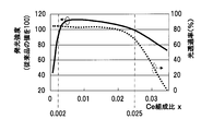
- FIG. 2 is a graph showing an example of a Ce composition ratio dependence characteristic graph of fluorescence emission intensity and light transmittance of a Y—Al—O-based ceramic sintered body.
- the horizontal axis of the graph is Ce composition ratio x
- the left vertical axis represents fluorescence emission intensity
- the right vertical axis represents light transmittance
- the thick solid line curve represents measured values of fluorescence emission intensity
- a thick dotted curve represents light transmittance.
- the measured value of the luminescence intensity was obtained when a thin plate (20 mm square, 2 mm thickness) of a Y—Al—O ceramic sintered body was irradiated with an electron beam accelerated at 10 kV.
- the measured value is expressed as a relative value when the emission intensity of a conventionally used single crystal scintillator is 100.
- the dependence characteristic with respect to Ce composition ratio x of such emitted light intensity shows not only the electron beam accelerated by 10 kV but the same tendency also about the electron beam which has various energy.
- the measured value of the light transmittance is a light with a wavelength in the range of 500 to 650 nm, particularly light with a wavelength of around 550 nm incident on a thin plate (20 mm square, thickness 2 mm) of a Y—Al—O ceramic sintered body. This is what you get.
- the Y—Al—O ceramic sintered body used in the present embodiment emits fluorescence having a wavelength in the range of 500 to 650 nm when irradiated with an electron beam.
- the Y—Al—O-based ceramic sintered body exhibits emission intensity exceeding that of the conventional single crystal scintillator when the Ce composition ratio x is in the range of 0.002 to 0.025. I understand that.
- the light transmittance generally shows a value of 80% or more when the Ce composition ratio x is 0.02 or less, and when the Ce composition ratio x exceeds 0.02, the value falls below 80%.
- the Ce composition ratio x is in the range of 0.025 or less, a value greater than 60% is exhibited. Therefore, it can be said that the light transmittance of the Y—Al—O ceramic sintered body is good when the Ce composition ratio x is 0.025 or less.
- the emission intensity and light transmittance data in the graph of FIG. 2 are obtained when the Y—Al—O based ceramic sintered body is a substance represented by the composition formula (Y 1-x Ce x ) 3 Al 5 O 12.
- the composition formula is represented by (Ln 1-x Ce x ) 3 M 5 O 12
- Ln is at least one element of Y, Gd, La and Lu
- M is In the case of at least one element of Al and Ga, substantially the same data is obtained.
- a Y—Al—O based ceramic sintered body represented by the composition formula (Ln 1-x Ce x ) 3 M 5 O 12 (where Ln is Y, Gd, A scintillator in which at least one element of La and Lu and M is at least one element of Al and Ga and the composition ratio x of Ce is in the range of 0.002 ⁇ x ⁇ 0.025 7 is used as a material.
- the material of the light guide 8 a material having high transparency such as acrylic resin, polycarbonate resin, plate glass, and quartz glass is used. Moreover, you may use the light guide which can be made into a curve like an optical fiber.
- the scintillator 7 and the light guide 8 may be a gap or may be joined with a joining material such as a transparent resin, optical cement, or matching oil interposed.
- the electron beam detector 12 including the scintillator 7 and the light guide 8 is Performance such as high sensitivity and fast response speed can be obtained.
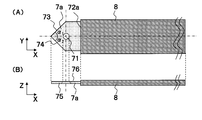
- FIGS. 3A and 3B are diagrams showing examples of the shapes of the scintillator 7 and the light guide 8 used in the electron microscope 100 according to the present embodiment.
- FIG. 3A is an example of a top view
- FIG. 3B is a side view. It is an example.
- FIGS. 3A and 3B only the shape of the light guide 8 in the vicinity of being connected to the scintillator 7 is shown.
- the length direction of the light guide 8 is taken as the X axis, and the width direction of the light guide 8 is taken as the Y axis.
- the length direction of the light guide 8 is taken as the X axis, and the thickness direction of the light guide 8 and the scintillator 7 is taken as the Z axis. This also applies to the drawings subsequent to FIG.
- the scintillator 7 has an electron passage hole 71 for allowing the primary electron beam 1 and the like to pass therethrough in the center thereof, and also has the following features. have.
- the first feature is that, of the end surfaces of the scintillator 7, the end surface 72 joined to the light guide 8 is formed as a convex curved surface on the outside.
- the scintillator 7 and the light guide 8 may be joined with a gap (that is, an air or vacuum layer), or a joining material such as transparent resin, optical cement, or matching oil is packed in the gap. You may join.
- the second feature is that the end surface of the scintillator 7 on the side opposite to the end joined to the light guide 8 is substantially parallel to the Z axis, and the angle ⁇ 1 and angle with the X axis, respectively. That is, the two end faces 73 and 74 forming ⁇ 2 are formed. Note that the angle ⁇ 1 and the angle ⁇ 2 may be the same value or different values. However, it is assumed that ⁇ 1 + ⁇ 2 ⁇ 180 degrees.
- the third feature is that the upper surface 76 of the scintillator 7 facing the electron incident surface 75 (the lower surface of the scintillator 7) of the scintillator 7 is inclined with respect to the electron incident surface 75 at an inclination angle ⁇ . It is. In this case, the thickness of the scintillator 7 is larger (thicker) closer to the end surface 72 facing the light guide 8, and decreases (thinner) away from the end surface 72.
- a metal film that acts as a light reflecting film is formed on the surface of the scintillator 7 having the above-described shape features on the surface other than the end face 72 joined to the light guide 8.
- the material of the metal film may be any metal as long as it reflects light and has a high reflectance, but Al is generally used.
- a metal film such as an Al film can be formed by vacuum deposition or the like.
- the scintillator 7 has a shape having the above-described characteristics, and a metal film such as an Al film is formed on the surface other than the end face 72 joined to the light guide 8, both of which occur in the scintillator 7. This is intended to make as much fluorescence as possible incident on the light guide 8.
- a metal film such as an Al film
- a metal film such as an Al film formed on the surface of the scintillator 7 acts as a light reflecting film, and prevents the fluorescence generated in the scintillator 7 from escaping to the outside. That is, a metal film such as an Al film has an effect of suppressing loss of the amount of fluorescent light generated in the scintillator 7. Further, the metal film formed on the surface of the scintillator 7 is made conductive to the housing of the electron microscope 100 or the like, thereby preventing the scintillator 7 from being charged up, and the detection signal S / S based on the reflected electrons 6 incident on the scintillator 7. Effects such as improving N (Signal ⁇ to Noise Ratio) can also be expected.
- the film thickness of the metal film formed on the electron incident surface 75 (the lower surface of the scintillator 7) needs to be a film thickness that does not prevent the incident of the reflected electrons 6. . That is, the film thickness of the metal film is required to reflect light sufficiently and allow the reflected electrons 6 to enter. Furthermore, the film thickness is required to be a thickness that shields secondary electrons having energy of 50 eV or less.
- the film thickness of the metal film that satisfies the above conditions is desirably about 100 nm or less and about 50 nm.
- an Al film having a target thickness of 50 nm is formed on the electron incident surface 75 of the scintillator 7.
- the film thickness should be thick. As a result, the reflectance of the light is improved, and the amount of the fluorescent light generated in the scintillator 7 can be reduced.
- the film thickness is preferably 100 nm or more.
- an Al film having a thickness of 200 nm is formed on the surface of the scintillator 7 except for the end face 72 and the electron incident surface 75 that are joined to the light guide 8.
- the upper surface 76 of the scintillator 7 is inclined with respect to the electron incident surface 75 at an inclination angle ⁇ (third feature), and the scintillator 7 is the light guide 8.
- the end face 73 and the end face 74 at the end opposite to the end joined to each other are inclined at an angle ⁇ 1 and an angle ⁇ 2 with respect to the X-axis, respectively (second feature). Accordingly, the fluorescence generated in the scintillator 7 is easily reflected in the direction toward the end face 72 joined to the light guide 8, and can reach the end face 72 by multiple reflections on the average.
- the angle ⁇ 1 and the angle ⁇ 2 formed by the end surface 73 and the end surface 74 at the end of the scintillator 7 are 30 degrees ⁇ ⁇ 1 , ⁇ 2 ⁇ 90 degrees. It was found that the fluorescence can be effectively guided to the end face 72. Similarly, it was found that when the inclination angle ⁇ formed by the upper surface 76 of the scintillator 7 with the electron incident surface 75 is 0 degree ⁇ ⁇ 60 degrees, the fluorescence can be effectively guided to the end face 72.
- the end surface 72 of the scintillator 7 is formed as a convex curved surface outward. This is related to the fact that the refractive index of the Y—Al—O ceramic sintered body using Ce, which is the material of the scintillator 7, as an activator is large.
- the refractive index of a Y—Al—O ceramic sintered body using Ce as an activator is about 1.8.
- the refractive index of a general transparent resin or glass used as the material of the light guide 8 is about 1.4 to 1.6, and the refractive index of a general optical cement or adhesive resin is about 1.6 or less.
- the refractive index of air or vacuum is approximately 1.
- the fluorescence emitted in the scintillator 7 enters the material having a small refractive index from the material having a large refractive index. In that case, if the fluorescent light emitted in the scintillator 7 makes an angle larger than a certain angle, the phenomenon of total reflection occurs and it cannot go out of the scintillator 7.
- the critical angle of total reflection is about 34 degrees.
- the fluorescence generated in the scintillator 7 is incident on the boundary surface (end surface 72) with the air or vacuum of the scintillator 7 at an incident angle larger than about 34 degrees, total reflection occurs, and the scintillator 7 I can't go outside.
- the critical angle of total reflection is about 63 degrees.
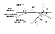
- the end face 72 of the scintillator 7 is formed with a convex curved surface outward, so that total reflection at the boundary surface is less likely to occur, and loss of light quantity at the boundary surface is reduced.
- the reason why it is difficult to cause total reflection at the boundary surface by forming the end surface 72 of the scintillator 7 as an outwardly convex curved surface will be described.
- FIG. 10 schematically shows the difference in the manner of total reflection between a flat boundary surface and a convex boundary surface on the outside when light goes out from a material with a large refractive index to a material with a small refractive index (including a vacuum).
- the material in the lower region (scintillator 7) has a high refractive index
- the material in the upper region has a low refractive index
- the lower region and the upper region have a flat (planar) boundary surface M1.
- the boundary is divided by a boundary surface M2 having a convex curved surface as viewed from the lower region side.
- the incident angle ⁇ 1 of the light ray from the point P to the point Q on the boundary surface M1 is the critical angle of total reflection. In that case, the light beam does not exit to the upper region where the refractive index is small.
- the incident angle ⁇ 1 is an angle formed by the light ray PQ and a straight line V1 passing through the point Q and perpendicular to the boundary surface M1.
- the boundary between the upper region and the lower region is an outwardly convex curved boundary surface M2
- the ray from the point P to the point Q on the surface corresponding to the boundary surface M1 is bounded at the point R. Intersects with M2.
- the incident angle ⁇ 2 of the ray PR with respect to the boundary surface M2 is an angle formed by the ray PR with respect to the straight line V2 passing through the point R perpendicular to the tangent plane H2 of the boundary surface M2 at the point R.
- a boundary surface M1 having a flat boundary with a light ray emitted from a point P this is a case where the boundary is a boundary surface M2 having a curved surface that is convex outward, even if the light ray is totally reflected. It means not totally reflecting. That is, when the shape of the end surface 72 joined to the light guide 8 of the scintillator 7 is a curved surface that is convex outward, the scintillator 7 has more fluorescence inside the scintillator 7 than when it is a flat surface. Will go out. That is, the amount of light emitted from the scintillator 7 increases.
- the curvature of the end face 72 is preferably 5% or more.
- the amount of fluorescence taken out from the scintillator 7 can be increased.
- the curvature rate c of the curved surface S refers to another point on the curved surface S that is separated from the point P (not shown) on the curved surface S by a distance d along the curved surface S (not shown).
- the end surface of the end other than the end surface 72 of the scintillator 7 (the end surface 73, the end surface 74, the end surface 78 that connects the end surface 72 and the end surface 73, and the end surface 79 that connects the end surface 72 and the end surface 74).
- a metal film for reflection is formed on these end faces, it is preferable that these end faces are inwardly concave curved surfaces in consideration of the ease of total reflection.
- the width (Y direction) of the end portion where the end surface 72 of the scintillator 7 is joined at the end portion of the light guide 8 is the end surface of the scintillator 7. It is assumed that it is larger than the width of the 72 portion.
- the thickness (Z direction) of the end portion where the end surface 72 of the scintillator 7 is joined at the end portion of the light guide 8 is the thickness of the end surface 72 portion of the scintillator 7. Larger than this.
- the size of the end surface of the end portion of the light guide 8 on the fluorescence receiving side is made larger than the size of the end surface 72 of the scintillator 7 on the fluorescence emitting side, whereby the light is emitted from the end surface 72 of the scintillator 7.
- As much fluorescence as possible can be incident on the light guide 8. That is, the loss of light quantity at the connecting portion between the scintillator 7 and the light guide 8 can be reduced.
- the end surface 72 of the scintillator 7 is an outwardly convex curved surface
- the end surface of the end portion of the light guide 8 facing the end surface 72 is a flat surface.
- it may be a surface recessed inward along the end surface 72.
- the gap between the two end faces may be left as it is, or a bonding material such as a transparent resin, optical cement, or matching oil may be filled.
- the bonding material is packed, if the refractive index of the bonding material is the same as the refractive index of the light guide 8, problems such as total reflection at the boundary between the bonding material and the light guide 8 do not occur. There will be no loss problem.
- the scintillator 7 has an electron passage hole 71 formed at the center, but the electron passage hole 71 is not essential. It is also possible to eliminate the electron passage hole 71 and provide the scintillator 7 in a position near the optical axis of the primary electron beam 1 in the electron microscope 100.
- the scintillator 7 has a structure in which as much fluorescence as possible among the fluorescence generated therein can enter the light guide 8. Therefore, the amount of light incident on the light guide 8 is small. Increase. That is, the sensitivity of electron detection of the electron beam detector 12 including the scintillator 7 can be improved.
- a Y—Al—O-based ceramic sintered body using Ce as an activator such as (Y 1-x Ce x ) 3 Al 5 O 12 , is used as the material of the scintillator 7,
- Ce an activator
- the Ce composition ratio x 0.002 ⁇ x ⁇ 0.025
- the light emission intensity can be increased and good light transmission can be obtained (see FIG. 2).
- the electron beam detector 12 configured to include the scintillator 7.
- the sensitivity of electron detection can be improved.
- the scintillator 7 using the Y—Al—O ceramic sintered body is formed by pressing and sintering a powder material, the forming cost is low and the shape to be formed is free. The degree is great. Accordingly, the degree of freedom in designing the shape of the scintillator 7 increases. Therefore, in the present embodiment, the scintillator 7 has the following shape.
- the upper surface 76 of the scintillator 7 is inclined with respect to the electron incident surface 75 so as to form an inclination angle ⁇ , and the end surfaces 73 and 74 on the opposite side to the end where the scintillator 7 is connected to the light guide 8 are It was made to incline by angle (alpha) 1 and (alpha) 2 , respectively with respect to the axis
- the fluorescence generated in the scintillator 7 configured in this way is easily reflected in the direction of the end surface 72 joined to the light guide 8, it can reach the end surface 72 by multiple reflections on the average a small number of times. it can. As a result, the distance and time until the fluorescence generated in the scintillator 7 reaches the end face 72 facing the light guide 8 is shortened, and the amount of fluorescence attenuation in the scintillator 7 is reduced. Therefore, the response speed of the electron beam detector 12 including the scintillator 7 is increased, and the sensitivity is improved.
- the end surface 72 joined to the light guide 8 of the scintillator 7 is formed as an outwardly convex curved surface (see FIG. 3A), so that the fluorescence generated in the scintillator 7 is totally reflected by the end surface 72. Since the amount decreases, the amount of fluorescence that can be extracted to the light guide 8 side through the end face 72 can be increased. Therefore, the sensitivity of the electron detection of the electron beam detector 12 including the scintillator 7 can be improved.
- the sensitivity and response speed of backscattered electron detection of the electron beam detector 12 used in the electron microscope 100 can be improved, and the manufacturing cost can be reduced.
- the use of the Y—Al—O ceramic sintered body as the material of the scintillator 7 increases the degree of freedom of the shape of the scintillator 7. Therefore, various shapes can be devised as the shape of the scintillator 7. Below, the possible modification of the shape of the scintillator 7 is demonstrated.
- a Y—Al—O-based ceramic sintered body whose composition formula is represented by (Ln 1-x Ce x ) 3 M 5 O 12 is used as a material for the scintillator 7 in any case.
- Ln represents at least one element of Y, Gd, La, and Lu
- M represents at least one element of Al and Ga
- the composition ratio x of Ce is 0.002 ⁇ x ⁇ It is assumed that it is 0.025.
- FIGS. 4A and 4B are diagrams showing an example of the shape of the scintillator 7a according to the first modification of the embodiment of the present invention.
- FIG. 4A is an example of a top view
- FIG. 4B is an example of a side view. It is.
- the shape of the scintillator 7a is almost the same as that of the scintillator shown in FIGS. 3A and 3B except for a part thereof.
- only the portions having different shapes will be described.
- the upper surface 76 of the scintillator 7a is not inclined with respect to the electron incident surface 75 but is parallel to each other.
- the end surface 72a of the end portion of the scintillator 7a joined to the end portion of the light guide 8 is assumed to be a flat surface rather than an outwardly convex curved surface. That is, the end surface 72a and the end surface of the end portion of the light guide 8 that faces and contacts the end surface 72a are planes perpendicular to the X axis.
- the metal film formed as the light reflecting film is formed in the same manner as in the above-described embodiment. Then, a gap is provided between the end surface 72a of the scintillator 7a and the light guide 8, or they are joined with a joining material such as transparent resin, optical cement, or matching oil interposed.
- the electron beam detector 12 and the electron microscope 100 manufactured using the scintillator 7a as described above have good characteristics such as high detection sensitivity of reflected electrons and quick response. This is because, among the features of the scintillator 7 in the above-described embodiment, the scintillator 7a is formed of a Y—Al—O ceramic sintered body using Ce as an activator, and the scintillator 7a is a light guide. 8 is characterized in that the end surface of the end opposite to the end connected to 8 is formed by two end surfaces 73 and 74 that are substantially parallel to the Z axis and form angles ⁇ 1 and ⁇ 2 with the X axis. Is nothing but the effect based on having
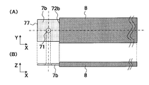
- FIG. 5 is a diagram showing an example of the shape of a scintillator 7b according to a second modification of the embodiment of the present invention
- FIG. 5 (A) is an example of a top view
- FIG. 5 (B) is an example of a side view. It is.
- the upper surface shape of the scintillator 7b is square or rectangular, and the end surface 72b of the end of the scintillator 7b in contact with the end of the light guide 8 and the scintillator 7b
- the end surface 77 at the end opposite to the end surface 72b is a plane parallel to each other and perpendicular to the X axis.
- the metal film formed as the light reflecting film is formed in the same manner as in the above-described embodiment. Then, a gap is provided between the end surface 72b of the scintillator 7b and the light guide 8, or they are joined with a joining material such as transparent resin, optical cement, or matching oil interposed.
- the electron beam detector 12 and the electron microscope 100 manufactured using the scintillator 7b as described above have good characteristics of high detection sensitivity of reflected electrons and quick response. This is because, in the second modification, the end surface 77 at the end of the scintillator 7b has an action of reflecting the fluorescence generated in the scintillator 7b to the end surface 72b on the light guide 8 side, and the scintillator 7b This is nothing but the effect based on the Y—Al—O-based ceramic sintered body using Ce as an activator.
- FIGS. 6A and 6B are diagrams showing an example of the shape of a scintillator 7c according to a third modification of the embodiment of the present invention, in which FIG. 6A is an example of a top view, and FIG. 6B is an example of a side view. It is.
- the upper surface shape of the scintillator 7c is a trapezoidal quadrilateral, and the end surface 72c of the end portion of the scintillator 7c in contact with the end portion of the light guide 8 and the scintillator 7c.
- the end surface 72c and the end surface 77 at the opposite end are parallel to each other and are perpendicular to the X axis.
- an end surface 78 and an end surface 79 that connect the end surface 72c and the end surface 77 of the scintillator 7c are inclined with respect to the X axis, and the width of the scintillator 7c in the Y direction is large on the end surface 72c side and small on the end surface 77 side. It is molded into. That is, the separation distance between the end surface 78 and the end surface 79 decreases as the distance from the end surface 72c increases. Further, the upper surface 76 of the scintillator 7c is inclined with respect to the electron incident surface 75, and the thickness of the scintillator 7c in the Z direction is thicker on the end surface 72c side and thinner on the end surface 77 side.
- the metal film formed as the light reflecting film is formed in the same manner as in the above-described embodiment. Then, a gap is provided between the end surface 72c of the scintillator 7c and the light guide 8, or a joining material such as a transparent resin, optical cement, or matching oil is interposed therebetween.
- the electron beam detector 12 and the electron microscope 100 manufactured using the scintillator 7c as described above have good characteristics of high detection sensitivity of reflected electrons and quick response. This is because, in the third modification, the electron incident surface 75, the upper surface 76, the end surface 77, the end surface 78, and the end surface 79 at the end of the scintillator 7c write the fluorescence generated in the scintillator 7c with a small number of multiple reflections. It has an effect of guiding light to the end face 72c on the guide 8 side, and is nothing but an effect based on the fact that the scintillator 7c is formed of a Y—Al—O ceramic sintered body using Ce as an activator. .
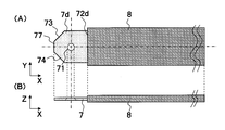
- FIGS. 7A and 7B are diagrams showing an example of the shape of a scintillator 7d according to a fourth modification of the embodiment of the present invention.
- FIG. 7A is an example of a top view
- FIG. 7B is an example of a side view. It is.
- the shape of the scintillator 7d is a combination of the shape of the scintillator 7a of the first modification and the shape of the scintillator 7b of the second modification.
- the end surface of the scintillator 7d opposite to the end surface 72d is composed of three end surfaces: an end surface 73, an end surface 74, and an end surface 77.
- the end surface 77 is formed so as to be substantially parallel to the end surface 72d, and the end surface 73 and the end surface 74 are formed to form angles ⁇ 1 and ⁇ 2 (not shown) with the X axis, respectively.
- the angles ⁇ 1 and ⁇ 2 are assumed to be 30 degrees ⁇ ⁇ 1 and ⁇ 2 ⁇ 90 degrees, as in the case of the above-described embodiment (see FIG. 3).
- the metal film formed as the light reflecting film is formed in the same manner as in the above-described embodiment. Then, a gap is provided between the end surface 72d of the scintillator 7d and the light guide 8, or a joining material such as transparent resin, optical cement, matching oil or the like is interposed therebetween.
- the electron beam detector 12 and the electron microscope 100 manufactured using the scintillator 7d as described above have good characteristics of high detection sensitivity of reflected electrons and quick response. This is because, in the fourth modification, the end surface 73, the end surface 74 and the end surface 77 at the end of the scintillator 7d have an action of reflecting the fluorescence generated in the scintillator 7d to the end surface 72d on the light guide 8 side. Furthermore, there is nothing but an effect based on the fact that the scintillator 7d is formed of a Y—Al—O-based ceramic sintered body using Ce as an activator.
- the end face 77 is formed substantially parallel to the end face 72d, but it is not necessarily required to be parallel. However, it is assumed that the angles formed by the end surface 77 and the end surface 73 and the end surface 74 are both less than 180 degrees. This means that the end surface 73, the end surface 77, and the end surface 74 are part of an outwardly convex polyhedron.
- FIG. 8 is a diagram showing an example of the shape of scintillators 7e and 7e ′ according to a fifth modification of the embodiment of the present invention
- FIG. 8A is an example of a top view
- FIG. 8B is a side view. It is an example of a figure.
- the shape of the scintillators 7e and 7e ′ according to the fifth modified example is that the scintillator 7a of the first modified example is divided into two in the vertical direction (Y direction). It has a different shape.
- the two divided scintillators 7e and 7e ' are connected to different light guides 8 and 8', respectively.
- the end surfaces 72e and 72e ′ at the ends where the scintillators 7e and 7e ′ are in contact with the light guides 8 and 8 ′, respectively, are not convex surfaces but flat surfaces. It may be a convex surface on the outside.
- the metal film formed as the light reflecting film is formed in the same manner as in the above-described embodiment, and the light reflecting metal film is also formed on the end face of the boundary between the divided scintillators 7e and 7e '. Is formed.
- gaps are provided between the end surfaces 72e and 72e ′ of the scintillators 7e and 7e ′ and the light guides 8 and 8 ′, or a bonding material such as transparent resin, optical cement, and matching oil is interposed. Are joined.
- the electron beam detector 12 and the electron microscope 100 manufactured using the scintillators 7e and 7e 'as described above have good characteristics such as high detection sensitivity of reflected electrons and quick response. This is because, in each of the scintillators 7e and 7e ′ of the fifth modified example, end surfaces 73 and 74 inclined with respect to the X axis, and upper surfaces 76 and inclined with an inclination angle ⁇ with respect to the electron incident surfaces 75 and 75 ′. 76 'has an action of reflecting the fluorescence generated in the scintillators 7e, 7e' to the end surfaces 72e, 72e 'on the light guide 8, 8' side, and the scintillators 7e, 7e 'are attached with Ce. This is nothing but the effect based on the fact that it is formed of a Y—Al—O-based ceramic sintered body as an activator.
- the two scintillators 7e and 7e ' are connected to different photoelectric conversion elements 9 (see FIG. 1) via different light guides 8 and 8', respectively.
- the electron microscope 100 according to the present modification includes two electron beam detectors 12 that are independent of each other. Therefore, the electron microscope 100 can obtain two types of observation images. For example, when the sample 5 is tilted and observed, the reflected electrons 6 are emitted in a biased manner depending on the unevenness of the surface of the sample 5. It is possible to observe the difference in the observation image based on the difference.
- the scintillator 7 is divided into two, but is not limited to two, and may be divided into three or more, such as four or six. Further, when the scintillator 7 is divided into a plurality of parts, the divided scintillators 7 and 7 ′ do not have to have a symmetrical shape.
- FIG. 9 is a diagram showing an example of the shape of the light reflecting metal film formed on the electron incident surface 75 of the scintillator 7f according to the sixth modification of the embodiment of the present invention.
- the scintillator 7f itself has the same shape as the scintillator 7 of the above-described embodiment. Therefore, an electron passage hole 71 is formed in the approximate center of the scintillator 7f.
- a metal film having a thickness that does not prevent the reflected electrons 6 from entering is formed in a region 75a in a circle concentric with the electron passage hole 71 on the electron incident surface 75, and a region 75b outside the concentric circle is formed.
- a metal film having a thickness for blocking the incidence of the reflected electrons 6 is formed.
- the other surfaces except the electron incident surface 75 of the scintillator 7f and the end surface 72 that is in contact with the light guide 8 form a metal film having a thickness that blocks the incidence of the reflected electrons 6.
- the film thickness that does not hinder the incidence of the reflected electrons 6 is 100 nm or less, preferably about 50 nm, and the film thickness that blocks the incidence of the reflected electrons 6 exceeds 100 nm.
- the film thickness is preferably about 200 nm.
- the incident of the reflected electrons 6 to the scintillator 7f is limited to the region 75a of the electron incident surface 75, so that the isotropic detection of the reflected electrons 6 is ensured.
- the shape of the electron incident surface 75 of the scintillator 7 is not rotationally symmetric, so that there is a problem that the amount of reflected electrons emitted cannot be accurately detected. In the example scintillator 7f, the problem does not occur. That is, in this modified example, in addition to the same effects as those of the above-described embodiment, the effect of enabling isotropic detection of the reflected electrons 6 is obtained.
- the present invention is not limited to the above-described embodiment and its modifications, and further includes various modifications.
- the above embodiment has been described in detail for easy understanding of the present invention, and is not necessarily limited to the one having all the configurations described.
- a part of the configuration of an embodiment or a modification can be replaced with a part of the configuration of another embodiment or a modification, and further, the configuration of another embodiment can be replaced with the configuration of another embodiment. It is also possible to add some or all.
Landscapes
- Chemical & Material Sciences (AREA)
- Analytical Chemistry (AREA)
- Measurement Of Radiation (AREA)
Abstract
Description
なお、このような発光強度のCe組成比xに対する依存特性は、10kVで加速した電子線に限らず、様々なエネルギーを有する電子線についても、ほぼ同様の傾向を示す。
図4は、本発明の実施形態の第1の変形例に係るシンチレータ7aの形状の例を示した図で、図4(A)は上面図の例、図4(B)は側面図の例である。図4(A)、(B)に示すように、シンチレータ7aの形状は、図3(A)、(B)に示したシンチレータの形状と一部を除きほとんど同じである。以下、形状が相違する部分についてのみ説明する。
図5は、本発明の実施形態の第2の変形例に係るシンチレータ7bの形状の例を示した図で、図5(A)は上面図の例、図5(B)は側面図の例である。図5(A)、(B)に示すように、シンチレータ7bの上面形状は、正方形または長方形状であり、ライトガイド8の端部に接するシンチレータ7bの端部の端面72b、および、シンチレータ7bの端面72bと反対側の端部の端面77は、互いに平行で、X軸に垂直な平面である。
図6は、本発明の実施形態の第3の変形例に係るシンチレータ7cの形状の例を示した図で、図6(A)は上面図の例、図6(B)は側面図の例である。図6(A)、(B)に示すように、シンチレータ7cの上面形状は、台形状の四辺形であり、ライトガイド8の端部に接するシンチレータ7cの端部の端面72c、および、シンチレータ7cの端面72cとその反対側の端部の端面77は、互いに平行で、X軸に垂直な平面である。また、シンチレータ7cの端面72cと端面77とをそれぞれつなぐ端面78および端面79は、X軸に対し傾斜し、シンチレータ7cのY方向の幅は、端面72c側で大きく、端面77側で小さくなるように成形されている。つまり、端面78と端面79との離間距離は、端面72cから遠ざかるに従って小さくなる。また、シンチレータ7cの上面76は、電子入射面75に対し傾斜し、シンチレータ7cのZ方向の厚さは、端面72c側で厚く、端面77側で薄くなるように成形されている。
図7は、本発明の実施形態の第4の変形例に係るシンチレータ7dの形状の例を示した図で、図7(A)は上面図の例、図7(B)は側面図の例である。図7(A)、(B)に示すように、シンチレータ7dの形状は、第1の変形例のシンチレータ7aの形状と第2の変形例のシンチレータ7bの形状とを折衷した形状となっている。すなわち、シンチレータ7dの端面72dと反対側の端部の端面は、端面73、端面74および端面77の3つの端面により構成されている。
図8は、本発明の実施形態の第5の変形例に係るシンチレータ7e,7e’の形状の例を示した図で、図8(A)は上面図の例、図8(B)は側面図の例である。図8(A)、(B)に示すように、第5の変形例に係るシンチレータ7e,7e’の形状は、第1の変形例のシンチレータ7aが、上下(Y方向)2つに分割された形状をしている。そして、分割された2つのシンチレータ7e,7e’は、それぞれ異なるライトガイド8,8’に接続されている。
図9は、本発明の実施形態の第6の変形例に係るシンチレータ7fの電子入射面75に形成する光反射用の金属膜の形状の例を示した図である。なお、シンチレータ7fそのものの形状は、前記した実施形態のシンチレータ7と同じであるとする。従って、シンチレータ7fのほぼ中央には、電子通過孔71が形成されている。
2 走査レンズ
3 対物レンズ
4 試料室
5 試料
6 反射電子
7,7a,7b,7c,7d,7e,7e’,7f シンチレータ
8,8’ ライトガイド
9 光電変換素子
10 増幅回路
12 電子線検出器
14 表示装置
71 電子通過孔
75 電子入射面
100 電子顕微鏡
Claims (13)
- 電子線の入射により蛍光を発する板状のシンチレータと、
前記シンチレータの屈折率よりも小さな屈折率を有し、前記シンチレータで発光した蛍光を導光するライトガイドと、
を備え、
前記シンチレータは、
端面の一部が外側に凸状の曲面で形成され、前記凸状の曲面の端面を介して前記ライトガイドに接合されていること
を特徴とする電子顕微鏡。 - 前記シンチレータと前記ライトガイドとは、前記シンチレータの屈折率よりも小さな屈折率を有する物質層を介して接合されていること
を特徴とする請求項1に記載の電子顕微鏡。 - 前記シンチレータの端面のうち、前記ライトガイドが接合される端面以外の端面は、平面または前記シンチレータの内側に凹状の曲面であること
を特徴とする請求項1に記載の電子顕微鏡。 - 前記シンチレータの端面のうち、前記ライトガイドが接合される端面にそれぞれ接続し、互いに対向する2つの端面の離間距離は、前記ライトガイドが接合される端面から遠ざかるに従って小さくなること
を特徴とする請求項1に記載の電子顕微鏡。 - 前記ライトガイドが接合される前記シンチレータの端面にそれぞれ接続し、互いに対向する前記シンチレータの上面および下面の離間距離は、前記ライトガイドが接合される端面から遠ざかるに従って小さくなること
を特徴とする請求項1に記載の電子顕微鏡。 - 前記シンチレータの端面のうち、前記ライトガイドが接合される端面と反対側に位置する端面は、互いに180度以下の角度を成して接続される複数の平面または前記シンチレータの内側に凹状の曲面で構成されること
を特徴とする請求項1に記載の電子顕微鏡。 - 前記シンチレータの上面および下面の表面には光反射膜が形成され、前記上面に形成される光反射膜の膜厚は、電子線の入射面となる前記下面に形成される光反射膜の膜厚よりも厚いこと
を特徴とする請求項1に記載の電子顕微鏡。 - 前記シンチレータは、複数部分に分割されており、その分割された前記シンチレータのそれぞれの部分には、それぞれ独立したライトガイドが接続されていること
を特徴とする請求項1に記載の電子顕微鏡。 - 前記シンチレータは、組成式(Ln1-xCex)3M5O12(ただし、Lnは、Y、Gd、LaおよびLuから選択される少なくとも一つの元素を表し、Mは、AlおよびGaから選択される少なくとも一つの元素を表す)で表されるY-Al-O系セラミック焼結体で形成されていること
を特徴とする請求項1に記載の電子顕微鏡。 - 前記Y-Al-O系セラミック焼結体におけるCeの組成比xは、0.002≦x≦0.025であること
を特徴とする請求項9に記載の電子顕微鏡。 - 電子線の入射により蛍光を発する板状のシンチレータを備え、
前記シンチレータは、組成式(Ln1-xCex)3M5O12(ただし、Lnは、Y、Gd、LaおよびLuから選択される少なくとも一つの元素を表し、Mは、AlおよびGaから選択される少なくとも一つの元素を表す)で表されるY-Al-O系セラミック焼結体で形成され、
前記Y-Al-O系セラミック焼結体におけるCeの組成比xは、0.002≦x≦0.025であること
を特徴とする電子顕微鏡。 - 電子線の入射により蛍光を発する板状のシンチレータと、
前記シンチレータの屈折率よりも小さな屈折率を有し、前記シンチレータで発光した蛍光を導光するライトガイドと、
を備え、
前記シンチレータは、
前記ライトガイド側の端部が外側に凸状の曲面により形成され、前記ライトガイドに、前記凸状の曲面を介して接合されていること
を特徴とする電子線検出器。 - 電子線の入射により蛍光を発する板状のシンチレータを備え、
前記シンチレータは、組成式(Ln1-xCex)3M5O12(ただし、Lnは、Y、Gd、LaおよびLuから選択される少なくとも一つの元素を表し、Mは、AlおよびGaから選択される少なくとも一つの元素を表す)で表されるY-Al-O系セラミック焼結体で形成され、
前記Y-Al-O系セラミック焼結体におけるCeの組成比xは、0.002≦x≦0.025であること
を特徴とする電子線検出器。
Priority Applications (3)
| Application Number | Priority Date | Filing Date | Title |
|---|---|---|---|
| KR1020157003786A KR101701071B1 (ko) | 2012-09-25 | 2013-08-09 | 전자 현미경 및 전자선 검출기 |
| CN201380043429.2A CN104584182B (zh) | 2012-09-25 | 2013-08-09 | 电子显微镜及电子射线检测器 |
| US14/423,081 US9355815B2 (en) | 2012-09-25 | 2013-08-09 | Electron microscope and electron beam detector |
Applications Claiming Priority (2)
| Application Number | Priority Date | Filing Date | Title |
|---|---|---|---|
| JP2012210796A JP5967538B2 (ja) | 2012-09-25 | 2012-09-25 | 電子顕微鏡および電子線検出器 |
| JP2012-210796 | 2012-09-25 |
Publications (1)
| Publication Number | Publication Date |
|---|---|
| WO2014050326A1 true WO2014050326A1 (ja) | 2014-04-03 |
Family
ID=50387740
Family Applications (1)
| Application Number | Title | Priority Date | Filing Date |
|---|---|---|---|
| PCT/JP2013/071611 Ceased WO2014050326A1 (ja) | 2012-09-25 | 2013-08-09 | 電子顕微鏡および電子線検出器 |
Country Status (6)
| Country | Link |
|---|---|
| US (1) | US9355815B2 (ja) |
| JP (1) | JP5967538B2 (ja) |
| KR (1) | KR101701071B1 (ja) |
| CN (1) | CN104584182B (ja) |
| TW (1) | TWI482193B (ja) |
| WO (1) | WO2014050326A1 (ja) |
Cited By (1)
| Publication number | Priority date | Publication date | Assignee | Title |
|---|---|---|---|---|
| WO2026053275A1 (ja) * | 2024-09-03 | 2026-03-12 | 株式会社日立ハイテク | 検出器及び測定装置 |
Families Citing this family (7)
| Publication number | Priority date | Publication date | Assignee | Title |
|---|---|---|---|---|
| JP6739207B2 (ja) | 2016-03-31 | 2020-08-12 | 株式会社日立ハイテク | 荷電粒子線装置 |
| JP6919014B2 (ja) * | 2016-03-31 | 2021-08-11 | 株式会社日立ハイテク | 荷電粒子線装置 |
| WO2018173242A1 (ja) | 2017-03-24 | 2018-09-27 | 株式会社 日立ハイテクノロジーズ | 荷電粒子線装置 |
| US11239048B2 (en) * | 2020-03-09 | 2022-02-01 | Kla Corporation | Arrayed column detector |
| US12555737B2 (en) * | 2020-07-07 | 2026-02-17 | Hitachi High-Tech Corporation | Charged particle beam device |
| JP7076021B1 (ja) * | 2021-03-10 | 2022-05-26 | 浜松ホトニクス株式会社 | ライトガイド、電子線検出器、及び荷電粒子装置 |
| FR3144432A1 (fr) * | 2022-12-22 | 2024-06-28 | Centre National De La Recherche Scientifique | Dispositif d’émission de lumière avec une extraction améliorée |
Citations (5)
| Publication number | Priority date | Publication date | Assignee | Title |
|---|---|---|---|---|
| JPH02118485A (ja) * | 1988-10-28 | 1990-05-02 | Hamamatsu Photonics Kk | 放射線検出器 |
| JPH11273608A (ja) * | 1998-03-23 | 1999-10-08 | Hitachi Ltd | 走査電子顕微鏡 |
| JP2012500447A (ja) * | 2008-08-20 | 2012-01-05 | 株式会社アドバンテスト | 電子検出装置及び走査型電子顕微鏡 |
| JP2012013460A (ja) * | 2010-06-29 | 2012-01-19 | Horiba Ltd | 放射線検出器 |
| JP2012180399A (ja) * | 2011-02-28 | 2012-09-20 | Furukawa Co Ltd | シンチレータ用ガーネット型結晶、及び、これを用いる放射線検出器 |
Family Cites Families (17)
| Publication number | Priority date | Publication date | Assignee | Title |
|---|---|---|---|---|
| JPS5418269A (en) * | 1977-07-11 | 1979-02-10 | Jeol Ltd | Electron beam detector |
| WO1984000443A1 (en) * | 1982-07-16 | 1984-02-02 | Lintech Instr Ltd | Electron beam apparatus and electron collectors therefor |
| JPS59197881A (ja) | 1983-04-25 | 1984-11-09 | Jeol Ltd | エネルギ−選択機能を有する反射電子検出装置 |
| DE3500903A1 (de) | 1985-01-12 | 1986-07-17 | Fa. Carl Zeiss, 7920 Heidenheim | Detektor fuer rueckstreuelektronen |
| JP3730263B2 (ja) * | 1992-05-27 | 2005-12-21 | ケーエルエー・インストルメンツ・コーポレーション | 荷電粒子ビームを用いた自動基板検査の装置及び方法 |
| JPH07122220A (ja) * | 1993-10-21 | 1995-05-12 | Hitachi Ltd | 電子顕微鏡装置 |
| US5635720A (en) * | 1995-10-03 | 1997-06-03 | Gatan, Inc. | Resolution-enhancement device for an optically-coupled image sensor for an electron microscope |
| US5982190A (en) * | 1998-02-04 | 1999-11-09 | Toro-Lira; Guillermo L. | Method to determine pixel condition on flat panel displays using an electron beam |
| US6642520B2 (en) | 1999-04-13 | 2003-11-04 | Kabushiki Kaisha Topcon | Scanning electron microscope |
| JP2000299078A (ja) | 1999-04-13 | 2000-10-24 | Topcon Corp | 走査型電子顕微鏡 |
| US6855929B2 (en) * | 2000-12-01 | 2005-02-15 | Ebara Corporation | Apparatus for inspection with electron beam, method for operating same, and method for manufacturing semiconductor device using former |
| JP2003031173A (ja) * | 2001-07-11 | 2003-01-31 | Ebara Corp | 荷電粒子ビーム制御装置及びそれを用いた荷電粒子ビーム光学装置、ならびに荷電粒子ビーム欠陥検査装置 |
| JP2004363085A (ja) * | 2003-05-09 | 2004-12-24 | Ebara Corp | 荷電粒子線による検査装置及びその検査装置を用いたデバイス製造方法 |
| JP5352262B2 (ja) * | 2009-02-06 | 2013-11-27 | 株式会社日立ハイテクノロジーズ | 荷電粒子線装置 |
| JP5818542B2 (ja) * | 2010-07-29 | 2015-11-18 | 浜松ホトニクス株式会社 | イオン検出装置 |
| US8895935B2 (en) * | 2012-03-12 | 2014-11-25 | Hermes Microvision, Inc. | High efficiency secondary and back scattered electron detector |
| US8829451B2 (en) * | 2012-06-13 | 2014-09-09 | Hermes Microvision, Inc. | High efficiency scintillator detector for charged particle detection |
-
2012
- 2012-09-25 JP JP2012210796A patent/JP5967538B2/ja not_active Expired - Fee Related
-
2013
- 2013-07-23 TW TW102126278A patent/TWI482193B/zh not_active IP Right Cessation
- 2013-08-09 US US14/423,081 patent/US9355815B2/en not_active Expired - Fee Related
- 2013-08-09 WO PCT/JP2013/071611 patent/WO2014050326A1/ja not_active Ceased
- 2013-08-09 CN CN201380043429.2A patent/CN104584182B/zh not_active Expired - Fee Related
- 2013-08-09 KR KR1020157003786A patent/KR101701071B1/ko not_active Expired - Fee Related
Patent Citations (5)
| Publication number | Priority date | Publication date | Assignee | Title |
|---|---|---|---|---|
| JPH02118485A (ja) * | 1988-10-28 | 1990-05-02 | Hamamatsu Photonics Kk | 放射線検出器 |
| JPH11273608A (ja) * | 1998-03-23 | 1999-10-08 | Hitachi Ltd | 走査電子顕微鏡 |
| JP2012500447A (ja) * | 2008-08-20 | 2012-01-05 | 株式会社アドバンテスト | 電子検出装置及び走査型電子顕微鏡 |
| JP2012013460A (ja) * | 2010-06-29 | 2012-01-19 | Horiba Ltd | 放射線検出器 |
| JP2012180399A (ja) * | 2011-02-28 | 2012-09-20 | Furukawa Co Ltd | シンチレータ用ガーネット型結晶、及び、これを用いる放射線検出器 |
Cited By (1)
| Publication number | Priority date | Publication date | Assignee | Title |
|---|---|---|---|---|
| WO2026053275A1 (ja) * | 2024-09-03 | 2026-03-12 | 株式会社日立ハイテク | 検出器及び測定装置 |
Also Published As
| Publication number | Publication date |
|---|---|
| KR101701071B1 (ko) | 2017-01-31 |
| CN104584182B (zh) | 2016-12-28 |
| CN104584182A (zh) | 2015-04-29 |
| US9355815B2 (en) | 2016-05-31 |
| TW201419363A (zh) | 2014-05-16 |
| JP2014067526A (ja) | 2014-04-17 |
| JP5967538B2 (ja) | 2016-08-10 |
| US20150214002A1 (en) | 2015-07-30 |
| TWI482193B (zh) | 2015-04-21 |
| KR20150036579A (ko) | 2015-04-07 |
Similar Documents
| Publication | Publication Date | Title |
|---|---|---|
| JP5967538B2 (ja) | 電子顕微鏡および電子線検出器 | |
| TWI455169B (zh) | 帶電粒子偵測裝置 | |
| US11694873B2 (en) | Charged particle beam apparatus | |
| CN1886675B (zh) | 彩色闪烁器和图像传感器 | |
| JP6101443B2 (ja) | シンチレータ及びこれを用いた放射線検出器 | |
| JP6087421B2 (ja) | シンチレータ及び放射線検出器 | |
| WO2015185995A1 (ja) | 荷電粒子線装置 | |
| CN105849591B (zh) | 辐射探测器和闪烁体板、以及其制造方法 | |
| JP2012058170A (ja) | シンチレータパネル | |
| JP2000155219A (ja) | 集光器 | |
| JP7140902B2 (ja) | 荷電粒子線装置 | |
| US12339407B2 (en) | Device for detecting charged particles or radiation | |
| US12512295B2 (en) | Light guide, electron ray detector, and charged particle device | |
| CN110455835A (zh) | 一种软x射线显微成像探测器 | |
| WO2013168488A1 (ja) | 荷電粒子線顕微鏡 | |
| WO2026053275A1 (ja) | 検出器及び測定装置 | |
| TW202611964A (zh) | 偵測器及測定裝置 | |
| CN120530474A (zh) | 检测器、测量装置以及带电粒子束装置 | |
| US9798018B2 (en) | Luminescent beam stop | |
| CS269916B1 (cs) | Monokrystalioký eointilátor pro detekci sekundárních elektronů |
Legal Events
| Date | Code | Title | Description |
|---|---|---|---|
| 121 | Ep: the epo has been informed by wipo that ep was designated in this application |
Ref document number: 13841585 Country of ref document: EP Kind code of ref document: A1 |
|
| ENP | Entry into the national phase |
Ref document number: 20157003786 Country of ref document: KR Kind code of ref document: A |
|
| WWE | Wipo information: entry into national phase |
Ref document number: 14423081 Country of ref document: US |
|
| NENP | Non-entry into the national phase |
Ref country code: DE |
|
| 122 | Ep: pct application non-entry in european phase |
Ref document number: 13841585 Country of ref document: EP Kind code of ref document: A1 |