WO2014045846A1 - 静電容量型入力装置の製造方法および静電容量型入力装置、並びに、これを備えた画像表示装置 - Google Patents
静電容量型入力装置の製造方法および静電容量型入力装置、並びに、これを備えた画像表示装置 Download PDFInfo
- Publication number
- WO2014045846A1 WO2014045846A1 PCT/JP2013/073412 JP2013073412W WO2014045846A1 WO 2014045846 A1 WO2014045846 A1 WO 2014045846A1 JP 2013073412 W JP2013073412 W JP 2013073412W WO 2014045846 A1 WO2014045846 A1 WO 2014045846A1
- Authority
- WO
- WIPO (PCT)
- Prior art keywords
- layer
- transparent electrode
- electrode pattern
- input device
- front plate
- Prior art date
- Legal status (The legal status is an assumption and is not a legal conclusion. Google has not performed a legal analysis and makes no representation as to the accuracy of the status listed.)
- Ceased
Links
Images




Classifications
-
- G—PHYSICS
- G06—COMPUTING OR CALCULATING; COUNTING
- G06F—ELECTRIC DIGITAL DATA PROCESSING
- G06F3/00—Input arrangements for transferring data to be processed into a form capable of being handled by the computer; Output arrangements for transferring data from processing unit to output unit, e.g. interface arrangements
- G06F3/01—Input arrangements or combined input and output arrangements for interaction between user and computer
- G06F3/03—Arrangements for converting the position or the displacement of a member into a coded form
- G06F3/041—Digitisers, e.g. for touch screens or touch pads, characterised by the transducing means
- G06F3/044—Digitisers, e.g. for touch screens or touch pads, characterised by the transducing means by capacitive means
- G06F3/0443—Digitisers, e.g. for touch screens or touch pads, characterised by the transducing means by capacitive means using a single layer of sensing electrodes
-
- G—PHYSICS
- G06—COMPUTING OR CALCULATING; COUNTING
- G06F—ELECTRIC DIGITAL DATA PROCESSING
- G06F3/00—Input arrangements for transferring data to be processed into a form capable of being handled by the computer; Output arrangements for transferring data from processing unit to output unit, e.g. interface arrangements
- G06F3/01—Input arrangements or combined input and output arrangements for interaction between user and computer
- G06F3/03—Arrangements for converting the position or the displacement of a member into a coded form
- G06F3/041—Digitisers, e.g. for touch screens or touch pads, characterised by the transducing means
- G06F3/044—Digitisers, e.g. for touch screens or touch pads, characterised by the transducing means by capacitive means
-
- G—PHYSICS
- G06—COMPUTING OR CALCULATING; COUNTING
- G06F—ELECTRIC DIGITAL DATA PROCESSING
- G06F3/00—Input arrangements for transferring data to be processed into a form capable of being handled by the computer; Output arrangements for transferring data from processing unit to output unit, e.g. interface arrangements
- G06F3/01—Input arrangements or combined input and output arrangements for interaction between user and computer
- G06F3/03—Arrangements for converting the position or the displacement of a member into a coded form
- G06F3/041—Digitisers, e.g. for touch screens or touch pads, characterised by the transducing means
- G06F3/044—Digitisers, e.g. for touch screens or touch pads, characterised by the transducing means by capacitive means
- G06F3/0446—Digitisers, e.g. for touch screens or touch pads, characterised by the transducing means by capacitive means using a grid-like structure of electrodes in at least two directions, e.g. using row and column electrodes
-
- G—PHYSICS
- G06—COMPUTING OR CALCULATING; COUNTING
- G06F—ELECTRIC DIGITAL DATA PROCESSING
- G06F2203/00—Indexing scheme relating to G06F3/00 - G06F3/048
- G06F2203/041—Indexing scheme relating to G06F3/041 - G06F3/045
- G06F2203/04103—Manufacturing, i.e. details related to manufacturing processes specially suited for touch sensitive devices
-
- G—PHYSICS
- G06—COMPUTING OR CALCULATING; COUNTING
- G06F—ELECTRIC DIGITAL DATA PROCESSING
- G06F2203/00—Indexing scheme relating to G06F3/00 - G06F3/048
- G06F2203/041—Indexing scheme relating to G06F3/041 - G06F3/045
- G06F2203/04111—Cross over in capacitive digitiser, i.e. details of structures for connecting electrodes of the sensing pattern where the connections cross each other, e.g. bridge structures comprising an insulating layer, or vias through substrate
Definitions
- the present invention relates to a decorative transfer film for manufacturing a capacitive input device capable of detecting a contact position of a finger as a change in capacitance, a method for manufacturing a capacitive input device, and a method for manufacturing the same.
- the present invention relates to an obtained capacitive input device and an image display device including the capacitive input device as a constituent element.
- Such input devices include a resistance film type and a capacitance type.
- the resistance film type input device has a drawback that it has a narrow operating temperature range and is susceptible to changes over time because it has a two-layer structure of film and glass that is shorted by pressing the film.
- the capacitance-type input device has an advantage that a light-transmitting conductive film is simply formed on a single substrate.
- electrode patterns are extended in directions intersecting each other, and when a finger or the like comes into contact, the capacitance between the electrodes is detected to detect the input position.
- an electrostatic capacitance type input device an alternating current of the same phase and the same potential is applied to both ends of the translucent conductive film to detect a weak current flowing when a capacitor is formed in contact with or close to a finger.
- Some types detect the input position.
- a capacitive input device a plurality of first transparent electrode patterns and a plurality of first transparent electrode patterns formed by extending a plurality of pad portions in a first direction via connecting portions. And a plurality of second transparent electrode patterns comprising a plurality of pad portions formed to extend in a direction crossing the first direction and electrically insulated via an interlayer insulating layer An input device is disclosed (for example, see Patent Document 2 below).
- the capacitance type input device has a front plate laminated on the produced capacitance type input device, there is a problem that the capacitance type input device becomes thick and heavy.
- a capacitive touch panel in which a mask layer, a sense circuit, and an interlayer insulating layer are integrally formed on the non-contact side surface of the front plate is disclosed (for example, see Patent Document 3 below).
- Patent Document 3 since the capacitive touch panel has a front plate integrated with the capacitive input device, it is possible to reduce the thickness / weight and further mask the sense circuit with a mask layer. The appearance of the device was improved.
- JP 2007-122326 A Japanese Patent No. 4506785 JP 2009-193587 A JP 2011-218561 A JP 2008-169237 A JP 2011-197220 A
- Patent Document 3 only describes that the mask layer may be formed of a black resin or other opaque coating material, but various color tones (between the mask layer and the front plate as required). Black, white, pastel colors, metallic, etc.) can be provided, and in recent years, it has been particularly demanded to increase the brightness and whiteness of the white decorative layer.
- a method of providing this decoration layer conventionally, a method using liquid resist coating, screen printing, or the like has been the mainstream.
- tempered glass typified by Corning Gorilla Glass (registered trademark) is used for the front plate (the surface directly touched by a finger).
- a liquid resist or a screen printing ink having a low hiding power is used.
- a decorative layer on tempered glass when heated in a process for producing a circuit such as a transparent conductive layer, there is a problem that the whiteness decreases.
- a white film having high heat resistance at least (A) a thermosetting resin substantially free of silicon in the molecule and (B) a white thermosetting resin composition containing a white colorant.
- a multilayer film is proposed in which a layer to be formed is provided on at least one side of a polyimide film (see, for example, Patent Document 4).
- Patent Document 4 this also has a problem that the whiteness is lowered when heated at a high temperature in a process for producing a circuit such as a transparent conductive layer.
- a white polyimide film obtained by imidizing a polyimide precursor film obtained by mixing a white pigment with a polyamic acid obtained by reacting diamine and aromatic tetracarboxylic acid has been proposed.
- this also has a problem that the whiteness is lowered when heated at a high temperature in a process for producing a circuit such as a transparent conductive layer.
- a light diffusing reflective film in which at least a light diffusing layer containing a resin and transparent fine particles and a metal reflecting layer are sequentially formed on one surface of a plastic film has been proposed (for example, And Patent Document 6).
- the resin and transparent fine particles used in this light diffusive reflective film have low heat resistance, and similarly, when heated at a high temperature in a process for producing a circuit such as a transparent conductive layer, the degree of whiteness decreases.
- the present inventors have studied, when a thin white decorative layer is formed by the method described in these documents, it is not possible to obtain a performance satisfying the brightness and whiteness after transfer. I understood it. Moreover, it turned out that it is difficult to obtain the white decorating layer which satisfies the said characteristic with high yield.
- the problem to be solved by the present invention is to obtain a white decorative layer having good brightness and whiteness even if it is a thin layer with a high yield, and a capacitive / input device that is thin / lightweight.
- the object is to provide an image display device used.
- the reflective layer with a specific composition in the decorative layer, even if it is a thin layer, brightness and whiteness Can be obtained with a high yield, and the short circuit of the metal wiring when a reflective layer having a specific composition is introduced can be eliminated by providing an insulating mask layer. It has been found that the layer / weight can be reduced, and that the capacitive input device can be manufactured with high quality in a simple process.
- Mask layer [2] The electrostatic capacity described in [1] In the method for manufacturing a capacitive input device, the reflective layer is preferably made of metal.
- the thickness of the reflective layer is preferably 100 nm or more.
- the method for manufacturing a capacitive input device according to any one of [1] to [3] it is preferable that at least (1) is formed using a transfer film having a colored layer.
- the method for manufacturing a capacitance-type input device according to any one of [1] to [4] includes (1) an environment of 0.08 to 1.2 atm after the decorative layer is laminated. It is preferable to include a step of heating to 110 to 300 ° C. below.
- the method for manufacturing a capacitive input device according to any one of [1] to [5] includes the following elements (4) to (6) on the element (3): It is preferable to laminate.
- the capacitive input device further includes (7) the first transparent electrode pattern and It is preferable to have a conductive element that is electrically connected to at least one of the second electrode patterns and is different from the first transparent electrode pattern and the second electrode pattern.
- (7) another conductive element may be installed at least on the surface side opposite to the front plate of the mask layer. preferable.
- the method for manufacturing a capacitive input device according to [10] or [11] further includes (8) transparent so as to cover all or part of the elements (1) to (7). It is preferable to install a protective layer.
- the method for manufacturing a capacitive input device uses a transfer film having the transparent protective layer and a temporary support, a thermoplastic resin layer, and a photocurable resin layer in this order. It is preferable that the photocurable resin layer of the transfer film is transferred and formed.
- the method of manufacturing a capacitive input device according to any one of [10] to [13] includes at least one of the first transparent electrode pattern, the second electrode pattern, and the conductive element. One is preferably formed by etching the transparent conductive material using an etching pattern formed by a transfer film having a temporary support, a thermoplastic resin layer, and a photocurable resin layer in this order.
- [15] The method for manufacturing a capacitive input device according to any one of [10] to [14], wherein at least one of the first transparent electrode pattern, the second electrode pattern, and the conductive element is provided.
- One is to transfer and form the conductive photocurable resin layer of the transfer film using a transfer film having a temporary support, a thermoplastic resin layer, and a conductive photocurable resin layer in this order. Is preferred.
- [16] The method for manufacturing a capacitive input device according to any one of [1] to [15], wherein the non-contact surface of the front plate is subjected to a surface treatment, and the surface treatment is performed before the surface treatment. It is preferable to install a decorative layer on the non-contact surface of the face plate.
- a silane compound is preferably used for the surface treatment of the front plate.
- the front plate has an opening at least partially.
- An image display device comprising the capacitive input device according to [19] as a constituent element.
- the decorative layer by providing the decorative layer with a laminate of metal or inorganic layer, a decorative layer with good brightness and whiteness can be obtained with a high yield even if it is a thin layer.
- an insulating mask layer By installing an insulating mask layer, it is possible to eliminate the short circuit of metal wiring when introducing a laminated body of metal or inorganic layer, and a capacitive / input device that is thin / lightweight can be manufactured in a simple process with high quality.
- a capacitive input device manufacturing method that can be manufactured at the same time, a capacitive input device obtained by the manufacturing method, and an image display device using the capacitive input device are provided. be able to.
- a method for manufacturing a capacitance-type input device of the present invention includes a front plate and at least the following elements (1) to (3) on the non-contact side of the front plate.
- the (1), (2), and (3) are stacked in this order on the non-contact side of the front plate.
- the manufacturing method comprises a layer of an inorganic layer or a reflective layer made of metal (hereinafter referred to as a layer of metal or inorganic layer) on the surface opposite to the front plate on the decorative layer on the non-contact side of the front plate. If the decorative layer is a thin layer, sufficient brightness and whiteness can be obtained. Further, by providing a mask layer on the surface of the laminated body of the metal or inorganic layer opposite to the decorative layer, it is possible to prevent a short circuit due to the laminated body of the metal or inorganic layer.
- an adhesion-imparting layer is provided between the laminate of the metal or inorganic layer and the decorative layer, and an adhesion-imparting layer and a barrier layer are provided on the metal or inorganic layer laminate and the mask layer side from the viewpoint of storage stability.
- an adhesion-imparting layer and a barrier layer are provided on the metal or inorganic layer laminate and the mask layer side from the viewpoint of storage stability.
- FIG. 1 is a cross-sectional view showing a preferred configuration of the capacitance-type input device of the present invention.
- a capacitive input device 10 includes a front plate 1, a decorative layer 2a, a reflective layer (a laminate of inorganic layers or a laminate of metals) 2b, a mask layer 2c, and a first transparent
- the electrode pattern 3, the second transparent electrode pattern 4, the insulating layer 5, the conductive element 6, and the transparent protective layer 7 are configured.
- the front plate 1 is composed of a light-transmitting substrate such as a glass substrate, and tempered glass represented by Corning's gorilla glass can be used. Moreover, in FIG. 1, the side in which each element of the front layer 1 is provided is called the non-contact surface 1a. In the capacitive input device 10 of the present invention, input is performed by bringing a finger or the like into contact with the contact surface of the front plate 1 (the surface opposite to the non-contact surface 1a).
- the front plate may be referred to as a “base material”.
- a reflective layer 2b and a mask layer 2c made of a laminate of inorganic layers or metal are provided on the non-contact surface of the front plate 1 via a decorative layer 2a.
- the reflective layer 2b made of a laminate of inorganic layers or metal can be used in combination with the decorative layer 2a to satisfy the brightness and whiteness of the decorative layer 2a.
- the mask layer 2c is a frame-like pattern around the display area formed on the non-contact side of the touch panel front plate, and is formed so as to prevent the lead wiring and the like from being seen.
- the decorative layer 2a is formed for the purpose of decoration on the reflective layer 2b made of a laminate of inorganic layers or metal, on the non-contact side of the touch panel front plate and the reflective layer 2b. As shown in FIG.
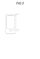
- the capacitance-type input device 10 of the present invention includes a decorative layer 2a, an inorganic layer so as to cover a part of the front plate 1 (a region other than the input surface in FIG. 2). It is preferable that a reflective layer 2b and a mask layer 2c made of a laminated body or metal are provided. Further, the front plate 1 can be provided with an opening 8 in a part of the front plate as shown in FIG. A mechanical switch by pressing can be installed in the opening 8. Since the tempered glass used as a base material has high strength and is difficult to process, it is general to form the opening 8 by forming the opening 8 before the tempering treatment and then performing the tempering treatment. .
- first transparent electrode patterns 3 formed by extending a plurality of pad portions in the first direction via connection portions, and a first transparent electrode pattern 3 And a plurality of second transparent electrode patterns 4 comprising a plurality of pad portions formed extending in a direction crossing the first direction, the first transparent electrode pattern 3 and the second And an insulating layer 5 that electrically insulates the transparent electrode pattern 4.
- the first transparent electrode pattern 3, the second transparent electrode pattern 4, and the conductive element 6 described later are, for example, ITO (Indium It can be made of a light-transmitting conductive metal oxide film such as Tin Oxide) or IZO (Indium Zinc Oxide).
- metal films examples include ITO films; metal films such as Al, Zn, Cu, Fe, Ni, Cr, and Mo; metal oxide films such as SiO 2 .
- the film thickness of each element can be set to 10 to 200 nm.
- the amorphous ITO film is made into a polycrystalline ITO film by firing, the electrical resistance can be reduced.
- said 1st transparent electrode pattern 3, the 2nd transparent electrode pattern 4, and the electroconductive element 6 mentioned later are the transfer films which have the electroconductive photocurable resin layer using the below-mentioned electroconductive fiber. It can also be manufactured by transferring the conductive photocurable resin layer of the transfer film.
- paragraphs [0014] to [0016] of Japanese Patent No. 4506785 can be referred to.
- At least one of the first transparent electrode pattern 3 and the second transparent electrode pattern 4 extends over both regions of the non-contact surface of the front plate 1 and the surface opposite to the front plate 1 of the mask layer 2c.
- FIG. 1 a diagram is shown in which the second transparent electrode pattern is installed across both areas of the non-contact surface of the front plate 1 and the surface of the mask layer 2 c opposite to the front plate 1. Yes.
- expensive equipment such as a vacuum laminator is not used.
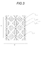
- FIG. 3 is an explanatory diagram showing an example of the first transparent electrode pattern and the second transparent electrode pattern in the present invention.
- the first transparent electrode pattern 3 is formed such that the pad portion 3a extends in the first direction via the connection portion 3b.
- the second transparent electrode pattern 4 is electrically insulated by the first transparent electrode pattern 3 and the insulating layer 5 and extends in a direction intersecting the first direction (second direction in FIG. 3). It is constituted by a plurality of pad portions that are formed.
- the pad portion 3a and the connection portion 3b may be manufactured as one body, or only the connection portion 3b is manufactured and the pad portion 3a and the second portion 3b are formed.
- the transparent electrode pattern 4 may be integrally formed (patterned).
- the pad portion 3a and the second transparent electrode pattern 4 are produced (patterned) as a single body (patterning), as shown in FIG. 3, a part of the connection portion 3b and a part of the pad portion 3a are coupled, and an insulating layer Each layer is formed so that the first transparent electrode pattern 3 and the second transparent electrode pattern 4 are electrically insulated by 5.
- a conductive element 6 is provided on the surface of the mask layer 2c opposite to the front plate 1.
- the conductive element 6 is electrically connected to at least one of the first transparent electrode pattern 3 and the second transparent electrode pattern 4, and is different from the first transparent electrode pattern 3 and the second transparent electrode pattern 4. Is another element.
- FIG. 1 a view in which the conductive element 6 is connected to the second transparent electrode pattern 4 is shown.
- the transparent protective layer 7 is installed so that all of each component may be covered.
- the transparent protective layer 7 may be configured to cover only a part of each component.
- the insulating layer 5 and the transparent protective layer 7 may be made of the same material or different materials.
- the material constituting the insulating layer 5 and the transparent protective layer 7 is preferably a material having high surface hardness and high heat resistance, and a known photosensitive siloxane resin material, acrylic resin material, or the like is used.
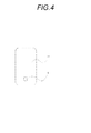
- FIG. 4 is a top view illustrating an example of the tempered glass 11 in which the opening 8 is formed.
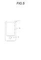
- FIG. 5 is a top view showing an example of a front plate on which a decorative layer 2a, a laminate of inorganic layers or a reflective layer 2b made of metal, and a mask layer 2c are formed.
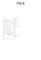
- FIG. 6 is a top view showing an example of the front plate on which the first transparent electrode pattern 3 is formed.
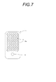
- FIG. 7 is a top view showing an example of a front plate on which the first transparent electrode pattern 3 and the second transparent electrode pattern 4 are formed.
- FIG. 8 is a top view showing an example of a front plate on which conductive elements 6 different from the first and second transparent electrode patterns are formed.
- the production method of the present invention includes a step of forming a decorative layer having a thickness of 1 ⁇ m or more and less than 30 ⁇ m on the non-contact side of the front plate, including the (1) inorganic white pigment and binder.
- the thickness of the decorative layer is preferably 1 ⁇ m or more and less than 30 ⁇ m from the viewpoint of thinning, and is preferably 1 to 25 ⁇ m from the viewpoint of increasing the hiding power of the decorative layer, and is 1.5 to 20 ⁇ m. Is particularly preferably 1.8 to 18 ⁇ m, more preferably 1.8 to 13 ⁇ m.
- the decorative layer formed by the production method of the present invention can be produced using a coloring composition, and preferably contains at least a white inorganic pigment and a binder.
- a coloring composition preferably contains at least a white inorganic pigment and a binder.
- a formation method of said (1) decoration layer For example, you may apply
- screen printing A well-known method can be used, For example, the method of patent 4021925 etc. can be used. Further, by performing screen printing a plurality of times, the film thickness can be increased even by screen printing.
- the decorating layer (1) In the production method of the present invention, it is preferable to form at least the decorating layer (1) using a transfer film.
- the method for forming the (1) decorative layer by transferring it using a transfer film will be described later.
- the thickness of the decorative layer (1) in the present invention means the total thickness of all layers.
- the decorative layer 2a and the mask layer 2c described later shown in FIG. When a transfer film having a curable resin layer is used, a substrate (front plate) having an opening has no resist component leakage from the opening, and it is necessary to form a light-shielding pattern especially to the border of the front plate. Since there is no protrusion of the resist component from the glass edge in the decoration layer or the mask layer, it is possible to manufacture a touch panel having a merit of thin layer / light weight by a simple process without contaminating the back side of the substrate.
- the transfer film that can be used in the production method of the present invention preferably has a temporary support and a colored layer, and the colored layer contains at least a white inorganic pigment and a binder.
- the transfer film that can be used in the production method of the present invention preferably has a temporary support and a colored layer. Further, a thermoplastic resin layer may be provided between the temporary support and the colored layer.
- a material that is flexible and does not cause significant deformation, shrinkage, or elongation under pressure or under pressure and heating can be used.
- a support include a polyethylene terephthalate film, a cellulose triacetate film, a polystyrene film, and a polycarbonate film, and among them, a biaxially stretched polyethylene terephthalate film is particularly preferable.
- the thickness of the temporary support is not particularly limited and is generally in the range of 5 to 200 ⁇ m, and in the range of easy handling and versatility, the range of 10 to 150 ⁇ m is particularly preferable.
- the temporary support may be transparent or may contain dyed silicon, alumina sol, chromium salt, zirconium salt or the like. Further, the temporary support can be imparted with conductivity by the method described in JP-A-2005-221726.
- the white inorganic pigment used in the colored layer includes titanium oxide (rutile type), titanium oxide (anatase type), zinc oxide, lithopone, light calcium carbonate, white carbon, aluminum oxide, aluminum hydroxide, and barium sulfate.
- titanium oxide (rutile type), titanium oxide (anatase type) and zinc oxide are more preferable, titanium oxide (rutile type) and titanium oxide (anatase type) are more preferable, and rutile type titanium oxide is still more preferable.
- titanium dioxide examples include JR, JRNC, JR-301, 403, 405, 600A, 605, 600E, 603, 701, 800, 805, 806, JA-1, C, 3, 4, 5, MT- 01, 02, 03, 04, 05, 100AQ, 100SA, 100SAK, 100SAS, 100TV, 100Z, 100ZR, 150W, 500B, 500H, 500SA, 500SAK, 500SAS, 500T, SMT-100SAM, 100SAS, 500SAM, 500SAS Manufactured), CR-50, 50-2, 57, 58, 58-2, 60, 60-2, 63, 67, 80, 85, 90, 90-2, 93, 95, 97, 953, Super70, PC -3, PF-690, 691, 711, 736, 737, 739, 740, 42, R-550, 580, 630, 670, 680, 780, 780-2, 820, 830, 850, 855, 930, 980, S
- the surface of the white inorganic pigment can be used in combination with silica treatment, alumina treatment, titania treatment, zirconia treatment, organic matter treatment and the like.
- the catalytic activity of the white inorganic pigment can be suppressed, and heat resistance, fluorescence, etc. can be improved.
- the white pigment is preferably a rutile type titanium oxide surface-treated with an inorganic substance, and at least one of alumina treatment and zirconia treatment was surface-treated.
- a rutile type titanium oxide is more preferable, and a rutile type titanium oxide surface-treated by an alumina / zirconia combined treatment is particularly preferable.
- the white inorganic pigment is contained in the total solid content of the decorative layer from the viewpoint of sufficiently shortening the development time.
- the rate is preferably 20 to 75% by mass.
- the content of the white inorganic pigment with respect to the total solid content of the colored layer is more preferably 25 to 60% by mass, and further preferably 30 to 50% by mass.
- the total solid content as used in this specification means the total mass of the non-volatile component except the solvent etc. from the said colored layer.
- the white inorganic pigment (which is the same for other colorants used in the mask layer described later) is desirably used as a dispersion.
- This dispersion can be prepared by adding and dispersing a composition obtained by previously mixing the white inorganic pigment and the pigment dispersant in an organic solvent (or vehicle) described later.
- the vehicle is a portion of a medium in which a pigment is dispersed when the paint is in a liquid state, and is a liquid component that binds to the pigment to form a coating film (binder) and dissolves and dilutes it.
- Component (organic solvent) is a portion of a medium in which a pigment is dispersed when the paint is in a liquid state, and is a liquid component that binds to the pigment to form a coating film (binder) and dissolves and dilutes it.
- the dispersing machine used for dispersing the white inorganic pigment is not particularly limited, and is described in, for example, Asakura Kunizo, “Encyclopedia of Pigments”, first edition, Asakura Shoten, 2000, item 438.
- Known dispersing machines such as a kneader, a roll mill, an atrider, a super mill, a dissolver, a homomixer, and a sand mill can be used. Further, fine grinding may be performed using frictional force by mechanical grinding described on page 310 of the document.
- the white inorganic pigment as the white inorganic pigment (coloring agent for decorative layer formation) used in the present invention has an average primary particle diameter of 0.16 ⁇ m to 0.3 ⁇ m from the viewpoint of dispersion stability and hiding power. More preferably, 0.18 ⁇ m to 0.27 ⁇ m is preferable. Further, those with 0.19 ⁇ m to 0.25 ⁇ m are particularly preferable.
- the average particle size of the primary particles is 0.16 ⁇ m, the hiding power is suddenly lowered, and the base of the mask layer may be easily seen or the viscosity may be increased.
- it exceeds 0.3 ⁇ m the whiteness is lowered, and simultaneously the hiding power is suddenly lowered, and the surface condition when applied is deteriorated.
- the “average particle size of primary particles” as used herein refers to the diameter when the electron micrograph image of the particles is a circle of the same area, and the “number average particle size” refers to the above-mentioned particle size for many particles. The diameter is obtained and the average value of the 100 is referred to.
- laser scattering HORIBA H made by Horiba Advanced Techno Co., Ltd.
- a known binder can be used as the binder of the colored layer.
- a saponified product of ethylene and an acrylate copolymer a saponified product of styrene and a (meth) acrylate copolymer, a saponified product of vinyltoluene and a (meth) acrylate copolymer, poly ( It is preferably at least one selected from (meth) acrylic acid esters, saponified products such as (meth) acrylic acid ester copolymers of butyl (meth) acrylate and vinyl acetate, and the like.
- thermoplastic resins those having a softening point of 80 ° C. or less are preferable.
- (meth) acrylic acid is a generic term for acrylic acid and methacrylic acid, and the same applies to derivatives thereof.
- an alkali-soluble resin is effective, and paragraphs [0025] of JP2011-95716A and paragraphs [0033] to [0052] of JP2010-237589A.
- the polymer described in the above can be used.
- a fluorine resin and a silicone resin are preferred. A well-known thing can be used as said silicone resin.
- a methyl-based straight silicone resin for example, a methyl-based straight silicone resin, a methylphenyl-based straight silicone resin, an acrylic resin-modified silicone resin, a polyester resin-modified silicone resin, an epoxy resin-modified silicone resin, an alkyd resin, a modified silicone resin, and a rubber-based silicone resin can be used.
- the colored layer does not necessarily require photocuring by a combination of a photocurable resin and a photopolymerization initiator, and the colored layer contains a photocurable resin or a photopolymerization initiator. May or may not be included.
- the (B) silicone resin is preferably thermosetting. More preferred are methyl straight silicone resin, methylphenyl straight silicone resin, and acrylic resin-modified silicone resin, and particularly preferred are methyl straight silicone resin and methylphenyl straight silicone resin. These silicone resins may be used alone or in combination of two or more. A methyl straight silicone resin and a methylphenyl straight silicone resin are preferably used together, and the membrane can be obtained by mixing them at an arbitrary ratio. Control physical properties.
- the binder used in the colored layer is not particularly limited as long as it is not contrary to the gist of the present invention, and a known polymerizable compound can be used.
- the colored layer preferably contains an alkali-soluble resin, a polymerizable compound, a polymerization initiator, or a polymerization initiation system.
- colorants, additives, and the like are used, but are not limited thereto.
- the photosensitive film is a positive type material
- a material described in JP-A-2005-221726 is used for the colored layer, but the material is not limited thereto.
- the colored layer preferably contains an antioxidant from the viewpoint of increasing the whiteness after baking with respect to the decorative layer obtained when the colored layer is transferred from the transfer film.
- an antioxidant when forming a transparent electrode pattern such as ITO on the capacitance type input device, it is necessary to bake at a high temperature, but adding an antioxidant can increase the whiteness after baking. it can.
- a well-known thing can be used as said antioxidant.
- a hindered phenol type, semi-hindered phenol type, phosphoric acid type, or a hybrid type antioxidant having phosphoric acid / hindered phenol in the molecule can be used.
- the amount of the antioxidant added to the total solid content of the colored layer is not particularly limited, but is preferably 0.001 to 10% by mass, and preferably 0.01 to 1% by mass. More preferred is 0.05 to 0.2% by mass.
- the transfer film may be a negative type material or a positive type material as necessary.
- the thickness of the colored layer is preferably 1 ⁇ m or more and less than 30 ⁇ m, and preferably 1 to 25 ⁇ m when the transfer film having the colored layer is used as a decorative layer of a capacitive input device. It is more preferable from the viewpoint of increasing the hiding power.
- the thickness of the colored layer is particularly preferably from 1.5 to 20 ⁇ m, more preferably from 1.8 to 18 ⁇ m, and even more preferably from 1.8 to 13 ⁇ m.
- Viscosity of colored layer-- The viscosity of the colored layer measured at 100 ° C. is in the range of 2000 to 50000 Pa ⁇ sec, and preferably satisfies the following formula (A).
- the viscosity of each layer can be measured as follows.
- the solvent is removed from the coating solution for the thermoplastic resin layer or decorative layer by drying at atmospheric pressure and reduced pressure to obtain a measurement sample.
- Vibron DD-III type: manufactured by Toyo Baldwin Co., Ltd.
- measurement is performed under the conditions of a measurement start temperature of 50 ° C., a measurement end temperature of 150 ° C., a temperature increase rate of 5 ° C./min, and a frequency of 1 Hz / deg, and a measurement value of 100 ° C. can be used.
- the transfer film is preferably provided with a thermoplastic resin layer between the temporary support and the colored layer.
- the thermoplastic resin layer is preferably alkali-soluble.
- the thermoplastic resin layer plays a role as a cushioning material so as to be able to absorb unevenness of the base surface (including unevenness due to already formed images, etc.), and according to the unevenness of the target surface. It is preferable to have a property that can be deformed.
- the thermoplastic resin layer preferably includes an organic polymer substance described in JP-A-5-72724 as a component.
- the Vicat method specifically, a polymer obtained by American Material Testing Method ASTM D1235
- polyolefins such as polyethylene and polypropylene, ethylene copolymers with ethylene and vinyl acetate or saponified products thereof, copolymers of ethylene and acrylic acid esters or saponified products thereof, polyvinyl chloride and vinyl chloride, Vinyl chloride copolymer with vinyl acetate or saponified product thereof, polyvinylidene chloride, vinylidene chloride copolymer, polystyrene, styrene copolymer with styrene and (meth) acrylic acid ester or saponified product thereof, polyvinyl toluene, Vinyl toluene copolymer of vinyl toluene and (meth) acrylic acid ester or saponified product thereof, poly (meth) acrylic acid ester, (meth) acrylic acid ester copolymer weight of butyl (meth) acrylate and vinyl acetate, etc.
- thermoplastic resin layer it is preferable to add a foaming agent or the like for controlling peelability to the thermoplastic resin layer, and those described in paragraphs [0020] to [0028] of JP-A-2007-225939 may be used as appropriate. it can.
- thermoplastic resin layer It is also preferable to add a surfactant to the thermoplastic resin layer.
- a surfactant for example, those described in paragraph [0017] of Japanese Patent No. 4502784 and paragraphs [0060] to [0071] of JP-A-2009-237362 are appropriately used. can do.
- the layer thickness of the thermoplastic resin layer is preferably 3 to 30 ⁇ m.
- the thickness of the thermoplastic resin layer is more preferably 4 to 25 ⁇ m, and particularly preferably 5 to 20 ⁇ m.
- the thermoplastic resin layer can be formed by applying a preparation liquid containing a thermoplastic organic polymer, and the preparation liquid used for the application can be prepared using a solvent.
- the solvent is not particularly limited as long as it can dissolve the polymer component constituting the layer, and examples thereof include methyl ethyl ketone, cyclohexanone, propylene glycol monomethyl ether acetate, n-propanol, 2-propanol and the like.
- the viscosity of the thermoplastic resin layer measured at 100 ° C. is preferably in the range of 1000 to 10,000 Pa ⁇ sec.
- the transfer film can be suitably configured by providing an intermediate layer between the decorative layer and the thermoplastic resin layer, or further providing a protective film or the like on the surface of the decorative layer.
- the transfer film is preferably provided with an intermediate layer for the purpose of preventing mixing of components during the application of a plurality of layers and during storage after application.
- an oxygen-blocking film having an oxygen-blocking function which is described as “separation layer” in JP-A-5-72724, is preferable, which increases sensitivity during exposure and reduces the time load of the exposure machine. And productivity is improved.
- the transfer film used for forming the decorative layer can be produced according to the method for producing a photosensitive transfer material described in paragraphs [0094] to [0098] of JP-A-2006-259138.
- a solution addition liquid for thermoplastic resin layer
- a thermoplastic organic polymer is applied on a temporary support and dried.
- a prepared liquid intermediate layer coating liquid
- the intermediate layer is laminated, and a coating solution for a colored layer prepared using a solvent that does not dissolve the intermediate layer is further applied onto the intermediate layer, and dried to laminate the colored layer. be able to.
- a method for forming the decorative layer using a transfer film will be described.
- a transfer film when used, it can be formed by an ordinary photolithography method if the colored layer contains a photocurable resin.
- the transfer film used for forming the decorative layer in the present invention may or may not include the photocurable resin in the colored layer.
- a decoration layer can be formed using a transfer film. In the transfer method by the half cut, first, as shown in FIGS.
- the decorative layer pattern can be formed by removing the thermoplastic resin layer and the intermediate layer by development. You may combine well-known image development facilities, such as a brush and a high pressure jet, as needed. After the development, post-exposure and post-bake may be performed as necessary, and post-bake is preferably performed.
- a surface treatment can be applied to the non-contact surface of the base material (front plate) in advance.
- the surface treatment it is preferable to perform a surface treatment (silane coupling treatment) using a silane compound.
- silane coupling agent those having a functional group that interacts with the photosensitive resin are preferable.
- a silane coupling solution N- ⁇ (aminoethyl) ⁇ -aminopropyltrimethoxysilane 0.3% by mass aqueous solution, trade name: KBM603, manufactured by Shin-Etsu Chemical Co., Ltd.
- KBM603 manufactured by Shin-Etsu Chemical Co., Ltd.
- a heating tank may be used, and the reaction can be promoted by preheating the substrate of the laminator.
- a patterning method using the transfer film will be described as a method for forming the decorative layer.
- the method for forming the decorative layer includes a step of making a cut in a depth that penetrates the colored layer in a part of the transfer film and does not penetrate the temporary support, and a region surrounded by the cut A step of removing the colored layer in at least a part of the region, and a step of forming the decorative layer (1) using the transfer film after removing the colored layer of the part of the region. It is preferable.
- the step of making a notch having a depth that penetrates the colored layer in a part of the transfer film and does not penetrate the temporary support is also referred to as a step of precutting an image portion to be transferred in the colored layer.
- making such a depth of cut is also called a half cut.
- the step of removing the colored layer in at least a part of the region surrounded by the cuts is also referred to as a step of removing the colored layer of the non-image portion that is not transferred.
- the transfer film includes a protective film, an intermediate layer, or a thermoplastic resin layer
- the step of removing the colored layer in at least a part of the region surrounded by the cuts includes a protective film for a non-image part and A step of removing the colored layer and the protective film of the image part is preferable.
- the step (1) of forming the decorative layer using the transfer film after removing the colored layer in the partial region is also referred to as a transfer step of transferring the colored layer of the image portion onto the substrate.
- a transfer film contains a protective film, an intermediate
- region. Is preferably a transfer step of transferring the colored layer of the image portion of the transfer film from which the protective film has been removed onto a substrate.
- the step (1) of forming the decorative layer using the transfer film after removing the colored layer in the partial area further peels off the temporary support transferred onto the substrate. It is preferable to include a process.
- the step of (1) forming the decorative layer using the transfer film after removing the colored layer in the partial region further includes a step of removing the thermoplastic resin layer and the intermediate layer. It is preferable.
- the method of forming the decorative layer includes a step of pre-cutting an image portion to be transferred among the colored layers of the transfer film, a step of removing the protective film and the colored layer of the non-image portion, and the protective film of the image portion, A transfer step of transferring the colored layer of the image portion of the transfer film from which the protective film has been removed onto a substrate, a step of peeling off the temporary support transferred onto the substrate, a thermoplastic resin layer and an intermediate A method having a step of removing the layer is more preferable.
- the method for forming the decorative layer includes a protective film removing step of removing the protective film from the transfer film, and the photosensitive film from which the protective film has been removed. And a transfer step of transferring the photocurable resin layer of the transferable material onto a substrate. In this case, it is preferable to further include a step of post-exposing the transferred photocurable resin layer after the transfer step.
- the transfer film is configured by laminating a temporary support, a thermoplastic resin layer, an intermediate layer, a colored layer, and a protective film in this order, for example, using a blade or a laser, the protective film is protected from above.
- the transfer film is configured by laminating a temporary support, a thermoplastic resin layer, an intermediate layer, a colored layer, and a protective film in this order, for example, using a blade or a laser, the protective film is protected from above.
- the transfer film is configured by laminating a temporary support, a thermoplastic resin layer, an intermediate layer, a colored layer, and a protective film in this order, for example, using a blade or a laser, the protective film is protected from above.
- a device that does not transfer the non-image portion In order to selectively transfer the image portion of the pre-cut colored layer to the substrate, a device that does not transfer the non-image portion is required.
- One method is a method in which the colored layer in the non-image area is removed before transfer, and after removing the protective film, the colored layer in the non-image area and the intermediate layer are simultaneously peeled off.
- the other is a method in which the protective film on the non-image area is peeled off, the colored layer and the intermediate layer are peeled off at the same time, and the protective film on the image area is further peeled off. From the viewpoint of protecting the image portion of the colored layer until just before transfer, the latter is preferred.
- the transfer step is a step of transferring the colored layer of the transfer film from which the protective film has been removed onto a substrate. At this time, a method is preferred in which the colored layer of the transfer film is laminated on a substrate and then the temporary support is removed. Transfer (bonding) of the colored layer to the surface of the base material is performed by stacking the colored layer on the surface of the base material, pressurizing and heating.
- laminators such as a laminator, a vacuum laminator, and an auto-cut laminator that can further increase productivity can be used.
- the process of removing the thermoplastic resin layer and the process of removing the intermediate layer can be performed using an alkaline developer generally used in a photolithography method.
- development is not limited to development in the narrow sense of developing the colored layer or the photocurable resin layer subjected to pattern exposure with a developer, but a process of removing a thermoplastic resin layer or an intermediate layer Including.
- the alkaline developer is not particularly limited, and known developers such as those described in JP-A-5-72724 can be used.
- the developer is preferably one in which the decorative layer exhibits a dissolution type development behavior.
- a developer containing a compound having a pKa of 7 to 13 at a concentration of 0.05 to 5 mol / L is preferred, but it is further miscible with water.
- a small amount of an organic solvent having properties may be added.
- organic solvents miscible with water include methanol, ethanol, 2-propanol, 1-propanol, butanol, diacetone alcohol, ethylene glycol monomethyl ether, ethylene glycol monoethyl ether, ethylene glycol mono-n-butyl ether, benzyl alcohol And acetone, methyl ethyl ketone, cyclohexanone, ⁇ -caprolactone, ⁇ -butyrolactone, dimethylformamide, dimethylacetamide, hexamethylphosphoramide, ethyl lactate, methyl lactate, ⁇ -caprolactam, N-methylpyrrolidone and the like.
- the concentration of the organic solvent is preferably 0.1% by mass to 30% by mass
- the method of removing the thermoplastic resin layer and the intermediate layer may be any of paddle, shower, shower & spin, dip and the like. Here, the shower will be described.
- the thermoplastic resin layer and the intermediate layer can be removed by spraying a developer with a shower. Further, after the development, it is preferable to remove the residue while spraying a cleaning agent or the like with a shower and rubbing with a brush or the like.
- the liquid temperature is preferably 20 ° C. to 40 ° C.
- the pH is preferably 8 to 13.
- the (1) decorative layer is formed by heating the colored layer of the transfer film to 110 to 300 ° C. in an environment of 0.08 to 1.2 atm. It is preferable from the viewpoint of achieving both productivity.
- the post-baking is preferably performed in an environment of 0.1 to 1.1 atm, and it is preferably performed in an environment of about 1 atm (atmospheric pressure) from the viewpoint of reducing the manufacturing cost without using a special decompression device. Particularly preferred.
- the decorative layer (1) when the decorative layer (1) is formed by curing by heating, it is performed under a reduced pressure environment of a very low pressure, and the whiteness after baking is maintained by lowering the oxygen concentration.
- the post-baking temperature is more preferably 120 to 280 ° C, and particularly preferably 140 to 260 ° C.
- the post-baking time is more preferably 20 to 150 minutes, and particularly preferably 30 to 100 minutes.
- the post-baking may be performed in an air environment or a nitrogen substitution environment, but it is particularly preferable to perform the post-bake from the viewpoint of reducing the manufacturing cost without using a special decompression device.
- the method for forming the decorative layer may have other steps such as a post-exposure step.
- the post-exposure step is preferably included when the decorative layer is formed.
- the post-exposure step may be performed only from the surface direction of the colored layer on the side in contact with the base material, or from only the surface direction on the side not in contact with the transparent base material, or from both sides Good.
- thermoplastic resin layer and the intermediate layer and other steps As examples of the step of removing the thermoplastic resin layer and the intermediate layer and other steps, the method described in paragraphs [0035] to [0051] of JP-A-2006-23696 can be used in the present invention. It can be used suitably.
- the production method of the present invention is characterized in that the (1), (2) a laminate of inorganic layers or a reflective layer made of metal and (3) are laminated in this order on the non-contact side of the front plate.
- the reflective layer made of the inorganic laminate or metal can be produced by a known method.
- known metals and inorganic materials can be used.
- a metal thin film is preferable, silver or aluminum is more preferable from the viewpoint of reflectance, and silver is particularly preferable.
- Metal impurities such as gold, copper, nickel, iron, cobalt, tungsten, molybdenum, tantalum, chromium, indium, manganese, titanium, palladium, and neodymium, which do not adversely affect the performance, may be included. Two or more of these substances may be used, or two or more layers may be formed.
- the inorganic laminate is not particularly limited, and examples thereof include a laminate in which low-refractive index dielectrics and high-refractive index dielectrics are alternately laminated. JP 2012-032454 A Those described can be used.
- the method (2) of forming a reflection layer made of an inorganic laminate or metal includes a wet method and a dry method.
- the wet method is a general term for a plating method, and is a method of forming a film by depositing a metal from a solution. Specific examples include a silver mirror reaction using silver nitrate and a method of obtaining a metal film by heating and reducing a metal complex solution containing a metal complex prepared from silver carbonate or the like.
- the dry method is a general term for a vacuum film-forming method.
- Specific examples include a resistance heating vacuum deposition method, an electron beam heating vacuum deposition method, an ion plating method, and an ion beam assisted vacuum deposition method.
- sputtering method In the vacuum deposition method, a metal raw material is melted by an electron beam, resistance heating, induction heating, or the like to increase the vapor pressure, and is preferably evaporated to the substrate surface at 13.3 mPa (0.1 mTorr) or less. At this time, a gas such as argon may be introduced at 13.3 mPa or more to cause high frequency or direct current glow discharge.
- a DC magnetron sputtering method As the sputtering method, a DC magnetron sputtering method, an RF magnetron sputtering method, an ion beam sputtering method, an ECR sputtering method, a conventional RF sputtering method, a conventional DC sputtering method, or the like can be used.
- a metal plate target may be used as a raw material, and helium, neon, argon, krypton, xenon, or the like may be used as a sputtering gas, but argon is preferably used.
- the purity of the gas is preferably 99% or more, more preferably 99.5% or more.
- a vacuum film forming method is preferably used for forming the transparent oxide film.
- Sputtering is mainly used, and helium, neon, argon, krypton, xenon, or the like is used as the sputtering gas, and in some cases, oxygen gas may be used.
- the thickness of the reflection layer made of (2) the inorganic laminate or metal is determined in consideration of the light transmittance being less than 1% when the reflection sheet is used.
- the thickness of the reflection layer made of (2) the inorganic laminate or metal is preferably 70 to 400 nm, more preferably 100 to 300 nm, still more preferably 100 to 250 nm. When the thickness of such a layer is less than 70 nm, a sufficient reflectance cannot be obtained because a sufficient metal layer cannot be formed. Even if the thickness is larger than 400 nm, the effect is not changed.
- the (2) reflective layer made of an inorganic laminate or metal may be formed directly on the decorative layer, or the film (2) containing the reflective layer made of (2) inorganic laminate or metal.
- the silver surface of the vapor-deposited film or the surface of the Ag thin film formed by applying a solution containing a silver complex on the support and then heat-treating may be adhered to the decorative layer.
- a laminate of a metal or inorganic layer for example, a silver surface of a silver deposited film or a surface of an Ag thin film formed by applying a solution containing a silver complex on a support and then heat-treating
- a decorative layer An adhesion-imparting layer, a barrier layer, or the like may be provided in the middle.
- a known binder can be used for the adhesion-imparting layer.
- silicone resin and fluororesin are preferable from the viewpoint of heat resistance.
- the thickness of the adhesion providing layer is preferably from 0.1 to 4 ⁇ m. Adequate adhesion can be obtained at 0.1 ⁇ m or more. When the thickness is 4 ⁇ m or less, it is possible to prevent entrainment of bubbles in the mask layer laminating step in the next step.
- a known transparent oxide can be used for the barrier layer.
- a transparent oxide such as zinc oxide doped with 0 to 5% by weight of aluminum oxide or an oxide of indium and tin (ITO) or silicon dioxide is preferably used. It is done. Two or more of these substances may be used, or two or more layers may be formed.
- the thickness is preferably 1 to 20 nm, more preferably 5 to 10 nm. When the thickness of such a layer is less than 1 nm, a desired barrier effect cannot be obtained, and agglomeration may occur in a metal layer mainly composed of silver, or corrosion due to oxygen, chlorine, sulfur, or the like may occur.
- the thickness is preferably 5 to 50 nm, more preferably 5 to 30 nm. If the thickness of the layer is less than 5 nm, the desired barrier effect cannot be obtained, and aggregation occurs in the metal layer mainly composed of silver. Even if the thickness is larger than 50 nm, the effect is not changed.
- the thickness of the layer is preferably 1 to 20 nm, more preferably 5 to 10 nm. If the thickness of the layer is less than 1 nm, the desired barrier effect cannot be obtained, and the layer may be easily peeled off from the metal or inorganic layered body. Even if it is thicker than 10 nm, the effect does not change.
- the manufacturing method of the present invention is characterized in that the (1), (2) and (3) mask layers are laminated in this order on the non-contact side of the front plate.
- the thickness of the mask layer is preferably 0.2 to 10 ⁇ m, more preferably 0.5 to 8 ⁇ m, and particularly preferably 0.8 to 6 ⁇ m.
- a transfer film having the temporary support and the photocurable resin layer in this order a photocurable resin layer was laminated on the transfer film or temporary support used for forming the decorative layer.
- a transfer film having a photocurable resin layer is preferred.
- the transfer film having the temporary support and the curable resin layer in this order is a layer included in the transfer film used for forming the decorative layer between the temporary support and the curable resin layer. It is more preferable that the thermoplastic resin layer mentioned above is included.
- the “curable resin layer” in the transfer film having the temporary support and the curable resin layer in this order means the “colored layer” in the transfer film used for forming the decorative layer, or photocuring.
- the element is formed by transferring a photocurable resin layer of the transfer film using a transfer film having a photocurable resin layer, the temporary support, the thermoplastic resin layer, and the photocurable resin. It is particularly preferable to use a transfer film having a photocurable resin layer having layers in this order.
- the black mask layer 2c when forming the black mask layer 2c, it has the transfer film which has the said colored layer which has a black decoration layer as said decoration layer, and the photocurable resin layer which has a black photocurable resin layer It can be formed by transferring the black decorative layer to the surface of the front plate 1 using a transfer film.
- a transfer film having a specific layer structure having a thermoplastic resin layer between the photo-curable resin layer and the temporary support is used to laminate the transfer film. Generation of bubbles can be prevented, and a high-quality mask layer 2b without light leakage can be formed.
- the light having the colored layer of the transfer film or the photocurable resin layer of the transfer film having the photocurable resin layer is used as a mask layer, the light having the colored layer of the transfer film or the photocurable resin layer.
- a colorant can be used for the curable resin layer.
- known colorants organic pigments, inorganic pigments, dyes, etc.
- a mixture of pigments such as white, black, red, blue, and green can be used.
- the mask layer is used as a black mask layer, it is preferable to use a black colorant from the viewpoint of optical density.
- the black colorant include carbon black, titanium carbon, iron oxide, titanium oxide, and graphite. Among these, carbon black is preferable.
- pigments or dyes described in paragraphs [0183] to [0185] of Japanese Patent No. 4546276 may be mixed and used.
- pigments and dyes described in paragraphs [0038] to [0054] of JP-A-2005-17716, pigments described in paragraphs [0068] to [0072] of JP-A-2004-361447 The colorants described in paragraph numbers [0080] to [0088] of JP-A No. 2005-17521 can be preferably used.
- the colorant used for other than the decorative layer preferably has a number average particle size of 0.001 ⁇ m to 0.1 ⁇ m, more preferably 0.01 ⁇ m to 0.08 ⁇ m.
- particle diameter refers to the diameter when the electron micrograph image of the particle is a circle of the same area, and the “number average particle diameter” is the above-mentioned particle diameter for a large number of particles, This 100 average value is said.
- the transfer film having the photocurable resin layer may include a protective film and an intermediate layer in addition to the photocurable resin layer, the temporary support, and the thermoplastic resin layer.
- the preferred configuration and order of lamination of each layer is the same except that a photocurable resin layer is used instead of the colored layer in the transfer film.
- the photocurable resin layer of the transfer film having the photocurable resin layer preferably has the following configuration.
- the binder used in the photocurable resin layer is not particularly limited as long as it is not contrary to the gist of the present invention, and a known polymerizable compound can be used.
- the photocurable resin layer preferably contains an alkali-soluble resin, a polymerizable compound, a polymerization initiator, or a polymerization initiation system.
- colorants, additives, and the like are used, but are not limited thereto.
- Examples of the alkali-soluble resin contained in the photocurable resin layer having the photocurable resin layer include paragraphs [0025] of JP2011-95716A, paragraphs [0033] to [0052] of JP2010-237589A. ] Can be used.
- the transfer film having the photocurable resin layer is a positive type material, for example, a material described in JP-A-2005-221726 is used for the photocurable resin layer, but it is not limited thereto.
- photopolymerization initiator used in the photocurable resin layer polymerizable compounds described in [0031] to [0042] described in JP 2011-95716 A can be used.
- an additive may be used for the photocurable resin layer.
- the additive include surfactants described in paragraph [0017] of Japanese Patent No. 4502784, paragraphs [0060] to [0071] of JP-A-2009-237362, and paragraph [ And the other additives described in paragraphs [0058] to [0071] of JP-A No. 2000-310706.
- the photosensitive film may be a positive type material.
- Viscosity of photocurable resin layer The viscosity of the photocurable resin layer measured at 100 ° C. is in the range of 2000 to 50000 Pa ⁇ sec, and preferably satisfies the following formula. Viscosity of thermoplastic resin layer ⁇ viscosity of photocurable resin layer
- the viscosity of each layer can be measured as follows.
- the solvent is removed from the coating solution for the thermoplastic resin layer or the photocurable resin layer by drying under atmospheric pressure and reduced pressure to obtain a measurement sample.
- Vibron DD-III type: manufactured by Toyo Baldwin Co., Ltd.
- Vibron Can be used under the conditions of a measurement start temperature of 50 ° C., a measurement end temperature of 150 ° C., a heating rate of 5 ° C./min, and a frequency of 1 Hz / deg.
- the transparent conductive material is formed by etching using the etching pattern formed by the transfer film having this order, and the transfer having the temporary support, the thermoplastic resin layer, and the curable resin layer in this order. More preferably, the transparent conductive material is etched by using an etching pattern formed by a film.
- At least one of the first transparent electrode pattern, the second transparent electrode pattern, and the conductive element includes a temporary support and a photocurable resin layer, and a transfer film having a photocurable resin layer It is more preferable to use an etching pattern formed by a transfer film having a photocurable resin layer having a temporary support, a thermoplastic resin layer, and a photocurable resin layer in this order. It is particularly preferable to use it.
- at least one of the first transparent electrode pattern, the second transparent electrode pattern, and the conductive element is used as a temporary support and a conductive curable material.
- the first transparent electrode pattern 3 is preferably formed using a transfer film having an etching treatment or a conductive curable resin layer.
- the first transparent electrode pattern 3 is formed by etching
- an etching pattern is formed by exposure and development using a transfer film similar to the transfer film used for forming the mask layer except that the photocurable resin layer for etching is provided as the photocurable resin layer on the transparent electrode layer. It is preferable to form.
- the transparent electrode layer is etched to pattern the transparent electrode, and the etching pattern is removed, whereby the first transparent electrode pattern 3 and the like can be formed.
- etching pattern a resist pattern can be obtained in the same manner as in the above method.
- etching etching or resist stripping can be applied by a known method described in paragraphs [0048] to [0054] of JP 2010-152155 A.
- an etching method there is a commonly performed wet etching method of dipping in an etching solution.
- an acid type or an alkaline type may be appropriately selected according to an object to be etched.
- acidic etching solutions include aqueous solutions of acidic components such as hydrochloric acid, sulfuric acid, hydrofluoric acid, and phosphoric acid, and mixed aqueous solutions of acidic components and salts of ferric chloride, ammonium fluoride, potassium permanganate, and the like. Is done.
- the acidic component a combination of a plurality of acidic components may be used.
- alkaline type etching solutions include sodium hydroxide, potassium hydroxide, ammonia, organic amines, aqueous solutions of alkali components such as organic amine salts such as tetramethylammonium hydroxide, alkaline components and potassium permanganate.
- alkali components such as organic amine salts such as tetramethylammonium hydroxide, alkaline components and potassium permanganate.
- a mixed aqueous solution of a salt such as A combination of a plurality of alkali components may be used as the alkali component.
- the temperature of the etching solution is not particularly limited, but is preferably 45 ° C. or lower.
- the resin pattern used as an etching mask (etching pattern) is formed using the decorative layer described above, and exhibits particularly excellent resistance to acidic and alkaline etching solutions in such a temperature range. To do. Therefore, the resin pattern is prevented from peeling off during the etching process, and the portion where the resin pattern does not exist is selectively etched.
- a cleaning process and a drying process may be performed as necessary to prevent line contamination.
- the cleaning process is performed by cleaning the substrate with pure water for 10 to 300 seconds at room temperature, for example, and the air blowing pressure (about 0.1 to 5 kg / cm 2 ) is appropriately adjusted using an air blow for the drying process. Just do it.
- the method of peeling the resin pattern is not particularly limited, and examples thereof include a method of immersing the substrate in a peeling solution being stirred at 30 to 80 ° C., preferably 50 to 80 ° C. for 5 to 30 minutes.
- the resin pattern used as an etching mask exhibits excellent chemical resistance at 45 ° C. or lower as described above, but exhibits a property of swelling with an alkaline stripping solution when the chemical temperature is 50 ° C. or higher. Due to such properties, when the peeling process is performed using a peeling solution of 50 to 80 ° C., there are advantages that the process time is shortened and the resin pattern peeling residue is reduced.
- the resin pattern used as an etching mask exhibits good chemical resistance in the etching step, while good peeling in the peeling step. Therefore, it is possible to satisfy both contradictory properties of chemical resistance and peelability.
- the stripping solution examples include inorganic alkali components such as sodium hydroxide and potassium hydroxide, organic alkali components such as tertiary amine and quaternary ammonium salt, water, dimethyl sulfoxide, N-methylpyrrolidone, or these. What was melt
- dissolved in this mixed solution is mentioned. You may peel by the spray method, the shower method, the paddle method etc. using the said peeling liquid.
- a transfer film having a temporary support and a curable resin layer can be used as a lift-off material to form a first transparent electrode pattern, a second electrode pattern, and other conductive members.
- the transfer film having the temporary support and the curable resin layer preferably has the thermoplastic resin layer between the temporary support and the curable resin layer.
- a transparent conductive layer is formed on the entire surface of the base material, and then the colored layer is deposited together with the deposited transparent conductive layer.
- a desired transparent conductive layer pattern can be obtained by dissolving and removing the photocurable resin layer in the transfer film having the colored layer or the photocurable resin layer in the transfer film having (lift-off method).
- the first transparent electrode pattern 3 When the first transparent electrode pattern 3 is formed using a transfer film having a conductive curable resin layer, the first transparent electrode pattern 3 may be formed by transferring the conductive curable resin layer to the surface of the front plate 1. it can.
- the substrate (front plate) having an opening has no resist component leakage from the opening, and the back side of the substrate is It is possible to manufacture a touch panel having a merit of thin layer / light weight by a simple process without contamination. Furthermore, in forming the first transparent electrode pattern 3, a transfer film having a specific layer structure having a thermoplastic resin layer between the conductive curable resin layer and the temporary support is used to laminate the transfer film. Bubble generation is prevented, and the first transparent electrode pattern 3 having excellent conductivity and low resistance can be formed.
- the transfer film has a conductive curable resin layer
- the conductive curable resin layer contains conductive fibers and the like.
- a solid structure or a hollow structure is preferable.
- the fiber having a solid structure may be referred to as “wire”, and the fiber having a hollow structure may be referred to as “tube”.
- a conductive fiber having an average minor axis length of 5 nm to 1,000 nm and an average major axis length of 1 ⁇ m to 100 ⁇ m may be referred to as “nanowire”.
- a conductive fiber having an average minor axis length of 1 nm to 1,000 nm, an average major axis length of 0.1 ⁇ m to 1,000 ⁇ m, and having a hollow structure may be referred to as “nanotube”.
- the material of the conductive fiber is not particularly limited as long as it has conductivity, and can be appropriately selected according to the purpose. However, at least one of metal and carbon is preferable, and among these, The conductive fiber is particularly preferably at least one of metal nanowires, metal nanotubes, and carbon nanotubes.
- the material of the metal nanowire is not particularly limited.
- at least one metal selected from the group consisting of the fourth period, the fifth period, and the sixth period of the long periodic table (IUPAC 1991) is preferable. More preferably, at least one metal selected from Group 2 to Group 14 is selected from Group 2, Group 8, Group 9, Group 10, Group 11, Group 12, Group 13, and Group 14. At least one metal selected from the group is more preferable, and it is particularly preferable to include it as a main component.
- Examples of the metal include copper, silver, gold, platinum, palladium, nickel, tin, cobalt, rhodium, iridium, iron, ruthenium, osmium, manganese, molybdenum, tungsten, niobium, tantel, titanium, bismuth, antimony, and lead. And alloys thereof. Among these, in view of excellent conductivity, those mainly containing silver or those containing an alloy of silver and a metal other than silver are preferable. Containing mainly silver means that the metal nanowire contains 50% by mass or more, preferably 90% by mass or more. Examples of the metal used in the alloy with silver include platinum, osmium, palladium and iridium. These may be used alone or in combination of two or more.
- a shape of the said metal nanowire there is no restriction
- the cross-sectional shape of the metal nanowire can be examined by applying a metal nanowire aqueous dispersion on a substrate and observing the cross-section with a transmission electron microscope (TEM).
- TEM transmission electron microscope
- the corner of the cross section of the metal nanowire means a peripheral portion of a point that extends each side of the cross section and intersects with a perpendicular drawn from an adjacent side.
- “each side of the cross section” is a straight line connecting these adjacent corners.
- the ratio of the “outer peripheral length of the cross section” to the total length of the “each side of the cross section” was defined as the sharpness.
- the sharpness can be represented by the ratio of the outer peripheral length of the cross section indicated by the solid line and the outer peripheral length of the pentagon indicated by the dotted line.
- a cross-sectional shape having a sharpness of 75% or less is defined as a cross-sectional shape having rounded corners.
- the sharpness is preferably 60% or less, and more preferably 50% or less. If the sharpness exceeds 75%, the electrons may be localized at the corners, and plasmon absorption may increase, or the transparency may deteriorate due to yellowing or the like. Moreover, the linearity of the edge part of a pattern may fall and a shakiness may arise.
- the lower limit of the sharpness is preferably 30%, more preferably 40%.
- the average minor axis length of the metal nanowire (sometimes referred to as “average minor axis diameter” or “average diameter”) is preferably 150 nm or less, more preferably 1 nm to 40 nm, still more preferably 10 nm to 40 nm, 15 nm to 35 nm is particularly preferable.
- the average minor axis length is less than 1 nm, the oxidation resistance may be deteriorated and the durability may be deteriorated.
- the average minor axis length is more than 150 nm, scattering due to metal nanowires occurs and sufficient transparency is obtained. There are times when you can't.
- the average minor axis length of the metal nanowires was determined by observing 300 metal nanowires using a transmission electron microscope (TEM; manufactured by JEOL Ltd., JEM-2000FX). The average minor axis length of was determined. In addition, the shortest axis length when the short axis of the metal nanowire is not circular is the shortest axis.
- the average major axis length (sometimes referred to as “average length”) of the metal nanowire is preferably 1 ⁇ m to 40 ⁇ m, more preferably 3 ⁇ m to 35 ⁇ m, and even more preferably 5 ⁇ m to 30 ⁇ m. If the average major axis length is less than 1 ⁇ m, it may be difficult to form a dense network and sufficient conductivity may not be obtained. If it exceeds 40 ⁇ m, the metal nanowires are too long and manufactured. Sometimes entangled and agglomerates may occur during the manufacturing process.
- the average major axis length of the metal nanowires was measured using, for example, a transmission electron microscope (TEM; manufactured by JEOL Ltd., JEM-2000FX), and 300 metal nanowires were observed. The average major axis length of the wire was determined. In addition, when the said metal nanowire was bent, the circle
- the thickness of the conductive curable resin layer is preferably from 0.1 to 20 ⁇ m, more preferably from 0.5 to 18 ⁇ m, from the viewpoint of process stability such as the stability of the coating solution and the drying time during coating and the development time during patterning. 1 to 15 ⁇ m is preferable.
- the content of the conductive fiber with respect to the total solid content of the conductive curable resin layer is preferably 0.01 to 50% by mass, and 0.05 to 30% by mass from the viewpoint of conductivity and stability of the coating solution. Is more preferable, and 0.1 to 20% by mass is particularly preferable.
- the second electrode pattern may be a transparent electrode pattern.
- the second transparent electrode pattern may be described instead of the second electrode pattern, but the preferred embodiment of the second electrode pattern is the same as the preferred embodiment of the second transparent electrode pattern. is there.
- the second transparent electrode pattern 4 can be formed by using the etching process or a transfer film having the conductive curable resin layer. A preferred embodiment at that time is the same as the method for forming the first transparent electrode pattern 3.
- the transfer film having an insulating colored layer as the colored layer, or the photocurable resin layer having an insulating photocurable resin layer as the photocurable resin layer is used. It can form by transferring the said insulating coloring layer or photocurable resin layer to the surface of the said front plate 1 in which the 1st transparent electrode pattern was formed using the transfer film which has.
- the thickness of the insulating layer is preferably 0.1 to 5 ⁇ m, more preferably 0.3 to 3 ⁇ m, more preferably 0.5 to 3 ⁇ m from the viewpoint of maintaining insulation. 2 ⁇ m is particularly preferable.
- the another conductive element 6 can be formed using the etching process or a transfer film having the conductive curable resin layer.
- Transparent protective layer 7 When forming the transparent protective layer 7, it has the said transfer film which has a transparent colored layer as said colored layer, and the said photocurable resin layer which has a transparent photocurable resin layer as said photocurable resin layer. It can form by transferring the said transparent colored layer or a transparent photocurable resin layer to the surface of the said front plate 1 in which each element was formed using a transfer film.
- the thickness of the transparent protective layer is preferably 0.5 to 10 ⁇ m, more preferably 0.8 to 5 ⁇ m, from the viewpoint of exhibiting sufficient surface protection ability. Particularly preferred is ⁇ 3 ⁇ m.
- Capacitance Input Device and Image Display Device Comprising Capacitance Input Device as Components An electrostatic capacitance type input device obtained by the manufacturing method of the present invention and an image display device including the electrostatic capacitance type input device as a constituent element are “latest touch panel technology” (issued July 6, 2009, Inc.) (Techno Times), supervised by Yuji Mitani, “Technology and Development of Touch Panel”, CMC Publishing (2004, 12), FPD International 2009 Forum T-11 Lecture Textbook, Cypress Semiconductor The configuration disclosed in the Corporation application note AN2292 and the like can be applied.
- Example 1 ⁇ Preparation of decorative layer forming transfer film L1>
- a coating solution for a thermoplastic resin layer having the following formulation H1 was applied, dried at 100 ° C. for 2 minutes, and further at 120 ° C. It was dried for a minute to form a thermoplastic resin layer having a dry layer thickness of 15 ⁇ m.
- the temperatures “100 ° C.” and “120 ° C.” in the drying conditions are both temperatures of the drying air. The same applies to the temperature under the following drying conditions.
- an intermediate layer coating solution having the following formulation P1 was applied, dried at 100 ° C.
- thermoplastic resin layer having a dry film thickness of 15.1 ⁇ m, an intermediate layer having a dry film thickness of 1.6 ⁇ m, and a white colored layer having a dry film thickness of 2.5 ⁇ m are provided on the temporary support.
- a protective film (12 ⁇ m thick polypropylene film) was pressure-bonded.
- a transfer material in which the temporary support, the thermoplastic resin layer, the intermediate layer (oxygen barrier film), the colored layer, and the protective film were integrated was prepared, and the sample name was designated as a decorative layer forming transfer film L1.
- a capacitive input device of Example 1 was produced by the following method.
- ⁇ Formation of decorative layer> The tempered glass (300 mm ⁇ 400 mm ⁇ 0.7 mm) in which the opening (15 mm ⁇ ) was formed was washed with a rotating brush having nylon hair while spraying a glass detergent solution adjusted to 25 ° C. for 20 seconds with a shower. After washing with water shower, silane coupling solution (N- ⁇ (aminoethyl) ⁇ -aminopropyltrimethoxysilane 0.3% by mass aqueous solution, trade name: KBM603, manufactured by Shin-Etsu Chemical Co., Ltd.) is sprayed for 20 seconds with a shower. Washed with pure water shower. This substrate was preheated at 90 ° C. for 2 minutes with a substrate preheating apparatus.
- silane coupling solution N- ⁇ (aminoethyl) ⁇ -aminopropyltrimethoxysilane 0.3% by mass aqueous solution, trade name: KBM603, manufactured by Shin-Etsu Chemical Co.,
- Cuts that penetrate the protective film 25, the colored layer 24, and the intermediate layer 23 from the protective film 25 side of the obtained decorative layer forming transfer film L1 and reach a part of the thermoplastic resin layer 22 are shown in FIGS. As described, it was fractionated into an image portion 32 for transferring the colored layer and a non-image portion 31 where the colored layer was not transferred. Next, only the protective film 25 of the non-image part 31 was peeled off using a tape, and similarly, the two layers of the colored layer 24 and the intermediate layer 23 of the non-image part 31 were peeled off simultaneously using a tape. Further, only the protective film 25 in the region corresponding to the image portion 32 was peeled off.
- the surface of the colored layer 24 of the image portion 32 exposed after peeling off the protective film 25 and the surface of the tempered glass substrate that has been preheated at 90 ° C. and have been subjected to the silane coupling treatment are overlapped to form a laminator (Co., Ltd.).
- a laminator Co., Ltd.
- Hitachi Industries Lamic II type
- lamination was performed at a rubber roller temperature of 120 ° C., a linear pressure of 100 N / cm, and a conveying speed of 2.5 m / min.
- the polyethylene terephthalate temporary support 21 was peeled off at the interface with the thermoplastic resin layer 22 to remove the temporary support 21.
- the colored layer 24, the intermediate layer 23, and the thermoplastic resin layer 22 are transferred from the decorative layer forming transfer film L1 to the image portion 32 of the glass substrate, and the non-image portion 31 of the glass substrate is transferred to the non-image portion 31 of the glass substrate. Only the thermoplastic resin layer 22 was transferred from the decorative layer forming transfer film L1.
- a triethanolamine developer (containing 30% by mass of triethanolamine, a product name: T-PD2 (manufactured by FUJIFILM Corporation) diluted 10 times with pure water) at 30 ° C. for 60 seconds
- shower development was performed at a flat nozzle pressure of 0.1 MPa, and the thermoplastic resin layer 22 and the intermediate layer 23 of the image portion 32 of the glass substrate and the thermoplastic resin layer 22 of the non-image portion 31 were removed.
- air was blown onto the upper surface of the glass base material to drain the liquid, and then pure water was sprayed for 10 seconds by a shower, pure water shower washing was performed, and air was blown to remove moisture on the glass base material.
- the post-baking process was performed for 45 minutes at 240 degreeC in air under atmospheric pressure (1 atm), and the colored layer 24 was made into the decoration layer, and the front board with which the decoration layer was formed was obtained.
- ⁇ Formation of reflective layer> ⁇ Preparation of reflection layer forming transfer film M1>
- the following adhesion-imparting layer coating solution was applied onto this Ag vapor-deposited surface and dried at 100 ° C. for 2 minutes to produce a 0.6 ⁇ m silver-reflective layer film with an adhesion-imparting layer.
- a razor was put into the silver reflective layer film with the protective layer from the surface of the adhesion-imparting layer.
- the portion overlapping the inside of the frame-shaped decorative layer was cut so that the taper angle was about 30 degrees when overlapped with the front plate.
- the front plate was treated with a silane coupling solution and washed with pure water. This substrate was heated at 90 ° C. for 2 minutes with a substrate preheating apparatus. Subsequently, similarly to the formation of the decorative layer of Example 1, lamination was performed so that the decorative layer of the front plate and the adhesion-imparting layer of the silver reflective layer film overlapped.
- the laminated front plate was transferred onto a flat metal plate with the silver reflective layer film on the bottom, a razor was applied along the edge of the front plate, and the protruding silver reflective layer film was cut off.
- the L value was 87.0 and the b value was 1.62.
- the whiteness of the decoration layer of the front plate was visually determined, there was no problem and the level was good.
- ⁇ Formation of mask layer> ⁇ Preparation of transfer film K1 for mask layer formation>
- the decorative layer forming transfer film L1 was changed except that the colored layer coating liquid comprising the prescription L1 was replaced with the mask layer forming coating liquid comprising the following prescription K1.
- a mask layer forming transfer film K1 in which a temporary support, a thermoplastic resin layer, an intermediate layer (oxygen barrier film), a photocurable resin layer for forming a mask layer, and a protective film are integrated.
- the film thickness of the photocurable resin layer for forming the mask layer was 2.2 ⁇ m.
- Propylene glycol monomethyl ether acetate solution (76% by mass) 5.5 parts by mass 2- (dimethylamino) -2-[(4-methylphenyl) methyl] -1- [4- (4-Morpholinyl) phenyl] -1-butanone (trade name: Irgacure 379, manufactured by BASF): 0.17 parts by mass / surfactant (trade name: Mega-Fac F-780F, manufactured by Dainippon Ink, Inc.) ) : 0.1 parts by mass
- the front plate on which the decorative layer was formed (hereinafter also referred to as a front plate with a decorative layer) was washed in the same manner as the cleaning of the tempered glass substrate in the formation of the decorative layer. Thereafter, a transfer film K1 for forming a mask layer, in which only the protective film was removed from the entire film without half-cutting, was laminated on the surface of the front plate with the decorative layer after washing (base temperature: 140 ° C., rubber Roller temperature 130 ° C., linear pressure 100 N / cm, conveyance speed 2.2 m / min).
- the temporary support After peeling off the temporary support, it is a proximity-type exposure machine (manufactured by Hitachi High-Tech Electronics Engineering Co., Ltd.) having an ultra-high pressure mercury lamp.
- the distance between the exposure mask surface and the photocurable resin layer for forming the mask layer is set to 500 ⁇ m in a state in which (the quartz exposure mask having the frame pattern) is vertically set, and the exposure amount is 100 mJ / cm 2. Pattern exposure was performed with (i-line).
- a triethanolamine developer containing 30% by mass of triethanolamine, trade name: T-PD2 (manufactured by FUJIFILM Corporation) diluted 10 times with pure water) at 33 ° C. for 600 seconds, A shower pressure was set to 0.1 MPa at 32 ° C.
- a front plate is formed by post-baking at 240 ° C. for 30 minutes in air at atmospheric pressure (1 atm), and further forming a reflective layer and a mask layer. 60 people were observed from the front and back, and the whiteness was evaluated according to the following evaluation criteria. The practical level is C or higher.
- JIS K 5600-5-6 A cellophane tape with a 1 mm width cut in the decorative layer of the front plate in which a decorative layer, a reflective layer and a mask layer are formed on tempered glass according to ISO 2409 (cross-cut method) It was observed whether or not there was peeling of the decorative layer surface and pinholes. C and above are practical levels.
- B Although there was a slight peeling of the decorative layer component only at the cut edge, there was no square part at all and the level was good.
- C The peel-off of the decorative layer component is 0% to less than 2%, which is a practical level, and is normal.
- D Peeling of the decorative layer component is 2% or more and less than 5%, and peeling of the mass decorative layer component is recognized.
- E 5% or more of the square decoration layer component is peeled off, and repair is necessary for practical use. The evaluation results are shown in Table 1 below.
- ⁇ Formation of first transparent electrode pattern> ⁇ Formation of transparent electrode layer> A front plate on which a decoration layer and a mask layer are formed is introduced into a vacuum chamber, and an ITO target (indium: tin 95: 5 (molar ratio)) with a SnO 2 content of 10% by mass is used for DC.
- An ITO thin film having a thickness of 40 nm was formed by magnetron sputtering (conditions: substrate temperature 250 ° C., argon pressure 0.13 Pa, oxygen pressure 0.01 Pa) to obtain a front plate on which a transparent electrode layer was formed.
- the surface resistance of the ITO thin film was 80 ⁇ / ⁇ .
- etching transfer film E1 In the preparation of the decorative layer forming transfer film L1, the colored layer coating solution composed of the formulation L1 was replaced with the etching photocurable resin layer coating solution composed of the following formulation E1. In the same manner as the preparation of the transfer film L1, an etching transfer film E1 in which a temporary support, a thermoplastic resin layer, an intermediate layer (oxygen barrier film), an etching photocurable resin layer, and a protective film are integrated. Obtained (the film thickness of the photocurable resin layer for etching was 2.0 ⁇ m).
- the front plate on which the decorative layer, the reflective layer, the mask layer, and the transparent electrode layer were formed was washed, and the etching transfer film E1 from which the protective film was removed was laminated (base material temperature: 130).
- C. rubber roller temperature 120.degree. C., linear pressure 100 N / cm, transport speed 2.2 m / min).
- the distance between the exposure mask (quartz exposure mask having a transparent electrode pattern) surface and the photocurable resin layer for etching is set to 200 ⁇ m, and the exposure amount is 50 mJ / cm 2 (i-line). ) For pattern exposure.
- a triethanolamine developer (containing 30% by mass of triethanolamine, a trade name: T-PD2 (manufactured by Fuji Film Co., Ltd.) diluted 10 times with pure water) at 25 ° C. for 100 seconds
- a surfactant-containing cleaning solution (trade name: T-SD3 (manufactured by FUJIFILM Corporation) diluted 10-fold with pure water) was treated at 33 ° C. for 20 seconds, using a rotating brush and an ultra-high pressure cleaning nozzle.
- a post-baking treatment at 130 ° C. for 30 minutes was performed to obtain a front plate on which a decorative layer, a reflective layer, a mask layer, a transparent electrode layer, and a photocurable resin layer pattern for etching were formed. .
- a front plate on which a decorative layer, a reflective layer, a mask layer, a transparent electrode layer and a photocurable resin layer pattern for etching are formed is placed in an etching tank containing ITO etchant (hydrochloric acid, potassium chloride aqueous solution, liquid temperature 30 ° C.). Immersion, treatment for 100 seconds, dissolve and remove the transparent electrode layer in the exposed region not covered with the photocurable resin layer for etching, decorative layer, reflective layer, mask layer, photocurable resin layer pattern for etching A front plate with a transparent electrode layer pattern was obtained.
- ITO etchant hydrochloric acid, potassium chloride aqueous solution, liquid temperature 30 ° C.
- a front plate with a transparent electrode layer pattern with a photocurable resin layer pattern for etching is applied to a resist stripping solution (N-methyl-2-pyrrolidone, monoethanolamine, a surfactant (trade name: Surfynol 465). , Manufactured by Air Products Co., Ltd.), immersed in a resist stripping tank containing a liquid temperature of 45 ° C., treated for 200 seconds, removed the photocurable resin layer for etching, decorated layer, mask layer, and non-front plate
- a front plate having a first transparent electrode pattern installed as shown in FIG. 1 across both the contact surface and the region of the mask layer opposite to the front plate was obtained.
- ⁇ Formation of insulating layer> ⁇ Preparation of transfer film W1 for forming an insulating layer>
- the preparation of the transfer film L1 for decorating layer formation was performed except that the coating liquid for coloring layer consisting of the formulation L1 was replaced with the coating liquid for forming an insulating layer consisting of the following formulation W1.
- a transfer film W1 for forming an insulating layer was obtained in which the temporary support, the thermoplastic resin layer, the intermediate layer (oxygen barrier film), the photocurable resin layer for insulating layer, and the protective film were integrated.
- the film thickness of the photocurable resin layer for the insulating layer is 1.4 ⁇ m).
- DPHA dipentaerythritol hexaacrylate
- Propylene glycol monomethyl ether acetate solution (76% by mass) : 1.4 parts by mass / urethane-based monomer (trade name: NK Oligo UA-32P, manufactured by Shin-Nakamura Chemical Co., Ltd .: non-volatile content 75%, propylene glycol monomethyl ether acetate: 25%): 0.68 parts by mass.
- Tripentaerythritol octaacrylate (trade name: V # 802, Osaka Organic Chemical Industry Co., Ltd.): 1.8 parts by mass.
- the decorative layer, the reflective layer, the mask layer, and the front plate with the first transparent electrode pattern are washed, silane coupled, and the protective film is removed.
- W1 was laminated (base material temperature: 100 ° C., rubber roller temperature 120 ° C., linear pressure 100 N / cm, conveyance speed 2.3 m / min).
- the distance between the exposure mask (quartz exposure mask having the insulating layer pattern) surface and the photocurable resin layer for etching is set to 100 ⁇ m, and the exposure dose is 30 mJ / cm 2 (i Line).
- a triethanolamine developer (containing 30% by mass of triethanolamine, trade name: T-PD2 (manufactured by Fuji Film Co., Ltd.) diluted 10 times with pure water) at 33 ° C. for 60 seconds, Sodium carbonate / bicarbonate developer (trade name: T-CD1 (Fuji Film Co., Ltd.) diluted 5-fold with pure water) at 25 ° C. for 50 seconds, surfactant-containing cleaning solution (trade name) : T-SD3 (manufactured by Fuji Film Co., Ltd.) diluted 10 times with pure water for 20 seconds at 33 ° C, and the residue is removed with a rotating brush and ultra-high pressure washing nozzle. Then, a post-baking treatment for 60 minutes was performed to obtain a front plate on which a decorative layer, a reflective layer, a mask layer, a first transparent electrode pattern, and an insulating layer pattern were formed.
- the front plate on which the decorative layer, the reflective layer, the mask layer, the first transparent electrode pattern, and the insulating layer pattern are formed is subjected to DC magnetron sputtering treatment (condition: substrate An ITO thin film having a thickness of 80 nm and a thickness of 80 nm is formed, and a decorative layer, a reflective layer, a mask layer, a first transparent electrode pattern, an insulating layer pattern, transparent A front plate on which an electrode layer was formed was obtained.
- the surface resistance of the ITO thin film was 110 ⁇ / ⁇ .
- the decorative layer, the reflective layer, the mask layer, the first transparent electrode pattern, the insulating layer pattern, the transparent electrode layer, and the etching A front plate on which a photocurable resin layer pattern was formed was obtained (post-baking treatment; 130 ° C., 30 minutes). Furthermore, in the same manner as in the formation of the first transparent electrode pattern, the etching is performed (30 ° C., 50 seconds), and the photocurable resin layer for etching is removed (45 ° C., 200 seconds).
- the decorative transfer layer, the reflective layer, the mask layer, the first transparent electrode pattern, the insulating layer pattern, and the second are transferred using the etching transfer film E1.
- a front plate on which a transparent electrode pattern, an aluminum thin film, and a photocurable resin layer pattern for etching were formed was obtained (post-bake treatment; 130 ° C., 30 minutes).
- the etching is performed (30 ° C., 50 seconds), and the photocurable resin layer for etching is removed (45 ° C., 200 seconds).
- a front plate on which a conductive element different from the layer, the reflective layer, the mask layer, the first transparent electrode pattern, the insulating layer pattern, the second transparent electrode pattern, and the first and second transparent electrode patterns was formed was obtained. .
- the transfer film W1 for forming the insulating layer from which the protective film has been removed is laminated on the front plate formed up to the conductive element different from the first and second transparent electrode patterns, After peeling off the support, front exposure is performed with an exposure amount of 50 mJ / cm 2 (i-line) without using an exposure mask, development, post-exposure (1000 mJ / cm 2 ), and post-bake treatment are performed.
- a front plate 1 having an insulating layer (transparent protective layer) laminated as shown in FIG. 1 was obtained.
- the obtained front plate 1 was used as the capacitive input device of Example 1.
- the transparent protective layer was free from defects such as bubbles and an image display device having excellent display characteristics was obtained.
- a silver nanowire solvent dispersion (1) was prepared.
- the distance between the exposure mask (quartz exposure mask having a transparent electrode pattern) surface and the conductive decorative layer is set to 100 ⁇ m, and the pattern is exposed at an exposure amount of 100 mJ / cm 2 (i-line).
- a triethanolamine developer containing 30% by mass of triethanolamine, a product name: T-PD2 (manufactured by FUJIFILM Corporation) diluted 10 times with pure water) at 30 ° C. for 60 seconds
- Sodium carbonate / sodium hydrogencarbonate developer (trade name: T-CD1 (Fuji Film Co., Ltd.) diluted 5 times with pure water) at 25 ° C.
- surfactant-containing cleaning solution (trade name) : T-SD3 (manufactured by Fuji Film Co., Ltd.) diluted 10 times with pure water for 20 seconds at 33 ° C, and the residue is removed with a rotating brush and ultra-high pressure washing nozzle.
- a 60-minute post-baking treatment was performed to obtain a front plate on which a mask layer and a first transparent electrode pattern were formed.
- Example 2 An insulating layer was formed in the same manner as in Example 1. Subsequently, the 2nd transparent electrode pattern was formed using the transfer film C1 which laminated
- a conductive element different from the decorative layer, the reflective layer, the mask layer, the first transparent electrode pattern, the insulating layer pattern, the second transparent electrode pattern, and the first and second transparent electrode patterns The front plate 2 on which the film is formed has no dirt on the opening and the back surface, is easy to clean, and has no problem of contamination of other members. Also, the mask layer had no pinholes and was excellent in light shielding properties. The first transparent electrode pattern, the second transparent electrode pattern, and the conductive elements different from the first transparent electrode pattern have no problem with the respective conductivity, while the first transparent electrode pattern and the second transparent electrode pattern It had insulation between the transparent electrode patterns. In addition, the reflective layer did not cause a short circuit between the first transparent electrode pattern, the second transparent electrode pattern, and another conductive element. Furthermore, the transparent protective layer was free from defects such as bubbles and an image display device having excellent display characteristics was obtained.
- Example 1 In Example 1, as described in Table 1 below, the thickness of the colored layer is from 2.5 ⁇ m to 5.1 ⁇ m (Example 3), 8.1 ⁇ m (Example 4), 11.8 ⁇ m (Example 5), Transfer films L3-7 for forming decorative layers of Examples 3-7 were prepared in the same manner as in Example 1 except that the thickness was changed to 14.8 ⁇ m (Example 6) and 22.4 ⁇ m (Example 7) ⁇ m. Produced. Table 1 below shows the results of evaluating the front plate on which the decorative layer was formed in the same manner as in Example 1, except that each of the produced transfer films for forming the decorative layer in Examples 3 to 7 was used. .
- the decorative layer, the reflective layer, the mask layer, the first transparent electrode pattern, the insulating layer pattern, the second transparent electrode pattern, and the first and second transparent electrode patterns are different.
- Front plates 3 to 7 which are capacitive input devices of Examples 3 to 7 having conductive elements and transparent protective layers formed thereon, and image display devices 3 to 7 each having the capacitive input device as components. Produced.
- the front plate with the decorative layer, the reflective layer, and the mask layer was manufactured in the same manner as in Example 1 before the decorative layer, the reflective layer, and the mask layer were provided.
- the brightness, whiteness, reticulation, yield, adhesion of the decorative layer, dirt on the opening and lack of the opening were evaluated, and the results are shown in Table 1 below.
- the front plates 3 to 7 had no dirt on the openings and the back surface, were easily cleaned, and had no problem of contamination of other members.
- the mask layer had no pinholes and was excellent in light shielding properties when overlapped with the reflective layer.
- the first transparent electrode pattern, the second transparent electrode pattern, and the conductive elements different from the first transparent electrode pattern have no problem with the respective conductivity, while the first transparent electrode pattern and the second transparent electrode pattern It had insulation between the transparent electrode patterns.
- the reflective layer did not cause a short circuit between the first transparent electrode pattern, the second transparent electrode pattern, and another conductive element.
- the transparent protective layer was free from defects such as bubbles and an image display device having excellent display characteristics was obtained.
- the front plate with a decorative layer, a reflective layer and a mask layer in each example has a lightness A at L87.0, b1.89, a whiteness A (Example 3), a lightness A at L87.0, b1.95, Whiteness A (Example 4), Lightness A, Whiteness A (Example 5) at L87.0, b2.05, Lightness A, Whiteness A (Example 6), L86 at L86.9, b2.08 .7 and b2.31 were lightness A and whiteness B (Example 7).
- Example 8 to 10 In the same manner as in Example 1 except that the film thickness of silver used for the reflective layer in Example 1 was changed from 200 nm to 150 nm (Example 8), 100 nm (Example 9), and 300 nm (Example 10), respectively.
- a transfer film for forming a decorative layer in Examples 8 to 10 was produced.
- a front plate on which a decorative layer was formed was prepared and evaluated in the same manner as in Example 5 except that the transfer films for forming the decorative layer of Examples 8 to 10 were used. It was described in.
- the front plates 8 to 10 which are the capacitance type input devices of Examples 8 to 10 having the transparent protective layer formed thereon, and the image display devices 8 to 10 including the capacitance type input device as constituent elements were produced.
- the front plate with the decorative layer, the reflective layer, and the mask layer was manufactured in the same manner as in Example 1 before the decorative layer, the reflective layer, and the mask layer were provided.
- the brightness, whiteness, reticulation, yield, adhesion of the decorative layer, dirt on the opening and lack of the opening were evaluated, and the results are shown in Table 1 below.
- the front plates 8 and 9 having a reduced silver film thickness are at a practical level although the brightness and whiteness are reduced, while the brightness of the front plate 10 having an increased silver film thickness, The white color was the same and did not change.
- the front plates 8 to 10 had no problem with dirt on the opening and the back surface, were easily cleaned, and had no problem with contamination of other members.
- the mask layer had no pinholes and was excellent in light shielding properties.
- the first transparent electrode pattern, the second transparent electrode pattern, and the conductive elements different from the first transparent electrode pattern have no problem with the respective conductivity, while the first transparent electrode pattern and the second transparent electrode pattern It had insulation between the transparent electrode patterns.
- the reflective layer did not cause a short circuit between the first transparent electrode pattern, the second transparent electrode pattern, and another conductive element.
- the transparent protective layer was free from defects such as bubbles and an image display device having excellent display characteristics was obtained.
- a front plate 11 that is a capacitive input device of Example 11 having a layer formed thereon, and an image display device 11 including the capacitive input device as constituent elements were produced.
- the thickness, transferability, and precut property of the decorative layer in the front plate with the decorative layer in the same manner as in Example 1 when the front plate with the decorative layer was manufactured. The results are shown in Table 1 below.
- the front plate with the decorative layer, the reflective layer, and the mask layer was manufactured in the same manner as in Example 1 when the front plate with the decorative layer, the reflective layer, and the mask layer was manufactured.
- the brightness, whiteness, reticulation, yield, decorative layer adhesion, opening dirt and opening omission were evaluated, and the results are shown in Table 1 below.
- the front plate 11 had no dirt on the opening and the back surface, was easily cleaned, and had no problem of contamination of other members.
- the mask layer had no pinholes and was excellent in light shielding properties when overlapped with the reflective layer.
- the first transparent electrode pattern, the second transparent electrode pattern, and the conductive elements different from the first transparent electrode pattern have no problem with the respective conductivity, while the first transparent electrode pattern and the second transparent electrode pattern It had insulation between the transparent electrode patterns.
- the reflective layer did not cause a short circuit between the first transparent electrode pattern, the second transparent electrode pattern, and another conductive element.
- the transparent protective layer was free from defects such as bubbles and an image display device having excellent display characteristics was obtained.
- Example 12 A front plate provided with a decorative layer in the same manner as in Example 1 was produced. An adhesive layer protective sheet was affixed on the surface opposite to the decorative layer of the front plate so that a reflective layer was not formed by the silver mirror reaction.
- 35 g (205 mmol) of silver nitrate was dissolved in distilled water to prepare 2000 ml of a 0.1 mol / L aqueous solution.
- 1 mol / L of ammonia water was prepared in advance and ammonia water was added to the prepared silver nitrate aqueous solution, a brown precipitate was formed. Further, ammonia water was added to dissolve the precipitate, and the addition was stopped immediately before becoming completely transparent.
- Example 12 Thereafter, in the same manner as in Example 1, the mask layer, the first transparent electrode pattern, the insulating layer pattern, the second transparent electrode pattern, the conductive element different from the first and second transparent electrode patterns, and the transparent protective layer
- a front plate 12 that is the capacitive input device of Example 12 having the above and an image display device 12 including the capacitive input device as constituent elements was manufactured.
- the thickness, transferability, and precut property of the decorative layer in the front plate with the decorative layer in the same manner as in Example 1 at the stage of manufacturing the front plate with the decorative layer. The results are shown in Table 1 below.
- the front plate with the decorative layer, the reflective layer, and the mask layer was manufactured in the same manner as in Example 1 when the front plate with the decorative layer, the reflective layer, and the mask layer was manufactured.
- the brightness, whiteness, reticulation, yield, decorative layer adhesion, opening dirt and opening omission were evaluated, and the results are shown in Table 1 below. As shown in the results of Table 1 below, all evaluations were at a practical level.
- the mask layer had no pinholes and was excellent in light shielding properties.
- the first transparent electrode pattern, the second transparent electrode pattern, and the conductive elements different from the first transparent electrode pattern have no problem with the respective conductivity, while the first transparent electrode pattern and the second transparent electrode pattern It had insulation between the transparent electrode patterns.
- the reflective layer did not cause a short circuit between the first transparent electrode pattern, the second transparent electrode pattern, and another conductive element.
- the transparent protective layer was free from defects such as bubbles and an image display device having excellent display characteristics was obtained.
- Example 13 Similarly to Example 3, a transfer film L3 for forming a decorative layer having a colored layer thickness of 5.1 ⁇ m was produced. In the same manner, the protective film was removed from the obtained transfer film for forming a decorative layer on the silane coupling-treated glass substrate and laminated with a laminator. Subsequently, the polyethylene terephthalate temporary support was peeled off at the interface with the thermoplastic resin layer to remove the temporary support. Thereafter, in the same manner as in Example 1, a front plate 13 ′ having a decorative layer was produced.
- the front plate with the decorative layer, the reflective layer, and the mask layer was manufactured in the same manner as in Example 1 when the front plate with the decorative layer, the reflective layer, and the mask layer was manufactured.
- the brightness, whiteness, reticulation, yield, decorative layer adhesion, opening dirt and opening omission were evaluated, and the results are shown in Table 1 below.
- the whiteness and reticulation of the front plate 13 are lower than those of the front plate 1, the front plate 13 is at a practical level, and the lack of the opening is improved.
- the evaluation results were equivalent and practical.
- the front plate 13 had no problem with dirt on the opening and the back surface, was easily cleaned, and had no problem with contamination of other members.
- the mask layer had no pinholes and was excellent in light shielding properties.
- the first transparent electrode pattern, the second transparent electrode pattern, and the conductive elements different from the first transparent electrode pattern have no problem with the respective conductivity, while the first transparent electrode pattern and the second transparent electrode pattern It had insulation between the transparent electrode patterns.
- the reflective layer did not cause a short circuit between the first transparent electrode pattern, the second transparent electrode pattern, and another conductive element.
- the transparent protective layer was free from defects such as bubbles and an image display device having excellent display characteristics was obtained.
- Example 14 In Example 13, the step of forming the decoration layer having a total thickness of 15.1 ⁇ m using the transfer film L3 and the second screen printing is performed, and the decoration layer having a total thickness of 10 ⁇ m is formed using the second screen printing.
- the decorative layer, the mask layer, the first transparent electrode pattern, the insulating layer pattern, the second transparent electrode pattern, and the first and second transparent electrode patterns are the same as in Example 13 except that the process is changed.
- the front plate with the decorative layer, the reflective layer, and the mask layer was manufactured in the same manner as in Example 1 at the stage where the front plate with the decorative layer, the reflective layer, and the mask layer was manufactured.
- the brightness, whiteness, reticulation, yield, decorative layer adhesion, opening dirt and opening omission were evaluated, and the results are shown in Table 1 below.
- the whiteness of the front plate 14 is lower than that of the front plate 13, the front plate 14 is at a practical level, and the lack of openings and reticulation are improved.
- the evaluation results were equivalent and practical.
- the front plate 14 had no problem with dirt on the opening and the back surface, was easily cleaned, and had no problem with contamination of other members.
- the mask layer had no pinholes and was excellent in light shielding properties.
- the first transparent electrode pattern, the second transparent electrode pattern, and the conductive elements different from the first transparent electrode pattern have no problem with the respective conductivity, while the first transparent electrode pattern and the second transparent electrode pattern It had insulation between the transparent electrode patterns.
- the reflective layer did not cause a short circuit between the first transparent electrode pattern, the second transparent electrode pattern, and another conductive element.
- the transparent protective layer was free from defects such as bubbles and an image display device having excellent display characteristics was obtained.
- Example 15 In Example 13, the step of forming the decoration layer having a total thickness of 15.1 ⁇ m using the transfer film L3 and the second screen printing is performed, and the decoration layer having a total thickness of 15 ⁇ m is formed using the third screen printing.
- the decorative layer, the mask layer, the first transparent electrode pattern, the insulating layer pattern, the second transparent electrode pattern, and the first and second transparent electrode patterns are the same as in Example 13 except that the process is changed.
- the film thickness, transferability and precut property of the decorative layer in the front plate with the decorative layer in the same manner as in Example 1 at the stage of manufacturing the front plate with the decorative layer.
- the results are shown in Table 1 below.
- the front plate with the decorative layer, the reflective layer, and the mask layer was manufactured in the same manner as in Example 1 at the stage where the front plate with the decorative layer, the reflective layer, and the mask layer was manufactured.
- the brightness, whiteness, reticulation, yield, decorative layer adhesion, opening dirt and opening omission were evaluated, and the results are shown in Table 1 below.
- the whiteness of the front plate 15 is lower than that of the front plate 13, the front plate 15 is at a practical level, and lack of openings is improved.
- brightness, yield, adhesion of the decorative layer, dirt on the openings, whiteness and reticle The curation evaluation results were comparable and practical.
- the front plate 15 had no problem with dirt on the opening and the back, was easy to clean, and had no problem of contamination of other members.
- the mask layer had no pinholes and was excellent in light shielding properties.
- the first transparent electrode pattern, the second transparent electrode pattern, and the conductive elements different from the first transparent electrode pattern have no problem with the respective conductivity, while the first transparent electrode pattern and the second transparent electrode pattern It had insulation between the transparent electrode patterns.
- the reflective layer did not cause a short circuit between the first transparent electrode pattern, the second transparent electrode pattern, and another conductive element.
- the transparent protective layer was free from defects such as bubbles and an image display device having excellent display characteristics was obtained.
- Example 16 Thereafter, in the same manner as in Example 1, the mask layer, the first transparent electrode pattern, the insulating layer pattern, the second transparent electrode pattern, the conductive element different from the first and second transparent electrode patterns, and the transparent protective layer
- An image display device 16 including the front plate 16 and the capacitive input device as the constituent elements of the capacitive input device of Example 16 in which was formed was manufactured.
- the thickness, transferability and precut property of the decorative layer on the front plate with the decorative layer in the same manner as in Example 1 at the stage of manufacturing the front plate with the decorative layer. The results are shown in Table 1 below.
- the front plate with the decorative layer, the reflective layer, and the mask layer was manufactured in the same manner as in Example 1 when the front plate with the decorative layer, the reflective layer, and the mask layer was manufactured.
- the brightness, whiteness, reticulation, yield, decorative layer adhesion, opening dirt and opening omission were evaluated, and the results are shown in Table 1 below. As shown in the results of Table 1 below, all evaluations were at a practical level.
- the mask layer had no pinholes and was excellent in light shielding properties.
- the first transparent electrode pattern, the second transparent electrode pattern, and the conductive elements different from the first transparent electrode pattern have no problem with the respective conductivity, while the first transparent electrode pattern and the second transparent electrode pattern It had insulation between the transparent electrode patterns.
- the reflective layer did not cause a short circuit between the first transparent electrode pattern, the second transparent electrode pattern, and another conductive element.
- the transparent protective layer was free from defects such as bubbles and an image display device having excellent display characteristics was obtained.
- Example 17 ⁇ Formation of reflective layer> ⁇ Preparation of reflection layer forming transfer film M1> A silver complex compound solution G1 was applied to a 2.0 ⁇ m polyimide film in the same amount as in Example 16, dried at 80 ° C. for 2 minutes, and then heat-treated at 150 ° C. for 1 hour to form an Ag thin film having a thickness of 200 nm. On the surface of this Ag thin film, the above-mentioned coating solution for the adhesion-imparting layer (formulation P1) was applied and dried at 100 ° C. for 2 minutes to produce a 0.6 ⁇ m silver reflective layer film with an adhesion-imparting layer.
- formulation P1 the above-mentioned coating solution for the adhesion-imparting layer
- a razor was put into the silver reflective layer film with the adhesion-imparting layer from the surface of the adhesion-imparting layer.
- the portion overlapping the inside of the frame-shaped decorative layer was cut so that the taper angle was about 30 degrees when overlapped with the front plate.
- the front plate was treated with a silane coupling solution and washed with pure water. This substrate was heated at 90 ° C. for 2 minutes with a substrate preheating apparatus. Subsequently, similarly to the formation of the decorative layer of Example 1, lamination was performed so that the decorative layer of the front plate and the adhesion-imparting layer of the silver reflective layer film overlapped.
- the laminated front plate is transferred onto a flat metal plate with the silver reflective layer film on the bottom, a razor is applied along the edge of the front plate, the protruding silver reflective layer film is cut off, and a 200 nm thick Ag A reflective layer which is a thin film was formed.
- the brightness was measured from the surface of the front plate where the decorative layer was not formed, and the whiteness of the decorative layer of the front plate was judged by visual observation.
- the mask layer, the first transparent electrode pattern, the insulating layer pattern, the second transparent electrode pattern, the conductive element different from the first and second transparent electrode patterns, and the transparent protective layer A front plate 17 that is a capacitance type input device of Example 17 in which is formed, and an image display device 17 that includes the capacitance type input device as components.
- the film thickness, transferability and precut property of the decorative layer on the front plate with the decorative layer in the same manner as in Example 1 at the stage of manufacturing the front plate with the decorative layer.
- the results are shown in Table 1 below.
- the front plate with the decorative layer, the reflective layer and the mask layer was manufactured in the same manner as in Example 1 at the stage where the front plate with the decorative layer, the reflective layer and the mask layer was manufactured.
- the brightness, whiteness, reticulation, yield, decorative layer adhesion, opening dirt and opening omission were evaluated, and the results are shown in Table 1 below. As shown in the results of Table 1 below, all evaluations were at a practical level.
- the mask layer had no pinholes and was excellent in light shielding properties.
- the first transparent electrode pattern, the second transparent electrode pattern, and the conductive elements different from the first transparent electrode pattern have no problem with the respective conductivity, while the first transparent electrode pattern and the second transparent electrode pattern It had insulation between the transparent electrode patterns.
- the reflective layer did not cause a short circuit between the first transparent electrode pattern, the second transparent electrode pattern, and another conductive element.
- the transparent protective layer was free from defects such as bubbles and an image display device having excellent display characteristics was obtained.
- Comparative Example 1 The mask layer, the first transparent electrode pattern, the insulating layer pattern, the second transparent electrode pattern, the first and the same, except that the formation process of the laminate of the metal or inorganic layer in Example 14 was removed.
- Comparative example provided with a conductive plate different from the second transparent electrode pattern, a front plate as a capacitive input device of Comparative Example 1 in which a transparent protective layer is formed, and a capacitive input device as constituent elements Although a one-image display device was produced, the brightness was remarkably lowered and did not reach a practical level.
- the thickness, transferability and precut property of the decorative layer in the front plate with the decorative layer in the same manner as in Example 1 at the stage of manufacturing the front plate with the decorative layer.
- the results are shown in Table 1 below.
- the front plate with the decorative layer, the reflective layer, and the mask layer was manufactured in the same manner as in Example 1 when the front plate with the decorative layer, the reflective layer, and the mask layer was manufactured.
- the brightness, whiteness, reticulation, yield, decorative layer adhesion, opening dirt and opening omission were evaluated, and the results are shown in Table 1 below.
- Example 14 a reflective layer was formed with a black organic film by the following method instead of the formation process of the laminate of metal or inorganic layers.
- the following coating liquid for black photocurable resin layer was applied to a 2.0 ⁇ m polyimide film using a slit-like nozzle and dried. Then 1000 mJ / cm 2 (i-line) 12 after exposure The film thickness of the black reflective layer baked at 0 ° C. for 1 hour was 200 nm).
- K pigment dispersion 1 (same as that used for the mask layer solution): 35.7 parts by mass MMPGAc (produced by Daicel Chemical Industries): 34.8 parts by mass Methyl ethyl ketone (produced by Tonen Chemical Co., Ltd.) : 68.0 parts by mass.
- Cyclohexanone (manufactured by Kanto Denka Kogyo Co., Ltd.): 17.0 parts by mass.
- Example 14 Thereafter, in the same manner as in Example 14, the mask layer, the first transparent electrode pattern, the insulating layer pattern, the second transparent electrode pattern, a conductive element different from the first and second transparent electrode patterns, and transparent protection
- the thickness, transferability, and precut property of the decorative layer in the front plate with the decorative layer in the same manner as in Example 1 at the stage of manufacturing the front plate with the decorative layer. The results are shown in Table 1 below.
- the front plate with the decorative layer, the reflective layer, and the mask layer was manufactured in the same manner as in Example 1 when the front plate with the decorative layer, the reflective layer, and the mask layer was manufactured.
- the brightness, whiteness, reticulation, yield, decorative layer adhesion, opening dirt and opening omission were evaluated, and the results are shown in Table 1 below.
- the obtained capacitance-type input device has the favorable reticulation of a decoration layer, and decoration layer adhesion property is also good. It was good. Furthermore, the reflective layer did not cause a short circuit between the first transparent electrode pattern, the second transparent electrode pattern, and another conductive element. In addition, according to the more preferable aspect of the manufacturing method of the capacitance-type input device of the present invention, it was found that even when a substrate having an opening is used, the protrusion of the resist and the contamination on the back side of the substrate are small.
- SYMBOLS 1 Front plate 1a The non-contact side 2a of a front plate Decorating layer 2b Reflective layer (The reflection layer which consists of a laminated body of an inorganic layer or a metal) 2c Mask layer 3 First transparent electrode pattern 3a Pad portion 3b Connection portion 4 Second transparent electrode pattern 5 Insulating layer 6 Conductive element 7 Transparent protective layer 8 Opening portion 10 Capacitive input device 11 Reinforced glass 12 Conductive element 21 Temporary support 22 Thermoplastic resin layer 23 Intermediate layer 24 Colored layer 25 Cover film 31 Non-image part 32 Image part 33 Blade C First direction D Second direction
Landscapes
- Engineering & Computer Science (AREA)
- General Engineering & Computer Science (AREA)
- Theoretical Computer Science (AREA)
- Human Computer Interaction (AREA)
- Physics & Mathematics (AREA)
- General Physics & Mathematics (AREA)
- Position Input By Displaying (AREA)
- Liquid Crystal (AREA)
- Devices For Indicating Variable Information By Combining Individual Elements (AREA)
Description
本発明は、指の接触位置を静電容量の変化として検出可能な静電容量型入力装置の製造するための加飾用転写フィルム、静電容量型入力装置の製造方法および、当該製造方法によって得られる静電容量型入力装置、並びに、当該静電容量型入力装置を構成要素として備えた画像表示装置に関するものである。
携帯電話、カーナビゲーション、パーソナルコンピュータ、券売機、銀行の端末などの電子機器では、近年、液晶装置などの表面にタブレット型の入力装置が配置され、液晶装置の画像表示領域に表示された指示画像を参照しながら、この指示画像が表示されている箇所に指またはタッチペンなどを触れることで、指示画像に対応する情報の入力が行えるものがある。
このような入力装置(タッチパネル)には、抵抗膜型、静電容量型などがある。しかし、抵抗膜型の入力装置は、フィルムとガラスとの2枚構造でフィルムを押下してショートさせる構造のため、動作温度範囲の狭さや、経時変化に弱いという欠点を有している。
これに対して、静電容量型の入力装置は、単に一枚の基板に透光性導電膜を形成すればよいという利点がある。かかる静電容量型の入力装置では、例えば、互いに交差する方向に電極パターンを延在させて、指などが接触した際、電極間の静電容量が変化することを検知して入力位置を検出するタイプのものがある(例えば、下記特許文献1参照)。
また、静電容量型の入力装置としては、透光性導電膜の両端に同相、同電位の交流を印加し、指が接触あるいは近接してキャパシタが形成される際に流れる微弱電流を検知して入力位置を検出するタイプのものもある。このような静電容量型入力装置として、複数のパッド部分を、接続部分を介して第一の方向に延在して形成された複数の第一の透明電極パターンと前記第一の透明電極パターンと層間絶縁層を介して電気的に絶縁され、第一の方向に交差する方向に延在して形成された複数のパッド部分からなる複数の第二の透明電極パターンを備えた静電容量型入力装置が開示されている(例えば、下記特許文献2参照)。しかしながら、当該静電容量型入力装置は作製した静電容量型入力装置に前面板を積層するため、静電容量型入力装置が厚く、また重くなる、という問題がある。
さらに、前面板の非接触側表面にマスク層、センス回路、層間絶縁層が一体に形成されている静電容量型タッチパネルが開示されている(例えば、下記特許文献3参照)。当該特許文献3には、静電容量型タッチパネルは、前面板が静電容量型入力装置と一体化しているため、薄層/軽量化が可能となり、さらにマスク層によってセンス回路を覆い隠すことによって装置外観が改善されたものであった。
特許文献3には、マスク層をブラックの樹脂または他の不透明なコーティング材によって形成してよいと記載があるのみであったが、必要に応じて前記マスク層と前面板の間に、様々な色調(黒、白、パステルカラー、メタリック等)の加飾層を設けることでき、近年ではその中でも特に白色加飾層の明度と白色度を高めることが求められている。
この加飾層を設ける方法としては従来、液体レジスト塗布やスクリーン印刷等によるものが主流である。
この加飾層を設ける方法としては従来、液体レジスト塗布やスクリーン印刷等によるものが主流である。
一方、静電容量型タッチパネルを液晶や有機ELディスプレイ上に備えたスマートフォンやタブレットPCでは前面板(直接指で接触する面)にコーニング社のゴリラガラス(登録商標)に代表される強化ガラスを用いたものが開発、発表されている。
本発明者らが検討したところ、この強化ガラス基板に、加飾層形成用液体レジストやスクリーン印刷インクを用いて白色加飾層を形成しようとすると、隠蔽力の小さい液体レジストやスクリーン印刷インクを用いて白色加飾層を形成するには数回に分けて液体レジスト塗布及びスクリーン印刷を行なう必要があり、これによる泡、ムラが発生し、工程数の多いことに起因する得率の減少などコスト低減が容易でない、という問題があることがわかった。さらに、強化ガラス上に、加飾層をつけた後、透明導電層等回路作製のための工程で加熱されると、白色度が低下するという問題点があった。
本発明者らが検討したところ、この強化ガラス基板に、加飾層形成用液体レジストやスクリーン印刷インクを用いて白色加飾層を形成しようとすると、隠蔽力の小さい液体レジストやスクリーン印刷インクを用いて白色加飾層を形成するには数回に分けて液体レジスト塗布及びスクリーン印刷を行なう必要があり、これによる泡、ムラが発生し、工程数の多いことに起因する得率の減少などコスト低減が容易でない、という問題があることがわかった。さらに、強化ガラス上に、加飾層をつけた後、透明導電層等回路作製のための工程で加熱されると、白色度が低下するという問題点があった。
これに対し、耐熱性が高い白色フィルムとして、少なくとも、(A)分子内にケイ素を実質的に含有しない熱硬化性樹脂、及び(B)白色着色剤を含有する白色熱硬化性樹脂組成物からなる層がポリイミドフィルムの少なくとも片面に設けられていることを特徴とする多層フィルムが提案されている(例えば、特許文献4参照)。しかしながら、これも同様に、透明導電層等回路作製のための工程で高温加熱されると、白色度が低下するという問題点があった。
同様に耐熱性の高いフィルムとして、ジアミンと芳香族テトラカルボン酸とを反応させて得られるポリアミド酸に白色顔料を混合したポリイミド前駆体フィルムをイミド化させて得られる白色ポリイミドフィルムが提案されている(例えば、特許文献5参照)。しかしながら、これも同様に、透明導電層等回路作製のための工程で高温加熱されると、白色度が低下するという問題点があった。
拡散光を有効に利用する手段として、プラスチックフイルムの片面に、少なくとも、樹脂と透明微粒子を含有する光拡散層、及び金属反射層が順次形成されている光拡散反射フィルムが提案されている(例えば、特許文献6参照)。
しかしながら、この光拡散反射フィルムに用いられている樹脂及び透明微粒子は、耐熱性が低く、同様に、透明導電層等回路作製のための工程で高温加熱される場合、白色度が低下するという問題点があった。
以上のとおり、本発明者が検討したところ、これらの文献に記載の方法で薄層の白色加飾層を形成した場合、転写後の明度および白色度を満足する性能のものを得ることができないことがわかった。また、上記特性を満足する白色加飾層を高い得率で得ることも困難であることがわかった。
しかしながら、この光拡散反射フィルムに用いられている樹脂及び透明微粒子は、耐熱性が低く、同様に、透明導電層等回路作製のための工程で高温加熱される場合、白色度が低下するという問題点があった。
以上のとおり、本発明者が検討したところ、これらの文献に記載の方法で薄層の白色加飾層を形成した場合、転写後の明度および白色度を満足する性能のものを得ることができないことがわかった。また、上記特性を満足する白色加飾層を高い得率で得ることも困難であることがわかった。
本発明が解決しようとする課題は、薄層であっても明度および白色度が良好である白色加飾層を高い得率で得ることでき、薄層/軽量化された静電容量型入力装置を、簡便な工程で高品位に製造可能にすることできる静電容量型入力装置の製造方法、および、当該製造方法によって得られる静電容量型入力装置、並びに、当該静電容量型入力装置を用いた画像表示装置を提供することにある。
これに対し、本発明者が白色加飾層の白色度についてさらなる検討を重ねた結果、加飾層に、特定の組成の反射層を設けることにより、薄層であっても、明度および白色度が良好である加飾層を、高い得率で得ることでき、また、特定の組成の反射層導入時のメタル配線のショート懸念を絶縁性のマスク層を設けることにより解消することができ、薄層/軽量化が可能で、静電容量型入力装置を、簡便な工程で高品位に製造可能にすることできることを見出し、本発明に至った。
上記課題を解決するための具体的な手段である本発明は以下のとおりである。
[1] 前面板と、前記前面板の非接触側に少なくとも下記(1)~(3)の要素を有する静電容量型入力装置の製造方法であって、
前記前面板の非接触側に、前記(1)、前記(2)および前記(3)をこの順で積層することを特徴とする静電容量型入力装置の製造方法。
(1)無機白色顔料及びバインダーを含み、膜厚1μm以上30μm未満の加飾層
(2)無機物の積層体または金属からなる反射層
(3)マスク層
[2] [1]に記載の静電容量型入力装置の製造方法は、前記反射層が金属からなることが好ましい。
[3] [1]または[2]に記載の静電容量型入力装置の製造方法は、前記反射層の厚みが100nm以上であることが好ましい。
[4] [1]~[3]のいずれか一項に記載の静電容量型入力装置の製造方法は、少なくとも前記(1)を、着色層を有する転写フィルムを用いて形成することが好ましい。
[5] [1]~[4]のいずれか一項に記載の静電容量型入力装置の製造方法は、前記(1)加飾層を積層した後に、0.08~1.2atmの環境下で110~300℃に加熱する工程を含むことが好ましい。
[6] [1]~[5]のいずれか一項に記載の静電容量型入力装置の製造方法は、前記(3)の要素の上に、透明電極パターンを積層することが好ましい。
[7] [1]~[5]のいずれか一項に記載の静電容量型入力装置の製造方法は、前記(3)の要素の上に、下記(4)~(6)の要素を積層することが好ましい。
(4)複数のパッド部分が接続部分を介して第一の方向に延在して形成された複数の第一の透明電極パターン
(5)前記第一の透明電極パターンと電気的に絶縁され、前記第一の方向に交差する方向に延在して形成された複数のパッド部分からなる複数の第二の電極パターン
(6)前記第一の透明電極パターンと前記第二の電極パターンとを電気的に絶縁する絶縁層
[8] [7]に記載の静電容量型入力装置の製造方法は、前記第一の透明電極パターンおよび前記第二の電極パターンの少なくとも一方を、前記前面板の非接触面および前記マスク層の前記前面板とは逆側の面の両方の領域にまたがって設置することが好ましい。
[9] [7]または[8]に記載の静電容量型入力装置の製造方法は、前記第二の電極パターンが透明電極パターンであることが好ましい。
[10] [7]~[9]のいずれか一項に記載の静電容量型入力装置の製造方法は、前記静電容量型入力装置がさらに、(7)前記第一の透明電極パターンおよび前記第二の電極パターンの少なくとも一方に電気的に接続され、前記第一の透明電極パターンおよび前記第二の電極パターンとは別の導電性要素を有することが好ましい。
[11] [10]に記載の静電容量型入力装置の製造方法は、前記(7)別の導電性要素を、少なくとも前記マスク層の前面板とは逆側の面側に設置することが好ましい。
[12] [10]または[11]に記載の静電容量型入力装置の製造方法は、更に、前記(1)~(7)の要素の全てまたは一部を覆うように、(8)透明保護層を設置することが好ましい。
[13] [12]に記載の静電容量型入力装置の製造方法は、前記透明保護層を、仮支持体と熱可塑性樹脂層と光硬化性樹脂層とをこの順で有する転写フィルムを用いて、前記転写フィルムの光硬化性樹脂層を転写して形成することが好ましい。
[14] [10]~[13]のいずれか1項に記載の静電容量型入力装置の製造方法は、前記第一の透明電極パターン、前記第二の電極パターンおよび前記導電性要素の少なくとも一つを、仮支持体と熱可塑性樹脂層と光硬化性樹脂層とをこの順で有する転写フィルムによって形成されたエッチングパターンを用いて透明導電材料をエッチング処理することによって形成することが好ましい。
[15] [10]~[14]のいずれか1項に記載の静電容量型入力装置の製造方法は、前記第一の透明電極パターン、前記第二の電極パターンおよび前記導電性要素の少なくとも一つを、仮支持体と熱可塑性樹脂層と導電性光硬化性樹脂層とをこの順で有する転写フィルムを用いて、前記転写フィルムの導電性光硬化性樹脂層を転写して形成することが好ましい。
[16] [1]~[15]のいずれか1項に記載の静電容量型入力装置の製造方法は、前記前面板の非接触面に表面処理を行い、前記表面処理を施した前記前面板の非接触面上に加飾層を設置することが好ましい。
[17] [16]に記載の静電容量型入力装置の製造方法は、前記前面板の表面処理に、シラン化合物を用いることが好ましい。
[18] [1]~[17]のいずれか1項に記載の静電容量型入力装置の製造方法は、前記前面板が、少なくとも一部に開口部を有することが好ましい。
[19] [1]~[18]のいずれか1項に記載の静電容量型入力装置の製造方法で製造されたことを特徴とする静電容量型入力装置。
[20] [19]に記載の静電容量型入力装置を構成要素として備えたことを特徴とする画像表示装置。
[1] 前面板と、前記前面板の非接触側に少なくとも下記(1)~(3)の要素を有する静電容量型入力装置の製造方法であって、
前記前面板の非接触側に、前記(1)、前記(2)および前記(3)をこの順で積層することを特徴とする静電容量型入力装置の製造方法。
(1)無機白色顔料及びバインダーを含み、膜厚1μm以上30μm未満の加飾層
(2)無機物の積層体または金属からなる反射層
(3)マスク層
[2] [1]に記載の静電容量型入力装置の製造方法は、前記反射層が金属からなることが好ましい。
[3] [1]または[2]に記載の静電容量型入力装置の製造方法は、前記反射層の厚みが100nm以上であることが好ましい。
[4] [1]~[3]のいずれか一項に記載の静電容量型入力装置の製造方法は、少なくとも前記(1)を、着色層を有する転写フィルムを用いて形成することが好ましい。
[5] [1]~[4]のいずれか一項に記載の静電容量型入力装置の製造方法は、前記(1)加飾層を積層した後に、0.08~1.2atmの環境下で110~300℃に加熱する工程を含むことが好ましい。
[6] [1]~[5]のいずれか一項に記載の静電容量型入力装置の製造方法は、前記(3)の要素の上に、透明電極パターンを積層することが好ましい。
[7] [1]~[5]のいずれか一項に記載の静電容量型入力装置の製造方法は、前記(3)の要素の上に、下記(4)~(6)の要素を積層することが好ましい。
(4)複数のパッド部分が接続部分を介して第一の方向に延在して形成された複数の第一の透明電極パターン
(5)前記第一の透明電極パターンと電気的に絶縁され、前記第一の方向に交差する方向に延在して形成された複数のパッド部分からなる複数の第二の電極パターン
(6)前記第一の透明電極パターンと前記第二の電極パターンとを電気的に絶縁する絶縁層
[8] [7]に記載の静電容量型入力装置の製造方法は、前記第一の透明電極パターンおよび前記第二の電極パターンの少なくとも一方を、前記前面板の非接触面および前記マスク層の前記前面板とは逆側の面の両方の領域にまたがって設置することが好ましい。
[9] [7]または[8]に記載の静電容量型入力装置の製造方法は、前記第二の電極パターンが透明電極パターンであることが好ましい。
[10] [7]~[9]のいずれか一項に記載の静電容量型入力装置の製造方法は、前記静電容量型入力装置がさらに、(7)前記第一の透明電極パターンおよび前記第二の電極パターンの少なくとも一方に電気的に接続され、前記第一の透明電極パターンおよび前記第二の電極パターンとは別の導電性要素を有することが好ましい。
[11] [10]に記載の静電容量型入力装置の製造方法は、前記(7)別の導電性要素を、少なくとも前記マスク層の前面板とは逆側の面側に設置することが好ましい。
[12] [10]または[11]に記載の静電容量型入力装置の製造方法は、更に、前記(1)~(7)の要素の全てまたは一部を覆うように、(8)透明保護層を設置することが好ましい。
[13] [12]に記載の静電容量型入力装置の製造方法は、前記透明保護層を、仮支持体と熱可塑性樹脂層と光硬化性樹脂層とをこの順で有する転写フィルムを用いて、前記転写フィルムの光硬化性樹脂層を転写して形成することが好ましい。
[14] [10]~[13]のいずれか1項に記載の静電容量型入力装置の製造方法は、前記第一の透明電極パターン、前記第二の電極パターンおよび前記導電性要素の少なくとも一つを、仮支持体と熱可塑性樹脂層と光硬化性樹脂層とをこの順で有する転写フィルムによって形成されたエッチングパターンを用いて透明導電材料をエッチング処理することによって形成することが好ましい。
[15] [10]~[14]のいずれか1項に記載の静電容量型入力装置の製造方法は、前記第一の透明電極パターン、前記第二の電極パターンおよび前記導電性要素の少なくとも一つを、仮支持体と熱可塑性樹脂層と導電性光硬化性樹脂層とをこの順で有する転写フィルムを用いて、前記転写フィルムの導電性光硬化性樹脂層を転写して形成することが好ましい。
[16] [1]~[15]のいずれか1項に記載の静電容量型入力装置の製造方法は、前記前面板の非接触面に表面処理を行い、前記表面処理を施した前記前面板の非接触面上に加飾層を設置することが好ましい。
[17] [16]に記載の静電容量型入力装置の製造方法は、前記前面板の表面処理に、シラン化合物を用いることが好ましい。
[18] [1]~[17]のいずれか1項に記載の静電容量型入力装置の製造方法は、前記前面板が、少なくとも一部に開口部を有することが好ましい。
[19] [1]~[18]のいずれか1項に記載の静電容量型入力装置の製造方法で製造されたことを特徴とする静電容量型入力装置。
[20] [19]に記載の静電容量型入力装置を構成要素として備えたことを特徴とする画像表示装置。
本発明によれば、加飾層に、金属または無機層の積層体を設けることにより、薄層であっても明度および白色度が良好である加飾層を高い得率で得ることでき、また、金属または無機層の積層体導入時のメタル配線のショート懸念を絶縁性のマスク層を設けることにより解消でき、薄層/軽量化された静電容量型入力装置を、簡便な工程で高品位に製造可能にすることできる静電容量型入力装置の製造方法、および、当該製造方法によって得られる静電容量型入力装置、並びに、当該静電容量型入力装置を用いた画像表示装置を提供することができる。
以下、本発明の静電容量型入力装置の製造方法、静電容量型入力装置および画像表示装置について説明する。
以下に記載する構成要件の説明は、本発明の代表的な実施態様に基づいてなされることがあるが、本発明はそのような実施態様に限定されるものではない。尚、本願明細書において「~」とはその前後に記載される数値を下限値および上限値として含む意味で使用される。
以下に記載する構成要件の説明は、本発明の代表的な実施態様に基づいてなされることがあるが、本発明はそのような実施態様に限定されるものではない。尚、本願明細書において「~」とはその前後に記載される数値を下限値および上限値として含む意味で使用される。
[静電容量型入力装置の製造方法]
本発明の静電容量型入力装置の製造方法(以下、本発明の製造方法とも言う)は、前面板と、前記前面板の非接触側に少なくとも下記(1)~(3)の要素を有する静電容量型入力装置の製造方法であって、前記前面板の非接触側に、前記(1)、前記(2)および前記(3)をこの順で積層することを特徴とする。
(1)無機白色顔料及びバインダーを含み、膜厚1μm以上30μm未満の加飾層
(2)無機層の積層体または金属からなる反射層
(3)マスク層
本発明の静電容量型入力装置の製造方法は、前記前面板の非接触側の前記加飾層上の前面板とは逆側の面上に、無機層の積層体または金属からなる反射層(以下、金属または無機層の積層体ともいう)を設けることにより、加飾層が薄層でも、充分な明度と白色度を得ることが出来る。また金属または無機層の積層体の、前記加飾層の反対側の面にマスク層を設けることにより金属または無機層の積層体に起因する回路のショートを防ぐことが出来る。
なお、好ましくは、金属または無機層の積層体と加飾層の間に密着付与層を、金属または無機層の積層体とマスク層側に密着付与層及びバリアー層を設けることが保存性の観点から好ましい。
本発明の静電容量型入力装置の製造方法(以下、本発明の製造方法とも言う)は、前面板と、前記前面板の非接触側に少なくとも下記(1)~(3)の要素を有する静電容量型入力装置の製造方法であって、前記前面板の非接触側に、前記(1)、前記(2)および前記(3)をこの順で積層することを特徴とする。
(1)無機白色顔料及びバインダーを含み、膜厚1μm以上30μm未満の加飾層
(2)無機層の積層体または金属からなる反射層
(3)マスク層
本発明の静電容量型入力装置の製造方法は、前記前面板の非接触側の前記加飾層上の前面板とは逆側の面上に、無機層の積層体または金属からなる反射層(以下、金属または無機層の積層体ともいう)を設けることにより、加飾層が薄層でも、充分な明度と白色度を得ることが出来る。また金属または無機層の積層体の、前記加飾層の反対側の面にマスク層を設けることにより金属または無機層の積層体に起因する回路のショートを防ぐことが出来る。
なお、好ましくは、金属または無機層の積層体と加飾層の間に密着付与層を、金属または無機層の積層体とマスク層側に密着付与層及びバリアー層を設けることが保存性の観点から好ましい。
<静電容量型入力装置の構成>
まず、本発明の製造方法によって形成される静電容量型入力装置の構成について説明する。図1は、本発明の静電容量型入力装置の中でも好ましい構成を示す断面図である。図1において静電容量型入力装置10は、前面板1と、加飾層2aと、反射層(無機層の積層体または金属からなる積層体)2bと、マスク層2cと、第一の透明電極パターン3と、第二の透明電極パターン4と、絶縁層5と、導電性要素6と、透明保護層7と、から構成されている。
まず、本発明の製造方法によって形成される静電容量型入力装置の構成について説明する。図1は、本発明の静電容量型入力装置の中でも好ましい構成を示す断面図である。図1において静電容量型入力装置10は、前面板1と、加飾層2aと、反射層(無機層の積層体または金属からなる積層体)2bと、マスク層2cと、第一の透明電極パターン3と、第二の透明電極パターン4と、絶縁層5と、導電性要素6と、透明保護層7と、から構成されている。
前面板1は、ガラス基板等の透光性基板で構成されており、コーニング社のゴリラガラスに代表される強化ガラスなどを用いることができる。また、図1において、前面層1の各要素が設けられている側を非接触面1aと称する。本発明の静電容量型入力装置10においては、前面板1の接触面(1a非接触面の反対の面)に指などを接触などさせて入力が行われる。以下、前面板を、「基材」と称する場合がある。
また、前面板1の非接触面上には加飾層2aを介して、無機層の積層体または金属からなる反射層2b、マスク層2cが設けられている。無機層の積層体または金属からなる反射層2bは、前記加飾層2aと組み合わせて用いることで、加飾層2aの明度および白色度を満足させることができる。マスク層2cは、タッチパネル前面板の非接触側に形成された表示領域周囲の額縁状のパターンであり、引回し配線等が見えないようにするために形成される。
加飾層2aは、無機層の積層体または金属からなる反射層2b、上、すなわち、タッチパネル前面板の非接触側と反射層2bの間に加飾を目的に形成される。
本発明の静電容量型入力装置10には、図2に示すように、前面板1の一部の領域(図2においては入力面以外の領域)を覆うように加飾層2a、無機層の積層体または金属からなる反射層2b、マスク層2cが設けられていることが好ましい。更に、前面板1には、図2に示すように前記前面板の一部に開口部8を設けることができる。開口部8には、押圧によるメカニカルなスイッチを設置することができる。基材として用いられる強化ガラスは強度が高く、加工が困難であるため、前記開口部8を形成するには強化処理前に開口部8を形成したのち、強化処理を行うのが一般的である。しかしながら、この開口部8を有した強化処理後の基板に、加飾層形成用液体レジストやスクリーン印刷インクを用いて加飾層2aを形成しようとすると、開口部からのレジスト成分のモレや、前面板の境界ギリギリまで遮光パターンを形成する必要のあるマスク層と前面板の間に設けられる加飾層でのガラス端からのレジスト成分のはみ出しを生じ、基板裏側を汚染してしまうという問題が起こることがあるが、開口部8を有する基材上に前記転写フィルムを用いて加飾層2aを形成する場合、このような問題も解決することができる。
加飾層2aは、無機層の積層体または金属からなる反射層2b、上、すなわち、タッチパネル前面板の非接触側と反射層2bの間に加飾を目的に形成される。
本発明の静電容量型入力装置10には、図2に示すように、前面板1の一部の領域(図2においては入力面以外の領域)を覆うように加飾層2a、無機層の積層体または金属からなる反射層2b、マスク層2cが設けられていることが好ましい。更に、前面板1には、図2に示すように前記前面板の一部に開口部8を設けることができる。開口部8には、押圧によるメカニカルなスイッチを設置することができる。基材として用いられる強化ガラスは強度が高く、加工が困難であるため、前記開口部8を形成するには強化処理前に開口部8を形成したのち、強化処理を行うのが一般的である。しかしながら、この開口部8を有した強化処理後の基板に、加飾層形成用液体レジストやスクリーン印刷インクを用いて加飾層2aを形成しようとすると、開口部からのレジスト成分のモレや、前面板の境界ギリギリまで遮光パターンを形成する必要のあるマスク層と前面板の間に設けられる加飾層でのガラス端からのレジスト成分のはみ出しを生じ、基板裏側を汚染してしまうという問題が起こることがあるが、開口部8を有する基材上に前記転写フィルムを用いて加飾層2aを形成する場合、このような問題も解決することができる。
前面板1の非接触面には、複数のパッド部分が接続部分を介して第一の方向に延在して形成された複数の第一の透明電極パターン3と、第一の透明電極パターン3と電気的に絶縁され、第一の方向に交差する方向に延在して形成された複数のパッド部分からなる複数の第二の透明電極パターン4と、第一の透明電極パターン3と第二の透明電極パターン4を電気的に絶縁する絶縁層5とが形成されている。前記第一の透明電極パターン3と、第二の透明電極パターン4と、後述する導電性要素6とは、例えば、ITO(Indium
Tin Oxide)やIZO(Indium Zinc Oxide)などの透光性の導電性金属酸化膜で作製することができる。このような金属膜としては、ITO膜;Al、Zn、Cu、Fe、Ni、Cr、Mo等の金属膜;SiO2等の金属酸化膜などが挙
げられる。この際、各要素の、膜厚は10~200nmとすることができる。また、焼成により、アモルファスのITO膜を多結晶のITO膜とするため、電気的抵抗を低減することもできる。また、前記第一の透明電極パターン3と、第二の透明電極パターン4と、後述する導電性要素6とは、後述の導電性繊維を用いた導電性光硬化性樹脂層を有する転写フィルムを用いて、前記転写フィルムの導電性光硬化性樹脂層を転写して製造することもできる。その他、ITO等によって第一の透明電極パターン等を形成する場合には、特許第4506785号公報の段落[0014]~[0016]等を参考にすることができる。
Tin Oxide)やIZO(Indium Zinc Oxide)などの透光性の導電性金属酸化膜で作製することができる。このような金属膜としては、ITO膜;Al、Zn、Cu、Fe、Ni、Cr、Mo等の金属膜;SiO2等の金属酸化膜などが挙
げられる。この際、各要素の、膜厚は10~200nmとすることができる。また、焼成により、アモルファスのITO膜を多結晶のITO膜とするため、電気的抵抗を低減することもできる。また、前記第一の透明電極パターン3と、第二の透明電極パターン4と、後述する導電性要素6とは、後述の導電性繊維を用いた導電性光硬化性樹脂層を有する転写フィルムを用いて、前記転写フィルムの導電性光硬化性樹脂層を転写して製造することもできる。その他、ITO等によって第一の透明電極パターン等を形成する場合には、特許第4506785号公報の段落[0014]~[0016]等を参考にすることができる。
また、第一の透明電極パターン3および第二の透明電極パターン4の少なくとも一方は、前面板1の非接触面およびマスク層2cの前面板1とは逆側の面の両方の領域にまたがって設置することができる。図1においては、第二の透明電極パターンが、前面板1の非接触面およびマスク層2cの前面板1とは逆側の面の両方の領域にまたがって設置されている図が示されている。このように、一定の厚みが必要なマスク層と前面板裏面とにまたがって転写フィルムをラミネートする場合でも、特定の層構成を有する転写フィルムを用いることで真空ラミネータなどの高価な設備を用いなくても、簡単な工程でマスク部分境界に泡の発生がないラミネートが可能になる。
図3を用いて第一の透明電極パターン3および第二の透明電極パターン4について説明する。図3は、本発明における第一の透明電極パターンおよび第二の透明電極パターンの一例を示す説明図である。図3に示すように、第一の透明電極パターン3は、パッド部分3aが接続部分3bを介して第一の方向に延在して形成されている。また、第二の透明電極パターン4は、第一の透明電極パターン3と絶縁層5によって電気的に絶縁されており、第一の方向に交差する方向(図3における第二の方向)に延在して形成された複数のパッド部分によって構成されている。ここで、第一の透明電極パターン3を形成する場合、前記パッド部分3aと接続部分3bとを一体として作製してもよいし、接続部分3bのみを作製して、パッド部分3aと第二の透明電極パターン4とを一体として作製(パターニング)してもよい。パッド部分3aと第二の透明電極パターン4とを一体として作製(パターニング)する場合、図3に示すように接続部分3bの一部とパッド部分3aの一部とが連結され、且つ、絶縁層5によって第一の透明電極パターン3と第二の透明電極パターン4とが電気的に絶縁されるように各層が形成される。
図1において、マスク層2cの前面板1とは逆側の面側には導電性要素6が設置されている。導電性要素6は、第一の透明電極パターン3および第二の透明電極パターン4の少なくとも一方に電気的に接続され、且つ、第一の透明電極パターン3および第二の透明電極パターン4とは別の要素である。図1においては、導電性要素6が第二の透明電極パターン4に接続されている図が示されている。
また、図1においては、各構成要素の全てを覆うように透明保護層7が設置されている。透明保護層7は、各構成要素の一部のみを覆うように構成されていてもよい。絶縁層5と透明保護層7とは、同一材料であってもよいし、異なる材料であってもよい。絶縁層5と透明保護層7とを構成する材料としては、表面硬度、耐熱性が高いものが好ましく、公知の感光性シロキサン樹脂材料、アクリル樹脂材料などが用いられる。
以下、本発明の製造方法について、各層の詳細を説明する。
本発明の製造方法の過程で形成される態様例として、図4~8の態様を挙げることができる。図4は、開口部8が形成された強化処理ガラス11の一例を示す上面図である。図5は、加飾層2a、無機層の積層体または金属からなる反射層2b、マスク層2cが形成された前面板の一例を示す上面図である。図6は、第一の透明電極パターン3が形成された前面板の一例を示す上面図である。図7は、第一の透明電極パターン3と第二の透明電極パターン4が形成された前面板の一例を示す上面図である。図8は、第一および第二の透明電極パターンとは別の導電性要素6が形成された前面板の一例を示す上面図である。これらは、上記説明を具体化した例を示すものであり、本発明の範囲はこれらの図面により限定的に解釈されることはない。
本発明の製造方法の過程で形成される態様例として、図4~8の態様を挙げることができる。図4は、開口部8が形成された強化処理ガラス11の一例を示す上面図である。図5は、加飾層2a、無機層の積層体または金属からなる反射層2b、マスク層2cが形成された前面板の一例を示す上面図である。図6は、第一の透明電極パターン3が形成された前面板の一例を示す上面図である。図7は、第一の透明電極パターン3と第二の透明電極パターン4が形成された前面板の一例を示す上面図である。図8は、第一および第二の透明電極パターンとは別の導電性要素6が形成された前面板の一例を示す上面図である。これらは、上記説明を具体化した例を示すものであり、本発明の範囲はこれらの図面により限定的に解釈されることはない。
<(1)加飾層>
本発明の製造方法は、前記前面板の非接触側に、前記(1)無機白色顔料及びバインダーを含み、膜厚1μm以上30μm未満の加飾層を形成する工程を含む。
前記加飾層の厚みは1μm以上30μm未満であることが薄層化の観点から好ましく、1~25μmであることが加飾層の隠蔽力を高める観点からより好ましく、1.5~20μmであることが特に好ましく、1.8~18μmであることがより特に好ましく、1.8~13μmであることがよりさらに特に好ましい。
本発明の製造方法は、前記前面板の非接触側に、前記(1)無機白色顔料及びバインダーを含み、膜厚1μm以上30μm未満の加飾層を形成する工程を含む。
前記加飾層の厚みは1μm以上30μm未満であることが薄層化の観点から好ましく、1~25μmであることが加飾層の隠蔽力を高める観点からより好ましく、1.5~20μmであることが特に好ましく、1.8~18μmであることがより特に好ましく、1.8~13μmであることがよりさらに特に好ましい。
本発明の製造方法で形成される加飾層は、着色性組成物を用いて作製することが出来、少なくとも白色無機顔料およびバインダーを含むことが好ましい。前記(1)加飾層の形成方法としては、特に制限はなく、例えば、着色性組成物を基板に直接塗布しても良いし、着色性組成物を塗布して形成した着色層を有する転写フィルムを用いて形成しても良いし、スクリーン印刷等の印刷によって形成してもよい。
前記スクリーン印刷としては、特に制限はなく公知の方法を用いることができ、例えば特許4021925号に記載の方法などを用いることができる。また、スクリーン印刷を複数回行うことにより、スクリーン印刷でも膜厚を厚くすることもできる。
本発明の製造方法は、少なくとも前記(1)加飾層を、転写フィルムを用いて形成することが好ましい。前記(1)加飾層を、転写フィルムを用いて転写して形成する方法については後述する。
また、前記(1)加飾層は、転写フィルムとスクリーン印刷を組み合わせて形成してもよい。
なお、いずれも場合においても、本発明における前記(1)加飾層の厚みとは、全層の膜厚の合計を意味する。
前記スクリーン印刷としては、特に制限はなく公知の方法を用いることができ、例えば特許4021925号に記載の方法などを用いることができる。また、スクリーン印刷を複数回行うことにより、スクリーン印刷でも膜厚を厚くすることもできる。
本発明の製造方法は、少なくとも前記(1)加飾層を、転写フィルムを用いて形成することが好ましい。前記(1)加飾層を、転写フィルムを用いて転写して形成する方法については後述する。
また、前記(1)加飾層は、転写フィルムとスクリーン印刷を組み合わせて形成してもよい。
なお、いずれも場合においても、本発明における前記(1)加飾層の厚みとは、全層の膜厚の合計を意味する。
図2の構成の開口部8を有する静電容量型入力装置において、図1に記載される前記加飾層2aや後述のマスク層2c等を、後述の着色層を有する転写フィルムや後述の光硬化性樹脂層を有する転写フィルムを用いて形成すると、開口部を有する基板(前面板)でも開口部分からレジスト成分のモレがなく、特に前面板の境界ギリギリまで遮光パターンを形成する必要のある加飾層やマスク層でのガラス端からのレジスト成分のはみ出しがないため基板裏側を汚染することなく、簡略な工程で、薄層/軽量化のメリットがあるタッチパネルの製造を可能となる。
(転写フィルムの構成)
本発明の製造方法に使用可能な転写フィルムは、仮支持体と着色層とを有し、前記着色層が少なくとも白色無機顔料およびバインダーを含むものが好ましい。
このような構成を有する転写フィルムを用いて前記加飾層を形成することで、後述の反射層と組み合わせて設けることにより、転写後の明度および白色度、レチキュレーションおよび密着性が良好である白色の加飾層を、高い得率で得ることができる。
本発明の製造方法に使用可能な転写フィルムは、仮支持体と着色層とを有し、前記着色層が少なくとも白色無機顔料およびバインダーを含むものが好ましい。
このような構成を有する転写フィルムを用いて前記加飾層を形成することで、後述の反射層と組み合わせて設けることにより、転写後の明度および白色度、レチキュレーションおよび密着性が良好である白色の加飾層を、高い得率で得ることができる。
本発明に製造方法に使用可能な転写フィルムは、仮支持体と着色層とを有することが好ましい。また仮支持体と着色層との間に熱可塑性樹脂層を有していてもよい。
-仮支持体-
仮支持体としては、可撓性を有し、加圧下または、加圧および加熱下で著しい変形、収縮もしくは伸びを生じない材料を用いることができる。このような支持体の例として、ポリエチレンテレフタレートフィルム、トリ酢酸セルロースフィルム、ポリスチレンフィルム、ポリカーボネートフィルム等が挙げられ、中でも2軸延伸ポリエチレンテレフタレートフィルムが特に好ましい。
仮支持体としては、可撓性を有し、加圧下または、加圧および加熱下で著しい変形、収縮もしくは伸びを生じない材料を用いることができる。このような支持体の例として、ポリエチレンテレフタレートフィルム、トリ酢酸セルロースフィルム、ポリスチレンフィルム、ポリカーボネートフィルム等が挙げられ、中でも2軸延伸ポリエチレンテレフタレートフィルムが特に好ましい。
仮支持体の厚みには、特に制限はなく、5~200μmの範囲が一般的であり、取扱い易さ、汎用性などの点で、特に10~150μmの範囲が好ましい。
また、仮支持体は透明でもよいし、染料化ケイ素、アルミナゾル、クロム塩、ジルコニウム塩などを含有していてもよい。
また、仮支持体には、特開2005-221726号公報に記載の方法などにより、導電性を付与することができる。
また、仮支持体は透明でもよいし、染料化ケイ素、アルミナゾル、クロム塩、ジルコニウム塩などを含有していてもよい。
また、仮支持体には、特開2005-221726号公報に記載の方法などにより、導電性を付与することができる。
-着色層-
--白色無機顔料--
前記着色層に用いられる前記白色無機顔料としては、特開2009-191118号公報の段落[0019]や、特開2000-175718号公報の段落[0109]に記載の白色顔料を用いることができる。
具体的には、本発明では前記白色無機顔料として、酸化チタン(ルチル型)、酸化チタン(アナターゼ型)、酸化亜鉛、リトポン、軽質炭酸カルシウム、ホワイトカーボン、酸化アルミニウム、水酸化アルミニウム、硫酸バリウムが好ましく、酸化チタン(ルチル型)、酸化チタン(アナターゼ型)、酸化亜鉛がより好ましく、酸化チタン(ルチル型)、酸化チタン(アナターゼ型)がさらに好ましく、ルチル型酸化チタンがよりさらに好ましい。
--白色無機顔料--
前記着色層に用いられる前記白色無機顔料としては、特開2009-191118号公報の段落[0019]や、特開2000-175718号公報の段落[0109]に記載の白色顔料を用いることができる。
具体的には、本発明では前記白色無機顔料として、酸化チタン(ルチル型)、酸化チタン(アナターゼ型)、酸化亜鉛、リトポン、軽質炭酸カルシウム、ホワイトカーボン、酸化アルミニウム、水酸化アルミニウム、硫酸バリウムが好ましく、酸化チタン(ルチル型)、酸化チタン(アナターゼ型)、酸化亜鉛がより好ましく、酸化チタン(ルチル型)、酸化チタン(アナターゼ型)がさらに好ましく、ルチル型酸化チタンがよりさらに好ましい。
二酸化チタンの具体例としては、JR、JRNC、JR-301、403、405、600A、605、600E、603、701、800、805、806、JA-1、C、3、4、5、MT-01、02、03、04、05、100AQ、100SA、100SAK、100SAS、100TV、100Z、100ZR、150W、500B、500H、500SA、500SAK、500SAS、500T、SMT-100SAM、100SAS、500SAM、500SAS(テイカ社製)、CR-50、50-2、57、58、58-2、60、60-2、63、67、80、85、90、90-2、93、95、97、953、Super70、PC-3、PF-690、691、711、736、737、739、740、742、R-550、580、630、670、680、780、780-2、820、830、850、855、930、980、S-305、UT771、TTO-51(A)、51(C)、55(A)、55(B)、55(C)、55(D)、S-1、S-2、S-3、S-4、V-3、V-4、MPT-136、FTL-100、110、200、300(石原産業社製)、KA-10、15、20、30、KR-310、380、KV-200、STT-30EHJ、65C-S、455、485SA15、495M、495MC(チタン工業社製)、TA-100、200、300、400、500、TR-600、700、750、840、900(富士チタン工業社製)などが挙げられ、これらを単独、もしくは混合して用いてもよい。
本発明では前記白色無機顔料(特に酸化チタン)の表面はシリカ処理、アルミナ処理、チタニア処理、ジルコニア処理、有機物処理及びそれらを併用することができる。
これにより前記白色無機顔料(特に酸化チタン)の触媒活性を抑制でき、耐熱性、褪光性等を改善することができる。
加熱後の加飾層の白色度の観点から、本発明では前記白色顔料が無機物で表面処理されたルチル型酸化チタンであることが好ましく、アルミナ処理およびジルコニア処理のうち少なくとも一方で表面処理されたルチル型酸化チタンであることがより好ましく、アルミナ/ジルコニア併用処理で表面処理されたルチル型酸化チタンであることが特に好ましい。
これにより前記白色無機顔料(特に酸化チタン)の触媒活性を抑制でき、耐熱性、褪光性等を改善することができる。
加熱後の加飾層の白色度の観点から、本発明では前記白色顔料が無機物で表面処理されたルチル型酸化チタンであることが好ましく、アルミナ処理およびジルコニア処理のうち少なくとも一方で表面処理されたルチル型酸化チタンであることがより好ましく、アルミナ/ジルコニア併用処理で表面処理されたルチル型酸化チタンであることが特に好ましい。
前記着色層の全固形分に対する前記白色無機顔料の含有率が20~75質量%であることが、良好な明度および白色度であって、その他の求められる特性を同時に満たす加飾層を形成する観点から好ましい。また、前記転写フィルムを後述の本発明の静電容量型入力装置の製造方法に用いるときに、十分に現像時間を短縮する観点からも前記加飾層の全固形分に対する前記白色無機顔料の含有率が20~75質量%であることが好ましい。
前記着色層の全固形分に対する前記白色無機顔料の含有率は、25~60質量%であることがより好ましく、30~50質量%であることが更に好ましい。
本明細書でいう全固形分とは前記着色層から溶剤等を除いた不揮発成分の総質量を意味する。
前記着色層の全固形分に対する前記白色無機顔料の含有率は、25~60質量%であることがより好ましく、30~50質量%であることが更に好ましい。
本明細書でいう全固形分とは前記着色層から溶剤等を除いた不揮発成分の総質量を意味する。
前記白色無機顔料(なお、後述するマスク層に用いられるその他の着色剤についても同様である)は、分散液として使用することが望ましい。この分散液は、前記白色無機顔料と顔料分散剤とを予め混合して得られる組成物を、後述する有機溶媒(またはビヒクル)に添加して分散させることによって調製することができる。前記ビビクルとは、塗料が液体状態にある時に顔料を分散させている媒質の部分をいい、液状であって前記顔料と結合して塗膜を形成する成分(バインダー)と、これを溶解希釈する成分(有機溶媒)とを含む。
前記白色無機顔料を分散させる際に使用する分散機としては、特に制限はなく、例えば、朝倉邦造著、「顔料の事典」、第一版、朝倉書店、2000年、438項に記載されているニーダー、ロールミル、アトライダー、スーパーミル、ディゾルバ、ホモミキサー、サンドミル等の公知の分散機が挙げられる。更に該文献310頁記載の機械的摩砕により、摩擦力を利用し微粉砕してもよい。
本発明で用いる前記白色無機顔料(加飾層形成用着色剤)としての白色無機顔料は、分散安定性及び隠ぺい力の観点から、一次粒子の平均粒径0.16μm~0.3μmのもの
が好ましく、更に0.18μm~0.27μmのものが好ましい。さらに0.19μm~0.25μmのものが特に好ましい。一次粒子の平均粒径が0.16μmであると、急激
に隠ぺい力が低下してマスク層の下地が見えやすくなったり、粘度上昇を起こしたりすることがある。一方、0.3μmを超えると白色度が低下すると同時に急激に隠ぺい力が低下し、また塗布した際の面状が悪化する。
尚、ここで言う「一次粒子の平均粒径」とは粒子の電子顕微鏡写真画像を同面積の円とした時の直径を言い、また「数平均粒径」とは多数の粒子について前記の粒径を求め、この100個平均値をいう。
一方、分散液、塗布液中の平均粒径で測定する場合には、レーザー散乱HORIBA H(株式会社堀場アドバンスドテクノ社製)を用いることができる。
が好ましく、更に0.18μm~0.27μmのものが好ましい。さらに0.19μm~0.25μmのものが特に好ましい。一次粒子の平均粒径が0.16μmであると、急激
に隠ぺい力が低下してマスク層の下地が見えやすくなったり、粘度上昇を起こしたりすることがある。一方、0.3μmを超えると白色度が低下すると同時に急激に隠ぺい力が低下し、また塗布した際の面状が悪化する。
尚、ここで言う「一次粒子の平均粒径」とは粒子の電子顕微鏡写真画像を同面積の円とした時の直径を言い、また「数平均粒径」とは多数の粒子について前記の粒径を求め、この100個平均値をいう。
一方、分散液、塗布液中の平均粒径で測定する場合には、レーザー散乱HORIBA H(株式会社堀場アドバンスドテクノ社製)を用いることができる。
--バインダー--
本発明に使用できる転写材料には、前記着色層のバインダーとして、公知のバインダーが使用できる。例えば、エチレンとアクリル酸エステル共重合体とのケン化物、スチレンと(メタ)アクリル酸エステル共重合体とのケン化物、ビニルトルエンと(メタ)アクリル酸エステル共重合体とのケン化物、ポリ(メタ)アクリル酸エステル、および(メタ)アクリル酸ブチルと酢酸ビニル等との(メタ)アクリル酸エステル共重合体等のケン化物、等より選ばれる少なくとも1種であることが好ましい。さらに「プラスチック性能便覧」(日本プラスチック工業連盟、全日本プラスチック成形工業連合会編著、工業調査会発行、1968年10月25日発行)による有機高分子のうちアルカリ水溶液に可溶なものを使用することもできる。これらは1種単独で使用してもよいし、2種以上を併用してもよい。また、これらの熱可塑性樹脂のうち、軟化点が80℃以下のものが好ましい。尚、本発明において、「(メタ)アクリル酸」とは、アクリル酸およびメタクリル酸を総称し、その誘導体の場合も同様である。
本発明に使用できる転写材料には、前記着色層のバインダーとして、公知のバインダーが使用できる。例えば、エチレンとアクリル酸エステル共重合体とのケン化物、スチレンと(メタ)アクリル酸エステル共重合体とのケン化物、ビニルトルエンと(メタ)アクリル酸エステル共重合体とのケン化物、ポリ(メタ)アクリル酸エステル、および(メタ)アクリル酸ブチルと酢酸ビニル等との(メタ)アクリル酸エステル共重合体等のケン化物、等より選ばれる少なくとも1種であることが好ましい。さらに「プラスチック性能便覧」(日本プラスチック工業連盟、全日本プラスチック成形工業連合会編著、工業調査会発行、1968年10月25日発行)による有機高分子のうちアルカリ水溶液に可溶なものを使用することもできる。これらは1種単独で使用してもよいし、2種以上を併用してもよい。また、これらの熱可塑性樹脂のうち、軟化点が80℃以下のものが好ましい。尚、本発明において、「(メタ)アクリル酸」とは、アクリル酸およびメタクリル酸を総称し、その誘導体の場合も同様である。
着色層がアルカリ現像でパターンを形成する場合には、アルカリ可溶性樹脂が有効であり、特開2011-95716号公報の段落[0025]、特開2010-237589号公報の段落[0033]~[0052]に記載のポリマーを用いることができる。
またパターン形成にアルカリ現像を必要とせず、着色層が耐熱性を必要とする場合は、フッ素刑樹脂及びシリコーン系レジン-が好ましい。
前記シリコーン系レジンとして公知のものが使用できる。例えば、メチル系ストレートシリコーンレジン、メチルフェニル系ストレートシリコーンレジン、アクリル樹脂変性シリコーンレジン、ポリエステル樹脂変性シリコーンレジン、エポキシ樹脂変性シリコーンレジン、アルキッド樹脂、変性シリコーンレジン及びゴム系のシリコーンレジン等が使用できる。
ここで、前記転写フィルムは、前記着色層が光硬化性樹脂と光重合開始剤の組み合わせによる光硬化を必須とするものではなく、前記着色層は光硬化性樹脂や光重合開始剤を含んでいても含んでいなくてもよい。その中でも、前記着色層が後述する酸化防止剤を含む場合、光重合開始剤を含まないことが、光重合開始剤に露光したときに生成するラジカルによって前記酸化防止剤の機能が阻害されず、十分にベーク後の白色度を高められる観点から好ましい。そのため、前記(B)シリコーン系レジンは熱硬化性であることが好ましい。
より好ましいのは、メチル系ストレートシリコーンレジン、メチルフェニル系ストレートシリコーンレジン、アクリル樹脂変性シリコーンレジンであり、特に好ましいのは、メチル系ストレートシリコーンレジン、メチルフェニル系ストレートシリコーンレジンである。これらのシリコーン系レジンは単独で使用しても2種以上を併用してもよく、メチル系ストレートシリコーンレジンおよびメチルフェニル系ストレートシリコーンレジンの併用が好ましく、これらを任意の比率で混合することにより膜物性を制御できる。
前記着色層に用いられる前記バインダーとしては本発明の趣旨に反しない限りにおいて特に制限はなく、公知の重合性化合物を用いることができる。
またパターン形成にアルカリ現像を必要とせず、着色層が耐熱性を必要とする場合は、フッ素刑樹脂及びシリコーン系レジン-が好ましい。
前記シリコーン系レジンとして公知のものが使用できる。例えば、メチル系ストレートシリコーンレジン、メチルフェニル系ストレートシリコーンレジン、アクリル樹脂変性シリコーンレジン、ポリエステル樹脂変性シリコーンレジン、エポキシ樹脂変性シリコーンレジン、アルキッド樹脂、変性シリコーンレジン及びゴム系のシリコーンレジン等が使用できる。
ここで、前記転写フィルムは、前記着色層が光硬化性樹脂と光重合開始剤の組み合わせによる光硬化を必須とするものではなく、前記着色層は光硬化性樹脂や光重合開始剤を含んでいても含んでいなくてもよい。その中でも、前記着色層が後述する酸化防止剤を含む場合、光重合開始剤を含まないことが、光重合開始剤に露光したときに生成するラジカルによって前記酸化防止剤の機能が阻害されず、十分にベーク後の白色度を高められる観点から好ましい。そのため、前記(B)シリコーン系レジンは熱硬化性であることが好ましい。
より好ましいのは、メチル系ストレートシリコーンレジン、メチルフェニル系ストレートシリコーンレジン、アクリル樹脂変性シリコーンレジンであり、特に好ましいのは、メチル系ストレートシリコーンレジン、メチルフェニル系ストレートシリコーンレジンである。これらのシリコーン系レジンは単独で使用しても2種以上を併用してもよく、メチル系ストレートシリコーンレジンおよびメチルフェニル系ストレートシリコーンレジンの併用が好ましく、これらを任意の比率で混合することにより膜物性を制御できる。
前記着色層に用いられる前記バインダーとしては本発明の趣旨に反しない限りにおいて特に制限はなく、公知の重合性化合物を用いることができる。
前記転写フィルムがネガ型材料である場合、前記着色層には、アルカリ可溶性樹脂、重合性化合物、重合開始剤または重合開始系、を含むことが好ましい。さらに、着色剤、添加剤、などが用いられるがこれに限られたものではない。
--光重合開始剤--
前記着色層に用いられる前記光重合開始剤としては、特開2011-95716号公報に記載の[0031]~[0042]に記載の重合性化合物を用いることができる。
前記着色層に用いられる前記光重合開始剤としては、特開2011-95716号公報に記載の[0031]~[0042]に記載の重合性化合物を用いることができる。
--モノマー--
前記着色層に用いられる前記モノマーとしては本発明の趣旨に反しない限りにおいて特に制限はなく、公知の重合性化合物を用いることができる。
前記重合性化合物としては、特許第4098550号の段落[0023]~[0024]に記載の重合性化合物を用いることができる。
前記着色層に用いられる前記モノマーとしては本発明の趣旨に反しない限りにおいて特に制限はなく、公知の重合性化合物を用いることができる。
前記重合性化合物としては、特許第4098550号の段落[0023]~[0024]に記載の重合性化合物を用いることができる。
前記感光性フィルムがポジ型材料である場合、着色層に、例えば特開2005-221726記載の材料などが用いられるが、これに限られたものではない。
--酸化防止剤--
前記転写フィルムは、前記着色層が酸化防止剤を含むことが、転写フィルムから前記着色層を転写したときに得られる加飾層について、ベーク後の白色度を高める観点から好ましい。ここで、静電容量型入力装置にITOなどの透明電極パターンを形成する場合、高温でベークすることが必要となるが、酸化防止剤を添加することにより、ベーク後の白色度を高めることができる。
前記酸化防止剤として公知のものが使用できる。例えば、ヒンダードフェノール系、セミヒンダードフェノール系、燐酸系、分子内に燐酸/ヒンダードフェノールを持つハイブリッド型酸化防止剤が使用できる。
好ましくは燐酸系、燐酸系とヒンダードフェノール系若しくはセミヒンダードフェノール系の併用、または分子内に燐酸/ヒンダードフェノールを持つハイブリッド型酸化防止剤である。
前記着色層の全固形分に対する前記に対する前記酸化防止剤の添加量としては、特に制限はないが、0.001~10質量%であることが好ましく、0.01~1質量%であることがより好ましく、0.05~0.2質量%であることが特に好ましい。
前記転写フィルムは、前記着色層が酸化防止剤を含むことが、転写フィルムから前記着色層を転写したときに得られる加飾層について、ベーク後の白色度を高める観点から好ましい。ここで、静電容量型入力装置にITOなどの透明電極パターンを形成する場合、高温でベークすることが必要となるが、酸化防止剤を添加することにより、ベーク後の白色度を高めることができる。
前記酸化防止剤として公知のものが使用できる。例えば、ヒンダードフェノール系、セミヒンダードフェノール系、燐酸系、分子内に燐酸/ヒンダードフェノールを持つハイブリッド型酸化防止剤が使用できる。
好ましくは燐酸系、燐酸系とヒンダードフェノール系若しくはセミヒンダードフェノール系の併用、または分子内に燐酸/ヒンダードフェノールを持つハイブリッド型酸化防止剤である。
前記着色層の全固形分に対する前記に対する前記酸化防止剤の添加量としては、特に制限はないが、0.001~10質量%であることが好ましく、0.01~1質量%であることがより好ましく、0.05~0.2質量%であることが特に好ましい。
--溶剤--
また、転写フィルムの前記着色層を塗布により製造する際の溶剤としては、特開2011-95716号公報の段落[0043]~[0044]に記載の溶剤を用いることができる。
また、転写フィルムの前記着色層を塗布により製造する際の溶剤としては、特開2011-95716号公報の段落[0043]~[0044]に記載の溶剤を用いることができる。
--添加剤--
さらに、前記着色層には、その他の添加剤を用いてもよい。前記添加剤としては、例えば特許第4502784号公報の段落[0017]、特開2009-237362号公報の段落[0060]~[0071]に記載の界面活性剤や、特許第4502784号公報の段落[0018]に記載の熱重合防止剤、さらに、特開2000-310706号公報の段落[0058]~[0071]に記載のその他の添加剤が挙げられる。
さらに、前記着色層には、その他の添加剤を用いてもよい。前記添加剤としては、例えば特許第4502784号公報の段落[0017]、特開2009-237362号公報の段落[0060]~[0071]に記載の界面活性剤や、特許第4502784号公報の段落[0018]に記載の熱重合防止剤、さらに、特開2000-310706号公報の段落[0058]~[0071]に記載のその他の添加剤が挙げられる。
以上、前記転写フィルムが非感光性材料である場合を中心に説明したが、前記転写フィルムは、必要に応じてネガ型材料又はポジ型材料であってもよい。
--厚み--
前記着色層の厚みが1μm以上30μm未満であることが好ましく、1~25μmであることが、前記着色層を有する転写フィルムを静電容量型入力装置の加飾層として用いたときの加飾層の隠蔽力を高めるための観点からより好ましい。
前記着色層の厚みは1.5~20μmが特に好ましく、1.8~18μmがより特に好ましく、1.8~13μmがよりさらに特に好ましい。
前記着色層の厚みが1μm以上30μm未満であることが好ましく、1~25μmであることが、前記着色層を有する転写フィルムを静電容量型入力装置の加飾層として用いたときの加飾層の隠蔽力を高めるための観点からより好ましい。
前記着色層の厚みは1.5~20μmが特に好ましく、1.8~18μmがより特に好ましく、1.8~13μmがよりさらに特に好ましい。
--着色層の粘度--
着色層の100℃で測定した粘度が2000~50000Pa・secの領域にあり、さらに次式(A)を満たすことが好ましい。
式(A):熱可塑性樹脂層の粘度<着色層の粘度
着色層の100℃で測定した粘度が2000~50000Pa・secの領域にあり、さらに次式(A)を満たすことが好ましい。
式(A):熱可塑性樹脂層の粘度<着色層の粘度
ここで、各層の粘度は、次のようにして測定できる。大気圧および減圧乾燥により、熱可塑性樹脂層あるいは加飾層用塗布液から溶剤を除去して測定サンプルとし、例えば、測定器として、バイブロン(DD-III型:東洋ボールドウィン(株)製)を使用し、測定開始温度50℃、測定終了温度150℃、昇温速度5℃/分および振動数1Hz/degの条件で測定し、100℃の測定値を用いることができる。
-熱可塑性樹脂層-
前記転写フィルムは、前記仮支持体と前記着色層との間に熱可塑性樹脂層が設けられることが好ましい。前記熱可塑性樹脂層はアルカリ可溶性であることが好ましい。熱可塑性樹脂層は、下地表面の凹凸(既に形成されている画像などによる凹凸等も含む。)を吸収することができるようにクッション材としての役割を担うものであり、対象面の凹凸に応じて変形しうる性質を有していることが好ましい。
前記転写フィルムは、前記仮支持体と前記着色層との間に熱可塑性樹脂層が設けられることが好ましい。前記熱可塑性樹脂層はアルカリ可溶性であることが好ましい。熱可塑性樹脂層は、下地表面の凹凸(既に形成されている画像などによる凹凸等も含む。)を吸収することができるようにクッション材としての役割を担うものであり、対象面の凹凸に応じて変形しうる性質を有していることが好ましい。
熱可塑性樹脂層は、特開平5-72724号公報に記載の有機高分子物質を成分として含む態様が好ましく、ヴィカー(Vicat)法〔具体的には、アメリカ材料試験法エーエステーエムデーASTMD1235によるポリマー軟化点測定法〕による軟化点が約80℃以下の有機高分子物質より選ばれる少なくとも1種を含む態様が特に好ましい。
具体的には、ポリエチレン、ポリプロピレンなどのポリオレフィン、エチレンと酢酸ビニルまたはそのケン化物等とのエチレン共重合体、エチレンとアクリル酸エステルまたはそのケン化物との共重合体、ポリ塩化ビニルや塩化ビニルと酢酸ビニルまたはそのケン化物等との塩化ビニル共重合体、ポリ塩化ビニリデン、塩化ビニリデン共重合体、ポリスチレン、スチレンと(メタ)アクリル酸エステルまたはそのケン化物等とのスチレン共重合体、ポリビニルトルエン、ビニルトルエンと(メタ)アクリル酸エステルまたはそのケン化物等とのビニルトルエン共重合体、ポリ(メタ)アクリル酸エステル、(メタ)アクリル酸ブチルと酢酸ビニル等との(メタ)アクリル酸エステル共重合体、酢酸ビニル共重合体ナイロン、共重合ナイロン、N-アルコキシメチル化ナイロン、N-ジメチルアミノ化ナイロン等のポリアミド樹脂、ポリエステル、などの有機高分子が挙げられる。
また、熱可塑性樹脂層に剥離性を制御するための発泡剤等を添加することが好ましく、特開2007-225939号公報の段落[0020]~[0028]に記載のものを適宜使用することができる。
熱可塑性樹脂層に界面活性剤を添加することも好ましく、例えば特許第4502784号公報の段落[0017]、特開2009-237362号公報の段落[0060]~[0071]に記載のものを適宜使用することができる。
熱可塑性樹脂層の層厚は、3~30μmが好ましい。熱可塑性樹脂層の層厚が3μm以上の場合には、ラミネート時の追随性が十分で、下地表面の凹凸を完全に吸収しやすい。また、層厚が30μm以下である場合には、仮支持体への熱可塑性樹脂層の形成時の乾燥(溶剤除去)に負荷がかかりにくく、熱可塑性樹脂層の現像に時間を要し過ぎず、プロセス適性が良好となる。前記熱可塑性樹脂層の層厚としては、4~25μmが更に好ましく、5~20μmが特に好ましい。
熱可塑性樹脂層は、熱可塑性の有機高分子を含む調製液を塗布等して形成することができ、塗布等の際に用いる調製液は溶媒を用いて調製できる。溶媒には、該層を構成する高分子成分を溶解し得るものであれば特に制限なく、例えば、メチルエチルケトン、シクロヘキサノン、プロピレングリコールモノメチルエーテルアセテート、n-プロパノール、2-プロパノール等が挙げられる。
前記熱可塑性樹脂層の100℃で測定した粘度が1000~10000Pa・secの領域にあることが好ましい。
-他の層-
前記転写フィルムには、加飾層と熱可塑性樹脂層との間に中間層を設けたり、あるいは加飾層の表面に保護フィルムなどを更に設けたりして好適に構成することができる。
前記転写フィルムには、加飾層と熱可塑性樹脂層との間に中間層を設けたり、あるいは加飾層の表面に保護フィルムなどを更に設けたりして好適に構成することができる。
前記転写フィルムには、複数層を塗布する際および塗布後の保存の際における成分の混合を防止する目的で、中間層を設けることが好ましい。中間層としては、特開平5-72724号公報に「分離層」として記載されている、酸素遮断機能のある酸素遮断膜が好ましく、露光時の感度がアップし、露光機の時間負荷を低減し得、生産性が向上する。
前記中間層および保護フィルムとしては、特開2006-259138号公報の段落[0083]~[0087]および[0093]に記載のものを適宜使用することができる。
(転写フィルムの作製方法)
本発明において加飾層の形成に用いられる転写フィルムは、特開2006-259138号公報の段落[0094]~[0098]に記載の感光性転写材料の作製方法に準じて作製することができる。
具体的に中間層を有する転写フィルムを形成する場合には、仮支持体上に、熱可塑性の有機高分子と共に添加剤を溶解した溶解液(熱可塑性樹脂層用塗布液)を塗布し、乾燥させて熱可塑性樹脂層を設けた後、この熱可塑性樹脂層上に熱可塑性樹脂層を溶解しない溶剤に樹脂や添加剤を加えて調製した調製液(中間層用塗布液)を塗布し、乾燥させて中間層を積層し、この中間層上に更に、中間層を溶解しない溶剤を用いて調製した着色層用塗布液を塗布し、乾燥させて着色層を積層することによって、好適に作製することができる。
本発明において加飾層の形成に用いられる転写フィルムは、特開2006-259138号公報の段落[0094]~[0098]に記載の感光性転写材料の作製方法に準じて作製することができる。
具体的に中間層を有する転写フィルムを形成する場合には、仮支持体上に、熱可塑性の有機高分子と共に添加剤を溶解した溶解液(熱可塑性樹脂層用塗布液)を塗布し、乾燥させて熱可塑性樹脂層を設けた後、この熱可塑性樹脂層上に熱可塑性樹脂層を溶解しない溶剤に樹脂や添加剤を加えて調製した調製液(中間層用塗布液)を塗布し、乾燥させて中間層を積層し、この中間層上に更に、中間層を溶解しない溶剤を用いて調製した着色層用塗布液を塗布し、乾燥させて着色層を積層することによって、好適に作製することができる。
前記加飾層を、転写フィルムを用いて形成する方法について説明する。一般に転写フィルムを用いる場合、着色層が光硬化性樹脂を含んでいれば通常のフォトリソグラフィーの方法によって形成することができる。ここで、本発明において加飾層の形成に用いられる転写フィルムは、着色層が光硬化性樹脂を含んでいても含んでいなくてもよく、いずれの場合でも以下のハーフカットによる転写方法によって、転写フィルムを用いて加飾層を形成することができる。
ハーフカットによる転写方法では、まず、図10~図12に示すように加飾層の画像部32と非画像部31の境界に剃刀等でプレカット後、非画像部31の保護フィルム、加飾層及び中間層をテープで除去し、さらに画像部32の保護フィルムを同様に除去して、基板に加飾層パターンを転写する。
引続き、現像により熱可塑性樹脂層と中間層を除去することで加飾層パターンを形成することが可能である。
必要に応じて、ブラシや高圧ジェットなどの公知の現像設備を組み合わせてもよい。現像の後、必要に応じて、ポスト露光、ポストベークを行ってもよく、ポストベークを行うことが好ましい。
ハーフカットによる転写方法では、まず、図10~図12に示すように加飾層の画像部32と非画像部31の境界に剃刀等でプレカット後、非画像部31の保護フィルム、加飾層及び中間層をテープで除去し、さらに画像部32の保護フィルムを同様に除去して、基板に加飾層パターンを転写する。
引続き、現像により熱可塑性樹脂層と中間層を除去することで加飾層パターンを形成することが可能である。
必要に応じて、ブラシや高圧ジェットなどの公知の現像設備を組み合わせてもよい。現像の後、必要に応じて、ポスト露光、ポストベークを行ってもよく、ポストベークを行うことが好ましい。
また、後の転写工程におけるラミネートによる加飾層の密着性を高めるために、予め基材(前面板)の非接触面に表面処理を施すことができる。前記表面処理としては、シラン化合物を用いた表面処理(シランカップリング処理)を実施することが好ましい。シランカップリング剤としては、感光性樹脂と相互作用する官能基を有するものが好ましい。例えばシランカップリング液(N-β(アミノエチル)γ-アミノプロピルトリメトキシシラン0.3質量%水溶液、商品名:KBM603、信越化学(株)製)をシャワーにより20秒間吹き付け、純水シャワー洗浄する。この後、加熱により反応させる。加熱槽を用いてもよく、ラミネータの基板予備加熱でも反応を促進できる。
前記加飾層を形成する方法として、前記転写フィルムを用いたパターニング方法を説明する。
前記加飾層を形成する方法は、前記転写フィルムの一部に前記着色層を貫通し、かつ前記仮支持体を貫通しない深さの切り込みを入れる工程と、前記切り込みによって囲まれた領域のうち少なくとも一部の領域の前記着色層を除去する工程と、前記一部の領域の前記着色層を除去した後の前記転写フィルムを用いて前記(1)加飾層を形成する工程と、を含むことが好ましい。
前記転写フィルムの一部に前記着色層を貫通し、かつ前記仮支持体を貫通しない深さの切り込みを入れる工程を、着色層のうち転写する画像部を予めプレカットする工程とも言う。なお、このような深さの切り込みを入れることをハーフカットともいう。
前記切り込みによって囲まれた領域のうち少なくとも一部の領域の前記着色層を除去する工程を、転写しない非画像部の着色層を除去する工程とも言う。
さらに転写フィルムが、保護フィルムや中間層や熱可塑性樹脂層を含む場合、前記切り込みによって囲まれた領域のうち少なくとも一部の領域の前記着色層を除去する工程は、非画像部の保護フィルム及び着色層、並びに画像部の保護フィルムを除去する工程であることが好ましい。
さらに転写フィルムが、保護フィルムや中間層や熱可塑性樹脂層を含む場合、前記切り込みによって囲まれた領域のうち少なくとも一部の領域の前記着色層を除去する工程は、非画像部の保護フィルム及び着色層、並びに画像部の保護フィルムを除去する工程であることが好ましい。
前記一部の領域の前記着色層を除去した後の前記転写フィルムを用いて前記(1)加飾層を形成する工程を、前記画像部の着色層を基材上に転写する転写工程とも言う。
さらに転写フィルムが、保護フィルムや中間層や熱可塑性樹脂層を含む場合、前記一部の領域の前記着色層を除去した後の前記転写フィルムを用いて前記(1)加飾層を形成する工程は、前記保護フィルムが除去された前記転写フィルムの前記画像部の着色層を基材上に転写する転写工程であることが好ましい。
この場合、さらに前記一部の領域の前記着色層を除去した後の前記転写フィルムを用いて前記(1)加飾層を形成する工程は、基材上に転写された仮支持体を剥離する工程を含むことが好ましい。
この場合、さらに前記一部の領域の前記着色層を除去した後の前記転写フィルムを用いて前記(1)加飾層を形成する工程は、熱可塑性樹脂層と中間層を除去する工程を含むことが好ましい。
さらに転写フィルムが、保護フィルムや中間層や熱可塑性樹脂層を含む場合、前記一部の領域の前記着色層を除去した後の前記転写フィルムを用いて前記(1)加飾層を形成する工程は、前記保護フィルムが除去された前記転写フィルムの前記画像部の着色層を基材上に転写する転写工程であることが好ましい。
この場合、さらに前記一部の領域の前記着色層を除去した後の前記転写フィルムを用いて前記(1)加飾層を形成する工程は、基材上に転写された仮支持体を剥離する工程を含むことが好ましい。
この場合、さらに前記一部の領域の前記着色層を除去した後の前記転写フィルムを用いて前記(1)加飾層を形成する工程は、熱可塑性樹脂層と中間層を除去する工程を含むことが好ましい。
前記加飾層を形成する方法は、転写フィルムの着色層のうち転写する画像部を予めプレカットする工程と、非画像部の保護フィルム及び着色層、並びに画像部の保護フィルムを除去する工程と、前記保護フィルムが除去された前記転写フィルムの前記画像部の着色層を基材上に転写する転写工程と、基材上に転写された仮支持体を剥離する工程と、熱可塑性樹脂層と中間層を除去する工程とを有する方法がより好ましい。
一方、前記着色層が光硬化性樹脂層を有する場合に前記加飾層を形成する方法は、前記転写フィルムから前記保護フィルムを除去する保護フィルム除去工程と、前記保護フィルムが除去された前記感光性転写材料の前記光硬化性樹脂層を基材上に転写する転写工程と、を有する方法が挙げられる。この場合、さらに前記転写工程後に、転写された光硬化性樹脂層をポスト露光する工程を有することが好ましい。
-プレカット工程-
前記加飾層を形成する方法は、通常のフォトリソ方式で画像形成しない場合、転写以前に着色層に画像部を形成する必要がある。前記転写フィルムの一部に前記着色層を貫通し、かつ前記仮支持体を貫通しない深さの切り込みを入れる工程(プレカット工程)について、以下説明する。
前記切り込みを入れる方法としては特に制限は無く、刃、レーザーなど任意の方法で切り込みを入れることができ、刃で切り込みを入れることが好ましい。また、刃の構造は特に限定されることはない。
前記転写フィルムが、例えば、仮支持体、熱可塑性樹脂層、中間層、着色層、保護フィルムの順に積層されて構成されるとき、例えば、刃もしくはレーザーを用いて、保護フィルムの上から、保護フィルム、着色層、中間層を貫き、熱可塑性樹脂層の一部にまで至る切り込みを入れることで、転写する画像部と転写しない非画像部の間を分離することができる。
前記加飾層を形成する方法は、通常のフォトリソ方式で画像形成しない場合、転写以前に着色層に画像部を形成する必要がある。前記転写フィルムの一部に前記着色層を貫通し、かつ前記仮支持体を貫通しない深さの切り込みを入れる工程(プレカット工程)について、以下説明する。
前記切り込みを入れる方法としては特に制限は無く、刃、レーザーなど任意の方法で切り込みを入れることができ、刃で切り込みを入れることが好ましい。また、刃の構造は特に限定されることはない。
前記転写フィルムが、例えば、仮支持体、熱可塑性樹脂層、中間層、着色層、保護フィルムの順に積層されて構成されるとき、例えば、刃もしくはレーザーを用いて、保護フィルムの上から、保護フィルム、着色層、中間層を貫き、熱可塑性樹脂層の一部にまで至る切り込みを入れることで、転写する画像部と転写しない非画像部の間を分離することができる。
-非画像部の着色層を除去する工程-
プレカットした着色層の画像部を選択的に基板に転写するには非画像部を転写させない工夫が必要となる。一つの方法は転写前に非画像部の着色層を除去する方法であり、保護フィルム除去した後、非画像部の着色層と中間層を同時に剥離する方法である。もう一つは非画像部上の保護フィルムを剥がし、引き続いて着色層と中間層を同時に剥離し、さらに画像部上の保護フィルムを剥がす方法である。着色層の画像部を転写直前まで保護する観点から、後者の方が好ましい。
プレカットした着色層の画像部を選択的に基板に転写するには非画像部を転写させない工夫が必要となる。一つの方法は転写前に非画像部の着色層を除去する方法であり、保護フィルム除去した後、非画像部の着色層と中間層を同時に剥離する方法である。もう一つは非画像部上の保護フィルムを剥がし、引き続いて着色層と中間層を同時に剥離し、さらに画像部上の保護フィルムを剥がす方法である。着色層の画像部を転写直前まで保護する観点から、後者の方が好ましい。
-転写工程-
前記転写工程は、前記保護フィルムが除去された前記転写フィルムの前記着色層を基材上に転写する工程である。
この際、前記転写フィルムの着色層を基材にラミネート後、仮支持体を除去することによって行う方法が好ましい。
着色層の基材表面への転写(貼り合わせ)は、着色層を基材表面に重ね、加圧、加熱することに行われる。貼り合わせには、ラミネータ、真空ラミネータ、および、より生産性を高めることができるオートカットラミネーター等の公知のラミネータを使用することができる。
前記転写工程は、前記保護フィルムが除去された前記転写フィルムの前記着色層を基材上に転写する工程である。
この際、前記転写フィルムの着色層を基材にラミネート後、仮支持体を除去することによって行う方法が好ましい。
着色層の基材表面への転写(貼り合わせ)は、着色層を基材表面に重ね、加圧、加熱することに行われる。貼り合わせには、ラミネータ、真空ラミネータ、および、より生産性を高めることができるオートカットラミネーター等の公知のラミネータを使用することができる。
-熱可塑性樹脂層を除去する工程、中間層を除去する工程-
前記熱可塑性樹脂層と中間層を除去する工程は、一般にフォトリソ方式で使用されるアルカリ現像液を用いて行うことができる。本願明細書中、現像とは、パターン露光された前記着色層や光硬化性樹脂層などを現像液によって現像する狭義の意味の現像に限定されず、熱可塑性樹脂層や中間層を除去する工程も含む。前記アルカリ現像液としては、特に制約はなく、特開平5-72724号公報に記載のものなど、公知の現像液を使用することができる。尚、現像液は加飾層が溶解型の現像挙動をするものが好ましく、例えば、pKa=7~13の化合物を0.05~5mol/Lの濃度で含むものが好ましいが、更に水と混和性を有する有機溶剤を少量添加してもよい。水と混和性を有する有機溶剤としては、メタノール、エタノール、2-プロパノール、1-プロパノール、ブタノール、ジアセトンアルコール、エチレングリコールモノメチルエーテル、エチレングリコールモノエチルエーテル、エチレングリコールモノ-n-ブチルエーテル、ベンジルアルコール、アセトン、メチルエチルケトン、シクロヘキサノン、ε-カプロラクトン、γ-ブチロラクトン、ジメチルホルムアミド、ジメチルアセトアミド、ヘキサメチルホスホルアミド、乳酸エチル、乳酸メチル、ε-カプロラクタム、N-メチルピロリドン等を挙げることができる。該有機溶剤の濃度は0.1質量%~30質量%が好ましい。
また、前記アルカリ現像液には、更に公知の界面活性剤を添加することができる。界面活性剤の濃度は0.01質量%~10質量%が好ましい。
前記熱可塑性樹脂層と中間層を除去する工程は、一般にフォトリソ方式で使用されるアルカリ現像液を用いて行うことができる。本願明細書中、現像とは、パターン露光された前記着色層や光硬化性樹脂層などを現像液によって現像する狭義の意味の現像に限定されず、熱可塑性樹脂層や中間層を除去する工程も含む。前記アルカリ現像液としては、特に制約はなく、特開平5-72724号公報に記載のものなど、公知の現像液を使用することができる。尚、現像液は加飾層が溶解型の現像挙動をするものが好ましく、例えば、pKa=7~13の化合物を0.05~5mol/Lの濃度で含むものが好ましいが、更に水と混和性を有する有機溶剤を少量添加してもよい。水と混和性を有する有機溶剤としては、メタノール、エタノール、2-プロパノール、1-プロパノール、ブタノール、ジアセトンアルコール、エチレングリコールモノメチルエーテル、エチレングリコールモノエチルエーテル、エチレングリコールモノ-n-ブチルエーテル、ベンジルアルコール、アセトン、メチルエチルケトン、シクロヘキサノン、ε-カプロラクトン、γ-ブチロラクトン、ジメチルホルムアミド、ジメチルアセトアミド、ヘキサメチルホスホルアミド、乳酸エチル、乳酸メチル、ε-カプロラクタム、N-メチルピロリドン等を挙げることができる。該有機溶剤の濃度は0.1質量%~30質量%が好ましい。
また、前記アルカリ現像液には、更に公知の界面活性剤を添加することができる。界面活性剤の濃度は0.01質量%~10質量%が好ましい。
前記熱可塑性樹脂層と中間層を除去する工程の方式としては、パドル、シャワー、シャワー&スピン、ディプ等のいずれでもよい。ここで、前記シャワーについて説明すると、熱可塑性樹脂層や中間層を、現像液をシャワーにより吹き付けることにより除去することができる。また、現像の後に、洗浄剤などをシャワーにより吹き付け、ブラシなどで擦りながら、残渣を除去することが好ましい。液温度は20℃~40℃が好ましく、また、のpHは8~13が好ましい。
-ポストベーク工程-
前記転写工程後にポストベーク工程を含むことが好ましく、前記熱可塑性樹脂層と中間層を除去工程後にポストベークを行う工程を含むことがより好ましい。
本発明の製造方法は、前記(1)加飾層を、前記転写フィルムの前記着色層を0.08~1.2atmの環境下で110~300℃に加熱して形成することが白色度と生産性の両立の観点から好ましい。
前記ポストベークの加熱は0.1~1.1atmの環境下で行うことがより好ましく、約1atm(大気圧)環境下で行うことが特別な減圧装置を用いることなく製造コストを低減できる観点から特に好ましい。ここで、従来は前記(1)加飾層を加熱により硬化して形成する場合、非常に低い圧力の減圧環境下で行い、酸素濃度を低くすることでベーク後の白色度を維持していたが、前記着色層を有する転写フィルムを用いることにより、上記圧力の範囲でベークした後も加飾層の白色度を高めることができる。
前記ポストベークの温度は、120~280℃であることがより好ましく、140~260℃であることが特に好ましい。
前記ポストベークの時間は、20~150分であることがより好ましく、30~100分であることが特に好ましい。
前記ポストベークは、空気環境下で行っても、窒素置換環境下で行ってもよいが、空気環境下で行うことが、特別な減圧装置を用いることなく製造コストを低減できる観点から特に好ましい。
前記転写工程後にポストベーク工程を含むことが好ましく、前記熱可塑性樹脂層と中間層を除去工程後にポストベークを行う工程を含むことがより好ましい。
本発明の製造方法は、前記(1)加飾層を、前記転写フィルムの前記着色層を0.08~1.2atmの環境下で110~300℃に加熱して形成することが白色度と生産性の両立の観点から好ましい。
前記ポストベークの加熱は0.1~1.1atmの環境下で行うことがより好ましく、約1atm(大気圧)環境下で行うことが特別な減圧装置を用いることなく製造コストを低減できる観点から特に好ましい。ここで、従来は前記(1)加飾層を加熱により硬化して形成する場合、非常に低い圧力の減圧環境下で行い、酸素濃度を低くすることでベーク後の白色度を維持していたが、前記着色層を有する転写フィルムを用いることにより、上記圧力の範囲でベークした後も加飾層の白色度を高めることができる。
前記ポストベークの温度は、120~280℃であることがより好ましく、140~260℃であることが特に好ましい。
前記ポストベークの時間は、20~150分であることがより好ましく、30~100分であることが特に好ましい。
前記ポストベークは、空気環境下で行っても、窒素置換環境下で行ってもよいが、空気環境下で行うことが、特別な減圧装置を用いることなく製造コストを低減できる観点から特に好ましい。
-その他の工程-
前記加飾層を形成する方法は、ポスト露光工程等、その他の工程を有していてもよい。
前記着色層が光硬化性樹脂層を有する場合に前記加飾層を形成するときは、ポスト露光工程を含むことが好ましい。前記ポスト露光工程は前記着色層の前記基材と接している側の表面方向のみから行っても、前記透明基材と接していない側の表面方向のみから行っても、両面方向から行ってもよい。
前記加飾層を形成する方法は、ポスト露光工程等、その他の工程を有していてもよい。
前記着色層が光硬化性樹脂層を有する場合に前記加飾層を形成するときは、ポスト露光工程を含むことが好ましい。前記ポスト露光工程は前記着色層の前記基材と接している側の表面方向のみから行っても、前記透明基材と接していない側の表面方向のみから行っても、両面方向から行ってもよい。
なお、前記熱可塑性樹脂層と中間層を除去する工程、およびその他の工程の例としては、特開2006-23696号公報の段落番号[0035]~[0051]に記載の方法を本発明においても好適に用いることができる。
<(2)反射層(金属または無機層の積層体)>
本発明の製造方法は、前記前面板の非接触側に、前記(1)、前記(2)無機層の積層体または金属からなる反射層および前記(3)をこの順で積層することを特徴とする。
前記無機物の積層体または金属からなる反射層は公知の方法で作製できる。
前記反射層を構成する材料は公知の金属及び無機物が使用できる。前記反射層を構成する材料としては、中でも金属の薄膜が好ましく、銀またはアルミが反射率の観点からより好ましく、銀が特に好ましい。その性能に害を及ぼさない程度の金、銅、ニッケル、鉄、コバルト、タングステン、モリブデン、タンタル、クロム、インジウム、マンガン、チタン、パラジウム、ネオジウムなどの金属不純物が含まれても良い。これらの物質は2種以上用いても良いし、2層以上形成しても良い。
一方、前記無機物の積層体としては特に制限はないが、例えば、低屈折率誘電体と高屈折率誘電体を交互に積層した積層体などを挙げることができ、特開2012-032454号公報に記載のものなどを用いることができる。
本発明の製造方法は、前記前面板の非接触側に、前記(1)、前記(2)無機層の積層体または金属からなる反射層および前記(3)をこの順で積層することを特徴とする。
前記無機物の積層体または金属からなる反射層は公知の方法で作製できる。
前記反射層を構成する材料は公知の金属及び無機物が使用できる。前記反射層を構成する材料としては、中でも金属の薄膜が好ましく、銀またはアルミが反射率の観点からより好ましく、銀が特に好ましい。その性能に害を及ぼさない程度の金、銅、ニッケル、鉄、コバルト、タングステン、モリブデン、タンタル、クロム、インジウム、マンガン、チタン、パラジウム、ネオジウムなどの金属不純物が含まれても良い。これらの物質は2種以上用いても良いし、2層以上形成しても良い。
一方、前記無機物の積層体としては特に制限はないが、例えば、低屈折率誘電体と高屈折率誘電体を交互に積層した積層体などを挙げることができ、特開2012-032454号公報に記載のものなどを用いることができる。
前記(2)無機物の積層体または金属からなる反射層を形成する方法は、湿式法及び乾式法がある。
湿式法とはメッキ法の総称であり、溶液から金属を析出させ膜を形成する方法である。具体例をあげるとすれば、硝酸銀を用いた銀鏡反応や、炭酸銀等から調製される金属錯体を含む金属錯体溶液を加熱して還元することによって金属膜を得る方法などがある。
湿式法とはメッキ法の総称であり、溶液から金属を析出させ膜を形成する方法である。具体例をあげるとすれば、硝酸銀を用いた銀鏡反応や、炭酸銀等から調製される金属錯体を含む金属錯体溶液を加熱して還元することによって金属膜を得る方法などがある。
一方、乾式法とは、真空成膜法の総称であり、具体的に例示するとすれば、抵抗加熱式真空蒸着法、電子ビーム加熱式真空蒸着法、イオンプレーティング法、イオンビームアシスト真空蒸着法、スパッタ法などがある。
真空蒸着法では、金属の原材料を電子ビーム、抵抗加熱、誘導加熱などで溶融させ、蒸気圧を上昇させ、好ましくは13.3mPa(0.1mTorr)以下で基材表面に蒸発させる。この際に、アルゴンなどのガスを13.3mPa以上導入させ、高周波もしくは直流のグロー放電を起こしても良い。
スパッタ法には、DCマグネトロンスパッタ法、RFマグネトロンスパッタ法、イオンビームスパッタ法、ECRスパッタ法、コンベンショナルRFスパッタ法、コンベンショナルDCスパッタ法などを使用しうる。スパッタ法においては、原材料は金属の板状のターゲットを用いればよく、スパッタガスにはヘリウム、ネオン、アルゴン、クリプトン、キセノンなどを使用しうるが、好ましくはアルゴンが用いられる。ガスの純度は99%以上が好ましいが、より好ましくは99.5%以上である。また、透明酸化膜の形成には、真空成膜法が好ましく用いられる。主に、スパッタ法が使用され、スパッタガスには、ヘリウム、ネオン、アルゴン、クリプトン、キセノンなどを使用し、場合においては酸素ガスを用いて行うこともある。
真空蒸着法では、金属の原材料を電子ビーム、抵抗加熱、誘導加熱などで溶融させ、蒸気圧を上昇させ、好ましくは13.3mPa(0.1mTorr)以下で基材表面に蒸発させる。この際に、アルゴンなどのガスを13.3mPa以上導入させ、高周波もしくは直流のグロー放電を起こしても良い。
スパッタ法には、DCマグネトロンスパッタ法、RFマグネトロンスパッタ法、イオンビームスパッタ法、ECRスパッタ法、コンベンショナルRFスパッタ法、コンベンショナルDCスパッタ法などを使用しうる。スパッタ法においては、原材料は金属の板状のターゲットを用いればよく、スパッタガスにはヘリウム、ネオン、アルゴン、クリプトン、キセノンなどを使用しうるが、好ましくはアルゴンが用いられる。ガスの純度は99%以上が好ましいが、より好ましくは99.5%以上である。また、透明酸化膜の形成には、真空成膜法が好ましく用いられる。主に、スパッタ法が使用され、スパッタガスには、ヘリウム、ネオン、アルゴン、クリプトン、キセノンなどを使用し、場合においては酸素ガスを用いて行うこともある。
前記(2)無機物の積層体または金属からなる反射層の厚さは、反射シートとした際に光線透過率が1%未満になるように考慮して決められる。
前記(2)無機物の積層体または金属からなる反射層の厚みは、70~400nmが好ましく、より好ましくは100~300nm、さらに好ましくは100~250nmである。かかる層の厚みが70nmより薄い場合は、十分な金属層の形成が出来ていないため、所望の反射率を得ることが出来ない。また、400nmより厚くしてもその効果に変化はない。
前記(2)無機物の積層体または金属からなる反射層の厚みは、70~400nmが好ましく、より好ましくは100~300nm、さらに好ましくは100~250nmである。かかる層の厚みが70nmより薄い場合は、十分な金属層の形成が出来ていないため、所望の反射率を得ることが出来ない。また、400nmより厚くしてもその効果に変化はない。
前記(2)無機物の積層体または金属からなる反射層は、前記加飾層上に直接形成しても良いし、前記(2)無機物の積層体または金属からなる反射層を含むフィルム(例えば銀蒸着フィルムの銀表面や、支持体上に銀錯体を含む溶液を塗布してから加熱処理して形成したAg薄膜の表面)を加飾層に張り合わせて形成させても良い。前記(2)無機物の積層体または金属からなる反射層は、前記加飾層上に直接形成して製造する方法としては、銀錯体溶液を加飾層上に直接塗布した後、加熱する方法を挙げることができる。必要に応じ、金属または無機層の積層体(例えば銀蒸着フィルムの銀表面や、支持体上に銀錯体を含む溶液を塗布してから加熱処理して形成したAg薄膜の表面)と加飾層の中間に密着付与層、バリアー層などを設けても良い。
密着付与層には公知のバインダーが使用できる。密着付与層にバインダーを用いる際、耐熱性の観点から、シリコーンレジン、フッ素樹脂がこのましい。密着付与層の厚みは0.1~4μmが好ましい。0.1μm以上で充分な密着力が得られる。4μm以下で次工程のマスク層のラミネート工程で泡を巻き込むことが防止できる。
バリアー層には公知の透明酸化物を用いることが出来、特に酸化アルミニウムが0~5重量%ドープされた酸化亜鉛もしくはインジウムとスズの酸化物(ITO)、二酸化珪素などの透明酸化物が好ましく用いられる。これらの物質は2種以上用いても良いし、2層以上形成しても良い。
バリアー層に透明酸化物を用いる場合の厚みは、1~20nmが好ましく、さらに好ましくは、5~10nmである。かかる層の厚みが1nmより薄い場合は、所望のバリヤー効果が得られず、銀を主体とする金属層に凝集が起きたり、酸素、塩素、硫黄などによる腐食が起きることがある。また、20nmより厚くしてもその効果に変化はない。
バリアー層に金属薄膜を用いる場合は、その厚みは、5~50nmが好ましく、より好ましくは5~30nmである。該層の厚みが5nmより薄い場合は、所望のバリヤー効果が得られず、上記の銀を主体とする金属層に凝集を発生させる。また、50nmより厚くしてもその効果に変化が無い。また、透明酸化物を用いた場合、該層の厚みは、1~20nmが好ましく、さらに好ましくは、5~10nmである。かかる層の厚みが1nmより薄い場合は、所望のバリヤー効果が得られず、金属または無機層の積層体から剥がれ易くなることがある。また、10nmより厚くしてもその効果に変化が無い。
バリアー層に透明酸化物を用いる場合の厚みは、1~20nmが好ましく、さらに好ましくは、5~10nmである。かかる層の厚みが1nmより薄い場合は、所望のバリヤー効果が得られず、銀を主体とする金属層に凝集が起きたり、酸素、塩素、硫黄などによる腐食が起きることがある。また、20nmより厚くしてもその効果に変化はない。
バリアー層に金属薄膜を用いる場合は、その厚みは、5~50nmが好ましく、より好ましくは5~30nmである。該層の厚みが5nmより薄い場合は、所望のバリヤー効果が得られず、上記の銀を主体とする金属層に凝集を発生させる。また、50nmより厚くしてもその効果に変化が無い。また、透明酸化物を用いた場合、該層の厚みは、1~20nmが好ましく、さらに好ましくは、5~10nmである。かかる層の厚みが1nmより薄い場合は、所望のバリヤー効果が得られず、金属または無機層の積層体から剥がれ易くなることがある。また、10nmより厚くしてもその効果に変化が無い。
<(3)マスク層>
本発明の製造方法は、前記前面板の非接触側に、前記(1)、前記(2)および前記(3)マスク層をこの順で積層することを特徴とする。
前記マスク層の厚みは、0.2~10μmであることが好ましく、0.5~8μmであることがより好ましく、0.8~6μmであることが特に好ましい。
本発明の製造方法においては、前記(3)マスク層2cと、第一の透明電極パターン3と、第二の透明電極パターン4と、絶縁層5と、導電性要素6と、必要に応じて透明保護層7との少なくとも一要素が、仮支持体と光硬化性樹脂層とをこの順で有する転写フィルムを用いて、前記転写フィルムの光硬化性樹脂層を転写して形成することが好ましい。ここで、前記仮支持体と光硬化性樹脂層とをこの順で有する転写フィルムとしては、前記加飾層の形成に用いられる前記転写フィルムまたは仮支持体上に光硬化性樹脂層を積層した光硬化性樹脂層を有する転写フィルムが好ましい。さらに、前記仮支持体と硬化性樹脂層とをこの順で有する転写フィルムは、前記仮支持体と硬化性樹脂層の間に、前記加飾層の形成に用いられる前記転写フィルムに含まれる層として上述した熱可塑性樹脂層を含むことがより好ましい。なお、前記仮支持体と硬化性樹脂層とをこの順で有する転写フィルムにおける「硬化性樹脂層」とは、前記加飾層の形成に用いられる前記転写フィルムにおける「着色層」や、光硬化性樹脂層を有する転写フィルムにおける「光硬化性樹脂層」のことを言う。
前記(3)マスク層2cと、第一の透明電極パターン3と、第二の透明電極パターン4と、絶縁層5と、導電性要素6と、必要に応じて透明保護層7との少なくとも一要素は、光硬化性樹脂層を有する転写フィルムを用いて、前記転写フィルムの光硬化性樹脂層を転写して形成されることがより好ましく、仮支持体と熱可塑性樹脂層と光硬化性樹脂層とをこの順で有する光硬化性樹脂層を有する転写フィルムを用いて形成されることが特に好ましい。
例えば、黒色のマスク層2cを形成する場合には、前記加飾層として黒色加飾層を有する前記着色層を有する転写フィルムや、黒色の光硬化性樹脂層を有する光硬化性樹脂層を有する転写フィルムを用いて、前記前面板1の表面に前記黒色加飾層を転写することで形成することができる。
本発明の製造方法は、前記前面板の非接触側に、前記(1)、前記(2)および前記(3)マスク層をこの順で積層することを特徴とする。
前記マスク層の厚みは、0.2~10μmであることが好ましく、0.5~8μmであることがより好ましく、0.8~6μmであることが特に好ましい。
本発明の製造方法においては、前記(3)マスク層2cと、第一の透明電極パターン3と、第二の透明電極パターン4と、絶縁層5と、導電性要素6と、必要に応じて透明保護層7との少なくとも一要素が、仮支持体と光硬化性樹脂層とをこの順で有する転写フィルムを用いて、前記転写フィルムの光硬化性樹脂層を転写して形成することが好ましい。ここで、前記仮支持体と光硬化性樹脂層とをこの順で有する転写フィルムとしては、前記加飾層の形成に用いられる前記転写フィルムまたは仮支持体上に光硬化性樹脂層を積層した光硬化性樹脂層を有する転写フィルムが好ましい。さらに、前記仮支持体と硬化性樹脂層とをこの順で有する転写フィルムは、前記仮支持体と硬化性樹脂層の間に、前記加飾層の形成に用いられる前記転写フィルムに含まれる層として上述した熱可塑性樹脂層を含むことがより好ましい。なお、前記仮支持体と硬化性樹脂層とをこの順で有する転写フィルムにおける「硬化性樹脂層」とは、前記加飾層の形成に用いられる前記転写フィルムにおける「着色層」や、光硬化性樹脂層を有する転写フィルムにおける「光硬化性樹脂層」のことを言う。
前記(3)マスク層2cと、第一の透明電極パターン3と、第二の透明電極パターン4と、絶縁層5と、導電性要素6と、必要に応じて透明保護層7との少なくとも一要素は、光硬化性樹脂層を有する転写フィルムを用いて、前記転写フィルムの光硬化性樹脂層を転写して形成されることがより好ましく、仮支持体と熱可塑性樹脂層と光硬化性樹脂層とをこの順で有する光硬化性樹脂層を有する転写フィルムを用いて形成されることが特に好ましい。
例えば、黒色のマスク層2cを形成する場合には、前記加飾層として黒色加飾層を有する前記着色層を有する転写フィルムや、黒色の光硬化性樹脂層を有する光硬化性樹脂層を有する転写フィルムを用いて、前記前面板1の表面に前記黒色加飾層を転写することで形成することができる。
さらに、遮光性が必要なマスク層2cの形成に、光硬化性樹脂層と仮支持体との間に熱可塑性樹脂層を有する特定の層構成を有する転写フィルムを用いることで転写フィルムラミネート時の気泡発生を防止し、光モレのない高品位なマスク層2b等を形成することができる。
前記転写フィルムの着色層や、前記光硬化性樹脂層を有する転写フィルムの前記光硬化性樹脂層をマスク層として用いる場合には、前記転写フィルムの着色層や前記光硬化性樹脂層を有する光硬化性樹脂層に着色剤を用いることができる。前記着色剤としては、公知の着色剤(有機顔料、無機顔料、染料等)を好適に用いることができる。尚、本発明においては、白、黒、赤、青、緑色等の顔料の混合物等を用いることができる。
特に前記マスク層を黒色のマスク層として用いる場合には、光学濃度の観点から、黒色着色剤を用いることが好ましい。黒色着色剤としては、例えば、カーボンブラック、チタンカーボン、酸化鉄、酸化チタン、黒鉛などが挙げられ、中でも、カーボンブラックが好ましい。
その他の色のマスク層として用いるためには、特許第4546276号公報の段落[0183]~[0185]などに記載の顔料、あるいは染料を混合して用いてもよい。具体的には、特開2005-17716号公報の段落番号[0038]~[0054]に記載の顔料および染料、特開2004-361447号公報の段落番号[0068]~[0072]に記載の顔料、特開2005-17521号公報の段落番号[0080]~[0088]に記載の着色剤等を好適に用いることができる。
前記加飾層以外に用いられる着色剤は、分散安定性の観点から、数平均粒径0.001μm~0.1μmのものが好ましく、更に0.01μm~0.08μmのものが好ましい。尚、ここで言う「粒径」とは粒子の電子顕微鏡写真画像を同面積の円とした時の直径を言い、また「数平均粒径」とは多数の粒子について前記の粒径を求め、この100個平均値をいう。
特に前記マスク層を黒色のマスク層として用いる場合には、光学濃度の観点から、黒色着色剤を用いることが好ましい。黒色着色剤としては、例えば、カーボンブラック、チタンカーボン、酸化鉄、酸化チタン、黒鉛などが挙げられ、中でも、カーボンブラックが好ましい。
その他の色のマスク層として用いるためには、特許第4546276号公報の段落[0183]~[0185]などに記載の顔料、あるいは染料を混合して用いてもよい。具体的には、特開2005-17716号公報の段落番号[0038]~[0054]に記載の顔料および染料、特開2004-361447号公報の段落番号[0068]~[0072]に記載の顔料、特開2005-17521号公報の段落番号[0080]~[0088]に記載の着色剤等を好適に用いることができる。
前記加飾層以外に用いられる着色剤は、分散安定性の観点から、数平均粒径0.001μm~0.1μmのものが好ましく、更に0.01μm~0.08μmのものが好ましい。尚、ここで言う「粒径」とは粒子の電子顕微鏡写真画像を同面積の円とした時の直径を言い、また「数平均粒径」とは多数の粒子について前記の粒径を求め、この100個平均値をいう。
前記光硬化性樹脂層を有する転写フィルムは、前記光硬化性樹脂層と前記仮支持体と前記熱可塑性樹脂層の他に、保護フィルムや中間層を含んでいてもよい。各層の好ましい構成と積層順は、前記転写フィルムにおいて着色層の代わりに光硬化性樹脂層を用いる以外は同様である。
前記光硬化性樹脂層を有する転写フィルムの光硬化性樹脂層は、以下の構成であることが好ましい。
前記光硬化性樹脂層を有する転写フィルムの光硬化性樹脂層は、以下の構成であることが好ましい。
前記光硬化性樹脂層に用いられる前記モノマーとしては本発明の趣旨に反しない限りにおいて特に制限はなく、公知の重合性化合物を用いることができる。
前記重合性化合物としては、特許第4098550号の段落[0023]~[0024]に記載の重合性化合物を用いることができる。
前記重合性化合物としては、特許第4098550号の段落[0023]~[0024]に記載の重合性化合物を用いることができる。
前記光硬化性樹脂層に用いられる前記前記バインダーとしては本発明の趣旨に反しない限りにおいて特に制限はなく、公知の重合性化合物を用いることができる。
光硬化性樹脂層を有する転写フィルムがネガ型材料である場合、光硬化性樹脂層には、アルカリ可溶性樹脂、重合性化合物、重合開始剤または重合開始系、を含むことが好ましい。さらに、着色剤、添加剤、などが用いられるがこれに限られたものではない。
前記光硬化性樹脂層を有する光硬化性樹脂層に含まれるアルカリ可溶性樹脂としては、特開2011-95716号公報の段落[0025]、特開2010-237589号公報の段落[0033]~[0052]に記載のポリマーを用いることができる。
光硬化性樹脂層を有する転写フィルムがポジ型材料である場合、光硬化性樹脂層に、例えば特開2005-221726記載の材料などが用いられるが、これに限られたものではない。
光硬化性樹脂層を有する転写フィルムがネガ型材料である場合、光硬化性樹脂層には、アルカリ可溶性樹脂、重合性化合物、重合開始剤または重合開始系、を含むことが好ましい。さらに、着色剤、添加剤、などが用いられるがこれに限られたものではない。
前記光硬化性樹脂層を有する光硬化性樹脂層に含まれるアルカリ可溶性樹脂としては、特開2011-95716号公報の段落[0025]、特開2010-237589号公報の段落[0033]~[0052]に記載のポリマーを用いることができる。
光硬化性樹脂層を有する転写フィルムがポジ型材料である場合、光硬化性樹脂層に、例えば特開2005-221726記載の材料などが用いられるが、これに限られたものではない。
前記光硬化性樹脂層に用いられる前記光重合開始剤としては、特開2011-95716号公報に記載の[0031]~[0042]に記載の重合性化合物を用いることができる。
-添加剤-
さらに、前記光硬化性樹脂層は、添加剤を用いてもよい。前記添加剤としては、例えば特許第4502784号公報の段落[0017]、特開2009-237362号公報の段落[0060]~[0071]に記載の界面活性剤や、特許第4502784号公報の段落[0018]に記載の熱重合防止剤、さらに、特開2000-310706号公報の段落[0058]~[0071]に記載のその他の添加剤が挙げられる。
さらに、前記光硬化性樹脂層は、添加剤を用いてもよい。前記添加剤としては、例えば特許第4502784号公報の段落[0017]、特開2009-237362号公報の段落[0060]~[0071]に記載の界面活性剤や、特許第4502784号公報の段落[0018]に記載の熱重合防止剤、さらに、特開2000-310706号公報の段落[0058]~[0071]に記載のその他の添加剤が挙げられる。
-溶剤-
また、光硬化性樹脂層を有する転写フィルムを塗布により製造する際の溶剤としては、特開2011-95716号公報の段落[0043]~[0044]に記載の溶剤を用いることができる。
また、光硬化性樹脂層を有する転写フィルムを塗布により製造する際の溶剤としては、特開2011-95716号公報の段落[0043]~[0044]に記載の溶剤を用いることができる。
以上、光硬化性樹脂層を有する転写フィルムがネガ型材料である場合を中心に説明したが、前記感光性フィルムは、ポジ型材料であってもよい。
(光硬化性樹脂層の粘度)
光硬化性樹脂層の100℃で測定した粘度が2000~50000Pa・secの領域にあり、さらに次式を満たすことが好ましい。
熱可塑性樹脂層の粘度<光硬化性樹脂層の粘度
光硬化性樹脂層の100℃で測定した粘度が2000~50000Pa・secの領域にあり、さらに次式を満たすことが好ましい。
熱可塑性樹脂層の粘度<光硬化性樹脂層の粘度
ここで、各層の粘度は、次のようにして測定できる。大気圧および減圧乾燥により、熱可塑性樹脂層あるいは光硬化性樹脂層用塗布液から溶剤を除去して測定サンプルとし、例えば、測定器として、バイブロン(DD-III型:東洋ボールドウィン(株)製)を使用し、測定開始温度50℃、測定終了温度150℃、昇温速度5℃/分および振動数1Hz/degの条件で測定し、100℃の測定値を用いることができる。
<(4)複数のパッド部分が接続部分を介して第一の方向に延在して形成された複数の第一の透明電極パターン>
本発明の静電容量型入力装置の製造方法は、前記第一の透明電極パターン、前記第二の透明電極パターンおよび前記導電性要素の少なくとも一つを、仮支持体と硬化性樹脂層とをこの順で有する転写フィルムによって形成されたエッチングパターンを用いて透明導電材料をエッチング処理することによって形成することが好ましく、仮支持体と熱可塑性樹脂層と硬化性樹脂層とをこの順で有する転写フィルムによって形成されたエッチングパターンを用いて透明導電材料をエッチング処理することによって形成することがより好ましい。
さらに、前記第一の透明電極パターン、前記第二の透明電極パターンおよび前記導電性要素の少なくとも一つを、仮支持体と光硬化性樹脂層とを有する、光硬化性樹脂層を有する転写フィルムによって形成されたエッチングパターンを用いることがより好ましく、仮支持体と熱可塑性樹脂層と光硬化性樹脂層とをこの順で有する、光硬化性樹脂層を有する転写フィルムによって形成されたエッチングパターンを用いることが特に好ましい。
一方、本発明の静電容量型入力装置の製造方法は、前記第一の透明電極パターン、前記第二の透明電極パターンおよび前記導電性要素の少なくとも一つを、仮支持体と導電性硬化性樹脂層とをこの順で有する転写フィルムを用いて形成することが好ましく、仮支持体と熱可塑性樹脂層と導電性硬化性樹脂層とをこの順で有する転写フィルムを用いて形成することがより好ましい。
すなわち、前記第一の透明電極パターン3は、エッチング処理または導電性硬化性樹脂層を有する転写フィルムを用いて形成することが好ましい。
さらに、前記第一の透明電極パターン、前記第二の透明電極パターンおよび前記導電性要素の少なくとも一つを、仮支持体と光硬化性樹脂層とを有する、光硬化性樹脂層を有する転写フィルムによって形成されたエッチングパターンを用いることがより好ましく、仮支持体と熱可塑性樹脂層と光硬化性樹脂層とをこの順で有する、光硬化性樹脂層を有する転写フィルムによって形成されたエッチングパターンを用いることが特に好ましい。
一方、本発明の静電容量型入力装置の製造方法は、前記第一の透明電極パターン、前記第二の透明電極パターンおよび前記導電性要素の少なくとも一つを、仮支持体と導電性硬化性樹脂層とをこの順で有する転写フィルムを用いて形成することが好ましく、仮支持体と熱可塑性樹脂層と導電性硬化性樹脂層とをこの順で有する転写フィルムを用いて形成することがより好ましい。
すなわち、前記第一の透明電極パターン3は、エッチング処理または導電性硬化性樹脂層を有する転写フィルムを用いて形成することが好ましい。
(エッチング処理)
エッチング処理によって、前記第一の透明電極パターン3を形成する場合、まずマスク層2b等が形成された前面板1の非接触面上にITO等の透明電極層をスパッタリングによって形成することが好ましい。次いで、前記透明電極層上に前記光硬化性樹脂層としてエッチング用光硬化性樹脂層を有する以外は前記マスク層の形成に用いる転写フィルムと同様の転写フィルムを用いて露光・現像によってエッチングパターンを形成することが好ましい。その後、透明電極層をエッチングして透明電極をパターニングし、エッチングパターンを除去することで、第一の透明電極パターン3等を形成することができる。
前記光硬化性樹脂層を有する転写フィルムをエッチングレジスト(エッチングパターン)として用いる場合にも、前記方法と同様にして、レジストパターンを得ることができる。前記エッチングは、特開2010-152155公報の段落[0048]~[0054]等に記載の公知の方法でエッチング、レジスト剥離を適用することができる。
エッチング処理によって、前記第一の透明電極パターン3を形成する場合、まずマスク層2b等が形成された前面板1の非接触面上にITO等の透明電極層をスパッタリングによって形成することが好ましい。次いで、前記透明電極層上に前記光硬化性樹脂層としてエッチング用光硬化性樹脂層を有する以外は前記マスク層の形成に用いる転写フィルムと同様の転写フィルムを用いて露光・現像によってエッチングパターンを形成することが好ましい。その後、透明電極層をエッチングして透明電極をパターニングし、エッチングパターンを除去することで、第一の透明電極パターン3等を形成することができる。
前記光硬化性樹脂層を有する転写フィルムをエッチングレジスト(エッチングパターン)として用いる場合にも、前記方法と同様にして、レジストパターンを得ることができる。前記エッチングは、特開2010-152155公報の段落[0048]~[0054]等に記載の公知の方法でエッチング、レジスト剥離を適用することができる。
例えば、エッチングの方法としては、一般的に行われている、エッチング液に浸漬するウェットエッチング法が挙げられる。ウェットエッチングに用いられるエッチング液は、エッチングの対象に合わせて酸性タイプまたはアルカリ性タイプのものを適宜選択すればよい。酸性タイプのエッチング液としては、塩酸、硫酸、フッ酸、リン酸等の酸性成分単独の水溶液、酸性成分と塩化第2鉄、フッ化アンモニウム、過マンガン酸カリウム等の塩の混合水溶液等が例示される。酸性成分は、複数の酸性成分を組み合わせたものを使用してもよい。また、アルカリ性タイプのエッチング液としては、水酸化ナトリウム、水酸化カリウム、アンモニア、有機アミン、テトラメチルアンモニウムハイドロオキサイドのような有機アミンの塩等のアルカリ成分単独の水溶液、アルカリ成分と過マンガン酸カリウム等の塩の混合水溶液等が例示される。アルカリ成分は、複数のアルカリ成分を組み合わせたものを使用してもよい。
エッチング液の温度は特に限定されないが、45℃以下であることが好ましい。エッチングマスク(エッチングパターン)として使用される樹脂パターンは、上述した加飾層を使用して形成されることにより、このような温度域における酸性およびアルカリ性のエッチング液に対して特に優れた耐性を発揮する。したがって、エッチング工程中に樹脂パターンが剥離することが防止され、樹脂パターンの存在しない部分が選択的にエッチングされることになる。
前記エッチング後、ライン汚染を防ぐために必要に応じて、洗浄工程・乾燥工程を行ってもよい。洗浄工程については、例えば常温で純水により10~300秒間基材を洗浄して行い、乾燥工程については、エアブローを使用して、エアブロー圧(0.1~5kg/cm2程度)を適宜調整し行えばよい。
前記エッチング後、ライン汚染を防ぐために必要に応じて、洗浄工程・乾燥工程を行ってもよい。洗浄工程については、例えば常温で純水により10~300秒間基材を洗浄して行い、乾燥工程については、エアブローを使用して、エアブロー圧(0.1~5kg/cm2程度)を適宜調整し行えばよい。
次いで、樹脂パターンの剥離方法としては、特に限定されないが、例えば、30~80℃、好ましくは50~80℃にて攪拌中の剥離液に基材を5~30分間浸漬する方法が挙げられる。エッチングマスクとして使用される樹脂パターンは、上述のように45℃以下において優れた薬液耐性を示すものであるが、薬液温度が50℃以上になるとアルカリ性の剥離液により膨潤する性質を示す。このような性質により、50~80℃の剥離液を使用して剥離工程を行うと工程時間が短縮され、樹脂パターンの剥離残渣が少なくなるという利点がある。すなわち、前記エッチング工程と剥離工程との間で薬液温度に差を設けることにより、エッチングマスクとして使用される樹脂パターンは、エッチング工程において良好な薬液耐性を発揮する一方で、剥離工程において良好な剥離性を示すことになり、薬液耐性と剥離性という、相反する特性を両方とも満足することができる。
剥離液としては、例えば、水酸化ナトリウム、水酸化カリウム等の無機アルカリ成分や、第3級アミン、第4級アンモニウム塩等の有機アルカリ成分を、水、ジメチルスルホキシド、N-メチルピロリドン、またはこれらの混合溶液に溶解させたものが挙げられる。前記の剥離液を使用し、スプレー法、シャワー法、パドル法等により剥離してもよい。
(導電性硬化性樹脂層を有する転写フィルムを用いる方法)
また、仮支持体および硬化性樹脂層を有する転写フィルムをリフトオフ材として用いて、第一の透明電極パターン、第二の電極パターンおよびその他の導電性部材を形成することもでき、前記転写フィルムとしては、前記着色層を有する前記転写フィルムや、前記光硬化性樹脂層を有する転写フィルムを挙げることができる。この場合も、前記仮支持体および硬化性樹脂層を有する転写フィルムは、前記仮支持体および前記硬化性樹脂層の間に、前記熱可塑性樹脂層を有することが好ましい。この場合、前記着色層を有する前記転写フィルムまたは光硬化性樹脂層を有する転写フィルムを用いてパターニングした後に、基材全面に透明導電層を形成した後、堆積した透明導電層ごと前記着色層を有する前記転写フィルムにおける着色層または光硬化性樹脂層を有する転写フィルムにおける該光硬化性樹脂層の溶解除去を行うことにより所望の透明導電層パターンを得ることができる(リフトオフ法)。
また、仮支持体および硬化性樹脂層を有する転写フィルムをリフトオフ材として用いて、第一の透明電極パターン、第二の電極パターンおよびその他の導電性部材を形成することもでき、前記転写フィルムとしては、前記着色層を有する前記転写フィルムや、前記光硬化性樹脂層を有する転写フィルムを挙げることができる。この場合も、前記仮支持体および硬化性樹脂層を有する転写フィルムは、前記仮支持体および前記硬化性樹脂層の間に、前記熱可塑性樹脂層を有することが好ましい。この場合、前記着色層を有する前記転写フィルムまたは光硬化性樹脂層を有する転写フィルムを用いてパターニングした後に、基材全面に透明導電層を形成した後、堆積した透明導電層ごと前記着色層を有する前記転写フィルムにおける着色層または光硬化性樹脂層を有する転写フィルムにおける該光硬化性樹脂層の溶解除去を行うことにより所望の透明導電層パターンを得ることができる(リフトオフ法)。
導電性硬化性樹脂層を有する転写フィルムを用いて、前記第一の透明電極パターン3を形成する場合、前記前面板1の表面に前記導電性硬化性樹脂層を転写することで形成することができる。
前記第一の透明電極パターン3を、前記導電性硬化性樹脂層を有する転写フィルムを用いて形成すると、開口部を有する基板(前面板)でも開口部分からレジスト成分のモレがなく、基板裏側を汚染することなく、簡略な工程で、薄層/軽量化のメリットがあるタッチパネルの製造を可能となる。
さらに、第一の透明電極パターン3の形成に、導電性硬化性樹脂層と仮支持体との間に熱可塑性樹脂層を有する特定の層構成を有する転写フィルムを用いることで転写フィルムラミネート時の気泡発生を防止し、導電性に優れ抵抗の少ない第一の透明電極パターン3を形成することができる。
さらに、第一の透明電極パターン3の形成に、導電性硬化性樹脂層と仮支持体との間に熱可塑性樹脂層を有する特定の層構成を有する転写フィルムを用いることで転写フィルムラミネート時の気泡発生を防止し、導電性に優れ抵抗の少ない第一の透明電極パターン3を形成することができる。
また、前記転写フィルムが導電性硬化性樹脂層を有する場合は、前記導電性硬化性樹脂層に導電性繊維等が含有される。
~導電性硬化性樹脂層(導電性繊維)~
前記導電性硬化性樹脂層を積層した転写フィルムを透明電極パターン、あるいは別の導電性要素の形成に用いる場合には、以下の導電性繊維などを加飾層に用いることができる。
前記導電性硬化性樹脂層を積層した転写フィルムを透明電極パターン、あるいは別の導電性要素の形成に用いる場合には、以下の導電性繊維などを加飾層に用いることができる。
導電性繊維の構造としては、特に制限はなく、目的に応じて適宜選択することができるが、中実構造および中空構造のいずれかが好ましい。
ここで、中実構造の繊維を「ワイヤー」と称することがあり、中空構造の繊維を「チューブ」と称することがある。また、平均短軸長さが5nm~1,000nmであって、平均長軸長さが1μm~100μmの導電性繊維を「ナノワイヤー」と称することがある。
また、平均短軸長さが1nm~1,000nm、平均長軸長さが0.1μm~1,000μmであって、中空構造を持つ導電性繊維を「ナノチューブ」と称することがある。
前記導電性繊維の材料としては、導電性を有していれば、特に制限はなく、目的に応じて適宜選択することができるが、金属およびカーボンの少なくともいずれかが好ましく、これらの中でも、前記導電性繊維は、金属ナノワイヤー、金属ナノチューブ、およびカーボンナノチューブの少なくともいずれかが特に好ましい。
ここで、中実構造の繊維を「ワイヤー」と称することがあり、中空構造の繊維を「チューブ」と称することがある。また、平均短軸長さが5nm~1,000nmであって、平均長軸長さが1μm~100μmの導電性繊維を「ナノワイヤー」と称することがある。
また、平均短軸長さが1nm~1,000nm、平均長軸長さが0.1μm~1,000μmであって、中空構造を持つ導電性繊維を「ナノチューブ」と称することがある。
前記導電性繊維の材料としては、導電性を有していれば、特に制限はなく、目的に応じて適宜選択することができるが、金属およびカーボンの少なくともいずれかが好ましく、これらの中でも、前記導電性繊維は、金属ナノワイヤー、金属ナノチューブ、およびカーボンナノチューブの少なくともいずれかが特に好ましい。
-金属ナノワイヤー-
--金属--
前記金属ナノワイヤーの材料としては、特に制限はなく、例えば、長周期律表(IUPAC1991)の第4周期、第5周期、および第6周期からなる群から選ばれる少なくとも1種の金属が好ましく、第2族~第14族から選ばれる少なくとも1種の金属がより好ましく、第2族、第8族、第9族、第10族、第11族、第12族、第13族、および第14族から選ばれる少なくとも1種の金属が更に好ましく、主成分として含むことが特に好ましい。
--金属--
前記金属ナノワイヤーの材料としては、特に制限はなく、例えば、長周期律表(IUPAC1991)の第4周期、第5周期、および第6周期からなる群から選ばれる少なくとも1種の金属が好ましく、第2族~第14族から選ばれる少なくとも1種の金属がより好ましく、第2族、第8族、第9族、第10族、第11族、第12族、第13族、および第14族から選ばれる少なくとも1種の金属が更に好ましく、主成分として含むことが特に好ましい。
前記金属としては、例えば、銅、銀、金、白金、パラジウム、ニッケル、錫、コバルト、ロジウム、イリジウム、鉄、ルテニウム、オスミウム、マンガン、モリブデン、タングステン、ニオブ、タンテル、チタン、ビスマス、アンチモン、鉛、これらの合金などが挙げられる。これらの中でも、導電性に優れる点で、銀を主に含有するもの、または銀と銀以外の金属との合金を含有するものが好ましい。
前記銀を主に含有するとは、金属ナノワイヤー中に銀を50質量%以上、好ましくは90質量%以上含有することを意味する。
前記銀との合金で使用する金属としては、白金、オスミウム、パラジウムおよびイリジウムなどが挙げられる。これらは、1種単独で使用してもよく、2種以上を併用してもよい。
前記銀を主に含有するとは、金属ナノワイヤー中に銀を50質量%以上、好ましくは90質量%以上含有することを意味する。
前記銀との合金で使用する金属としては、白金、オスミウム、パラジウムおよびイリジウムなどが挙げられる。これらは、1種単独で使用してもよく、2種以上を併用してもよい。
--形状--
前記金属ナノワイヤーの形状としては、特に制限はなく、目的に応じて適宜選択することができ、例えば、円柱状、直方体状、断面が多角形となる柱状など任意の形状をとることができるが、高い透明性が必要とされる用途では、円柱状、断面の多角形の角が丸まっている断面形状が好ましい。
前記金属ナノワイヤーの断面形状は、基材上に金属ナノワイヤー水分散液を塗布し、断面を透過型電子顕微鏡(TEM)で観察することにより調べることができる。
前記金属ナノワイヤーの断面の角とは、断面の各辺を延長し、隣り合う辺から降ろされた垂線と交わる点の周辺部を意味する。また、「断面の各辺」とはこれらの隣り合う角と角を結んだ直線とする。この場合、前記「断面の各辺」の合計長さに対する前記「断面の外周長さ」との割合を鋭利度とした。鋭利度は、例えば図9に示したような金属ナノワイヤー断面では、実線で示した断面の外周長さと点線で示した五角形の外周長さとの割合で表すことができる。この鋭利度が75%以下の断面形状を角の丸い断面形状と定義する。前記鋭利度は60%以下が好ましく、50%以下がより好ましい。前記鋭利度が75%を超えると、該角に電子が局在し、プラズモン吸収が増加するためか、黄色みが残るなどして透明性が悪化してしまうことがある。また、パターンのエッジ部の直線性が低下し、ガタツキが生じてしまうことがある。前記鋭利度の下限は、30%が好ましく、40%がより好ましい。
前記金属ナノワイヤーの形状としては、特に制限はなく、目的に応じて適宜選択することができ、例えば、円柱状、直方体状、断面が多角形となる柱状など任意の形状をとることができるが、高い透明性が必要とされる用途では、円柱状、断面の多角形の角が丸まっている断面形状が好ましい。
前記金属ナノワイヤーの断面形状は、基材上に金属ナノワイヤー水分散液を塗布し、断面を透過型電子顕微鏡(TEM)で観察することにより調べることができる。
前記金属ナノワイヤーの断面の角とは、断面の各辺を延長し、隣り合う辺から降ろされた垂線と交わる点の周辺部を意味する。また、「断面の各辺」とはこれらの隣り合う角と角を結んだ直線とする。この場合、前記「断面の各辺」の合計長さに対する前記「断面の外周長さ」との割合を鋭利度とした。鋭利度は、例えば図9に示したような金属ナノワイヤー断面では、実線で示した断面の外周長さと点線で示した五角形の外周長さとの割合で表すことができる。この鋭利度が75%以下の断面形状を角の丸い断面形状と定義する。前記鋭利度は60%以下が好ましく、50%以下がより好ましい。前記鋭利度が75%を超えると、該角に電子が局在し、プラズモン吸収が増加するためか、黄色みが残るなどして透明性が悪化してしまうことがある。また、パターンのエッジ部の直線性が低下し、ガタツキが生じてしまうことがある。前記鋭利度の下限は、30%が好ましく、40%がより好ましい。
--平均短軸長さ径および平均長軸長さ--
前記金属ナノワイヤーの平均短軸長さ(「平均短軸径」、「平均直径」と称することがある)としては、150nm以下が好ましく、1nm~40nmがより好ましく、10nm~40nmが更に好ましく、15nm~35nmが特に好ましい。
前記平均短軸長さが、1nm未満であると、耐酸化性が悪化し、耐久性が悪くなることがあり、150nmを超えると、金属ナノワイヤー起因の散乱が生じ、十分な透明性を得ることができないことがある。
前記金属ナノワイヤーの平均短軸長さは、透過型電子顕微鏡(TEM;日本電子(株)製、JEM-2000FX)を用い、300個の金属ナノワイヤーを観察し、その平均値から金属ナノワイヤーの平均短軸長さを求めた。なお、前記金属ナノワイヤーの短軸が円形でない場合の短軸長さは、最も長いものを短軸長さとした。
前記金属ナノワイヤーの平均短軸長さ(「平均短軸径」、「平均直径」と称することがある)としては、150nm以下が好ましく、1nm~40nmがより好ましく、10nm~40nmが更に好ましく、15nm~35nmが特に好ましい。
前記平均短軸長さが、1nm未満であると、耐酸化性が悪化し、耐久性が悪くなることがあり、150nmを超えると、金属ナノワイヤー起因の散乱が生じ、十分な透明性を得ることができないことがある。
前記金属ナノワイヤーの平均短軸長さは、透過型電子顕微鏡(TEM;日本電子(株)製、JEM-2000FX)を用い、300個の金属ナノワイヤーを観察し、その平均値から金属ナノワイヤーの平均短軸長さを求めた。なお、前記金属ナノワイヤーの短軸が円形でない場合の短軸長さは、最も長いものを短軸長さとした。
前記金属ナノワイヤーの平均長軸長さ(「平均長さ」と称することがある)としては、1μm~40μmが好ましく、3μm~35μmがより好ましく、5μm~30μmが更に好ましい。
前記平均長軸長さが、1μm未満であると、密なネットワークを形成することが難しく、十分な導電性を得ることができないことがあり、40μmを超えると、金属ナノワイヤーが長すぎて製造時に絡まり、製造過程で凝集物が生じてしまうことがある。
前記金属ナノワイヤーの平均長軸長さは、例えば透過型電子顕微鏡(TEM;日本電子(株)製、JEM-2000FX)を用い、300個の金属ナノワイヤーを観察し、その平均値から金属ナノワイヤーの平均長軸長さを求めた。なお、前記金属ナノワイヤーが曲がっている場合、それを弧とする円を考慮し、その半径、および曲率から算出される値を長軸長さとした。
前記平均長軸長さが、1μm未満であると、密なネットワークを形成することが難しく、十分な導電性を得ることができないことがあり、40μmを超えると、金属ナノワイヤーが長すぎて製造時に絡まり、製造過程で凝集物が生じてしまうことがある。
前記金属ナノワイヤーの平均長軸長さは、例えば透過型電子顕微鏡(TEM;日本電子(株)製、JEM-2000FX)を用い、300個の金属ナノワイヤーを観察し、その平均値から金属ナノワイヤーの平均長軸長さを求めた。なお、前記金属ナノワイヤーが曲がっている場合、それを弧とする円を考慮し、その半径、および曲率から算出される値を長軸長さとした。
導電性硬化性樹脂層の層厚は、塗布液の安定性や塗布時の乾燥やパターニング時の現像時間などのプロセス適性の観点から、0.1~20μmが好ましく、0.5~18μmが更に好ましく、1~15μmが特に好ましい。前記導電性硬化性樹脂層の全固形分に対する前記導電性繊維の含有量は、導電性と塗布液の安定性の観点から、0.01~50質量%が好ましく、0.05~30質量%が更に好ましく、0.1~20質量%が特に好ましい。
<(5)前記第一の電極パターンと電気的に絶縁され、前記第一の方向に交差する方向に延在して形成された複数のパッド部分からなる複数の第二の電極パターン>
本発明の静電容量型入力装置は、第二の電極パターンが透明電極パターンであってもよい。なお、本明細書中において第二の電極パターンの代わりに第二の透明電極パターンについて説明することがあるが、第二の電極パターンの好ましい態様も第二の透明電極パターンの好ましい態様と同様である。
前記第二の透明電極パターン4は、前記エッチング処理または前記導電性硬化性樹脂層を有する転写フィルムを用いて形成することができる。そのときの好ましい態様は、前記第一の透明電極パターン3の形成方法と同様である。
本発明の静電容量型入力装置は、第二の電極パターンが透明電極パターンであってもよい。なお、本明細書中において第二の電極パターンの代わりに第二の透明電極パターンについて説明することがあるが、第二の電極パターンの好ましい態様も第二の透明電極パターンの好ましい態様と同様である。
前記第二の透明電極パターン4は、前記エッチング処理または前記導電性硬化性樹脂層を有する転写フィルムを用いて形成することができる。そのときの好ましい態様は、前記第一の透明電極パターン3の形成方法と同様である。
<(6)前記第一の透明電極パターンと前記第二の電極パターンとを電気的に絶縁する絶縁層>
絶縁層5を形成する場合には、前記着色層として絶縁性の着色層を有する前記転写フィルムや、前記光硬化性樹脂層として絶縁性の光硬化性樹脂層を有する前記光硬化性樹脂層を有する転写フィルムを用いて、第一の透明電極パターンが形成された前記前面板1の表面に前記絶縁性の着色層または光硬化性樹脂層を転写することで形成することができる。
尚、転写フィルムを用いて絶縁層を形成する場合、絶縁層の層厚は、絶縁性の維持の観点から、0.1~5μmが好ましく、0.3~3μmが更に好ましく、0.5~2μmが特に好ましい。
絶縁層5を形成する場合には、前記着色層として絶縁性の着色層を有する前記転写フィルムや、前記光硬化性樹脂層として絶縁性の光硬化性樹脂層を有する前記光硬化性樹脂層を有する転写フィルムを用いて、第一の透明電極パターンが形成された前記前面板1の表面に前記絶縁性の着色層または光硬化性樹脂層を転写することで形成することができる。
尚、転写フィルムを用いて絶縁層を形成する場合、絶縁層の層厚は、絶縁性の維持の観点から、0.1~5μmが好ましく、0.3~3μmが更に好ましく、0.5~2μmが特に好ましい。
<(7)前記第一の透明電極パターンおよび前記第二の電極パターンの少なくとも一方に電気的に接続され、前記第一の透明電極パターンおよび前記第二の電極パターンとは別の導電性要素>
前記別の導電性要素6は、前記エッチング処理または前記導電性硬化性樹脂層を有する転写フィルムを用いて形成することができる。
前記別の導電性要素6は、前記エッチング処理または前記導電性硬化性樹脂層を有する転写フィルムを用いて形成することができる。
<(8)透明保護層>
透明保護層7を形成する場合には、前記着色層として透明の着色層を有する前記転写フィルムや、前記光硬化性樹脂層として透明の光硬化性樹脂層を有する前記光硬化性樹脂層を有する転写フィルムを用いて、各要素が形成された前記前面板1の表面に前記透明の着色層または透明の光硬化性樹脂層を転写することで形成することができる。
転写フィルムを用いて透明保護層を形成する場合、透明保護層の層厚は、十分な表面保護能を発揮させる観点から、0.5~10μmが好ましく、0.8~5μmが更に好ましく、1~3μmが特に好ましい。
透明保護層7を形成する場合には、前記着色層として透明の着色層を有する前記転写フィルムや、前記光硬化性樹脂層として透明の光硬化性樹脂層を有する前記光硬化性樹脂層を有する転写フィルムを用いて、各要素が形成された前記前面板1の表面に前記透明の着色層または透明の光硬化性樹脂層を転写することで形成することができる。
転写フィルムを用いて透明保護層を形成する場合、透明保護層の層厚は、十分な表面保護能を発揮させる観点から、0.5~10μmが好ましく、0.8~5μmが更に好ましく、1~3μmが特に好ましい。
《静電容量型入力装置、および静電容量型入力装置を構成要素として備えた画像表示装置》
本発明の製造方法によって得られる静電容量型入力装置、および当該静電容量型入力装置を構成要素として備えた画像表示装置は、『最新タッチパネル技術』(2009年7月6日発行(株)テクノタイムズ)、三谷雄二監修、“タッチパネルの技術と開発”、シーエムシー出版(2004,12)、FPD International 2009 Forum T-11講演テキストブック、Cypress Semiconductor
Corporation アプリケーションノートAN2292等に開示されている構成を適用することができる。
本発明の製造方法によって得られる静電容量型入力装置、および当該静電容量型入力装置を構成要素として備えた画像表示装置は、『最新タッチパネル技術』(2009年7月6日発行(株)テクノタイムズ)、三谷雄二監修、“タッチパネルの技術と開発”、シーエムシー出版(2004,12)、FPD International 2009 Forum T-11講演テキストブック、Cypress Semiconductor
Corporation アプリケーションノートAN2292等に開示されている構成を適用することができる。
以下、本発明を実施例により更に具体的に説明する。
以下の実施例に示す材料、使用量、割合、処理内容、処理手順等は、本発明の趣旨を逸脱しない限り適宜変更することができる。したがって、本発明の範囲は以下に示す具体例により限定的に解釈されるべきものではない。なお、特に断りのない限り、「%」および「部」は質量基準である。
以下の実施例に示す材料、使用量、割合、処理内容、処理手順等は、本発明の趣旨を逸脱しない限り適宜変更することができる。したがって、本発明の範囲は以下に示す具体例により限定的に解釈されるべきものではない。なお、特に断りのない限り、「%」および「部」は質量基準である。
[実施例1]
<加飾層形成用転写フィルムL1の調製>
厚さ75μmのポリエチレンテレフタレートフィルム仮支持体の上に、スリット状ノズルを用いて、下記処方H1からなる熱可塑性樹脂層用塗布液を塗布、100℃で2分間乾燥させた後さらに120℃で1分間乾燥させ、乾燥層厚15μmの熱可塑性樹脂層を形成した。ここで、乾燥条件における温度「100℃」及び「120℃」は、いずれも乾燥風の温度である。以下の乾燥条件における温度も同様である。次に、下記処方P1からなる中間層用塗布液を塗布、100℃で2分間乾燥させた後、更に120℃で10分間乾燥させて乾燥させた。更に、下記処方L1からなる着色層用塗布液を塗布、乾燥させた。このようにして仮支持体の上に乾燥膜厚が15.1μmの熱可塑性樹脂層と、乾燥膜厚が1.6μmの中間層と、乾燥膜厚が2.5μmの白色の着色層を設け、最後に保護フィルム(厚さ12μmポリプロピレンフィルム)を圧着した。こうして仮支持体と熱可塑性樹脂層と中間層(酸素遮断膜)と着色層と保護フィルムとが一体となった転写材料を作製し、サンプル名を加飾層形成用転写フィルムL1とした。
<加飾層形成用転写フィルムL1の調製>
厚さ75μmのポリエチレンテレフタレートフィルム仮支持体の上に、スリット状ノズルを用いて、下記処方H1からなる熱可塑性樹脂層用塗布液を塗布、100℃で2分間乾燥させた後さらに120℃で1分間乾燥させ、乾燥層厚15μmの熱可塑性樹脂層を形成した。ここで、乾燥条件における温度「100℃」及び「120℃」は、いずれも乾燥風の温度である。以下の乾燥条件における温度も同様である。次に、下記処方P1からなる中間層用塗布液を塗布、100℃で2分間乾燥させた後、更に120℃で10分間乾燥させて乾燥させた。更に、下記処方L1からなる着色層用塗布液を塗布、乾燥させた。このようにして仮支持体の上に乾燥膜厚が15.1μmの熱可塑性樹脂層と、乾燥膜厚が1.6μmの中間層と、乾燥膜厚が2.5μmの白色の着色層を設け、最後に保護フィルム(厚さ12μmポリプロピレンフィルム)を圧着した。こうして仮支持体と熱可塑性樹脂層と中間層(酸素遮断膜)と着色層と保護フィルムとが一体となった転写材料を作製し、サンプル名を加飾層形成用転写フィルムL1とした。
(熱可塑性樹脂層用塗布液:処方H1)
・メタノール :11.1質量部
・プロピレングリコールモノメチルエーテルアセテート :6.36質量部
・メチルエチルケトン :52.4質量部
・メチルメタクリレート/2-エチルヘキシルアクリレート/ベンジル
メタクリレート/メタクリル酸共重合体(共重合組成比(モル比)=
55/11.7/4.5/28.8、分子量=10万、Tg≒70℃)
:5.83質量部
・スチレン/アクリル酸共重合体(共重合組成比(モル比)=63/37、
重量平均分子量=1万、Tg≒100℃) :13.6質量部
・モノマー1(商品名:BPE-500、新中村化学工業(株)製)
:9.1質量部
・界面活性剤(フッ素系ポリマー、商品名:メガファックF780F、
大日本インキ化学工業(株)製) :0.54質量部
上記のフッ素系ポリマーは、C6F13CH2CH2OCOCH=CH2 40部とH(OC
H(CH3)CH2)7OCOCH=CH2 55部とH(OCHCH2)7OCOCH=CH2 5部との共重合体で、重量平均分子量3万、メチルエチルケトン30質量%溶液であ
る。
なお、熱可塑性樹脂層用塗布液H1の溶剤除去後の120℃の粘度は1500Pa・secであった。
・メタノール :11.1質量部
・プロピレングリコールモノメチルエーテルアセテート :6.36質量部
・メチルエチルケトン :52.4質量部
・メチルメタクリレート/2-エチルヘキシルアクリレート/ベンジル
メタクリレート/メタクリル酸共重合体(共重合組成比(モル比)=
55/11.7/4.5/28.8、分子量=10万、Tg≒70℃)
:5.83質量部
・スチレン/アクリル酸共重合体(共重合組成比(モル比)=63/37、
重量平均分子量=1万、Tg≒100℃) :13.6質量部
・モノマー1(商品名:BPE-500、新中村化学工業(株)製)
:9.1質量部
・界面活性剤(フッ素系ポリマー、商品名:メガファックF780F、
大日本インキ化学工業(株)製) :0.54質量部
上記のフッ素系ポリマーは、C6F13CH2CH2OCOCH=CH2 40部とH(OC
H(CH3)CH2)7OCOCH=CH2 55部とH(OCHCH2)7OCOCH=CH2 5部との共重合体で、重量平均分子量3万、メチルエチルケトン30質量%溶液であ
る。
なお、熱可塑性樹脂層用塗布液H1の溶剤除去後の120℃の粘度は1500Pa・secであった。
(中間層用塗布液:処方P1)
・ポリビニルアルコール :32.2質量部
(商品名:PVA205、(株)クラレ製、鹸化度=88%、重合度550)
・ポリビニルピロリドン :14.9質量部
(商品名:K-30、アイエスピー・ジャパン(株)製)
・蒸留水 :524質量部
・メタノール :429質量部
・ポリビニルアルコール :32.2質量部
(商品名:PVA205、(株)クラレ製、鹸化度=88%、重合度550)
・ポリビニルピロリドン :14.9質量部
(商品名:K-30、アイエスピー・ジャパン(株)製)
・蒸留水 :524質量部
・メタノール :429質量部
(着色層用塗布液:処方L1)
・メチルエチルケトン(東燃化学(株)製) :15.7質量部
・シリコーンレジンKR-300(信越化学工業(株)製;ストレートシリコーン
キシレン溶液(固形分50質量%) :104.5質量部
・シリコーンレジンKR-311(信越化学工業(株)製;ストレートシリコーン
キシレン溶液(固形分50質量%) :104.5質量部
・白色顔料分散物1(下記の組成) :123質量部
・酸化防止剤(スミライザーGP、住友化学(株)製) :0.195質量部
・界面活性剤(商品名:メガファックF-780F、DIC(株)製)
:0.78質量部
・メチルエチルケトン(東燃化学(株)製) :15.7質量部
・シリコーンレジンKR-300(信越化学工業(株)製;ストレートシリコーン
キシレン溶液(固形分50質量%) :104.5質量部
・シリコーンレジンKR-311(信越化学工業(株)製;ストレートシリコーン
キシレン溶液(固形分50質量%) :104.5質量部
・白色顔料分散物1(下記の組成) :123質量部
・酸化防止剤(スミライザーGP、住友化学(株)製) :0.195質量部
・界面活性剤(商品名:メガファックF-780F、DIC(株)製)
:0.78質量部
-白色顔料分散物1の組成-
・酸化チタン(石原産業製CR97;アルミナ/ジルコニア処理ルチル型、
一次粒子径0.25μm) :70.0質量%
・ベンジルメタクリレート/メタクリル酸=72/28モル比の
ランダム共重合物、重量平均分子量3.7万) :3.5質量%
・メチルエチルケトン(東燃化学(株)製) :26.5質量%
・酸化チタン(石原産業製CR97;アルミナ/ジルコニア処理ルチル型、
一次粒子径0.25μm) :70.0質量%
・ベンジルメタクリレート/メタクリル酸=72/28モル比の
ランダム共重合物、重量平均分子量3.7万) :3.5質量%
・メチルエチルケトン(東燃化学(株)製) :26.5質量%
<本発明の静電容量型入力装置の製造>
上記にて得られた転写フィルムを、加飾層形成用転写フィルムとして用い、以下の方法で実施例1の静電容量型入力装置を製造した。
上記にて得られた転写フィルムを、加飾層形成用転写フィルムとして用い、以下の方法で実施例1の静電容量型入力装置を製造した。
《加飾層の形成》
開口部(15mmΦ)が形成された強化処理ガラス(300mm×400mm×0.7mm)を、25℃に調整したガラス洗浄剤液をシャワーにより20秒間吹き付けながらナイロン毛を有する回転ブラシで洗浄し、純水シャワー洗浄後、シランカップリング液(N-β(アミノエチル)γ-アミノプロピルトリメトキシシラン0.3質量%水溶液、商品名:KBM603、信越化学工業(株)製)をシャワーにより20秒間吹き付け、純水シャワー洗浄した。この基材を基材予備加熱装置で90℃、2分間予備加熱した。
開口部(15mmΦ)が形成された強化処理ガラス(300mm×400mm×0.7mm)を、25℃に調整したガラス洗浄剤液をシャワーにより20秒間吹き付けながらナイロン毛を有する回転ブラシで洗浄し、純水シャワー洗浄後、シランカップリング液(N-β(アミノエチル)γ-アミノプロピルトリメトキシシラン0.3質量%水溶液、商品名:KBM603、信越化学工業(株)製)をシャワーにより20秒間吹き付け、純水シャワー洗浄した。この基材を基材予備加熱装置で90℃、2分間予備加熱した。
得られた加飾層形成用転写フィルムL1の保護フィルム25側から保護フィルム25、着色層24、中間層23を貫通し、熱可塑性樹脂層22の一部に至る切り込みを図10および図11に記載のように入れ、着色層を転写するための画像部32と、着色層を転写しない非画像部31に分画した。次に、テープを用いて非画像部31の保護フィルム25のみを剥離し、同様にテープを用いて非画像部31の着色層24と中間層23の2層を同時に剥離した。さらに画像部32に対応する領域の保護フィルム25のみを剥離した。
保護フィルム25を剥離後に露出した画像部32の着色層24の表面と、前記90℃で予備加熱したシランカップリング処理済みの強化ガラス基材の表面とが接するように重ね合わせ、ラミネータ((株)日立インダストリイズ製(LamicII型))を用いて、ゴムローラー温度120℃、線圧100N/cm、搬送速度2.5m/分でラミネートした。続いてポリエチレンテレフタレートの仮支持体21を、熱可塑性樹脂層22との界面で剥離し、仮支持体21を除去した。
これにより、前記ガラス基材の画像部32には着色層24、中間層23および熱可塑性樹脂層22が加飾層形成用転写フィルムL1から転写され、前記ガラス基材の非画像部31には熱可塑性樹脂層22のみが加飾層形成用転写フィルムL1から転写された。
保護フィルム25を剥離後に露出した画像部32の着色層24の表面と、前記90℃で予備加熱したシランカップリング処理済みの強化ガラス基材の表面とが接するように重ね合わせ、ラミネータ((株)日立インダストリイズ製(LamicII型))を用いて、ゴムローラー温度120℃、線圧100N/cm、搬送速度2.5m/分でラミネートした。続いてポリエチレンテレフタレートの仮支持体21を、熱可塑性樹脂層22との界面で剥離し、仮支持体21を除去した。
これにより、前記ガラス基材の画像部32には着色層24、中間層23および熱可塑性樹脂層22が加飾層形成用転写フィルムL1から転写され、前記ガラス基材の非画像部31には熱可塑性樹脂層22のみが加飾層形成用転写フィルムL1から転写された。
次に、トリエタノールアミン系現像液(トリエタノールアミン30質量%含有、商品名:T-PD2(富士フイルム(株)製)を純水で10倍に希釈した液)を30℃で60秒間、フラットノズル圧力0.1MPaでシャワー現像し、前記ガラス基材の画像部32の熱可塑性樹脂層22と中間層23、並びに非画像部31の熱可塑性樹脂層22とを除去した。引き続き、このガラス基材の上面にエアを吹きかけて液切りした後、純水をシャワーにより10秒間吹き付け、純水シャワー洗浄し、エアを吹きかけてガラス基材上の水分を除去した。
その後、大気圧(1atm)下、空気中で240℃、45分間のポストベーク処理を行なって着色層24を加飾層とし、加飾層が形成された前面板を得た。
その後、大気圧(1atm)下、空気中で240℃、45分間のポストベーク処理を行なって着色層24を加飾層とし、加飾層が形成された前面板を得た。
《加飾層の評価≫
(膜厚測定)
強化処理ガラス上に加飾層を形成した前面板における、加飾層の膜厚は表面粗さ計P-10(TENCOR社製)を用いて測定した。その結果を下記表1に記載した。なお、下記表1中、「μ」は「μm」を意味する。
(膜厚測定)
強化処理ガラス上に加飾層を形成した前面板における、加飾層の膜厚は表面粗さ計P-10(TENCOR社製)を用いて測定した。その結果を下記表1に記載した。なお、下記表1中、「μ」は「μm」を意味する。
(転写性の評価)
上記に示すように作製した加飾層形成用転写フィルムL1の保護フィルムを剥離し、加飾層形成用転写フィルムL1の着色層を後述する本発明の静電容量型入力装置の製造で調製したシランカップリング処理済みの強化ガラスの表面に重ね合わせてラミネータで貼り合わせた後、ポリエチレンテレフタレートフィルム製の仮支持体を剥離し、剥離した仮支持体のフィルム表面を観察し、以下の基準で評価した。C以上が実用レベルである。
〈評価基準〉
A:全面にわたり、完全に転写されており、転写性極めて良好。
B:フィルムのエッジのみ僅かに転写残りがあるだけで転写性良好。
C:フィルム全体に微かな転写残りがあり、転写性普通。
D:フィルムの所々に膜状の着色層(感光性樹脂)の転写残りがあり、転写性悪い。
評価した結果を下記表1に記載した。
上記に示すように作製した加飾層形成用転写フィルムL1の保護フィルムを剥離し、加飾層形成用転写フィルムL1の着色層を後述する本発明の静電容量型入力装置の製造で調製したシランカップリング処理済みの強化ガラスの表面に重ね合わせてラミネータで貼り合わせた後、ポリエチレンテレフタレートフィルム製の仮支持体を剥離し、剥離した仮支持体のフィルム表面を観察し、以下の基準で評価した。C以上が実用レベルである。
〈評価基準〉
A:全面にわたり、完全に転写されており、転写性極めて良好。
B:フィルムのエッジのみ僅かに転写残りがあるだけで転写性良好。
C:フィルム全体に微かな転写残りがあり、転写性普通。
D:フィルムの所々に膜状の着色層(感光性樹脂)の転写残りがあり、転写性悪い。
評価した結果を下記表1に記載した。
(プレカット性の評価)
加飾層形成用転写フィルムの保護フィルム25側から保護フィルム25、着色層24、中間層23を貫通し、熱可塑性樹脂層22の一部に至る切り込みを図12に記載されるように入れてプレカットした後、形成された着色層の画像パターン輪郭部分及び周辺部分の光学顕微鏡観察を行い、輪郭及び周辺にカットくずが残っているかを下記基準で評価した。実用レベルはD以上であり、C以上であることが好ましい。
〈評価基準〉
A:断面がきれいに切断されており、刃の汚れも全くなく、プレカット適性は極めて良好。
B:断面のエッジのみ微かな汚れ若しくは剥がれがあるが、刃の汚れも全くなく、プレカット適性は良好。
C:断面に僅かな汚れ若しくは剥がれがあるものの、ベーク後は滑らかで問題なく、刃の汚れも極めて僅かであり、プレカット適性は普通。
D:断面に数mm幅の汚れ若しくは剥がれがあり、ベークを行なっても回復せず、実用上リペアーが必要。刃の汚れがひどく、数回に一度洗浄する必要があり、プレカット適性は悪い。
E:断面の欠けをきっかけに画像部分が破壊され、実用上問題がある。若しくは、刃の汚れがひどく、毎回洗浄する必要があり、非常に悪い。
評価した結果を下記表1に記載した。
加飾層形成用転写フィルムの保護フィルム25側から保護フィルム25、着色層24、中間層23を貫通し、熱可塑性樹脂層22の一部に至る切り込みを図12に記載されるように入れてプレカットした後、形成された着色層の画像パターン輪郭部分及び周辺部分の光学顕微鏡観察を行い、輪郭及び周辺にカットくずが残っているかを下記基準で評価した。実用レベルはD以上であり、C以上であることが好ましい。
〈評価基準〉
A:断面がきれいに切断されており、刃の汚れも全くなく、プレカット適性は極めて良好。
B:断面のエッジのみ微かな汚れ若しくは剥がれがあるが、刃の汚れも全くなく、プレカット適性は良好。
C:断面に僅かな汚れ若しくは剥がれがあるものの、ベーク後は滑らかで問題なく、刃の汚れも極めて僅かであり、プレカット適性は普通。
D:断面に数mm幅の汚れ若しくは剥がれがあり、ベークを行なっても回復せず、実用上リペアーが必要。刃の汚れがひどく、数回に一度洗浄する必要があり、プレカット適性は悪い。
E:断面の欠けをきっかけに画像部分が破壊され、実用上問題がある。若しくは、刃の汚れがひどく、毎回洗浄する必要があり、非常に悪い。
評価した結果を下記表1に記載した。
《反射層の形成》
<反射層形成用転写フイルムM1の調製>
真空チャンバー内に2.0μmのポリイミドフィルムをセットし、Agターゲット(原子比率Ag/Ga=98.5/1.5)を用いて、DCマグネトロンスパッタリング(到達真空度0.27×mPa以下、Arガス圧:0.27Pa、スパッタリングパワー:200W、極間距離:55mm、基板温度:室温とした。)により、上に厚さ200nmのAg薄膜を形成した。
この、Ag蒸着面上に下記密着付与層用塗布液を塗布し100℃、2分で乾燥し、0.6μmの密着付与層付き銀反射層フィルムを作製した。
<反射層形成用転写フイルムM1の調製>
真空チャンバー内に2.0μmのポリイミドフィルムをセットし、Agターゲット(原子比率Ag/Ga=98.5/1.5)を用いて、DCマグネトロンスパッタリング(到達真空度0.27×mPa以下、Arガス圧:0.27Pa、スパッタリングパワー:200W、極間距離:55mm、基板温度:室温とした。)により、上に厚さ200nmのAg薄膜を形成した。
この、Ag蒸着面上に下記密着付与層用塗布液を塗布し100℃、2分で乾燥し、0.6μmの密着付与層付き銀反射層フィルムを作製した。
(密着付与層用塗布液:処方P1)
・プロピレングリコールモノメチルエーテルアセテート :42質量部
・メチルエチルケトン(東燃化学(株)製) :48質量部
・キシレン :24質量部
・シリコーンレジンKR-282(信越化学工業(株)製;ストレートシリコーン
キシレン溶液(固形分50質量%) :209質量部
・酸化防止剤(スミライザーGP、住友化学(株)製) :0.195質量部・界面活性剤(商品名:メガファックF-780F、DIC(株)製)
:0.78質量部
・プロピレングリコールモノメチルエーテルアセテート :42質量部
・メチルエチルケトン(東燃化学(株)製) :48質量部
・キシレン :24質量部
・シリコーンレジンKR-282(信越化学工業(株)製;ストレートシリコーン
キシレン溶液(固形分50質量%) :209質量部
・酸化防止剤(スミライザーGP、住友化学(株)製) :0.195質量部・界面活性剤(商品名:メガファックF-780F、DIC(株)製)
:0.78質量部
この保護層付き銀反射層フィルムを、密着付与層の面から剃刀を入れた。額縁形状の加飾層の内側と重なる部分は前面板と重ねた時テーパー角が約30度になるように切り込みを入れた。
前面板をシランカップリング液で処理し、純水シャワー洗浄した。この基材を基材予備加熱装置で90℃2分間加熱した。引続き実施例1の加飾層の形成と同様に、前面板の加飾層と銀反射層フィルムの密着付与層が重なるようにラミネートした。
冷却後、ラミネートした前面板を銀反射層フィルムを下側にして平らな金属板上に移し、前面板の縁に沿って剃刀を当て、はみ出した銀反射層フィルムを切り落とした。
前面板の加飾層を形成していない面から明度を測定したところ、L値87.0、b値1.62であった。
また、目視で前面板の加飾層の白色度を判断したところ問題なく、良いレベルであった。
前面板をシランカップリング液で処理し、純水シャワー洗浄した。この基材を基材予備加熱装置で90℃2分間加熱した。引続き実施例1の加飾層の形成と同様に、前面板の加飾層と銀反射層フィルムの密着付与層が重なるようにラミネートした。
冷却後、ラミネートした前面板を銀反射層フィルムを下側にして平らな金属板上に移し、前面板の縁に沿って剃刀を当て、はみ出した銀反射層フィルムを切り落とした。
前面板の加飾層を形成していない面から明度を測定したところ、L値87.0、b値1.62であった。
また、目視で前面板の加飾層の白色度を判断したところ問題なく、良いレベルであった。
《マスク層の形成》
<マスク層形成用転写フィルムK1の調製>
前記加飾層形成用転写フィルムL1の調製において、前記処方L1からなる着色層用塗布液を、下記処方K1からなるマスク層形成用塗布液に代えた以外は加飾層形成用転写フィルムL1の調製と同様にして、仮支持体、熱可塑性樹脂層、中間層(酸素遮断膜)、マスク層形成用の光硬化性樹脂層および保護フィルムとが一体となった、マスク層形成用転写フィルムK1を得た。マスク層形成用の光硬化性樹脂層の膜厚は2.2μmであった。
<マスク層形成用転写フィルムK1の調製>
前記加飾層形成用転写フィルムL1の調製において、前記処方L1からなる着色層用塗布液を、下記処方K1からなるマスク層形成用塗布液に代えた以外は加飾層形成用転写フィルムL1の調製と同様にして、仮支持体、熱可塑性樹脂層、中間層(酸素遮断膜)、マスク層形成用の光硬化性樹脂層および保護フィルムとが一体となった、マスク層形成用転写フィルムK1を得た。マスク層形成用の光硬化性樹脂層の膜厚は2.2μmであった。
(マスク層形成用塗布液:処方K1)
・K顔料分散物1(下記の組成) :19.5質量部
・白色顔料分散物1(着色層用塗布液に使用したものと同じもの):3.65質量部
・MMPGAc(ダイセル化学(株)製) :6.2質量部
・メチルエチルケトン(東燃化学(株)製) :34.0質量部
・シクロヘキサノン(関東電化工業(株)製) :8.5質量部
・バインダー2(ベンジルメタクリレート/メタクリル酸=78/22モル比の
ランダム共重合物、重量平均分子量3.8万) :10.8質量部
・フェノチアジン(東京化成(株)製) :0.01質量部
・DPHA(ジペンタエリスリトールヘキサアクリレート、 日本化薬(株)製)
のプロピレングリコールモノメチルエーテルアセテート溶液(76質量%)
:5.5質量部
・2-(ジメチルアミノ)-2-[(4-メチルフェニル)メチル]-1-
[4-(4-モルホリニル)フェニル]-1-ブタノン
(商品名:Irgacure379、BASF製) :0.17質量部
・界面活性剤(商品名:メガファックF-780F、大日本インキ(株)製)
:0.1質量部
・K顔料分散物1(下記の組成) :19.5質量部
・白色顔料分散物1(着色層用塗布液に使用したものと同じもの):3.65質量部
・MMPGAc(ダイセル化学(株)製) :6.2質量部
・メチルエチルケトン(東燃化学(株)製) :34.0質量部
・シクロヘキサノン(関東電化工業(株)製) :8.5質量部
・バインダー2(ベンジルメタクリレート/メタクリル酸=78/22モル比の
ランダム共重合物、重量平均分子量3.8万) :10.8質量部
・フェノチアジン(東京化成(株)製) :0.01質量部
・DPHA(ジペンタエリスリトールヘキサアクリレート、 日本化薬(株)製)
のプロピレングリコールモノメチルエーテルアセテート溶液(76質量%)
:5.5質量部
・2-(ジメチルアミノ)-2-[(4-メチルフェニル)メチル]-1-
[4-(4-モルホリニル)フェニル]-1-ブタノン
(商品名:Irgacure379、BASF製) :0.17質量部
・界面活性剤(商品名:メガファックF-780F、大日本インキ(株)製)
:0.1質量部
-K顔料分散物1の組成-
・カーボンブラック(商品名:Nipex35、デグッサ社製) :13.1質量%
・下記分散剤1 :0.65質量%
・バインダー1(ベンジルメタクリレート/メタクリル酸=72/28モル比の
ランダム共重合物、重量平均分子量3.7万) :6.72質量%
・プロピレングリコールモノメチルエーテルアセテート :79.53質量%
・カーボンブラック(商品名:Nipex35、デグッサ社製) :13.1質量%
・下記分散剤1 :0.65質量%
・バインダー1(ベンジルメタクリレート/メタクリル酸=72/28モル比の
ランダム共重合物、重量平均分子量3.7万) :6.72質量%
・プロピレングリコールモノメチルエーテルアセテート :79.53質量%
《マスク層の形成》
加飾層の形成における強化処理ガラス基板の洗浄と同様にして、加飾層を形成した前面板(以下、加飾層付きの前面板とも言う)を洗浄した。
その後、ハーフカットはせずに保護フィルムのみをフィルム全面から除去したマスク層形成用転写フィルムK1を、洗浄後の加飾層付きの前面板の表面にラミネートした(基材温度:140℃、ゴムローラー温度130℃、線圧100N/cm、搬送速度2.2m/分)。仮支持体を剥離後、超高圧水銀灯を有するプロキシミティー型露光機(日立ハイテク電子エンジニアリング(株)製)で、マスク層形成用転写フィルムK1がラミネートされた加飾層付きの前面板と露光マスク(額縁パターンを有す石英露光マスク)とを垂直に立てた状態で、露光マスク面と該マスク層形成用の光硬化性樹脂層の間の距離を500μmに設定し、露光量100mJ/cm2(i線)でパターン露光した。
次に、トリエタノールアミン系現像液(トリエタノールアミン30質量%含有、商品名:T-PD2(富士フイルム(株)製)を純水で10倍に希釈した液)を33℃で600秒間、炭酸ナトリウム/炭酸水素ナトリウム系現像液(商品名:T-CD1(富士フイルム(株)製)を純水で5倍に希釈した液)を用いて32℃でシャワー圧を0.1MPaに設定して、45秒現像し、純水で洗浄した。
引き続き、界面活性剤含有洗浄液(商品名:T-SD3(富士フイルム(株)製)を純水で10倍に希釈した液)を用いて33℃で20秒間、コーン型ノズル圧力0.1MPaにてシャワーで吹きかけ、更にやわらかいナイロン毛を有する回転ブラシにより、形成されたパターン像を擦って残渣除去を行った。さらに、超高圧洗浄ノズルにて9.8MPaの圧力で超純水を噴射して残渣除去を行った。
加飾層の形成における強化処理ガラス基板の洗浄と同様にして、加飾層を形成した前面板(以下、加飾層付きの前面板とも言う)を洗浄した。
その後、ハーフカットはせずに保護フィルムのみをフィルム全面から除去したマスク層形成用転写フィルムK1を、洗浄後の加飾層付きの前面板の表面にラミネートした(基材温度:140℃、ゴムローラー温度130℃、線圧100N/cm、搬送速度2.2m/分)。仮支持体を剥離後、超高圧水銀灯を有するプロキシミティー型露光機(日立ハイテク電子エンジニアリング(株)製)で、マスク層形成用転写フィルムK1がラミネートされた加飾層付きの前面板と露光マスク(額縁パターンを有す石英露光マスク)とを垂直に立てた状態で、露光マスク面と該マスク層形成用の光硬化性樹脂層の間の距離を500μmに設定し、露光量100mJ/cm2(i線)でパターン露光した。
次に、トリエタノールアミン系現像液(トリエタノールアミン30質量%含有、商品名:T-PD2(富士フイルム(株)製)を純水で10倍に希釈した液)を33℃で600秒間、炭酸ナトリウム/炭酸水素ナトリウム系現像液(商品名:T-CD1(富士フイルム(株)製)を純水で5倍に希釈した液)を用いて32℃でシャワー圧を0.1MPaに設定して、45秒現像し、純水で洗浄した。
引き続き、界面活性剤含有洗浄液(商品名:T-SD3(富士フイルム(株)製)を純水で10倍に希釈した液)を用いて33℃で20秒間、コーン型ノズル圧力0.1MPaにてシャワーで吹きかけ、更にやわらかいナイロン毛を有する回転ブラシにより、形成されたパターン像を擦って残渣除去を行った。さらに、超高圧洗浄ノズルにて9.8MPaの圧力で超純水を噴射して残渣除去を行った。
次いで大気下にて前面板の表裏からそれぞれ、露光量1300mJ/cm2にてポスト
露光を行い、さらに240℃15分間のポストベーク処理を行って、膜厚2.0μmのマスク層、反射層及び加飾層が、前面板、加飾層、反射層およびマスク層の順で形成された前面板を得た。
上記加飾層、反射層及びマスク層を形成した前面板の加飾層がついた面の反対側から色度を測定したところL=87.0、b=1.75であり、以下の方法により目視で前面板の加飾層、反射層およびマスク層の白色度を判断したところ問題なく、良いレベルであった。明度はA、で白色度はAであった。
露光を行い、さらに240℃15分間のポストベーク処理を行って、膜厚2.0μmのマスク層、反射層及び加飾層が、前面板、加飾層、反射層およびマスク層の順で形成された前面板を得た。
上記加飾層、反射層及びマスク層を形成した前面板の加飾層がついた面の反対側から色度を測定したところL=87.0、b=1.75であり、以下の方法により目視で前面板の加飾層、反射層およびマスク層の白色度を判断したところ問題なく、良いレベルであった。明度はA、で白色度はAであった。
《加飾層、反射層およびマスク層を形成した前面板の評価》
(明度の評価)
強化処理ガラス上に加飾層、反射層およびマスク層を形成した前面板において、加飾層、反射層およびマスク層を形成した面と反対面から黒紙を下敷きとして、X-Rite社製938 Spectrodensitometerを用いて測定を行ない、L値より明度を評価した。実用レベルはD以上であり、C以上であることが好ましい。
A:L値85以上
B:L値83以上85未満
C:L値81以上83未満
D:L値77以上81未満
E:L値77未満
評価した結果を下記表1に記載した。
(明度の評価)
強化処理ガラス上に加飾層、反射層およびマスク層を形成した前面板において、加飾層、反射層およびマスク層を形成した面と反対面から黒紙を下敷きとして、X-Rite社製938 Spectrodensitometerを用いて測定を行ない、L値より明度を評価した。実用レベルはD以上であり、C以上であることが好ましい。
A:L値85以上
B:L値83以上85未満
C:L値81以上83未満
D:L値77以上81未満
E:L値77未満
評価した結果を下記表1に記載した。
(白色度の評価)
強化処理ガラス上に加飾層を上記のとおり転写後に大気圧(1atm)下、空気中で240℃、30分間ポストベークして形成し、反射層およびマスク層をさらに形成した前面板を基板の表裏から60人に観察させ、下記評価基準に従い白色度の評価をした。実用レベルはC以上である。
〈評価基準〉
A:黄色味を帯びていると認識した人数 0~1人
B:黄色味を帯びていると認識した人数 2~3人
C:黄色味を帯びていると認識した人数 4~5人
D:黄色味を帯びていると認識した人数 6~10人
E:黄色味を帯びていると認識した人数 11人以上
評価した結果を下記表1に記載した。
強化処理ガラス上に加飾層を上記のとおり転写後に大気圧(1atm)下、空気中で240℃、30分間ポストベークして形成し、反射層およびマスク層をさらに形成した前面板を基板の表裏から60人に観察させ、下記評価基準に従い白色度の評価をした。実用レベルはC以上である。
〈評価基準〉
A:黄色味を帯びていると認識した人数 0~1人
B:黄色味を帯びていると認識した人数 2~3人
C:黄色味を帯びていると認識した人数 4~5人
D:黄色味を帯びていると認識した人数 6~10人
E:黄色味を帯びていると認識した人数 11人以上
評価した結果を下記表1に記載した。
(レチキュレーション評価)
強化処理ガラス上に加飾層、反射層およびマスク層を形成した前面板を、23℃、相対湿度50%環境下で24時間放置した後、前面板の加飾層の表面、及び加飾層を形成した面の反対面を反射光及び透過光を用いて顕微鏡にて観察し、下記基準にしたがって評価を行なった。C以上が実用レベルである。
〈評価基準〉
A:加飾層パターン表面に細かい「しわ」の発生は、全く認められず、極めて良好。
B:加飾層パターン表面の中央部のみに一部に極めて弱い「しわ」の発生が認められたが、加飾層を形成した面の反対面からは認識できず、良好。
C:加飾層パターン表面の細かい「しわ」等の発生が少し認められたが、加飾層を形成した面の反対面からは認識できず、実用上問題ないレベルで、普通。
D:細かい「しわ」等の発生がかなり認められ、加飾層を形成した面の反対面からも弱いムラが観察され、悪いレベル。
E:細かい「しわ」等の発生が全面に認められ、加飾層を形成した面の反対面からもムラが観察され極めて悪いレベル。
評価した結果を下記表1に記載した。
強化処理ガラス上に加飾層、反射層およびマスク層を形成した前面板を、23℃、相対湿度50%環境下で24時間放置した後、前面板の加飾層の表面、及び加飾層を形成した面の反対面を反射光及び透過光を用いて顕微鏡にて観察し、下記基準にしたがって評価を行なった。C以上が実用レベルである。
〈評価基準〉
A:加飾層パターン表面に細かい「しわ」の発生は、全く認められず、極めて良好。
B:加飾層パターン表面の中央部のみに一部に極めて弱い「しわ」の発生が認められたが、加飾層を形成した面の反対面からは認識できず、良好。
C:加飾層パターン表面の細かい「しわ」等の発生が少し認められたが、加飾層を形成した面の反対面からは認識できず、実用上問題ないレベルで、普通。
D:細かい「しわ」等の発生がかなり認められ、加飾層を形成した面の反対面からも弱いムラが観察され、悪いレベル。
E:細かい「しわ」等の発生が全面に認められ、加飾層を形成した面の反対面からもムラが観察され極めて悪いレベル。
評価した結果を下記表1に記載した。
(得率の評価)
強化処理ガラス上に加飾層、反射層およびマスク層を形成した前面板を500枚作製し、使用可能なものの得率を調べた。
〈評価基準〉
A:得率94%を超えており、非常に良いレベルであった。
B:得率91%以上94未満で、良いレベルであった。
C:得率88%以上91%未満で、普通。
D:得率83%以上88%未満で、で悪い。
E:得率83%未満で非常に悪い。
評価した結果を下記表1に記載した。
強化処理ガラス上に加飾層、反射層およびマスク層を形成した前面板を500枚作製し、使用可能なものの得率を調べた。
〈評価基準〉
A:得率94%を超えており、非常に良いレベルであった。
B:得率91%以上94未満で、良いレベルであった。
C:得率88%以上91%未満で、普通。
D:得率83%以上88%未満で、で悪い。
E:得率83%未満で非常に悪い。
評価した結果を下記表1に記載した。
(加飾層密着性の評価)
JIS K 5600-5-6:ISO2409(クロスカット法)にしたがって強化
処理ガラス上に加飾層、反射層およびマスク層を形成した前面板の加飾層に、1mm幅で、切り込みを入れセロハンテープで剥がして加飾層表面の剥がれ及びピンホールが存在するか観察した。C以上が実用レベルである。
〈評価基準〉
A:加飾層成分が全く剥がれず、密着、非常に良いレベルであった。
B:切れ込みエッジにのみ微かな加飾層成分の剥がれがあるが、枡目の部分は全くなく、良いレベルであった。
C:加飾層成分の枡目の剥がれが、0%以上2%未満で実用レベルであり、普通。
D:加飾層成分の枡目の剥がれが、2%以上5%未満マス加飾層成分の剥がれが認められ、実用上リペアーが必要で悪い。
E:5%以上マス目加飾層成分の剥がれが認められ、実用上リペアーが必要で非常に悪い
。
評価した結果を下記表1に記載した。
JIS K 5600-5-6:ISO2409(クロスカット法)にしたがって強化
処理ガラス上に加飾層、反射層およびマスク層を形成した前面板の加飾層に、1mm幅で、切り込みを入れセロハンテープで剥がして加飾層表面の剥がれ及びピンホールが存在するか観察した。C以上が実用レベルである。
〈評価基準〉
A:加飾層成分が全く剥がれず、密着、非常に良いレベルであった。
B:切れ込みエッジにのみ微かな加飾層成分の剥がれがあるが、枡目の部分は全くなく、良いレベルであった。
C:加飾層成分の枡目の剥がれが、0%以上2%未満で実用レベルであり、普通。
D:加飾層成分の枡目の剥がれが、2%以上5%未満マス加飾層成分の剥がれが認められ、実用上リペアーが必要で悪い。
E:5%以上マス目加飾層成分の剥がれが認められ、実用上リペアーが必要で非常に悪い
。
評価した結果を下記表1に記載した。
(開口部汚れの評価)
強化処理ガラス上に加飾層、反射層およびマスク層が形成された前面板の開口部を顕微鏡で観察し、加飾層成分が汚れとして存在するか観察した。C以上が実用レベルである。
〈評価基準〉
A:開口部には加飾層成分の汚れが全くついておらず、極めて良好。
B:開口部エッジのみに加飾層成分の微かな汚れが認められたが、使用可能な程度で良好。
C:開口部エッジから開口部内側に数μm程度加飾層成分の汚れが認められたが、実用上使用可能で普通。
D:開口部エッジから開口部内側にガラスの厚みの中程まで、加飾層成分の汚れが認められたが、実用上リペアーが必要で悪い。
E:開口部エッジから開口部内側通じ、ガラスの裏側まで、加飾層成分の汚れが認められ非常に悪い。
評価した結果を下記表1に記載した。
強化処理ガラス上に加飾層、反射層およびマスク層が形成された前面板の開口部を顕微鏡で観察し、加飾層成分が汚れとして存在するか観察した。C以上が実用レベルである。
〈評価基準〉
A:開口部には加飾層成分の汚れが全くついておらず、極めて良好。
B:開口部エッジのみに加飾層成分の微かな汚れが認められたが、使用可能な程度で良好。
C:開口部エッジから開口部内側に数μm程度加飾層成分の汚れが認められたが、実用上使用可能で普通。
D:開口部エッジから開口部内側にガラスの厚みの中程まで、加飾層成分の汚れが認められたが、実用上リペアーが必要で悪い。
E:開口部エッジから開口部内側通じ、ガラスの裏側まで、加飾層成分の汚れが認められ非常に悪い。
評価した結果を下記表1に記載した。
(開口部欠落の評価)
強化処理ガラス上に加飾層、反射層およびマスク層が形成された前面板の開口部周辺を顕微鏡観察し、加飾層成分の剥がれ及びピンホールが存在するか観察した。
〈評価基準〉
A:開口部近傍の基板の加飾層成分の剥がれは全くなく、非常に良いレベルであった。
B:開口部エッジにのみ微かな剥がれがあるが、その他の部分は全くなく、良いレベルであった。
C:開口部エッジ周辺数μmの加飾層成分の剥がれが認められたが、実用上使用可能で普通。
D:開口部周辺数mm幅で加飾層成分の剥がれが認められ、実用上リペアーが必要で悪い。
E:開口部周辺数cm幅で加飾層成分の剥がれが認められ、実用上リペアーが必要で非常に悪い。
強化処理ガラス上に加飾層、反射層およびマスク層が形成された前面板の開口部周辺を顕微鏡観察し、加飾層成分の剥がれ及びピンホールが存在するか観察した。
〈評価基準〉
A:開口部近傍の基板の加飾層成分の剥がれは全くなく、非常に良いレベルであった。
B:開口部エッジにのみ微かな剥がれがあるが、その他の部分は全くなく、良いレベルであった。
C:開口部エッジ周辺数μmの加飾層成分の剥がれが認められたが、実用上使用可能で普通。
D:開口部周辺数mm幅で加飾層成分の剥がれが認められ、実用上リペアーが必要で悪い。
E:開口部周辺数cm幅で加飾層成分の剥がれが認められ、実用上リペアーが必要で非常に悪い。
《第一の透明電極パターンの形成》
<透明電極層の形成>
加飾層およびマスク層が形成された前面板を、真空チャンバー内に導入し、SnO2含
有率が10質量%のITOターゲット(インジウム:錫=95:5(モル比))を用いて、DCマグネトロンスパッタリング(条件:基材の温度250℃、アルゴン圧0.13Pa、酸素圧0.01Pa)により、厚さ40nmのITO薄膜を形成し、透明電極層を形成した前面板を得た。ITO薄膜の表面抵抗は80Ω/□であった。
<透明電極層の形成>
加飾層およびマスク層が形成された前面板を、真空チャンバー内に導入し、SnO2含
有率が10質量%のITOターゲット(インジウム:錫=95:5(モル比))を用いて、DCマグネトロンスパッタリング(条件:基材の温度250℃、アルゴン圧0.13Pa、酸素圧0.01Pa)により、厚さ40nmのITO薄膜を形成し、透明電極層を形成した前面板を得た。ITO薄膜の表面抵抗は80Ω/□であった。
<エッチング用転写フィルムE1の調製>
前記加飾層形成用転写フィルムL1の調製において、前記処方L1からなる着色層用塗布液を、下記処方E1からなるエッチング用光硬化性樹脂層用塗布液に代えた以外は加飾層形成用転写フィルムL1の調製と同様にして、仮支持体、熱可塑性樹脂層、中間層(酸素遮断膜)、エッチング用光硬化性樹脂層および保護フィルムとが一体となった、エッチング用転写フィルムE1を得た(エッチング用光硬化性樹脂層の膜厚は2.0μmであった)。
前記加飾層形成用転写フィルムL1の調製において、前記処方L1からなる着色層用塗布液を、下記処方E1からなるエッチング用光硬化性樹脂層用塗布液に代えた以外は加飾層形成用転写フィルムL1の調製と同様にして、仮支持体、熱可塑性樹脂層、中間層(酸素遮断膜)、エッチング用光硬化性樹脂層および保護フィルムとが一体となった、エッチング用転写フィルムE1を得た(エッチング用光硬化性樹脂層の膜厚は2.0μmであった)。
(エッチング用光硬化性樹脂層用塗布液:処方E1)
・メチルメタクリレート/スチレン/メタクリル酸共重合体
(共重合体組成(質量%):31/40/29、質量平均分子量60000、
酸価163mgKOH/g) :16質量部
・モノマー1(商品名:BPE-500、新中村化学工業(株)製) :5.6質量部
・ヘキサメチレンジイソシアネートのテトラエチレンオキシドモノ
メタクリレート0.5モル付加物 :7質量部
・分子中に重合性基を1つ有する化合物としてのシクロヘキサンジ
メタノールモノアクリレート :2.8質量部
・2-クロロ-N-ブチルアクリドン :0.42質量部
・2,2-ビス(o-クロロフェニル)-4,4’,5,5’-テトラフェニル ビイミダゾール :2.17質量部
・ロイコクリスタルバイオレット :0.26質量部
・フェノチアジン :0.013質量部
・界面活性剤(商品名:メガファックF-780F、大日本インキ(株)製)
:0.03質量部
・メチルエチルケトン :40質量部
・1-メトキシ-2-プロパノール :20質量部
・メチルメタクリレート/スチレン/メタクリル酸共重合体
(共重合体組成(質量%):31/40/29、質量平均分子量60000、
酸価163mgKOH/g) :16質量部
・モノマー1(商品名:BPE-500、新中村化学工業(株)製) :5.6質量部
・ヘキサメチレンジイソシアネートのテトラエチレンオキシドモノ
メタクリレート0.5モル付加物 :7質量部
・分子中に重合性基を1つ有する化合物としてのシクロヘキサンジ
メタノールモノアクリレート :2.8質量部
・2-クロロ-N-ブチルアクリドン :0.42質量部
・2,2-ビス(o-クロロフェニル)-4,4’,5,5’-テトラフェニル ビイミダゾール :2.17質量部
・ロイコクリスタルバイオレット :0.26質量部
・フェノチアジン :0.013質量部
・界面活性剤(商品名:メガファックF-780F、大日本インキ(株)製)
:0.03質量部
・メチルエチルケトン :40質量部
・1-メトキシ-2-プロパノール :20質量部
<第一の透明電極パターンの形成>
マスク層の形成と同様にして、加飾層、反射層、マスク層、透明電極層を形成した前面板を洗浄し、保護フィルムを除去したエッチング用転写フィルムE1をラミネートした(基材温度:130℃、ゴムローラー温度120℃、線圧100N/cm、搬送速度2.2m/分)。仮支持体を剥離後、露光マスク(透明電極パターンを有す石英露光マスク)面と該エッチング用光硬化性樹脂層との間の距離を200μmに設定し、露光量50mJ/cm2(i線)でパターン露光した。
次に、トリエタノールアミン系現像液(トリエタノールアミン30質量%含有、商品名:T-PD2(富士フイルム(株)製)を純水で10倍に希釈した液)を25℃で100秒間、界面活性剤含有洗浄液(商品名:T-SD3(富士フイルム(株)製)を純水で10倍に希釈した液)を用いて33℃で20秒間処理し、回転ブラシ、超高圧洗浄ノズルで残渣除去を行い、さらに130℃、30分間のポストベーク処理を行って、加飾層、反射層、マスク層、透明電極層とエッチング用光硬化性樹脂層パターンとを形成した前面板を得た。
マスク層の形成と同様にして、加飾層、反射層、マスク層、透明電極層を形成した前面板を洗浄し、保護フィルムを除去したエッチング用転写フィルムE1をラミネートした(基材温度:130℃、ゴムローラー温度120℃、線圧100N/cm、搬送速度2.2m/分)。仮支持体を剥離後、露光マスク(透明電極パターンを有す石英露光マスク)面と該エッチング用光硬化性樹脂層との間の距離を200μmに設定し、露光量50mJ/cm2(i線)でパターン露光した。
次に、トリエタノールアミン系現像液(トリエタノールアミン30質量%含有、商品名:T-PD2(富士フイルム(株)製)を純水で10倍に希釈した液)を25℃で100秒間、界面活性剤含有洗浄液(商品名:T-SD3(富士フイルム(株)製)を純水で10倍に希釈した液)を用いて33℃で20秒間処理し、回転ブラシ、超高圧洗浄ノズルで残渣除去を行い、さらに130℃、30分間のポストベーク処理を行って、加飾層、反射層、マスク層、透明電極層とエッチング用光硬化性樹脂層パターンとを形成した前面板を得た。
加飾層、反射層、マスク層、透明電極層とエッチング用光硬化性樹脂層パターンとを形成した前面板を、ITOエッチャント(塩酸、塩化カリウム水溶液。液温30℃)を入れたエッチング槽に浸漬し、100秒処理し、エッチング用光硬化性樹脂層で覆われていない露出した領域の透明電極層を溶解除去し、加飾層、反射層、マスク層、エッチング用光硬化性樹脂層パターンのついた透明電極層パターン付の前面板を得た。
次に、エッチング用光硬化性樹脂層パターンのついた透明電極層パターン付の前面板を、レジスト剥離液(N-メチル-2-ピロリドン、モノエタノールアミン、界面活性剤(商品名:サーフィノール465、エアープロダクツ製)液温45℃)を入れたレジスト剥離槽に浸漬し、200秒処理し、エッチング用光硬化性樹脂層を除去し、加飾層と、マスク層と、前記前面板の非接触面および前記マスク層の前記前面板とは逆側の面の両方の領域にまたがって図1のように設置された第一の透明電極パターンとを形成した前面板を得た。
《絶縁層の形成》
<絶縁層形成用転写フィルムW1の調製>
加飾層形成用転写フィルムL1の調製において、前記処方L1からなる着色層用塗布液を、下記処方W1からなる絶縁層形成用塗布液に代えた以外は加飾層形成用転写フィルムL1の調製と同様にして、仮支持体、熱可塑性樹脂層、中間層(酸素遮断膜)、絶縁層用光硬化性樹脂層および保護フィルムとが一体となった、絶縁層形成用転写フィルムW1を得た(絶縁層用光硬化性樹脂層の膜厚は1.4μm)。
<絶縁層形成用転写フィルムW1の調製>
加飾層形成用転写フィルムL1の調製において、前記処方L1からなる着色層用塗布液を、下記処方W1からなる絶縁層形成用塗布液に代えた以外は加飾層形成用転写フィルムL1の調製と同様にして、仮支持体、熱可塑性樹脂層、中間層(酸素遮断膜)、絶縁層用光硬化性樹脂層および保護フィルムとが一体となった、絶縁層形成用転写フィルムW1を得た(絶縁層用光硬化性樹脂層の膜厚は1.4μm)。
(絶縁層形成用塗布液:処方W1)
・バインダー3(シクロヘキシルメタクリレート(a)/メチルメタクリレート(b)/メタクリル酸共重合体(c)のグリシジルメタクリレート付加物(d)(組成(質量%):a/b/c/d=46/1/10/43、質量平均分子量:36000、酸価66mgKOH/g)の1-メトキシ-2-プロパノール、メチルエチルケトン溶液(固形分:45%)) :12.5質量部
・DPHA(ジペンタエリスリトールヘキサアクリレート、日本化薬(株)製)
のプロピレングリコールモノメチルエーテルアセテート溶液(76質量%)
:1.4質量部
・ウレタン系モノマー(商品名:NKオリゴUA-32P、新中村化学(株)製
:不揮発分75%、プロピレングリコールモノメチルエーテルアセテート:
25%) :0.68質量部
・トリペンタエリスリトールオクタアクリレート(商品名:V#802、
大阪有機化学工業(株)製) :1.8質量部
・ジエチルチオキサントン :0.17質量部
・2-(ジメチルアミノ)-2-[(4-メチルフェニル)メチル]-1-
[4-(4-モルホリニル)フェニル]-1-ブタノン
(商品名:Irgacure379、BASF製) :0.17質量部
・分散剤(商品名:ソルスパース20000、アビシア製) :0.19質量部
・界面活性剤(商品名:メガファックF-780F、大日本インキ製)
:0.05質量部
・メチルエチルケトン :23.3質量部
・MMPGAc(ダイセル化学(株)製) :59.8質量部
なお、絶縁層形成用塗布液W1の溶剤除去後の100℃の粘度は4000Pa・secであった。
・バインダー3(シクロヘキシルメタクリレート(a)/メチルメタクリレート(b)/メタクリル酸共重合体(c)のグリシジルメタクリレート付加物(d)(組成(質量%):a/b/c/d=46/1/10/43、質量平均分子量:36000、酸価66mgKOH/g)の1-メトキシ-2-プロパノール、メチルエチルケトン溶液(固形分:45%)) :12.5質量部
・DPHA(ジペンタエリスリトールヘキサアクリレート、日本化薬(株)製)
のプロピレングリコールモノメチルエーテルアセテート溶液(76質量%)
:1.4質量部
・ウレタン系モノマー(商品名:NKオリゴUA-32P、新中村化学(株)製
:不揮発分75%、プロピレングリコールモノメチルエーテルアセテート:
25%) :0.68質量部
・トリペンタエリスリトールオクタアクリレート(商品名:V#802、
大阪有機化学工業(株)製) :1.8質量部
・ジエチルチオキサントン :0.17質量部
・2-(ジメチルアミノ)-2-[(4-メチルフェニル)メチル]-1-
[4-(4-モルホリニル)フェニル]-1-ブタノン
(商品名:Irgacure379、BASF製) :0.17質量部
・分散剤(商品名:ソルスパース20000、アビシア製) :0.19質量部
・界面活性剤(商品名:メガファックF-780F、大日本インキ製)
:0.05質量部
・メチルエチルケトン :23.3質量部
・MMPGAc(ダイセル化学(株)製) :59.8質量部
なお、絶縁層形成用塗布液W1の溶剤除去後の100℃の粘度は4000Pa・secであった。
マスク層の形成と同様にして、前記加飾層、反射層、マスク層、第一の透明電極パターン付の前面板を洗浄、シランカップリング処理し、保護フィルムを除去した絶縁層形成用転写フィルムW1をラミネートした(基材温度:100℃、ゴムローラー温度120℃、線圧100N/cm、搬送速度2.3m/分)。仮支持体を剥離後、露光マスク(絶縁層用パターンを有す石英露光マスク)面と該エッチング用光硬化性樹脂層との間の距離を100μmに設定し、露光量30mJ/cm2(i線)でパターン露光した。
次に、トリエタノールアミン系現像液(トリエタノールアミン30質量%含有、商品名:T-PD2(富士フイルム(株)製)を純水で10倍に希釈した液)を33℃で60秒間、炭酸ナトリウム/炭酸水素ナトリウム系現像液(商品名:T-CD1(富士フイルム(株)製)を純水で5倍に希釈した液)を25℃で50秒間、界面活性剤含有洗浄液(商品名:T-SD3(富士フイルム(株)製)を純水で10倍に希釈した液)を用いて33℃で20秒間処理し、回転ブラシ、超高圧洗浄ノズルで残渣除去を行い、さらに230℃、60分間のポストベーク処理を行って、加飾層、反射層、マスク層、第一の透明電極パターン、絶縁層パターンを形成した前面板を得た。
《第二の透明電極パターンの形成》
<透明電極層の形成>
前記第一の透明電極パターンの形成と同様にして、加飾層、反射層、マスク層、第一の透明電極パターン、絶縁層パターンを形成した前面板をDCマグネトロンスパッタリング処理し(条件:基材の温度50℃、アルゴン圧0.13Pa、酸素圧0.01Pa)、厚さ80nmのITO薄膜を形成し、加飾層、反射層、マスク層、第一の透明電極パターン、絶縁層パターン、透明電極層を形成した前面板を得た。ITO薄膜の表面抵抗は110Ω/□であった。
<透明電極層の形成>
前記第一の透明電極パターンの形成と同様にして、加飾層、反射層、マスク層、第一の透明電極パターン、絶縁層パターンを形成した前面板をDCマグネトロンスパッタリング処理し(条件:基材の温度50℃、アルゴン圧0.13Pa、酸素圧0.01Pa)、厚さ80nmのITO薄膜を形成し、加飾層、反射層、マスク層、第一の透明電極パターン、絶縁層パターン、透明電極層を形成した前面板を得た。ITO薄膜の表面抵抗は110Ω/□であった。
第一の透明電極パターンの形成の形成と同様にして、エッチング用転写フィルムE1を用いて、加飾層、反射層、マスク層、第一の透明電極パターン、絶縁層パターン、透明電極層、エッチング用光硬化性樹脂層パターンを形成した前面板を得た(ポストベーク処理;130℃、30分間)。
さらに、第一の透明電極パターンの形成の形成と同様にして、エッチング(30℃、50秒間)して、エッチング用光硬化性樹脂層を除去(45℃、200秒間)することにより、加飾層、反射層、マスク層、第一の透明電極パターン、絶縁層パターン、前記前面板の非接触面および前記マスク層の前記前面板とは逆側の面の両方の領域にまたがって図1のように設置された第二の透明電極パターンを形成した前面板を得た。
さらに、第一の透明電極パターンの形成の形成と同様にして、エッチング(30℃、50秒間)して、エッチング用光硬化性樹脂層を除去(45℃、200秒間)することにより、加飾層、反射層、マスク層、第一の透明電極パターン、絶縁層パターン、前記前面板の非接触面および前記マスク層の前記前面板とは逆側の面の両方の領域にまたがって図1のように設置された第二の透明電極パターンを形成した前面板を得た。
《第一および第二の透明電極パターンとは別の導電性要素の形成》
前記第一、および第二の透明電極パターンの形成と同様にして、加飾層、反射層、マスク層、第一の透明電極パターン、絶縁層パターン、第二の透明電極パターンを形成した前面板をDCマグネトロンスパッタリング処理し、厚さ200nmのアルミニウム(Al)薄膜を形成した前面板を得た。
前記第一、および第二の透明電極パターンの形成と同様にして、加飾層、反射層、マスク層、第一の透明電極パターン、絶縁層パターン、第二の透明電極パターンを形成した前面板をDCマグネトロンスパッタリング処理し、厚さ200nmのアルミニウム(Al)薄膜を形成した前面板を得た。
前記第一、および第二の透明電極パターンの形成と同様にして、エッチング用転写フィルムE1を用いて、加飾層、反射層、マスク層、第一の透明電極パターン、絶縁層パターン、第二の透明電極パターン、アルミニウム薄膜、エッチング用光硬化性樹脂層パターンを形成した前面板を得た(ポストベーク処理;130℃、30分間)。
さらに、第一の透明電極パターンの形成の形成と同様にして、エッチング(30℃、50秒間)して、エッチング用光硬化性樹脂層を除去(45℃、200秒間)することにより、加飾層、反射層、マスク層、第一の透明電極パターン、絶縁層パターン、第二の透明電極パターン、第一および第二の透明電極パターンとは別の導電性要素を形成した前面板を得た。
さらに、第一の透明電極パターンの形成の形成と同様にして、エッチング(30℃、50秒間)して、エッチング用光硬化性樹脂層を除去(45℃、200秒間)することにより、加飾層、反射層、マスク層、第一の透明電極パターン、絶縁層パターン、第二の透明電極パターン、第一および第二の透明電極パターンとは別の導電性要素を形成した前面板を得た。
《透明保護層の形成》
絶縁層の形成と同様にして、前記第一および第二の透明電極パターンとは別の導電性要素まで形成した前面板に、保護フィルムを除去した絶縁層形成用転写フィルムW1をラミネートし、仮支持体を剥離後、露光マスクを介さずに露光量50mJ/cm2(i線)で
前面露光し、現像、ポスト露光(1000mJ/cm2)、ポストベーク処理を行って、
加飾層、反射層、マスク層、第一の透明電極パターン、絶縁層パターン、第二の透明電極パターン、第一および第二の透明電極パターンとは別の導電性要素の全てを覆うように絶縁層(透明保護層)を図1のように積層した前面板1を得た。得られた前面板1を実施例1の静電容量型入力装置とした。
絶縁層の形成と同様にして、前記第一および第二の透明電極パターンとは別の導電性要素まで形成した前面板に、保護フィルムを除去した絶縁層形成用転写フィルムW1をラミネートし、仮支持体を剥離後、露光マスクを介さずに露光量50mJ/cm2(i線)で
前面露光し、現像、ポスト露光(1000mJ/cm2)、ポストベーク処理を行って、
加飾層、反射層、マスク層、第一の透明電極パターン、絶縁層パターン、第二の透明電極パターン、第一および第二の透明電極パターンとは別の導電性要素の全てを覆うように絶縁層(透明保護層)を図1のように積層した前面板1を得た。得られた前面板1を実施例1の静電容量型入力装置とした。
《画像表示装置(タッチパネル)の作製》
特開2009-47936公報に記載の方法で製造した液晶表示素子に、先に製造した前面板1(実施例1の静電容量型入力装置)を貼り合せ、公知の方法で静電容量型入力装置を構成要素として備えた実施例1の画像表示装置1を作製した。
特開2009-47936公報に記載の方法で製造した液晶表示素子に、先に製造した前面板1(実施例1の静電容量型入力装置)を貼り合せ、公知の方法で静電容量型入力装置を構成要素として備えた実施例1の画像表示装置1を作製した。
《前面板1、および画像表示装置1の全体評価》
上述の各工程において、加飾層、反射層、マスク層、第一の透明電極パターン、絶縁層パターン、第二の透明電極パターン、第一および第二の透明電極パターンとは別の導電性要素を形成した前面板1(実施例1の静電容量型入力装置)は、開口部、および裏面に汚れがなく、洗浄が容易であり、かつ、他部材の汚染の問題がなかった。
また、加飾層にはピンホールがなく、白色度、ムラも問題なかった。マスク層には同様にピンホールがなく、光遮蔽性に優れていた。
そして、第一の透明電極パターン、第二の透明電極パターン、およびこれらとは別の導電性要素の、各々の導電性には問題がなく、一方で、第一の透明電極パターンと第二の透明電極パターンの間では絶縁性を有していた。また、反射層は、第一の透明電極パターン、第二の透明電極パターン、およびこれとは別の導電性要素との間でショートも生じていなかった。
さらに、透明保護層にも気泡等の欠陥がなく、表示特性に優れた画像表示装置が得られた。
上述の各工程において、加飾層、反射層、マスク層、第一の透明電極パターン、絶縁層パターン、第二の透明電極パターン、第一および第二の透明電極パターンとは別の導電性要素を形成した前面板1(実施例1の静電容量型入力装置)は、開口部、および裏面に汚れがなく、洗浄が容易であり、かつ、他部材の汚染の問題がなかった。
また、加飾層にはピンホールがなく、白色度、ムラも問題なかった。マスク層には同様にピンホールがなく、光遮蔽性に優れていた。
そして、第一の透明電極パターン、第二の透明電極パターン、およびこれらとは別の導電性要素の、各々の導電性には問題がなく、一方で、第一の透明電極パターンと第二の透明電極パターンの間では絶縁性を有していた。また、反射層は、第一の透明電極パターン、第二の透明電極パターン、およびこれとは別の導電性要素との間でショートも生じていなかった。
さらに、透明保護層にも気泡等の欠陥がなく、表示特性に優れた画像表示装置が得られた。
[実施例2]
《導電性加飾層を積層した転写フィルムC1の作製》
加飾層形成用転写フィルムL1の調製において、前記処方L1からなる着色層用塗布液を、下記処方C1からなる導電性加飾層形成用塗布液に代えた以外は加飾層形成用転写フィルムL1の調製と同様にして、導電性加飾層を積層した転写フィルムC1を得た(導電性加飾層の膜厚は2.0μm)。
《導電性加飾層を積層した転写フィルムC1の作製》
加飾層形成用転写フィルムL1の調製において、前記処方L1からなる着色層用塗布液を、下記処方C1からなる導電性加飾層形成用塗布液に代えた以外は加飾層形成用転写フィルムL1の調製と同様にして、導電性加飾層を積層した転写フィルムC1を得た(導電性加飾層の膜厚は2.0μm)。
<導電性加飾層形成用塗布液の調製>
(銀ナノワイヤー分散物(1)の調製)
硝酸銀粉末0.51gを純水50mLに溶解した硝酸銀溶液を調製した。その後、前記硝酸銀溶液に1Nのアンモニア水を透明になるまで添加し、全量が100mLになるように、純水を添加して、添加液Aを調製した。
また、グルコース粉末0.5gを140mLの純水で溶解して、添加液Gを調製した。
更に、HTAB(ヘキサデシル-トリメチルアンモニウムブロミド)粉末0.5gを27.5mLの純水で溶解して、添加液Hを調製した。
(銀ナノワイヤー分散物(1)の調製)
硝酸銀粉末0.51gを純水50mLに溶解した硝酸銀溶液を調製した。その後、前記硝酸銀溶液に1Nのアンモニア水を透明になるまで添加し、全量が100mLになるように、純水を添加して、添加液Aを調製した。
また、グルコース粉末0.5gを140mLの純水で溶解して、添加液Gを調製した。
更に、HTAB(ヘキサデシル-トリメチルアンモニウムブロミド)粉末0.5gを27.5mLの純水で溶解して、添加液Hを調製した。
次いで、前記添加液A20.6mLを三口フラスコ内に入れ室温にて攪拌した。この液に純水41mL、添加液H20.6mL、および添加液G16.5mLの順でロートにて添加し、90℃で5時間、200rpmで攪拌しながら加熱することで、銀ナノワイヤー水分散物(1)を得た。
得られた銀ナノワイヤー水分散物(1)を冷却した後、ポリビニルピロリドン(商品名:K-30、和光純薬工業(株)製)を銀の質量1に対し0.05となるように撹拌しながら添加し、その後遠心分離し、伝導度が50μS/cm以下になるまで精製し、プロピレングリコールモノメチルエーテルで更に遠心分離を、行い水を除去し、最終的にプロピレングリコールモノメチルエーテルを添加し、銀ナノワイヤー溶剤分散物(1)を調製した。
得られた銀ナノワイヤー水分散物(1)を冷却した後、ポリビニルピロリドン(商品名:K-30、和光純薬工業(株)製)を銀の質量1に対し0.05となるように撹拌しながら添加し、その後遠心分離し、伝導度が50μS/cm以下になるまで精製し、プロピレングリコールモノメチルエーテルで更に遠心分離を、行い水を除去し、最終的にプロピレングリコールモノメチルエーテルを添加し、銀ナノワイヤー溶剤分散物(1)を調製した。
(導電性加飾層形成用塗布液C1の調製)
下記組成を攪拌し、最終銀濃度が1.0質量%となるように銀ナノワイヤー分散物(1)と混合し、導電性加飾層形成用塗布液C1を調製した。
下記組成を攪拌し、最終銀濃度が1.0質量%となるように銀ナノワイヤー分散物(1)と混合し、導電性加飾層形成用塗布液C1を調製した。
-導電性加飾層形成用塗布液C1の組成-
・前記バインダー3(固形分:45%) :3.80質量部
・KAYARAD DPHA(日本化薬(株)製) :1.59質量部
・2-(ジメチルアミノ)-2-[(4-メチルフェニル)メチル]-1-[4-(4-モルホリニル)フェニル]-1-ブタノン(商品名:Irgacure379、BASF製) :0.159質量部
・EHPE-3150(ダイセル化学(株)製) :0.150質量部
・界面活性剤(商品名:メガファックF-781F、大日本インキ製)
:0.002質量部
・MMPGAc(ダイセル化学(株)製) :19.3質量部
・前記バインダー3(固形分:45%) :3.80質量部
・KAYARAD DPHA(日本化薬(株)製) :1.59質量部
・2-(ジメチルアミノ)-2-[(4-メチルフェニル)メチル]-1-[4-(4-モルホリニル)フェニル]-1-ブタノン(商品名:Irgacure379、BASF製) :0.159質量部
・EHPE-3150(ダイセル化学(株)製) :0.150質量部
・界面活性剤(商品名:メガファックF-781F、大日本インキ製)
:0.002質量部
・MMPGAc(ダイセル化学(株)製) :19.3質量部
《透明電極パターンおよび絶縁層等の形成》
実施例1と同様にして、加飾層、反射層およびマスク層が形成された前面板を得た後、導電性加飾層を積層した転写フィルムC1を用いて、第一の透明電極パターンの形成を行った。
まず、マスク層が形成された前面板を洗浄し、保護フィルムを除去した転写フィルムC1をラミネートした(基材温度:120℃、ゴムローラー温度120℃、線圧100N/cm、搬送速度1.7m/分)。仮支持体を剥離後、露光マスク(透明電極パターンを有す石英露光マスク)面と該導電性加飾層の間の距離を100μmに設定し、露光量100mJ/cm2(i線)でパターン露光した。
次に、トリエタノールアミン系現像液(トリエタノールアミン30質量%含有、商品名:T-PD2(富士フイルム(株)製)を純水で10倍に希釈した液)を30℃で60秒間、炭酸ナトリウム/炭酸水素ナトリウム系現像液(商品名:T-CD1(富士フイルム(株)製)を純水で5倍に希釈した液)を25℃で60秒間、界面活性剤含有洗浄液(商品名:T-SD3(富士フイルム(株)製)を純水で10倍に希釈した液)を用いて33℃で20秒間処理し、回転ブラシ、超高圧洗浄ノズルで残渣除去を行い、さらに230℃60分間のポストベーク処理を行って、マスク層、第一の透明電極パターンを形成した前面板を得た。
実施例1と同様にして、加飾層、反射層およびマスク層が形成された前面板を得た後、導電性加飾層を積層した転写フィルムC1を用いて、第一の透明電極パターンの形成を行った。
まず、マスク層が形成された前面板を洗浄し、保護フィルムを除去した転写フィルムC1をラミネートした(基材温度:120℃、ゴムローラー温度120℃、線圧100N/cm、搬送速度1.7m/分)。仮支持体を剥離後、露光マスク(透明電極パターンを有す石英露光マスク)面と該導電性加飾層の間の距離を100μmに設定し、露光量100mJ/cm2(i線)でパターン露光した。
次に、トリエタノールアミン系現像液(トリエタノールアミン30質量%含有、商品名:T-PD2(富士フイルム(株)製)を純水で10倍に希釈した液)を30℃で60秒間、炭酸ナトリウム/炭酸水素ナトリウム系現像液(商品名:T-CD1(富士フイルム(株)製)を純水で5倍に希釈した液)を25℃で60秒間、界面活性剤含有洗浄液(商品名:T-SD3(富士フイルム(株)製)を純水で10倍に希釈した液)を用いて33℃で20秒間処理し、回転ブラシ、超高圧洗浄ノズルで残渣除去を行い、さらに230℃60分間のポストベーク処理を行って、マスク層、第一の透明電極パターンを形成した前面板を得た。
続いて、実施例1と同様にして絶縁層を形成した。次いで、導電性加飾層を積層した転写フィルムC1を用いて、第二の透明電極パターンの形成を行った。さらに、実施例1と同様にして、第一および第二の透明電極パターンとは別の導電性要素、透明保護層の形成を行い、前面板2を得た。これを実施例2の静電容量型入力装置とした。
また、実施例1と同様にして、実施例2の画像表示装置2を作製した。
また、実施例1と同様にして、実施例2の画像表示装置2を作製した。
《前面板2、および画像表示装置2の評価》
実施例2の画像表示装置2の製造において、加飾層付きの前面板を製造した段階で実施例1と同様にして加飾層付きの前面板における加飾層の膜厚、転写性およびプレカット性を評価し、その結果を下記表1に記載した。
実施例2の画像表示装置2の製造において、加飾層、反射層およびマスク層付きの前面板を製造した段階で実施例1と同様にして加飾層、反射層およびマスク層付きの前面板の明度、白色度、レチキュレーション、得率、加飾層密着、開口部汚れおよび開口部欠落を評価し、その結果を下記表1に記載した。
上述の各工程において、加飾層、反射層、マスク層、第一の透明電極パターン、絶縁層パターン、第二の透明電極パターン、第一および第二の透明電極パターンとは別の導電性要素を形成した前面板2は、開口部、および裏面に汚れがなく、洗浄が容易であり、かつ、他部材の汚染の問題がなかった。
また、マスク層にはピンホールがなく、光遮蔽性に優れていた。
そして、第一の透明電極パターン、第二の透明電極パターン、およびこれとは別の導電性要素の、各々の導電性には問題がなく、一方で、第一の透明電極パターンと第二の透明電極パターンの間では絶縁性を有していた。また、反射層は、第一の透明電極パターン、第二の透明電極パターン、およびこれとは別の導電性要素との間でショートも生じていなかった。
さらに、透明保護層にも気泡等の欠陥がなく、表示特性に優れた画像表示装置が得られた。
実施例2の画像表示装置2の製造において、加飾層付きの前面板を製造した段階で実施例1と同様にして加飾層付きの前面板における加飾層の膜厚、転写性およびプレカット性を評価し、その結果を下記表1に記載した。
実施例2の画像表示装置2の製造において、加飾層、反射層およびマスク層付きの前面板を製造した段階で実施例1と同様にして加飾層、反射層およびマスク層付きの前面板の明度、白色度、レチキュレーション、得率、加飾層密着、開口部汚れおよび開口部欠落を評価し、その結果を下記表1に記載した。
上述の各工程において、加飾層、反射層、マスク層、第一の透明電極パターン、絶縁層パターン、第二の透明電極パターン、第一および第二の透明電極パターンとは別の導電性要素を形成した前面板2は、開口部、および裏面に汚れがなく、洗浄が容易であり、かつ、他部材の汚染の問題がなかった。
また、マスク層にはピンホールがなく、光遮蔽性に優れていた。
そして、第一の透明電極パターン、第二の透明電極パターン、およびこれとは別の導電性要素の、各々の導電性には問題がなく、一方で、第一の透明電極パターンと第二の透明電極パターンの間では絶縁性を有していた。また、反射層は、第一の透明電極パターン、第二の透明電極パターン、およびこれとは別の導電性要素との間でショートも生じていなかった。
さらに、透明保護層にも気泡等の欠陥がなく、表示特性に優れた画像表示装置が得られた。
[実施例3~7]
実施例1において下記表1に記載のとおり、着色層の膜厚を2.5μmからそれぞれ5.1μm(実施例3)、8.1μm(実施例4)、11.8μm(実施例5)、14.8μm(実施例6)、22.4μm(実施例7)μmに変えた以外は実施例1と同様にして、実施例3~7の加飾層形成用である転写フィルムL3~7を作製した。作製した実施例3~7の加飾層形成用である転写フィルムをそれぞれ用いた以外は実施例1と同様にして、加飾層を形成した前面板を評価した結果を下記表1に記載した。その後、実施例1と同様にして加飾層、反射層、マスク層、第一の透明電極パターン、絶縁層パターン、第二の透明電極パターン、第一および第二の透明電極パターンとは別の導電性要素、ならびに透明保護層を形成した実施例3~7の静電容量型入力装置である前面板3~7、静電容量型入力装置を構成要素として備えた画像表示装置3~7を作製した。実施例3~7の画像表示装置の製造において、加飾層、反射層およびマスク層付きの前面板を製造した段階で実施例1と同様にして加飾層、反射層およびマスク層付きの前面板の明度、白色度、レチキュレーション、得率、加飾層密着、開口部汚れおよび開口部欠落を評価し、その結果を下記表1に記載した。
前面板3~7は、開口部、および裏面に汚れがなく、洗浄が容易であり、かつ、他部材の汚染の問題がなかった。
また、マスク層にはピンホールがなく、反射層と重ねた場合光遮蔽性に優れていた。
そして、第一の透明電極パターン、第二の透明電極パターン、およびこれとは別の導電性要素の、各々の導電性には問題がなく、一方で、第一の透明電極パターンと第二の透明電極パターンの間では絶縁性を有していた。また、反射層は、第一の透明電極パターン、第二の透明電極パターン、およびこれとは別の導電性要素との間でショートも生じていなかった。
さらに、透明保護層にも気泡等の欠陥がなく、表示特性に優れた画像表示装置が得られた。
各実施例における加飾層、反射層およびマスク層付きの前面板は、L87.0、b1.89で明
度A、白色度A(実施例3)、L87.0、b1.95で明度A、白色度A(実施例4)、L87.0、b2.05で明度A、白色度A(実施例5)、L86.9、b2.08で明度A、白色度A(実施例6)、L86.7、b2.31で明度A、白色度B(実施例7)であった。
実施例1において下記表1に記載のとおり、着色層の膜厚を2.5μmからそれぞれ5.1μm(実施例3)、8.1μm(実施例4)、11.8μm(実施例5)、14.8μm(実施例6)、22.4μm(実施例7)μmに変えた以外は実施例1と同様にして、実施例3~7の加飾層形成用である転写フィルムL3~7を作製した。作製した実施例3~7の加飾層形成用である転写フィルムをそれぞれ用いた以外は実施例1と同様にして、加飾層を形成した前面板を評価した結果を下記表1に記載した。その後、実施例1と同様にして加飾層、反射層、マスク層、第一の透明電極パターン、絶縁層パターン、第二の透明電極パターン、第一および第二の透明電極パターンとは別の導電性要素、ならびに透明保護層を形成した実施例3~7の静電容量型入力装置である前面板3~7、静電容量型入力装置を構成要素として備えた画像表示装置3~7を作製した。実施例3~7の画像表示装置の製造において、加飾層、反射層およびマスク層付きの前面板を製造した段階で実施例1と同様にして加飾層、反射層およびマスク層付きの前面板の明度、白色度、レチキュレーション、得率、加飾層密着、開口部汚れおよび開口部欠落を評価し、その結果を下記表1に記載した。
前面板3~7は、開口部、および裏面に汚れがなく、洗浄が容易であり、かつ、他部材の汚染の問題がなかった。
また、マスク層にはピンホールがなく、反射層と重ねた場合光遮蔽性に優れていた。
そして、第一の透明電極パターン、第二の透明電極パターン、およびこれとは別の導電性要素の、各々の導電性には問題がなく、一方で、第一の透明電極パターンと第二の透明電極パターンの間では絶縁性を有していた。また、反射層は、第一の透明電極パターン、第二の透明電極パターン、およびこれとは別の導電性要素との間でショートも生じていなかった。
さらに、透明保護層にも気泡等の欠陥がなく、表示特性に優れた画像表示装置が得られた。
各実施例における加飾層、反射層およびマスク層付きの前面板は、L87.0、b1.89で明
度A、白色度A(実施例3)、L87.0、b1.95で明度A、白色度A(実施例4)、L87.0、b2.05で明度A、白色度A(実施例5)、L86.9、b2.08で明度A、白色度A(実施例6)、L86.7、b2.31で明度A、白色度B(実施例7)であった。
[実施例8~10]
実施例1において反射層に用いた銀の膜厚を200nmからそれぞれ150nm(実施例8)、100nm(実施例9)、300nm(実施例10)とした以外は実施例1と同
様にして、実施例8~10の加飾層形成用である転写フィルムを作製した。作製した実施例8~10の加飾層形成用である転写フィルムをそれぞれ用いた以外は実施例5と同様にして、加飾層を形成した前面板を作製し、評価した結果を下記表1に記載した。その後、実施例5と同様にして加飾層、マスク層、第一の透明電極パターン、絶縁層パターン、第二の透明電極パターン、第一および第二の透明電極パターンとは別の導電性要素、ならびに透明保護層を形成した実施例8~10の静電容量型入力装置である前面板8~10、静電容量型入力装置を構成要素として備えた画像表示装置8~10を作製した。実施例8~10の画像表示装置の製造において、加飾層、反射層およびマスク層付きの前面板を製造した段階で実施例1と同様にして加飾層、反射層およびマスク層付きの前面板の明度、白色度、レチキュレーション、得率、加飾層密着、開口部汚れおよび開口部欠落を評価し、その結果を下記表1に記載した。前面板1と比較して、銀の膜厚が減少した前面板8及び9は、明度、白色度は低下するものの実用レベルであり、一方、銀の膜厚が増加した前面板10の明度、白色どは同等で変化がなかった。
前面板8~10は、開口部及び裏面の汚れに問題がなく、洗浄が容易であり、かつ、他部材の汚染の問題がなかった。
また、マスク層にはピンホールがなく、光遮蔽性に優れていた。
そして、第一の透明電極パターン、第二の透明電極パターン、およびこれとは別の導電性要素の、各々の導電性には問題がなく、一方で、第一の透明電極パターンと第二の透明電極パターンの間では絶縁性を有していた。また、反射層は、第一の透明電極パターン、第二の透明電極パターン、およびこれとは別の導電性要素との間でショートも生じていなかった。
さらに、透明保護層にも気泡等の欠陥がなく、表示特性に優れた画像表示装置が得られた。
実施例1において反射層に用いた銀の膜厚を200nmからそれぞれ150nm(実施例8)、100nm(実施例9)、300nm(実施例10)とした以外は実施例1と同
様にして、実施例8~10の加飾層形成用である転写フィルムを作製した。作製した実施例8~10の加飾層形成用である転写フィルムをそれぞれ用いた以外は実施例5と同様にして、加飾層を形成した前面板を作製し、評価した結果を下記表1に記載した。その後、実施例5と同様にして加飾層、マスク層、第一の透明電極パターン、絶縁層パターン、第二の透明電極パターン、第一および第二の透明電極パターンとは別の導電性要素、ならびに透明保護層を形成した実施例8~10の静電容量型入力装置である前面板8~10、静電容量型入力装置を構成要素として備えた画像表示装置8~10を作製した。実施例8~10の画像表示装置の製造において、加飾層、反射層およびマスク層付きの前面板を製造した段階で実施例1と同様にして加飾層、反射層およびマスク層付きの前面板の明度、白色度、レチキュレーション、得率、加飾層密着、開口部汚れおよび開口部欠落を評価し、その結果を下記表1に記載した。前面板1と比較して、銀の膜厚が減少した前面板8及び9は、明度、白色度は低下するものの実用レベルであり、一方、銀の膜厚が増加した前面板10の明度、白色どは同等で変化がなかった。
前面板8~10は、開口部及び裏面の汚れに問題がなく、洗浄が容易であり、かつ、他部材の汚染の問題がなかった。
また、マスク層にはピンホールがなく、光遮蔽性に優れていた。
そして、第一の透明電極パターン、第二の透明電極パターン、およびこれとは別の導電性要素の、各々の導電性には問題がなく、一方で、第一の透明電極パターンと第二の透明電極パターンの間では絶縁性を有していた。また、反射層は、第一の透明電極パターン、第二の透明電極パターン、およびこれとは別の導電性要素との間でショートも生じていなかった。
さらに、透明保護層にも気泡等の欠陥がなく、表示特性に優れた画像表示装置が得られた。
[実施例11]
実施例1と同様にして加飾層を形成した前面板を得た。
その後、真空チャンバー内に加飾層を形成した前面板をセットし、Agターゲット(原子比率Ag/Ga=98.5/1.5)を用いて、DCマグネトロンスパッタリング(到達真空度0.27×mPa以下、Arガス圧:0.27Pa、スパッタリングパワー:200W、極間距離:55mm、基板温度:室温とした。)により、上に厚さ200nmのAg薄膜を形成した。
その後、実施例1と同様にしてマスク層、第一の透明電極パターン、絶縁層パターン、第二の透明電極パターン、第一および第二の透明電極パターンとは別の導電性要素、ならびに透明保護層を形成した実施例11の静電容量型入力装置である前面板11、静電容量型入力装置を構成要素として備えた画像表示装置11を作製した。
実施例11の画像表示装置の製造において、加飾層付きの前面板を製造した段階で実施例1と同様にして加飾層付きの前面板における加飾層の膜厚、転写性およびプレカット性を評価し、その結果を下記表1に記載した。
実施例11の画像表示装置の製造において、加飾層、反射層およびマスク層付きの前面板を製造した段階で実施例1と同様にして加飾層、反射層およびマスク層付きの前面板の明度、白色度、レチキュレーション、得率、加飾層密着、開口部汚れおよび開口部欠落を評価し、その結果を下記表1に記載した。
前面板11は、開口部、および裏面に汚れがなく、洗浄が容易であり、かつ、他部材の汚染の問題がなかった。
また、マスク層にはピンホールがなく、反射層と重ねた場合、光遮蔽性に優れていた。
そして、第一の透明電極パターン、第二の透明電極パターン、およびこれとは別の導電性要素の、各々の導電性には問題がなく、一方で、第一の透明電極パターンと第二の透明電極パターンの間では絶縁性を有していた。また、反射層は、第一の透明電極パターン、第二の透明電極パターン、およびこれとは別の導電性要素との間でショートも生じていなかった。
さらに、透明保護層にも気泡等の欠陥がなく、表示特性に優れた画像表示装置が得られた。
実施例1と同様にして加飾層を形成した前面板を得た。
その後、真空チャンバー内に加飾層を形成した前面板をセットし、Agターゲット(原子比率Ag/Ga=98.5/1.5)を用いて、DCマグネトロンスパッタリング(到達真空度0.27×mPa以下、Arガス圧:0.27Pa、スパッタリングパワー:200W、極間距離:55mm、基板温度:室温とした。)により、上に厚さ200nmのAg薄膜を形成した。
その後、実施例1と同様にしてマスク層、第一の透明電極パターン、絶縁層パターン、第二の透明電極パターン、第一および第二の透明電極パターンとは別の導電性要素、ならびに透明保護層を形成した実施例11の静電容量型入力装置である前面板11、静電容量型入力装置を構成要素として備えた画像表示装置11を作製した。
実施例11の画像表示装置の製造において、加飾層付きの前面板を製造した段階で実施例1と同様にして加飾層付きの前面板における加飾層の膜厚、転写性およびプレカット性を評価し、その結果を下記表1に記載した。
実施例11の画像表示装置の製造において、加飾層、反射層およびマスク層付きの前面板を製造した段階で実施例1と同様にして加飾層、反射層およびマスク層付きの前面板の明度、白色度、レチキュレーション、得率、加飾層密着、開口部汚れおよび開口部欠落を評価し、その結果を下記表1に記載した。
前面板11は、開口部、および裏面に汚れがなく、洗浄が容易であり、かつ、他部材の汚染の問題がなかった。
また、マスク層にはピンホールがなく、反射層と重ねた場合、光遮蔽性に優れていた。
そして、第一の透明電極パターン、第二の透明電極パターン、およびこれとは別の導電性要素の、各々の導電性には問題がなく、一方で、第一の透明電極パターンと第二の透明電極パターンの間では絶縁性を有していた。また、反射層は、第一の透明電極パターン、第二の透明電極パターン、およびこれとは別の導電性要素との間でショートも生じていなかった。
さらに、透明保護層にも気泡等の欠陥がなく、表示特性に優れた画像表示装置が得られた。
[実施例12]
実施例1と同様に加飾層を設けた前面板を作製した。
前面板の加飾層と反対面に銀鏡反応により反射層が形成しないように、粘着層保護シートを貼り付けた。
35g(205mmol)の硝酸銀を蒸留水に溶かし、0.1mol/L水溶液2000mlを調製した。
1mol/Lのアンモニア水を事前に調製しておき、調製した硝酸銀水溶液にアンモニア水を加えていくと、褐色の沈殿が生成した。さらにアンモニア水を加えて沈殿を溶解して完全に透明になる直前に添加を止めた。1μmのミクロフィルターろ過したアンモニア性硝酸銀水溶液を1800mL程度はかりとり、プラスチック容器に移した。
ホルムアルデヒドの18.5%水溶液を、こまごめピペットで36mL、トレイにまんべんなく滴下し、トレイを動かして振り混ぜてすぐに前面板をそっと沈めた。予め洗浄したガラス片で、乾燥後の銀の厚みが200nmになる時間を算出しておき、その時間だけ前面板を静置した後、取り出し、純水でよくすすいだ。引き続きエアーナイフで水を切った。自然乾燥させた後、反対面の粘着層保護シートを剥離した。
以降実施例1と同様にしてマスク層、第一の透明電極パターン、絶縁層パターン、第二の透明電極パターン、第一および第二の透明電極パターンとは別の導電性要素、ならびに透明保護層を形成した実施例12の静電容量型入力装置である前面板12、静電容量型入力装置を構成要素として備えた画像表示装置12を作製した。
実施例12の画像表示装置の製造において、加飾層付きの前面板を製造した段階で実施例1と同様にして加飾層付きの前面板における加飾層の膜厚、転写性およびプレカット性を評価し、その結果を下記表1に記載した。
実施例12の画像表示装置の製造において、加飾層、反射層およびマスク層付きの前面板を製造した段階で実施例1と同様にして加飾層、反射層およびマスク層付きの前面板の明度、白色度、レチキュレーション、得率、加飾層密着、開口部汚れおよび開口部欠落を評価し、その結果を下記表1に記載した。
下記表1の結果に示すように、全ての評価は実用レベルであった。
また、マスク層にはピンホールがなく、光遮蔽性に優れていた。
そして、第一の透明電極パターン、第二の透明電極パターン、およびこれとは別の導電性要素の、各々の導電性には問題がなく、一方で、第一の透明電極パターンと第二の透明電極パターンの間では絶縁性を有していた。また、反射層は、第一の透明電極パターン、第二の透明電極パターン、およびこれとは別の導電性要素との間でショートも生じていなかった。
さらに、透明保護層にも気泡等の欠陥がなく、表示特性に優れた画像表示装置が得られた。
実施例1と同様に加飾層を設けた前面板を作製した。
前面板の加飾層と反対面に銀鏡反応により反射層が形成しないように、粘着層保護シートを貼り付けた。
35g(205mmol)の硝酸銀を蒸留水に溶かし、0.1mol/L水溶液2000mlを調製した。
1mol/Lのアンモニア水を事前に調製しておき、調製した硝酸銀水溶液にアンモニア水を加えていくと、褐色の沈殿が生成した。さらにアンモニア水を加えて沈殿を溶解して完全に透明になる直前に添加を止めた。1μmのミクロフィルターろ過したアンモニア性硝酸銀水溶液を1800mL程度はかりとり、プラスチック容器に移した。
ホルムアルデヒドの18.5%水溶液を、こまごめピペットで36mL、トレイにまんべんなく滴下し、トレイを動かして振り混ぜてすぐに前面板をそっと沈めた。予め洗浄したガラス片で、乾燥後の銀の厚みが200nmになる時間を算出しておき、その時間だけ前面板を静置した後、取り出し、純水でよくすすいだ。引き続きエアーナイフで水を切った。自然乾燥させた後、反対面の粘着層保護シートを剥離した。
以降実施例1と同様にしてマスク層、第一の透明電極パターン、絶縁層パターン、第二の透明電極パターン、第一および第二の透明電極パターンとは別の導電性要素、ならびに透明保護層を形成した実施例12の静電容量型入力装置である前面板12、静電容量型入力装置を構成要素として備えた画像表示装置12を作製した。
実施例12の画像表示装置の製造において、加飾層付きの前面板を製造した段階で実施例1と同様にして加飾層付きの前面板における加飾層の膜厚、転写性およびプレカット性を評価し、その結果を下記表1に記載した。
実施例12の画像表示装置の製造において、加飾層、反射層およびマスク層付きの前面板を製造した段階で実施例1と同様にして加飾層、反射層およびマスク層付きの前面板の明度、白色度、レチキュレーション、得率、加飾層密着、開口部汚れおよび開口部欠落を評価し、その結果を下記表1に記載した。
下記表1の結果に示すように、全ての評価は実用レベルであった。
また、マスク層にはピンホールがなく、光遮蔽性に優れていた。
そして、第一の透明電極パターン、第二の透明電極パターン、およびこれとは別の導電性要素の、各々の導電性には問題がなく、一方で、第一の透明電極パターンと第二の透明電極パターンの間では絶縁性を有していた。また、反射層は、第一の透明電極パターン、第二の透明電極パターン、およびこれとは別の導電性要素との間でショートも生じていなかった。
さらに、透明保護層にも気泡等の欠陥がなく、表示特性に優れた画像表示装置が得られた。
[実施例13]
実施例3と同様に、着色層の膜厚が5.1μmの加飾層形成用である転写フィルムL3を作製した。
引続き同様に、シランカップリング処理ガラス基材に、得られた加飾層形成用転写フィルムから保護フィルムを除去し、ラミネータでラミネートした。続いてポリエチレンテレフタレートの仮支持体を、熱可塑性樹脂層との界面で剥離し、仮支持体を除去した。以降実施例1と同様にして加飾層を形成した前面板13’を作製した。
次に前面板13’の上に、上記処方L1を用いてスクリーン印刷機(ミシマ株式会社製;UDF-5L、メッシュサイズ250μm)でスクリーン印刷し、100℃、10分乾燥でタックフリーにした。インク乾燥の厚みは5μmであった。さらに上記同様にスクリーン印刷し、100℃10分の乾燥をした。この印刷から乾燥の工程を繰り返し、計2回行なった。150℃、30分乾燥して、加飾層を形成した前面板を作製し、評価した結果を下記表1に記載した。その後、実施例3と同様にして加飾層、マスク層、第一の透明電極パターン、絶縁層パターン、第二の透明電極パターン、第一および第二の透明電極パターンとは別の導電性要素、ならびに透明保護層を形成した実施例13の静電容量型入力装置である前面板13及び静電容量型入力装置を構成要素として備えた画像表示装置13を作製した。
実施例3と同様に、着色層の膜厚が5.1μmの加飾層形成用である転写フィルムL3を作製した。
引続き同様に、シランカップリング処理ガラス基材に、得られた加飾層形成用転写フィルムから保護フィルムを除去し、ラミネータでラミネートした。続いてポリエチレンテレフタレートの仮支持体を、熱可塑性樹脂層との界面で剥離し、仮支持体を除去した。以降実施例1と同様にして加飾層を形成した前面板13’を作製した。
次に前面板13’の上に、上記処方L1を用いてスクリーン印刷機(ミシマ株式会社製;UDF-5L、メッシュサイズ250μm)でスクリーン印刷し、100℃、10分乾燥でタックフリーにした。インク乾燥の厚みは5μmであった。さらに上記同様にスクリーン印刷し、100℃10分の乾燥をした。この印刷から乾燥の工程を繰り返し、計2回行なった。150℃、30分乾燥して、加飾層を形成した前面板を作製し、評価した結果を下記表1に記載した。その後、実施例3と同様にして加飾層、マスク層、第一の透明電極パターン、絶縁層パターン、第二の透明電極パターン、第一および第二の透明電極パターンとは別の導電性要素、ならびに透明保護層を形成した実施例13の静電容量型入力装置である前面板13及び静電容量型入力装置を構成要素として備えた画像表示装置13を作製した。
実施例13の画像表示装置の製造において、加飾層、反射層およびマスク層付きの前面板を製造した段階で実施例1と同様にして加飾層、反射層およびマスク層付きの前面板の明度、白色度、レチキュレーション、得率、加飾層密着、開口部汚れおよび開口部欠落を評価し、その結果を下記表1に記載した。
前面板13は、前面板1に対し、白色度及びレチキュレーションが低下するものの、実用レベルであり、開口部欠落が改善され、その他、明度、得率、加飾層密着、開口部汚れ白色度の評価結果は同等で実用レベルであった。
前面板13は開口部及び裏面の汚れに問題がなく、洗浄が容易であり、かつ、他部材の汚染の問題がなかった。
また、マスク層にはピンホールがなく、光遮蔽性に優れていた。
そして、第一の透明電極パターン、第二の透明電極パターン、およびこれとは別の導電性要素の、各々の導電性には問題がなく、一方で、第一の透明電極パターンと第二の透明電極パターンの間では絶縁性を有していた。また、反射層は、第一の透明電極パターン、第二の透明電極パターン、およびこれとは別の導電性要素との間でショートも生じていなかった。
さらに、透明保護層にも気泡等の欠陥がなく、表示特性に優れた画像表示装置が得られた。
前面板13は、前面板1に対し、白色度及びレチキュレーションが低下するものの、実用レベルであり、開口部欠落が改善され、その他、明度、得率、加飾層密着、開口部汚れ白色度の評価結果は同等で実用レベルであった。
前面板13は開口部及び裏面の汚れに問題がなく、洗浄が容易であり、かつ、他部材の汚染の問題がなかった。
また、マスク層にはピンホールがなく、光遮蔽性に優れていた。
そして、第一の透明電極パターン、第二の透明電極パターン、およびこれとは別の導電性要素の、各々の導電性には問題がなく、一方で、第一の透明電極パターンと第二の透明電極パターンの間では絶縁性を有していた。また、反射層は、第一の透明電極パターン、第二の透明電極パターン、およびこれとは別の導電性要素との間でショートも生じていなかった。
さらに、透明保護層にも気泡等の欠陥がなく、表示特性に優れた画像表示装置が得られた。
[実施例14]
実施例13において、転写フィルムL3及び2度のスクリーン印刷を用いて計15.1μm厚の加飾層を形成する工程を、2度のスクリーン印刷を用いて計10μm厚の加飾層を形成する工程に変更した以外は実施例13と同様にして、加飾層、マスク層、第一の透明電極パターン、絶縁層パターン、第二の透明電極パターン、第一および第二の透明電極パターンとは別の導電性要素、ならびに透明保護層を形成した実施例14の静電容量型入力装置である前面板14及び静電容量型入力装置を構成要素として備えた画像表示装置14を作製した。
実施例14の画像表示装置の製造において、加飾層、反射層およびマスク層付きの前面板を製造した段階で実施例1と同様にして加飾層、反射層およびマスク層付きの前面板の明度、白色度、レチキュレーション、得率、加飾層密着、開口部汚れおよび開口部欠落を評価し、その結果を下記表1に記載した。
前面板14は、前面板13に対し、白色度が低下するものの、実用レベルであり、開口部欠落及びレチキュレーションが改善され、その他、明度、得率、加飾層密着、開口部汚れ白色度の評価結果は同等で実用レベルであった。
前面板14は開口部及び裏面の汚れに問題がなく、洗浄が容易であり、かつ、他部材の汚染の問題がなかった。
また、マスク層にはピンホールがなく、光遮蔽性に優れていた。
そして、第一の透明電極パターン、第二の透明電極パターン、およびこれとは別の導電性要素の、各々の導電性には問題がなく、一方で、第一の透明電極パターンと第二の透明電極パターンの間では絶縁性を有していた。また、反射層は、第一の透明電極パターン、第二の透明電極パターン、およびこれとは別の導電性要素との間でショートも生じていなかった。
さらに、透明保護層にも気泡等の欠陥がなく、表示特性に優れた画像表示装置が得られた。
実施例13において、転写フィルムL3及び2度のスクリーン印刷を用いて計15.1μm厚の加飾層を形成する工程を、2度のスクリーン印刷を用いて計10μm厚の加飾層を形成する工程に変更した以外は実施例13と同様にして、加飾層、マスク層、第一の透明電極パターン、絶縁層パターン、第二の透明電極パターン、第一および第二の透明電極パターンとは別の導電性要素、ならびに透明保護層を形成した実施例14の静電容量型入力装置である前面板14及び静電容量型入力装置を構成要素として備えた画像表示装置14を作製した。
実施例14の画像表示装置の製造において、加飾層、反射層およびマスク層付きの前面板を製造した段階で実施例1と同様にして加飾層、反射層およびマスク層付きの前面板の明度、白色度、レチキュレーション、得率、加飾層密着、開口部汚れおよび開口部欠落を評価し、その結果を下記表1に記載した。
前面板14は、前面板13に対し、白色度が低下するものの、実用レベルであり、開口部欠落及びレチキュレーションが改善され、その他、明度、得率、加飾層密着、開口部汚れ白色度の評価結果は同等で実用レベルであった。
前面板14は開口部及び裏面の汚れに問題がなく、洗浄が容易であり、かつ、他部材の汚染の問題がなかった。
また、マスク層にはピンホールがなく、光遮蔽性に優れていた。
そして、第一の透明電極パターン、第二の透明電極パターン、およびこれとは別の導電性要素の、各々の導電性には問題がなく、一方で、第一の透明電極パターンと第二の透明電極パターンの間では絶縁性を有していた。また、反射層は、第一の透明電極パターン、第二の透明電極パターン、およびこれとは別の導電性要素との間でショートも生じていなかった。
さらに、透明保護層にも気泡等の欠陥がなく、表示特性に優れた画像表示装置が得られた。
[実施例15]
実施例13において、転写フィルムL3及び2度のスクリーン印刷を用いて計15.1μm厚の加飾層を形成する工程を、3度のスクリーン印刷を用いて計15μm厚の加飾層を形成する工程に変更した以外は実施例13と同様にして、加飾層、マスク層、第一の透明電極パターン、絶縁層パターン、第二の透明電極パターン、第一および第二の透明電極パターンとは別の導電性要素、ならびに透明保護層を形成した実施例15の静電容量型入力装置である前面板15及び静電容量型入力装置を構成要素として備えた画像表示装置15を作製した。
実施例15の画像表示装置の製造において、加飾層付きの前面板を製造した段階で実施例1と同様にして加飾層付きの前面板における加飾層の膜厚、転写性およびプレカット性を評価し、その結果を下記表1に記載した。
実施例15の画像表示装置の製造において、加飾層、反射層およびマスク層付きの前面板を製造した段階で実施例1と同様にして加飾層、反射層およびマスク層付きの前面板の明度、白色度、レチキュレーション、得率、加飾層密着、開口部汚れおよび開口部欠落を評価し、その結果を下記表1に記載した。
前面板15は、前面板13に対し、白色度が低下するものの、実用レベルであり、開口部欠落が改善され、その他、明度、得率、加飾層密着、開口部汚れ、白色度及びレチキュレーションの評価結果は同等で実用レベルであった。
前面板15は開口部及び裏面の汚れに問題がなく、洗浄が容易であり、かつ、他部材の汚染の問題がなかった。
また、マスク層にはピンホールがなく、光遮蔽性に優れていた。
そして、第一の透明電極パターン、第二の透明電極パターン、およびこれとは別の導電性要素の、各々の導電性には問題がなく、一方で、第一の透明電極パターンと第二の透明電極パターンの間では絶縁性を有していた。また、反射層は、第一の透明電極パターン、第二の透明電極パターン、およびこれとは別の導電性要素との間でショートも生じていなかった。
さらに、透明保護層にも気泡等の欠陥がなく、表示特性に優れた画像表示装置が得られた。
実施例13において、転写フィルムL3及び2度のスクリーン印刷を用いて計15.1μm厚の加飾層を形成する工程を、3度のスクリーン印刷を用いて計15μm厚の加飾層を形成する工程に変更した以外は実施例13と同様にして、加飾層、マスク層、第一の透明電極パターン、絶縁層パターン、第二の透明電極パターン、第一および第二の透明電極パターンとは別の導電性要素、ならびに透明保護層を形成した実施例15の静電容量型入力装置である前面板15及び静電容量型入力装置を構成要素として備えた画像表示装置15を作製した。
実施例15の画像表示装置の製造において、加飾層付きの前面板を製造した段階で実施例1と同様にして加飾層付きの前面板における加飾層の膜厚、転写性およびプレカット性を評価し、その結果を下記表1に記載した。
実施例15の画像表示装置の製造において、加飾層、反射層およびマスク層付きの前面板を製造した段階で実施例1と同様にして加飾層、反射層およびマスク層付きの前面板の明度、白色度、レチキュレーション、得率、加飾層密着、開口部汚れおよび開口部欠落を評価し、その結果を下記表1に記載した。
前面板15は、前面板13に対し、白色度が低下するものの、実用レベルであり、開口部欠落が改善され、その他、明度、得率、加飾層密着、開口部汚れ、白色度及びレチキュレーションの評価結果は同等で実用レベルであった。
前面板15は開口部及び裏面の汚れに問題がなく、洗浄が容易であり、かつ、他部材の汚染の問題がなかった。
また、マスク層にはピンホールがなく、光遮蔽性に優れていた。
そして、第一の透明電極パターン、第二の透明電極パターン、およびこれとは別の導電性要素の、各々の導電性には問題がなく、一方で、第一の透明電極パターンと第二の透明電極パターンの間では絶縁性を有していた。また、反射層は、第一の透明電極パターン、第二の透明電極パターン、およびこれとは別の導電性要素との間でショートも生じていなかった。
さらに、透明保護層にも気泡等の欠陥がなく、表示特性に優れた画像表示装置が得られた。
[実施例16]
<銀錯体化合物溶液G1の調製>
攪拌器付き250mlのシュレンクフラスコに、アンモニウムバイカーボネート3.4g(43ミリモル)とイソプロピルアミン15g(0.25モル)とを50mlのメタノ
ールに溶解させた後、炭酸銀11.88g(43.1ミリモル)を添加した。前記反応溶
液は、黄色懸濁液で反応が進行されるにつれて、だんだん透明な色に変わり、6時間が経った後には、完全に無色の透明な溶液に変わった。この溶液を0.45μmのメンブランフィルタを使用してろ過した後、減圧下で、溶媒を全て留去し、引続き、真空下で一定重量になるまで乾燥させ、白色の銀錯体化物26.2gが得た。これにイソプロピルアルコール473gを加え溶解し、銀錯体化合物溶液G1を調製した。
<銀錯体化合物溶液G1の調製>
攪拌器付き250mlのシュレンクフラスコに、アンモニウムバイカーボネート3.4g(43ミリモル)とイソプロピルアミン15g(0.25モル)とを50mlのメタノ
ールに溶解させた後、炭酸銀11.88g(43.1ミリモル)を添加した。前記反応溶
液は、黄色懸濁液で反応が進行されるにつれて、だんだん透明な色に変わり、6時間が経った後には、完全に無色の透明な溶液に変わった。この溶液を0.45μmのメンブランフィルタを使用してろ過した後、減圧下で、溶媒を全て留去し、引続き、真空下で一定重量になるまで乾燥させ、白色の銀錯体化物26.2gが得た。これにイソプロピルアルコール473gを加え溶解し、銀錯体化合物溶液G1を調製した。
<反射層の形成>
予め洗浄したガラス板で、80℃2分乾燥後150℃1時間熱処理の銀の厚みが200nmになる塗布量を算出しておき、実施例1と同様に加飾層を設けた前面板16上に、同じ塗布量の銀錯体溶液G1を塗布し、80℃2分乾燥後150℃1時間熱処理を行い、厚さ200nmのAg薄膜である反射層を形成した。
予め洗浄したガラス板で、80℃2分乾燥後150℃1時間熱処理の銀の厚みが200nmになる塗布量を算出しておき、実施例1と同様に加飾層を設けた前面板16上に、同じ塗布量の銀錯体溶液G1を塗布し、80℃2分乾燥後150℃1時間熱処理を行い、厚さ200nmのAg薄膜である反射層を形成した。
以降実施例1と同様にしてマスク層、第一の透明電極パターン、絶縁層パターン、第二の透明電極パターン、第一および第二の透明電極パターンとは別の導電性要素、ならびに透明保護層を形成した実施例16の静電容量型入力装置である前面板16、静電容量型入力装置を構成要素として備えた画像表示装置16を作製した。
実施例16の画像表示装置の製造において、加飾層付きの前面板を製造した段階で実施例1と同様にして加飾層付きの前面板における加飾層の膜厚、転写性およびプレカット性を評価し、その結果を下記表1に記載した。
実施例16の画像表示装置の製造において、加飾層、反射層およびマスク層付きの前面板を製造した段階で実施例1と同様にして加飾層、反射層およびマスク層付きの前面板の明度、白色度、レチキュレーション、得率、加飾層密着、開口部汚れおよび開口部欠落を評価し、その結果を下記表1に記載した。
下記表1の結果に示すように、全ての評価は実用レベルであった。
また、マスク層にはピンホールがなく、光遮蔽性に優れていた。
そして、第一の透明電極パターン、第二の透明電極パターン、およびこれとは別の導電性要素の、各々の導電性には問題がなく、一方で、第一の透明電極パターンと第二の透明電極パターンの間では絶縁性を有していた。また、反射層は、第一の透明電極パターン、第二の透明電極パターン、およびこれとは別の導電性要素との間でショートも生じていなかった。
さらに、透明保護層にも気泡等の欠陥がなく、表示特性に優れた画像表示装置が得られた。
実施例16の画像表示装置の製造において、加飾層付きの前面板を製造した段階で実施例1と同様にして加飾層付きの前面板における加飾層の膜厚、転写性およびプレカット性を評価し、その結果を下記表1に記載した。
実施例16の画像表示装置の製造において、加飾層、反射層およびマスク層付きの前面板を製造した段階で実施例1と同様にして加飾層、反射層およびマスク層付きの前面板の明度、白色度、レチキュレーション、得率、加飾層密着、開口部汚れおよび開口部欠落を評価し、その結果を下記表1に記載した。
下記表1の結果に示すように、全ての評価は実用レベルであった。
また、マスク層にはピンホールがなく、光遮蔽性に優れていた。
そして、第一の透明電極パターン、第二の透明電極パターン、およびこれとは別の導電性要素の、各々の導電性には問題がなく、一方で、第一の透明電極パターンと第二の透明電極パターンの間では絶縁性を有していた。また、反射層は、第一の透明電極パターン、第二の透明電極パターン、およびこれとは別の導電性要素との間でショートも生じていなかった。
さらに、透明保護層にも気泡等の欠陥がなく、表示特性に優れた画像表示装置が得られた。
[実施例17]
《反射層の形成》
<反射層形成用転写フィルムM1の調製>
2.0μmのポリイミドフィルムに銀錯体化合物溶液G1を実施例16と同じ塗布量で塗布し、80℃2分乾燥後150℃1時間熱処理し、厚さ200nmのAg薄膜を形成した。
この、Ag薄膜の表面上に上記密着付与層用塗布液(処方P1)を塗布し100℃、2分で乾燥し、0.6μmの密着付与層付き銀反射層フィルムを作製した。
この密着付与層付き銀反射層フィルムを、密着付与層の面から剃刀を入れた。額縁形状の加飾層の内側と重なる部分は前面板と重ねた時テーパー角が約30度になるように切り込みを入れた。
前面板をシランカップリング液で処理し、純水シャワー洗浄した。この基材を基材予備加熱装置で90℃2分間加熱した。引続き実施例1の加飾層の形成と同様に、前面板の加飾層と銀反射層フィルムの密着付与層が重なるようにラミネートした。
冷却後、ラミネートした前面板を銀反射層フィルムを下側にして平らな金属板上に移し、前面板の縁に沿って剃刀を当て、はみ出した銀反射層フィルムを切り落とし、厚さ200nmのAg薄膜である反射層を形成した。
前面板の加飾層を形成していない面から明度を測定し、また、目視で前面板の加飾層の白色度を判断したところ問題なく、ともに良いレベルであった。
《反射層の形成》
<反射層形成用転写フィルムM1の調製>
2.0μmのポリイミドフィルムに銀錯体化合物溶液G1を実施例16と同じ塗布量で塗布し、80℃2分乾燥後150℃1時間熱処理し、厚さ200nmのAg薄膜を形成した。
この、Ag薄膜の表面上に上記密着付与層用塗布液(処方P1)を塗布し100℃、2分で乾燥し、0.6μmの密着付与層付き銀反射層フィルムを作製した。
この密着付与層付き銀反射層フィルムを、密着付与層の面から剃刀を入れた。額縁形状の加飾層の内側と重なる部分は前面板と重ねた時テーパー角が約30度になるように切り込みを入れた。
前面板をシランカップリング液で処理し、純水シャワー洗浄した。この基材を基材予備加熱装置で90℃2分間加熱した。引続き実施例1の加飾層の形成と同様に、前面板の加飾層と銀反射層フィルムの密着付与層が重なるようにラミネートした。
冷却後、ラミネートした前面板を銀反射層フィルムを下側にして平らな金属板上に移し、前面板の縁に沿って剃刀を当て、はみ出した銀反射層フィルムを切り落とし、厚さ200nmのAg薄膜である反射層を形成した。
前面板の加飾層を形成していない面から明度を測定し、また、目視で前面板の加飾層の白色度を判断したところ問題なく、ともに良いレベルであった。
以降実施例1と同様にしてマスク層、第一の透明電極パターン、絶縁層パターン、第二の透明電極パターン、第一および第二の透明電極パターンとは別の導電性要素、ならびに透明保護層を形成した実施例17の静電容量型入力装置である前面板17、静電容量型入力装置を構成要素として備えた画像表示装置17を作製した。
実施例17の画像表示装置の製造において、加飾層付きの前面板を製造した段階で実施例1と同様にして加飾層付きの前面板における加飾層の膜厚、転写性およびプレカット性を評価し、その結果を下記表1に記載した。
実施例17の画像表示装置の製造において、加飾層、反射層およびマスク層付きの前面板を製造した段階で実施例1と同様にして加飾層、反射層およびマスク層付きの前面板の明度、白色度、レチキュレーション、得率、加飾層密着、開口部汚れおよび開口部欠落を評価し、その結果を下記表1に記載した。
下記表1の結果に示すように、全ての評価は実用レベルであった。
また、マスク層にはピンホールがなく、光遮蔽性に優れていた。
そして、第一の透明電極パターン、第二の透明電極パターン、およびこれとは別の導電性要素の、各々の導電性には問題がなく、一方で、第一の透明電極パターンと第二の透明電極パターンの間では絶縁性を有していた。また、反射層は、第一の透明電極パターン、第二の透明電極パターン、およびこれとは別の導電性要素との間でショートも生じていなかった。
さらに、透明保護層にも気泡等の欠陥がなく、表示特性に優れた画像表示装置が得られた。
実施例17の画像表示装置の製造において、加飾層、反射層およびマスク層付きの前面板を製造した段階で実施例1と同様にして加飾層、反射層およびマスク層付きの前面板の明度、白色度、レチキュレーション、得率、加飾層密着、開口部汚れおよび開口部欠落を評価し、その結果を下記表1に記載した。
下記表1の結果に示すように、全ての評価は実用レベルであった。
また、マスク層にはピンホールがなく、光遮蔽性に優れていた。
そして、第一の透明電極パターン、第二の透明電極パターン、およびこれとは別の導電性要素の、各々の導電性には問題がなく、一方で、第一の透明電極パターンと第二の透明電極パターンの間では絶縁性を有していた。また、反射層は、第一の透明電極パターン、第二の透明電極パターン、およびこれとは別の導電性要素との間でショートも生じていなかった。
さらに、透明保護層にも気泡等の欠陥がなく、表示特性に優れた画像表示装置が得られた。
[比較例1]
実施例14において金属または無機層の積層体の形成プロセスを除去して作製した以外は、同様にしてマスク層、第一の透明電極パターン、絶縁層パターン、第二の透明電極パターン、第一および第二の透明電極パターンとは別の導電性要素、ならびに透明保護層を形成した比較例1の静電容量型入力装置である前面板、静電容量型入力装置を構成要素として備えた比較例1画像表示装置を作製したが明度が著しく低下し、実用レベルに達しなかった。
比較例1の画像表示装置の製造において、加飾層付きの前面板を製造した段階で実施例1と同様にして加飾層付きの前面板における加飾層の膜厚、転写性およびプレカット性を評価し、その結果を下記表1に記載した。
比較例1の画像表示装置の製造において、加飾層、反射層およびマスク層付きの前面板を製造した段階で実施例1と同様にして加飾層、反射層およびマスク層付きの前面板の明度、白色度、レチキュレーション、得率、加飾層密着、開口部汚れおよび開口部欠落を評価し、その結果を下記表1に記載した。
実施例14において金属または無機層の積層体の形成プロセスを除去して作製した以外は、同様にしてマスク層、第一の透明電極パターン、絶縁層パターン、第二の透明電極パターン、第一および第二の透明電極パターンとは別の導電性要素、ならびに透明保護層を形成した比較例1の静電容量型入力装置である前面板、静電容量型入力装置を構成要素として備えた比較例1画像表示装置を作製したが明度が著しく低下し、実用レベルに達しなかった。
比較例1の画像表示装置の製造において、加飾層付きの前面板を製造した段階で実施例1と同様にして加飾層付きの前面板における加飾層の膜厚、転写性およびプレカット性を評価し、その結果を下記表1に記載した。
比較例1の画像表示装置の製造において、加飾層、反射層およびマスク層付きの前面板を製造した段階で実施例1と同様にして加飾層、反射層およびマスク層付きの前面板の明度、白色度、レチキュレーション、得率、加飾層密着、開口部汚れおよび開口部欠落を評価し、その結果を下記表1に記載した。
[比較例2]
実施例14において金属または無機層の積層体の形成プロセスの代わりに、以下の方法で黒色の有機膜で反射層を形成した。
2.0μmのポリイミドフィルムにスリット状ノズルを用いて、下記黒色光硬化性樹脂層用塗布液を、塗布し、乾燥させた。その後1000mJ/cm2(i線)露光後の12
0℃で1時間ベークした黒色反射層の膜厚は200nmであった)。
実施例14において金属または無機層の積層体の形成プロセスの代わりに、以下の方法で黒色の有機膜で反射層を形成した。
2.0μmのポリイミドフィルムにスリット状ノズルを用いて、下記黒色光硬化性樹脂層用塗布液を、塗布し、乾燥させた。その後1000mJ/cm2(i線)露光後の12
0℃で1時間ベークした黒色反射層の膜厚は200nmであった)。
(黒色光硬化性樹脂層用塗布液)
・K顔料分散物1(マスク層液に使用したものと同じもの) :35.7質量部
・MMPGAc(ダイセル化学(株)製) :34.8質量部
・メチルエチルケトン(東燃化学(株)製) :68.0質量部
・シクロヘキサノン(関東電化工業(株)製) :17.0質量部
・バインダー2(ベンジルメタクリレート/メタクリル酸=78/22モル比の
ランダム共重合物、重量平均分子量3.8万) :2.7質量部
・フェノチアジン(東京化成(株)製) :0.01質量部
・DPHA(ジペンタエリスリトールヘキサアクリレート、 日本化薬(株)製)
のプロピレングリコールモノメチルエーテルアセテート溶液(76質量%)
:1.88質量部
・Lunar6(DKSHジャパン株式会社製) :0.008質量部
・界面活性剤(商品名:メガファックF-780F、大日本インキ(株)製)
:0.1質量部
・K顔料分散物1(マスク層液に使用したものと同じもの) :35.7質量部
・MMPGAc(ダイセル化学(株)製) :34.8質量部
・メチルエチルケトン(東燃化学(株)製) :68.0質量部
・シクロヘキサノン(関東電化工業(株)製) :17.0質量部
・バインダー2(ベンジルメタクリレート/メタクリル酸=78/22モル比の
ランダム共重合物、重量平均分子量3.8万) :2.7質量部
・フェノチアジン(東京化成(株)製) :0.01質量部
・DPHA(ジペンタエリスリトールヘキサアクリレート、 日本化薬(株)製)
のプロピレングリコールモノメチルエーテルアセテート溶液(76質量%)
:1.88質量部
・Lunar6(DKSHジャパン株式会社製) :0.008質量部
・界面活性剤(商品名:メガファックF-780F、大日本インキ(株)製)
:0.1質量部
その後は実施例14と同様にしてマスク層、第一の透明電極パターン、絶縁層パターン、第二の透明電極パターン、第一および第二の透明電極パターンとは別の導電性要素、ならびに透明保護層を形成した比較例2の静電容量型入力装置である前面板、静電容量型入力装置を構成要素として備えた比較例2の画像表示装置を作製した。
比較例2の画像表示装置の製造において、加飾層付きの前面板を製造した段階で実施例1と同様にして加飾層付きの前面板における加飾層の膜厚、転写性およびプレカット性を評価し、その結果を下記表1に記載した。
比較例2の画像表示装置の製造において、加飾層、反射層およびマスク層付きの前面板を製造した段階で実施例1と同様にして加飾層、反射層およびマスク層付きの前面板の明度、白色度、レチキュレーション、得率、加飾層密着、開口部汚れおよび開口部欠落を評価し、その結果を下記表1に記載した。
比較例2の画像表示装置の製造において、加飾層付きの前面板を製造した段階で実施例1と同様にして加飾層付きの前面板における加飾層の膜厚、転写性およびプレカット性を評価し、その結果を下記表1に記載した。
比較例2の画像表示装置の製造において、加飾層、反射層およびマスク層付きの前面板を製造した段階で実施例1と同様にして加飾層、反射層およびマスク層付きの前面板の明度、白色度、レチキュレーション、得率、加飾層密着、開口部汚れおよび開口部欠落を評価し、その結果を下記表1に記載した。
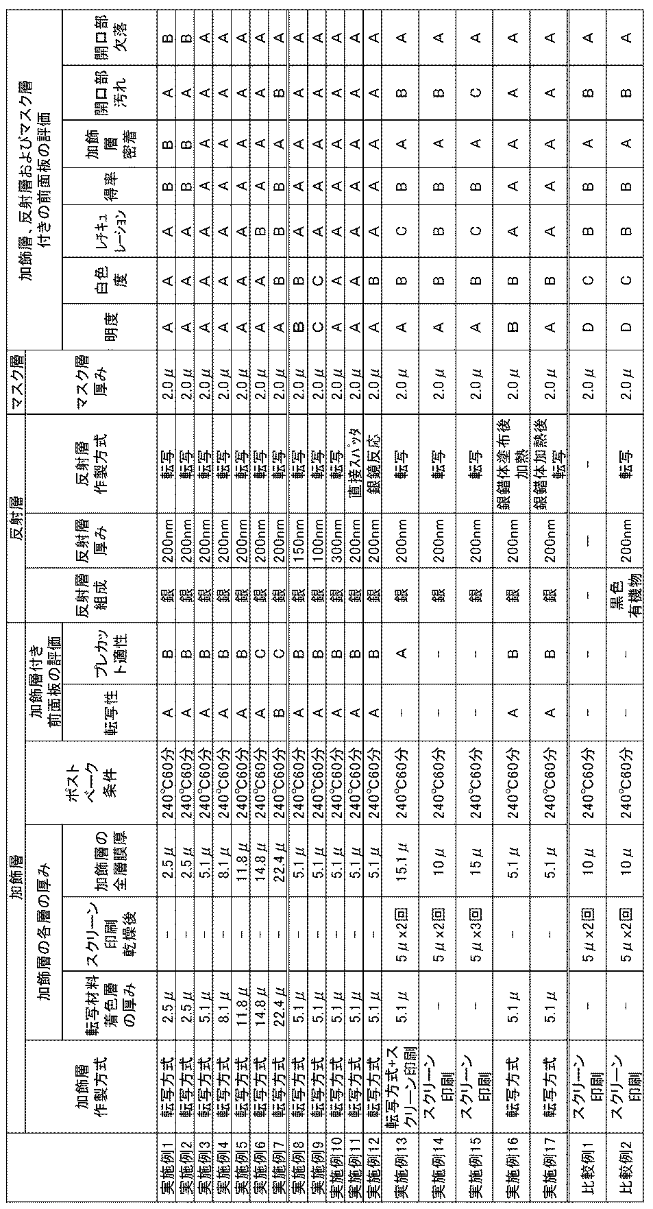
上記表1より、本発明の静電容量型入力装置の製造方法では反射層として金属または無機層の積層体を用いることで、転写後の明度および白色度が良好である白色加飾層を、高い得率で得ることができることがわかった。
また、以上のように、本発明の転写フィルムを用いた本発明の静電容量型入力装置の製造方法によれば、薄層/軽量化のメリットがある静電容量型入力装置を、簡単な工程で高品位に製造可能にすることができた。このため、本発明の製造方法で製造した静電容量型入力装置、およびそれを用いた画像表示装置は高品位であることがわかる。
また、本発明の静電容量型入力装置の製造方法のより好ましい態様によれば、得られた静電容量型入力装置は加飾層のレチキュレーションも良好であり、加飾層密着性も良好であった。さらに、反射層は、第一の透明電極パターン、第二の透明電極パターン、およびこれとは別の導電性要素との間でショートも生じていなかった。
なお、本発明の静電容量型入力装置の製造方法のより好ましい態様によれば、開口部を有する基板を用いた場合でもレジストのはみ出しや、基板裏側の汚染が少ないことがわかった。
また、以上のように、本発明の転写フィルムを用いた本発明の静電容量型入力装置の製造方法によれば、薄層/軽量化のメリットがある静電容量型入力装置を、簡単な工程で高品位に製造可能にすることができた。このため、本発明の製造方法で製造した静電容量型入力装置、およびそれを用いた画像表示装置は高品位であることがわかる。
また、本発明の静電容量型入力装置の製造方法のより好ましい態様によれば、得られた静電容量型入力装置は加飾層のレチキュレーションも良好であり、加飾層密着性も良好であった。さらに、反射層は、第一の透明電極パターン、第二の透明電極パターン、およびこれとは別の導電性要素との間でショートも生じていなかった。
なお、本発明の静電容量型入力装置の製造方法のより好ましい態様によれば、開口部を有する基板を用いた場合でもレジストのはみ出しや、基板裏側の汚染が少ないことがわかった。
1 前面板
1a 前面板の非接触側
2a 加飾層
2b 反射層(無機層の積層体または金属からなる反射層)
2c マスク層
3 第一の透明電極パターン
3a パッド部分
3b 接続部分
4 第二の透明電極パターン
5 絶縁層
6 導電性要素
7 透明保護層
8 開口部
10 静電容量型入力装置
11 強化処理ガラス
12 別の導電性要素
21 仮支持体
22 熱可塑性樹脂層
23 中間層
24 着色層
25 カバーフィルム
31 非画像部
32 画像部
33 刃
C 第1の方向
D 第2の方向
1a 前面板の非接触側
2a 加飾層
2b 反射層(無機層の積層体または金属からなる反射層)
2c マスク層
3 第一の透明電極パターン
3a パッド部分
3b 接続部分
4 第二の透明電極パターン
5 絶縁層
6 導電性要素
7 透明保護層
8 開口部
10 静電容量型入力装置
11 強化処理ガラス
12 別の導電性要素
21 仮支持体
22 熱可塑性樹脂層
23 中間層
24 着色層
25 カバーフィルム
31 非画像部
32 画像部
33 刃
C 第1の方向
D 第2の方向
Claims (20)
- 前面板と、前記前面板の非接触側に少なくとも下記(1)~(3)の要素を有する静電容量型入力装置の製造方法であって、
前記前面板の非接触側に、前記(1)、前記(2)および前記(3)をこの順で積層することを特徴とする静電容量型入力装置の製造方法。
(1)無機白色顔料及びバインダーを含み、膜厚1μm以上30μm未満の加飾層
(2)無機物の積層体または金属からなる反射層
(3)マスク層 - 前記反射層が金属からなることを特徴とする請求項1に記載の静電容量型入力装置の製造方法。
- 前記反射層の厚みが100nm以上であることを特徴とする請求項1または2に記載の静電容量型入力装置の製造方法。
- 少なくとも前記(1)を、着色層を有する転写フィルムを用いて形成することを特徴とする請求項1~3のいずれか一項に記載の静電容量型入力装置の製造方法。
- 前記(1)加飾層を積層した後に、0.08~1.2atmの環境下で110~300℃に加熱する工程を含むことを特徴とする請求項1~4のいずれか1項に記載の静電容量型入力装置の製造方法。
- 前記(3)の要素の上に、透明電極パターンを積層することを特徴とする請求項1~5のいずれか一項に記載の静電容量型入力装置の製造方法。
- 前記(3)の要素の上に、下記(4)~(6)の要素を積層することを特徴とする請求項1~5のいずれか一項に記載の静電容量型入力装置の製造方法。
(4)複数のパッド部分が接続部分を介して第一の方向に延在して形成された複数の第一の透明電極パターン
(5)前記第一の透明電極パターンと電気的に絶縁され、前記第一の方向に交差する方向に延在して形成された複数のパッド部分からなる複数の第二の電極パターン
(6)前記第一の透明電極パターンと前記第二の電極パターンとを電気的に絶縁する絶縁層 - 前記第一の透明電極パターンおよび前記第二の電極パターンの少なくとも一方を、前記前面板の非接触面および前記マスク層の前記前面板とは逆側の面の両方の領域にまたがって設置することを特徴とする請求項7に記載の静電容量型入力装置の製造方法。
- 前記第二の電極パターンが透明電極パターンであることを特徴とする請求項7または8に記載の静電容量型入力装置の製造方法。
- 前記静電容量型入力装置がさらに、(7)前記第一の透明電極パターンおよび前記第二の電極パターンの少なくとも一方に電気的に接続され、前記第一の透明電極パターンおよび前記第二の電極パターンとは別の導電性要素を有することを特徴とする請求項7~9のいずれか一項に記載の静電容量型入力装置の製造方法。
- 前記(7)別の導電性要素を、少なくとも前記マスク層の前面板とは逆側の面側に設置することを特徴とする請求項10に記載の静電容量型入力装置の製造方法。
- 更に、前記(1)~(7)の要素の全てまたは一部を覆うように、(8)透明保護層を設置することを特徴とする請求項10または11に記載の静電容量型入力装置の製造方法。
- 前記透明保護層を、仮支持体と熱可塑性樹脂層と光硬化性樹脂層とをこの順で有する転写フィルムを用いて、前記転写フィルムの光硬化性樹脂層を転写して形成することを特徴とする請求項12に記載の静電容量型入力装置の製造方法。
- 前記第一の透明電極パターン、前記第二の電極パターンおよび前記導電性要素の少なくとも一つを、仮支持体と熱可塑性樹脂層と光硬化性樹脂層とをこの順で有する転写フィルムによって形成されたエッチングパターンを用いて透明導電材料をエッチング処理することによって形成することを特徴とする請求項10~13のいずれか1項に記載の静電容量型入力装置の製造方法。
- 前記第一の透明電極パターン、前記第二の電極パターンおよび前記導電性要素の少なくとも一つを、仮支持体と熱可塑性樹脂層と導電性光硬化性樹脂層とをこの順で有する転写フィルムを用いて、前記転写フィルムの導電性光硬化性樹脂層を転写して形成することを特徴とする請求項10~14のいずれか1項に記載の静電容量型入力装置の製造方法。
- 前記前面板の非接触面に表面処理を行い、
前記表面処理を施した前記前面板の非接触面上に加飾層を設置することを特徴とする請求項1~15のいずれか1項に記載の静電容量型入力装置の製造方法。 - 前記前面板の表面処理に、シラン化合物を用いることを特徴とする請求項16に記載の静電容量型入力装置の製造方法。
- 前記前面板が、少なくとも一部に開口部を有することを特徴とする請求項1~17のいずれか1項に記載の静電容量型入力装置の製造方法。
- 請求項1~18のいずれか1項に記載の静電容量型入力装置の製造方法で製造されたことを特徴とする静電容量型入力装置。
- 請求項19に記載の静電容量型入力装置を構成要素として備えたことを特徴とする画像表示装置。
Priority Applications (1)
| Application Number | Priority Date | Filing Date | Title |
|---|---|---|---|
| CN201380035907.5A CN104508608A (zh) | 2012-09-19 | 2013-08-30 | 静电电容型输入装置的制造方法及静电电容型输入装置、以及具备其的图像显示装置 |
Applications Claiming Priority (2)
| Application Number | Priority Date | Filing Date | Title |
|---|---|---|---|
| JP2012-205459 | 2012-09-19 | ||
| JP2012205459 | 2012-09-19 |
Publications (1)
| Publication Number | Publication Date |
|---|---|
| WO2014045846A1 true WO2014045846A1 (ja) | 2014-03-27 |
Family
ID=50341165
Family Applications (1)
| Application Number | Title | Priority Date | Filing Date |
|---|---|---|---|
| PCT/JP2013/073412 Ceased WO2014045846A1 (ja) | 2012-09-19 | 2013-08-30 | 静電容量型入力装置の製造方法および静電容量型入力装置、並びに、これを備えた画像表示装置 |
Country Status (4)
| Country | Link |
|---|---|
| JP (1) | JP5887314B2 (ja) |
| CN (1) | CN104508608A (ja) |
| TW (1) | TWI595398B (ja) |
| WO (1) | WO2014045846A1 (ja) |
Cited By (3)
| Publication number | Priority date | Publication date | Assignee | Title |
|---|---|---|---|---|
| JP2014093070A (ja) * | 2012-11-05 | 2014-05-19 | Samsung Electro-Mechanics Co Ltd | タッチパネル及びその製造方法 |
| WO2014112429A1 (ja) * | 2013-01-15 | 2014-07-24 | 富士フイルム株式会社 | 耐熱性加飾用着色組成物、静電容量型入力装置の製造方法および静電容量型入力装置、並びに、これを備えた画像表示装置 |
| WO2016060202A1 (ja) * | 2014-10-17 | 2016-04-21 | 旭硝子株式会社 | カバー部材 |
Families Citing this family (4)
| Publication number | Priority date | Publication date | Assignee | Title |
|---|---|---|---|---|
| KR102542864B1 (ko) | 2015-01-19 | 2023-06-14 | 도레이 카부시키가이샤 | 적층 기재, 커버글라스, 터치패널 및 적층 기재의 제조 방법 |
| KR102419615B1 (ko) * | 2015-03-20 | 2022-07-12 | 삼성디스플레이 주식회사 | 표시장치 |
| CN106022261A (zh) * | 2016-05-19 | 2016-10-12 | 信利光电股份有限公司 | 一种盖板在识别传感器的应用、识别模块及盖板 |
| JP2018055175A (ja) | 2016-09-26 | 2018-04-05 | 富士通コンポーネント株式会社 | タッチパネル |
Citations (5)
| Publication number | Priority date | Publication date | Assignee | Title |
|---|---|---|---|---|
| JPS637535A (ja) * | 1986-06-27 | 1988-01-13 | Dainippon Printing Co Ltd | 光カ−ド |
| JP2003075971A (ja) * | 2001-09-04 | 2003-03-12 | Fuji Photo Film Co Ltd | インスタントフイルム |
| JP2009197124A (ja) * | 2008-02-21 | 2009-09-03 | Nitto Denko Corp | 反射及び遮光機能を有する両面粘着テープおよび液晶表示装置 |
| JP2010092739A (ja) * | 2008-10-08 | 2010-04-22 | Sumitomo Electric Printed Circuit Inc | 配線モジュール、その製造方法、および電子機器 |
| JP2012108864A (ja) * | 2010-10-29 | 2012-06-07 | Minebea Co Ltd | 入力装置 |
Family Cites Families (14)
| Publication number | Priority date | Publication date | Assignee | Title |
|---|---|---|---|---|
| JP2008287670A (ja) * | 2007-05-21 | 2008-11-27 | Nissha Printing Co Ltd | 電子機器表示窓のタッチ入力機能付き保護パネル |
| JP5101179B2 (ja) * | 2007-06-13 | 2012-12-19 | 日東電工株式会社 | 装飾用両面粘着シート |
| TW200908839A (en) * | 2007-08-09 | 2009-02-16 | Nichigo Morton Co Ltd | Solder mask, photoresist pattern forming method and the light-emitting device thereof |
| TW201025092A (en) * | 2008-12-30 | 2010-07-01 | Mildex Optical Inc | Touch panel |
| CN201402457Y (zh) * | 2009-03-30 | 2010-02-10 | 深圳欧菲光科技股份有限公司 | 互电容式触摸屏 |
| JP5370944B2 (ja) * | 2010-03-17 | 2013-12-18 | 株式会社ジャパンディスプレイ | タッチパネルおよびその製造方法 |
| TW201213949A (en) * | 2010-09-29 | 2012-04-01 | Catcher Technology Co Ltd | Touch panel |
| JP2012226688A (ja) * | 2011-04-22 | 2012-11-15 | Toppan Printing Co Ltd | 加飾カバーガラス一体型タッチパネルセンサー |
| CN102929454A (zh) * | 2011-08-12 | 2013-02-13 | 宸鸿科技(厦门)有限公司 | 电容式触控面板及降低其金属导体可见度的方法 |
| CN202285071U (zh) * | 2011-10-21 | 2012-06-27 | 比亚迪股份有限公司 | 一种电容触摸屏液晶显示模组 |
| JP6016051B2 (ja) * | 2012-01-25 | 2016-10-26 | 大日本印刷株式会社 | 表示装置用前面保護板、及び表示装置 |
| TWI451374B (zh) * | 2012-02-17 | 2014-09-01 | Innocom Tech Shenzhen Co Ltd | 顯示器螢幕裝置與其製作方法、觸控顯示裝置 |
| CN102662537A (zh) * | 2012-03-07 | 2012-09-12 | 友达光电股份有限公司 | 一种用于增加触控面板的遮蔽层的光密度的方法 |
| JP6415798B2 (ja) * | 2012-04-05 | 2018-10-31 | 大日本印刷株式会社 | 表示装置用前面保護板、及び表示装置 |
-
2013
- 2013-08-28 JP JP2013176636A patent/JP5887314B2/ja active Active
- 2013-08-30 CN CN201380035907.5A patent/CN104508608A/zh active Pending
- 2013-08-30 WO PCT/JP2013/073412 patent/WO2014045846A1/ja not_active Ceased
- 2013-09-06 TW TW102132099A patent/TWI595398B/zh active
Patent Citations (5)
| Publication number | Priority date | Publication date | Assignee | Title |
|---|---|---|---|---|
| JPS637535A (ja) * | 1986-06-27 | 1988-01-13 | Dainippon Printing Co Ltd | 光カ−ド |
| JP2003075971A (ja) * | 2001-09-04 | 2003-03-12 | Fuji Photo Film Co Ltd | インスタントフイルム |
| JP2009197124A (ja) * | 2008-02-21 | 2009-09-03 | Nitto Denko Corp | 反射及び遮光機能を有する両面粘着テープおよび液晶表示装置 |
| JP2010092739A (ja) * | 2008-10-08 | 2010-04-22 | Sumitomo Electric Printed Circuit Inc | 配線モジュール、その製造方法、および電子機器 |
| JP2012108864A (ja) * | 2010-10-29 | 2012-06-07 | Minebea Co Ltd | 入力装置 |
Cited By (3)
| Publication number | Priority date | Publication date | Assignee | Title |
|---|---|---|---|---|
| JP2014093070A (ja) * | 2012-11-05 | 2014-05-19 | Samsung Electro-Mechanics Co Ltd | タッチパネル及びその製造方法 |
| WO2014112429A1 (ja) * | 2013-01-15 | 2014-07-24 | 富士フイルム株式会社 | 耐熱性加飾用着色組成物、静電容量型入力装置の製造方法および静電容量型入力装置、並びに、これを備えた画像表示装置 |
| WO2016060202A1 (ja) * | 2014-10-17 | 2016-04-21 | 旭硝子株式会社 | カバー部材 |
Also Published As
| Publication number | Publication date |
|---|---|
| JP5887314B2 (ja) | 2016-03-16 |
| CN104508608A (zh) | 2015-04-08 |
| JP2014078218A (ja) | 2014-05-01 |
| TW201419109A (zh) | 2014-05-16 |
| TWI595398B (zh) | 2017-08-11 |
Similar Documents
| Publication | Publication Date | Title |
|---|---|---|
| JP5901451B2 (ja) | 透明積層体、静電容量型入力装置および画像表示装置 | |
| JP5914392B2 (ja) | 感光性フィルム、静電容量型入力装置の製造方法および静電容量型入力装置、並びに、これを備えた画像表示装置 | |
| JP5922008B2 (ja) | 転写フィルムおよび透明積層体、それらの製造方法、静電容量型入力装置ならびに画像表示装置 | |
| JP6170288B2 (ja) | 転写材料、静電容量型入力装置の製造方法および静電容量型入力装置、並びに、これを備えた画像表示装置 | |
| JP6336032B2 (ja) | 転写フィルム、転写フィルムの製造方法、透明積層体、透明積層体の製造方法、静電容量型入力装置および画像表示装置 | |
| JP5763492B2 (ja) | 静電容量型入力装置の製造方法および静電容量型入力装置、並びに、これを備えた画像表示装置 | |
| JP5887314B2 (ja) | 静電容量型入力装置の製造方法および静電容量型入力装置、並びに、これを備えた画像表示装置 | |
| JP6030966B2 (ja) | 透明積層体およびその製造方法 | |
| US9632640B2 (en) | Transparent laminate, capacitance type input device, and image display device | |
| CN107003766A (zh) | 转印膜、膜传感器的制造方法、膜传感器、前面板一体型传感器及图像显示装置 | |
| CN108351716A (zh) | 转印薄膜、膜传感器的制造方法、膜传感器、前面板一体型传感器及图像显示装置 | |
| JP6599040B1 (ja) | 転写フィルム、積層体の製造方法、積層体、静電容量型入力装置および画像表示装置 | |
| JP6093891B2 (ja) | 透明積層体、静電容量型入力装置および画像表示装置 | |
| JP6404255B2 (ja) | 転写フィルムおよび透明積層体、それらの製造方法、静電容量型入力装置ならびに画像表示装置 | |
| JP6047298B2 (ja) | 静電容量型入力装置の製造方法および静電容量型入力装置、並びに、これを備えた画像表示装置 | |
| JP6646107B2 (ja) | 転写フィルムおよび透明積層体、それらの製造方法、静電容量型入力装置ならびに画像表示装置 | |
| JP6325019B2 (ja) | 転写材料、静電容量型入力装置の製造方法および静電容量型入力装置、並びに、これを備えた画像表示装置 |
Legal Events
| Date | Code | Title | Description |
|---|---|---|---|
| 121 | Ep: the epo has been informed by wipo that ep was designated in this application |
Ref document number: 13838500 Country of ref document: EP Kind code of ref document: A1 |
|
| NENP | Non-entry into the national phase |
Ref country code: DE |
|
| 122 | Ep: pct application non-entry in european phase |
Ref document number: 13838500 Country of ref document: EP Kind code of ref document: A1 |