WO2014017465A1 - 負荷駆動電源回路 - Google Patents
負荷駆動電源回路 Download PDFInfo
- Publication number
- WO2014017465A1 WO2014017465A1 PCT/JP2013/069869 JP2013069869W WO2014017465A1 WO 2014017465 A1 WO2014017465 A1 WO 2014017465A1 JP 2013069869 W JP2013069869 W JP 2013069869W WO 2014017465 A1 WO2014017465 A1 WO 2014017465A1
- Authority
- WO
- WIPO (PCT)
- Prior art keywords
- switching element
- power supply
- supply circuit
- voltage drop
- forward voltage
- Prior art date
- Legal status (The legal status is an assumption and is not a legal conclusion. Google has not performed a legal analysis and makes no representation as to the accuracy of the status listed.)
- Ceased
Links
Images



Classifications
-
- H—ELECTRICITY
- H02—GENERATION; CONVERSION OR DISTRIBUTION OF ELECTRIC POWER
- H02M—APPARATUS FOR CONVERSION BETWEEN AC AND AC, BETWEEN AC AND DC, OR BETWEEN DC AND DC, AND FOR USE WITH MAINS OR SIMILAR POWER SUPPLY SYSTEMS; CONVERSION OF DC OR AC INPUT POWER INTO SURGE OUTPUT POWER; CONTROL OR REGULATION THEREOF
- H02M3/00—Conversion of DC power input into DC power output
- H02M3/02—Conversion of DC power input into DC power output without intermediate conversion into AC
- H02M3/04—Conversion of DC power input into DC power output without intermediate conversion into AC by static converters
- H02M3/10—Conversion of DC power input into DC power output without intermediate conversion into AC by static converters using discharge tubes with control electrode or semiconductor devices with control electrode
- H02M3/145—Conversion of DC power input into DC power output without intermediate conversion into AC by static converters using discharge tubes with control electrode or semiconductor devices with control electrode using devices of a triode or transistor type requiring continuous application of a control signal
- H02M3/155—Conversion of DC power input into DC power output without intermediate conversion into AC by static converters using discharge tubes with control electrode or semiconductor devices with control electrode using devices of a triode or transistor type requiring continuous application of a control signal using semiconductor devices only
- H02M3/156—Conversion of DC power input into DC power output without intermediate conversion into AC by static converters using discharge tubes with control electrode or semiconductor devices with control electrode using devices of a triode or transistor type requiring continuous application of a control signal using semiconductor devices only with automatic control of output voltage or current, e.g. switching regulators
- H02M3/158—Conversion of DC power input into DC power output without intermediate conversion into AC by static converters using discharge tubes with control electrode or semiconductor devices with control electrode using devices of a triode or transistor type requiring continuous application of a control signal using semiconductor devices only with automatic control of output voltage or current, e.g. switching regulators including plural semiconductor devices as final control devices for a single load
- H02M3/1588—Conversion of DC power input into DC power output without intermediate conversion into AC by static converters using discharge tubes with control electrode or semiconductor devices with control electrode using devices of a triode or transistor type requiring continuous application of a control signal using semiconductor devices only with automatic control of output voltage or current, e.g. switching regulators including plural semiconductor devices as final control devices for a single load comprising at least one synchronous rectifier element
-
- H—ELECTRICITY
- H05—ELECTRIC TECHNIQUES NOT OTHERWISE PROVIDED FOR
- H05B—ELECTRIC HEATING; ELECTRIC LIGHT SOURCES NOT OTHERWISE PROVIDED FOR; CIRCUIT ARRANGEMENTS FOR ELECTRIC LIGHT SOURCES, IN GENERAL
- H05B45/00—Circuit arrangements for operating light-emitting diodes [LED]
- H05B45/30—Driver circuits
- H05B45/37—Converter circuits
- H05B45/3725—Switched mode power supply [SMPS]
-
- Y—GENERAL TAGGING OF NEW TECHNOLOGICAL DEVELOPMENTS; GENERAL TAGGING OF CROSS-SECTIONAL TECHNOLOGIES SPANNING OVER SEVERAL SECTIONS OF THE IPC; TECHNICAL SUBJECTS COVERED BY FORMER USPC CROSS-REFERENCE ART COLLECTIONS [XRACs] AND DIGESTS
- Y02—TECHNOLOGIES OR APPLICATIONS FOR MITIGATION OR ADAPTATION AGAINST CLIMATE CHANGE
- Y02B—CLIMATE CHANGE MITIGATION TECHNOLOGIES RELATED TO BUILDINGS, e.g. HOUSING, HOUSE APPLIANCES OR RELATED END-USER APPLICATIONS
- Y02B70/00—Technologies for an efficient end-user side electric power management and consumption
- Y02B70/10—Technologies improving the efficiency by using switched-mode power supplies [SMPS], i.e. efficient power electronics conversion e.g. power factor correction or reduction of losses in power supplies or efficient standby modes
Definitions
- the present invention relates to a load drive power supply circuit, and more particularly to a load drive power supply circuit that drives a load based on a DC voltage supplied from a DC power supply.
- Patent Document 1 An example of this type of load driving power supply circuit is disclosed in Patent Document 1.
- the FET for synchronous rectification is repeatedly turned on / off during a period when the power supply stop signal is at a low level, that is, during a steady operation period, and the period when the power supply stop signal is at a high level, ie, when the steady operation is stopped. It is continuously turned on during the period.
- the steady operation is stopped, charges are accumulated in the smoothing capacitor. Therefore, if no measures are taken, the load drive power supply circuit is gradually discharged. However, this discharge may adversely affect the operation of the load drive power supply circuit. Therefore, in the prior art document 1, during the stationary operation stop period, the electric charge accumulated in the smoothing capacitor is discharged through the FET in the on state.
- a main object of the present invention is to provide a load driving power supply circuit capable of avoiding an overload of an element due to discharge of electric charges accumulated in a smoothing capacitor.
- a load driving power supply circuit (10: reference numeral corresponding to the embodiment; the same applies hereinafter) includes a first switching element (Q1) having one end connected to one end of a DC power supply (E1), a first switching A second switching element (Q2) having one end connected to the other end of the element and the other end connected to the other end of the DC power supply; an inductor having one end connected to one end of the second switching element ( L1), a smoothing capacitor (C1) provided between the other end of the inductor and the other end of the DC power supply, and a constant current drive for supplying a constant current to a load (18) connected in parallel with the smoothing capacitor.
- First control means for repeatedly turning on and off the first switching element and the second switching element in a complementary manner, and the first switching element to be continuously turned off and the second switching after the constant current drive is completed.
- Elementary Comprising a repeating on / off the second control means (S19 ⁇ S25) an.
- the load includes a diode
- the second control means includes adjustment means (S19) for adjusting the on-duty ratio of the second switching element based on the forward voltage drop of the diode.
- the first detecting means (S3) for detecting the forward voltage drop of the diode is further provided, and the adjusting means refers to the forward voltage drop detected by the first detecting means.
- the second detection means (S35) for detecting the forward drop voltage of the diode is further provided in parallel with the processing of the first control means, and the adjustment means is the forward drop detected by the second detection means. Refer to voltage.
- the adjusting means when it is desired to equalize the time required for discharging the charge accumulated in the smoothing capacitor, the adjusting means increases the on-duty ratio as the forward voltage drop increases, When it is desired to equalize the amount of current flowing through the second switching element, the adjustment means decreases the on-tuty ratio as the forward voltage drop increases.
- Constant current driving is performed by repeatedly turning on and off the first switching element and the second switching element in a complementary manner, and the first switching element is continuously turned off and the second switching element is repeatedly performed after the constant current driving is completed.
- the electric charge accumulated in the smoothing capacitor is gradually discharged through the second switching element.
- load drive power supply circuit 10 of this embodiment corresponds to a synchronous rectification step-down chopper circuit, and includes input terminals T1 and T2 connected to a positive electrode and a negative electrode of DC power supply E1, respectively. Between the input terminals T1 and T2, MOS type field effect transistors (hereinafter simply referred to as “transistors”) Q1 and Q2 connected in series are provided. Specifically, the drain of the transistor Q1 is connected to the input terminal T1, the source of the transistor Q1 is connected to the drain of the transistor Q2, and the source of the transistor Q2 is connected to the input terminal T2.
- transistors MOS type field effect transistors
- An inductor L1 and a smoothing capacitor C1 connected in series with each other are also provided between the drain and source of the transistor Q2.
- the output terminal T3 is connected to the connection point between the inductor L1 and the smoothing capacitor C1, that is, one end of the smoothing capacitor C1
- the output terminal T4 is connected to the connection point between the smoothing capacitor C1 and the source of the transistor Q2, that is, the other end of the smoothing capacitor C1. Is done.
- a light emitting diode 18 and a resistor R1 connected in series are provided between the output terminals T3 and T4.
- the voltage applied to the output terminal T3 corresponds to the forward voltage drop VF of the light emitting diode 18.
- This forward drop voltage VF is detected by a VF detection circuit 16 provided in a DSP (Digital Signal Processor) 12.
- the detected forward drop voltage VF is applied to the switching control circuit 14.
- the terminal voltage of the resistor R1 is input to the switching control circuit 14. Thereby, the switching control circuit 14 can detect the current flowing through the resistor R1, that is, the current flowing through the light emitting diode 18.
- the switching control circuit 14 controls the on / off operation of the transistors Q1 and Q2 with reference to the forward voltage drop VF and the terminal voltage of the resistor R1 thus provided.
- the control procedure follows the flowchart shown in FIGS.
- step S1 switching control circuit 14 starts complementary on / off operations of transistors Q1 and Q2 to preliminarily drive light-emitting diode 18.
- the transistor Q1 is turned on / off at an on-duty ratio such that the light emitting diode 18 is barely lit.
- the transistor Q2 is turned on / off complementarily with respect to the on / off of the transistor Q1 while ensuring a dead time.
- the pulse voltage appearing at the source of the transistor Q1 is smoothed by the inductor L1 and the smoothing capacitor C1.
- a constant current based on a smooth voltage is supplied to the light emitting diode 18, whereby the light emitting diode 18 is lit weakly.
- This step S1 is performed to detect the forward voltage drop VF of the light emitting diode 18 as will be described later.
- step S3 the forward voltage drop VF of the light emitting diode 18 is detected through the VF detection circuit 16.
- the process proceeds to step S5, and the on / off operation of the transistors Q1 and Q2, that is, the preliminary driving of the light emitting diode 18 is stopped. As a result, the light emitting diode 18 is turned off.
- step S7 it is repeatedly determined whether or not a constant current drive start operation has been performed.
- the process proceeds to step S9, and complementary on / off operations of the transistors Q1 and Q2 are started.
- the on-duty ratio of the transistor Q1 gradually increases from zero by the soft start operation, and when the current value detected by the terminal voltage of the resistor R1 reaches the set constant current value, the soft start operation ends.
- the on-duty ratio is adjusted so as to perform a constant current operation.
- the transistor Q2 is turned on / off complementarily with respect to the on / off of the transistor Q1 while ensuring a dead time.
- the pulse voltage appearing at the source of the transistor Q1 is smoothed by the inductor L1 and the smoothing capacitor C1.
- a constant current based on the smoothing voltage is supplied to the light emitting diode 18, thereby turning on the light emitting diode 18.
- step S11 it is determined whether or not a constant current drive stop operation has been performed. If the determination result is NO, the terminal voltage of the resistor R1 is detected in step S13. In step S15, the on-duty ratio of the transistor Q1 is adjusted so that the detected terminal voltage indicates the target voltage, in other words, the current flowing through the light emitting diode 18 is constant. As a result, the light emitting diode 18 is turned on with a desired brightness. When the process of step S15 is completed, the process returns to step S11.
- step S11 When the determination result in step S11 is updated from NO to YES, the on / off operation of the transistors Q1 and Q2 is stopped in step S17. As a result, the constant current driving is terminated and the light emitting diode 18 is turned off.
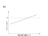
- step S19 the on-duty ratio of the transistor Q2 is adjusted based on the forward voltage drop VF detected in step S3. Referring to FIG. 2, the on-duty ratio of transistor Q2 is increased as the value of forward drop voltage VF increases.
- step S21 the on / off operation of the transistor Q2 is started.
- the transistor Q2 is turned on / off at the on-duty ratio adjusted in step S19, and the electric charge accumulated in the smoothing capacitor C1 is discharged through the inductor L1 and the transistor Q2. Since the on-duty ratio of the transistor Q2 is increased as the forward drop voltage VF increases, the time required for discharging the charge accumulated in the smoothing capacitor C1 can be made uniform.
- step S23 the process waits until the discharge of the smoothing capacitor C1 is completed.
- the on / off operation of the transistor Q2 is stopped in step S25, and then the process ends.
- the drain of the transistor Q1 is connected to the positive electrode of the DC power supply E1
- the source of the transistor Q1 is connected to the drain of the transistor Q2
- the source of the transistor Q2 is connected to the negative electrode of the DC power supply E1.
- One end of the inductor L1 is connected to the drain of the transistor Q2, the other end of the inductor L1 is connected to one end of the smoothing capacitor C1, and the other end of the smoothing capacitor C1 is connected to the negative electrode of the DC power supply E1.
- the switching control circuit 14 repeatedly turns on and off the transistors Q1 and Q2 in a complementary manner for constant current driving for supplying a constant current to the light emitting diode 18 (S9, S13 to S15).
- the switching control circuit 14 also continuously turns off the transistor Q1 and repeatedly turns on / off the transistor Q2 after the end of constant current driving (S19 to S25).
- the larger the forward drop voltage VF the larger the on-duty ratio of the transistor Q2.
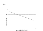
- the larger the forward drop voltage VF the smaller the on-duty ratio of the transistor Q2. Also good.
- the on-duty ratio is adjusted along the graph shown in FIG. By such adjustment, the amount of current flowing through the transistor Q2 during discharge can be made uniform.
- the light emitting diode 18 is preliminarily driven to detect the forward voltage drop VF (see steps S1 to S3 in FIG. 3).
- the forward voltage drop VF may be detected in parallel with the constant current drive of the light emitting diode 18.
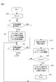
- the flowcharts shown in FIGS. 3 to 4 are partially modified as shown in FIG.
- step S31 is provided instead of the processing of steps S1 to S5. Further, steps S33 to S37 are added following step S15.
- step S31 the flag FLG is set to “0”.
- step S33 it is determined whether or not the flag FLG is “0”. If the determination result is NO, the process returns to step S11 as it is. If the determination result is YES, the process proceeds to steps S11 through S35 to S37. Return.
- step S35 the forward drop voltage VF of the light emitting diode 18 is detected through the VF detection circuit 16. When the detection is completed, the flag FLG is updated to “1” in step S37.
- the forward voltage drop VF is detected in parallel with the constant current drive of the light emitting diode 18, but the forward voltage drop VF responds to the constant current drive stop operation. May be detected.
- the processes of steps S1 to S5 shown in FIG. 3 are omitted, and a process corresponding to the process of step S3 is executed between steps S17 and S19.
Landscapes
- Engineering & Computer Science (AREA)
- Power Engineering (AREA)
- Dc-Dc Converters (AREA)
- Led Devices (AREA)
Description
この発明は、負荷駆動電源回路に関し、特に直流電源から供給された直流電圧に基づいて負荷を駆動する、負荷駆動電源回路に関する。
この種の負荷駆動電源回路の一例が、特許文献1に開示されている。この背景技術によれば、同期整流用のFETは、電力供給停止信号がローレベルの期間、つまり定常動作期間に繰り返しオン/オフされ、電力供給停止信号がハイレベルの期間、つまり定常動作の停止期間に継続的にオンされる。定常動作が停止したとき、平滑コンデンサには電荷が蓄積されている。したがって、何の対策も講じなければ負荷駆動電源回路内で徐々に放電されることになる。しかし、この放電により負荷駆動電源回路の動作に悪影響を与える場合もある。したがって先行文献1では、定常動作の停止期間において、平滑コンデンサに蓄積された電荷は、オン状態のFETを介して放電される。
放電のために同期整流用のFETをオンすると、平滑コンデンサに蓄積された電荷に基づく電流がFETを導通する。しかし、平滑コンデンサに蓄積された電荷が大きい場合には、大電流がFETを瞬間的に導通するため、FETやインダクタの定格電流値を超える電流が流れるおそれがある。
それゆえに、この発明の主たる目的は、平滑コンデンサに蓄積された電荷の放電に起因する素子の過負荷を回避することができる、負荷駆動電源回路を提供することである。
この発明に従う負荷駆動電源回路(10:実施例で相当する参照符号。以下同じ)は、直流電源(E1)の一方端に接続された一方端を有する第1スイッチング素子(Q1)、第1スイッチング素子の他方端に接続された一方端と直流電源の他方端に接続された他方端とを有する第2スイッチング素子(Q2)、第2スイッチング素子の一方端に接続された一方端を有するインダクタ(L1)、インダクタの他方端および直流電源の他方端の間に設けられた平滑コンデンサ(C1)、平滑コンデンサと並列に接続される負荷(18)に定電流を供給する定電流駆動のために第1スイッチング素子および第2スイッチング素子を相補的に繰り返しオン/オフする第1制御手段(S9, S13~S15)、ならびに定電流駆動の終了後に第1スイッチング素子を継続的にオフしかつ第2スイッチング素子を繰り返しオン/オフする第2制御手段(S19~S25)を備える。
好ましくは、負荷はダイオードを含み、第2制御手段はダイオードの順方向降下電圧に基づいて第2スイッチング素子のオンデューティ比を調整する調整手段(S19)を含む。
或る局面では、第1制御手段の処理に先立って第1スイッチング素子および第2スイッチング素子を相補的に繰り返しオン/オフする予備駆動を実行する第3制御手段(S1)、および予備駆動と並列してダイオードの順方向降下電圧を検出する第1検出手段(S3)がさらに備えられ、調整手段は第1検出手段によって検出された順方向降下電圧を参照する。
他の局面では、第1制御手段の処理と並列してダイオードの順方向降下電圧を検出する第2検出手段(S35)がさらに備えられ、調整手段は第2検出手段によって検出された順方向降下電圧を参照する。
この発明において、平滑コンデンサに蓄積された電荷の放電に要する時間の均一化を図ることが望まれる場合には、調整手段は順方向降下電圧が大きいほどオンデューティ比を大きくし、他方、放電時に第2スイッチング素子を流れる電流量の均一化を図ることが望まれる場合には、調整手段は順方向降下電圧が大きいほどオンテューティ比を小さくする。
第1スイッチング素子および第2スイッチング素子を相補的に繰り返しオン/オフすることで定電流駆動が行われ、定電流駆動の終了後に第1スイッチング素子が継続的にオフされかつ第2スイッチング素子が繰り返しオン/オフされることで、平滑コンデンサに蓄積された電荷が第2スイッチング素子を介して徐々に放電される。これによって、平滑コンデンサに蓄積された電荷の放電に起因する素子の過負荷を回避することができる。
この発明の上述の目的,その他の目的,特徴および利点は、図面を参照して行う以下の実施例の詳細な説明から一層明らかとなろう。
図1を参照して、この実施例の負荷駆動電源回路10は、同期整流式の降圧チョッパ回路に相当し、直流電源E1の正極および負極とそれぞれ接続される入力端子T1およびT2を含む。入力端子T1およびT2の間には、互いに直列接続されたMOS型の電界効果トランジスタ(以下、単に「トランジスタ」という。)Q1およびQ2が設けられる。詳しくは、トランジスタQ1のドレインが入力端子T1と接続され、トランジスタQ1のソースがトランジスタQ2のドレインと接続され、そしてトランジスタQ2のソースが入力端子T2と接続される。
トランジスタQ2のドレインとソースとの間にはまた、互いに直列接続されたインダクタL1および平滑コンデンサC1が設けられる。出力端子T3はインダクタL1と平滑コンデンサC1との接続点つまり平滑コンデンサC1の一方端に接続され、出力端子T4は平滑コンデンサC1とトランジスタQ2のソースとの接続点つまり平滑コンデンサC1の他方端に接続される。
出力端子T3およびT4の間には、互いに直列接続された発光ダイオード18および抵抗R1が設けられる。出力端子T3に印加された電圧は、発光ダイオード18の順方向降下電圧VFに相当する。この順方向降下電圧VFは、DSP(Digital Signal Processor)12に設けられたVF検出回路16によって検出される。検出された順方向降下電圧VFは、スイッチング制御回路14に与えられる。また、スイッチング制御回路14には、抵抗R1の端子電圧が入力される。これにより、スイッチング制御回路14は、抵抗R1に流れる電流、つまり発光ダイオード18に流れる電流を検出できる。
スイッチング制御回路14は、こうして与えられた順方向降下電圧VFおよび抵抗R1の端子電圧を参照して、トランジスタQ1およびQ2のオン/オフ動作を制御する。制御の手順は、図3~図4に示すフロー図に従う。
図3を参照して、スイッチング制御回路14は、ステップS1では、発光ダイオード18を予備的に駆動するべく、トランジスタQ1およびQ2の相補的なオン/オフ動作を開始する。トランジスタQ1は、発光ダイオード18が辛うじて点灯する程度のオンデューティ比でオン/オフされる。トランジスタQ2は、デッドタイムを確保しつつ、トランジスタQ1のオン/オフに対して相補的にオン/オフされる。トランジスタQ1のソースに現れたパルス電圧は、インダクタL1と平滑コンデンサC1とによって平滑される。発光ダイオード18には平滑電圧に基づく定電流が供給され、これによって発光ダイオード18が弱く点灯する。このステップS1は、後述するように発光ダイオード18の順方向降下電圧VFを検出するために行われる。
ステップS3では、VF検出回路16を通して発光ダイオード18の順方向降下電圧VFを検出する。検出が完了するとステップS5に進み、トランジスタQ1およびQ2のオン/オフ動作つまり発光ダイオード18の予備駆動を停止する。これによって、発光ダイオード18が消灯する。
ステップS7では、定電流駆動開始操作が行われたか否かを繰り返し判別する。発光ダイオード18の定電流駆動開始をオンするタイミングにおいて判別結果がNOからYESに更新されるとステップS9に進み、トランジスタQ1およびQ2の相補的なオン/オフ動作を開始する。このとき、トランジスタQ1のオンデューティ比はソフトスタート動作により、ゼロから徐々に大きくなり、抵抗R1の端子電圧により検出された電流値が設定された定電流値に達するとソフトスタート動作は終了し、次には定電流動作を行うようにオンデューティ比が調整される。トランジスタQ2は、デッドタイムを確保しつつ、トランジスタQ1のオン/オフに対して相補的にオン/オフされる。
上述と同様、トランジスタQ1のソースに現れたパルス電圧は、インダクタL1と平滑コンデンサC1とによって平滑される。発光ダイオード18には平滑電圧に基づく定電流が供給され、これによって発光ダイオード18が点灯する。
ステップS11では定電流駆動停止操作が行われたか否かを判別し、判別結果がNOであればステップS13で抵抗R1の端子電圧を検出する。ステップS15では、検出された端子電圧が目標電圧を示すように、換言すれば発光ダイオード18に流れる電流が一定になるようにトランジスタQ1のオンデューティ比を調整する。この結果、発光ダイオード18が所望の明るさで点灯する。ステップS15の処理が完了すると、ステップS11に戻る。
ステップS11の判別結果がNOからYESに更新されると、ステップS17でトランジスタQ1およびQ2のオン/オフ動作を停止する。これによって、定電流駆動が終了され、発光ダイオード18が消灯する。ステップS19では、ステップS3で検出された順方向降下電圧VFに基づいてトランジスタQ2のオンデューティ比を調整する。図2を参照して、トランジスタQ2のオンデューティ比は順方向降下電圧VFの値が増大するほど大きくされる。
ステップS21では、トランジスタQ2のオン/オフ動作を開始する。トランジスタQ2はステップS19で調整されたオンデューティ比でオン/オフされ、平滑コンデンサC1に蓄積された電荷はインダクタL1およびトランジスタQ2を通して放電される。トランジスタQ2のオンデューティ比は順方向降下電圧VFの増大に応じて増大されるため、平滑コンデンサC1に蓄積された電荷の放電に要する時間の均一化が図られる。
ステップS23では、平滑コンデンサC1の放電が完了するまで待機する。平滑コンデンサC1の放電が完了すると、ステップS25でトランジスタQ2のオン/オフ動作を停止し、その後に処理を終了する。
以上の説明から分かるように、トランジスタQ1のドレインは直流電源E1の正極に接続され、トランジスタQ1のソースはトランジスタQ2のドレインに接続され、そしてトランジスタQ2のソースは直流電源E1の負極に接続される。インダクタL1の一方端はトランジスタQ2のドレインに接続され、インダクタL1の他方端は平滑コンデンサC1の一方端に接続され、そして平滑コンデンサC1の他方端は直流電源E1の負極に接続される。スイッチング制御回路14は、発光ダイオード18に定電流を供給する定電流駆動のために、トランジスタQ1およびQ2を相補的に繰り返しオン/オフする(S9, S13~S15)。スイッチング制御回路14はまた、定電流駆動の終了後に、トランジスタQ1を継続的にオフしかつトランジスタQ2を繰り返しオン/オフする(S19~S25)。
トランジスタQ1およびQ2を相補的に繰り返しオン/オフすることで定電流駆動が実現されるところ、定電流駆動の終了後にトランジスタQ1を継続的にオフしかつトランジスタQ2を繰り返しオン/オフすることで、平滑コンデンサC1に蓄積された電荷がトランジスタQ2を介して徐々に放電される。これによって、平滑コンデンサC1に蓄積された電荷の放電に起因するインダクタL1およびトランジスタQ2の過負荷を回避することができる。
なお、この実施例では、順方向降下電圧VFが大きいほどトランジスタQ2のオンデューティ比を大きくするようにしているが、順方向降下電圧VFが大きいほどトランジスタQ2のオンデューティ比を小さくするようにしてもよい。この場合、オンデューティ比は、図5に示すグラフに沿って調整される。このような調整によって、放電時にトランジスタQ2を流れる電流量の均一化が図られる。
また、この実施例では、順方向降下電圧VFを検出するために発光ダイオード18を予備的に駆動するようにしている(図3のステップS1~S3参照)。しかし、順方向降下電圧VFは発光ダイオード18の定電流駆動と並列して検出されるようにしてもよい。この場合、図3~図4に示すフロー図は、図6に示すように部分的に修正される。
図6によれば、ステップS1~S5の処理に代えてステップS31が設けられる。また、ステップS15に続いてステップS33~S37の処理が追加される。ステップS31では、フラグFLGを“0”に設定する。ステップS33ではフラグFLGが“0”であるか否かを判別し、判別結果がNOであればそのままステップS11に戻る一方、判別結果がYESであればステップS35~S37の処理を経てステップS11に戻る。ステップS35では、VF検出回路16を通して発光ダイオード18の順方向降下電圧VFを検出する。検出が完了すると、ステップS37でフラグFLGを“1”に更新する。
図6を参照して説明した実施例では、順方向降下電圧VFは発光ダイオード18の定電流駆動と並列して検出するようにしたが、順方向降下電圧VFは、定電流駆動停止操作に応答して検出されるようにしてもよい。この場合、図3に示すステップS1~S5の処理が省略され、ステップS3の処理に相当する処理がステップS17およびS19の間に実行される。
10 …負荷駆動電源回路
12 …DSP
14 …SW制御回路
16 …VF検出回路
18 …ダイオード負荷
Q1,Q2 …トランジスタ
C1 …平滑コンデンサ
L1 …インダクタ
R1 …抵抗
12 …DSP
14 …SW制御回路
16 …VF検出回路
18 …ダイオード負荷
Q1,Q2 …トランジスタ
C1 …平滑コンデンサ
L1 …インダクタ
R1 …抵抗
Claims (6)
- 直流電源の一方端に接続された一方端を有する第1スイッチング素子、
前記第1スイッチング素子の他方端に接続された一方端と前記直流電源の他方端に接続された他方端とを有する第2スイッチング素子、
前記第2スイッチング素子の一方端に接続された一方端を有するインダクタ、
前記インダクタの他方端および前記直流電源の他方端の間に設けられた平滑コンデンサ、
前記平滑コンデンサと並列に接続される負荷に定電流を供給する定電流駆動のために前記第1スイッチング素子および前記第2スイッチング素子を相補的に繰り返しオン/オフする第1制御手段、ならびに
前記定電流駆動の終了後に前記第1スイッチング素子を継続的にオフしかつ前記第2スイッチング素子を繰り返しオン/オフする第2制御手段を備える、負荷駆動電源回路。 - 前記負荷はダイオードを含み、
前記第2制御手段は前記ダイオードの順方向降下電圧に基づいて前記第2スイッチング素子のオンデューティ比を調整する調整手段を含む、請求項1記載の負荷駆動電源回路。 - 前記第1制御手段の処理に先立って前記第1スイッチング素子および前記第2スイッチング素子を相補的に繰り返しオン/オフする予備駆動を実行する第3制御手段、および
前記予備駆動と並列して前記ダイオードの順方向降下電圧を検出する第1検出手段をさらに備え、
前記調整手段は前記第1検出手段によって検出された順方向降下電圧を参照する、請求項2記載の負荷駆動電源回路。 - 前記第1制御手段の処理と並列して前記ダイオードの順方向降下電圧を検出する第2検出手段をさらに備え、
前記調整手段は前記第2検出手段によって検出された順方向降下電圧を参照する、請求項2記載の負荷駆動電源回路。 - 前記調整手段は前記順方向降下電圧が大きいほどオンデューティ比を大きくする、請求項2ないし4のいずれかに記載の負荷駆動電源回路。
- 前記調整手段は前記順方向降下電圧が大きいほどオンテューティ比を小さくする、請求項2ないし4のいずれかに記載の負荷駆動電源回路。
Applications Claiming Priority (2)
| Application Number | Priority Date | Filing Date | Title |
|---|---|---|---|
| JP2012-166190 | 2012-07-26 | ||
| JP2012166190A JP2015180115A (ja) | 2012-07-26 | 2012-07-26 | 負荷駆動電源回路 |
Publications (1)
| Publication Number | Publication Date |
|---|---|
| WO2014017465A1 true WO2014017465A1 (ja) | 2014-01-30 |
Family
ID=49997275
Family Applications (1)
| Application Number | Title | Priority Date | Filing Date |
|---|---|---|---|
| PCT/JP2013/069869 Ceased WO2014017465A1 (ja) | 2012-07-26 | 2013-07-23 | 負荷駆動電源回路 |
Country Status (2)
| Country | Link |
|---|---|
| JP (1) | JP2015180115A (ja) |
| WO (1) | WO2014017465A1 (ja) |
Cited By (3)
| Publication number | Priority date | Publication date | Assignee | Title |
|---|---|---|---|---|
| WO2016052065A1 (ja) * | 2014-10-02 | 2016-04-07 | ローム株式会社 | 発光素子駆動装置、発光装置、車両 |
| JP2017011906A (ja) * | 2015-06-23 | 2017-01-12 | トレックス・セミコンダクター株式会社 | スイッチング電源回路 |
| JP2021048174A (ja) * | 2019-09-17 | 2021-03-25 | パナソニックIpマネジメント株式会社 | 半導体光源駆動装置及び投写型映像表示装置 |
Families Citing this family (1)
| Publication number | Priority date | Publication date | Assignee | Title |
|---|---|---|---|---|
| JP6715068B2 (ja) * | 2016-04-25 | 2020-07-01 | 株式会社アイ・ライティング・システム | スイッチング変換方式のled電源回路 |
Citations (4)
| Publication number | Priority date | Publication date | Assignee | Title |
|---|---|---|---|---|
| JP2809827B2 (ja) * | 1990-07-03 | 1998-10-15 | 東芝エンジニアリング株式会社 | チョッパ制御方法 |
| JP2006033990A (ja) * | 2004-07-15 | 2006-02-02 | Toshiba Microelectronics Corp | Dc/dcコンバータ及び半導体集積回路 |
| JP2007089371A (ja) * | 2005-09-26 | 2007-04-05 | Pioneer Electronic Corp | バックコンバータ |
| JP2009296713A (ja) * | 2008-06-03 | 2009-12-17 | Mitsumi Electric Co Ltd | Dc−dcコンバータおよび電源制御用半導体集積回路 |
-
2012
- 2012-07-26 JP JP2012166190A patent/JP2015180115A/ja active Pending
-
2013
- 2013-07-23 WO PCT/JP2013/069869 patent/WO2014017465A1/ja not_active Ceased
Patent Citations (4)
| Publication number | Priority date | Publication date | Assignee | Title |
|---|---|---|---|---|
| JP2809827B2 (ja) * | 1990-07-03 | 1998-10-15 | 東芝エンジニアリング株式会社 | チョッパ制御方法 |
| JP2006033990A (ja) * | 2004-07-15 | 2006-02-02 | Toshiba Microelectronics Corp | Dc/dcコンバータ及び半導体集積回路 |
| JP2007089371A (ja) * | 2005-09-26 | 2007-04-05 | Pioneer Electronic Corp | バックコンバータ |
| JP2009296713A (ja) * | 2008-06-03 | 2009-12-17 | Mitsumi Electric Co Ltd | Dc−dcコンバータおよび電源制御用半導体集積回路 |
Cited By (9)
| Publication number | Priority date | Publication date | Assignee | Title |
|---|---|---|---|---|
| WO2016052065A1 (ja) * | 2014-10-02 | 2016-04-07 | ローム株式会社 | 発光素子駆動装置、発光装置、車両 |
| JP2016074255A (ja) * | 2014-10-02 | 2016-05-12 | ローム株式会社 | 発光素子駆動装置、発光装置、車両 |
| CN106794793A (zh) * | 2014-10-02 | 2017-05-31 | 罗姆股份有限公司 | 发光元件驱动装置、发光装置和车辆 |
| US9986611B2 (en) | 2014-10-02 | 2018-05-29 | Rohm Co., Ltd. | Light-emitting element driving device, light-emitting device, and vehicle |
| CN106794793B (zh) * | 2014-10-02 | 2019-08-06 | 罗姆股份有限公司 | 发光元件驱动装置、发光装置和车辆 |
| US10390402B2 (en) | 2014-10-02 | 2019-08-20 | Rohm Co., Ltd. | Light-emitting element driving device, light-emitting device, and vehicle |
| JP2017011906A (ja) * | 2015-06-23 | 2017-01-12 | トレックス・セミコンダクター株式会社 | スイッチング電源回路 |
| JP2021048174A (ja) * | 2019-09-17 | 2021-03-25 | パナソニックIpマネジメント株式会社 | 半導体光源駆動装置及び投写型映像表示装置 |
| JP7386437B2 (ja) | 2019-09-17 | 2023-11-27 | パナソニックIpマネジメント株式会社 | 半導体光源駆動装置及び投写型映像表示装置 |
Also Published As
| Publication number | Publication date |
|---|---|
| JP2015180115A (ja) | 2015-10-08 |
Similar Documents
| Publication | Publication Date | Title |
|---|---|---|
| US20120274235A1 (en) | Power Converting Circuit and Converting Controller | |
| US20150188425A1 (en) | Buck converter and control method therefor | |
| US8994286B2 (en) | Operating device for a lamp having a power correction circuit | |
| US9769889B2 (en) | Driving circuit for flash light-emitting diode and operating method thereof | |
| WO2014017465A1 (ja) | 負荷駆動電源回路 | |
| JP2013503556A5 (ja) | ||
| WO2011031395A3 (en) | Power transistor with turn off control and method for operating | |
| TWI509968B (zh) | 電壓轉換電路以及電壓轉換控制器與應用於其中的參數設定方法 | |
| CN103915889A (zh) | 切换电源转换装置及其切换控制器与驱动方法 | |
| JP2011061891A5 (ja) | ||
| WO2014043977A1 (zh) | 一种电源系统及其启动方法 | |
| JP2005176476A (ja) | スイッチングレギュレータ | |
| JP2017011790A (ja) | スイッチング素子の駆動装置 | |
| TW201501455A (zh) | 直流升壓轉換器 | |
| TWM453302U (zh) | 切換式電源供應器及其控制電路 | |
| JP6668684B2 (ja) | 点灯装置および照明器具 | |
| US7982408B2 (en) | Cold-cathode fluorescent lamp (CCFL) current control circuit | |
| CN107404217B (zh) | 开关电源控制电路和方法及开关电源 | |
| CN109039075A (zh) | 一种开关电路的控制方法、控制电路及开关电路 | |
| JP6307923B2 (ja) | 点灯装置および照明器具 | |
| JP2023106340A5 (ja) | ||
| CN209120064U (zh) | 一种开关电路的控制电路及开关电路 | |
| CN102281686A (zh) | Led灯在输入电压快速跌落时的补偿控制装置及其方法 | |
| JP6587054B2 (ja) | 点灯装置及び照明器具 | |
| JP2004129419A (ja) | 突入電流防止回路の動作方法および突入電流防止回路 |
Legal Events
| Date | Code | Title | Description |
|---|---|---|---|
| 121 | Ep: the epo has been informed by wipo that ep was designated in this application |
Ref document number: 13822461 Country of ref document: EP Kind code of ref document: A1 |
|
| NENP | Non-entry into the national phase |
Ref country code: DE |
|
| 122 | Ep: pct application non-entry in european phase |
Ref document number: 13822461 Country of ref document: EP Kind code of ref document: A1 |
|
| NENP | Non-entry into the national phase |
Ref country code: JP |