WO2014017253A1 - 電源装置 - Google Patents
電源装置 Download PDFInfo
- Publication number
- WO2014017253A1 WO2014017253A1 PCT/JP2013/067764 JP2013067764W WO2014017253A1 WO 2014017253 A1 WO2014017253 A1 WO 2014017253A1 JP 2013067764 W JP2013067764 W JP 2013067764W WO 2014017253 A1 WO2014017253 A1 WO 2014017253A1
- Authority
- WO
- WIPO (PCT)
- Prior art keywords
- power supply
- supply device
- power
- switching element
- circuit
- Prior art date
- Legal status (The legal status is an assumption and is not a legal conclusion. Google has not performed a legal analysis and makes no representation as to the accuracy of the status listed.)
- Ceased
Links
Images


Classifications
-
- H—ELECTRICITY
- H02—GENERATION; CONVERSION OR DISTRIBUTION OF ELECTRIC POWER
- H02M—APPARATUS FOR CONVERSION BETWEEN AC AND AC, BETWEEN AC AND DC, OR BETWEEN DC AND DC, AND FOR USE WITH MAINS OR SIMILAR POWER SUPPLY SYSTEMS; CONVERSION OF DC OR AC INPUT POWER INTO SURGE OUTPUT POWER; CONTROL OR REGULATION THEREOF
- H02M3/00—Conversion of DC power input into DC power output
- H02M3/22—Conversion of DC power input into DC power output with intermediate conversion into AC
- H02M3/24—Conversion of DC power input into DC power output with intermediate conversion into AC by static converters
- H02M3/28—Conversion of DC power input into DC power output with intermediate conversion into AC by static converters using discharge tubes with control electrode or semiconductor devices with control electrode to produce the intermediate AC
- H02M3/325—Conversion of DC power input into DC power output with intermediate conversion into AC by static converters using discharge tubes with control electrode or semiconductor devices with control electrode to produce the intermediate AC using devices of a triode or a transistor type requiring continuous application of a control signal
- H02M3/335—Conversion of DC power input into DC power output with intermediate conversion into AC by static converters using discharge tubes with control electrode or semiconductor devices with control electrode to produce the intermediate AC using devices of a triode or a transistor type requiring continuous application of a control signal using semiconductor devices only
- H02M3/33569—Conversion of DC power input into DC power output with intermediate conversion into AC by static converters using discharge tubes with control electrode or semiconductor devices with control electrode to produce the intermediate AC using devices of a triode or a transistor type requiring continuous application of a control signal using semiconductor devices only having several active switching elements
- H02M3/33576—Conversion of DC power input into DC power output with intermediate conversion into AC by static converters using discharge tubes with control electrode or semiconductor devices with control electrode to produce the intermediate AC using devices of a triode or a transistor type requiring continuous application of a control signal using semiconductor devices only having several active switching elements having at least one active switching element at the secondary side of an isolation transformer
- H02M3/33592—Conversion of DC power input into DC power output with intermediate conversion into AC by static converters using discharge tubes with control electrode or semiconductor devices with control electrode to produce the intermediate AC using devices of a triode or a transistor type requiring continuous application of a control signal using semiconductor devices only having several active switching elements having at least one active switching element at the secondary side of an isolation transformer having a synchronous rectifier circuit or a synchronous freewheeling circuit at the secondary side of an isolation transformer
-
- H—ELECTRICITY
- H02—GENERATION; CONVERSION OR DISTRIBUTION OF ELECTRIC POWER
- H02M—APPARATUS FOR CONVERSION BETWEEN AC AND AC, BETWEEN AC AND DC, OR BETWEEN DC AND DC, AND FOR USE WITH MAINS OR SIMILAR POWER SUPPLY SYSTEMS; CONVERSION OF DC OR AC INPUT POWER INTO SURGE OUTPUT POWER; CONTROL OR REGULATION THEREOF
- H02M3/00—Conversion of DC power input into DC power output
- H02M3/22—Conversion of DC power input into DC power output with intermediate conversion into AC
- H02M3/24—Conversion of DC power input into DC power output with intermediate conversion into AC by static converters
- H02M3/28—Conversion of DC power input into DC power output with intermediate conversion into AC by static converters using discharge tubes with control electrode or semiconductor devices with control electrode to produce the intermediate AC
- H02M3/325—Conversion of DC power input into DC power output with intermediate conversion into AC by static converters using discharge tubes with control electrode or semiconductor devices with control electrode to produce the intermediate AC using devices of a triode or a transistor type requiring continuous application of a control signal
- H02M3/335—Conversion of DC power input into DC power output with intermediate conversion into AC by static converters using discharge tubes with control electrode or semiconductor devices with control electrode to produce the intermediate AC using devices of a triode or a transistor type requiring continuous application of a control signal using semiconductor devices only
- H02M3/337—Conversion of DC power input into DC power output with intermediate conversion into AC by static converters using discharge tubes with control electrode or semiconductor devices with control electrode to produce the intermediate AC using devices of a triode or a transistor type requiring continuous application of a control signal using semiconductor devices only in push-pull configuration
- H02M3/3376—Conversion of DC power input into DC power output with intermediate conversion into AC by static converters using discharge tubes with control electrode or semiconductor devices with control electrode to produce the intermediate AC using devices of a triode or a transistor type requiring continuous application of a control signal using semiconductor devices only in push-pull configuration with automatic control of output voltage or current
-
- Y—GENERAL TAGGING OF NEW TECHNOLOGICAL DEVELOPMENTS; GENERAL TAGGING OF CROSS-SECTIONAL TECHNOLOGIES SPANNING OVER SEVERAL SECTIONS OF THE IPC; TECHNICAL SUBJECTS COVERED BY FORMER USPC CROSS-REFERENCE ART COLLECTIONS [XRACs] AND DIGESTS
- Y02—TECHNOLOGIES OR APPLICATIONS FOR MITIGATION OR ADAPTATION AGAINST CLIMATE CHANGE
- Y02B—CLIMATE CHANGE MITIGATION TECHNOLOGIES RELATED TO BUILDINGS, e.g. HOUSING, HOUSE APPLIANCES OR RELATED END-USER APPLICATIONS
- Y02B70/00—Technologies for an efficient end-user side electric power management and consumption
- Y02B70/10—Technologies improving the efficiency by using switched-mode power supplies [SMPS], i.e. efficient power electronics conversion e.g. power factor correction or reduction of losses in power supplies or efficient standby modes
Definitions
- the present invention relates to a power supply apparatus that converts input DC power into DC power having a predetermined voltage.
- a power supply device converts input DC power into DC power having a predetermined voltage and supplies the DC power to the outside.
- the power supply apparatus is connected to a transformer circuit and a primary side of the transformer circuit, and is input to the DC power. Is converted into AC power and output to a transformer circuit, and a rectifier circuit connected to the secondary side of the transformer circuit and converting AC power transformed by the transformer circuit into DC power.
- the rectifier circuit is electrically connected in parallel with each other to a plurality of first switching elements electrically connected in parallel to one end on the secondary side of the transformer circuit and to the other end on the secondary side of the transformer circuit.
- a plurality of second switching elements, and a plurality of capacitor elements electrically connected in parallel to each of the first switching element and the second switching element.
- a high-efficiency and low-noise power supply device can be provided.
- FIG. 1 is a block diagram showing a configuration of a power supply system including a power supply device according to an embodiment of the present invention.
- This power supply system is used by being mounted on a vehicle driven by an electric motor such as an electric vehicle or a hybrid vehicle.
- the power supply system shown in FIG. 1 includes a power supply device 1, an auxiliary battery 9, an electrical component 10, and a high voltage battery 11.
- the power supply device 1 and the high voltage battery 11 are covered with conductive metal cases 111 and 121, respectively, and are connected to each other via shield wires 12a and 12b.
- the case 111 of the power supply device 1 is fixed to the vehicle chassis 8 by metal bolts 13a and 13b.
- the case 121 of the high voltage battery 11 is fixed to the chassis 8 by metal bolts 13c and 13d. Thereby, the power supply device 1 and the high voltage battery 11 are electrically connected to the chassis 8 and grounded to a common vehicle ground.
- the power supply device 1 includes a DC / AC converter circuit 2, a transformer 3, a rectifier circuit 4, and a control circuit 5. These are housed in the case 111 and are grounded with the potential of the case 111 as a common ground (GND) potential.
- a metal bolt 13 e connected to one end of the grounding cable 7 is attached to the case 111.
- the other end of the grounding cable 7 is connected to a metal bolt 13 f attached to the chassis 8.
- the case 111 and the chassis 8 are electrically connected via the grounding cable 7 so that the portion of the chassis 8 to which the bolts 13f are attached in addition to the grounding by the bolts 13a and 13b described above.
- the power supply device 1 is further grounded.
- the power supply device 1 includes a DC / AC conversion circuit 2 that converts high-voltage DC power input from the high-voltage battery 11 through the shielded wires 12a and 12b into AC power, and AC power output from the DC / AC conversion circuit 2.
- a rectifier circuit 3 for converting AC power transformed by the transformer 3 into low-voltage DC power
- the control circuit 5 performs on / off control of switching elements respectively provided in the DC / AC conversion circuit 2 and the rectifier circuit 4 to operate these circuits in synchronism and perform the power conversion as described above. .
- the power supply device 1 converts the high-voltage DC power output from the high-voltage battery 11 into low-voltage DC power, and outputs the DC power after the voltage conversion to the auxiliary battery 9 and the electrical component 10. can do.
- the (+) side output of the rectifier circuit 4 is connected to the auxiliary battery 9 and the (+) terminal of the electrical component 10 via the output terminal 6 provided in the case 111.
- the ( ⁇ ) side output of the rectifier circuit 4 is connected to the ( ⁇ ) terminal of the auxiliary battery 9 via the bolt 13e, the grounding cable 7 and the bolt 13f. Further, it is connected to the ( ⁇ ) terminal of the electrical component 10 through the bolt 13e, the grounding cable 7, the bolt 13f, and the chassis 8. Thereby, DC power is supplied from the high voltage battery 11 to the auxiliary battery 9 and the electrical component 10 via the power supply device 1.
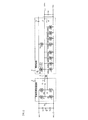
- FIG. 2 is a circuit diagram showing an example of the circuit configuration of the DC / AC converter circuit 2, the transformer 3 and the rectifier circuit 4.
- the DC / AC converter circuit 2 is connected to the primary side of the transformer 3, that is, the high voltage (HV) side
- the rectifier circuit 4 is connected to the secondary side, that is, the low voltage (LV) side.
- These circuits operate in cooperation with each other under the control of the control circuit 5 in FIG. 1, so that the high-voltage DC power input from the high voltage battery 11 between the HV (+) terminal and the HV ( ⁇ ) terminal is converted into DC AC.
- the power supply device 1 is configured to be capable of bidirectional voltage conversion as described above, the operations of the DC / AC conversion circuit 2 and the rectifier circuit 4 described above are interchanged depending on the direction of power supply.
- the DC / AC converter circuit 2 is provided with an H bridge circuit composed of switching circuits H1 to H4.
- the switching circuits H1 and H2 are connected to one end on the primary side of the transformer 3, and the switching circuits H3 and H4 are connected to the other end on the primary side of the transformer 3.
- the rectifier circuit 4 is provided with an H bridge circuit composed of switching circuits S3, S4, SWA1 to SWA4, and SWB1 to SWB4.
- the switching circuits S4 and SWA1 to SWA4 are connected to one end on the secondary side of the transformer 3, and the switching circuits S3 and SWB1 to SWB4 are connected to the other end on the secondary side of the transformer 3.
- the switching circuit S4 is configured by a MOSFET 20 as a switching element having a freewheeling diode and capacitors 21a and 21b, as shown in the figure. Yes.
- the other switching circuits have the same configuration.
- each of the switching circuits H1 to H4 performs a switching operation that alternately turns on and off at a predetermined switching frequency (for example, 100 kHz) in accordance with a control signal from the control circuit 5.
- the output from the H bridge circuit is input to the primary side of the transformer 3 via an LC circuit constituted by an inductor Lr and a capacitor Cr. Therefore, the DC power input between the HV (+) terminal and the HV ( ⁇ ) terminal is switched around the zero voltage in the DC / AC conversion circuit 2 to generate AC power. Thereby, switching loss can be reduced and conversion efficiency can be improved.
- the switching circuits S3, S4, SWA1 to SWA4 and SWB1 to SWB4 in the H bridge circuit of the rectifier circuit 4 are synchronized with the H bridge circuit of the DC / AC converter circuit 2 in accordance with a control signal from the control circuit 5.
- Each switching operation is performed.
- the AC power transformed by the transformer 3 is converted into DC power by the switching operation of the H bridge circuit and the inductors L1 and L2, and is output between the LV (+) terminal and the LV ( ⁇ ) terminal.
- the switching circuits SWA1 to SWA4 are electrically connected to each other in parallel, and these simultaneously perform a switching operation.
- the switching circuits SWB1 to SWB4 are also electrically connected in parallel with each other, and simultaneously perform a switching operation. With such a configuration, the rectifier circuit 4 achieves high output and high efficiency.
- the rectifier circuit 4 is configured by electrically connecting four switching circuits SWA1 to SWA4 and four SWB1 to SWB4 in parallel.
- the number of parallel switching circuits is limited to this.
- the switching circuits S3 and S4 may be configured by arranging a plurality of switching circuits in parallel.
- the switching circuits H1 to H4 of the DC / AC conversion circuit 2 can be similarly configured by arranging a plurality of switching circuits in parallel.
- capacitors 21 a and 21 b are connected between the drain and source of the MOSFET 20.
- Capacitors 21a and 21b are provided for the purpose of adjusting the rise (Rate of Rise) characteristics of each switching circuit, that is, the voltage change characteristics (dv / dt characteristics) between the drain and source at the time of switching. It is provided in the circuit.
- the capacities of the capacitors 21a and 21b it is possible to suppress the occurrence of surge voltage during switching while ensuring a desired switching speed in each switching circuit. As a result, noise emission from the power supply device 1 can be suppressed, and desired EMC performance can be obtained.
- the noise suppression effect can be maintained even when one of the capacitors fails.
- the two capacitors 21a and 21b are electrically connected in series in each switching circuit.
- the number of capacitors to be connected is not limited to this.
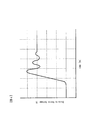
- FIG. 3 is a diagram illustrating an example of a simulation result of a dv / dt waveform at the time of switching when the capacitors 21a and 21b are provided in the switching circuit of FIG.
- FIG. 4 is a diagram illustrating an example of a simulation result of a dv / dt waveform at the time of switching when the capacitors 21a and 21b are not provided.
- the horizontal axis represents time
- the vertical axis represents the drain-source voltage. Comparing the dv / dt waveforms of FIGS. 3 and 4, the dv / dt waveform of FIG. 3 has a longer rise time than the dv / dt waveform of FIG. 4 and suppresses surge voltage and ringing. I understand that.
- the capacitance of the capacitors 21a and 21b in each switching circuit is such that the surge voltage generated between the drain and the source when the MOSFET 20 of the switching circuit is switched is less than a predetermined specified voltage, and the rise time is a predetermined specified value. Each is preferably set so that it is less than the time.
- the specified voltage and the specified time at this time can be determined based on required values of EMC performance and voltage conversion performance for the power supply device 1.
- the capacitances of the capacitors 21a and 21b in each switching circuit are set so that the voltage change characteristics (dv / dt characteristics) between the drain and source when the MOSFET 20 of each switching circuit is switched are within a predetermined range. , Each may be set. In this way, variation in the characteristics of the MOSFET 20 between the switching circuits can be suppressed, and the switching operation of each switching circuit can be controlled with high accuracy.
- the switching circuits SWA1 to SWA4 and SWB1 to SWB4 of the rectifier circuit 4 that are connected in parallel and operated simultaneously are improved in the simultaneity of these switching operations, so that higher output and higher efficiency can be achieved. Can be achieved.
- variable capacitance type capacitors may be used as the capacitors 21a and 21b.
- the variable capacitance type capacitors include those that mechanically change the area and distance of the opposing electrodes by rotating the adjusting rotation shaft, and varactor diodes that change the capacitance according to the reverse bias voltage. It is well known.
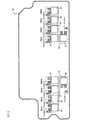
- FIG. 5 is a diagram showing an example of component arrangement of the MOSFETs 20 and capacitors 21a and 21b of the switching circuits S3 and S4, SWA1 to SWA4 and SWB1 to SWB4 in the rectifier circuit 4.
- each MOSFET 20 has a terminal pin for mounting on the substrate 30, and each capacitor 21 a, 21 b is arranged in the vicinity of the corresponding terminal pin of the MOSFET 20.
- the capacitors 21a and 21b of the switching circuits SWA1 to SWA4 and SWB1 to SWB4 are mounted side by side with the terminal pins at positions adjacent to the corresponding terminal pins of the MOSFET 20 on the substrate 30.
- the MOSFETs 20 of the switching circuits SWA2 to SWA4 and SWB2 to SWB4 are mounted on the substrate 30 with their terminal pins adjacent to each other.
- the capacitors 21 a and 21 b of these switching circuits are mounted on the substrate 30 between the terminal pins of the two MOSFETs 20 adjacent to each other. For example, such a component arrangement can effectively suppress surge voltage and ringing during switching.
- the power supply device 1 converts input DC power into AC power having a predetermined voltage and supplies it to the outside.
- the power supply device 1 is connected to the transformer 3 and the primary side of the transformer 3 and is input to the power supply device 1.
- DC / AC conversion circuit 2 that converts the converted DC power into AC power and outputs it to transformer 3; and rectifier circuit 4 that is connected to the secondary side of transformer 3 and converts AC power transformed by transformer 3 into DC power.
- the rectifying circuit 4 is electrically connected in parallel to each MOSFET 20 of the switching circuits SWA1 to SWA4 electrically connected in parallel to one end of the secondary side of the transformer 3 and to the other end of the secondary side of the transformer 3.
- MOSFETs 20 of the switching circuits SWB1 to SWB4 connected to each other and capacitors 21a and 21b electrically connected in parallel to each of these MOSFETs 20, respectively. Since it did in this way, the highly efficient and low noise power supply device 1 can be provided.
- the capacitances of the capacitors 21a and 21b are set so that the surge voltage generated when the corresponding MOSFET 20 is switched is less than a predetermined specified voltage and the rise time is less than a predetermined specified time. Is preferred. By doing in this way, the power supply device 1 which satisfy
- the capacitances of the capacitors 21a and 21b are set so that the voltage change characteristics when the MOSFETs 20 of the switching circuits SWA1 to SWA4 and SWB1 to SWB4 are respectively switched are within a predetermined range. May be. By doing so, the simultaneity of the switching operations of the switching circuits SWA1 to SWA4 and SWB1 to SWB4 can be improved, and the power supply device 1 can be further increased in output and efficiency.
- Each of the MOSFETs 20 of the switching circuits SWA1 to SWA4 and SWB1 to SWB4 has a terminal pin for mounting on the substrate 30, and each of the capacitors 21a and 21b of these switching circuits is on the substrate 30. It is mounted side by side with the terminal pin at a position adjacent to the terminal pin of the corresponding MOSFET 20. Further, the MOSFETs 20 of the switching circuits SWA2 to SWA4 and SWB2 to SWB4 are mounted on the substrate 30 with their terminal pins adjacent to each other, and the capacitors 21a and 21b of these switching circuits are adjacent to each other on the substrate 30. It is mounted between the terminal pins of the two MOSFETs 20. With such a component arrangement, surge voltage and ringing during switching can be effectively suppressed.
- a plurality of capacitors 21a and 21b electrically connected in series are provided for each MOSFET 20 of the switching circuits SWA1 to SWA4 and SWB1 to SWB4. Since it did in this way, the noise suppression effect can be maintained even when one of capacitors fails.
- the DC / AC conversion circuit 2 includes switching MOSFETs H1 and H2 connected to one end of the primary side of the transformer 3, and switching circuits H3 and H4 connected to the other end of the primary side of the transformer 3.
- MOSFET 20 and capacitors 21a and 21b electrically connected in parallel to each of MOSFET 20 are provided. Since it did in this way, the noise generated from the power supply device 1 can further be suppressed.
- the power supply device 1 that is a part of a power supply system mounted on a vehicle such as an electric vehicle or a hybrid vehicle has been described as an example, but a power supply device used for other purposes may be used.
- the present invention may be applied to a power supply device mounted on a normal automobile that travels using a gasoline engine or a diesel engine as a drive source, or other types of vehicles such as trains, or mounted on devices other than vehicles.
- the present invention may be applied to a power supply device.
Landscapes
- Engineering & Computer Science (AREA)
- Power Engineering (AREA)
- Dc-Dc Converters (AREA)
Abstract
高効率で低ノイズの電源装置を提供する。 電源装置は、トランス3と、トランス3の一次側に接続され、入力された直流電力を交流電力に変換してトランス3へ出力する直流交流変換回路2と、トランス3の二次側に接続され、トランス3により変圧された交流電力を直流電力に変換する整流回路4とを備える。整流回路4は、トランス3の二次側の一端に、互いに電気的に並列に接続されたスイッチング回路SWA1~SWA4の各MOSFET20と、トランス3の二次側の他端に、互いに電気的に並列に接続されたスイッチング回路SWB1~SWB4の各MOSFET20と、これらのMOSFET20の各々に対してそれぞれ電気的に並列に接続されたコンデンサ21a、21bとを有する。
Description
本発明は、入力された直流電力を所定電圧の直流電力に電圧変換する電源装置に関する。
従来、スイッチとトランスを用いて直流電力の電圧変換を行うスイッチング電源装置(DC/DCコンバータ)が知られている。このような電源装置において、トランスの二次側に設けられた整流回路内のスイッチをスイッチングさせる際に発生するサージ電圧を低減するために、スイッチと並列にスナバ用コンデンサを接続したものが提案されている(特許文献1)。
電源装置は、近年では電気自動車、プラグインハイブリッド電気自動車、燃料電池車等の車両に搭載され、モータ駆動用の高圧バッテリーからの直流電力を用いて補機用の低圧バッテリーを充電する際などに利用されている。こうした車両用の電源装置では、バッテリー容量の制限や、他の機器の動作への悪影響を防止する必要性などの理由により、高効率で低ノイズのものとすることが重要である。しかし、特許文献1に開示された電源装置では、この点について必ずしも十分ではない。
本発明による電源装置は、入力された直流電力を所定電圧の直流電力に電圧変換して外部へ供給するものであって、トランス回路と、トランス回路の一次側に接続され、入力された直流電力を交流電力に変換してトランス回路へ出力する直流交流変換回路と、トランス回路の二次側に接続され、トランス回路により変圧された交流電力を直流電力に変換する整流回路と、を備える。整流回路は、トランス回路の二次側の一端に、互いに電気的に並列に接続された複数の第1スイッチング素子と、トランス回路の二次側の他端に、互いに電気的に並列に接続された複数の第2スイッチング素子と、第1スイッチング素子および第2スイッチング素子の各々に対してそれぞれ電気的に並列に接続された複数のコンデンサ素子とを有する。
本発明によれば、高効率で低ノイズの電源装置を提供することができる。
以下に図面を参照して本発明の一実施形態による電源装置について説明する。図1は、本発明の一実施形態による電源装置を含む電源システムの構成を示すブロック図である。この電源システムは、たとえば電気自動車やハイブリッド自動車など、電気モータで駆動される車両に搭載されて使用される。
図1に示す電源システムは、電源装置1、補機バッテリー9、電装品10および高圧バッテリー11を有する。電源装置1および高圧バッテリー11は、導電性を有する金属製のケース111、121でそれぞれ覆われており、シールド線12a、12bを介して互いに接続されている。電源装置1のケース111は、金属製のボルト13a、13bにより車両のシャーシ8に固定されている。高圧バッテリー11のケース121も同様に、金属製のボルト13c、13dによりシャーシ8に固定されている。これにより、電源装置1および高圧バッテリー11がシャーシ8と電気的に接続され、共通の車両アースに接地される。
電源装置1は、直流交流変換回路2、トランス3、整流回路4および制御回路5を備えている。これらはケース111内に収納されており、ケース111の電位を共通のグランド(GND)電位として接地されている。ケース111には、接地用ケーブル7の一端に接続されている金属製のボルト13eが取り付けられている。接地用ケーブル7の他端は、シャーシ8に取り付けられた金属製のボルト13fと接続されている。このようにしてケース111とシャーシ8が接地用ケーブル7を介して電気的に接続されることで、前述のボルト13a、13bによる接地に加えて、ボルト13fが取り付けられているシャーシ8の部分を接地点として、さらに電源装置1の接地が行われている。
電源装置1には、シールド線12a、12bを介して高圧バッテリー11から入力される高電圧の直流電力を交流電力に変換する直流交流変換回路2と、直流交流変換回路2から出力された交流電力を変圧するトランス3と、トランス3にて変圧された交流電力を低電圧の直流電力に変換する整流回路3と、制御回路5とが設けられている。制御回路5は、直流交流変換回路2と整流回路4にそれぞれ設けられたスイッチング素子のオン/オフ制御を行うことで、これらの回路を同期して動作させ、上記のような電力変換を行わせる。これにより、電源装置1は、高圧バッテリー11から出力される高電圧の直流電力を低電圧の直流電力に電力変換し、その電圧変換後の直流電力を補機バッテリー9および電装品10へと出力することができる。
なお、電源装置1を双方向に電圧変換可能な構成としてもよい。この場合、補機バッテリー9や電装品10から入力される低電圧の直流電力を整流回路3により交流電力に変換し、その交流電力をトランス3により変圧した後、直流交流変換回路2で高電圧の直流電力に変換して高圧バッテリー11へ供給する。
整流回路4の(+)側出力は、ケース111に設けられた出力端子6を介して、補機バッテリー9および電装品10の(+)端子と接続されている。一方、整流回路4の(-)側出力は、ボルト13e、接地用ケーブル7およびボルト13fを介して、補機バッテリー9の(-)端子と接続されている。また、ボルト13e、接地用ケーブル7、ボルト13fおよびシャーシ8を介して、電装品10の(-)端子と接続されている。これにより、電源装置1を介して、高圧バッテリー11から補機バッテリー9および電装品10へ直流電力が供給される。
図2は、直流交流変換回路2、トランス3および整流回路4の回路構成の一例を示す回路図である。この回路構成において、トランス3の一次側、すなわち高電圧(HV)側には直流交流変換回路2が接続され、二次側、すなわち低電圧(LV)側には整流回路4が接続されている。図1の制御回路5の制御によりこれらの回路が協働して動作することで、高圧バッテリー11からHV(+)端子とHV(-)端子間に入力された高電圧の直流電力が直流交流変換回路2で交流電力へと変換され、トランス3で変圧された後、整流回路4で同期整流されて低電圧の直流電力に変換される。この変換後の低電圧の直流電力は、LV(+)端子とLV(-)端子間に接続された補機バッテリー9や電装品10へと出力される。なお、前述のように電源装置1を双方向に電圧変換可能な構成とした場合は、電力供給の方向に応じて、上記のような直流交流変換回路2と整流回路4の動作が互いに入れ替わる。
直流交流変換回路2には、スイッチング回路H1~H4で構成されたHブリッジ回路が設けられている。スイッチング回路H1、H2は、トランス3の一次側の一端に接続されており、スイッチング回路H3、H4は、トランス3の一次側の他端に接続されている。また整流回路4には、スイッチング回路S3、S4、SWA1~SWA4およびSWB1~SWB4で構成されたHブリッジ回路が設けられている。スイッチング回路S4およびSWA1~SWA4は、トランス3の二次側の一端に接続されており、スイッチング回路S3およびSWB1~SWB4は、トランス3の二次側の他端に接続されている。直流交流変換回路2および整流回路4におけるこれらのスイッチング回路のうち、たとえばスイッチング回路S4は、図中に示すように、還流ダイオードを有するスイッチング素子としてのMOSFET20と、コンデンサ21a、21bとによって構成されている。他のスイッチング回路についても同様の構成である。
直流交流変換回路2のHブリッジ回路において、各スイッチング回路H1~H4は、制御回路5からの制御信号に応じて、所定のスイッチング周波数(たとえば100kHz)でオンオフを交互に繰り返すスイッチング動作を行う。このHブリッジ回路からの出力は、インダクタLrとコンデンサCrによって構成されるLC回路を経由して、トランス3の一次側に入力される。そのため、HV(+)端子とHV(-)端子間に入力された直流電力が直流交流変換回路2においてゼロ電圧を中心にスイッチングされ、交流電力が生成される。これにより、スイッチング損失を低減して変換効率を向上することができる。
一方、整流回路4のHブリッジ回路における各スイッチング回路S3、S4、SWA1~SWA4およびSWB1~SWB4は、制御回路5からの制御信号に応じて、上記の直流交流変換回路2のHブリッジ回路と同期したスイッチング動作をそれぞれ行う。整流回路4では、このHブリッジ回路のスイッチング動作とインダクタL1、L2により、トランス3で変圧された交流電力が直流電力に変換され、LV(+)端子とLV(-)端子間に出力される。スイッチング回路SWA1~SWA4は互いに電気的に並列に接続されており、これらは同時にスイッチング動作を行う。また同様に、スイッチング回路SWB1~SWB4も互いに電気的に並列に接続されており、同時にスイッチング動作を行う。このような構成とすることで、整流回路4では高出力化、高効率化を実現している。
なお、図2の例では、スイッチング回路SWA1~SWA4、SWB1~SWB4をそれぞれ4つずつ電気的に並列に接続して整流回路4を構成しているが、並列するスイッチング回路の数はこれに限定されない。また、スイッチング回路S3、S4についても同様に、複数のスイッチング回路を並列させて構成してもよい。さらに、直流交流変換回路2のスイッチング回路H1~H4についても同様に、複数のスイッチング回路を並列させて構成することも可能である。
直流交流変換回路2および整流回路4の各スイッチング回路では、MOSFET20のドレイン-ソース間にコンデンサ21a、21bが接続されている。コンデンサ21a、21bは、各スイッチング回路の立ち上がり(Rate of Rise)特性、すなわちスイッチング時のドレイン-ソース間の電圧変化特性(dv/dt特性)を任意の条件に調整することを目的として、各スイッチング回路に設けられたものである。このコンデンサ21a、21bの容量を適切に設定することで、各スイッチング回路において所望のスイッチング速度を確保しつつ、スイッチング時のサージ電圧の発生を抑えることができる。その結果、電源装置1からのノイズ放出を抑制し、所望のEMC性能を得ることができる。
さらに、電気的に直列に接続された2つのコンデンサ21a、21bを各スイッチング回路に設けているため、いずれか一方のコンデンサが故障した場合にもノイズ抑制効果を保つことができる。なお、図2の例では、各スイッチング回路において2つのコンデンサ21a、21bを電気的に直列に接続することとしたが、接続するコンデンサの数はこれに限定されない。
図3は、図2のスイッチング回路でコンデンサ21a、21bがある場合のスイッチング時のdv/dt波形のシミュレーション結果の一例を示す図である。一方、図4は、コンデンサ21a、21bがない場合のスイッチング時のdv/dt波形のシミュレーション結果の一例を示す図である。これらの図では、横軸が時間を、縦軸がドレイン-ソース間電圧を表している。図3と図4のdv/dt波形を比較すると、図3のdv/dt波形では、図4のdv/dt波形に比べて立ち上がり時間が長くなっており、サージ電圧やリンギングが抑制されていることが分かる。
なお、各スイッチング回路におけるコンデンサ21a、21bの容量は、当該スイッチング回路のMOSFET20をスイッチングさせたときにドレイン-ソース間に生じるサージ電圧が所定の規定電圧未満であり、かつ、立ち上がり時間が所定の規定時間未満となるように、それぞれ設定されることが好ましい。このときの規定電圧や規定時間は、電源装置1に対するEMC性能や電圧変換性能の要求値等に基づいて定めることができる。
また、各スイッチング回路におけるコンデンサ21a、21bの容量を、各スイッチング回路のMOSFET20をスイッチングさせたときのドレイン-ソース間の電圧変化特性(dv/dt特性)がいずれも所定の範囲内となるように、それぞれ設定してもよい。このようにすれば、各スイッチング回路間でのMOSFET20の特性のばらつきを抑え、各スイッチング回路のスイッチング動作を高精度に制御することができる。特に、並列に接続されており同時にスイッチング動作される整流回路4のスイッチング回路SWA1~SWA4およびSWB1~SWB4については、これらのスイッチング動作の同時性が向上されるため、さらなる高出力化や高効率化を図ることができる。
以上説明したような容量設定を容易に実現できるようにするため、コンデンサ21a、21bとして可変容量型のコンデンサを用いてもよい。可変容量型のコンデンサとしては、たとえば、調整用の回転軸を回転させることで対向する電極の面積や距離を機械的に変化させるものや、逆バイアス電圧に応じて容量を変化させるバラクタダイオード等が周知である。
図5は、整流回路4におけるスイッチング回路S3、S4、SWA1~SWA4およびSWB1~SWB4の各MOSFET20および各コンデンサ21a、21bの部品配置例を示す図である。この図に示すように、各MOSFET20は基板30に実装するための端子ピンをそれぞれ有しており、各コンデンサ21a、21bは対応するMOSFET20の端子ピンの近傍に配置されている。特に、スイッチング回路SWA1~SWA4およびSWB1~SWB4の各コンデンサ21a、21bは、基板30上で、対応するMOSFET20の端子ピンと隣接した位置に、当該端子ピンと並べて実装されている。また、スイッチング回路SWA2~SWA4およびSWB2~SWB4の各MOSFET20は、端子ピン同士が互いに隣接して基板30に実装されている。これらのスイッチング回路の各コンデンサ21a、21bは、基板30上で、互いに隣接する2つのMOSFET20の端子ピンと端子ピンの間に実装されている。たとえばこのような部品配置とすることで、スイッチング時のサージ電圧やリンギングを効果的に抑制することができる。
以上説明した実施の形態によれば、次の作用効果を奏する。
(1)電源装置1は、入力された直流電力を所定電圧の交流電力に電圧変換して外部へ供給するものであり、トランス3と、トランス3の一次側に接続され、電源装置1に入力された直流電力を交流電力に変換してトランス3へ出力する直流交流変換回路2と、トランス3の二次側に接続され、トランス3により変圧された交流電力を直流電力に変換する整流回路4とを備える。整流回路4は、トランス3の二次側の一端に、互いに電気的に並列に接続されたスイッチング回路SWA1~SWA4の各MOSFET20と、トランス3の二次側の他端に、互いに電気的に並列に接続されたスイッチング回路SWB1~SWB4の各MOSFET20と、これらのMOSFET20の各々に対してそれぞれ電気的に並列に接続されたコンデンサ21a、21bとを有する。このようにしたので、高効率で低ノイズの電源装置1を提供することができる。
(2)コンデンサ21a、21bの容量は、対応するMOSFET20をスイッチングさせたときに生じるサージ電圧が所定の規定電圧未満であり、かつ、立ち上がり時間が所定の規定時間未満となるように設定されることが好ましい。このようにすることで、所望のEMC性能や電圧変換性能を満たす電源装置1を実現できる。
(3)また、コンデンサ21a、21bの容量は、スイッチング回路SWA1~SWA4およびSWB1~SWB4の各MOSFET20をそれぞれスイッチングさせたときの電圧変化特性がいずれも所定の範囲内となるように、それぞれ設定されてもよい。このようにすることで、スイッチング回路SWA1~SWA4およびSWB1~SWB4のスイッチング動作の同時性を向上して、電源装置1のさらなる高出力化や高効率化を図ることができる。
(4)スイッチング回路SWA1~SWA4およびSWB1~SWB4の各MOSFET20は、基板30に実装するための端子ピンをそれぞれ有しており、これらのスイッチング回路の各コンデンサ21a、21bは、基板30上で、対応するMOSFET20の端子ピンと隣接した位置に、当該端子ピンと並べて実装される。さらに、スイッチング回路SWA2~SWA4およびSWB2~SWB4の各MOSFET20は、端子ピン同士が互いに隣接して基板30に実装され、これらのスイッチング回路の各コンデンサ21a、21bは、基板30上で、互いに隣接する2つのMOSFET20の端子ピンと端子ピンの間に実装される。このような部品配置とすることで、スイッチング時のサージ電圧やリンギングを効果的に抑制することができる。
(5)スイッチング回路SWA1~SWA4およびSWB1~SWB4の各MOSFET20に対して、電気的に直列にされた複数のコンデンサ21a、21bがそれぞれ設けられている。このようにしたので、いずれかのコンデンサが故障した場合にもノイズ抑制効果を保つことができる。
(6)直流交流変換回路2は、トランス3の一次側の一端に接続されたスイッチング回路H1、H2の各MOSFET20と、トランス3の一次側の他端に接続されたスイッチング回路H3、H4の各MOSFET20と、これらのMOSFET20の各々に対してそれぞれ電気的に並列に接続されたコンデンサ21a、21bとを有する。このようにしたので、電源装置1から発生されるノイズをさらに抑制することができる。
以上、本発明の一実施形態を詳細に説明したが、本発明は上述の実施形態に限定されるものではなく、技術思想の範囲内で適宜変更可能である。たとえば、上記実施形態では、電気自動車やハイブリッド自動車等の車両に搭載される電源システムの一部である電源装置1を例として説明したが、これ以外の用途に用いる電源装置であってもよい。たとえば、ガソリンエンジンやディーゼルエンジンを駆動源として走行する通常の自動車や、電車等の他の種類の車両に搭載される電源装置に本発明を適用してもよいし、車両以外のものに搭載される電源装置に本発明を適用してもよい。
以上説明した実施形態や各種の変形例はあくまで一例であり、発明の特徴が損なわれない限り、本発明はこれらの内容に限定されるものではない。
1 電源装置
2 直流交流変換回路
3 トランス
4 整流回路
5 制御回路
20 MOSFET
21a、21b コンデンサ
2 直流交流変換回路
3 トランス
4 整流回路
5 制御回路
20 MOSFET
21a、21b コンデンサ
Claims (7)
- 入力された直流電力を所定電圧の直流電力に電圧変換して外部へ供給する電源装置であって、
トランス回路と、
前記トランス回路の一次側に接続され、前記入力された直流電力を交流電力に変換して前記トランス回路へ出力する直流交流変換回路と、
前記トランス回路の二次側に接続され、前記トランス回路により変圧された交流電力を直流電力に変換する整流回路と、を備え、
前記整流回路は、
前記トランス回路の二次側の一端に、互いに電気的に並列に接続された複数の第1スイッチング素子と、
前記トランス回路の二次側の他端に、互いに電気的に並列に接続された複数の第2スイッチング素子と、
前記第1スイッチング素子および前記第2スイッチング素子の各々に対してそれぞれ電気的に並列に接続された複数のコンデンサ素子とを有することを特徴とする電源装置。 - 請求項1に記載の電源装置において、
前記コンデンサ素子の容量は、対応する前記第1スイッチング素子または前記第2スイッチング素子をスイッチングさせたときに生じるサージ電圧が所定の規定電圧未満であり、かつ、立ち上がり時間が所定の規定時間未満となるように設定されることを特徴とする電源装置。 - 請求項1または2に記載の電源装置において、
前記複数のコンデンサ素子の容量は、前記複数の第1スイッチング素子および前記複数の第2スイッチング素子をそれぞれスイッチングさせたときの電圧変化特性がいずれも所定の範囲内となるように、それぞれ設定されることを特徴とする電源装置。 - 請求項1または2に記載の電源装置において、
前記第1スイッチング素子および前記第2スイッチング素子は、基板に実装するための端子ピンをそれぞれ有し、
前記コンデンサ素子は、前記基板上で、対応する前記第1スイッチング素子または前記第2スイッチング素子の前記端子ピンと隣接した位置に、当該端子ピンと並べて実装されることを特徴とする電源装置。 - 請求項4に記載の電源装置において、
前記第1スイッチング素子および前記第2スイッチング素子のうちいずれか少なくとも2つは、前記端子ピン同士が互いに隣接して前記基板に実装され、
前記コンデンサ素子は、前記基板上で、互いに隣接する前記端子ピンと前記端子ピンの間に実装されることを特徴とする電源装置。 - 請求項1または2に記載の電源装置において、
前記第1スイッチング素子および前記第2スイッチング素子の各々に対して、電気的に直列に接続された複数の前記コンデンサ素子がそれぞれ設けられていることを特徴とする電源装置。 - 請求項1または2に記載の電源装置において、
前記直流交流変換回路は、
前記トランス回路の一次側の一端に接続された第3スイッチング素子と、
前記トランス回路の一次側の他端に接続された第4スイッチング素子と、
前記第3スイッチング素子および前記第4スイッチング素子の各々に対してそれぞれ電気的に並列に接続された複数の一次側コンデンサ素子とを有することを特徴とする電源装置。
Applications Claiming Priority (2)
| Application Number | Priority Date | Filing Date | Title |
|---|---|---|---|
| JP2012-162863 | 2012-07-23 | ||
| JP2012162863A JP2014023391A (ja) | 2012-07-23 | 2012-07-23 | 電源装置 |
Publications (1)
| Publication Number | Publication Date |
|---|---|
| WO2014017253A1 true WO2014017253A1 (ja) | 2014-01-30 |
Family
ID=49997069
Family Applications (1)
| Application Number | Title | Priority Date | Filing Date |
|---|---|---|---|
| PCT/JP2013/067764 Ceased WO2014017253A1 (ja) | 2012-07-23 | 2013-06-28 | 電源装置 |
Country Status (2)
| Country | Link |
|---|---|
| JP (1) | JP2014023391A (ja) |
| WO (1) | WO2014017253A1 (ja) |
Citations (4)
| Publication number | Priority date | Publication date | Assignee | Title |
|---|---|---|---|---|
| JP2004281462A (ja) * | 2003-03-12 | 2004-10-07 | Toshiba Corp | 電力用半導体装置 |
| JP2006187147A (ja) * | 2004-12-28 | 2006-07-13 | Hitachi Ltd | 双方向絶縁型dc−dcコンバータ |
| JP2008271752A (ja) * | 2007-04-24 | 2008-11-06 | Kawamura Electric Inc | フルブリッジ回路の配線構造 |
| JP2012100490A (ja) * | 2010-11-04 | 2012-05-24 | Kawasaki Heavy Ind Ltd | 共振スイッチを用いた降圧チョッパおよび電力供給システム |
Family Cites Families (1)
| Publication number | Priority date | Publication date | Assignee | Title |
|---|---|---|---|---|
| JP2567015Y2 (ja) * | 1991-10-08 | 1998-03-30 | 松下電工株式会社 | インバータ装置 |
-
2012
- 2012-07-23 JP JP2012162863A patent/JP2014023391A/ja active Pending
-
2013
- 2013-06-28 WO PCT/JP2013/067764 patent/WO2014017253A1/ja not_active Ceased
Patent Citations (4)
| Publication number | Priority date | Publication date | Assignee | Title |
|---|---|---|---|---|
| JP2004281462A (ja) * | 2003-03-12 | 2004-10-07 | Toshiba Corp | 電力用半導体装置 |
| JP2006187147A (ja) * | 2004-12-28 | 2006-07-13 | Hitachi Ltd | 双方向絶縁型dc−dcコンバータ |
| JP2008271752A (ja) * | 2007-04-24 | 2008-11-06 | Kawamura Electric Inc | フルブリッジ回路の配線構造 |
| JP2012100490A (ja) * | 2010-11-04 | 2012-05-24 | Kawasaki Heavy Ind Ltd | 共振スイッチを用いた降圧チョッパおよび電力供給システム |
Also Published As
| Publication number | Publication date |
|---|---|
| JP2014023391A (ja) | 2014-02-03 |
Similar Documents
| Publication | Publication Date | Title |
|---|---|---|
| EP2849308B1 (en) | Motor drive device | |
| US20200007026A1 (en) | Power converter | |
| US9729042B2 (en) | Power supply apparatus for power converters | |
| CN112224057B (zh) | 一种车辆及其能量转换装置与动力系统 | |
| JP2011120440A (ja) | 電力変換装置 | |
| US11018572B2 (en) | Inverter with intermediate circuit capacitor cascade and DC-side common-mode and differential-mode filters | |
| JP6471656B2 (ja) | インバータ制御基板 | |
| CN106849714B (zh) | 功率转换装置 | |
| CN107681884B (zh) | 一种汽车空调压缩机及汽车 | |
| CN111095767A (zh) | 驱动电源装置 | |
| CN112838750B (zh) | 有源共模抵消 | |
| JP6731673B2 (ja) | 双方向チョッパ回路 | |
| CN112352374A (zh) | 开关电源装置及包括该开关电源装置的车载用电动压缩机 | |
| JP6953634B2 (ja) | Dc/dcコンバータを備える車両充電器 | |
| JP7003449B2 (ja) | 車載装置 | |
| WO2018078734A1 (ja) | 電力変換装置 | |
| JP2014023391A (ja) | 電源装置 | |
| KR20160046416A (ko) | 노이즈 보상 회로 | |
| JPH09168208A (ja) | 電気自動車の電気システム | |
| JP5272593B2 (ja) | 電動機駆動システムおよびそれを備えた車両 | |
| JPH09168205A (ja) | ハイブリッド電気自動車の電気システム | |
| JP6222685B2 (ja) | 回路基板 | |
| JP7580494B2 (ja) | 変圧装置 | |
| HK1252510A1 (zh) | 带有缓冲器电路的电功率转换器 | |
| KR20260029140A (ko) | 모터 구동 장치 및 이를 포함하는 전동화 차량 |
Legal Events
| Date | Code | Title | Description |
|---|---|---|---|
| 121 | Ep: the epo has been informed by wipo that ep was designated in this application |
Ref document number: 13822893 Country of ref document: EP Kind code of ref document: A1 |
|
| NENP | Non-entry into the national phase |
Ref country code: DE |
|
| 122 | Ep: pct application non-entry in european phase |
Ref document number: 13822893 Country of ref document: EP Kind code of ref document: A1 |