WO2014017242A1 - 有機エレクトロルミネッセンス素子 - Google Patents
有機エレクトロルミネッセンス素子 Download PDFInfo
- Publication number
- WO2014017242A1 WO2014017242A1 PCT/JP2013/067495 JP2013067495W WO2014017242A1 WO 2014017242 A1 WO2014017242 A1 WO 2014017242A1 JP 2013067495 W JP2013067495 W JP 2013067495W WO 2014017242 A1 WO2014017242 A1 WO 2014017242A1
- Authority
- WO
- WIPO (PCT)
- Prior art keywords
- organic
- layer
- light
- glass cloth
- sheet
- Prior art date
- Legal status (The legal status is an assumption and is not a legal conclusion. Google has not performed a legal analysis and makes no representation as to the accuracy of the status listed.)
- Ceased
Links
Images

Classifications
-
- H—ELECTRICITY
- H10—SEMICONDUCTOR DEVICES; ELECTRIC SOLID-STATE DEVICES NOT OTHERWISE PROVIDED FOR
- H10K—ORGANIC ELECTRIC SOLID-STATE DEVICES
- H10K50/00—Organic light-emitting devices
- H10K50/80—Constructional details
- H10K50/85—Arrangements for extracting light from the devices
- H10K50/858—Arrangements for extracting light from the devices comprising refractive means, e.g. lenses
-
- H—ELECTRICITY
- H10—SEMICONDUCTOR DEVICES; ELECTRIC SOLID-STATE DEVICES NOT OTHERWISE PROVIDED FOR
- H10K—ORGANIC ELECTRIC SOLID-STATE DEVICES
- H10K50/00—Organic light-emitting devices
- H10K50/80—Constructional details
- H10K50/805—Electrodes
- H10K50/81—Anodes
-
- H—ELECTRICITY
- H10—SEMICONDUCTOR DEVICES; ELECTRIC SOLID-STATE DEVICES NOT OTHERWISE PROVIDED FOR
- H10K—ORGANIC ELECTRIC SOLID-STATE DEVICES
- H10K50/00—Organic light-emitting devices
- H10K50/80—Constructional details
- H10K50/805—Electrodes
- H10K50/82—Cathodes
-
- H—ELECTRICITY
- H10—SEMICONDUCTOR DEVICES; ELECTRIC SOLID-STATE DEVICES NOT OTHERWISE PROVIDED FOR
- H10K—ORGANIC ELECTRIC SOLID-STATE DEVICES
- H10K50/00—Organic light-emitting devices
- H10K50/80—Constructional details
- H10K50/85—Arrangements for extracting light from the devices
-
- H—ELECTRICITY
- H10—SEMICONDUCTOR DEVICES; ELECTRIC SOLID-STATE DEVICES NOT OTHERWISE PROVIDED FOR
- H10K—ORGANIC ELECTRIC SOLID-STATE DEVICES
- H10K50/00—Organic light-emitting devices
- H10K50/80—Constructional details
- H10K50/84—Passivation; Containers; Encapsulations
- H10K50/844—Encapsulations
-
- H—ELECTRICITY
- H10—SEMICONDUCTOR DEVICES; ELECTRIC SOLID-STATE DEVICES NOT OTHERWISE PROVIDED FOR
- H10K—ORGANIC ELECTRIC SOLID-STATE DEVICES
- H10K50/00—Organic light-emitting devices
- H10K50/80—Constructional details
- H10K50/85—Arrangements for extracting light from the devices
- H10K50/854—Arrangements for extracting light from the devices comprising scattering means
Definitions
- the present invention relates to an organic electroluminescence element applicable to, for example, a display, a lighting fixture, and the like.
- Illumination (organic EL illumination) using an organic electroluminescence (EL) element is a self-luminous illumination device. Therefore, organic EL illumination has been actively researched and developed for use in various displays, backlights for liquid crystal displays, flat illumination, and the like.
- display devices using organic EL elements have superior visibility and independence of viewing angle compared to cathode ray tube displays (Cathode Ray Tube; CRT) and liquid crystal displays. Has performance.
- the organic EL display has an advantage that it can be reduced in weight and thickness.
- organic EL illumination is a uniform surface light source, unlike LED illumination using LED (Light Emitting Diode) which is a highly directional point light source. For this reason, organic EL lighting has the advantage that it can be made thin and lightweight, and the number of parts can be reduced. Further, in organic EL lighting, by using a flexible substrate, there is a possibility that lighting having a shape that has been difficult to realize in the past can be realized.
- LED Light Emitting Diode
- Organic EL lighting is composed of a plurality of members.
- the organic EL illumination is formed as an organic EL surface light emitter by providing an anode, an organic light emitting layer, a cathode, and the like in this order on one surface of a transparent substrate.
- the organic light emitting layer emits light.
- the light emitted from the organic light emitting layer is emitted to the outside through a plurality of members such as a transparent substrate.
- the emitted light When the light emitted from the organic light emitting layer is emitted to the outside, the emitted light may be totally reflected depending on the incident angle to the adjacent layer interface having a different refractive index, and may be guided inside the display device. . When this phenomenon occurs, the emitted light is not emitted to the outside. That is, the emitted light may be attenuated by total reflection or the like due to a difference in refractive index between members, and may not be efficiently emitted to the outside.
- the surface illumination device described in Patent Document 1 includes an optical sheet having a condensing function, and the optical sheet has a condensing function.
- This optical sheet has, for example, a transparent substrate layer and an optical layer in which beads are dispersed in a binder.
- the optical film described in Patent Document 2 has a concavo-convex structure portion, and this concavo-convex structure portion has a concavo-convex structure formed on one surface, and the surface on the concavo-convex structure side of the concavo-convex structure portion has an uneven structure. It has a shape formed by repeatedly arranging unit shapes in at least one direction along the surface of the concavo-convex structure side.
- Patent Documents 1 and 2 do not consider weather resistance against solar heat, sunlight, and the like. Therefore, when the optical sheet and optical film of patent documents 1 and 2 are applied and the organic EL element which improved the light extraction efficiency was produced, it is possible that the weather resistance of an organic EL element is not enough. When such an organic EL element having insufficient weather resistance is used, the organic EL element may deteriorate over time. In particular, when such an organic EL element is used, for example, for illumination installed outdoors, this aging deterioration becomes larger.
- the optical sheet or the optical film is caused by discoloration by heat or light.
- the luminance of the organic EL element may be reduced (that is, the light extraction efficiency may be reduced).
- the present invention has been made in view of the above circumstances, and a problem to be solved by the present invention is to provide an organic EL device that achieves both good light extraction efficiency and excellent weather resistance.
- the present inventor found that the above problems can be solved by providing a light extraction member including a glass cloth with respect to the organic EL element main body that emits light, and completed the present invention. . That is, the gist of the present invention is as follows.
- An organic electroluminescence element body comprising an electrode composed of an anode and a cathode, and an organic compound layer disposed between the anode and the cathode and emitting light when a voltage is applied between the electrodes;
- a light extraction member including at least one of the anode and the cathode, provided outside the electrode through which light emitted from the organic compound layer is transmitted, and including a glass cloth.
- an organic EL element that achieves both good light extraction efficiency and excellent weather resistance.
- the organic EL device of this embodiment includes an electrode composed of an anode and a cathode, and an organic compound layer that is disposed between the anode and the cathode and emits light when a voltage is applied between the electrodes.
- FIG. 1 is an example of the organic EL element of the present embodiment, and can be arbitrarily changed and implemented without departing from the gist of the present invention.
- the organic EL element 10 of the present embodiment includes an organic EL element body 1 and a sealing material 3 laminated in this order on a glass cloth sheet 2 (light extraction member). Yes.
- the glass cloth sheet 2 and the organic EL element body 1 are bonded and fixed by an adhesive layer 4 (formed by applying an adhesive).
- the organic EL element body 1 and the sealing material 3 are both bonded and fixed by the adhesive layer 4.
- the glass cloth sheet 2 provided in the organic EL element 10 of the present embodiment will be described. Thereafter, members other than the glass cloth sheet 2 provided in the organic EL element 10 of the present embodiment will be described.
- a glass cloth sheet 2 (light extraction member, hereinafter simply referred to as “sheet 2”) provided in the organic EL element 10 is an electrode through which light emitted from the organic compound layer 13 described later is transmitted (shown in FIG. 1).
- the organic EL element 10 is provided outside the anode 12) and includes a glass cloth.
- the shape of the light extraction member is not limited to a sheet shape, and may be a flat plate shape, for example.
- the sheet 2 is usually formed by adhering a glass cloth substrate 2a made of glass cloth and a light diffusion sheet 2b formed on the surface opposite to the surface on which the organic EL element body 1 is provided. Become.
- the glass cloth substrate 2a is made of glass cloth.
- the glass cloth is formed by weaving (woven) glass fibers. There are no particular limitations on the specific configuration, type, additives, and the like of such a glass cloth, and any glass cloth can be applied. However, the glass cloth is usually preferably colorless.
- the glass cloth applicable to the glass cloth base material 2a may be a commercially available one, or may be appropriately prepared. Moreover, 1 type of glass cloth may be used independently and 2 or more types may be used in arbitrary combinations.
- the glass cloth a glass cloth raw machine, a glass cloth subjected to various processing treatments, a used glass cloth, etc. can be applied.
- a glass cloth a glass cloth that has been subjected to a processing treatment is preferable. Specifically, a glass cloth that has been heat-cleaned or a glass cloth that has been heat-cleaned and then treated with a silane coupling agent is more preferable. Details of these glass cloths will be described later.
- any glass fiber used for the glass cloth may be used.
- the glass fiber include glass fibers such as E glass, D glass, T glass, C glass, ECR glass, A glass, L glass, S glass, YM31-A glass, and H glass. One of these may be used alone, or two or more of these may be used in any combination. Among these, E glass fiber is preferable. These glass fibers may be produced according to an arbitrary production method, or commercially available products may be used.
- the glass fiber may consist of either a long fiber or a short fiber.
- the glass fiber is a long fiber, for example, a glass fiber that is appropriately drawn and hardened can be used. In this case, however, the glass fiber is preferably twisted.
- the number of twists is not particularly limited, but for example, a twist of 20 to 200 times per 100 cm can be used.
- the twist direction may be either right twist (S twist) or left twist (Z twist).
- S twist right twist
- Z twist left twist
- a twisted yarn for example, a single twisted yarn, various twisted yarns, a bitco various twisted yarn, a strong twisted yarn, a wall twisted yarn, and a piece twisted yarn can be mentioned.
- the glass fiber is a short fiber, for example, a yarn obtained by twisting the glass fiber and joining them, that is, a spun yarn can be used.
- the degree of twisting the same matters as in the case of long fibers can be applied.
- the count of the glass fiber is not particularly limited, but is usually 1 tex or more, preferably 5 tex or more, and usually 1000 tex or less, preferably 850 tex or less, more preferably 200 tex or less, and particularly preferably 150 tex or less.
- any method can be applied as a method for weaving glass cloth (weaving method).
- the weaving include plain weaving, twill weaving, oblique weaving, tangle weaving, satin weaving, triaxial weaving, and horizontal stripe weaving.
- the weaving can be performed using a loom such as a jet loom (for example, an air jet loom, a water jet loom), a sulzer loom, a lepier loom, or the like. Weaving may be performed by appropriately combining these.
- the density of glass fibers in the formed glass cloth is not particularly limited. However, it is preferable that 10 or more glass fibers intersect each other in a 25 mm square glass cloth, and 40 or more are more preferable for this density when both warp and weft are used. Moreover, 80 or less are preferable and 60 or less are more preferable. By setting the density of the glass fibers within this range, the gap of the glass cloth can be reduced and sufficient tensile strength can be obtained. Moreover, the flexibility and softness of the glass cloth can be made sufficient, and the handleability can be improved.
- the light diffusion sheet 2b constituting the sheet 2 is provided on the surface of the glass cloth substrate 2a.
- the light diffusion sheet 2b may be provided only on one side of the glass cloth substrate 2a, or may be provided on both sides. Further, the light diffusion sheet 2b can be omitted. Further, for example, the glass cloth substrate 2a and the light diffusion sheet 2b may be integrally formed by impregnating a glass cloth with a component constituting the light diffusion sheet.
- the specific type of the light diffusion sheet 2b is not particularly limited, and for example, inorganic resin (silica or the like), vinyl chloride resin, vinyl ester resin, acrylic resin, or the like is applicable.
- inorganic resin silicon or the like
- vinyl chloride resin vinyl ester resin
- acrylic resin acrylic resin
- additives such as saccharides (monosaccharides, oligosaccharides, polysaccharides, etc.) may be included.
- the monosaccharide itself may be contained from the beginning, or a monosaccharide produced by a polysaccharide degrading enzyme added together with an oligosaccharide or a polysaccharide may be contained.
- saccharide examples include cyclodextrin, chitosan, pullulan and the like. One of these may be used alone, or two or more thereof may be used in any ratio and combination.
- the polysaccharide-degrading enzyme may be, for example, a glycosyltransferase (for example, cyclodextrin glucosyltransferase) in addition to an enzyme that decomposes a polysaccharide into a monosaccharide (for example, chitosanase, pullulanase, amylase, etc.).
- the physical properties of the sheet 2 are not particularly limited.
- the haze value of the sheet 2 is preferably 90% or more, more preferably 93% or more, still more preferably 95% or more, and particularly preferably 97% or more. By setting the haze value within this range, better light extraction efficiency can be achieved.
- the haze value (cloudiness value) can be calculated using the following formula (1).
- Haze value (%) ⁇ diffuse transmittance (%) / total light transmittance (%) ⁇ ⁇ 100 (1)
- the haze value can be measured by the method described in JIS-K-7136 “Plastics—Determination of haze for transparent materials” or ISO14782 “Plastics-Determination of haze for transparent materials”.
- the total light transmittance (total light transmittance) of the sheet 2 is preferably 40% or more, more preferably 41% or more, and particularly preferably 44% or more. By setting the total light transmittance within this range, better light extraction efficiency can be achieved.
- the total light transmittance is described in JIS-K-7361-1 “Testing method of total light transmittance of plastic-transparent material” or ISO 13468-1 “Plastics-Determinationeterof the total luminous transmittance of transparent materials”. It can be measured by the method that has been.
- the thickness of the sheet 2 can be, for example, 0.1 mm or more and 0.5 mm or less. By setting the thickness of the sheet 2 within this range, an organic EL element with better weather resistance, flexibility, and light extraction efficiency can be produced.
- seat 2 can be 100 g or more and 500 g or less as a mass per 1 m ⁇ 2 >, for example.
- an organic EL element with better weather resistance, flexibility, and light extraction efficiency can be produced.
- the organic EL element 10 of the present embodiment includes the sheet 2 including a glass cloth.
- the organic EL element 10 of the present embodiment includes the organic EL element body 1, the sealing material 3, and the adhesive layer 4 shown in FIG. 1.
- the sealing material 3 and the adhesive layer 4 may not be provided as appropriate.
- the extraction direction of the emitted light is not limited to this, and it may be extracted from the cathode side 14 or may be extracted from both the anode 12 and the cathode 14 side.
- the sheet 2 may be provided as appropriate, for example, on the light extraction surface on the cathode 14 side, depending on the direction in which the light is known. That is, when light is extracted from the cathode 14 side, the sheet 2 may be provided outside the cathode 14. When light is extracted from both sides of the anode 12 and the cathode 14, the sheet 2 may be provided on both sides of the outside of the anode 12 and the outside of the cathode 14.
- Organic EL element body 1 is an organic compound layer that is disposed between an electrode composed of an anode 12 and a cathode 14 and an anode 12 and a cathode 14 and emits light when a voltage is applied between the electrodes (the anode 12 and the cathode 14). 13.
- the light extracted from the organic EL element 10 is usually light emitted from the organic EL element body 1.
- the organic EL element body 1 usually includes various organic layers such as a carrier (hole and electron) injection layer, a blocking layer, and a transport layer, in addition to a light emitting layer that directly participates in light emission.
- the organic EL element main-body part 1 is normally comprised by laminating
- an element substrate 11, an anode 12, an organic compound layer 13 (such as a light emitting layer) and a cathode 14 are laminated to form the organic EL element body 1.
- a preferable stacking example in the organic compound layer 13 is as follows.
- the layers described above are usually provided on the positive electrode side, and are then laminated on the cathode side in the order described below.
- each part which comprises the organic EL element main-body part 1 is demonstrated.
- the configuration of the organic EL element body 1 is not limited to the following contents.
- the element substrate 11 (base, substrate, base, support, etc.) can be formed of a transparent material such as glass or plastic.
- the element substrate 11 is preferably composed of a flexible base material such as a thin film glass or a transparent resin film.
- the element substrate 11 is preferably made of a transparent resin material. Therefore, the element substrate 11 is preferably composed of a transparent resin film.
- transparent resin films examples include polyesters such as polyethylene terephthalate (PET) and polyethylene naphthalate (PEN), polyethylene, polypropylene, cellophane (registered trademark), cellulose diacetate, cellulose triacetate, cellulose acetate butyrate, and cellulose acetate propio.
- PET polyethylene terephthalate
- PEN polyethylene naphthalate
- polyethylene polypropylene
- cellophane registered trademark
- cellulose diacetate cellulose triacetate
- cellulose acetate butyrate examples include cellulose acetate propio.
- Cellulose esters such as nate (CAP), cellulose acetate phthalate (TAC), cellulose nitrate or derivatives thereof, polyvinylidene chloride, polyvinyl alcohol, polyethylene vinyl alcohol, syndiotactic polystyrene, polycarbonate, norbornene resin, polymethylpentene, Polyether ketone, polyimide, polyether sulfone (PES), polyphenylene sulfide, Resulfones, polyetherimide, polyetherketoneimide, polyamide, fluororesin, nylon (registered trademark), polymethyl methacrylate, acrylic or polyarylates, Arton (registered trademark, manufactured by JSR) or Appel (registered trademark, Mitsui Chemicals) And cycloolefin-based resins.
- CAP nate
- TAC cellulose acetate phthalate
- cellulose nitrate or derivatives thereof polyvinylidene chloride
- polyvinyl alcohol polyethylene
- the gas barrier layer mentioned later is formed in the surface of a transparent resin film.
- Gas barrier layer It is preferable that one or two or more gas barrier layers are formed between the element substrate 11 and the organic compound layer 12 from the viewpoint of moisture resistance. In FIG. 1, the gas barrier layer is not shown.
- the gas barrier layer examples include an inorganic film, an organic film, or a hybrid film of both.
- the water vapor permeability is preferably 0.01 g / (m 2 ⁇ day ⁇ 1013 hPa) or less.
- a high barrier film having an oxygen permeability of 10 ⁇ 3 ml / (m 2 ⁇ day) or less and a water vapor permeability of 10 ⁇ 5 g / (m 2 ⁇ day) or less is preferable.
- the material for forming the gas barrier layer is not particularly limited, but is preferably a material having a function of suppressing intrusion of elements that cause deterioration of elements such as moisture and oxygen.
- metal oxides such as silicon oxide and silicon dioxide, nitriding
- a metal nitride such as silicon can be used.
- the method for forming the gas barrier layer is not particularly limited.
- a vacuum deposition method for example, a vacuum deposition method, a sputtering method, a reactive sputtering method, a molecular beam epitaxy method, a cluster ion beam method, an ion plating method, a plasma polymerization method, an atmospheric pressure plasma polymerization method.
- a plasma CVD (Chemical Vapor Deposition) method, a laser CVD method, a thermal CVD method, a coating method, or the like can be used.
- the anode 12 is an electrode film that supplies (injects) holes to the organic compound layer 1 (specifically, the light emitting layer).
- the type and physical properties of the anode 12 are not particularly limited and can be arbitrarily set.
- the anode 12 has a high work function (4 eV or more) and can be formed of an electrode material such as a metal, an alloy, an electrically conductive compound, and a mixture thereof.
- the anode 12 may be made of a light-transmitting material (transparent electrode) such as indium tin oxide or indium zinc oxide.
- the refractive index of the anode 12 is arbitrary, but is preferably 1.5 or more, more preferably 1.55 or more, and is preferably 2 or less, more preferably 1.85 or less.
- the sheet resistance (surface resistance) of the anode 12 is arbitrary, but several hundred ⁇ / sq. The following values are preferred.
- the film thickness of the anode 12 is also arbitrary, and since it varies depending on the material to be formed, it cannot be generally stated, but is usually 10 nm or more, and usually 1000 nm or less, preferably 200 nm or less.
- the organic compound layer 13 generally includes various organic layers such as a carrier (hole and electron) injection layer, a blocking layer, and a transport layer in addition to the light emitting layer.
- a carrier hole and electron
- a blocking layer blocking layer
- a transport layer transport layer in addition to the light emitting layer.
- the light-emitting layer is injected directly from the anode 12 or from the anode 12 via the hole transport layer and the like, and directly from the cathode 14 or from the cathode 14 via the electron transport layer or the like. It is a layer that emits light by recombination with generated electrons. Note that the portion that emits light may be inside the light emitting layer, or may be an interface between the light emitting layer and a layer adjacent thereto.
- the light emitting layer is preferably formed of an organic light emitting material including a host compound (host material) and a light emitting material (light emitting dopant compound).
- a host compound host material
- a light emitting material light emitting dopant compound
- the total thickness of the light emitting layer can be set as appropriate according to, for example, desired light emission characteristics.
- the total thickness of the light emitting layer is 1 nm or more and 200 nm or less from the viewpoints of homogeneity of the light emitting layer, prevention of unnecessary application of high voltage during light emission, and improvement of stability of light emission color with respect to driving current. It is preferable that In particular, from the viewpoint of a low driving voltage, the total thickness of the light emitting layers is preferably 30 nm or less.
- the host compound contained in the light emitting layer is preferably a compound having a phosphorescence quantum yield of phosphorescence emission at room temperature (25 ° C.) of 0.1 or less, and a compound of 0.01 or less.
- the volume ratio of the host compound in the light emitting layer is preferably 50% or more of various compounds contained in the light emitting layer.
- the light emitting material contained in the light emitting layer for example, a phosphorescent light emitting material (phosphorescent compound, phosphorescent light emitting compound), a fluorescent light emitting material, or the like can be used.
- one light emitting layer may contain one kind of light emitting material, or may contain a plurality of kinds of light emitting materials having different light emission maximum wavelengths.
- a plurality of types of light-emitting materials a plurality of lights having different emission wavelengths can be mixed to emit light, whereby light of any emission color can be obtained.
- white light can be obtained by including a blue light emitting material, a green light emitting material, and a red light emitting material (three kinds of light emitting light emitting materials) in the light emitting layer.
- the injection layer is a layer for reducing the drive voltage and improving the light emission luminance.
- the injection layer is usually provided between the electrode and the light emitting layer.
- the injection layer is generally roughly divided into two. That is, the injection layer is roughly classified into a hole injection layer that injects holes (carriers) and an electron injection layer that injects electrons (carriers).
- the hole injection layer anode buffer layer
- the electron injection layer cathode buffer layer
- the cathode buffer layer is provided between the cathode 14 and the light emitting layer or the electron transport layer.
- Blocking layer (hole blocking layer, electron blocking layer)
- the blocking layer is a layer for blocking carrier (hole, electron) transport.
- the blocking layer is generally roughly divided into two. That is, the blocking layer is roughly classified into a hole blocking layer in which hole (carrier) transport is blocked and an electron blocking layer in which electron (carrier) transport is blocked.
- the hole blocking layer is a layer having a function (electron transport function) of an electron transport layer (described later) in a broad sense.
- the hole blocking layer is formed of a material having an electron transport function and a small hole transport capability.
- the structure of the electron carrying layer mentioned later is applicable similarly as needed.
- the hole blocking layer is preferably provided adjacent to the light emitting layer.
- the electron blocking layer is a layer having a function (hole transport function) of a hole transport layer (described later) in a broad sense.
- the electron blocking layer is formed of a material having a hole transport function and a small electron transport capability.
- the thickness of the blocking layer is not particularly limited, but is preferably 3 nm or more, more preferably 5 nm or more, and preferably 100 nm or less, more preferably 30 nm or less.
- Transport layer (hole transport layer, electron transport layer)
- the transport layer is a layer that transports carriers (holes and electrons).
- the transport layer is generally roughly divided into two. That is, the transport layer is roughly classified into a hole transport layer that transports holes (carriers) and an electron transport layer that transports electrons (carriers).
- the hole transport layer is a layer that transports (injects) holes supplied from the anode 12 to the light emitting layer.
- the hole transport layer is provided between the anode 12 or the hole injection layer and the light emitting layer.
- the hole transport layer also acts as a barrier that prevents the inflow of electrons from the cathode 14 side. Therefore, the term hole transport layer may be used in a broad sense to include a hole injection layer and / or an electron blocking layer. Note that only one hole transport layer may be provided or a plurality of layers may be provided.
- the electron transport layer is a layer that transports (injects) electrons supplied from the cathode 14 to the light emitting layer.
- the electron transport layer is provided between the cathode 14 or the electron injection layer and the light emitting layer.
- the electron transport layer also acts as a barrier that prevents holes from flowing in from the anode 12 side. Therefore, the term electron transport layer may be used in a broad sense to include an electron injection layer and / or a hole blocking layer. Note that only one electron transport layer or a plurality of electron transport layers may be provided.
- Electron transport material (hole blocking) used in the electron transport layer (when the electron transport layer has a single layer structure, the electron transport layer, and when multiple electron transport layers are provided, the electron transport layer located closest to the light emitting layer)
- the material may also serve as a material.
- the electronic material used for the electron transport layer a material having a function of transmitting (transporting) electrons injected from the cathode 14 to the light emitting layer is usually applicable.
- the cathode 14 is an electrode film that supplies (injects) electrons to the light emitting layer.
- the material constituting the cathode 14 is not particularly limited, but is usually an electrode material having a small work function (4 eV or less), such as a metal (electron-injecting metal), an alloy, an electrically conductive compound, and a mixture thereof. It is formed.
- the cathode 14 when light is extracted from the cathode 14 side, can be formed of a light-transmitting electrode material like the anode 12.
- a metal film made of an electrode material for forming a cathode so as to have a film thickness of 1 nm or more and 20 nm or less, a film made of a conductive transparent material for forming an anode is formed on the metal film, A transparent or translucent cathode 14 can be formed.
- the sealing material 3 protects the organic EL element body 1 and the like from the outside air.
- the specific configuration of the sealing material 3 is not particularly limited. However, when a flexible material is used as the sealing material 3, the sealing material 3 is preferably formed by laminating a resin layer and a gas barrier layer.
- the thickness of the sealing material 3 is not particularly limited, but it is 10 ⁇ m or more in consideration of handling at the time of manufacture, tensile strength, stress cracking resistance of the gas barrier layer, and the like. 300 ⁇ m or less is preferable.
- the thickness of the sealing material 3 said here can be measured using a micrometer, and the vertical direction (direction perpendicular
- the flexible member applicable to the sealing material 3 is not particularly limited. Specifically, for example, ethylene tetrafluoroethyl copolymer (ETFE), high density polyethylene (HDPE), stretched polypropylene (0PP), polystyrene (PS), polymethyl methacrylate (PMMA), stretched nylon (ONy), Examples thereof include thermoplastic resin film materials used for various packaging films such as polyethylene terephthalate (PET), polyethylene naphthalate (PEN), polycarbonate (PC), polyimide, and polyether styrene (PES). One of these may be used alone, or two or more thereof may be used in any ratio and combination.
- EFE ethylene tetrafluoroethyl copolymer
- HDPE high density polyethylene
- PS stretched polypropylene
- PS polystyrene
- PMMA polymethyl methacrylate
- stretched nylon ONy
- thermoplastic resin film materials used for various packaging films such as polyethylene terephthalate (PET), polyethylene n
- thermoplastic resin films a multilayer film produced by coextrusion with a different film, a multilayer film produced by bonding with different stretching angles, etc. can be used as necessary. Furthermore, in order to obtain desired physical properties, it is also possible to produce by combining the density and molecular weight distribution of the film used.
- the gas barrier layer is not particularly limited, and examples thereof include an inorganic vapor deposition film and a metal foil.
- inorganic vapor deposition films thin film handbook pages 879-901 (Japan Society for the Promotion of Science), vacuum technology handbook pages 502-509, pages 612, 810 (Nikkan Kogyo Shimbun), vacuum handbook revised edition pages 132-134 Examples thereof include inorganic films as described in (ULVAC Japan Vacuum Technology KK).
- the metal foil include metal materials such as Al, Cu, and Ni, and alloy materials such as stainless steel and aluminum alloy. One of these may be used alone, or two or more thereof may be used in any ratio and combination. Among these, as the metal foil, aluminum is preferable from the viewpoint of workability and cost.
- the film thickness of the gas barrier layer is not particularly limited.
- the film thickness is usually 5 nm or more, preferably 10 nm or more, and usually 1000 nm or less, preferably 300 nm. It is as follows.
- the film thickness is usually 1 ⁇ m or more, preferably 10 ⁇ m or more, more preferably 20 ⁇ m or more, from the viewpoint of handling at the time of manufacturing and panel thinning. Usually, it is 2 mm or less, preferably 100 ⁇ m or less, more preferably 50 ⁇ m or less.
- the water vapor permeability of the gas barrier layer is 0.01 g / (m 2) in consideration of crystallization of the organic compound layer 1, generation of dark spots due to peeling of the cathode 14, long life of the organic EL element 10, and the like. -Day) It is preferable that it is below.
- the water vapor permeability can be measured mainly by the MOCON method by a method based on the JIS K7129B method (1992).
- the oxygen permeability of the gas barrier layer is 0.01 ml / (m 2) in consideration of crystallization of the organic compound layer 1, generation of dark spots due to peeling of the cathode 14, extension of the lifetime of the organic EL element 10, and the like. ⁇ Day ⁇ 1013 hPa) or less.
- the oxygen permeability is a value mainly measured by the MOCON method by a method based on the JIS K7126B method (1987).
- a protective layer may be provided on the gas barrier layer.
- the resin layer suitably laminated on the gas barrier layer may be a single resin layer or a layer in which a plurality of resins are laminated.
- the gas barrier layer may be a single layer, or a plurality of gas barrier layers may be laminated.
- the adhesive layer 4 is a layer that adheres and fixes the organic EL element body 1, the sheet 2, and the sealing material 3. That is, the sheet 2 (light extraction member) is provided by being bonded to the anode 12 by the adhesive layer 4. However, when the sheet 2 is provided outside the cathode 14, the sheet 2 (light extraction member) is provided by being bonded to the cathode 14 by the adhesive layer 4.
- the adhesive layer 4 is usually formed by applying an adhesive and solidifying it.
- Such an adhesive is not particularly limited, and examples thereof include a photocurable liquid adhesive and a thermosetting liquid adhesive.
- adhesives include, for example, photo-curing and thermosetting sealing agents having reactive vinyl groups of acrylic acid oligomers and methacrylic acid oligomers, moisture-curing adhesives such as 2-cyanoacrylic acid esters, Examples thereof include epoxy-based heat and chemical curing type (two-component mixed) adhesives, cationic curing type ultraviolet curing epoxy resin adhesives, and the like.
- a filler is added to the adhesive.
- the addition amount is not particularly limited, but considering the adhesive strength, it is preferably 5% by volume or more, and preferably 70% by volume or less based on the total amount of the adhesive.
- the size of the filler to be added is not particularly limited, but is preferably 1 ⁇ m or more and preferably 100 ⁇ m or less in consideration of the adhesive strength, the adhesive thickness after bonding and the like.
- the filler to be added include soda glass, alkali-free glass or silica, metal oxides such as titanium dioxide, antimony oxide, titania, alumina, zirconia, and tungsten oxide.
- the adhesive layer 4 is formed, for example, by applying and solidifying the adhesive.
- the application of the liquid adhesive is 1 ⁇ 10 from the viewpoints of bonding stability, prevention of air bubbles from being mixed into the bonding portion, and maintaining the flatness of the flexible member. It is preferably performed under a reduced pressure of ⁇ 2 Pa or more and 10 Pa or less.
- the organic EL element of this embodiment can be formed by laminating an adhesive, an organic compound layer 1, an adhesive, and a sealing material 3 on a sheet 2 containing glass cloth and solidifying the adhesive. Since any method can be applied as a specific method, the description thereof is omitted. However, the organic EL element of the present embodiment includes a glass cloth. However, it is preferable that this glass cloth has been subjected to a predetermined treatment in advance.
- the glass cloth is mainly subjected to heat cleaning treatment, silane coupling agent treatment, impregnation treatment, and drying treatment. That is, first, the glass cloth is preferably heat cleaned (heat cleaning treatment). The heat-cleaned glass cloth is preferably treated with a silane coupling agent (silane coupling agent treatment). Furthermore, the glass cloth treated with the silane coupling agent is preferably impregnated in a binder solution (impregnation treatment) and then dried (drying treatment). Therefore, it is preferable that the glass cloth subjected to these treatments is included in the organic EL element of this embodiment. Hereinafter, each of these processes will be described.
- Heat cleaning process In this process, the glass cloth is heat cleaned. Specifically, the glass cloth is heated. By this treatment, it is possible to remove the bundling agent and the like adhering to the glass cloth raw machine.
- the conditions of the heat cleaning process are not particularly limited, but the heat cleaning process can be performed using, for example, a heating furnace of about 300 ° C. to 400 ° C.
- the treatment time is not particularly limited, but is usually 24 hours or longer, preferably 48 hours or longer, and usually 120 hours or shorter, preferably 96 hours or shorter.
- silane coupling agent treatment In this process, the glass cloth subjected to the heat cleaning process is processed with a silane coupling agent. By this treatment, the surface modification of the glass cloth is performed, and the adhesiveness with the bonding tank 4 and the like can be improved.
- the conditions for the silane coupling agent treatment are not particularly limited, the glass cloth treatment is usually performed using a solution in which the silane coupling agent is dissolved (silane coupling agent solution). Thereby, a silane coupling agent adheres or is fixed to the glass cloth surface.
- the solvent for dissolving the silane coupling material is not particularly limited.
- water lower alcohols such as methyl alcohol, ethyl alcohol, propyl alcohol, isopropyl alcohol, butyl alcohol, and isobutyl alcohol, ethers such as isopropyl ether, tetrahydrofuran, and dioxane.
- Etc. Only 1 type may be used for these and 2 or more types may be used by arbitrary ratios and combinations.
- the concentration of the silane coupling agent solution is not particularly limited, but is usually 0.01% by mass or more, preferably 0.1% by mass or more, and usually 20% by mass or less, preferably 5% by mass or less. It is. And a silane coupling agent process is possible by impregnating a glass cloth with respect to a silane coupling agent solution. In addition, after impregnating a glass cloth with respect to a silane coupling agent solution, it is preferable to dry a glass cloth before the impregnation process mentioned later.
- the glass cloth treated with the silane coupling agent is impregnated in a binder solution containing a binder. Thereby, the glass cloth with which the glass cloth and the binder were integrated is produced.
- the binder that can be used in the impregnation treatment is not particularly limited, and examples thereof include vinyl acetate resins, vinyl chloride resins, acrylic resins, vinyl ester resins, and inorganic resins such as colloidal silica. One of these may be used alone, or two or more thereof may be used in any ratio and combination.
- the binder is preferably an inorganic resin, and colloidal silica is preferable.
- the binder solution is preferably a binder solution containing water and an enzyme-treated product of sugars in addition to the colloidal silica.
- saccharides include [1. The same content as described in [Structure of organic EL element] can be given.
- the glass cloth impregnated with the binder solution is dried.
- the upper limit of the drying is not particularly limited, and for example, the drying treatment can be performed at 25 ° C. for about 24 hours. And the glass cloth produced in this way is suitable for the organic EL element of this embodiment.
- an element substrate with a gas barrier layer including a silicon nitride film as a gas barrier layer on the surface of the element substrate was manufactured using a CVD apparatus that performs film formation by a plasma CVD method.
- a PET film having a thickness of 188 ⁇ m (polyethylene terephthalate film “Luminais” manufactured by Toray Film Processing Co., Ltd.) was used.
- the element substrate was set at a predetermined position in the vacuum chamber, and the vacuum chamber was sealed.
- silane gas, ammonia gas, and nitrogen gas were introduced as reaction gases.
- the flow rate of silane gas was 50 mL / min
- the flow rate of ammonia gas was 100 mL / min
- the flow rate of nitrogen gas was 150 mL / min.
- exhaustion in a vacuum chamber was adjusted so that the pressure in a vacuum chamber might be 100 Pa.
- a high frequency power of 750 W was supplied to the electrode to form a gas barrier film (silicon nitride film) with a thickness of 100 nm on the surface of the element substrate.
- a gas barrier film silicon nitride film
- an element substrate having a gas barrier property with an oxygen permeability of 0.01 ml / (m 2 ⁇ day) or less and a water vapor permeability of 0.01 g / (m 2 ⁇ day) or less was produced.
- ITO Indium Thin Oxide
- ITO Indium Thin Oxide
- the organic EL element main body thus obtained is a four-part light emission pattern having a light emission pattern of 20 mm ⁇ 16.5 mm ⁇ 4 pixels (a total area of 41 ⁇ 34 mm for four pixels).
- a light extraction sheet was produced. Colloidal silica, cyclodextrin in water so that the solid content concentration is 30 parts by mass, the viscosity at 25 ° C. is 250 mPa ⁇ s, the pH is 11 (25 ° C.), and the specific gravity is 1.3 (25 ° C.). Then, chitosan, pullulan and enzyme (mixture consisting of cyclodextrin glucosyltransferase, chitosanaza, pullulanase and amylase) were added and mixed to obtain a binder solution. And the light extraction sheet
- seat A was produced by impregnating this binder solution in a glass cloth (H201 by Unitika Glass Fiber Co., Ltd.) and then drying the impregnated product under drying conditions at 120 ° C. for 2 minutes.
- thermosetting adhesive struct bond E-413 manufactured by Mitsui Chemicals.
- the organic EL element main-body part was left still so that the element substrate of the produced organic EL element main-body part might contact with the application surface of the light extraction sheet
- pressure bonding was performed at 100 ° C. for 60 seconds using a vacuum laminator under a reduced pressure environment of 1 ⁇ 10 ⁇ 2 Pa at a pressing force of 0.1 MPa. Thereafter, heating was performed at 100 ° C. for 30 minutes as a curing treatment.
- a barrier film (sealing material) was produced by laminating a barrier film (gas barrier layer) with an aluminum foil of 30 ⁇ m on a polyethylene terephthalate film with a thickness of 50 ⁇ m. Then, a thermosetting adhesive struct bond E-413 (manufactured by Mitsui Chemicals) was applied onto the cathode of the organic EL element main body, and the sealing material was allowed to stand. At this time, the sealing material was placed so that the cathode and the aluminum foil face each other with a thermosetting adhesive interposed therebetween. Thereafter, the organic EL element body and the sealing material were bonded and fixed in the same manner as the light extraction sheet A and the organic EL element body. Thus, an organic EL panel A in which the light extraction sheet A, the organic EL element main body, and the sealing material were bonded and fixed via the adhesive layer was produced.
- Example 2 An organic EL panel B was produced in the same manner as in Example 1 except that the light extraction sheet B prepared by the following method was used in place of the light extraction sheet A.
- the light extraction sheet B was produced as follows. A solution obtained by adding 15 parts by mass of dibutyl phthalate as a plasticizer to 100 parts by mass of a vinyl chloride resin (Kanevirak manufactured by Kaneka Co., Ltd.) mainly composed of a copolymer of vinyl chloride and vinyl acetate and diluting with 75 parts by mass of methyl ethyl ketone. Prepared. This solution was impregnated in a heat-cleaned glass cloth (H201 manufactured by Unitika Glass Fiber Co., Ltd.) and dried at 120 ° C. to volatilize methyl ethyl ketone in the solution. Thereby, a glass cloth impregnated with the resin composition was obtained.
- a transparent soft vinyl chloride sheet (Mitsubishi Chemical MKV's Altron GX446V6) with a thickness of 80 ⁇ m is pasted on both sides of this glass cloth, and the surface is heated and pressed with a hot press at 110 ° C. to produce a light extraction sheet B did.
- Example 3 An organic EL panel C was produced in the same manner as in Example 1 except that the light extraction sheet C produced by the following method was used in place of the light extraction sheet A.
- the light extraction sheet C was produced as follows. 100 parts by mass of vinyl ester resin (SSP50-C06, manufactured by Showa Polymer Co., Ltd.), 0.5 parts by mass of Perkadox P16 (manufactured by Kayaku Akzo), and 0.5 parts by mass of Percure HO (manufactured by Nippon Resin Co., Ltd.) The mixture was stirred for about 20 minutes using a stirrer. And the mixture after stirring was left to deaerate for about 30 minutes under vacuum, and the uncured resin composition was obtained.
- SSP50-C06 vinyl ester resin
- Perkadox P16 manufactured by Kayaku Akzo
- Percure HO manufactured by Nippon Resin Co., Ltd.
- the obtained resin composition was impregnated into a glass cloth, placed in a hot air dryer at 80 ° C., and left for 30 minutes. Thus, the impregnated product was cured, and a light extraction sheet C was produced.
- an organic EL panel D was prepared in the same manner as in Example 1 except that a light extraction sheet D (not including glass cloth) prepared by the following method was used.
- the light extraction sheet D was produced as follows. Acrylic polyol (Acridic 49-394IM ⁇ solid content 60%>, Mitsui Takeda Chemical Co., Ltd.) 32 parts by mass, silica resin particles (average particle size 27.2 ⁇ m) 180 parts by mass, silicon resin particles (average particle size 30. (0 ⁇ m) A light extraction sheet D was prepared by applying a solution for a light extraction sheet prepared with a composition of 40 parts by mass and 215 parts by mass of butyl acetate to a PET film having a thickness of 100 ⁇ m and drying it.
- a glass cloth (H201 manufactured by Unitika Glass Fiber Co., Ltd.) was impregnated with a resin varnish, dried and cured.
- the resin varnish was prepared with the following composition. 100 parts by weight of a special novolac type epoxy resin (Epicoat 157 manufactured by Japan Epoxy Resin Co., Ltd.), 80 parts by weight of 4-methylcyclohexane 1,2-dicarboxylic acid anhydride, 5 parts by weight of benzyldimethylamine, and 40 parts by weight of dimethylformamide Were mixed with stirring to obtain a resin varnish.
- a special novolac type epoxy resin (Epicoat 157 manufactured by Japan Epoxy Resin Co., Ltd.)
- 4-methylcyclohexane 1,2-dicarboxylic acid anhydride 5 parts by weight of benzyldimethylamine
- 40 parts by weight of dimethylformamide Were mixed with stirring to obtain a resin varnish.
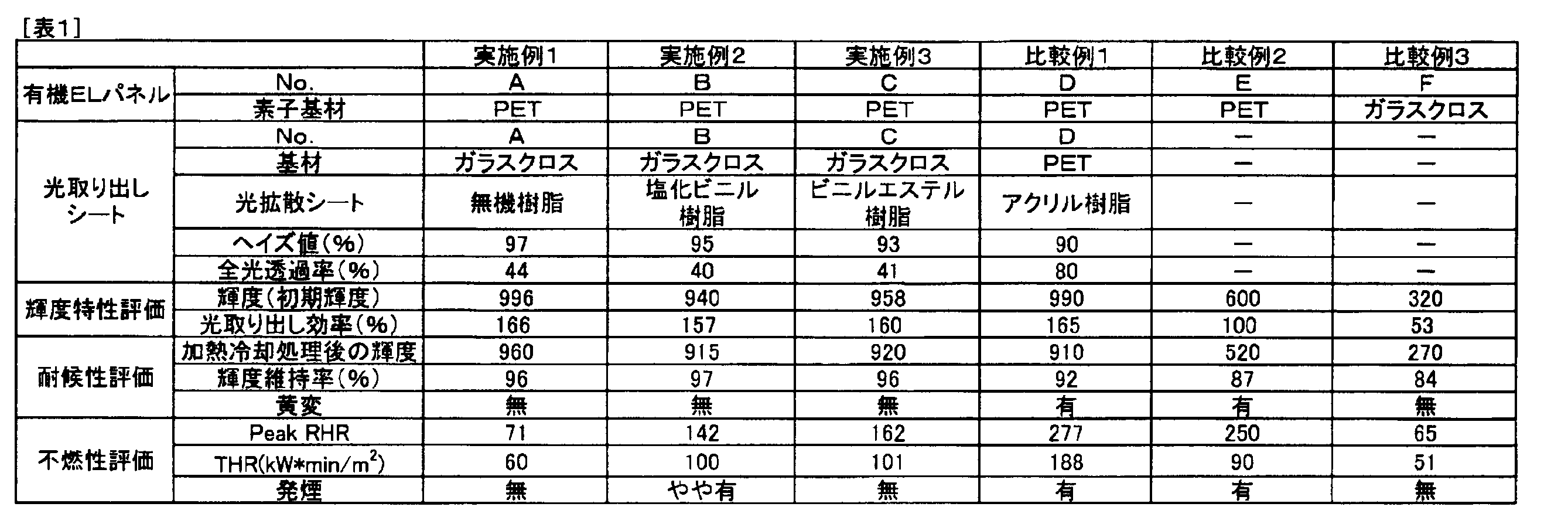
- a characteristic evaluation test was performed on the produced light extraction sheets A to D and organic EL panels A to F. Specifically, the light extraction sheets A to D were evaluated for their haze value and total light transmittance. In addition, the organic panels A to F were evaluated for luminance characteristics, weather resistance, and nonflammability.
- the luminance characteristics were evaluated as follows. First, a direct current of 2.5 mA / cm 2 was passed between the anode and the cathode and the luminance (initial luminance) was measured on the organic EL panels A to F immediately after fabrication. The luminance was measured using a spectral radiance meter (CS-2000 manufactured by Konica Minolta Optics).
- the luminance characteristics of the organic EL panels A to D having the light extraction sheets A to D and the organic EL panels A to D of the comparative example 1 with respect to the luminance of the organic EL panel E of the comparative example 2 having no light extraction sheet are extracted. Evaluated as efficiency. That is, the value obtained by dividing the luminance of the organic EL panels A to D by the luminance of the organic EL panel E was defined as the light extraction efficiency. The larger the light extraction efficiency, the better the result.
- ⁇ Weather resistance evaluation> Each of the organic EL panels A to F was placed in a cycle thermo, treated at 60 ° C. for 500 hours, naturally cooled, and then treated at ⁇ 20 ° C. for 500 hours.
- the luminance was measured in the same manner as the method described in ⁇ Luminance characteristic evaluation> above. Further, the organic EL panels A to F after the heating and cooling treatment were visually observed for yellowing.
- Table 1 shows the evaluation results.
- the light extraction efficiency of the organic EL panels A to C (Examples 1 to 3) including the light extraction sheet was good.
- the light extraction efficiency of the organic EL panels E and F (Comparative Examples 2 and 3) not including the light extraction sheet was not good.
- the light extraction efficiency is improved by providing the light extraction sheet.
- the luminance of the organic EL panel F (Comparative Example 3) using glass cloth as the element substrate was not particularly good as compared with the luminance of the organic EL panels A to E. This result is considered to be because the surface smoothness of the glass cloth is not as good as that of the PET film. Therefore, it was found that the effect of the present invention is exhibited when the organic EL element simply includes a glass cloth, and the light extraction sheet includes the glass cloth.
- the luminance maintenance rate after the heating and cooling process for the organic EL panels A to C of Examples 1 to 3 is the luminance maintenance of the organic EL panel D of Comparative Example 1 and the organic EL panels E and F of Comparative Examples 2 and 3. It was good compared with the rate. Specifically, the luminance maintenance ratio of the organic EL panels A to C was as high as 96% to 97%. In other words, it was found that there was almost no change in luminance even when the heating and cooling treatment was performed. However, in the organic EL panel D, the luminance maintenance rate was relatively low. In addition, in the organic EL panels E and F, the luminance maintenance rate was 90% or less, which was not good.
- Peak RHR maximum heat generation amount
- THR total heat generation amount for 2 minutes
- an organic EL element having both good light extraction efficiency and excellent weather resistance can be provided. Specifically, it has been found that it is possible to provide an organic EL device that exhibits good initial luminance and light extraction efficiency, and has excellent luminance resistance and excellent weather resistance such as no yellowing. Moreover, according to the organic EL panel of this invention, it turned out that it is excellent also in nonflammability.
- the organic EL element of the present invention when applied to various uses such as a display and a lighting device, a new function can be added in each use.
- Organic EL element body 1 Organic EL element body 2 Light extraction sheet (sheet) 3 Sealing material 4 Adhesive layer 10 Organic EL element
Landscapes
- Physics & Mathematics (AREA)
- Optics & Photonics (AREA)
- Electroluminescent Light Sources (AREA)
Description
前記陽極及び前記陰極のうちの少なくとも一方の電極であって、前記有機化合物層から放出された光が透過する電極の外側に設けられ、ガラスクロスを含んでなる光取り出し部材とを備えている
ことを特徴とする、有機エレクトロルミネッセンス素子。
ことを特徴とする、前記1に記載の有機エレクトロルミネッセンス素子。
本実施形態の有機EL素子は、陽極及び陰極からなる電極と、前記陽極及び前記陰極間に配置され、前記電極間に電圧が印加されることにより発光する有機化合物層とを備える有機エレクトロルミネッセンス素子本体部と、前記陽極及び前記陰極のうちの少なくとも一方の電極であって、前記有機化合物層から放出された光が透過する電極の外側に設けられ、ガラスクロスを含んでなる光取り出し部材とを備えている。そこで、本実施形態の有機EL素子を、図1を参照しながら説明する。なお、図1は、本実施形態の有機EL素子の一例であり、本発明の要旨を逸脱しない範囲内で、任意に変更して実施可能である。
有機EL素子10に備えられるガラスクロスシート2(光取り出し部材、以下、単に「シート2」と言う)は、詳細は後記する有機化合物層13から放出された光が透過する電極(図1に示す有機EL素子10では陽極12)の外側に設けられ、ガラスクロスを含んでなるものである。ただし、光取り出し部材の形状はシート状に何ら限定されず、例えば平板状等であってもよい。シート2は、通常は、ガラスクロスからなるガラスクロス基材2aと、有機EL素子本体部1が設けられる面とは反体側の面に形成される光拡散シート2bとが接着されて形成されてなる。
ガラスクロス基材2aは、ガラスクロスからなる。ガラスクロスは、ガラス繊維が織り込まれて(織成されて)形成されているものである。このようなガラスクロスの具体的な構成や種類、添加剤等は何ら限定されず、任意のガラスクロスが適用可能である。ただし、ガラスクロスは、通常は無色のものが好適である。また、ガラスクロス基材2aに適用可能なガラスクロスは、市販されているものであってもよく、適宜調製されたものであってもよい。また、ガラスクロスは、1種が単独で用いられてもよく、2種以上が任意に組み合わされて用いられてもよい。
ガラス繊維が長繊維の場合には、例えば、ガラス繊維を適宜引き揃えて固めたものが使用可能である。ただし、この場合、ガラス繊維は、撚りがかけられていることが好ましい。撚り数は特に制限されないが、例えば、100cmあたり、20回以上200回以下のものを使用することができる。撚り方向としては、右撚り(S撚り)、左撚り(Z撚り)のいずれであってもよい。また、撚り糸の形態としては、例えば、片撚り糸、諸撚り糸、ビッコ諸撚り糸、強ねん糸、壁撚り糸、駒撚り糸が挙げられる。
また、ガラス繊維が短繊維の場合には、例えば、ガラス繊維に対して撚りをかけて、つなぎ合わせた糸、即ち紡績糸が使用可能である。撚りの程度としては、長繊維の場合と同様の事項が適用可能である。
シート2を構成する光拡散シート2bは、ガラスクロス基材2aの表面に設けられるものである。光拡散シート2bは、ガラスクロス基材2aの片面のみに設けられていてもよく、両面に設けられていてもよい。また、光拡散シート2bは省略することもできる。さらに、例えばガラスクロスに対して光拡散シートを構成する成分を含浸させて、ガラスクロス基材2aと光拡散シート2bとが一体的に形成されてもよい。
シート2の物性は、特に制限されない。ただし、シート2のヘイズ値が90%以上であることが好ましく、93%以上がより好ましく、95%以上であることがよりさらに好ましく、97%以上が特に好ましい。ヘイズ値をこの範囲に設定することにより、より良好な光取り出し効率を図ることができる。
ヘイズ値(%)={拡散透過率(%)/全光透過率(%)}×100 ・・・(1)
また、ヘイズ値は、JIS-K-7136「プラスチック-透明材料のヘイズの求め方」、又は、ISO14782「Plastics-Determination of haze for transparent materials」に記載されている手法で測定することができる。
前記したように、本実施形態の有機EL素子10は、ガラスクロスを含むシート2を備えている。また、本実施形態の有機EL素子10は、シート2以外にも、図1に示す有機EL素子本体部1、封止材3及び接着層4を備えている。ただし、封止材3及び接着層4は、適宜設けないようにしてもよい。
有機EL素子本体部1は、陽極12及び陰極14からなる電極と、陽極12及び陰極14間に配置され、電極(陽極12及び陰極14)間に電圧が印加されることにより発光する有機化合物層13とを備えるものである。有機EL素子10から取り出される光は、通常、有機EL素子本体部1から放出された光である。
(1)発光層/電子輸送層
(2)正孔輸送層/発光層/電子輸送層
(3)正孔輸送層/発光層/正孔阻止層/電子輸送層
(4)正孔輸送層/発光層/正孔阻止層/電子輸送層/電子注入層(陰極バッファー層)
(5)正孔注入層(陽極バッファー層)/正孔輸送層/発光層/正孔阻止層/電子輸送層/電子注入層
(6)正孔注入層/正孔輸送層/発光層/電子輸送層/電子注入層
素子基板11(基体、基板、基材、支持体等)は、例えば、ガラス、プラスチック等の透明性材料で形成することができる。ただし、素子基板11は、薄膜ガラス、透明樹脂フィルム等の可撓性のある基材で構成されることが好ましい。また、素子基板11は、透明樹脂材料により構成されることが好ましい。従って、素子基板11は、透明樹脂フィルムにより構成されることが好ましい。
素子基板11と有機化合物層12との間には、防湿の観点から、1層又は2層以上のガスバリア層が形成されることが好ましい。なお、図1においては、ガスバリア層は図示していない。
陽極12は、有機化合物層1(具体的には発光層)に正孔を供給(注入)する電極膜である。陽極12の種類や物性は特に制限されず、任意に設定できる。例えば、陽極12は、仕事関数の大きい(4eV以上)、例えば、金属、合金、電気伝導性化合物、及び、これらの混合物等の電極材料で形成可能である。また、陽極12は、酸化インジウム錫や酸化インジウム亜鉛等の光透過性を有する材料(透明電極)により構成されてもよい。
有機化合物層13は、通常は、発光層に加えて、キャリア(正孔及び電子)の注入層、阻止層及び輸送層等の各種有機層を備える。以下、各有機層の構成を説明するが、これらの有機層は図1においては図示していない。また、各種有機層の具体的な材料等は公知の材料等を適用可能であるため、その説明を省略する。
発光層は、陽極12から直接、又は、陽極12から正孔輸送層等を介して注入される正孔と、陰極14から直接、又は、陰極14から電子輸送層等を介して注入される電子とが再結合することにより、発光する層である。なお、発光する部分は、発光層の内部であってもよいし、発光層とそれに隣接する層との間の界面であってもよい。
注入層は、駆動電圧の低下や発光輝度の向上を図るための層である。注入層は、通常は、電極及び発光層の間に設けられる。注入層は、通常は2つに大別される。即ち、注入層は、正孔(キャリア)を注入する正孔注入層、及び、電子(キャリア)を注入する電子注入層に大別される。正孔注入層(陽極バッファー層)は、陽極12と、発光層又は正孔輸送層との間に設けられる。また、電子注入層(陰極バッファー層)は、陰極14と、発光層又は電子輸送層との間に設けられる。
阻止層は、キャリア(正孔、電子)の輸送が阻止されるための層である。阻止層は、通常は2つに大別される。即ち、阻止層は、正孔(キャリア)の輸送が阻止される正孔阻止層、及び、電子(キャリア)の輸送が阻止される電子阻止層に大別される。
輸送層は、キャリア(正孔及び電子)を輸送する層である。輸送層は、通常は2つに大別される。即ち、輸送層は、正孔(キャリア)を輸送する正孔輸送層、及び、電子(キャリア)を輸送する電子輸送層に大別される。
陰極14は、発光層に電子を供給(注入)する電極膜である。陰極14を構成する材料は特に制限されないが、通常、仕事関数の小さい(4eV以下)、例えば、金属(電子注入性金属)、合金、電気伝導性化合物、及び、これらの混合物等の電極材料で形成される。
封止材3は、外気から有機EL素子本体部1等を保護するものである。封止材3の具体的な構成は特に制限されない。ただし、封止材3として可撓性材料を使用する場合には、封止材3は、樹脂層とガスバリア層とが積層されてなることが好ましい。
接着層4は、有機EL素子本体部1、シート2及び封止材3を接着固定する層である。即ち、シート2(光取り出し部材)は、陽極12に対して、接着層4によって接着されて設けられていることになる。ただし、シート2が陰極14の外側に設けられている場合には、シート2(光取り出し部材)は、陰極14に対して、接着層4によって接着されて設けられていることになる。接着層4は、通常は、接着剤を塗布して固化することにより形成される。
次に、本実施形態の有機EL素子の製造方法を説明する。ただし、以下に説明する方法は、本実施形態の有機EL素子を製造可能な方法の一例であり、本実施形態の有機EL素子の製造方法は以下の内容に何ら限定されるものではない。
本処理において、ガラスクロスはヒートクリーニングされる。具体的には、ガラスクロスが加熱される。この処理により、ガラスクロスの生機に付着した集束剤等を除去することができる。ヒートクリーニング処理の条件は特に制限されないが、例えば300℃~400℃程度の加熱炉を用い、ヒートクリーニング処理が可能である。また、処理時間も特に制限はされないが、通常は24時間以上、好ましくは48時間以上、また、通常は120時間以下、好ましくは96時間以下とする。
本処理において、ヒートクリーニング処理されたガラスクロスに対して、シランカップリング剤によって処理が行われる。この処理により、ガラスクロスの表面改質が行われ、接着槽4等との接着性を向上させることができる。シランカップリング剤処理の条件は特に制限されないが、通常は、シランカップリング剤が溶解した溶液(シランカップリング剤溶液)を用いてガラスクロスの処理が行われる。これにより、ガラスクロス表面にシランカップリング剤が固着又は固定化される。
本処理においては、シランカップリング剤処理されたガラスクロスが、バインダを含むバインダ溶液に含浸される。これにより、ガラスクロスとバインダとが一体化したガラスクロスが作製される。含浸処理において使用可能なバインダは、特に制限はないが、例えば酢酸ビニル系樹脂、塩化ビニル系樹脂、アクリル系樹脂、ビニルエステル系樹脂、コロイダルシリカ等の無機系樹脂等が挙げられる。これらは1種が単独で用いられてもよく、2種以上が任意の比率及び組み合わせで用いられてもよい。
本処理においては、バインダ溶液が含浸されたガラスクロスが乾燥される。乾燥上限は特に制限されず、例えば25℃24時間程度乾燥処理を行うことができる。そして、このようにして作製されたガラスクロスは、本実施形態の有機EL素子に好適である。
<実施例1>
はじめに、プラズマCVD法による成膜を行うCVD装置を用いて、素子基板表面にガスバリア層として窒化珪素膜を含む、ガスバリア層付き素子基板を作製した。
固形分濃度が30質量部となり、25℃における粘度が250mPa・sとなり、pHが11(25℃)となり、比重が1.3(25℃)となるように、水に、コロイダルシリカ、シクロデキストリン、キトサン、プルラン及び酵素(シクロデキストリングルコシルトランスフェラーゼ、キトサナーザ、プルラナーゼ及びアミラーゼからなる混合物)を添加して混合することにより、バインダ溶液を得た。そして、このバインダ溶液をガラスクロス(ユニチカグラスファイバー社製 H201)に含浸させ、次いで含浸物を120℃2分間の乾燥条件で乾燥させることにより、光取り出しシートAを作製した。
光取り出しシートAに代えて、以下の方法により作製した光取り出しシートBを用いたこと以外は実施例1と同様にして、有機ELパネルBを作製した。
塩化ビニルと酢酸ビニルとの共重合体を主成分とする塩化ビニル樹脂(カネカ社製 カネビラック)100質量部に、可塑剤としてジブチルフタレートを15質量部添加し、メチルエチルケトン75質量部で希釈した溶液を調製した。この溶液をヒートクリーニングされたガラスクロス(ユニチカグラスファイバー社製 H201)に含浸させ、120℃で乾燥させることにより、溶液中のメチルエチルケトンを揮発させた。これにより、樹脂組成物を含浸させたガラスクロスを得た。
光取り出しシートAに代えて、以下の方法により作製した光取り出しシートCを用いたこと以外は実施例1と同様にして、有機ELパネルCを作製した。
ビニルエステル樹脂(昭和高分子社製 SSP50-C06)100質量部と、パーカドックスP16(化薬アクゾ社製)0.5質量部と、パーキュアHO(日本樹脂社製)0.5質量部との混合物に対して、スターラを用いて約20分撹拌した。そして、攪拌後の混合物を約30分真空下に放置して脱気し、未硬化の樹脂組成物を得た。
光取り出しシートAに代えて、以下の方法により作製した光取り出しシートD(ガラスクロスを含まない)を用いたこと以外は実施例1と同様にして、有機ELパネルDを作製した。
アクリルポリオール(アクリディック49-394IM<固形分60%>、三井武田ケミカル社)32質量部と、シリカ樹脂粒子(平均粒径27.2μm)180質量部と、シリコン樹脂粒子(平均粒径30.0μm)40質量部と、酢酸ブチル215質量部との組成で調製された光取り出しシート用溶液を、厚さ100μmのPETフィルムに塗布して乾燥させることにより、光取り出しシートDを作製した。
光取り出しシートAを貼着しなかったこと以外は実施例1と同様にして、有機ELパネルEを作製した。
光取り出しシートAを貼着せず、さらに、有機EL素子本体部を構成する素子基板としてPETフィルムに代えてガラスクロスを用いたこと以外は実施例1と同様にして、有機ELパネルFを作製した。比較例3において、有機EL素子本体部の素子基板は以下のようにして作製した。
作製した光取り出しシートA~D及び有機ELパネルA~Fについて、特性評価試験を行った。具体的には、光取り出しシートA~Dについては、そのヘイズ値及び全光透過率についての評価を行った。また、有機パネルA~Fについては、輝度特性、耐候性及び不燃性についての評価を行った。
作製した光取り出しシートA~Dについて、前記の[1.有機EL素子の構造]に記載の方法に従って、ヘイズ値及び全光透過率を測定した。
輝度特性は以下のようにして評価した。まず、作製直後の有機ELパネルA~Fに対して、陽極及び陰極間に2.5mA/cm2の直流電流を流し、輝度(初期輝度)を測定した。輝度は、分光放射輝度計(コニカミノルタオプティクス社製 CS-2000)を用いて測定した。
有機ELパネルA~Fの各有機ELパネルをサイクルサーモに入れ、60℃で500時間処理した後自然冷却し、その後、-20℃で500時間処理した。これらの加熱冷却処理後の有機ELパネルA~Fについて輝度を測定し、作製直後の輝度(初期輝度)に対する輝度の維持率(=(処理後の輝度)/(初期輝度))として評価した。なお、輝度は、前記の<輝度特性評価>において記載した方法と同様にして測定した。また、加熱冷却処理後の有機ELパネルA~Fについて、黄変の有無を目視により観察した。
有機ELパネルA~Fの各有機ELパネルに輻射熱で3.5W/cm2の熱を加えた状態で、さらに、有機ELパネルA~Fの各有機ELパネルに対して炎を5分間当てた。その際の最大発熱量Peak RHR(Rated Heat Release)、及び、2分間の総発熱量THR(Total Heat Release)を測定した。さらに、その際の発煙の有無について評価した。なお、最大発熱量及び総発熱量は、いずれも小さい方が良好な結果を示している。
評価結果を表1に示す。
2 光取り出しシート(シート)
3 封止材
4 接着層
10 有機EL素子
Claims (2)
- 陽極及び陰極からなる電極と、前記陽極及び前記陰極間に配置され、前記電極間に電圧が印加されることにより発光する有機化合物層とを備える有機エレクトロルミネッセンス素子本体部と、
前記陽極及び前記陰極のうちの少なくとも一方の電極であって、前記有機化合物層から放出された光が透過する電極の外側に設けられ、ガラスクロスを含んでなる光取り出し部材とを備えている
ことを特徴とする、有機エレクトロルミネッセンス素子。 - 前記光取り出し部材は、前記陽極及び前記陰極のうちの少なくとも一方の側に対して、接着層によって接着されて設けられている
ことを特徴とする、請求項1に記載の有機エレクトロルミネッセンス素子。
Priority Applications (2)
| Application Number | Priority Date | Filing Date | Title |
|---|---|---|---|
| US14/413,920 US20150162566A1 (en) | 2012-07-27 | 2013-06-26 | Organic electroluminescent element |
| JP2014526827A JP6287837B2 (ja) | 2012-07-27 | 2013-06-26 | 有機エレクトロルミネッセンス素子 |
Applications Claiming Priority (2)
| Application Number | Priority Date | Filing Date | Title |
|---|---|---|---|
| JP2012166511 | 2012-07-27 | ||
| JP2012-166511 | 2012-07-27 |
Publications (1)
| Publication Number | Publication Date |
|---|---|
| WO2014017242A1 true WO2014017242A1 (ja) | 2014-01-30 |
Family
ID=49997059
Family Applications (1)
| Application Number | Title | Priority Date | Filing Date |
|---|---|---|---|
| PCT/JP2013/067495 Ceased WO2014017242A1 (ja) | 2012-07-27 | 2013-06-26 | 有機エレクトロルミネッセンス素子 |
Country Status (3)
| Country | Link |
|---|---|
| US (1) | US20150162566A1 (ja) |
| JP (1) | JP6287837B2 (ja) |
| WO (1) | WO2014017242A1 (ja) |
Cited By (1)
| Publication number | Priority date | Publication date | Assignee | Title |
|---|---|---|---|---|
| JP2015159066A (ja) * | 2014-02-25 | 2015-09-03 | コニカミノルタ株式会社 | 有機エレクトロルミネッセンス用光拡散シート及び有機エレクトロルミネッセンスパネル |
Families Citing this family (3)
| Publication number | Priority date | Publication date | Assignee | Title |
|---|---|---|---|---|
| US9978812B2 (en) * | 2014-01-14 | 2018-05-22 | Sharp Kabushiki Kaisha | Organic electroluminescent display panel |
| TW202541675A (zh) * | 2018-12-28 | 2025-10-16 | 日商半導體能源研究所股份有限公司 | 發光裝置、照明裝置、顯示裝置、模組及電子機器 |
| USD913326S1 (en) * | 2019-11-12 | 2021-03-16 | Thales Avs France Sas | Display screen or portion thereof with animated graphical user interface |
Citations (5)
| Publication number | Priority date | Publication date | Assignee | Title |
|---|---|---|---|---|
| JP2003109747A (ja) * | 2001-07-24 | 2003-04-11 | Matsushita Electric Works Ltd | 有機エレクトロルミネッセンス面発光体及び液晶表示装置 |
| JP2005326492A (ja) * | 2004-05-12 | 2005-11-24 | Sumitomo Bakelite Co Ltd | 光拡散シートおよび液晶ディスプレイ用バックライト |
| JP2006040864A (ja) * | 2004-01-14 | 2006-02-09 | Sumitomo Bakelite Co Ltd | 直下型バックライト用拡散板およびバックライトシステム |
| JP2006039503A (ja) * | 2004-01-14 | 2006-02-09 | Sumitomo Bakelite Co Ltd | 光拡散シートおよび液晶ディスプレイ用バックライト |
| JP2010137582A (ja) * | 2010-03-24 | 2010-06-24 | Nitto Boseki Co Ltd | ガラス繊維シート |
Family Cites Families (36)
| Publication number | Priority date | Publication date | Assignee | Title |
|---|---|---|---|---|
| JP2762993B2 (ja) * | 1996-11-19 | 1998-06-11 | 日本電気株式会社 | 発光装置及びその製造方法 |
| US6180304B1 (en) * | 1998-09-17 | 2001-01-30 | Eastman Kodak Company | Translucent imaging paper display materials with biaxially oriented polyolefin sheet |
| JP3669299B2 (ja) * | 2001-07-12 | 2005-07-06 | 住友化学株式会社 | メタクリル酸メチル系樹脂組成物およびその成形体 |
| JP2002221609A (ja) * | 2001-10-05 | 2002-08-09 | Central Glass Co Ltd | 耐熱性光拡散シート |
| US6963451B2 (en) * | 2001-11-22 | 2005-11-08 | Takiron Co., Ltd. | Light diffusive sheet |
| KR100730320B1 (ko) * | 2002-05-28 | 2007-06-19 | 마츠시다 덴코 가부시키가이샤 | 광회로-전기회로 혼재기판용 재료 및 광회로-전기회로혼재기판 |
| US6787994B2 (en) * | 2002-09-04 | 2004-09-07 | Eastman Kodak Company | OLED area illumination light source having a plurality of segments |
| JP4082680B2 (ja) * | 2003-07-02 | 2008-04-30 | ヤマウチ株式会社 | 樹脂ロールの製造方法 |
| JP2005140980A (ja) * | 2003-11-06 | 2005-06-02 | Nitto Denko Corp | 積層フィルム |
| CN101514080B (zh) * | 2004-05-13 | 2011-02-02 | 旭玻璃纤维股份有限公司 | 聚碳酸酯树脂强化用玻璃纤维以及聚碳酸酯树脂成形品 |
| JPWO2006088151A1 (ja) * | 2005-02-18 | 2008-07-03 | 富士フイルム株式会社 | 光拡散光学部材 |
| TWI434073B (zh) * | 2006-01-06 | 2014-04-11 | Sumitomo Chemical Co | 多層光擴散板 |
| JP4832094B2 (ja) * | 2006-02-01 | 2011-12-07 | 大日精化工業株式会社 | 光学用光拡散フィルム |
| US20070236938A1 (en) * | 2006-03-31 | 2007-10-11 | 3M Innovative Properties Company | Structured Composite Optical Films |
| SK51202007A3 (sk) * | 2006-10-24 | 2008-08-05 | Sumitomo Chemical Company, Limited | Prostriedok živice rozptyľujúcej svetlo |
| CN102051141B (zh) * | 2007-01-10 | 2014-12-17 | 日立化成株式会社 | 电路部件连接用粘接剂及使用该粘接剂的半导体装置 |
| US20110141402A1 (en) * | 2008-07-08 | 2011-06-16 | Sharp Kabushiki Kaisha | Lighting device, display device and television receiver |
| KR101925772B1 (ko) * | 2008-07-10 | 2018-12-06 | 가부시키가이샤 한도오따이 에네루기 켄큐쇼 | 발광 장치 및 전자 기기 |
| JP5381992B2 (ja) * | 2008-09-22 | 2014-01-08 | コニカミノルタ株式会社 | 面発光パネル |
| JP2011003522A (ja) * | 2008-10-16 | 2011-01-06 | Semiconductor Energy Lab Co Ltd | フレキシブル発光装置、電子機器及びフレキシブル発光装置の作製方法 |
| KR100964234B1 (ko) * | 2008-12-11 | 2010-06-17 | 삼성모바일디스플레이주식회사 | 유기 발광 디스플레이 장치 |
| US9834684B2 (en) * | 2009-03-11 | 2017-12-05 | Imerys Filtration Minerals, Inc. | Natural amorphous silica filler products |
| US8405116B2 (en) * | 2009-03-18 | 2013-03-26 | Semiconductor Energy Laboratory Co., Ltd. | Lighting device |
| EP2490506A1 (en) * | 2009-10-15 | 2012-08-22 | Asahi Glass Company, Limited | Organic led element, glass frit for diffusion layer for use in organic led element, and method for production of diffusion layer for use in organic led element |
| TWI408405B (zh) * | 2009-10-27 | 2013-09-11 | Eternal Chemical Co Ltd | 光學膜複合物 |
| US20110135907A1 (en) * | 2009-12-09 | 2011-06-09 | Kiarash Alavi Shooshtari | Fiber reinforced composite materials and methods for their manufacture and use |
| US20130090031A1 (en) * | 2010-04-06 | 2013-04-11 | Ferrania Technologies S.P.A. | Composite film material comprising a resin of fluorene crotonate, fluorene cinnamate, fluorene acrylate, fluorene methacrylate, fluorene allylether or a combination thereof |
| JP5638841B2 (ja) * | 2010-06-01 | 2014-12-10 | 株式会社ダイフレックス | コンクリート片及びタイルの剥落防止用一成分型ポリウレタン樹脂組成物及びこれを用いたコンクリート片及びタイルの剥落を防止する方法 |
| SG10201504246UA (en) * | 2010-06-02 | 2015-06-29 | Mitsubishi Gas Chemical Co | Resin composition, and prepreg and laminated sheet using the same |
| CN103221451B (zh) * | 2010-11-17 | 2015-11-25 | 日本化药株式会社 | 透明片材用环氧树脂组合物及其固化物 |
| CN103269851B (zh) * | 2010-12-27 | 2015-04-01 | 柯尼卡美能达株式会社 | 气体阻隔性膜及电子器件 |
| JP5225441B2 (ja) * | 2011-08-08 | 2013-07-03 | 日東電工株式会社 | 光拡散性不燃複合部材 |
| KR20140099527A (ko) * | 2011-12-01 | 2014-08-12 | 스미토모 베이클리트 컴퍼니 리미티드 | 화상 표시 장치 |
| KR101887217B1 (ko) * | 2012-01-06 | 2018-08-10 | 삼성디스플레이 주식회사 | 표시 장치 및 표시 장치의 제조 방법 |
| US9891353B2 (en) * | 2013-04-10 | 2018-02-13 | Nitto Denko Corporation | Light-diffusing-element manufacturing method and light-diffusing element |
| JP2015159066A (ja) * | 2014-02-25 | 2015-09-03 | コニカミノルタ株式会社 | 有機エレクトロルミネッセンス用光拡散シート及び有機エレクトロルミネッセンスパネル |
-
2013
- 2013-06-26 JP JP2014526827A patent/JP6287837B2/ja not_active Expired - Fee Related
- 2013-06-26 WO PCT/JP2013/067495 patent/WO2014017242A1/ja not_active Ceased
- 2013-06-26 US US14/413,920 patent/US20150162566A1/en not_active Abandoned
Patent Citations (5)
| Publication number | Priority date | Publication date | Assignee | Title |
|---|---|---|---|---|
| JP2003109747A (ja) * | 2001-07-24 | 2003-04-11 | Matsushita Electric Works Ltd | 有機エレクトロルミネッセンス面発光体及び液晶表示装置 |
| JP2006040864A (ja) * | 2004-01-14 | 2006-02-09 | Sumitomo Bakelite Co Ltd | 直下型バックライト用拡散板およびバックライトシステム |
| JP2006039503A (ja) * | 2004-01-14 | 2006-02-09 | Sumitomo Bakelite Co Ltd | 光拡散シートおよび液晶ディスプレイ用バックライト |
| JP2005326492A (ja) * | 2004-05-12 | 2005-11-24 | Sumitomo Bakelite Co Ltd | 光拡散シートおよび液晶ディスプレイ用バックライト |
| JP2010137582A (ja) * | 2010-03-24 | 2010-06-24 | Nitto Boseki Co Ltd | ガラス繊維シート |
Cited By (2)
| Publication number | Priority date | Publication date | Assignee | Title |
|---|---|---|---|---|
| JP2015159066A (ja) * | 2014-02-25 | 2015-09-03 | コニカミノルタ株式会社 | 有機エレクトロルミネッセンス用光拡散シート及び有機エレクトロルミネッセンスパネル |
| US10018753B2 (en) | 2014-02-25 | 2018-07-10 | Konica Minolta, Inc. | Light diffusion sheet for organic electroluminescent element and organic electroluminescent panel |
Also Published As
| Publication number | Publication date |
|---|---|
| US20150162566A1 (en) | 2015-06-11 |
| JP6287837B2 (ja) | 2018-03-07 |
| JPWO2014017242A1 (ja) | 2016-07-07 |
Similar Documents
| Publication | Publication Date | Title |
|---|---|---|
| JP5900720B1 (ja) | 量子ドット保護フィルム、それを用いた量子ドットフィルム及びバックライトユニット | |
| KR101760225B1 (ko) | 파장 변환 시트용 보호 필름, 파장 변환 시트 및 백라이트 유닛 | |
| JP5193208B2 (ja) | 発光デバイス | |
| CN109070539B (zh) | 阻隔膜层叠体及其制造方法、波长转换片、背光单元、以及电致发光单元 | |
| JP6287837B2 (ja) | 有機エレクトロルミネッセンス素子 | |
| KR20180121919A (ko) | 광학 부재, 그리고, 그 광학 부재를 사용한 백라이트 유닛 및 액정 표시 장치 | |
| JP6003892B2 (ja) | 面状発光体 | |
| JP2017138558A (ja) | 画像表示装置 | |
| KR20170037939A (ko) | 폴리에스테르 필름을 포함하는 유기 발광 다이오드 광원 및 상기 광원으로부터의 광 추출을 개선하는 방법 | |
| CN116194284A (zh) | 阻气膜和波长转换片 | |
| KR101485524B1 (ko) | 컬링 방지 lcd 백라이트용 반사 시트 | |
| JP2010055894A (ja) | 発光素子用封止フィルム | |
| JP6950429B2 (ja) | 蛍光体保護フィルム、波長変換シート及び発光ユニット | |
| WO2017221549A1 (ja) | 有機エレクトロルミネッセンス発光体、照明装置、および鉄道車両 | |
| JP6194889B2 (ja) | 有機エレクトロルミネッセンス素子及び有機エレクトロルミネッセンス素子用光取り出しシート | |
| JP2018098134A (ja) | 光透過型有機エレクトロルミネッセンスパネルおよび有機エレクトロルミネッセンス光源装置 | |
| JP6319087B2 (ja) | 有機エレクトロルミネッセンス素子及び有機エレクトロルミネッセンス素子用光取り出しシート | |
| JP6089834B2 (ja) | 有機エレクトロルミネッセンス素子 | |
| CN101814560A (zh) | 一种光电器件用光学介质、发光器件和太阳能电池 | |
| JP6262108B2 (ja) | 機能性フィルムの製造方法 | |
| WO2017104185A1 (ja) | 照明装置 | |
| JP2017127990A (ja) | 発光体保護フィルム、波長変換シート、バックライトユニット、エレクトロルミネッセンス発光ユニット | |
| JP6314835B2 (ja) | 有機エレクトロルミネッセンスパネルの製造方法及び製造装置 | |
| JP2014123492A (ja) | 有機エレクトロルミネッセンスパネルとその製造方法及び製造装置 |
Legal Events
| Date | Code | Title | Description |
|---|---|---|---|
| 121 | Ep: the epo has been informed by wipo that ep was designated in this application |
Ref document number: 13822665 Country of ref document: EP Kind code of ref document: A1 |
|
| WWE | Wipo information: entry into national phase |
Ref document number: 14413920 Country of ref document: US |
|
| ENP | Entry into the national phase |
Ref document number: 2014526827 Country of ref document: JP Kind code of ref document: A |
|
| NENP | Non-entry into the national phase |
Ref country code: DE |
|
| 122 | Ep: pct application non-entry in european phase |
Ref document number: 13822665 Country of ref document: EP Kind code of ref document: A1 |