WO2014017231A1 - 有機発光素子の製造装置及び製造方法 - Google Patents
有機発光素子の製造装置及び製造方法 Download PDFInfo
- Publication number
- WO2014017231A1 WO2014017231A1 PCT/JP2013/067024 JP2013067024W WO2014017231A1 WO 2014017231 A1 WO2014017231 A1 WO 2014017231A1 JP 2013067024 W JP2013067024 W JP 2013067024W WO 2014017231 A1 WO2014017231 A1 WO 2014017231A1
- Authority
- WO
- WIPO (PCT)
- Prior art keywords
- sheet
- roll
- substrate
- light emitting
- organic light
- Prior art date
- Legal status (The legal status is an assumption and is not a legal conclusion. Google has not performed a legal analysis and makes no representation as to the accuracy of the status listed.)
- Ceased
Links
Images



Classifications
-
- H—ELECTRICITY
- H05—ELECTRIC TECHNIQUES NOT OTHERWISE PROVIDED FOR
- H05B—ELECTRIC HEATING; ELECTRIC LIGHT SOURCES NOT OTHERWISE PROVIDED FOR; CIRCUIT ARRANGEMENTS FOR ELECTRIC LIGHT SOURCES, IN GENERAL
- H05B33/00—Electroluminescent light sources
- H05B33/10—Apparatus or processes specially adapted to the manufacture of electroluminescent light sources
-
- H—ELECTRICITY
- H10—SEMICONDUCTOR DEVICES; ELECTRIC SOLID-STATE DEVICES NOT OTHERWISE PROVIDED FOR
- H10K—ORGANIC ELECTRIC SOLID-STATE DEVICES
- H10K71/00—Manufacture or treatment specially adapted for the organic devices covered by this subclass
-
- H—ELECTRICITY
- H10—SEMICONDUCTOR DEVICES; ELECTRIC SOLID-STATE DEVICES NOT OTHERWISE PROVIDED FOR
- H10K—ORGANIC ELECTRIC SOLID-STATE DEVICES
- H10K71/00—Manufacture or treatment specially adapted for the organic devices covered by this subclass
- H10K71/10—Deposition of organic active material
- H10K71/12—Deposition of organic active material using liquid deposition, e.g. spin coating
- H10K71/13—Deposition of organic active material using liquid deposition, e.g. spin coating using printing techniques, e.g. ink-jet printing or screen printing
Definitions
- the present invention relates to an organic light emitting device manufacturing apparatus and manufacturing method.
- the manufacturing method of the organic LED is roughly divided into a vacuum deposition method and a coating method.
- the coating method has advantages such as easy formation of a large area and high material utilization efficiency.
- As a method of obtaining a white light source device by a coating method it is conceivable to form a laminated structure by repeatedly forming each organic layer by a printing method.
- Patent Document 1 So far, as a system for manufacturing an organic light-emitting element, a configuration of a manufacturing apparatus that repeats printing and drying has been studied, and reported in Patent Document 1.
- the conventional system for manufacturing an organic light emitting device has a problem that the apparatus becomes large.
- An object of the present invention is to make an organic light emitting device manufacturing apparatus compact.
- the features of the present invention for solving the above problems are as follows, for example.
- the sheet-shaped substrate has a plurality of print heads and a plurality of drying units, the sheet-like base material moves in a zigzag manner, and the organic layer constituting the organic light-emitting element is printed on the sheet-like base material by the plurality of print heads.
- the organic light emitting device manufacturing apparatus in which the organic substrate printed on the sheet substrate is dried by a plurality of drying units by moving the substrate in a zigzag manner.
- a method for producing an organic light emitting device having a sheet-like substrate and an organic layer wherein the sheet-like substrate moves in a zigzag manner, and an organic layer constituting the organic light emitting device is printed on the sheet-like substrate by a plurality of print heads Then, the sheet-like substrate is moved in a zigzag manner, and the organic layer printed on the sheet-like substrate is dried by a plurality of drying units.
- an organic light emitting device manufacturing apparatus with a reduced size can be applied. Problems, configurations, and effects other than those described above will be clarified by the following description of embodiments.
- Sectional drawing of the manufacturing apparatus of the organic light emitting element in one Embodiment of this invention The figure which looked at the manufacturing apparatus of the organic light emitting element in one Embodiment of this invention from the upper part. Sectional drawing of the manufacturing apparatus of the organic light emitting element in the one comparison form of this invention. Sectional drawing of the manufacturing apparatus of the organic light emitting element in one Embodiment of this invention. Sectional drawing of the manufacturing apparatus of the organic light emitting element in one Embodiment of this invention. The figure which looked at the manufacturing apparatus of the organic light emitting element in one Embodiment of this invention from the upper part.
- the print head drying section is arranged substantially linearly, whereas in the organic light emitting device manufacturing apparatus according to an embodiment of the present invention, the sheet-like substrate is spiral. Or it has a structure that moves in a zigzag manner.
- FIG. 1 is a cross-sectional view of an organic light emitting device manufacturing apparatus according to an embodiment of the present invention.
- the organic light emitting device manufacturing apparatus of FIG. 1 has a plurality of print heads and a plurality of drying units, and the sheet-like substrate moves spirally, and the plurality of print heads organically form the sheet-like substrate.
- An organic light-emitting device manufacturing apparatus in which an organic layer constituting a light-emitting element is printed, a sheet-like base material moves spirally, and the organic layer printed on the sheet-like base material is dried by a plurality of drying units. is there.
- the sheet-like substrate 1 is supplied from a roll 8, and the sheet-like substrate 1 on which an organic layer such as a hole injection layer is formed is wound by a winding roll 22.
- the sheet-like substrate 1 is an ultrathin glass substrate. However, it is not limited to a glass substrate, and a plastic substrate or a metal substrate provided with an appropriate water permeability lowering protective film can also be used.
- an electrode is formed on the sheet-like substrate 1.
- a glass substrate having a thickness of 50 ⁇ m was used for the sheet-like substrate 1.
- transparent electrode ITO was used as an electrode formed on the sheet-like base material 1.
- the feed rate of the sheet-like base material 1 was 5 m / min.
- the length of the organic light emitting device manufacturing apparatus in this example was 52 m.
- the sheet-like substrate 1 is supplied from the roll 8
- the sheet-like substrate 1 is conveyed from the roll 9 to the roll 10.
- a hole injection layer is formed on the sheet-like substrate 1 by the first printing head 2.
- the first print head 2 is, for example, a print head for a hole injection layer.
- the first print head 2 is supplied with hole injection layer ink from an ink tank (not shown) by a pump, and the hole injection layer is applied to the sheet-like substrate 1.
- the first print head 2 is not limited to the hole injection layer. It can also be used for a hole transport layer or an electron transport layer.
- PEDOT poly (3,4-ethylenedioxythiophene)
- PSS polystyrene sulfonate
- the sheet-like substrate 1 is conveyed from the roll 10 to the roll 11.
- the hole injection layer on the sheet-like substrate 1 is dried by the first drying unit 5. Since the sheet-like substrate 1 moves in a spiral shape, the angle formed by the straight line connecting the roll 9 and the roll 10 and the straight line connecting the roll 10 and the roll 11 is substantially a right angle. The angle formed by the straight line connecting the roll 9 and the roll 10 and the straight line connecting the roll 10 and the roll 11 does not have to be a substantially right angle, and may be an angle at which the sheet-like substrate 1 moves spirally. It ’s fine.
- the first drying unit 5 is for drying the hole injection layer. The hole injection layer is dried by blowing radiant heat or warm air.
- the region where the first print head 2 is present and the region where the first drying unit 5 is present are separated. If the first drying unit 5 and the first print head 2 are in the same place, the combustible gas generated in the first print head 2 may be ignited by the heat generated in the first drying unit 5, or the first There is a possibility that uneven printing may occur due to the temperature rise of the print head 2. Therefore, as shown in FIG. 1, the first printing head 2 and the first drying unit 5 are separated from each other so that the first drying unit 5 comes to the upper part of the first printing head 2, and the influence of the heat of the first drying unit 5. The first print head 2 is difficult to receive.
- the sheet-like substrate 1 is conveyed from the roll 11 to the roll 13 through the roll 12. Since the sheet-like substrate 1 moves in a spiral shape, the angle between the straight line connecting the roll 11 and the roll 12 and the straight line connecting the roll 12 and the roll 13 is substantially a right angle.
- the angle formed by the straight line connecting the roll 11 and the roll 12 and the straight line connecting the roll 12 and the roll 13 does not have to be a substantially right angle, and may be an angle at which the sheet-like substrate 1 moves spirally. It ’s fine.
- the sheet-like substrate 1 conveyed from the roll 13 is conveyed to the roll 15 through the roll 14.
- the line connecting the roll 14 and the roll 15 is on the inner side of the straight line connecting the roll 9 and the roll 10, that is, on the side where the winding roll 22 is formed with respect to the straight line connecting the roll 9 and the roll 10.
- the hole transport layer is applied onto the sheet-like substrate 1 by the second print head 3.
- the second print head 3 exists on the side where the winding roll 22 is formed with respect to the straight line connecting the roll 9 and the roll 10.
- the second print head 3 is a print head for the hole transport layer.
- the second print head 3 is supplied with hole transport layer ink from a hole transport layer ink tank (not shown) by a pump, and the hole transport layer ink is applied to the sheet-like substrate 1.
- the second print head 3 is not limited to the hole transport layer. It can also be used for a light emitting layer or a blocking layer.
- a triphenylamine polymer solution was used for the hole transport layer ink.
- the hole transport layer was printed on the sheet-like substrate 1 using the second print head 3 and dried at 150 ° C. for 10 minutes.
- the sheet-like substrate 1 is conveyed from the roll 15 to the roll 16, and further conveyed from the roll 16 to the roll 18 through the roll 17.
- the hole transport layer on the sheet-like substrate 1 is dried by the second drying unit 6.
- the in FIG. 1 two second drying sections 6 are provided, and the two second drying sections 6 are configured by a straight line connecting the roll 10 and the roll 11 and a straight line connecting the roll 11 and the roll 12. Is provided inside. Although two second drying sections 6 are provided in FIG. When the 2nd drying part 6 is provided with two or more like FIG.
- the 2nd drying part 6 has a curved structure. Since the sheet-like substrate 1 moves in a spiral shape, an angle formed by a straight line connecting the roll 14 and the roll 15 and a straight line connecting the roll 15 and the roll 16, and a straight line connecting the roll 15 and the roll 16 The angle formed between the roll 16 and the straight line connecting the roll 17 is substantially a right angle. The angle formed by the straight line connecting the roll 14 and the roll 15 and the straight line connecting the roll 15 and the roll 16 and the angle formed by the straight line connecting the roll 15 and the roll 16 and the straight line connecting the roll 16 and the roll 17 are It is not necessary to have a substantially right angle, and it is sufficient that the angle is such that the sheet-like substrate 1 moves spirally.
- the second drying unit 6 is for drying the hole transport layer.
- the hole transport layer is dried by blowing radiant heat or warm air.
- the area where the second print head 3 is present and the area where the second drying unit 6 is present are separated.
- the second printing head 3 and the second drying unit 6 are separated from each other, and the second drying unit 6 is positioned above the second printing head 3, so that the second drying unit 6 affects the heat.
- the print head 3 is difficult to receive.
- the sheet-like substrate 1 conveyed from the roll 17 is conveyed to the roll 19 through the roll 18.
- the line connecting the roll 18 and the roll 19 exists inside the straight line connecting the roll 14 and the roll 15, that is, on the side where the winding roll 22 is formed with respect to the straight line connecting the roll 14 and the roll 15.
- the light emitting layer is applied on the sheet-like substrate 1 by the third printing head 4.
- the third print head 4 exists on the side where the winding roll 22 is formed with respect to the straight line connecting the roll 14 and the roll 15.
- the third print head 4 is a print head for the light emitting layer.
- the third print head 4 is supplied with ink from a light emitting layer ink tank (not shown) by a pump, and the ink is applied to the sheet-like substrate 1.
- the third print head 4 is not limited to the light emitting layer. It can also be used for an electron transport layer or a hole transport layer.
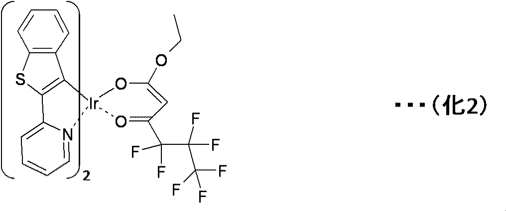
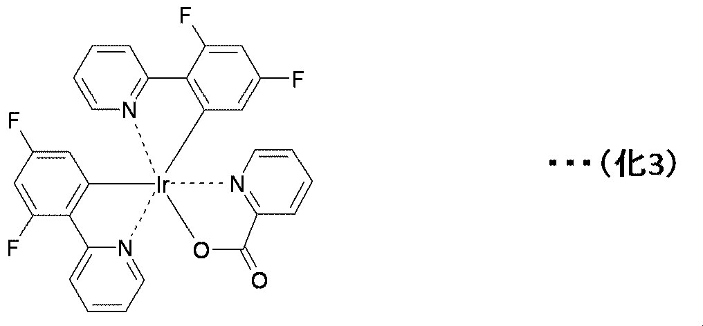
- the light emitting layer ink As the light emitting layer ink, a material represented by (Chemical Formula 1) for the host, a material represented by (Chemical Formula 2) for the red dopant, and a material represented by (Chemical Formula 3) for the blue dopant. A solution of a material represented by (Chemical Formula 4) was used as a green dopant. Using the 3rd printing head 4, the ink for light emitting layers was printed on the positive hole transport layer, and it dried at 120 degreeC for 10 minutes.
- the sheet-like substrate 1 is conveyed from the roll 19 to the roll 20, and further conveyed from the roll 20 through the roll 21 to the winding roll 22.
- the light emitting layer on the sheet-like substrate 1 is dried by the third drying unit 7.
- the two third drying sections 7 are provided, and the two third drying sections 7 are regions configured by a straight line connecting the roll 15 and the roll 16 and a straight line connecting the roll 16 and the roll 17. And is provided outside the region constituted by a straight line connecting the roll 19 and the roll 20 and a straight line connecting the roll 20 and the roll 21.
- the third drying section 7 has a bent structure. Since the sheet-like substrate 1 moves in a spiral shape, an angle formed by a straight line connecting the roll 19 and the roll 20 and a straight line connecting the roll 20 and the roll 21, and a straight line connecting the roll 20 and the roll 21 The angle formed by the straight line connecting the roll 21 and the roll 22 is substantially a right angle. An angle formed by a straight line connecting the roll 19 and the roll 20 and a straight line connecting the roll 20 and the roll 21, and an angle formed by a straight line connecting the roll 20 and the roll 21 and a straight line connecting the roll 21 and the winding roll 22. Need not be substantially right-angled, as long as the sheet-like substrate 1 moves at a spiral shape.
- the third drying unit 7 is for drying the light emitting layer.
- the luminescent layer is dried by blowing radiant heat or warm air.
- the area where the third print head 4 is present and the area where the third drying section 7 is present are separated.
- the third printing head 4 and the third drying unit 7 are separated from each other, and the third drying unit 7 is located above the third printing head 4, so that the third thermal unit 7 affects the heat.
- the print head 4 is difficult to receive.
- the sheet-like substrate 1 on which the organic layer is printed is wound by the winding roll 22.
- the organic light emitting device manufacturing apparatus has a structure in which the sheet-like substrate 1 moves in a spiral shape. By adopting such a structure, the footprint of the apparatus can be reduced and the size can be reduced.
- the sheet-like substrate 1 wound up by the winding roll 22 was moved to another apparatus, and an electron transport layer, an electron injection layer, and a cathode were formed by a vapor deposition method. Then, the sealing film was affixed and the organic light emitting element was formed. The voltage-current-luminance characteristics of the formed organic light emitting device were measured.
- FIG. 2 is a top view of the manufacturing apparatus of FIG.
- the first ink tank 23 supplies the hole injection layer ink to the sheet-like substrate 1.
- the second ink tank 24 supplies the hole transport layer ink to the sheet-like substrate 1.
- the third ink tank 25 supplies the light emitting layer ink to the sheet-like substrate 1.
- the first ink tank 23, the second ink tank 24, and the third ink tank 25 that supply ink to the print head are installed in a region different from the region in which the sheet-like substrate 1 moves. Yes. By doing so, the ink tank can be easily replaced and the workability is excellent.
- the hole injection layer is used for the purpose of improving luminous efficiency and lifetime. Moreover, although it is not essential, it is used for the purpose of relaxing the unevenness of the anode.
- the hole injection layer is preferably a conductive polymer such as PEDOT (poly (3,4-ethylenedioxythiophene)): PSS (polystyrene sulfonate).
- PEDOT poly (3,4-ethylenedioxythiophene)
- PSS polystyrene sulfonate
- a polypyrrole-based or triphenylamine-based polymer material can be used.
- phthalocyanine compounds and starburst amine compounds that are often used in combination with low molecular weight materials are also applicable.
- the electron transport layer is a layer that supplies electrons to the light emitting layer.
- an electron injection layer and a hole blocking layer are also included in the electron transport layer.
- the material for the electron transport layer include bis (2-methyl-8-quinolinolato) -4- (phenylphenolato) aluminum (hereinafter referred to as BAlq), tris (8-quinolinolato) aluminum (hereinafter referred to as Alq3), Tris, and the like.
- 3TPYMB (2,4,6-trimethyl-3- (pyridin-3-yl) phenyl) borane
- UGH2 1,4-Bis (triphenylsilyl) benzene
- UGH2 1,4-Bis (triphenylsilyl) benzene
- oxadiazole derivative triazole derivative
- Fullerene derivatives phenanthroline derivatives
- quinoline derivatives and the like
- the hole transport layer is made of a material having a function of transporting holes, and in a broad sense, a hole injection layer and an electron blocking layer are also included in the hole transport layer.
- a hole transport layer a starburst amine compound, a stilbene derivative, a hydrazone derivative, a thiophene derivative, or the like can be used. Further, the present invention is not limited to these materials, and two or more of these materials may be used in combination.
- the light emitting layer includes a host and a dopant. When white light is emitted from the light emitting layer, the dopant includes, for example, a red dopant, a green dopant, and a blue dopant.
- the material for forming the light emitting layer includes, for example, a host, a red dopant, a green dopant, and a blue dopant. However, if it becomes white light, the material for forming the light emitting layer includes a host, a red dopant and a blue dopant, a host, a red dopant and a green dopant, a host material, a blue dopant material and a green. It may be one containing a dopant. In this embodiment, the red dopant is present in the light emitting layer in the light emitting layer, and forms a pseudo laminated structure.
- each dopant is spontaneously phase-separated in the light emitting layer so that low energy dopants are not adjacent to each other, so that even in a coating type white light emitting element, highly efficient white light emission is possible. In this case, white light emission can be obtained even at a high dopant concentration.
- an appropriate functional group is added to each dopant below.
- the excitation energy of the host is sufficiently larger than the excitation energy of the blue dopant.
- the excitation energy is measured using an emission spectrum.
- Examples of the main skeleton of the red dopant material include rubrene, (E) -2- (2- (4- (dimethylamino) styryl) -6-methyl-4H-pyran-4-ylidene) malononitrile (DCM) and its derivatives.
- Iridium complexes such as Bis (1-phenylisoquinoline) (acetylacetonate) iridium (III)), osmium complexes, and europium complexes.
- the iridium complex represented by (Chemical Formula 5) is more preferable in terms of light emission characteristics, and more preferable is one having an acetylacetonate moiety.
- X1 represents an aromatic heterocycle containing N
- X2 represents an aromatic hydrocarbon ring or an aromatic heterocycle.
- Examples of the aromatic heterocycle represented by X1 include quinoline ring, isoquinoline ring, pyridine ring, quinoxaline ring, thiazole ring, pyrimidine ring, benzothiazole ring, oxazole ring, benzoxazole ring, indole ring and isoindole ring.
- Examples of the aromatic hydrocarbon ring or aromatic heterocycle represented by X2 include a benzene ring, naphthalene ring, anthracene ring, thiophene ring, benzothiophene ring, furan ring, benzofuran ring, and fluorene ring.
- a red dopant has the 1st functional group for moving to the surface side at the time of light emitting layer film forming. Thereby, the red dopant is unevenly distributed and localized on the surface side in the light emitting layer.
- the first functional group Y1 or Y2 added to the acetylacetonate site for transfer to the light emitting layer surface during film formation include a fluoroalkyl group, a perfluoroalkyl group, and an alkyl group (however, the number of C is 10). And the like), perfluoropolyether groups, and siloxy groups (—Si—O—Si—).
- the red dopant may have at least one of these functional groups, but may have a plurality of types.
- the main skeleton of the green dopant material examples include coumarin and derivatives thereof, and iridium complexes (Tris (2-phenylpyridine) iridium (III): hereinafter Ir (ppy) 3, etc.).
- the green dopant has a second functional group to be drawn to an electrode, a hole transport layer, or the like that is a base layer of the light emitting layer.
- the second functional group for attracting the underlying layer during film formation varies depending on the type of the underlying layer.
- the underlayer is a hole transport layer, examples thereof include a phenylamino group, an oxazole group, a carbazole group, and a hydrazone site that introduce a structure similar to that of the hole transport layer.
- the green dopant may have at least one of these functional groups, but may have a plurality of types.
- the underlayer is an electrode such as ITO or metal, for example, a hydroxy group (—OH), a thiol group (—SH), a carboxyl group (—COOH), a sulfo group (—SO 3 H), I, Br , Cl, F, SCN, CN , NH 2, NO 2, bipyridyl group.
- the green dopant may have at least one of these functional groups, but may have a plurality of types.
- Examples of the main skeleton of the blue dopant material include perylene and iridium complexes (Bis (3,5-difluoro-2- (2-pyridyl) phenyl- (2-carboxypyridyl) iridium (III)): FIrpic and the like).
- a functional group need not be added to the blue dopant, but a structure having a poor affinity with the underlayer may be introduced in order to more positively perform phase separation.
- An organic light emitting device was produced in the same manner as in Example 1 except that the manufacturing apparatus having the structure shown in FIG. FIG. 3 is a partial cross-sectional view of the manufacturing apparatus of Comparative Example 1.
- Example 1 In this apparatus, as in Example 1, three apparatuses of FIG. 3 were prepared in order to form the hole injection layer, the hole transport layer, and the light emitting layer by the printing method.
- the length of one device was 52 m, and the length of three devices was 158 m.
- the total length of the printing apparatus is about three times that in the first embodiment.
- the sheet-like base material 31 is supplied from the roll 34, and the sheet-like base material 31 on which an organic layer such as a hole injection layer is formed is wound by the winding roll 38.
- the sheet-like base material 31 is supplied from the roll 34, the sheet-like base material 31 is conveyed from the roll 35 to the roll 36.
- a hole injection layer is formed on the sheet-like base material 31 by the print head 32.
- the print head 32 is, for example, a print head for a hole injection layer.
- the print head 32 is supplied with hole injection layer ink by a pump from an ink tank (not shown), and the hole injection layer is applied to the sheet-like substrate 31.
- the sheet-like base material 31 is conveyed from the roll 36 to the roll 37.
- the hole injection layer on the sheet-like substrate 31 is dried by the drying unit 33.
- the drying unit 33 is for drying the hole injection layer.
- the hole injection layer is dried by blowing radiant heat or warm air.
- the sheet-like substrate 31 on which the hole injection layer is printed is wound by the winding roll 38. Thereafter, the wound sheet-like base material 31 is set on a roll 34, and a hole transport layer and a light emitting layer are formed on the sheet-like base material 31 in the same manner as the hole injection layer.
- the wound sheet-like substrate 1 was moved to another apparatus, and an electron transport layer, an electron injection layer, and a cathode were formed by an evaporation method. Then, the sealing film was affixed and the organic light emitting element was formed. The voltage-current-luminance characteristics of the formed element were measured. As a result, the driving voltage at a luminance of 1000 cd / m 2 was 1.2 times that of the organic light emitting device of Example 1. This is because, in this comparative example, each time the hole injection layer, the hole transport layer, and the light emitting layer are formed, it is wound up, so that the printed surface comes into contact with the back surface of the sheet-like substrate, and the printed surface is contaminated. It is thought that it was because of.
- FIG. 4 is a side view of the manufacturing apparatus according to the second embodiment.
- the manufacturing apparatus of Example 2 can print four layers of a hole injection layer, a hole transport layer, a light emitting layer, and an electron transport layer with one printing device.
- An organic light emitting device was produced in the same manner as in Example 1 except that this apparatus was used.
- the length of the apparatus of this example was 60 m.
- the sheet-like substrate 1 is conveyed to the roll 42 through the roll 41.
- the line connecting the roll 41 and the roll 42 exists inside the straight line connecting the roll 18 and the roll 19, that is, on the side where the winding roll 22 is formed with respect to the straight line connecting the roll 18 and the roll 19.
- the sheet-like base material 1 moves spirally.
- an electron transport layer is applied on the sheet-like substrate 1 by the fourth printing head 46.
- the fourth print head 46 is present on the side where the winding roll 22 is formed with respect to the straight line connecting the roll 18 and the roll 19.
- the fourth print head 46 is a print head for the electron transport layer.
- the fourth print head 46 is supplied with ink from an electron transport layer ink tank (not shown) by a pump to apply the ink to the sheet-like substrate 1.
- the sheet-like substrate 1 is conveyed from the roll 42 to the roll 43, conveyed from the roll 43 to the roll 44, and further wound from the roll 44 through the roll 45. It is conveyed to the roll 22.
- the fourth drying unit 47 causes the sheet-like substrate to be conveyed.
- the electron transport layer on the material 1 is dried.
- three fourth drying sections 47 are provided, and the three fourth drying sections 47 are regions configured by a straight line connecting the roll 19 and the roll 20 and a straight line connecting the roll 20 and the roll 21.
- the fourth drying section 47 has a bent structure. Since the sheet-like substrate 1 moves in a spiral shape, an angle formed by a straight line connecting the roll 42 and the roll 43 and a straight line connecting the roll 43 and the roll 44, and a straight line connecting the roll 43 and the roll 44, The angle formed by the roll 44 and the straight line connecting the rolls 45 is substantially a right angle.
- the fourth drying unit 47 is for drying the electron transport layer.
- the electron transport layer is dried by blowing radiant heat or warm air.
- the sheet-like substrate 1 on which the organic layer is printed is wound by the winding roll 22.
- the driving voltage at which the luminance was 1000 cd / m 2 was 0.8 times that of the organic light emitting device of Example 1.
- the surface of the light emitting layer does not come into contact with the back surface of the sheet-like substrate 1, so that the surface of the light emitting layer is not contaminated. Therefore, the driving voltage is considered to be lowered. .
- FIG. 5 shows a cross-sectional view of the production apparatus of Example 3.
- the manufacturing apparatus according to the third embodiment is characterized in that the sheet-like substrate 81 has a structure that moves in a zigzag manner.
- the apparatus for manufacturing an organic light-emitting element in the present embodiment has a plurality of print heads and a plurality of drying units, and the sheet-like substrate moves in a zigzag manner, and the plurality of print heads organically form the sheet-like substrate.
- An organic light-emitting device manufacturing apparatus in which an organic layer constituting a light-emitting element is printed, a sheet-like base material moves in a zigzag manner, and an organic layer printed on the sheet-like base material is dried by a plurality of drying units.
- the drying section blows air from above the drawing so that the sheet base material 81 moves in a zigzag shape.
- the length of this manufacturing apparatus is 40 m.
- An organic light emitting device was produced in the same manner as in Example 1 except that this apparatus was used. With the manufacturing apparatus as in the present embodiment, the apparatus can be made more compact than the manufacturing apparatus in the first embodiment.
- a sheet-like substrate 81 is supplied from a roll 88, and the sheet-like substrate 81 on which an organic layer such as a hole injection layer is formed is wound by a winding roll 101.
- the sheet-like base material 81 is supplied from the roll 88, the sheet-like base material 81 is conveyed from the roll 89 to the roll 90.
- a hole injection layer is formed on the sheet-like substrate 81 by the first print head 82.
- the first print head 82 is, for example, a print head for a hole injection layer.
- the first print head 82 is supplied with hole injection layer ink by a pump from an ink tank (not shown), and the hole injection layer is applied to the sheet-like substrate 81.
- the sheet-like substrate 81 is conveyed from the roll 91 through the roll 92 to the roll 93.
- the hole injection layer on the sheet-like substrate 81 is dried by the first drying unit 85.
- the sheet-like base material 81 moves in a zigzag manner in the first drying unit 85.
- the first drying unit 85 is for drying the hole injection layer.
- the hole injection layer is dried by blowing radiant heat or warm air.
- the sheet-like substrate 81 is conveyed from the roll 93 to the roll 95 through the roll 94.
- the hole transport layer is applied onto the sheet-like substrate 81 by the second print head 83.
- the second print head 83 is, for example, a print head for a hole transport layer.
- the second print head 83 is supplied with hole transport layer ink from a hole transport layer ink tank (not shown) by a pump, and the hole transport layer ink is applied to the sheet-like substrate 81.
- a first partition 805 is formed between the first drying unit 85 and the second drying unit 86.
- the sheet-like base material 81 moves in a zigzag manner within the first partition 805.
- the first partition 805 separates the first drying unit 85, the second drying unit 86, and the second print head 83 from each other.
- the heat generated in the first drying unit 85 or the second drying unit 86 is transmitted to the second print head 83, there is a possibility that the combustible gas generated in the second print head 83 may be ignited, or the second print head 83.
- the first partition 805 makes it difficult for heat generated in the first drying unit 85 and the second drying unit 86 to be transmitted to the second print head 83.
- the sheet-like substrate 81 is conveyed from the roll 95 to the roll 97 through the roll 96.
- the hole transport layer on the sheet-like substrate 81 is dried by the second drying unit 86.
- the sheet-like base material 81 moves in a zigzag manner in the second drying unit 86.
- the second drying unit 86 is for drying the hole transport layer.
- the hole transport layer is dried by blowing radiant heat or warm air.
- the sheet-like substrate 81 is conveyed from the roll 97 to the roll 99 through the roll 98.
- a light emitting layer is applied on the sheet-like substrate 81 by the third printing head 84.
- the third print head 84 is a light emitting layer print head.
- the third print head 84 is supplied with light emitting layer ink from a light emitting layer ink tank (not shown) by a pump, and the light emitting layer ink is applied to the sheet-like substrate 81.
- a second partition 806 is formed between the second drying unit 86 and the third drying unit 87.
- the sheet-like base material 81 is moved in a zigzag manner.
- the second partition 806 separates the second drying unit 86 and the third drying unit 87 from the third print head 84.
- the heat generated in the second drying unit 86 or the third drying unit 87 is transmitted to the third print head 84, there is a possibility that the flammable gas generated in the third print head 84 may be ignited, or the third print head 84.
- the second partition 806 makes it difficult for heat generated in the second drying unit 86 and the third drying unit 87 to be transmitted to the third print head 84.
- the sheet-like substrate 81 is conveyed from the roll 99 to the winding roll 101 through the roll 100.
- the light emitting layer on the sheet-like substrate 81 is dried by the third drying unit 87.
- the sheet-like base material 81 moves in a zigzag manner in the third drying unit 87.
- the third drying unit 87 is for drying the light emitting layer.
- the luminescent layer is dried by blowing radiant heat or warm air.
- the sheet-like substrate 81 on which the organic layer is printed is wound by the winding roll 101.
- the driving voltage at which the luminance was 1000 cd / m 2 was 1.0 times that of the organic light emitting device of Example 1.
- the figure which looked at the manufacturing apparatus of a present Example from the upper part in FIG. 6 was shown.
- the first ink tank 102 supplies the hole injection layer ink to the sheet-like substrate 81.
- the second ink tank 103 supplies the hole transport layer ink to the sheet-like substrate 81.
- the third ink tank 104 supplies the light emitting layer ink to the sheet-like substrate 81.
- the ink tank supplied to the print head is installed in a region different from the region in which the sheet-like substrate to be printed moves. For this reason, the ink tank can be easily replaced, and the workability is excellent.
Landscapes
- Engineering & Computer Science (AREA)
- Manufacturing & Machinery (AREA)
- Electroluminescent Light Sources (AREA)
Description
本発明は、有機発光素子の製造装置及び製造方法に関する。
有機LEDの製造方法は真空蒸着法と塗布法に大別される。そのうち、塗布法は大面積の成膜が容易、材料の利用効率が高いなどの利点がある。塗布法で白色の光源装置を得る方法としては、各有機層を繰り返し印刷法で形成し、積層構造を作製することが考えられる。
これまでに有機発光素子を製造するシステムとして、印刷と乾燥をくりかえす製造装置の構成が検討されており、特許文献1にて報告されている。
従来の有機発光素子を製造するシステムには、装置が大きくなるという問題があった。
本発明の目的は、有機発光素子の製造装置をコンパクトにすることである。
本発明の目的は、有機発光素子の製造装置をコンパクトにすることである。
上記課題を解決するための本発明の特徴は、例えば以下の通りである。
複数の印刷ヘッドと、複数の乾燥部と、を有し、シート状基材が渦巻状に移動して、複数の印刷ヘッドによりシート状基材に有機発光素子を構成する有機層が印刷され、シート状基材が渦巻状に移動して、複数の乾燥部によりシート状基材に印刷された有機層が乾燥される有機発光素子の製造装置。
複数の印刷ヘッドと、複数の乾燥部と、を有し、シート状基材が渦巻状に移動して、複数の印刷ヘッドによりシート状基材に有機発光素子を構成する有機層が印刷され、シート状基材が渦巻状に移動して、複数の乾燥部によりシート状基材に印刷された有機層が乾燥される有機発光素子の製造装置。
複数の印刷ヘッドと、複数の乾燥部と、を有し、シート状基材がジグザグに移動して、複数の印刷ヘッドによりシート状基材に有機発光素子を構成する有機層が印刷され、シート状基材がジグザグに移動して、複数の乾燥部によりシート状基材に印刷された有機層が乾燥される有機発光素子の製造装置。
シート状基材および有機層を有する有機発光素子の製造方法であって、シート状基材が渦巻状に移動して、複数の印刷ヘッドによりシート状基材に有機層が印刷され、シート状基材が渦巻状に移動して、複数の乾燥部によりシート状基材に印刷された有機層が乾燥される有機発光素子の製造方法。
シート状基材および有機層を有する有機発光素子の製造方法であって、シート状基材がジグザグに移動して、複数の印刷ヘッドによりシート状基材に有機発光素子を構成する有機層が印刷され、シート状基材がジグザグに移動して、複数の乾燥部によりシート状基材に印刷された有機層が乾燥される有機発光素子の製造方法。
本発明により、サイズが小さくなった有機発光素子の製造装置が適用できる。上記した以外の課題、構成及び効果は以下の実施形態の説明により明らかにされる。
以下、図面等を用いて、本発明の実施形態について説明する。以下の説明は本発明の内容の具体例を示すものであり、本発明がこれらの説明に限定されるものではなく、本明細書に開示される技術的思想の範囲内において当業者による様々な変更および修正が可能である。また、本発明を説明するための全図において、同一の機能を有するものは、同一の符号を付け、その繰り返しの説明は省略する場合がある。
従来の有機発光素子の製造装置では、印刷ヘッド乾燥部がほぼ直線的に配置されていたのに対して、本発明の一実施形態に係る有機発光素子の製造装置ではシート状基材が渦巻状またはジグザグに移動する構造となっている。
図1は本発明の一実施形態における有機発光素子の製造装置の断面図である。図1の有機発光素子の製造装置は、複数の印刷ヘッドと、複数の乾燥部と、を有し、シート状基材が渦巻状に移動して、複数の印刷ヘッドによりシート状基材に有機発光素子を構成する有機層が印刷され、シート状基材が渦巻状に移動して、複数の乾燥部によりシート状基材に印刷された前記有機層が乾燥される有機発光素子の製造装置である。
図1において、ロール8からシート状基材1が供給され、巻きロール22で正孔注入層などの有機層が形成されたシート状基材1が巻き取られる。シート状基材1は極薄型ガラス基材である。但し、ガラス基板に限るものではなく、適切な透水性低下保護膜を施したプラスティック基板や金属基板も用いることができる。本発明では図示していないが、シート状基材1には電極が形成されている。本実施例では、シート状基材1には厚さ50μmのガラス基板を用いた。シート状基材1に形成された電極には、透明電極のITOを用いた。シート状基材1の送り速度は5m/分とした。本実施例における有機発光素子の製造装置の長さは52mであった。
ロール8からシート状基材1が供給された後、シート状基材1はロール9からロール10に搬送される。シート状基材1がロール9からロール10に搬送される際、第一印刷ヘッド2によりシート状基材1上に正孔注入層が形成される。第一印刷ヘッド2は、例えば正孔注入層用の印刷ヘッドである。この第一印刷ヘッド2はインク用タンク(図示せず)からポンプにより正孔注入層インクが供給され、シート状基材1に正孔注入層が塗布される。第一印刷ヘッド2は正孔注入層用に限定されない。正孔輸送層用或いは電子輸送層用とすることも可能である。
本実施例では、正孔注入層用インクにPEDOT(ポリ(3、4-エチレンジオキシチオフェン)):PSS(ポリスチレンスルホネート)溶液を用いた。第一印刷ヘッド2を用いてシート状基材1上に正孔注入層を印刷し、200℃、10分で乾燥を行った。
シート状基材1に正孔注入層が塗布された後、シート状基材1はロール10からロール11に搬送される。シート状基材1がロール10からロール11に搬送される際、第一乾燥部5によりシート状基材1上の正孔注入層が乾燥される。シート状基材1が渦巻状に移動するために、ロール9とロール10を結んだ直線とロール10とロール11を結んだ直線とのなす角が略直角となっている。ロール9とロール10を結んだ直線とロール10とロール11を結んだ直線とのなす角は略直角である必要はなく、シート状基材1が渦巻状に移動するような角度となっていれば良い。第一乾燥部5は正孔注入層を乾燥させるためのものである。輻射熱或いは温風を吹き付けることにより正孔注入層を乾燥させる。
図1のように第一印刷ヘッド2が存在する領域と第一乾燥部5の存在する領域とが分離されている。第一乾燥部5と第一印刷ヘッド2が同じ場所にあると、第一乾燥部5で発生する熱により第一印刷ヘッド2で発生する可燃性ガスが引火する可能性があったり、第一印刷ヘッド2の温度上昇によって印刷むらが生じる可能性があったりする。そこで、図1のように第一印刷ヘッド2と第一乾燥部5とを離し、第一乾燥部5を第一印刷ヘッド2の上部に来るようにして、第一乾燥部5の熱の影響を第一印刷ヘッド2が受けにくい構造にしている。
シート状基材1上の正孔注入層が乾燥された後、シート状基材1はロール11からロール12を通ってロール13に搬送される。シート状基材1が渦巻状に移動するために、ロール11とロール12を結んだ直線とロール12とロール13を結んだ直線とのなす角が略直角となっている。ロール11とロール12を結んだ直線とロール12とロール13を結んだ直線とのなす角は略直角である必要はなく、シート状基材1が渦巻状に移動するような角度となっていれば良い。
ロール13から搬送されたシート状基材1は、ロール14を通ってロール15に搬送される。図1において、ロール14とロール15を結んだ線は、ロール9とロール10を結んだ直線の内側、つまり、ロール9とロール10を結んだ直線に対して巻きロール22が形成される側に存在する。シート状基材1がロール14を通ってロール15に搬送される際、第二印刷ヘッド3により、シート状基材1上に正孔輸送層が塗布される。第二印刷ヘッド3は、ロール9とロール10を結んだ直線に対して巻きロール22が形成される側に存在する。第二印刷ヘッド3は正孔輸送層用の印刷ヘッドである。この第二印刷ヘッド3は正孔輸送層インク用タンク(図示せず)からポンプにより正孔輸送層インクが供給され、シート状基材1に正孔輸送層インクが塗布される。第二印刷ヘッド3は正孔輸送層用に限定されない。発光層或いはブロッキング層用とすることも可能である。
本実施例では、正孔輸送層用インクにトリフェニルアミン系ポリマの溶液を用いた。第二印刷ヘッド3を用いてシート状基材1上に正孔輸送層を印刷し、150℃、10分で乾燥を行った。
シート状基材1に正孔輸送層が塗布された後、シート状基材1はロール15からロール16に搬送され、さらに、ロール16からロール17を通ってロール18に搬送される。シート状基材1がロール15からロール16に搬送される際、または、ロール16からロール17に搬送される際、第二乾燥部6によりシート状基材1上の正孔輸送層が乾燥される。図1において、第二乾燥部6は二つ設けられており、二つの第二乾燥部6は、ロール10とロール11を結んだ直線とロール11とロール12を結んだ直線で構成される領域の内側に設けられている。図1では第二乾燥部6が二つ設けられているが、一つでも良い。図1のように第二乾燥部6が複数個設けられている場合、第二乾燥部6は曲がった構造となっている。シート状基材1が渦巻状に移動するために、ロール14とロール15を結んだ直線とロール15とロール16を結んだ直線とのなす角、および、ロール15とロール16を結んだ直線とロール16とロール17を結んだ直線とのなす角が略直角となっている。ロール14とロール15を結んだ直線とロール15とロール16を結んだ直線とのなす角、および、ロール15とロール16を結んだ直線とロール16とロール17を結んだ直線とのなす角は略直角である必要はなく、シート状基材1が渦巻状に移動するような角度となっていれば良い。第二乾燥部6は正孔輸送層を乾燥させるためのものである。輻射熱或いは温風を吹き付けることにより正孔輸送層を乾燥させる。
図1のように第二印刷ヘッド3が存在する領域と第二乾燥部6の存在する領域とが分離されている。図1において、第二印刷ヘッド3と第二乾燥部6とを離し、第二乾燥部6を第二印刷ヘッド3の上部に来るようにして、第二乾燥部6の熱の影響を第二印刷ヘッド3が受けにくい構造となっている。
シート状基材1上の正孔輸送層が乾燥された後、ロール17から搬送されたシート状基材1は、ロール18を通ってロール19に搬送される。ロール18とロール19を結んだ線は、ロール14とロール15を結んだ直線の内側、つまり、ロール14とロール15を結んだ直線に対して巻きロール22が形成される側に存在する。シート状基材1がロール18を通ってロール19に搬送される際、第三印刷ヘッド4により、シート状基材1上に発光層が塗布される。第三印刷ヘッド4は、ロール14とロール15を結んだ直線に対して巻きロール22が形成される側に存在する。第三印刷ヘッド4は発光層用の印刷ヘッドである。この第三印刷ヘッド4は発光層インク用タンク(図示せず)からポンプによりインクが供給され、シート状基材1にインクが塗布される。第三印刷ヘッド4は発光層用に限定されない。電子輸送層或いは正孔輸送層用とすることも可能である。
本実施例では、発光層用インクとして、ホストに(化1)で表される材料を、赤色ドーパントに(化2)で表される材料を、青色ドーパントに(化3)で表される材料を、緑色ドーパントには(化4)で表される材料の溶液を用いた。第三印刷ヘッド4を用いて、正孔輸送層上に発光層用インクを印刷し、120℃、10分で乾燥を行った。


シート状基材1に発光層が塗布された後、シート状基材1はロール19からロール20に搬送され、さらに、ロール20からロール21を通って巻きロール22に搬送される。シート状基材1がロール19からロール20に搬送される際、または、ロール20からロール21に搬送される際、第三乾燥部7によりシート状基材1上の発光層が乾燥される。図1において、第三乾燥部7は二つ設けられており、二つの第三乾燥部7は、ロール15とロール16を結んだ直線とロール16とロール17を結んだ直線で構成される領域の内側であり、ロール19とロール20を結んだ直線とロール20とロール21を結んだ直線で構成される領域の外側に設けられている。図1では第三乾燥部7が二つ設けられているが、一つでも良い。図1のように第三乾燥部7が複数個設けられている場合、第三乾燥部7は曲がった構造となっている。シート状基材1が渦巻状に移動するために、ロール19とロール20を結んだ直線とロール20とロール21を結んだ直線とのなす角、および、ロール20とロール21を結んだ直線とロール21とロール22を結んだ直線とのなす角が略直角となっている。ロール19とロール20を結んだ直線とロール20とロール21を結んだ直線とのなす角、および、ロール20とロール21を結んだ直線とロール21と巻きロール22を結んだ直線とのなす角は略直角である必要はなく、シート状基材1が渦巻状に移動するような角度となっていれば良い。第三乾燥部7は発光層を乾燥させるためのものである。輻射熱或いは温風を吹き付けることにより発光層を乾燥させる。
図1のように第三印刷ヘッド4が存在する領域と第三乾燥部7の存在する領域とが分離されている。図1において、第三印刷ヘッド4と第三乾燥部7とを離し、第三乾燥部7を第三印刷ヘッド4の上部に来るようにして、第三乾燥部7の熱の影響を第三印刷ヘッド4が受けにくい構造となっている。
シート状基材1上の発光層が乾燥された後、巻きロール22により有機層が印刷されたシート状基材1が巻き取られる。
上記の有機発光素子の製造装置では、シート状基材1が渦巻状に移動する構造となっている。このような構造とすることにより、装置のフットプリントを小さくでき、小型化が可能である。
本実施例では、巻きロール22で巻き取ったシート状基材1を別装置に移動し、電子輸送層、電子注入層、陰極を蒸着法にて形成した。その後、封止フィルムを張り付け、有機発光素子を形成した。形成した有機発光素子の電圧―電流―輝度特性を測定した。
図2は、図1の製造装置を上部から見た図である。図2において、第一インク用タンク23はシート状基材1に正孔注入層インクを供給する。第二インク用タンク24はシート状基材1に正孔輸送層インクを供給する。第三インク用タンク25はシート状基材1に発光層インクを供給する。図2では、印刷ヘッドにインクを供給する第一インク用タンク23、第二インク用タンク24、第三インク用タンク25がシート状基材1の移動する領域とは別の領域に設置されている。このようにすることで、インク用タンクの交換が容易になり、作業性に優れる。
以下に、有機発光素子を構成する各層について説明する。
正孔注入層とは発光効率や寿命を改善する目的で使用される。また、特に必須ではないが、陽極の凹凸を緩和する目的で使用される。正孔注入層としては、PEDOT(ポリ(3、4-エチレンジオキシチオフェン)):PSS(ポリスチレンスルホネート)等の導電性高分子が好ましい。その他にも、ポリピロール系やトリフェニルアミン系のポリマ材料を用いることができる。また、低分子材料系と組合せてよく用いられる、フタロシアニン類化合物やスターバーストアミン系化合物も適用可能である。
電子輸送層は発光層に電子を供給する層である。広い意味で電子注入層、正孔阻止層も電子輸送層に含まれる。電子輸送層の材料としては、例えば、ビス(2-メチル-8-キノリノラト)-4-(フェニルフェノラト)アルミニウム(以下、BAlq)や、トリス(8-キノリノラト)アルミニウム(以下、Alq3)、Tris(2、4、6-trimethyl-3-(pyridin-3-yl)phenyl)borane(以下、3TPYMB)、1、4-Bis(triphenylsilyl)benzene(以下、UGH2)、オキサジアゾール誘導体、トリアゾール誘導体、フラーレン誘導体、フェナントロリン誘導体、キノリン誘導体などを用いることができる。
正孔輸送層とは正孔を輸送する機能を有する材料からなり、広い意味で正孔注入層、電子阻止層も正孔輸送層に含まれる。正孔輸送層としては、スターバーストアミン系化合物やスチルベン誘導体、ヒドラゾン誘導体、チオフェン誘導体などを用いることができる。また、これらの材料に限られるものではなく、これらの材料を2種以上併用しても差し支えない。
発光層はホスト及びドーパントを含む。発光層から白色光が出射される場合、ドーパントは、例えば、赤色ドーパント、緑色ドーパント及び青色ドーパントを含む。発光層の形成用材料は、例えば、ホスト、赤色ドーパント、緑色ドーパント及び青色ドーパントを含む。ただし、白色光となるのであれば、発光層の形成用材料として、ホスト、赤色ドーパント及び青色ドーパントを含んだもの、ホスト、赤色ドーパント及び緑色ドーパントを含んだもの、ホスト材料、青色ドーパント材料及び緑色ドーパントを含んだものであっても構わない。本実施例では、発光層内では赤色ドーパントが発光層において偏って存在しており、擬似的な積層構造を形成している。
発光層はホスト及びドーパントを含む。発光層から白色光が出射される場合、ドーパントは、例えば、赤色ドーパント、緑色ドーパント及び青色ドーパントを含む。発光層の形成用材料は、例えば、ホスト、赤色ドーパント、緑色ドーパント及び青色ドーパントを含む。ただし、白色光となるのであれば、発光層の形成用材料として、ホスト、赤色ドーパント及び青色ドーパントを含んだもの、ホスト、赤色ドーパント及び緑色ドーパントを含んだもの、ホスト材料、青色ドーパント材料及び緑色ドーパントを含んだものであっても構わない。本実施例では、発光層内では赤色ドーパントが発光層において偏って存在しており、擬似的な積層構造を形成している。
単層の発光層で白色発光させるために赤色ドーパント、緑色ドーパント及び青色ドーパントを混合した場合、周囲に異なる色のドーパントが存在する。励起エネルギーはある確率で隣接する分子へと移動する。例えば、青色ドーパントに隣接して緑色ドーパントまたは赤色ドーパントが存在する場合には、励起エネルギーが青色ドーパントから緑色ドーパントまたは赤色ドーパントの低エネルギー側へと移動してしまい、白色発光が困難となる。そのため、発光層内で自発的に各ドーパントを相分離させ、低エネルギーのドーパントが隣接しないようにすることで、塗布型の白色発光素子においても高効率な白色発光が可能となる。この場合、高いドーパント濃度においても白色発光を得ることができる。自発的に相分離させる方法として、以下では適切な機能性基を各ドーパントに付加している。
ホストの材料として、カルバゾール誘導体、フルオレン誘導体またはアリールシラン誘導体などを用いることが好ましい。効率の良い発光を得るためには青色ドーパントの励起エネルギーよりも、ホストの励起エネルギーが十分大きいことが好ましい。なお、励起エネルギーは発光スペクトルを用いて測定される。
赤色ドーパントの材料の主骨格としては、例えばルブレン、(E)-2-(2-(4-(dimethylamino)styryl)-6-methyl-4H-pyran-4-ylidene)malononitrile(DCM)およびその誘導体、イリジウム錯体(Bis(1-phenylisoquinoline)(acetylacetonate)iridium(III)など)、オスミウム錯体、ユーロピウム錯体があげられる。中でも発光特性の面で(化5)で示されるイリジウム錯体がより好ましく、さらにアセチルアセトナート部位を有するものがより好ましい。(化5)中X1はNを含む芳香族ヘテロ環を表し、X2は芳香族炭化水素環または芳香族ヘテロ環を表す。

X1で表わされる芳香族ヘテロ環としては、キノリン環、イソキノリン環、ピリジン環、キノキサリン環、チアゾール環、ピリミジン環、ベンゾチアゾール環、オキサゾール環、ベンゾオキサゾール環、インドール環、イソインドール環などがあげられる。X2で表わされる芳香族炭化水素環または芳香族ヘテロ環としては、ベンゼン環、ナフタレン環、アントラセン環、チオフェン環、ベンゾチオフェン環、フラン環、ベンゾフラン環、フルオレン環などがあげられる。ここで、赤色ドーパントは発光層製膜時の表面側へ移動するための第一の機能性基を有する。これにより、赤色ドーパントは発光層における表面側に偏在、局在化することになる。成膜時に発光層表面に移動させるためにアセチルアセトナート部位に付加する第一の機能性基Y1またはY2としては、例えばフルオロアルキル基、パーフルオロアルキル基、アルキル基(ただし、Cの数は10以上とする。)、パーフルオロポリエーテル基、シロキシ基(-Si-O-Si-)があげられる。赤色ドーパントはこれらの機能性基を一つでも有していれば良いが、複数種類有していても構わない。
緑色ドーパントの材料の主骨格としては、例えばクマリンおよびその誘導体、イリジウム錯体(Tris(2-phenylpyridine)iridium(III):以下Ir(ppy)3、など)があげられる。ここで、緑色ドーパントは発光層の下地層となる電極や正孔輸送層などへ引き寄せられるための第二の機能性基を有する。成膜時に下地層に引き寄せるための第二の機能性基は、下地層の種類によって異なる。下地層が正孔輸送層である場合には、正孔輸送層と同様の構造を導入する、例えばフェニルアミノ基、オキサゾール基、カルバゾール基、ヒドラゾン部位があげられる。緑色ドーパントはこれらの機能性基を一つでも有していれば良いが、複数種類有していても構わない。また、下地層がITOや金属といった電極である場合には、例えばヒドロキシ基(-OH)、チオール基(-SH)、カルボキシル基(-COOH)、スルホ基(-SO3H)、I、Br、Cl、F、SCN、CN、NH2、NO2、ビピリジル基があげられる。緑色ドーパントはこれらの機能性基を一つでも有していれば良いが、複数種類有していても構わない。
青色ドーパントの材料の主骨格としては例えばペリレン、イリジウム錯体(Bis(3、5-difluoro-2-(2-pyridyl)phenyl-(2-carboxypyridyl)iridium(III)):FIrpicなど)があげられる。青色ドーパントには特に機能性基を付加しなくてもよいが、より積極的に相分離をさせるために、下地層と親和性の悪い構造を導入してもよい。
〔比較例1〕
図3で示した構造の製造装置を用いた以外は実施例1と同様に有機発光素子を作製した。図3は比較例1の製造装置の一部の断面図である。
〔比較例1〕
図3で示した構造の製造装置を用いた以外は実施例1と同様に有機発光素子を作製した。図3は比較例1の製造装置の一部の断面図である。
本装置では、実施例1と同様に、正孔注入層、正孔輸送層、発光層を印刷法で形成するため、図3の装置を3台用意した。装置1台の長さが52mであり、装置3台では長さが158mとなった。印刷装置全体の長さは実施例1の場合の約3倍となる。
図3において、ロール34からシート状基材31が供給され、巻きロール38で正孔注入層などの有機層が形成されたシート状基材31が巻き取られる。
ロール34からシート状基材31が供給された後、シート状基材31はロール35からロール36に搬送される。シート状基材31がロール35からロール36に搬送される際、印刷ヘッド32によりシート状基材31上に正孔注入層が形成される。印刷ヘッド32は、例えば正孔注入層用の印刷ヘッドである。この印刷ヘッド32はインク用タンク(図示せず)からポンプにより正孔注入層インクが供給され、シート状基材31に正孔注入層が塗布される。
シート状基材31に正孔注入層が塗布された後、シート状基材31はロール36からロール37に搬送される。シート状基材31がロール36からロール37に搬送される際、乾燥部33によりシート状基材31上の正孔注入層が乾燥される。乾燥部33は正孔注入層を乾燥させるためのものである。輻射熱或いは温風を吹き付けることにより正孔注入層を乾燥させる。
シート状基材31上の正孔注入層が乾燥された後、巻きロール38により正孔注入層が印刷されたシート状基材31が巻き取られる。その後、巻き取られたシート状基材31をロール34にセットし、正孔注入層と同様にして正孔輸送層、発光層がシート状基材31上に形成される。
その後、巻き取ったシート状基材1を別装置に移動し、電子輸送層、電子注入層、陰極を蒸着法にて形成した。その後、封止フィルムを張り付け、有機発光素子を形成した。
形成した素子の電圧―電流―輝度特性を測定した。その結果、輝度1000cd/m2となる駆動電圧が、実施例1の有機発光素子と比較して、1.2倍となった。これは、本比較例では、正孔注入層、正孔輸送層、発光層を形成するたびに、巻き取りされるため、印刷表面がシート状基材裏面と接触するため、印刷面が汚染されたためと考えられる。
形成した素子の電圧―電流―輝度特性を測定した。その結果、輝度1000cd/m2となる駆動電圧が、実施例1の有機発光素子と比較して、1.2倍となった。これは、本比較例では、正孔注入層、正孔輸送層、発光層を形成するたびに、巻き取りされるため、印刷表面がシート状基材裏面と接触するため、印刷面が汚染されたためと考えられる。
図4は、実施例2の製造装置の側面図である。実施例2の製造装置は、正孔注入層、正孔輸送層、発光層、電子輸送層の4つの層を一つの印刷装置で印刷可能できるようになっている。本装置用いた以外は実施例1と同様に有機発光素子を作製した。本実施例の装置の長さは60mであった。
第三乾燥部7でシート状基材1上の発光層が乾燥された後、シート状基材1は、ロール41を通ってロール42に搬送される。ロール41とロール42を結んだ線は、ロール18とロール19を結んだ直線の内側、つまり、ロール18とロール19を結んだ直線に対して巻きロール22が形成される側に存在する。これにより、シート状基材1が渦巻状に移動する。シート状基材1がロール41を通ってロール42に搬送される際、第四印刷ヘッド46により、シート状基材1上に電子輸送層が塗布される。第四印刷ヘッド46は、ロール18とロール19を結んだ直線に対して巻きロール22が形成される側に存在する。第四印刷ヘッド46は電子輸送層用の印刷ヘッドである。この第四印刷ヘッド46は電子輸送層インク用タンク(図示せず)からポンプによりインクが供給され、シート状基材1にインクが塗布される。
シート状基材1に電子輸送層が塗布された後、シート状基材1はロール42からロール43に搬送され、ロール43からロール44に搬送され、さらに、ロール44からロール45を通って巻きロール22に搬送される。シート状基材1がロール42からロール43に搬送される際、ロール43からロール44に搬送される際、または、ロール44からロール45に搬送される際、第四乾燥部47によりシート状基材1上の電子輸送層が乾燥される。図4において、第四乾燥部47は三つ設けられており、三つの第四乾燥部47は、ロール19とロール20を結んだ直線とロール20とロール21を結んだ直線で構成される領域の内側であり、ロール42とロール43を結んだ直線とロール43とロール44を結んだ直線で構成される領域の外側に設けられている。図4では第四乾燥部47が三つ設けられているが、一つでも、二つでも良い。図4のように第四乾燥部47が複数個設けられている場合、第四乾燥部47は曲がった構造となっている。シート状基材1が渦巻状に移動するために、ロール42とロール43を結んだ直線とロール43とロール44を結んだ直線とのなす角、および、ロール43とロール44を結んだ直線とロール44とロール45を結んだ直線とのなす角が略直角となっている。ロール42とロール43を結んだ直線とロール43とロール44を結んだ直線とのなす角、および、ロール43とロール44を結んだ直線とロール44と巻きロール45を結んだ直線とのなす角は略直角である必要はなく、シート状基材1が渦巻状に移動するような角度となっていれば良い。第四乾燥部47は電子輸送層を乾燥させるためのものである。輻射熱或いは温風を吹き付けることにより電子輸送層を乾燥させる。
シート状基材1上の電子輸送層が乾燥された後、巻きロール22により有機層が印刷されたシート状基材1が巻き取られる。
作製した有機発光素子の電圧―電流―輝度特性を測定した結果、輝度1000cd/m2となる駆動電圧は、実施例1の有機発光素子と比較して、0.8倍であった。本実施例では、実施例1と異なり、発光層表面がシート状基材1の裏面と接触しないため、発光層表面が汚染されることがなく、そのため、駆動電圧が低電圧化したと考えられる。
実施例3の製造装置の断面図を図5に示した。実施例3の製造装置では、シート状基材81がジグザグ状に移動するような構造となっていることが特徴である。本実施例における有機発光素子の製造装置は、複数の印刷ヘッドと、複数の乾燥部と、を有し、シート状基材がジグザグに移動して、複数の印刷ヘッドによりシート状基材に有機発光素子を構成する有機層が印刷され、シート状基材がジグザグに移動して、複数の乾燥部によりシート状基材に印刷された有機層が乾燥される有機発光素子の製造装置である。
乾燥部はシート基材81がジグザグ状に移動するように、図面上部から送風している。本製造装置の長さは、40mである。本装置を用いた以外は実施例1と同様に有機発光素子を作製した。本実施例のような製造装置により、実施例1の製造装置より装置を更にコンパクトにできる。
図5において、ロール88からシート状基材81が供給され、巻きロール101で正孔注入層などの有機層が形成されたシート状基材81が巻き取られる。
ロール88からシート状基材81が供給された後、シート状基材81はロール89からロール90に搬送される。シート状基材81がロール89からロール90に搬送される際、第一印刷ヘッド82によりシート状基材81上に正孔注入層が形成される。第一印刷ヘッド82は、例えば正孔注入層用の印刷ヘッドである。この第一印刷ヘッド82はインク用タンク(図示せず)からポンプにより正孔注入層インクが供給され、シート状基材81に正孔注入層が塗布される。
シート状基材81に正孔注入層が塗布された後、シート状基材81はロール91からロール92を通ってロール93に搬送される。シート状基材81がロール91からロール92を通ってロール93に搬送される際、第一乾燥部85によりシート状基材81上の正孔注入層が乾燥される。第一乾燥部85内でシート状基材81がジグザグに移動している。第一乾燥部85は正孔注入層を乾燥させるためのものである。輻射熱或いは温風を吹き付けることにより正孔注入層を乾燥させる。
シート状基材81上の正孔注入層が乾燥された後、シート状基材81はロール93からロール94を通ってロール95に搬送される。シート状基材1がロール93を通ってロール94に搬送される際、第二印刷ヘッド83により、シート状基材81上に正孔輸送層が塗布される。第二印刷ヘッド83は、例えば正孔輸送層用の印刷ヘッドである。この第二印刷ヘッド83は正孔輸送層インク用タンク(図示せず)からポンプにより正孔輸送層インクが供給され、シート状基材81に正孔輸送層インクが塗布される。
第一乾燥部85および第二乾燥部86の間に第一隔壁805が形成されている。第一隔壁805内でシート状基材81がジグザグに移動している。第一隔壁805により第一乾燥部85および第二乾燥部86と第二印刷ヘッド83が隔離されている。第一乾燥部85や第二乾燥部86で発生する熱が第二印刷ヘッド83に伝わると、第二印刷ヘッド83で発生する可燃性ガスが引火する可能性があったり、第二印刷ヘッド83の温度上昇によって印刷むらが生じる可能性があったりする。そこで、第一隔壁805により、第一乾燥部85や第二乾燥部86で発生する熱が第二印刷ヘッド83に伝わりにくくしている。
シート状基材81に正孔輸送層が塗布された後、シート状基材81はロール95からロール96を通ってロール97に搬送される。シート状基材81がロール95からロール96を通ってロール97に搬送される際、第二乾燥部86によりシート状基材81上の正孔輸送層が乾燥される。第二乾燥部86内でシート状基材81がジグザグに移動している。第二乾燥部86は正孔輸送層を乾燥させるためのものである。輻射熱或いは温風を吹き付けることにより正孔輸送層を乾燥させる。
シート状基材81上の正孔輸送層が乾燥された後、シート状基材81はロール97からロール98を通ってロール99に搬送される。シート状基材1がロール97を通ってロール98に搬送される際、第三印刷ヘッド84により、シート状基材81上に発光層が塗布される。第三印刷ヘッド84は発光層用の印刷ヘッドである。この第三印刷ヘッド84は発光層インク用タンク(図示せず)からポンプにより発光層インクが供給され、シート状基材81に発光層インクが塗布される。
第二乾燥部86および第三乾燥部87の間に第二隔壁806が形成されている。第二隔壁806内でシート状基材81がジグザグに移動している。第二隔壁806により第二乾燥部86および第三乾燥部87と第三印刷ヘッド84が隔離されている。第二乾燥部86や第三乾燥部87で発生する熱が第三印刷ヘッド84に伝わると、第三印刷ヘッド84で発生する可燃性ガスが引火する可能性があったり、第三印刷ヘッド84の温度上昇によって印刷むらが生じる可能性があったりする。そこで、第二隔壁806により、第二乾燥部86や第三乾燥部87で発生する熱が第三印刷ヘッド84に伝わりにくくしている。
シート状基材81に発光層が塗布された後、シート状基材81はロール99からロール100を通って巻きロール101に搬送される。シート状基材81がロール99からロール100を通ってロール101に搬送される際、第三乾燥部87によりシート状基材81上の発光層が乾燥される。第三乾燥部87内でシート状基材81がジグザグに移動している。第三乾燥部87は発光層を乾燥させるためのものである。輻射熱或いは温風を吹き付けることにより発光層を乾燥させる。
シート状基材81上の発光層が乾燥された後、巻きロール101により有機層が印刷されたシート状基材81が巻き取られる。
作製した有機発光素子の電圧―電流―輝度特性を測定した結果、輝度1000cd/m2となる駆動電圧は、実施例1の有機発光素子と比較して、1.0倍であった。
また、図6に本実施例の製造装置を上部からみた図を示した。図6において、第一インク用タンク102はシート状基材81に正孔注入層インクを供給する。第二インク用タンク103はシート状基材81に正孔輸送層インクを供給する。第三インク用タンク104はシート状基材81に発光層インクを供給する。このように、本実施例の装置では、印刷ヘッドに供給するインク用タンクが、印刷されるシート状基材が移動する領域とは異なる領域に設置されている。このために、インク用タンクの交換が容易に実施でき、作業性に優れる。
1、31、81…シート状基材
2、82…第一印刷ヘッド
3、83…第二印刷ヘッド
4、84…第三印刷ヘッド
5、85…第一乾燥部
6、86…第二乾燥部
7、87…第三乾燥部
8、9、10、11、12、13、14、15、16、17、18、19、20、21、34、35、36、37、41、42、43、44、45、88、89、90、91、92、93、94、95、96、97、98、99、100…ロール
22、38…巻きロール
23、102…第一インク用タンク
24、103…第二インク用タンク
25、104…第三インク用タンク
32…印刷ヘッド
33…乾燥部
46…第四印刷ヘッド
47…第四乾燥部
805…第一隔壁
806…第二隔壁
2、82…第一印刷ヘッド
3、83…第二印刷ヘッド
4、84…第三印刷ヘッド
5、85…第一乾燥部
6、86…第二乾燥部
7、87…第三乾燥部
8、9、10、11、12、13、14、15、16、17、18、19、20、21、34、35、36、37、41、42、43、44、45、88、89、90、91、92、93、94、95、96、97、98、99、100…ロール
22、38…巻きロール
23、102…第一インク用タンク
24、103…第二インク用タンク
25、104…第三インク用タンク
32…印刷ヘッド
33…乾燥部
46…第四印刷ヘッド
47…第四乾燥部
805…第一隔壁
806…第二隔壁
Claims (10)
- 複数の印刷ヘッドと、
複数の乾燥部と、を有し、
シート状基材が渦巻状に移動して、前記複数の印刷ヘッドにより前記シート状基材に有機発光素子を構成する有機層が印刷され、
前記シート状基材が渦巻状に移動して、前記複数の乾燥部により前記シート状基材に印刷された前記有機層が乾燥される有機発光素子の製造装置。 - 請求項1において、
前記複数の乾燥部のうち、少なくとも一つの乾燥部が曲がった構造となっている有機発光素子の製造装置。 - 請求項1乃至2のいずれかにおいて、
前記複数の印刷ヘッドが存在する領域と前記複数の乾燥部の存在する領域とが分離されている有機発光素子の製造装置。 - 複数の印刷ヘッドと、
複数の乾燥部と、を有し、
シート状基材がジグザグに移動して、前記複数の印刷ヘッドによりシート状基材に有機発光素子を構成する有機層が印刷され、
前記シート状基材がジグザグに移動して、前記複数の乾燥部により前記シート状基材に印刷された前記有機層が乾燥される有機発光素子の製造装置。 - 請求項1乃至4のいずれかにおいて、
前記複数の印刷ヘッドにインクを供給する複数のインク用タンクを有し、
前記複数のインク用タンクは前記シート状基材の移動する領域とは別の領域に設置されている有機発光素子の製造装置。 - シート状基材および有機層を有する有機発光素子の製造方法であって、
前記シート状基材が渦巻状に移動して、複数の印刷ヘッドにより前記シート状基材に前記有機層が印刷され、
前記シート状基材が渦巻状に移動して、複数の乾燥部により前記シート状基材に印刷された前記有機層が乾燥される有機発光素子の製造方法。 - 請求項6において、
前記複数の乾燥部のうち、少なくとも一つの乾燥部が曲がった構造となっている有機発光素子の製造方法。 - 請求項6乃至7のいずれかにおいて、
前記複数の印刷ヘッドが存在する領域と前記複数の乾燥部の存在する領域とが分離されている有機発光素子の製造方法。 - シート状基材および有機層を有する有機発光素子の製造方法であって、
前記シート状基材がジグザグに移動して、複数の印刷ヘッドにより前記シート状基材に有機発光素子を構成する有機層が印刷され、
前記シート状基材がジグザグに移動して、複数の乾燥部により前記シート状基材に印刷された前記有機層が乾燥される有機発光素子の製造方法。 - 請求項6乃至9のいずれかにおいて、
前記複数の印刷ヘッドにインクを供給する複数のインク用タンクを有し、
前記複数のインク用タンクは前記シート状基材の移動する領域とは別の領域に設置されている有機発光素子の製造方法。
Applications Claiming Priority (2)
| Application Number | Priority Date | Filing Date | Title |
|---|---|---|---|
| JP2012164294A JP2014026750A (ja) | 2012-07-25 | 2012-07-25 | 有機発光素子の製造装置及び製造方法 |
| JP2012-164294 | 2012-07-25 |
Publications (1)
| Publication Number | Publication Date |
|---|---|
| WO2014017231A1 true WO2014017231A1 (ja) | 2014-01-30 |
Family
ID=49997048
Family Applications (1)
| Application Number | Title | Priority Date | Filing Date |
|---|---|---|---|
| PCT/JP2013/067024 Ceased WO2014017231A1 (ja) | 2012-07-25 | 2013-06-21 | 有機発光素子の製造装置及び製造方法 |
Country Status (2)
| Country | Link |
|---|---|
| JP (1) | JP2014026750A (ja) |
| WO (1) | WO2014017231A1 (ja) |
Citations (6)
| Publication number | Priority date | Publication date | Assignee | Title |
|---|---|---|---|---|
| JPS5820267A (ja) * | 1981-07-30 | 1983-02-05 | Toshiba Corp | 塗布装置 |
| JPH08176540A (ja) * | 1994-12-27 | 1996-07-09 | Nec Kansai Ltd | 分散型el用蛍光体の被覆処理方法 |
| JPH09104863A (ja) * | 1995-10-12 | 1997-04-22 | Nec Kansai Ltd | 被覆蛍光体および蛍光体の被覆処理方法および被覆蛍光体を用いた電界発光灯 |
| JPH09255945A (ja) * | 1996-03-25 | 1997-09-30 | Nec Kansai Ltd | 蛍光体の被覆処理方法 |
| JP2006302694A (ja) * | 2005-04-21 | 2006-11-02 | Dainippon Printing Co Ltd | 発光表示パネルの製造システム及び発光表示パネルの製造方法 |
| JP2008071726A (ja) * | 2006-09-15 | 2008-03-27 | Hirano Tecseed Co Ltd | 有機elシート製造装置 |
-
2012
- 2012-07-25 JP JP2012164294A patent/JP2014026750A/ja active Pending
-
2013
- 2013-06-21 WO PCT/JP2013/067024 patent/WO2014017231A1/ja not_active Ceased
Patent Citations (6)
| Publication number | Priority date | Publication date | Assignee | Title |
|---|---|---|---|---|
| JPS5820267A (ja) * | 1981-07-30 | 1983-02-05 | Toshiba Corp | 塗布装置 |
| JPH08176540A (ja) * | 1994-12-27 | 1996-07-09 | Nec Kansai Ltd | 分散型el用蛍光体の被覆処理方法 |
| JPH09104863A (ja) * | 1995-10-12 | 1997-04-22 | Nec Kansai Ltd | 被覆蛍光体および蛍光体の被覆処理方法および被覆蛍光体を用いた電界発光灯 |
| JPH09255945A (ja) * | 1996-03-25 | 1997-09-30 | Nec Kansai Ltd | 蛍光体の被覆処理方法 |
| JP2006302694A (ja) * | 2005-04-21 | 2006-11-02 | Dainippon Printing Co Ltd | 発光表示パネルの製造システム及び発光表示パネルの製造方法 |
| JP2008071726A (ja) * | 2006-09-15 | 2008-03-27 | Hirano Tecseed Co Ltd | 有機elシート製造装置 |
Also Published As
| Publication number | Publication date |
|---|---|
| JP2014026750A (ja) | 2014-02-06 |
Similar Documents
| Publication | Publication Date | Title |
|---|---|---|
| CN102130305B (zh) | 有机发光层材料、有机发光层形成用涂布液、有机发光元件以及光源装置 | |
| TWI507396B (zh) | 用於有機發光元件之化合物及具有該化合物的有機發光元件 | |
| CN102934029B (zh) | 用于制备内含层的方法和材料以及由其制成的装置 | |
| KR20170137036A (ko) | 유기 전계 발광 소자 | |
| JP5011401B2 (ja) | 有機発光層材料,有機発光層材料を用いた有機発光層形成用塗布液,有機発光層形成用塗布液を用いた有機発光素子および有機発光素子を用いた光源装置 | |
| JP4945645B2 (ja) | 有機発光層材料,有機発光層材料を用いた有機発光層形成用塗布液,有機発光層形成用塗布液を用いた有機発光素子および有機発光素子を用いた光源装置 | |
| JP2013509728A (ja) | 有機発光ダイオード照明器具 | |
| JP2013509715A (ja) | 有機発光ダイオード照明器具 | |
| JP2013509727A (ja) | 有機発光ダイオード照明器具 | |
| WO2012070519A1 (ja) | 有機電界発光素子 | |
| JP2010212676A (ja) | 有機発光デバイス | |
| JP5931193B2 (ja) | 有機発光層材料、有機発光層材料を用いた有機発光層形成用塗液、有機発光層形成用塗液を用いた有機発光素子、有機発光素子を用いた光源装置、およびそれらの製造方法 | |
| JP6286872B2 (ja) | イリジウム錯体化合物、有機電界発光素子、表示装置および照明装置 | |
| JP5668071B2 (ja) | 有機発光素子および有機発光素子の製造方法 | |
| JP2013509722A (ja) | 有機発光ダイオード照明器具 | |
| JP5337896B2 (ja) | 有機発光層形成用材料,有機発光層形成用材料を用いた有機発光層形成用塗布液,有機発光層形成用塗布液を用いた有機発光素子および有機発光素子を用いた光源装置 | |
| JP2013502744A (ja) | 有機発光ダイオード照明器具 | |
| JP2013509716A (ja) | 有機発光ダイオード照明器具 | |
| WO2014017231A1 (ja) | 有機発光素子の製造装置及び製造方法 | |
| JP5707258B2 (ja) | 有機発光素子用塗液,有機発光素子,有機発光素子光源、およびそれらの製造方法 | |
| JP2016046396A (ja) | 有機発光素子及び光源装置 | |
| JP2013509717A (ja) | 有機発光ダイオード照明器具 | |
| JP5879421B2 (ja) | 有機発光素子の製造方法 | |
| JP2015005396A (ja) | 有機el素子製造方法、有機el素子、表示装置及び照明装置 | |
| JP5645984B2 (ja) | 有機発光層材料,有機発光層材料を用いた有機発光層形成用塗布液,有機発光層形成用塗布液を用いた有機発光素子および有機発光素子を用いた光源装置 |
Legal Events
| Date | Code | Title | Description |
|---|---|---|---|
| 121 | Ep: the epo has been informed by wipo that ep was designated in this application |
Ref document number: 13822815 Country of ref document: EP Kind code of ref document: A1 |
|
| NENP | Non-entry into the national phase |
Ref country code: DE |
|
| 122 | Ep: pct application non-entry in european phase |
Ref document number: 13822815 Country of ref document: EP Kind code of ref document: A1 |