WO2014016959A1 - 検査エリア決定方法および基板検査機 - Google Patents
検査エリア決定方法および基板検査機 Download PDFInfo
- Publication number
- WO2014016959A1 WO2014016959A1 PCT/JP2012/069200 JP2012069200W WO2014016959A1 WO 2014016959 A1 WO2014016959 A1 WO 2014016959A1 JP 2012069200 W JP2012069200 W JP 2012069200W WO 2014016959 A1 WO2014016959 A1 WO 2014016959A1
- Authority
- WO
- WIPO (PCT)
- Prior art keywords
- inspection
- inspection area
- electronic component
- substrate
- component
- Prior art date
- Legal status (The legal status is an assumption and is not a legal conclusion. Google has not performed a legal analysis and makes no representation as to the accuracy of the status listed.)
- Ceased
Links
Images






Classifications
-
- H—ELECTRICITY
- H05—ELECTRIC TECHNIQUES NOT OTHERWISE PROVIDED FOR
- H05K—PRINTED CIRCUITS; CASINGS OR CONSTRUCTIONAL DETAILS OF ELECTRIC APPARATUS; MANUFACTURE OF ASSEMBLAGES OF ELECTRICAL COMPONENTS
- H05K3/00—Apparatus or processes for manufacturing printed circuits
- H05K3/10—Apparatus or processes for manufacturing printed circuits in which conductive material is applied to the insulating support in such a manner as to form the desired conductive pattern
- H05K3/12—Apparatus or processes for manufacturing printed circuits in which conductive material is applied to the insulating support in such a manner as to form the desired conductive pattern using thick film techniques, e.g. printing techniques to apply the conductive material or similar techniques for applying conductive paste or ink patterns
- H05K3/1216—Apparatus or processes for manufacturing printed circuits in which conductive material is applied to the insulating support in such a manner as to form the desired conductive pattern using thick film techniques, e.g. printing techniques to apply the conductive material or similar techniques for applying conductive paste or ink patterns by screen printing or stencil printing
- H05K3/1233—Methods or means for supplying the conductive material and for forcing it through the screen or stencil
-
- H—ELECTRICITY
- H05—ELECTRIC TECHNIQUES NOT OTHERWISE PROVIDED FOR
- H05K—PRINTED CIRCUITS; CASINGS OR CONSTRUCTIONAL DETAILS OF ELECTRIC APPARATUS; MANUFACTURE OF ASSEMBLAGES OF ELECTRICAL COMPONENTS
- H05K13/00—Apparatus or processes specially adapted for manufacturing or adjusting assemblages of electric components
- H05K13/08—Monitoring manufacture of assemblages
- H05K13/081—Integration of optical monitoring devices in assembly lines; Processes using optical monitoring devices specially adapted for controlling devices or machines in assembly lines
- H05K13/0817—Monitoring of soldering processes
-
- H—ELECTRICITY
- H05—ELECTRIC TECHNIQUES NOT OTHERWISE PROVIDED FOR
- H05K—PRINTED CIRCUITS; CASINGS OR CONSTRUCTIONAL DETAILS OF ELECTRIC APPARATUS; MANUFACTURE OF ASSEMBLAGES OF ELECTRICAL COMPONENTS
- H05K13/00—Apparatus or processes specially adapted for manufacturing or adjusting assemblages of electric components
- H05K13/08—Monitoring manufacture of assemblages
- H05K13/083—Quality monitoring using results from monitoring devices, e.g. feedback loops
-
- H—ELECTRICITY
- H05—ELECTRIC TECHNIQUES NOT OTHERWISE PROVIDED FOR
- H05K—PRINTED CIRCUITS; CASINGS OR CONSTRUCTIONAL DETAILS OF ELECTRIC APPARATUS; MANUFACTURE OF ASSEMBLAGES OF ELECTRICAL COMPONENTS
- H05K2203/00—Indexing scheme relating to apparatus or processes for manufacturing printed circuits covered by H05K3/00
- H05K2203/16—Inspection; Monitoring; Aligning
- H05K2203/163—Monitoring a manufacturing process
-
- H—ELECTRICITY
- H05—ELECTRIC TECHNIQUES NOT OTHERWISE PROVIDED FOR
- H05K—PRINTED CIRCUITS; CASINGS OR CONSTRUCTIONAL DETAILS OF ELECTRIC APPARATUS; MANUFACTURE OF ASSEMBLAGES OF ELECTRICAL COMPONENTS
- H05K3/00—Apparatus or processes for manufacturing printed circuits
- H05K3/30—Assembling printed circuits with electric components, e.g. with resistors
- H05K3/32—Assembling printed circuits with electric components, e.g. with resistors electrically connecting electric components or wires to printed circuits
- H05K3/34—Assembling printed circuits with electric components, e.g. with resistors electrically connecting electric components or wires to printed circuits by soldering
- H05K3/3465—Application of solder
- H05K3/3485—Application of solder paste, slurry or powder
Definitions
- the present invention relates to a method for determining an inspection area used for, for example, a solder inspection for inspecting a printed state of solder on a substrate, a substrate appearance inspection for inspecting a mounting state of electronic components on the substrate, and the like.
- the present invention also relates to a board inspection machine such as a solder inspection machine for performing the solder inspection and a board appearance inspection machine for performing the board appearance inspection.
- a screen printing machine, a solder inspection machine, an electronic component mounting machine, a board appearance inspection machine, and a reflow furnace are lined up from the upstream side to the downstream side.
- the solder inspection machine inspects the printed state of the solder on the substrate. That is, in the screen printer, solder is printed on the substrate through the holes of the screen mask.
- the printing accuracy reproducibility of the solder shape printed on the board with respect to the hole shape of the screen mask
- problems such as poor conduction occur on the board after mounting the electronic components. There is a risk. For this reason, the solder inspection machine inspects the printing state of the solder.
- the inspection time per substrate becomes longer accordingly.
- the solder inspection machine becomes a bottleneck in the production line, and the work machine downstream of the solder inspection machine (for example, an electronic component mounting machine) is in a “board loading waiting” state (from the upstream work machine to the board It is also conceivable that the work machine on the downstream side is waiting to be carried in).
- Patent Document 1 discloses a substrate appearance inspection machine capable of selecting an inspection area.
- the electronic component mounting machine there are cases where changing work such as changing the suction nozzle for transporting the electronic component or changing the tape feeder for supplying the electronic component is performed.
- the board appearance inspection machine preferentially selects the inspection area related to the change work as the inspection area for executing the inspection. For this reason, the inspection time per board
- this document discloses a method for selecting an inspection area based on the history of replacement work. That is, a method for selecting an inspection area based on a history of work actually performed is disclosed. However, in addition to the work history, there are factors that serve as criteria for selecting the inspection area.
- the present invention provides an inspection area determination method and a board inspection machine capable of selecting an inspection area based on component-related data such as the shape of an electronic component and the distance between two adjacent electronic components. Objective.
- the inspection area determination method of the present invention includes shape data relating to the shape of an electronic component mounted on a substrate, and between the electronic component and another electronic component adjacent to the electronic component.
- the part-related data includes at least one of shape data and inter-part distance data.
- the shape data is data relating to the shape of the electronic component (including the shape of the conductive portion (lead, bump, etc.)).
- the inter-component distance data is data relating to the distance between adjacent electronic components.
- the shape data and the inter-component distance data are data related to board design. For this reason, shape data and inter-component distance data have already been determined before board production.
- the inspection area determination method of the present invention first, in the weighting step, a weighting operation related to the inspection priority is performed on a plurality of inspection areas based on the component-related data. Next, in the inspection area selection step, an inspection area (single or plural) is selected based on the result of the weighting work. For this reason, an inspection area can be selected based on component-related data.
- the inspection area is determined based on the part-related data determined before the board production. For this reason, compared with the case where an inspection area is determined based on the history of the exchange work performed with respect to the board
- the shape data should include a size of the electronic component.
- the size of the electronic component (the size of the electronic component when viewed from the upper side of the board.
- the inspection area to be inspected is selected based on the size of the component main body as viewed from above the board. That is, when the size of the electronic component is large, the size of the pad (solder part) of the substrate corresponding to the electronic component also increases. The larger the pad, the less likely printing defects such as “chip” and “smear” occur during printing. For this reason, the priority of an inspection becomes low, so that the size of an electronic component is large.
- the size of the electronic component is small, the size of the pad on the substrate is also small.
- the smaller the pad size the easier it is for printing defects to occur. For this reason, the smaller the size of the electronic component, the higher the priority of inspection.
- the electronic component includes a component main body and a conduction portion that ensures conduction between the component main body and the substrate,
- the shape data is preferably configured to include the size of the conductive portion.
- the inspection area to be inspected is selected based on the size of the conductive portion (the size of the conductive portion when viewed from above the substrate). That is, when the size of the conductive portion is large, the size of the pad of the substrate corresponding to the conductive portion is also large. The larger the pad, the less likely printing defects will occur. For this reason, the priority of a test
- the electronic component includes a component main body, and a plurality of conductive portions that ensure conduction between the component main body and the substrate, It is preferable that the shape data includes a pitch between the plurality of conductive portions.
- the inspection area for performing the inspection is selected based on the pitch between the plurality of conductive portions (the pitch between the plurality of conductive portions when viewed from the upper side of the substrate). That is, when the pitch between the plurality of conductive portions is wide, the pitch between the plurality of pads on the substrate corresponding to the pitch is also widened. The wider the pitch between the plurality of pads, the less likely to cause printing defects such as bridges. For this reason, the priority of a test
- the component-related data may include manual setting data manually set by an operator.
- the operator's intention can be reflected in the weighting work. For this reason, for example, an inspection area to be inspected can be determined according to individual specific factors such as an inspection area in which important electronic components are arranged.
- a weight value related to the priority of the inspection is associated with the component-related data, and in the inspection area selection step, The inspection area where the sum of the weight values exceeds a predetermined threshold is preferably selected as the inspection area where the inspection is performed. According to this configuration, it is possible to select an inspection area for performing an inspection by comparing the sum of weight values with a threshold value.
- the inspection area to be inspected is selected based on the cycle time required for substrate production. Specifically, the inspection area for performing the inspection is selected in accordance with the cycle time of the working machine other than the substrate inspection machine so that excessive “waiting for substrate loading” and “waiting for substrate removal” do not occur.
- the inspection time can be extended to the limit where the “waiting for substrate loading” state does not occur. For this reason, the inspection area which performs an inspection can be increased. That is, the inspection area can be increased as long as the cycle time does not become long.
- the inspection may be an inspection of a printed state of solder on the substrate. According to this configuration, it is possible to select an inspection area for executing the inspection from among a plurality of inspection areas relating to the inspection of the printed state of the solder.
- the board inspection machine of the present invention includes shape data relating to the shape of an electronic component mounted on the board, and a distance between the electronic component and another electronic component adjacent to the electronic component.
- a control device that executes an inspection area selection step for selecting the inspection area for performing the inspection from a plurality of the inspection areas, and performs the inspection for the selected inspection area
- an inspection head for inspecting a result of an operation performed on the substrate.
- the inspection area can be selected based on the component-related data as in the configuration of (1) above.
- electrical processing is simplified as compared with the case where the inspection area is determined based on the history of replacement work performed on the substrate.
- the shape data should include a size of the electronic component.
- this configuration similarly to the configuration of (2) above, it is possible to select an inspection area to be inspected based on the size of the electronic component mounted on the inspection area.
- the electronic component includes a component main body, and a conduction portion that ensures conduction between the component main body and the substrate
- the shape data is preferably configured to include the size of the conductive portion. According to this configuration, similarly to the configuration of (3) above, it is possible to select the inspection area for performing the inspection based on the size of the conductive portion of the electronic component mounted on the inspection area.
- the electronic component includes a component main body, and a plurality of conductive portions that ensure electrical continuity between the component main body and the substrate.
- the shape data includes a pitch between the plurality of conductive portions.
- the component-related data may include manual setting data manually set by an operator.
- the operator's intention can be reflected in the weighting operation, as in the configuration of (5) above.
- an inspection area to be inspected can be determined according to individual specific factors such as an inspection area in which important electronic components are arranged.
- the component related data is associated with a weight value related to the priority of the inspection, and in the inspection area selecting step, The inspection area where the sum of the weight values exceeds a predetermined threshold is preferably selected as the inspection area where the inspection is performed. According to this configuration, as in the configuration of (6) above, it is possible to select an inspection area for performing an inspection by comparing the sum of the weight values with the threshold value.
- the inspection area for performing the inspection is selected based on the cycle time required for the production of the substrate. Specifically, the inspection area for performing the inspection is selected in accordance with the cycle time of the working machine other than the substrate inspection machine so that excessive “waiting for substrate loading” and “waiting for substrate removal” do not occur.
- the inspection time can be extended to the limit where the “waiting for substrate loading” state does not occur. For this reason, the inspection area which performs an inspection can be increased. That is, the inspection area can be increased as long as the cycle time does not become long.
- the inspection may be an inspection of a printed state of solder on the substrate.
- an inspection area for performing an inspection can be selected from a plurality of inspection areas relating to the inspection of the printed state of the solder.
- an inspection area determination method and a board inspection machine capable of selecting an inspection area based on component-related data.
- FIG. 1 is a schematic diagram of a production line in which the solder inspection machine according to the first embodiment is arranged.
- FIG. 2 is a top view of the solder inspection machine.
- FIG. 3 is a block diagram of the solder printer.
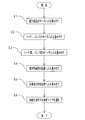
- FIG. 4 is a flowchart of the inspection area determination method of the present embodiment.
- FIG. 5 is a schematic diagram of the weighting work performed in step 1 of FIG.
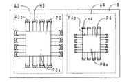
- FIG. 6 is a schematic diagram (part 1) of the weighting work performed in step 2 of FIG.
- FIG. 7 is a schematic diagram (part 2) of the weighting work performed in step 2 of FIG.
- FIG. 8 is a schematic diagram (part 1) of the weighting work performed in step 3 of FIG.
- FIG. 9 is a schematic diagram (part 2) of the weighting work performed in step 3 of FIG.
- FIG. 10 is a schematic diagram of the weighting work performed in step 4 of FIG.
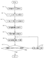
- FIG. 11 is a flowchart of the inspection area determination method of the second embodiment.
- Solder inspection machine (board inspection machine).
- 90: Screen printing machine 91: Electronic component mounting machine, 92: Substrate visual inspection machine, 93: Reflow furnace, 94: Host control device.
- A1 to A12 inspection area
- B substrate
- C7 to C10 pitch
- C11 distance
- C13 distance
- D7 to D11 pitch
- D13 pitch
- H1 to H14 pad
- L1 to L3 correlation line
- P1 to P14 Electronic component
- P3a Component body
- P3b Lead
- P4a Component body
- P4b Lead
- P5a Component body
- P5b Bump
- P6a Component body
- P6b Bump
- P7a Component body
- P6b Bump
- P7a Component body
- P7b Lead
- P8a component main body
- P8b lead
- P9a component main body
- P9b bump
- P10a component main body
- P10b bump
- S1 to S8 steps.
- FIG. 1 shows a schematic diagram of a production line in which the solder inspection machine of this embodiment is arranged.
- the production line 9 includes a screen printing machine 90, a solder inspection machine 1, a plurality of electronic component mounting machines 91, a board appearance inspection machine 92, and a reflow furnace 93 from the left side (upstream side) to the right side. They are lined up (downstream).
- each work machine arranged in the production line 9 is electrically connected to the host control device 94.
- solder is printed on the board. That is, the screen printer 90 includes a screen mask (not shown).
- the screen mask has a plurality of holes formed in a predetermined pattern. Solder is printed on the substrate through the plurality of holes. Pads (solder parts) are formed in a predetermined pattern on the substrate.
- the solder inspection machine 1 the printed state of the pads on the board is inspected.
- the plurality of electronic component mounting machines 91 a plurality of electronic components are mounted on the board.
- the board appearance inspection machine 92 the mounting state of the electronic component on the board is inspected.
- the substrate is heated. At this time, the solder forming the pad melts. After heating, the substrate is cooled to solidify the molten solder. At this time, the substrate and the electronic component are joined. In this way, the substrate is produced on the production line 9.
- FIG. 2 shows a top view of the solder inspection machine of the present embodiment.
- FIG. 3 shows a block diagram of the solder printer.
- the solder inspection machine 1 of the present embodiment includes a substrate transfer device 3, an XY robot 4, an inspection head 5, an imaging device 6, a control device 7, a base 80, An image processing device 81.
- the base 80 is disposed on the floor of the factory.
- the substrate transfer device 3 is disposed near the center of the upper surface of the base 80 in the front-rear direction.
- the substrate transfer device 3 includes a pair of front and rear wall portions 30, the pair of belts 31, and a transfer motor 33.
- the pair of front and rear wall portions 30 are erected on the upper surface of the base 80.
- the wall part 30 is extended in the left-right direction.
- the pair of front and rear belts 31 are disposed to face the rear surface of the front wall portion 30 and the front surface of the rear wall portion 30.
- the belt 31 extends in the left-right direction.
- the conveyance motor 33 drives a pair of front and rear belts 31. That is, the transport motor 33 transports the substrate B from the left side to the right side.
- the XY robot 4 includes a pair of front and rear X-axis guide rails 40, an X-axis slide 41, an X-axis motor 42, a pair of upper and lower Y-axis guide rails 43, a Y-axis slide 44, and a Y-axis motor 45. I have.
- the pair of front and rear X-axis guide rails 40 are disposed on the upper surface of the base 80.
- the X-axis guide rail 40 extends in the left-right direction.
- the X-axis slide 41 is slidable in the left-right direction with respect to the pair of front and rear X-axis guide rails 40.
- the X-axis motor 42 drives the X-axis slide 41 via a ball screw mechanism (not shown).
- the pair of upper and lower Y-axis guide rails 43 are arranged on the right surface of the X-axis slide 41.
- the Y-axis guide rail 43 extends in the front-rear direction.
- the Y-axis slide 44 can slide in the front-rear direction with respect to the pair of upper and lower Y-axis guide rails 43.
- the Y axis motor 45 drives the Y axis slide 44 via a ball screw mechanism (not shown).
- the inspection head 5 is attached to the right surface of the Y-axis slide 44.
- the imaging device 6 includes a CCD camera.
- the imaging device 6 is disposed on the lower surface of the inspection head 5.
- the imaging device 6 can image a plurality of inspection areas (not shown) of the substrate B from above.
- the control device 7 includes a calculation unit 70, a storage unit 71, an input / output interface 72, and a plurality of drive circuits.
- the input / output interface 72 is electrically connected to the transport motor 33, the X-axis motor 42, the Y-axis motor 45, and the imaging device 6 via a drive circuit.
- the input / output interface 72 is electrically connected to the image processing apparatus 81. Further, the image processing device 81 is electrically connected to the imaging device 6.
- the image processing device 81 processes the image data acquired by the imaging device 6.
- the solder inspection machine 1 inspects the printing state of the pads on the substrate B. Specifically, first, an inspection area to be inspected is selected from a plurality of preset inspection areas by using an inspection area determination method described later. Next, an inspection is performed on the selected inspection area using an inspection method described later.
- an inspection area to be inspected is selected from a plurality of preset inspection areas.
- the inspection area determination method includes a weighting step and an inspection area selection step.
- FIG. 4 shows a flowchart of the inspection area determination method. Steps 1 (S1) to 5 (S5) in FIG. 4 correspond to weighting steps. Step 6 (S6) in FIG. 4 corresponds to the inspection area selection step. Table 1 shows a weighting table used in the weighting step.
- Step 1 (S1) In the weighting step, first, the calculation unit 70 of the control device 7 shown in FIG. 3 refers to the shape data in the storage unit 71 and performs weighting according to the size of the electronic component (step 1 (S1) in FIG. 4).
- FIG. 5 shows a schematic diagram of the weighting work performed in step 1 of FIG.
- the electronic component P1 is scheduled to be arranged in the electronic component mounting machine 91 (disposed on the downstream side of the solder inspection machine 1) shown in FIG.
- the electronic component P2 is scheduled to be arranged in the electronic component mounter 91 shown in FIG.
- the electronic component P1 has a larger area when viewed from the upper side of the substrate B than the electronic component P2. That is, the size of the electronic component P1 is larger than that of the electronic component P2.
- the size of the pad H1 for the large electronic component P1 is often larger than the size of the pad H2 for the small electronic component P2.
- the pads H1 and H2 are formed by the screen printer 90 shown in FIG. Specifically, the pads H1 and H2 are formed by printing the solder on the upper surface of the substrate B through the holes of the screen mask. For this reason, compared with the case where the size of the hole is large (corresponding to the pad H1), the smaller the size of the hole (corresponding to the pad H2), the solder is more difficult to come out. Therefore, the pad H2 is more likely to be in a poor printing state than the pad H1.
- the inspection area A2 in which the small electronic component P2 is to be arranged has a higher priority for inspection than the inspection area A1 in which the large electronic component P1 is to be arranged. Focusing on this point, in step 1 of FIG. 4, weighting is performed according to the size of the electronic component.
- all electronic components to be arranged on the substrate B have five classes for each size (however, in the case of an electronic component having a component main body and a conductive portion, the size of the component main body). It is divided into. That is, the size of the largest electronic component and the size of the smallest electronic component are divided into five equal parts. Weight values 1 to 5 are assigned to the five classes. Specifically, weight values 1, 2, 3, 4, and 5 are assigned in order from the larger electronic component size toward the smaller size.
- the inspection area A2 is more in the inspection area A1.
- the weight value becomes larger than In other words, from the viewpoint of the sizes of the electronic components P1 and P2, the inspection area A2 has a higher inspection priority than the inspection area A1.
- Step 2 (S2) Next, in the weighting step, the calculation unit 70 of the control device 7 shown in FIG. 3 refers to the shape data in the storage unit 71 and performs weighting based on the lead and bump sizes (step 2 (S2) in FIG. 4). ).
- the lead and the bump are each included in the concept of the “conducting portion” of the present invention.
- FIG. 6 shows a schematic diagram (part 1) of the weighting work performed in step 2 of FIG.
- the electronic component P3 is scheduled to be arranged in the electronic component mounter 91 shown in FIG.
- the electronic component P4 is scheduled to be arranged in the electronic component mounter 91 shown in FIG.
- the electronic component P3 includes a component main body P3a and 16 leads P3b.
- the electronic component P4 includes a component main body P4a and 16 leads P4b.
- the lead P3b of the electronic component P3 has a larger area when viewed from above the substrate B than the lead P4b of the electronic component P4. That is, the lead P3b of the electronic component P3 is larger in size than the lead P4b of the electronic component P4.
- the pad H3 for the large lead P3b is often larger in size than the pad H4 for the small lead P4b.
- the pads H3 and H4 are formed by the screen printer 90 shown in FIG. Specifically, the pads H3 and H4 are formed by printing solder on the upper surface of the substrate B through the holes of the screen mask. For this reason, compared with the case where the size of the hole is large (corresponding to the pad H3), the smaller the hole size (corresponding to the pad H4), the solder is more difficult to come out from the hole. Therefore, the pad H4 is likely to be in a poorer printing state than the pad H3.
- the inspection priority of the inspection area A4 where the electronic component P4 including the small lead P4b is to be disposed is higher than the inspection area A3 where the electronic component P3 including the large lead P3b is to be disposed. Is expensive. Focusing on this point, in step 2 of FIG. 4, weighting is performed by lead of the electronic component.
- FIG. 7 shows a schematic diagram (part 2) of the weighting work performed in step 2 of FIG.
- the electronic component P5 is scheduled to be arranged in the electronic component mounter 91 shown in FIG.
- the electronic component P6 is scheduled to be arranged in the electronic component mounter 91 shown in FIG.
- the electronic component P5 includes a component body P5a and 16 bumps P5b.
- the electronic component P6 includes a component main body P6a and 16 bumps P6b.
- the bump P5b of the electronic component P5 has a larger area when viewed from the upper side of the substrate B than the bump P6b of the electronic component P6. That is, the size of the bump P5b of the electronic component P5 is larger than the size of the bump P6b of the electronic component P6.
- the pad H5 for the large bump P5b is often larger in size than the pad H6 for the small bump P6b.
- the pads H5 and H6 are formed by the screen printer 90 shown in FIG. Specifically, the solder H is printed on the upper surface of the substrate B through the holes of the screen mask, thereby forming the pads H5 and H6. For this reason, compared with the case where the size of the hole is large (corresponding to the pad H5), the smaller the hole size (corresponding to the pad H6), the solder is more difficult to come out from the hole. Therefore, the pad H6 is likely to be in a poorer printing state than the pad H5.
- the inspection area A6 where the electronic component P6 including the small bumps P6b is to be disposed has a higher priority for inspection than the inspection area A5 where the electronic component P5 including the large bumps P5b is to be disposed. Is expensive. Focusing on this point, in step 2 of FIG. 4, weighting by bumps of electronic components is performed.
- all electronic components to be arranged on the substrate B are divided into five classes according to the size of leads and bumps. That is, the largest lead / bump size and the smallest lead / bump size are divided into five equal parts. Weight values 1 to 5 are assigned to the five classes. Specifically, weight values 1, 2, 3, 4, and 5 are assigned in order from the larger lead and bump sizes to the smaller side.
- the size of the lead P4b is smaller than the size of the lead P3b, and therefore the inspection area A4 is larger than the inspection area A3.
- the weight value increases. That is, from the viewpoint of the size of the leads P3b and P4b, the inspection area A4 has a higher inspection priority than the inspection area A3.
- the inspection area A6 is larger than the inspection area A5.
- the weight value increases. That is, from the viewpoint of the size of the bumps P5b and P6b, the inspection area A6 has a higher inspection priority than the inspection area A5.
- weighting is not performed in the case of electronic components that do not have leads and bumps, such as the electronic components P1 and P2 shown in FIG.
- Step 3 (S3) Next, in the weighting step, the calculation unit 70 of the control device 7 shown in FIG. 3 refers to the shape data in the storage unit 71 and performs weighting according to the pitch between adjacent leads and the pitch between adjacent bumps ( Step 3 (S3) of FIG.
- FIG. 8 shows a schematic diagram (part 1) of the weighting work performed in step 3 of FIG.
- the electronic component P7 is to be arranged in the electronic component mounting machine 91 shown in FIG.
- the electronic component P8 is scheduled to be arranged in the electronic component mounter 91 shown in FIG.
- the electronic component P7 includes a component main body P7a and twelve leads P7b.
- the electronic component P8 includes a component main body P8a and 16 leads P8b.
- the pitch C7 between the adjacent leads P7b of the electronic component P7 is wider than the pitch C8 between the adjacent leads P8b of the electronic component P8.
- the pitch C7 between the adjacent leads P7b corresponds to the pitch D7 between the adjacent pads H7.
- the pitch D8 between the adjacent pads H8 corresponds to the pitch C8 between the adjacent leads P8b.
- the pitch D7 corresponding to the wide pitch C7 is often wider than the pitch D8 corresponding to the narrow pitch C8.
- the pads H7 and H8 are formed by the screen printer 90 shown in FIG. Specifically, the solder H is printed on the upper surface of the substrate B through the holes of the screen mask, so that the pads H7 and H8 are formed. For this reason, compared with the case where the pitch between adjacent holes is wide (corresponding to the pitch D7 between adjacent pads H7), the one where the pitch between adjacent holes is narrow (corresponding to the pitch D8 between adjacent pads H8). ) And bridge (connection between pads) is more likely to occur. Therefore, the pad H8 is likely to be in a poorer printing state than the pad H7.
- the inspection area A8 in which the electronic component P8 having a narrow pitch C8 between adjacent leads P8b is to be arranged is arranged in the inspection area in which the electronic component P7 having a wide pitch C7 between adjacent leads P7b is arranged.
- the priority of inspection is higher than A7. Focusing on this point, in step 3 of FIG. 4, weighting is performed by the pitch between leads of the electronic component.
- FIG. 9 shows a schematic diagram (part 2) of the weighting work performed in step 3 of FIG.
- the electronic component P9 is scheduled to be arranged in the electronic component mounter 91 shown in FIG.
- the electronic component P10 is scheduled to be arranged in the electronic component mounter 91 shown in FIG.
- the electronic component P9 includes a component main body P9a and nine bumps P9b.
- the electronic component P10 includes a component body P10a and 16 bumps P10b.
- the pitch C9 between the adjacent bumps P9b of the electronic component P9 is wider than the pitch C10 between the adjacent bumps P10b of the electronic component P10.
- the pitch C9 between the adjacent bumps P9b corresponds to the pitch D9 between the adjacent pads H9.
- the pitch D10 between the adjacent pads H10 corresponds to the pitch C10 between the adjacent bumps P10b.
- the pitch D9 corresponding to the wide pitch C9 is often wider than the pitch D10 corresponding to the narrow pitch C10.
- the pads H9 and H10 are formed by the screen printer 90 shown in FIG. Specifically, the pads H9 and H10 are formed by printing solder on the upper surface of the substrate B through the holes of the screen mask. For this reason, compared with the case where the pitch between adjacent holes is wide (corresponding to the pitch D9 between adjacent pads H9), the one where the pitch between adjacent holes is narrow (corresponding to the pitch D10 between adjacent pads H10). ) And bridge (connection between pads) is more likely to occur. Therefore, the pad H10 is likely to be in a poorer printing state than the pad H9.
- the inspection area A10 in which the electronic component P10 having a narrow pitch C10 between adjacent bumps P10b is to be arranged is in the inspection area in which the electronic component P9 having a wide pitch C9 between adjacent bumps P9b is to be arranged.
- the priority of inspection is higher than A9. Focusing on this point, in step 3 of FIG. 4, weighting is performed by the pitch between the bumps of the electronic component.
- weight values 1 to 5 are assigned to the five classes. Specifically, the weight values 1, 2, 3, 4, and 5 are assigned in order from the wide side to the narrow side where the pitch between adjacent leads and the pitch between adjacent bumps are narrow.
- the inspection area A8 is more weighted than the inspection area A7. Becomes larger. That is, from the viewpoint of the pitches C7 and C8 between the adjacent leads P7b and P8b, the inspection area A8 has a higher inspection priority than the inspection area A7.
- the inspection area A10 is weighted more than the inspection area A9. Becomes larger. That is, from the viewpoint of the pitches C9 and C10 between the adjacent bumps P9b and P10b, the inspection area A10 has a higher inspection priority than the inspection area A9.
- weighting is not performed in the case of an electronic component that does not have leads and bumps, such as the electronic components P1 and P2 shown in FIG.
- Step 4 (S4) Next, in the weighting step, the calculation unit 70 of the control device 7 shown in FIG. 3 refers to the inter-component distance data in the storage unit 71 and performs weighting according to the distance between adjacent electronic components (step in FIG. 4). 4 (S4)).
- FIG. 10 shows a schematic diagram of the weighting work performed in step 4 of FIG.
- the electronic components P11 and P12 are scheduled to be arranged in the electronic component mounter 91 shown in FIG.
- electronic components P13 and P14 are scheduled to be arranged in the electronic component mounter 91 shown in FIG.
- the distance C11 between the adjacent electronic components P11 and P12 is longer than the distance C13 between the adjacent electronic components P13 and P14.
- the distance C11 between the adjacent electronic components P11 and P12 corresponds to the pitch D11 between the adjacent pads H11 and H12.
- the distance C13 between the adjacent electronic components P13 and P14 corresponds to the pitch D13 between the adjacent pads H13 and H14.
- the pitch D11 corresponding to the long distance C11 is often wider than the pitch D13 corresponding to the short distance C13.
- the pads H11 to H14 are formed by the screen printer 90 shown in FIG. Specifically, the solder is printed on the upper surface of the substrate B through the holes of the screen mask, thereby forming the pads H11 to H14. For this reason, compared with the case where the pitch between adjacent holes is wide (corresponding to the pitch D11 between adjacent pads H11 and H12), the one where the pitch between adjacent holes is narrow (between adjacent pads H13 and H14). Corresponding to the pitch D13), the bridge (connection between pads) is more likely to occur. Therefore, the pads H13 and H14 are likely to be in a poorer printing state than the pads H11 and H12.
- the inspection area A12 in which the distance C13 between the electronic components P13 and P14 to be arranged is short has a higher inspection priority than the inspection area A11 in which the distance C11 between the electronic components P11 and P12 to be arranged is long. . Focusing on this point, in step 4 of FIG. 4, weighting is performed according to the distance between the electronic components.
- all electronic components scheduled to be arranged on the substrate B have a distance between adjacent electronic components (however, at least one of the adjacent electronic components includes a component main body and a conduction portion.
- the distance standard is divided into five classes for each electronic component). That is, the longest distance and the shortest distance are divided into five equal parts.
- Weight values 1 to 5 are assigned to the five classes. Specifically, weight values 1, 2, 3, 4, and 5 are assigned in order from the longer distance between adjacent electronic components to the shorter distance.
- the inspection area A12 is weighted more than the inspection area A11. Becomes larger. That is, from the viewpoint of the distances C11 and C13 between the adjacent electronic components P11 to P14, the inspection area A12 has a higher inspection priority than the inspection area A11.
- Step 5 (S5) Next, in the weighting step, the calculation unit 70 of the control device 7 shown in FIG. 3 performs weighting with reference to the manual setting data in the storage unit 71 (step 5 (S5) in FIG. 4). That is, as shown in Table 1, all electronic components scheduled to be placed on the board B are required to be inspected (indicated as “O” in Table 1) and inspected arbitrarily (indicated as “X” in Table 1). Divided into two classes.
- Step 6 (S6) In the inspection area selection step, the calculation unit 70 of the control device 7 shown in FIG. 3 adds up the weight values in steps 1 to 4 in FIG. 4 for every inspection area. Then, the sum of the weight values is compared with the threshold value in the storage unit 71. As a result of the comparison, when the sum exceeds the threshold value, the inspection area is selected as an inspection area for executing the inspection. When the sum is equal to or less than the threshold value, the inspection area is selected as an inspection area where no inspection is performed.
- the inspection area classified as “ ⁇ ” in step 5 the inspection area is always selected as the inspection area for executing the inspection regardless of the sum of the weight values from steps 1 to 4 in FIG.
- the inspection method the inspection area selected by the inspection area determination method (step 1 to step 6 in FIG. 4) is inspected.
- the control device 7 shown in FIG. 3 drives the X-axis motor 42 and the Y-axis motor 45 to move the inspection head 5 shown in FIG. 2 to the upper side of the inspection area to be inspected.
- the control device 7 illustrated in FIG. 3 drives the imaging device 6 to acquire an image of the inspection area.
- the image is processed by the image processing device 81 and transmitted to the control device 7.
- the control device 7 inspects the printing state of the pad in the inspection area from the image. In this method, the above series of operations is executed for all inspection areas selected by the inspection area determination method.
- the effect of the solder inspection machine of this embodiment is demonstrated.
- the part related data shape data, inter-part distance data, manual setting data
- a weighting operation relating to the inspection priority is performed on the plurality of inspection areas A1 to A12.
- inspection area selection step step 6 in FIG. 4
- inspection areas A1 to A12 for performing the inspection are selected based on the result of the weighting work. Therefore, the inspection areas A1 to A12 can be selected based on the component related data.
- the inspection areas A1 to A12 are determined based on the component-related data determined before the board production. This simplifies the circuit configuration and electrical processing compared to the case where the inspection areas A1 to A12 are determined based on the history of replacement work performed on the substrate B.
- the shape data includes the sizes of the electronic components P1 and P2.
- the inspection areas A1 and A2 for executing the inspection can be selected based on the sizes of the electronic components P1 and P2.
- the shape data includes the sizes of the leads P3b and P4b, and the bumps P5b and P6b.
- the inspection areas A3 to A6 for performing the inspection can be selected based on the sizes of the leads P3b and P4b and the bumps P5b and P6b.
- the shape data includes the pitches C7 and C8 between the adjacent leads P7b and P8b, and between the adjacent bumps P9b and P10b. Pitches C9 and C10.
- the narrower the pitch C7 to C10 the higher the possibility that the printing accuracy during printing of the pads H7 to H10 will be lowered. Therefore, the smaller the pitches C7 to C10, the higher the inspection priority.
- the inspection areas A7 to A10 for performing the inspection can be selected based on the widths of the pitches C7 to C10.
- the inter-component distance data includes the distances C11 and C13 between the adjacent electronic components P11 to P14.
- the shorter the distances C11 and C13 the higher the possibility that the printing accuracy during printing of the pads H11 to H14 will be lowered. For this reason, the shorter the distances C11 and C13, the higher the priority of inspection.
- the inspection areas A11 and A12 for performing the inspection can be selected based on the lengths of the distances C11 and C13.
- the component-related data includes manually set data. For this reason, an operator's intention can be reflected in weighting work.
- the inspection areas A1 to A12 for performing the inspection can be determined according to individual specific factors such as the inspection areas A1 to A12 in which the important electronic components P1 to P14 are arranged.
- each item of the component-related data is associated with a weight value related to the priority of inspection.
- a weight value is calculated for each of the inspection areas A1 to A12 and for each item.
- the inspection area selection step the sum of the weight values is calculated for each of the inspection areas A1 to A12. According to the solder inspection machine 1 of the present embodiment, the inspection areas A1 to A12 for executing the inspection can be selected by comparing the sum of the weight values with the threshold value.
- FIG. 11 shows a flowchart of the inspection area determination method of the present embodiment.
- part corresponding to FIG. 4 it shows with the same code
- step 9 an examination area that gives priority to examination is selected in consideration of the cycle time.
- step 10 the control device 7 operates the work machine (screen printing machine 90, a plurality of electronic component mounting machines 91, the board appearance) constituting the production line 9.
- the maximum cycle time is compared with the inspection time for the selected inspection area.
- the control device 7 adds one inspection area for executing the inspection (step 11 (S11)).
- the control device 7 repeatedly executes the addition of the inspection area until the maximum cycle time and the inspection time match at step 10.
- the addition of the inspection area in step 11 is performed in descending order of the sum of the weight values.
- the solder inspection machine according to the present embodiment and the solder inspection machine according to the first embodiment have the same functions and effects with respect to parts having the same configuration. Further, according to the inspection area selection step of the inspection area determination method of the present embodiment, the inspection area to be inspected is selected based on the cycle time required for the production of the substrate. For this reason, it is possible to increase the inspection area in which the inspection is performed within a range where the cycle time does not become long.
- Table 2 shows a weighting table used in the weighting step.
- the weight values may be different between the items. Further, the number of classes (number of divisions) may be different between the items. In addition, the increase / decrease amount of the weight value between the plurality of classes may not be constant between the items. Further, the amount of increase / decrease in the weight value between a plurality of classes within a single item may not be constant.
- FIG. 12 shows a correlation diagram between the size of electronic components and the weight value.
- the step-like correlation line L1 shown in FIG. 12 corresponds to the change in the weight value of the item “size of electronic component” in Table 1.
- the weight value may be changed stepwise with respect to the difference in the size of the electronic component.
- the weight value may be changed linearly with respect to the difference in the size of the electronic component.
- the weight value may be changed in a curved line with respect to the difference in the size of the electronic component.
- weighting such as the correlation line L3 is effective.
- items other than the “electronic component size” shown in Table 1 can be weighted as shown by correlation lines L1 to L3.
- the storage unit 71 stores the shape data, the inter-part distance data, the manual setting data, all the inspection areas for the board B, the weighting table shown in Table 1, and the sum of the weight values. Stored threshold.
- the above-mentioned various data are stored in the host control device 94, the screen printing machine 90 control device, the electronic component mounting machine 91 control device, the board appearance inspection machine 92 control device, and the reflow furnace control device shown in FIG. May be.
- step 1 to step 5 in FIG. 4 is not particularly limited. In step 6, it is sufficient if the sum of the weight values in steps 1 to 4 can be calculated.
- the inspection area may be selected as the inspection area to be inspected regardless of the sum of the weight values.
- the configuration and movement of the board visual inspection machine 92 are the same as those of the solder inspection machine 1 (FIGS. 2 and 3) of the first embodiment.
Landscapes
- Engineering & Computer Science (AREA)
- Manufacturing & Machinery (AREA)
- Microelectronics & Electronic Packaging (AREA)
- Operations Research (AREA)
- Electric Connection Of Electric Components To Printed Circuits (AREA)
- Image Processing (AREA)
Description
本発明は、例えば、基板に対するはんだの印刷状態を検査するはんだ検査、基板に対する電子部品の装着状態を検査する基板外観検査などに用いられる検査エリア決定方法に関する。また、本発明は、上記はんだ検査を行うはんだ検査機、上記基板外観検査を行う基板外観検査機などの基板検査機に関する。
基板の生産ラインにおいては、上流側から下流側に向かって、スクリーン印刷機と、はんだ検査機と、電子部品実装機と、基板外観検査機と、リフロー炉と、が並んでいる。このうち、はんだ検査機は、基板に対するはんだの印刷状態を検査している。すなわち、スクリーン印刷機においては、基板に、スクリーンマスクの孔を介して、はんだが印刷される。ここで、印刷精度(スクリーンマスクの孔形状に対する、基板に印刷されたはんだ形状の再現度)が低い場合、つまり印刷状態が悪い場合、電子部品実装後の基板に、導通不良などの不具合が発生するおそれがある。このため、はんだ検査機は、はんだの印刷状態を検査している。
しかしながら、基板の全ての検査エリアに対して検査を行うと、その分、基板一枚あたりの検査時間が長くなってしまう。また、はんだ検査機が生産ラインのボトルネックとなってしまい、はんだ検査機の下流側の作業機(例えば、電子部品実装機)において、「基板搬入待ち」の状態(上流側の作業機から基板が搬入されるのを、下流側の作業機が待っている状態)になることも考えられる。
そこで、特許文献1には、検査エリアを選択可能な基板外観検査機が開示されている。電子部品実装機においては、電子部品搬送用の吸着ノズルの変更や、電子部品供給用のテープフィーダの変更などの、変更作業を行う場合がある。基板外観検査機は、当該変更作業が行われた場合に、変更作業に関連する検査エリアを、検査を実行する検査エリアとして、優先的に選択している。このため、基板の全ての検査エリアに対して検査を行う場合と比較して、基板一枚あたりの検査時間を短縮することができる。
このように、同文献には、交換作業の履歴を基に、検査エリアを選択する方法が開示されている。つまり、実際に行われた作業の履歴を基に、検査エリアを選択する方法が開示されている。しかしながら、作業履歴以外にも、検査エリアを選択する基準になる因子は存在する。
そこで、本発明は、電子部品の形状や、隣り合う二つの電子部品間の距離などの部品関連データを基に、検査エリアを選択可能な検査エリア決定方法、および基板検査機を提供することを目的とする。
(1)上記課題を解決するため、本発明の検査エリア決定方法は、基板に装着される電子部品の形状に関する形状データ、該電子部品と該電子部品に隣り合う別の電子部品との間の距離に関する部品間距離データのうち、少なくとも一つを含む部品関連データを基に、予め該基板に設定される複数の検査エリアに対して、検査の優先度に関する重み付け作業を行う重み付けステップと、該重み付け作業の結果を基に、複数の該検査エリアから、該検査を実行する該検査エリアを選択する検査エリア選択ステップと、を有することを特徴とする。
部品関連データは、形状データおよび部品間距離データのうち、少なくとも一つを含んでいる。形状データは、電子部品の形状(導通部(リード、バンプなど)の形状を含む)に関するデータである。部品間距離データは、隣り合う電子部品間の距離に関するデータである。形状データ、部品間距離データは、基板の設計に関するデータである。このため、形状データ、部品間距離データは、基板生産前に、既に決定されている。
本発明の検査エリア決定方法によると、まず、重み付けステップにおいて、部品関連データを基に、複数の検査エリアに対して、検査の優先度に関する重み付け作業を行っている。次に、検査エリア選択ステップにおいて、重み付け作業の結果を基に、検査を実行する検査エリア(単一でも、複数でもよい。)を選択している。このため、部品関連データを基に、検査エリアを選択することができる。
本発明の検査エリア決定方法によると、基板生産前に決定済みの部品関連データを基に、検査エリアを決定している。このため、基板に対して行われた交換作業の履歴を基に検査エリアを決定する場合と比較して、電気的な処理が簡単になる。
(2)好ましくは、上記(1)の構成において、前記形状データは、前記電子部品のサイズを含む構成とする方がよい。
本構成によると、電子部品のサイズ(基板の上側から見た場合の電子部品のサイズ。電子部品が、部品本体と、部品本体と基板との間の導通を確保する導通部と、を有する場合は、基板の上側から見た場合の部品本体のサイズ。)を基に、検査を実行する検査エリアを選択している。すなわち、電子部品のサイズが大きい場合、当該電子部品に対応する基板のパッド(はんだ部)のサイズも大きくなる。パッドが大きいほど、印刷時に、「欠け」、「かすれ」などの印刷不良が発生しにくくなる。このため、電子部品のサイズが大きいほど、検査の優先度は低くなる。反対に、電子部品のサイズが小さい場合、基板のパッドのサイズも小さくなる。パッドのサイズが小さいほど、印刷不良が発生しやすくなる。このため、電子部品のサイズが小さいほど、検査の優先度は高くなる。このように、本構成によると、検査エリアに装着される電子部品のサイズを基に、検査を実行する検査エリアを選択することができる。
(3)好ましくは、上記(1)または(2)の構成において、前記電子部品は、部品本体と、該部品本体と前記基板との間の導通を確保する導通部と、を有し、前記形状データは、該導通部のサイズを含む構成とする方がよい。
本構成によると、導通部のサイズ(基板の上側から見た場合の導通部のサイズ)を基に、検査を実行する検査エリアを選択している。すなわち、導通部のサイズが大きい場合、当該導通部に対応する基板のパッドのサイズも大きくなる。パッドが大きいほど、印刷不良が発生しにくくなる。このため、導通部のサイズが大きいほど、検査の優先度は低くなる。反対に、導通部のサイズが小さい場合、基板のパッドのサイズも小さくなる。パッドのサイズが小さいほど、印刷不良が発生しやすくなる。このため、導通部のサイズが小さいほど、検査の優先度は高くなる。このように、本構成によると、検査エリアに装着される電子部品の導通部のサイズを基に、検査を実行する検査エリアを選択することができる。
(4)好ましくは、上記(1)ないし(3)のいずれかの構成において、前記電子部品は、部品本体と、該部品本体と前記基板との間の導通を確保する複数の導通部と、を有し、前記形状データは、複数の該導通部の間のピッチを含む構成とする方がよい。
本構成によると、複数の導通部の間のピッチ(基板の上側から見た場合の複数の導通部の間のピッチ)を基に、検査を実行する検査エリアを選択している。すなわち、複数の導通部の間のピッチが広い場合、当該ピッチに対応する、基板の複数のパッドの間のピッチも、広くなる。複数のパッドの間のピッチが広いほど、例えばブリッジなどの、印刷不良が発生しにくくなる。このため、複数のパッドの間のピッチが広いほど、検査の優先度は低くなる。反対に、複数の導通部の間のピッチが狭い場合、当該ピッチに対応する、基板の複数のパッドの間のピッチも狭くなる。複数のパッドの間のピッチが狭いほど、例えばブリッジなどの、印刷不良が発生しやすくなる。このため、複数のパッドの間のピッチが狭いほど、検査の優先度は高くなる。このように、本構成によると、検査エリアに装着される電子部品の、複数の導通部の間のピッチを基に、検査を実行する検査エリアを選択することができる。
(5)好ましくは、上記(1)ないし(4)のいずれかの構成において、前記部品関連データは、作業者が手動で設定する手動設定データを含む構成とする方がよい。本構成によると、作業者の意思を、重み付け作業に反映させることができる。このため、例えば、重要な電子部品が配置される検査エリアなど、個別具体的な要因に応じて、検査を実行する検査エリアを決定することができる。
(6)好ましくは、上記(1)ないし(5)のいずれかの構成において、前記部品関連データには、前記検査の優先度に関する重み値が関連付けられており、前記検査エリア選択ステップにおいては、該重み値の総和が所定のしきい値を超過する前記検査エリアを、該検査を実行する該検査エリアに選択する構成とする方がよい。本構成によると、重み値の総和と、しきい値と、を比較することにより、検査を実行する検査エリアを選択することができる。
(7)好ましくは、上記(1)ないし(6)のいずれかの構成において、前記検査エリア選択ステップにおいては、前記重み付け作業の結果に加えて、前記基板の生産に要するサイクルタイムを基に、前記検査を実行する前記検査エリアを選択する構成とする方がよい。
基板の生産ラインを構成する任意の作業機においては、「基板搬入待ち」(上流側の作業機から基板が搬入されるのを、下流側の作業機が待っている状態)、および「基板搬出待ち」の状態(下流側の作業機から基板が搬出されるのを、上流側の作業機が待っている状態)が発生する場合がある。
「基板搬出待ち」の状態が発生すると、その分、基板の生産(基板にはんだを印刷し、電子部品を装着し、はんだを溶融、固化させる作業)に要するサイクルタイムが長くなってしまう。
この点、本構成の検査エリア選択ステップによると、基板の生産に要するサイクルタイムを基に、検査を実行する検査エリアを選択している。具体的には、基板検査機以外の作業機のサイクルタイムに合わせて過度の「基板搬入待ち」および「基板搬出待ち」が発生しない程度に検査を実行する検査エリアを選択している。
また、実生産中に、既に任意の作業機において、「基板搬出待ち」の状態が発生している場合は、当該「基板搬出待ち」の状態が解消されるまでは、検査時間を長くすることができる。言い換えると、「基板搬入待ち」の状態が発生しない限度まで、検査時間を長くすることができる。このため、検査を実行する検査エリアを増やすことができる。すなわち、サイクルタイムが長くならない範囲で、検査エリアを増やすことができる。
(8)好ましくは、上記(1)ないし(7)のいずれかの構成において、前記検査は、前記基板に対するはんだの印刷状態の検査である構成とする方がよい。本構成によると、はんだの印刷状態の検査に関する複数の検査エリアの中から、検査を実行する検査エリアを、選択することができる。
(9)上記課題を解決するため、本発明の基板検査機は、基板に装着される電子部品の形状に関する形状データ、該電子部品と該電子部品に隣り合う別の電子部品との間の距離に関する部品間距離データのうち、少なくとも一つを含む部品関連データを基に、予め該基板に設定される複数の検査エリアに対して、検査の優先度に関する重み付け作業を行う重み付けステップと、該重み付け作業の結果を基に、複数の該検査エリアから、該検査を実行する該検査エリアを選択する検査エリア選択ステップと、を実行する制御装置と、選択された該検査エリアに対して検査を実行する検査ヘッドと、を備え、該基板に対して行われた作業の結果を検査することを特徴とする。
本発明の基板検査機によると、上記(1)の構成と同様に、部品関連データを基に、検査エリアを選択することができる。また、基板に対して行われた交換作業の履歴を基に検査エリアを決定する場合と比較して、電気的な処理が簡単になる。
(10)好ましくは、上記(9)の構成において、前記形状データは、前記電子部品のサイズを含む構成とする方がよい。本構成によると、上記(2)の構成と同様に、検査エリアに装着される電子部品のサイズを基に、検査を実行する検査エリアを選択することができる。
(11)好ましくは、上記(9)または(10)の構成において、前記電子部品は、部品本体と、該部品本体と前記基板との間の導通を確保する導通部と、を有し、前記形状データは、該導通部のサイズを含む構成とする方がよい。本構成によると、上記(3)の構成と同様に、検査エリアに装着される電子部品の導通部のサイズを基に、検査を実行する検査エリアを選択することができる。
(12)好ましくは、上記(9)ないし(11)のいずれかの構成において、前記電子部品は、部品本体と、該部品本体と前記基板との間の導通を確保する複数の導通部と、を有し、前記形状データは、複数の該導通部の間のピッチを含む構成とする方がよい。本構成によると、上記(4)の構成と同様に、検査エリアに装着される電子部品の、複数の導通部の間のピッチを基に、検査を実行する検査エリアを選択することができる。
(13)好ましくは、上記(9)ないし(12)のいずれかの構成において、前記部品関連データは、作業者が手動で設定する手動設定データを含む構成とする方がよい。本構成によると、上記(5)の構成と同様に、作業者の意思を、重み付け作業に反映させることができる。このため、例えば、重要な電子部品が配置される検査エリアなど、個別具体的な要因に応じて、検査を実行する検査エリアを決定することができる。
(14)好ましくは、上記(9)ないし(13)のいずれかの構成において、前記部品関連データには、前記検査の優先度に関する重み値が関連付けられており、前記検査エリア選択ステップにおいては、該重み値の総和が所定のしきい値を超過する前記検査エリアを、該検査を実行する該検査エリアに選択する構成とする方がよい。本構成によると、上記(6)の構成と同様に、重み値の総和と、しきい値と、を比較することにより、検査を実行する検査エリアを選択することができる。
(15)好ましくは、上記(9)ないし(14)のいずれかの構成において、前記検査エリア選択ステップにおいては、前記重み付け作業の結果に加えて、前記基板の生産に要するサイクルタイムを基に、前記検査を実行する前記検査エリアを選択する構成とする方がよい。
本構成によると、上記(7)の構成と同様に、基板の生産に要するサイクルタイムを基に、検査を実行する検査エリアを選択している。具体的には、基板検査機以外の作業機のサイクルタイムに合わせて過度の「基板搬入待ち」および「基板搬出待ち」が発生しない程度に検査を実行する検査エリアを選択している。
また、実生産中に、既に任意の作業機において、「基板搬出待ち」の状態が発生している場合は、当該「基板搬出待ち」の状態が解消されるまでは、検査時間を長くすることができる。言い換えると、「基板搬入待ち」の状態が発生しない限度まで、検査時間を長くすることができる。このため、検査を実行する検査エリアを増やすことができる。すなわち、サイクルタイムが長くならない範囲で、検査エリアを増やすことができる。
(16)好ましくは、上記(9)ないし(15)のいずれかの構成において、前記検査は、前記基板に対するはんだの印刷状態の検査である構成とする方がよい。本構成によると、上記(8)の構成と同様に、はんだの印刷状態の検査に関する複数の検査エリアの中から、検査を実行する検査エリアを、選択することができる。
本発明によると、部品関連データを基に、検査エリアを選択可能な検査エリア決定方法、および基板検査機を提供することができる。
1:はんだ検査機(基板検査機)。
3:基板搬送装置、30:壁部、31:ベルト、33:搬送モータ。
4:XYロボット、40:X軸ガイドレール、41:X軸スライド、42:X軸モータ、43:Y軸ガイドレール、44:Y軸スライド、45:Y軸モータ。
5:検査ヘッド。
6:撮像装置。
7:制御装置、70:演算部、71:記憶部、72:入出力インターフェイス。
80:ベース、81:画像処理装置。
9:生産ライン、90:スクリーン印刷機、91:電子部品実装機、92:基板外観検査機、93:リフロー炉、94:上位制御装置。
A1~A12:検査エリア、B:基板、C7~C10:ピッチ、C11:距離、C13:距離、D7~D11:ピッチ、D13:ピッチ、H1~H14:パッド、L1~L3:相関線、P1~P14:電子部品、P3a:部品本体、P3b:リード、P4a:部品本体、P4b:リード、P5a:部品本体、P5b:バンプ、P6a:部品本体、P6b:バンプ、P7a:部品本体、P7b:リード、P8a:部品本体、P8b:リード、P9a:部品本体、P9b:バンプ、P10a:部品本体、P10b:バンプ、S1~S8:ステップ。
3:基板搬送装置、30:壁部、31:ベルト、33:搬送モータ。
4:XYロボット、40:X軸ガイドレール、41:X軸スライド、42:X軸モータ、43:Y軸ガイドレール、44:Y軸スライド、45:Y軸モータ。
5:検査ヘッド。
6:撮像装置。
7:制御装置、70:演算部、71:記憶部、72:入出力インターフェイス。
80:ベース、81:画像処理装置。
9:生産ライン、90:スクリーン印刷機、91:電子部品実装機、92:基板外観検査機、93:リフロー炉、94:上位制御装置。
A1~A12:検査エリア、B:基板、C7~C10:ピッチ、C11:距離、C13:距離、D7~D11:ピッチ、D13:ピッチ、H1~H14:パッド、L1~L3:相関線、P1~P14:電子部品、P3a:部品本体、P3b:リード、P4a:部品本体、P4b:リード、P5a:部品本体、P5b:バンプ、P6a:部品本体、P6b:バンプ、P7a:部品本体、P7b:リード、P8a:部品本体、P8b:リード、P9a:部品本体、P9b:バンプ、P10a:部品本体、P10b:バンプ、S1~S8:ステップ。
以下、本発明の基板検査機をはんだ検査機として具現化した場合の実施の形態について説明する。なお、以下の説明は、本発明の検査エリア決定方法の実施の形態の説明を兼ねる。
<第一実施形態>
[生産ラインの構成]
まず、本実施形態のはんだ検査機が配置される生産ラインの構成について説明する。以下に示す図面において、左右方向は、X軸方向(基板の搬送方向)に対応している。前後方向は、Y軸方向(水平面内においてX軸方向に対して直交する方向)に対応している。
[生産ラインの構成]
まず、本実施形態のはんだ検査機が配置される生産ラインの構成について説明する。以下に示す図面において、左右方向は、X軸方向(基板の搬送方向)に対応している。前後方向は、Y軸方向(水平面内においてX軸方向に対して直交する方向)に対応している。
図1に、本実施形態のはんだ検査機が配置される生産ラインの模式図を示す。図1に示すように、生産ライン9には、スクリーン印刷機90とはんだ検査機1と複数の電子部品実装機91と基板外観検査機92とリフロー炉93とが、左側(上流側)から右側(下流側)に向かって、並んでいる。また、生産ライン9に配置された各作業機は、上位制御装置94に、電気的に接続されている。
スクリーン印刷機90においては、基板にはんだが印刷される。すなわち、スクリーン印刷機90は、スクリーンマスク(図略)を備えている。スクリーンマスクには、所定のパターンで、複数の孔が穿設されている。複数の孔を介して、はんだが基板に印刷される。基板には、所定のパターンで、パッド(はんだ部)が形成される。
はんだ検査機1においては、基板に対するパッドの印刷状態が検査される。複数の電子部品実装機91においては、基板に複数の電子部品が装着される。基板外観検査機92においては、基板に対する電子部品の装着状態が検査される。リフロー炉93においては、基板が加熱される。この際、パッドを形成するはんだが溶融する。加熱後、基板が冷却されることにより、溶融したはんだが固化する。この際、基板と電子部品とが接合される。このようにして、生産ライン9において基板が生産される。
[はんだ検査機の構成]
次に、本実施形態のはんだ検査機の構成について説明する。図2に、本実施形態のはんだ検査機の上面図を示す。図3に、同はんだ印刷機のブロック図を示す。図2、図3に示すように、本実施形態のはんだ検査機1は、基板搬送装置3と、XYロボット4と、検査ヘッド5と、撮像装置6と、制御装置7と、ベース80と、画像処理装置81と、を備えている。
次に、本実施形態のはんだ検査機の構成について説明する。図2に、本実施形態のはんだ検査機の上面図を示す。図3に、同はんだ印刷機のブロック図を示す。図2、図3に示すように、本実施形態のはんだ検査機1は、基板搬送装置3と、XYロボット4と、検査ヘッド5と、撮像装置6と、制御装置7と、ベース80と、画像処理装置81と、を備えている。
{ベース80、基板搬送装置3}
ベース80は、工場の床面に配置されている。基板搬送装置3は、ベース80の上面の前後方向中央付近に配置されている。基板搬送装置3は、前後一対の壁部30と、前記一対のベルト31と、搬送モータ33と、を備えている。
ベース80は、工場の床面に配置されている。基板搬送装置3は、ベース80の上面の前後方向中央付近に配置されている。基板搬送装置3は、前後一対の壁部30と、前記一対のベルト31と、搬送モータ33と、を備えている。
前後一対の壁部30は、ベース80の上面に立設されている。壁部30は、左右方向に延在している。前後一対のベルト31は、前側の壁部30の後面と、後側の壁部30の前面と、に対向して配置されている。ベルト31は、左右方向に延在している。基板搬送時において、基板Bは、前後一対のベルト31に架設されている。搬送モータ33は、前後一対のベルト31を駆動している。すなわち、搬送モータ33は、基板Bを、左側から右側に搬送している。
{XYロボット4}
XYロボット4は、前後一対のX軸ガイドレール40と、X軸スライド41と、X軸モータ42と、上下一対のY軸ガイドレール43と、Y軸スライド44と、Y軸モータ45と、を備えている。
XYロボット4は、前後一対のX軸ガイドレール40と、X軸スライド41と、X軸モータ42と、上下一対のY軸ガイドレール43と、Y軸スライド44と、Y軸モータ45と、を備えている。
前後一対のX軸ガイドレール40は、ベース80の上面に配置されている。X軸ガイドレール40は、左右方向に延在している。X軸スライド41は、前後一対のX軸ガイドレール40に対して、左右方向に摺動可能である。X軸モータ42は、ボールねじ機構部(図略)を介して、X軸スライド41を駆動している。
上下一対のY軸ガイドレール43は、X軸スライド41の右面に配置されている。Y軸ガイドレール43は、前後方向に延在している。Y軸スライド44は、上下一対のY軸ガイドレール43に対して、前後方向に摺動可能である。Y軸モータ45は、ボールねじ機構部(図略)を介して、Y軸スライド44を駆動している。
{検査ヘッド5、撮像装置6、制御装置7、画像処理装置81}
検査ヘッド5は、Y軸スライド44の右面に取り付けられている。撮像装置6は、CCDカメラを備えている。撮像装置6は、検査ヘッド5の下面に配置されている。撮像装置6は、基板Bの複数の検査エリア(図略)を上側から撮像可能である。
検査ヘッド5は、Y軸スライド44の右面に取り付けられている。撮像装置6は、CCDカメラを備えている。撮像装置6は、検査ヘッド5の下面に配置されている。撮像装置6は、基板Bの複数の検査エリア(図略)を上側から撮像可能である。
制御装置7は、演算部70と、記憶部71と、入出力インターフェイス72と、複数の駆動回路と、を備えている。入出力インターフェイス72は、搬送モータ33、X軸モータ42、Y軸モータ45、撮像装置6と、各々、駆動回路を介して、電気的に接続されている。また、入出力インターフェイス72は、画像処理装置81に、電気的に接続されている。また、画像処理装置81は、撮像装置6に、電気的に接続されている。画像処理装置81は、撮像装置6が取得した画像データを処理している。
[はんだ検査機の動き]
次に、本実施形態のはんだ検査機の動きについて説明する。はんだ検査機1は、基板Bに対するパッドの印刷状態を検査する。具体的には、まず、後述する検査エリア決定方法を用いて、予め設定されている複数の検査エリアの中から、検査を実行する検査エリアを選択する。次に、後述する検査方法を用いて、選択した検査エリアに対して、検査を実行する。
次に、本実施形態のはんだ検査機の動きについて説明する。はんだ検査機1は、基板Bに対するパッドの印刷状態を検査する。具体的には、まず、後述する検査エリア決定方法を用いて、予め設定されている複数の検査エリアの中から、検査を実行する検査エリアを選択する。次に、後述する検査方法を用いて、選択した検査エリアに対して、検査を実行する。
{検査エリア決定方法}
検査エリア決定方法においては、予め設定されている複数の検査エリアの中から、検査を実行する検査エリアを選択する。検査エリア決定方法は、重み付けステップと、検査エリア選択ステップと、を有している。
検査エリア決定方法においては、予め設定されている複数の検査エリアの中から、検査を実行する検査エリアを選択する。検査エリア決定方法は、重み付けステップと、検査エリア選択ステップと、を有している。
図4に、検査エリア決定方法のフローチャートを示す。図4のステップ1(S1)からステップ5(S5)は、重み付けステップに対応する。図4のステップ6(S6)は、検査エリア選択ステップに対応する。表1に、重み付けステップで用いられる重み付けテーブルを示す。

図3に示す制御装置7の記憶部71には、基板Bに装着される電子部品の形状に関する形状データ、隣り合う電子部品間の距離に関する部品間距離データ、作業者が手動で設定した手動設定データ、基板Bに対する全ての検査エリア、表1に示す重み付けテーブル、重み値の総和に対するしきい値が、格納されている。
(ステップ1(S1))
重み付けステップにおいては、まず、図3に示す制御装置7の演算部70が、記憶部71の形状データを参照して、電子部品のサイズによる重み付けを行う(図4のステップ1(S1))。
重み付けステップにおいては、まず、図3に示す制御装置7の演算部70が、記憶部71の形状データを参照して、電子部品のサイズによる重み付けを行う(図4のステップ1(S1))。
図5に、図4のステップ1で行われる重み付け作業の模式図を示す。検査エリアA1には、図1に示す電子部品実装機91(はんだ検査機1の下流側に配置されている)において、電子部品P1が配置される予定である。一方、検査エリアA2には、図1に示す電子部品実装機91において、電子部品P2が配置される予定である。ここで、図中太線で示すように、電子部品P1の方が、電子部品P2よりも、基板Bの上側から見た場合の面積が大きい。つまり、電子部品P1の方が、電子部品P2よりも、サイズが大きい。
この場合、大型の電子部品P1用のパッドH1の方が、小型の電子部品P2用のパッドH2よりも、サイズが大きい場合が多い。ここで、パッドH1、H2は、図1に示すスクリーン印刷機90により、形成される。具体的には、はんだが、スクリーンマスクの孔を介して、基板Bの上面に印刷されることにより、パッドH1、H2が形成される。このため、孔のサイズが大きい場合(パッドH1に対応)と比較して、孔のサイズが小さい方が(パッドH2に対応)、より孔からはんだが抜けにくくなる。したがって、パッドH2の方が、パッドH1よりも、印刷状態が悪い可能性が高い。言い換えると、小型の電子部品P2が配置される予定の検査エリアA2の方が、大型の電子部品P1が配置される予定の検査エリアA1よりも、検査の優先度が高い。この点に着目して、図4のステップ1においては、電子部品のサイズによる重み付けを行っている。
表1に示すように、基板Bに配置される予定の全電子部品は、サイズ(ただし、部品本体と、導通部と、を備える電子部品の場合は、部品本体のサイズ)ごとに五つの階級に分けられている。すなわち、最も大きい電子部品のサイズと、最も小さい電子部品のサイズと、の間を、五等分に分割している。五つの階級には、重み値1~5が割り当てられている。具体的には、電子部品のサイズが大きい側から小さい側に向かって、順番に、重み値1、2、3、4、5が割り当てられている。
表1に示す重み付けテーブルを用いて、図5に示す検査エリアA1、A2の重み付けを行う場合、電子部品P2の方が電子部品P1よりもサイズが小さいため、検査エリアA2の方が検査エリアA1よりも重み値が大きくなる。つまり、電子部品P1、P2のサイズという観点からは、検査エリアA2の方が、検査エリアA1よりも、検査の優先度が高くなる。
(ステップ2(S2))
重み付けステップにおいては、次に、図3に示す制御装置7の演算部70が、記憶部71の形状データを参照して、リード、バンプのサイズによる重み付けを行う(図4のステップ2(S2))。なお、リード、バンプは、各々、本発明の「導通部」の概念に含まれる。
重み付けステップにおいては、次に、図3に示す制御装置7の演算部70が、記憶部71の形状データを参照して、リード、バンプのサイズによる重み付けを行う(図4のステップ2(S2))。なお、リード、バンプは、各々、本発明の「導通部」の概念に含まれる。
図6に、図4のステップ2で行われる重み付け作業の模式図(その1)を示す。検査エリアA3には、図1に示す電子部品実装機91において、電子部品P3が配置される予定である。一方、検査エリアA4には、図1に示す電子部品実装機91において、電子部品P4が配置される予定である。電子部品P3は、部品本体P3aと、16本のリードP3bと、を備えている。同様に、電子部品P4は、部品本体P4aと、16本のリードP4bと、を備えている。ここで、図中太線で示すように、電子部品P3のリードP3bの方が、電子部品P4のリードP4bよりも、基板Bの上側から見た場合の面積が大きい。つまり、電子部品P3のリードP3bの方が、電子部品P4のリードP4bよりも、サイズが大きい。
この場合、大型のリードP3b用のパッドH3の方が、小型のリードP4b用のパッドH4よりも、サイズが大きい場合が多い。ここで、パッドH3、H4は、図1に示すスクリーン印刷機90により、形成される。具体的には、はんだが、スクリーンマスクの孔を介して、基板Bの上面に印刷されることにより、パッドH3、H4が形成される。このため、孔のサイズが大きい場合(パッドH3に対応)と比較して、孔のサイズが小さい方が(パッドH4に対応)、より孔からはんだが抜けにくくなる。したがって、パッドH4の方が、パッドH3よりも、印刷状態が悪い可能性が高い。言い換えると、小型のリードP4bを備える電子部品P4が配置される予定の検査エリアA4の方が、大型のリードP3bを備える電子部品P3が配置される予定の検査エリアA3よりも、検査の優先度が高い。この点に着目して、図4のステップ2においては、電子部品のリードによる重み付けを行っている。
図7に、図4のステップ2で行われる重み付け作業の模式図(その2)を示す。検査エリアA5には、図1に示す電子部品実装機91において、電子部品P5が配置される予定である。一方、検査エリアA6には、図1に示す電子部品実装機91において、電子部品P6が配置される予定である。図7に透過して示すように、電子部品P5は、部品本体P5aと、16個のバンプP5bと、を備えている。同様に、電子部品P6は、部品本体P6aと、16個のバンプP6bと、を備えている。ここで、図中太線で示すように、電子部品P5のバンプP5bの方が、電子部品P6のバンプP6bよりも、基板Bの上側から見た場合の面積が大きい。つまり、電子部品P5のバンプP5bの方が、電子部品P6のバンプP6bよりも、サイズが大きい。
この場合、大型のバンプP5b用のパッドH5の方が、小型のバンプP6b用のパッドH6よりも、サイズが大きい場合が多い。ここで、パッドH5、H6は、図1に示すスクリーン印刷機90により、形成される。具体的には、はんだが、スクリーンマスクの孔を介して、基板Bの上面に印刷されることにより、パッドH5、H6が形成される。このため、孔のサイズが大きい場合(パッドH5に対応)と比較して、孔のサイズが小さい方が(パッドH6に対応)、より孔からはんだが抜けにくくなる。したがって、パッドH6の方が、パッドH5よりも、印刷状態が悪い可能性が高い。言い換えると、小型のバンプP6bを備える電子部品P6が配置される予定の検査エリアA6の方が、大型のバンプP5bを備える電子部品P5が配置される予定の検査エリアA5よりも、検査の優先度が高い。この点に着目して、図4のステップ2においては、電子部品のバンプによる重み付けを行っている。
表1に示すように、基板Bに配置される予定の全電子部品は、リード、バンプのサイズごとに五つの階級に分けられている。すなわち、最も大きいリード、バンプのサイズと、最も小さいリード、バンプのサイズと、の間を、五等分に分割している。五つの階級には、重み値1~5が割り当てられている。具体的には、リード、バンプのサイズが大きい側から小さい側に向かって、順番に、重み値1、2、3、4、5が割り当てられている。
表1に示す重み付けテーブルを用いて、図6に示す検査エリアA3、A4の重み付けを行う場合、リードP4bの方がリードP3bよりもサイズが小さいため、検査エリアA4の方が検査エリアA3よりも重み値が大きくなる。つまり、リードP3b、P4bのサイズという観点からは、検査エリアA4の方が、検査エリアA3よりも、検査の優先度が高くなる。
表1に示す重み付けテーブルを用いて、図7に示す検査エリアA5、A6の重み付けを行う場合、バンプP6bの方がバンプP5bよりもサイズが小さいため、検査エリアA6の方が検査エリアA5よりも重み値が大きくなる。つまり、バンプP5b、P6bのサイズという観点からは、検査エリアA6の方が、検査エリアA5よりも、検査の優先度が高くなる。
なお、図5に示す電子部品P1、P2のように、リード、バンプを有しない電子部品の場合は、重み付けは行われない。言い換えると、リード、バンプを有しない電子部品の場合は、図4のステップ2に対応する表1の重み値=0になる。
(ステップ3(S3))
重み付けステップにおいては、次に、図3に示す制御装置7の演算部70が、記憶部71の形状データを参照して、隣り合うリード間のピッチ、隣り合うバンプ間のピッチによる重み付けを行う(図4のステップ3(S3))。
重み付けステップにおいては、次に、図3に示す制御装置7の演算部70が、記憶部71の形状データを参照して、隣り合うリード間のピッチ、隣り合うバンプ間のピッチによる重み付けを行う(図4のステップ3(S3))。
図8に、図4のステップ3で行われる重み付け作業の模式図(その1)を示す。検査エリアA7には、図1に示す電子部品実装機91において、電子部品P7が配置される予定である。一方、検査エリアA8には、図1に示す電子部品実装機91において、電子部品P8が配置される予定である。電子部品P7は、部品本体P7aと、12本のリードP7bと、を備えている。同様に、電子部品P8は、部品本体P8aと、16本のリードP8bと、を備えている。ここで、基板Bの上側から見た場合、電子部品P7の隣り合うリードP7b間のピッチC7の方が、電子部品P8の隣り合うリードP8b間のピッチC8よりも、広い。隣り合うリードP7b間のピッチC7には、隣り合うパッドH7間のピッチD7が対応している。また、隣り合うリードP8b間のピッチC8には、隣り合うパッドH8間のピッチD8が対応している。
この場合、広いピッチC7に対応するピッチD7の方が、狭いピッチC8に対応するピッチD8よりも、広い場合が多い。ここで、パッドH7、H8は、図1に示すスクリーン印刷機90により、形成される。具体的には、はんだが、スクリーンマスクの孔を介して、基板Bの上面に印刷されることにより、パッドH7、H8が形成される。このため、隣り合う孔間のピッチが広い場合(隣り合うパッドH7間のピッチD7に対応)と比較して、隣り合う孔間のピッチが狭い方が(隣り合うパッドH8間のピッチD8に対応)、よりブリッジ(パッド間の連結)が発生しやすくなる。したがって、パッドH8の方が、パッドH7よりも、印刷状態が悪い可能性が高い。言い換えると、隣り合うリードP8b間のピッチC8が狭い電子部品P8が配置される予定の検査エリアA8の方が、隣り合うリードP7b間のピッチC7が広い電子部品P7が配置される予定の検査エリアA7よりも、検査の優先度が高い。この点に着目して、図4のステップ3においては、電子部品のリード間のピッチによる重み付けを行っている。
図9に、図4のステップ3で行われる重み付け作業の模式図(その2)を示す。検査エリアA9には、図1に示す電子部品実装機91において、電子部品P9が配置される予定である。一方、検査エリアA10には、図1に示す電子部品実装機91において、電子部品P10が配置される予定である。図9に透過して示すように、電子部品P9は、部品本体P9aと、9個のバンプP9bと、を備えている。同様に、電子部品P10は、部品本体P10aと、16個のバンプP10bと、を備えている。ここで、基板Bの上側から見た場合、電子部品P9の隣り合うバンプP9b間のピッチC9の方が、電子部品P10の隣り合うバンプP10b間のピッチC10よりも、広い。隣り合うバンプP9b間のピッチC9には、隣り合うパッドH9間のピッチD9が対応している。また、隣り合うバンプP10b間のピッチC10には、隣り合うパッドH10間のピッチD10が対応している。
この場合、広いピッチC9に対応するピッチD9の方が、狭いピッチC10に対応するピッチD10よりも、広い場合が多い。ここで、パッドH9、H10は、図1に示すスクリーン印刷機90により、形成される。具体的には、はんだが、スクリーンマスクの孔を介して、基板Bの上面に印刷されることにより、パッドH9、H10が形成される。このため、隣り合う孔間のピッチが広い場合(隣り合うパッドH9間のピッチD9に対応)と比較して、隣り合う孔間のピッチが狭い方が(隣り合うパッドH10間のピッチD10に対応)、よりブリッジ(パッド間の連結)が発生しやすくなる。したがって、パッドH10の方が、パッドH9よりも、印刷状態が悪い可能性が高い。言い換えると、隣り合うバンプP10b間のピッチC10が狭い電子部品P10が配置される予定の検査エリアA10の方が、隣り合うバンプP9b間のピッチC9が広い電子部品P9が配置される予定の検査エリアA9よりも、検査の優先度が高い。この点に着目して、図4のステップ3においては、電子部品のバンプ間のピッチによる重み付けを行っている。
表1に示すように、基板Bに配置される予定の全電子部品は、隣り合うリード間のピッチ、隣り合うバンプ間のピッチごとに五つの階級に分けられている。すなわち、最も広いピッチと、最も狭いピッチと、の間を、五等分に分割している。五つの階級には、重み値1~5が割り当てられている。具体的には、隣り合うリード間のピッチ、隣り合うバンプ間のピッチが広い側から狭い側に向かって、順番に、重み値1、2、3、4、5が割り当てられている。
表1に示す重み付けテーブルを用いて、図8に示す検査エリアA7、A8の重み付けを行う場合、ピッチC8の方がピッチC7よりも狭いため、検査エリアA8の方が検査エリアA7よりも重み値が大きくなる。つまり、隣り合うリードP7b、P8b間のピッチC7、C8という観点からは、検査エリアA8の方が、検査エリアA7よりも、検査の優先度が高くなる。
表1に示す重み付けテーブルを用いて、図9に示す検査エリアA9、A10の重み付けを行う場合、ピッチC10の方がピッチC9よりも狭いため、検査エリアA10の方が検査エリアA9よりも重み値が大きくなる。つまり、隣り合うバンプP9b、P10b間のピッチC9、C10という観点からは、検査エリアA10の方が、検査エリアA9よりも、検査の優先度が高くなる。
なお、図5に示す電子部品P1、P2ように、リード、バンプを有しない電子部品の場合は、重み付けは行われない。言い換えると、リード、バンプを有しない電子部品の場合は、図4のステップ3に対応する表1の重み値=0になる。
(ステップ4(S4))
重み付けステップにおいては、次に、図3に示す制御装置7の演算部70が、記憶部71の部品間距離データを参照して、隣り合う電子部品間の距離による重み付けを行う(図4のステップ4(S4))。
重み付けステップにおいては、次に、図3に示す制御装置7の演算部70が、記憶部71の部品間距離データを参照して、隣り合う電子部品間の距離による重み付けを行う(図4のステップ4(S4))。
図10に、図4のステップ4で行われる重み付け作業の模式図を示す。検査エリアA11には、図1に示す電子部品実装機91において、電子部品P11、P12が配置される予定である。一方、検査エリアA12には、図1に示す電子部品実装機91において、電子部品P13、P14が配置される予定である。ここで、基板Bの上側から見た場合、隣り合う電子部品P11、P12間の距離C11の方が、隣り合う電子部品P13、P14間の距離C13よりも、長い。隣り合う電子部品P11、P12間の距離C11には、隣り合うパッドH11、H12間のピッチD11が対応している。また、隣り合う電子部品P13、P14間の距離C13には、隣り合うパッドH13、H14間のピッチD13が対応している。
この場合、長い距離C11に対応するピッチD11の方が、短い距離C13に対応するピッチD13よりも、広い場合が多い。ここで、パッドH11~H14は、図1に示すスクリーン印刷機90により、形成される。具体的には、はんだが、スクリーンマスクの孔を介して、基板Bの上面に印刷されることにより、パッドH11~H14が形成される。このため、隣り合う孔間のピッチが広い場合(隣り合うパッドH11、H12間のピッチD11に対応)と比較して、隣り合う孔間のピッチが狭い方が(隣り合うパッドH13、H14間のピッチD13に対応)、よりブリッジ(パッド間の連結)が発生しやすくなる。したがって、パッドH13、H14の方が、パッドH11、H12よりも、印刷状態が悪い可能性が高い。言い換えると、配置予定の電子部品P13、P14間の距離C13が短い検査エリアA12の方が、配置予定の電子部品P11、P12間の距離C11が長い検査エリアA11よりも、検査の優先度が高い。この点に着目して、図4のステップ4においては、電子部品間の距離による重み付けを行っている。
表1に示すように、基板Bに配置される予定の全電子部品は、隣り合う電子部品間の距離(ただし、隣り合う電子部品のうち、少なくとも一方が、部品本体と、導通部と、を備える電子部品の場合は、当該電子部品については、距離の基準を、隣り合う電子部品の最も近接した部分とする。)ごとに五つの階級に分けられている。すなわち、最も長い距離と、最も短い距離と、の間を、五等分に分割している。五つの階級には、重み値1~5が割り当てられている。具体的には、隣り合う電子部品間の距離が長い側から短い側に向かって、順番に、重み値1、2、3、4、5が割り当てられている。
表1に示す重み付けテーブルを用いて、図10に示す検査エリアA11、A12の重み付けを行う場合、距離C13の方が距離C11よりも短いため、検査エリアA12の方が検査エリアA11よりも重み値が大きくなる。つまり、隣り合う電子部品P11~P14間の距離C11、C13という観点からは、検査エリアA12の方が、検査エリアA11よりも、検査の優先度が高くなる。
(ステップ5(S5))
重み付けステップにおいては、次に、図3に示す制御装置7の演算部70が、記憶部71の手動設定データを参照して、重み付けを行う(図4のステップ5(S5))。すなわち、表1に示すように、基板Bに配置される予定の全電子部品は、検査必須(表1においては「○」と表示)、検査任意 (表1においては「×」と表示)の二つの階級に分けられている。
重み付けステップにおいては、次に、図3に示す制御装置7の演算部70が、記憶部71の手動設定データを参照して、重み付けを行う(図4のステップ5(S5))。すなわち、表1に示すように、基板Bに配置される予定の全電子部品は、検査必須(表1においては「○」と表示)、検査任意 (表1においては「×」と表示)の二つの階級に分けられている。
(ステップ6(S6))
検査エリア選択ステップにおいては、図3に示す制御装置7の演算部70が、全ての検査エリアに対して、検査エリアごとに、図4のステップ1~4の重み値を合計する。そして、重み値の総和と、記憶部71のしきい値と、を比較する。比較の結果、総和がしきい値を超過する場合、当該検査エリアを、検査を実行する検査エリアとして選択する。また、総和がしきい値以下の場合、当該検査エリアを、検査を実行しない検査エリアとして選択する。
検査エリア選択ステップにおいては、図3に示す制御装置7の演算部70が、全ての検査エリアに対して、検査エリアごとに、図4のステップ1~4の重み値を合計する。そして、重み値の総和と、記憶部71のしきい値と、を比較する。比較の結果、総和がしきい値を超過する場合、当該検査エリアを、検査を実行する検査エリアとして選択する。また、総和がしきい値以下の場合、当該検査エリアを、検査を実行しない検査エリアとして選択する。
ただし、ステップ5において「○」に分類された検査エリアについては、図4のステップ1~4からの重み値の総和によらず、必ず当該検査エリアを、検査を実行する検査エリアとして選択する。
{検査方法}
検査方法においては、上記検査エリア決定方法(図4のステップ1~ステップ6)により選択された検査エリアに対して、検査を行う。まず、図3に示す制御装置7は、X軸モータ42、Y軸モータ45を駆動して、図2に示す検査ヘッド5を、検査対象となる検査エリアの上側まで移動させる。次に、図3に示す制御装置7は、撮像装置6を駆動して、検査エリアの画像を取得する。画像は、画像処理装置81により処理され、制御装置7に伝送される。制御装置7は、当該画像から、検査エリアにおけるパッドの印刷状態を検査する。本方法においては、上記一連の作業を、上記検査エリア決定方法により選択された全ての検査エリアに対して、実行する。
検査方法においては、上記検査エリア決定方法(図4のステップ1~ステップ6)により選択された検査エリアに対して、検査を行う。まず、図3に示す制御装置7は、X軸モータ42、Y軸モータ45を駆動して、図2に示す検査ヘッド5を、検査対象となる検査エリアの上側まで移動させる。次に、図3に示す制御装置7は、撮像装置6を駆動して、検査エリアの画像を取得する。画像は、画像処理装置81により処理され、制御装置7に伝送される。制御装置7は、当該画像から、検査エリアにおけるパッドの印刷状態を検査する。本方法においては、上記一連の作業を、上記検査エリア決定方法により選択された全ての検査エリアに対して、実行する。
[作用効果]
次に、本実施形態のはんだ検査機の作用効果について説明する。図4に示すように、本実施形態のはんだ検査機1によると、まず、重み付けステップ(図4のステップ1~5)において、部品関連データ(形状データ、部品間距離データ、手動設定データ)を基に、複数の検査エリアA1~A12に対して、検査の優先度に関する重み付け作業を行っている。次に、検査エリア選択ステップ(図4のステップ6)において、重み付け作業の結果を基に、検査を実行する検査エリアA1~A12を選択している。このため、部品関連データを基に、検査エリアA1~A12を選択することができる。
次に、本実施形態のはんだ検査機の作用効果について説明する。図4に示すように、本実施形態のはんだ検査機1によると、まず、重み付けステップ(図4のステップ1~5)において、部品関連データ(形状データ、部品間距離データ、手動設定データ)を基に、複数の検査エリアA1~A12に対して、検査の優先度に関する重み付け作業を行っている。次に、検査エリア選択ステップ(図4のステップ6)において、重み付け作業の結果を基に、検査を実行する検査エリアA1~A12を選択している。このため、部品関連データを基に、検査エリアA1~A12を選択することができる。
また、本実施形態のはんだ検査機1によると、基板生産前に決定済みの部品関連データを基に、検査エリアA1~A12を決定している。このため、基板Bに対して行われた交換作業の履歴を基に検査エリアA1~A12を決定する場合と比較して、回路構成、電気的な処理が簡単になる。
また、図4、図5に示すように、本実施形態のはんだ検査機1によると、形状データが、電子部品P1、P2のサイズを含んでいる。電子部品P1、P2のサイズが小さい方が、パッドH1、H2印刷時の印刷精度が低くなる可能性が高い。このため、電子部品P1、P2のサイズが小さいほど、検査の優先度は高くなる。本実施形態のはんだ検査機1によると、電子部品P1、P2のサイズを基に、検査を実行する検査エリアA1、A2を選択することができる。
また、図4、図6、図7に示すように、本実施形態のはんだ検査機1によると、形状データが、リードP3b、P4b、バンプP5b、P6bのサイズを含んでいる。リードP3b、P4b、バンプP5b、P6bのサイズが小さい方が、パッドH3~H6印刷時の印刷精度が低くなる可能性が高い。このため、リードP3b、P4b、バンプP5b、P6bのサイズが小さいほど、検査の優先度は高くなる。本実施形態のはんだ検査機1によると、リードP3b、P4b、バンプP5b、P6bのサイズを基に、検査を実行する検査エリアA3~A6を選択することができる。
また、図4、図8、図9に示すように、本実施形態のはんだ検査機1によると、形状データが、隣り合うリードP7b、P8b間のピッチC7、C8、隣り合うバンプP9b、P10b間のピッチC9、C10を含んでいる。ピッチC7~C10が狭い方が、パッドH7~H10印刷時の印刷精度が低くなる可能性が高い。このため、ピッチC7~C10が狭いほど、検査の優先度は高くなる。本実施形態のはんだ検査機1によると、ピッチC7~C10の広狭を基に、検査を実行する検査エリアA7~A10を選択することができる。
また、図4、図10に示すように、本実施形態のはんだ検査機1によると、部品間距離データが、隣り合う電子部品P11~P14間の距離C11、C13を含んでいる。距離C11、C13が短い方が、パッドH11~H14印刷時の印刷精度が低くなる可能性が高い。このため、距離C11、C13が短いほど、検査の優先度は高くなる。本実施形態のはんだ検査機1によると、距離C11、C13の長短を基に、検査を実行する検査エリアA11、A12を選択することができる。
また、図4に示すように、本実施形態のはんだ検査機1によると、部品関連データが、手動設定データを含んでいる。このため、作業者の意思を、重み付け作業に反映させることができる。例えば、重要な電子部品P1~P14が配置される検査エリアA1~A12など、個別具体的な要因に応じて、検査を実行する検査エリアA1~A12を決定することができる。
また、図4、表1に示すように、部品関連データの各項目には、検査の優先度に関する重み値が関連付けられている。重み付けステップにおいては、検査エリアA1~A12ごとに、また項目ごとに、重み値を計算する。検査エリア選択ステップにおいては、検査エリアA1~A12ごとに、重み値の総和を算出する。本実施形態のはんだ検査機1によると、重み値の総和と、しきい値と、を比較することにより、検査を実行する検査エリアA1~A12を選択することができる。
<第二実施形態>
本実施形態の検査エリア決定方法およびはんだ検査機と、第一実施形態の検査エリア決定方法およびはんだ検査機との相違点は、基板の生産に要するサイクルタイムを考慮して、検査を実行する検査エリアを決定している点である。ここでは、相違点についてのみ説明する。なお、説明においては、第一実施形態の図1を援用する。
本実施形態の検査エリア決定方法およびはんだ検査機と、第一実施形態の検査エリア決定方法およびはんだ検査機との相違点は、基板の生産に要するサイクルタイムを考慮して、検査を実行する検査エリアを決定している点である。ここでは、相違点についてのみ説明する。なお、説明においては、第一実施形態の図1を援用する。
図11に、本実施形態の検査エリア決定方法のフローチャートを示す。なお、図4と対応する部位については、同じ符号で示す。図11に示すように、ステップ9(S9)においては、サイクルタイムを考慮して、最も検査を優先する検査エリアを選択する。
ステップ10(S10)においては、図1、図3を援用して示すように、制御装置7は、生産ライン9を構成する作業機(スクリーン印刷機90、複数の電子部品実装機91、基板外観検査機92、リフロー炉93)のサイクルタイムのうち、最大のサイクルタイムと、選択された検査エリアに対する検査時間と、を比較する。
比較の結果、最大のサイクルタイムの方が検査時間よりも長い場合、検査時間を延長しても、基板の生産に要するサイクルタイムは長くならないことになる。この場合は、制御装置7が、検査を実行する検査エリアを一つ追加する(ステップ11(S11))。制御装置7は、ステップ10において最大のサイクルタイムと検査時間とが一致するまで、検査エリアの追加を繰り返し実行する。なお、ステップ11における検査エリアの追加は、重み値の総和が大きい順に行われる。
本実施形態のはんだ検査機と、第一実施形態のはんだ検査機とは、構成が共通する部分に関しては、同様の作用効果を有する。また、本実施形態の検査エリア決定方法の検査エリア選択ステップによると、基板の生産に要するサイクルタイムを基に、検査を実行する検査エリアを選択している。このため、サイクルタイムが長くならない範囲で、検査を実行する検査エリアを増やすことができる。
<その他>
以上、本発明の検査エリア決定方法および基板検査機の実施の形態について説明した。しかしながら、実施の形態は上記形態に特に限定されるものではない。当業者が行いうる種々の変形的形態、改良的形態で実施することも可能である。
以上、本発明の検査エリア決定方法および基板検査機の実施の形態について説明した。しかしながら、実施の形態は上記形態に特に限定されるものではない。当業者が行いうる種々の変形的形態、改良的形態で実施することも可能である。
表2に、重み付けステップで用いられる重み付けテーブルを示す。
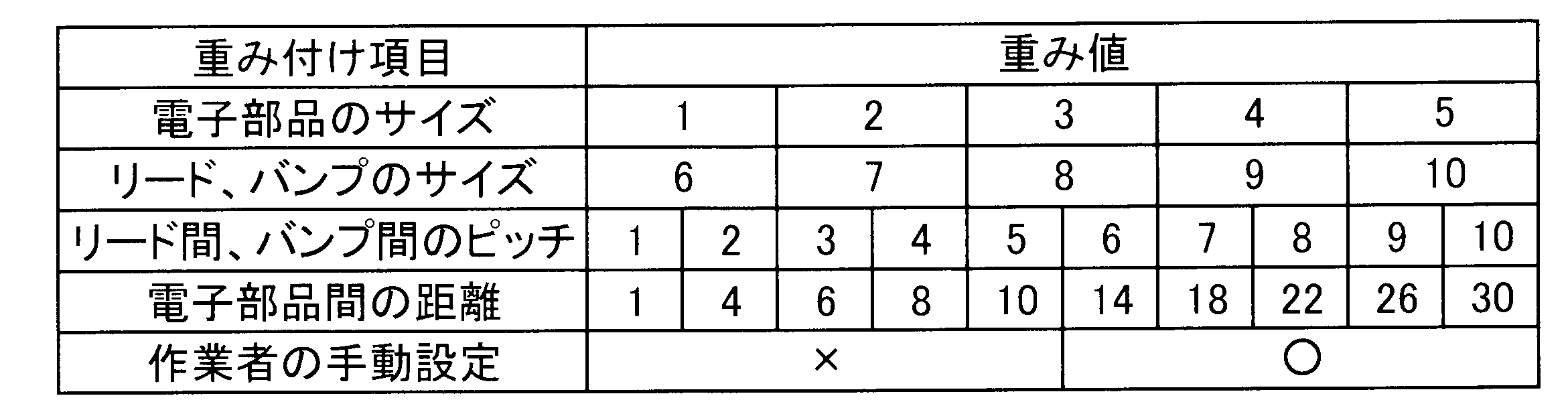
表2に示すように、各項目間で、重み値が異なっていてもよい。また、各項目間で、階級数(分割数)が異なっていてもよい。また、各項目間で、複数の階級間の重み値の増減量は一定でなくてもよい。また、単一の項目内で、複数の階級間の重み値の増減量は一定でなくてもよい。
図12に、電子部品のサイズと重み値との相関図を示す。図12に示す階段状の相関線L1は、表1における項目「電子部品のサイズ」の、重み値の変化に対応している。相関線L1のように、電子部品のサイズの違いに対して、階段状に重み値を変化させてもよい。また、相関線L2のように、電子部品のサイズの違いに対して、直線状に重み値を変化させてもよい。また、相関線L3のように、電子部品のサイズの違いに対して、曲線状に重み値を変化させてもよい。電子部品のサイズが小さくなるのに従って、急激にパッドの印刷状態が悪化する確率が高くなる場合は、相関線L3のような重み付けが有効である。なお、表1に示す「電子部品のサイズ」以外の項目についても、勿論、相関線L1~L3のように、重み付けを行うことができる。
上記実施形態においては、図3に示すように、記憶部71に、形状データ、部品間距離データ、手動設定データ、基板Bに対する全ての検査エリア、表1に示す重み付けテーブル、重み値の総和に対するしきい値を、格納した。しかしながら、図1に示す上位制御装置94、スクリーン印刷機90の制御装置、電子部品実装機91の制御装置、基板外観検査機92の制御装置、リフロー炉の制御装置に、上記各種データを格納してもよい。
図4のステップ1~ステップ5の順序は特に限定しない。ステップ6において、ステップ1~ステップ4の重み値の総和が計算できればよい。
また、表1に示す各項目(図4のステップ1~ステップ5に対応)において、一つでも最大の重み値が出たら(例えば、「リード間、バンプ間のピッチ」(図4のステップ3に対応)の重み値=5の場合)、重み値の総和によらず、当該検査エリアを検査を実行する検査エリアに選定してもよい。また、図1に示す基板外観検査機92として、本発明の基板検査機を具現化してもよい。基板外観検査機92の構成、動きは、第一実施形態のはんだ検査機1(図2、図3)と同様である。
Claims (16)
- 基板に装着される電子部品の形状に関する形状データ、該電子部品と該電子部品に隣り合う別の電子部品との間の距離に関する部品間距離データのうち、少なくとも一つを含む部品関連データを基に、予め該基板に設定される複数の検査エリアに対して、検査の優先度に関する重み付け作業を行う重み付けステップと、
該重み付け作業の結果を基に、複数の該検査エリアから、該検査を実行する該検査エリアを選択する検査エリア選択ステップと、
を有する検査エリア決定方法。 - 前記形状データは、前記電子部品のサイズを含む請求項1に記載の検査エリア決定方法。
- 前記電子部品は、部品本体と、該部品本体と前記基板との間の導通を確保する導通部と、を有し、
前記形状データは、該導通部のサイズを含む請求項1または請求項2に記載の検査エリア決定方法。 - 前記電子部品は、部品本体と、該部品本体と前記基板との間の導通を確保する複数の導通部と、を有し、
前記形状データは、複数の該導通部の間のピッチを含む請求項1ないし請求項3のいずれかに記載の検査エリア決定方法。 - 前記部品関連データは、作業者が手動で設定する手動設定データを含む請求項1ないし請求項4のいずれかに記載の検査エリア決定方法。
- 前記部品関連データには、前記検査の優先度に関する重み値が関連付けられており、
前記検査エリア選択ステップにおいては、該重み値の総和が所定のしきい値を超過する前記検査エリアを、該検査を実行する該検査エリアに選択する請求項1ないし請求項5のいずれかに記載の検査エリア決定方法。 - 前記検査エリア選択ステップにおいては、前記重み付け作業の結果に加えて、前記基板の生産に要するサイクルタイムを基に、前記検査を実行する前記検査エリアを選択する請求項1ないし請求項6のいずれかに記載の検査エリア決定方法。
- 前記検査は、前記基板に対するはんだの印刷状態の検査である請求項1ないし請求項7のいずれかに記載の検査エリア決定方法。
- 基板に装着される電子部品の形状に関する形状データ、該電子部品と該電子部品に隣り合う別の電子部品との間の距離に関する部品間距離データのうち、少なくとも一つを含む部品関連データを基に、予め該基板に設定される複数の検査エリアに対して、検査の優先度に関する重み付け作業を行う重み付けステップと、
該重み付け作業の結果を基に、複数の該検査エリアから、該検査を実行する該検査エリアを選択する検査エリア選択ステップと、
を実行する制御装置と、
選択された該検査エリアに対して検査を実行する検査ヘッドと、
を備え、該基板に対して行われた作業の結果を検査する基板検査機。 - 前記形状データは、前記電子部品のサイズを含む請求項9に記載の基板検査機。
- 前記電子部品は、部品本体と、該部品本体と前記基板との間の導通を確保する導通部と、を有し、
前記形状データは、該導通部のサイズを含む請求項9または請求項10に記載の基板検査機。 - 前記電子部品は、部品本体と、該部品本体と前記基板との間の導通を確保する複数の導通部と、を有し、
前記形状データは、複数の該導通部の間のピッチを含む請求項9ないし請求項11のいずれかに記載の基板検査機。 - 前記部品関連データは、作業者が手動で設定する手動設定データを含む請求項9ないし請求項12のいずれかに記載の基板検査機。
- 前記部品関連データには、前記検査の優先度に関する重み値が関連付けられており、
前記検査エリア選択ステップにおいては、該重み値の総和が所定のしきい値を超過する前記検査エリアを、該検査を実行する該検査エリアに選択する請求項9ないし請求項13のいずれかに記載の基板検査機。 - 前記検査エリア選択ステップにおいては、前記重み付け作業の結果に加えて、前記基板の生産に要するサイクルタイムを基に、前記検査を実行する前記検査エリアを選択する請求項9ないし請求項14のいずれかに記載の基板検査機。
- 前記検査は、前記基板に対するはんだの印刷状態の検査である請求項9ないし請求項15のいずれかに記載の基板検査機。
Priority Applications (2)
| Application Number | Priority Date | Filing Date | Title |
|---|---|---|---|
| PCT/JP2012/069200 WO2014016959A1 (ja) | 2012-07-27 | 2012-07-27 | 検査エリア決定方法および基板検査機 |
| JP2014526689A JP6023198B2 (ja) | 2012-07-27 | 2012-07-27 | 検査エリア決定方法および基板検査機 |
Applications Claiming Priority (1)
| Application Number | Priority Date | Filing Date | Title |
|---|---|---|---|
| PCT/JP2012/069200 WO2014016959A1 (ja) | 2012-07-27 | 2012-07-27 | 検査エリア決定方法および基板検査機 |
Publications (1)
| Publication Number | Publication Date |
|---|---|
| WO2014016959A1 true WO2014016959A1 (ja) | 2014-01-30 |
Family
ID=49996792
Family Applications (1)
| Application Number | Title | Priority Date | Filing Date |
|---|---|---|---|
| PCT/JP2012/069200 Ceased WO2014016959A1 (ja) | 2012-07-27 | 2012-07-27 | 検査エリア決定方法および基板検査機 |
Country Status (2)
| Country | Link |
|---|---|
| JP (1) | JP6023198B2 (ja) |
| WO (1) | WO2014016959A1 (ja) |
Cited By (1)
| Publication number | Priority date | Publication date | Assignee | Title |
|---|---|---|---|---|
| JP2022053087A (ja) * | 2020-09-24 | 2022-04-05 | 株式会社Fuji | 検査支援装置および検査支援方法 |
Citations (4)
| Publication number | Priority date | Publication date | Assignee | Title |
|---|---|---|---|---|
| JPH0862275A (ja) * | 1994-08-24 | 1996-03-08 | Matsushita Electric Ind Co Ltd | 実装検査データ作成方法 |
| JP2009170531A (ja) * | 2008-01-11 | 2009-07-30 | Yamaha Motor Co Ltd | 部品実装装置 |
| JP2010016266A (ja) * | 2008-07-04 | 2010-01-21 | Panasonic Corp | 実装条件決定方法 |
| JP2012044028A (ja) * | 2010-08-20 | 2012-03-01 | Fuji Mach Mfg Co Ltd | 実装基板検査装置及び実装基板検査方法 |
Family Cites Families (1)
| Publication number | Priority date | Publication date | Assignee | Title |
|---|---|---|---|---|
| JP4090705B2 (ja) * | 2001-05-14 | 2008-05-28 | 松下電器産業株式会社 | 実装基板の外観検査システムおよび外観検査方法 |
-
2012
- 2012-07-27 WO PCT/JP2012/069200 patent/WO2014016959A1/ja not_active Ceased
- 2012-07-27 JP JP2014526689A patent/JP6023198B2/ja active Active
Patent Citations (4)
| Publication number | Priority date | Publication date | Assignee | Title |
|---|---|---|---|---|
| JPH0862275A (ja) * | 1994-08-24 | 1996-03-08 | Matsushita Electric Ind Co Ltd | 実装検査データ作成方法 |
| JP2009170531A (ja) * | 2008-01-11 | 2009-07-30 | Yamaha Motor Co Ltd | 部品実装装置 |
| JP2010016266A (ja) * | 2008-07-04 | 2010-01-21 | Panasonic Corp | 実装条件決定方法 |
| JP2012044028A (ja) * | 2010-08-20 | 2012-03-01 | Fuji Mach Mfg Co Ltd | 実装基板検査装置及び実装基板検査方法 |
Cited By (2)
| Publication number | Priority date | Publication date | Assignee | Title |
|---|---|---|---|---|
| JP2022053087A (ja) * | 2020-09-24 | 2022-04-05 | 株式会社Fuji | 検査支援装置および検査支援方法 |
| JP7601589B2 (ja) | 2020-09-24 | 2024-12-17 | 株式会社Fuji | 検査支援装置および検査支援方法 |
Also Published As
| Publication number | Publication date |
|---|---|
| JPWO2014016959A1 (ja) | 2016-07-07 |
| JP6023198B2 (ja) | 2016-11-09 |
Similar Documents
| Publication | Publication Date | Title |
|---|---|---|
| KR101123464B1 (ko) | 부품 실장 방법, 부품 실장기, 실장 조건 결정 방법, 실장 조건 결정 장치 및 프로그램 | |
| US6904672B2 (en) | Method for mounting an electronic component | |
| JP4767995B2 (ja) | 部品実装方法、部品実装機、実装条件決定方法、実装条件決定装置およびプログラム | |
| JP3965288B2 (ja) | 対基板作業結果検査装置 | |
| CN110268220B (zh) | 基板检查装置、基板检查方法以及基板的制造方法 | |
| CN105074439B (zh) | 印刷电路板的印刷检查方法和印刷检查装置 | |
| CN110352635B (zh) | 部件安装系统及粘接剂检查装置 | |
| US20060174480A1 (en) | Inspection method and apparatus for mounted electronic components | |
| CN101106899A (zh) | 部件搭载位置校正方法及部件安装装置 | |
| US20140373346A1 (en) | Electronic component mounting system and electronic component mounting method | |
| JP5781834B2 (ja) | 対基板作業検査支援装置 | |
| WO2018216101A1 (ja) | 装着順序決定装置、装着順序検査装置、装着順序決定方法、および装着順序検査方法 | |
| JP4917071B2 (ja) | ヘッド配置決定方法およびプログラム | |
| JP5739754B2 (ja) | 電子回路部品の立上がり防止方法および電子回路製造システム | |
| JP6023198B2 (ja) | 検査エリア決定方法および基板検査機 | |
| WO2012165261A1 (ja) | はんだマーク設定方法およびはんだマーク設定装置 | |
| JP7466746B2 (ja) | 対策情報案内装置および対策情報案内方法 | |
| JP4263519B2 (ja) | 自動部品マウント装置の検査方法 | |
| US11330751B2 (en) | Board work machine | |
| JP7235603B2 (ja) | 部品実装用データの変更装置、変更プログラム、及び、表面実装機 | |
| JP2011124518A (ja) | 実装基板生産装置、部品実装基板搬送装置及び実装基板生産方法 | |
| WO2020178991A1 (ja) | 補正量算出装置および補正量算出方法 | |
| EP3315903B1 (en) | Board inspection apparatus | |
| JP2013084646A (ja) | 基板処理システム、基板供給順序決定方法、プログラム、記録媒体 | |
| JP7094366B2 (ja) | 検査設定装置および検査設定方法 |
Legal Events
| Date | Code | Title | Description |
|---|---|---|---|
| 121 | Ep: the epo has been informed by wipo that ep was designated in this application |
Ref document number: 12881715 Country of ref document: EP Kind code of ref document: A1 |
|
| ENP | Entry into the national phase |
Ref document number: 2014526689 Country of ref document: JP Kind code of ref document: A |
|
| NENP | Non-entry into the national phase |
Ref country code: DE |
|
| 122 | Ep: pct application non-entry in european phase |
Ref document number: 12881715 Country of ref document: EP Kind code of ref document: A1 |