WO2014013961A1 - 液晶表示装置 - Google Patents
液晶表示装置 Download PDFInfo
- Publication number
- WO2014013961A1 WO2014013961A1 PCT/JP2013/069237 JP2013069237W WO2014013961A1 WO 2014013961 A1 WO2014013961 A1 WO 2014013961A1 JP 2013069237 W JP2013069237 W JP 2013069237W WO 2014013961 A1 WO2014013961 A1 WO 2014013961A1
- Authority
- WO
- WIPO (PCT)
- Prior art keywords
- gate
- bus lines
- liquid crystal
- display device
- crystal display
- Prior art date
- Legal status (The legal status is an assumption and is not a legal conclusion. Google has not performed a legal analysis and makes no representation as to the accuracy of the status listed.)
- Ceased
Links
Images








Classifications
-
- G—PHYSICS
- G02—OPTICS
- G02F—OPTICAL DEVICES OR ARRANGEMENTS FOR THE CONTROL OF LIGHT BY MODIFICATION OF THE OPTICAL PROPERTIES OF THE MEDIA OF THE ELEMENTS INVOLVED THEREIN; NON-LINEAR OPTICS; FREQUENCY-CHANGING OF LIGHT; OPTICAL LOGIC ELEMENTS; OPTICAL ANALOGUE/DIGITAL CONVERTERS
- G02F1/00—Devices or arrangements for the control of the intensity, colour, phase, polarisation or direction of light arriving from an independent light source, e.g. switching, gating or modulating; Non-linear optics
- G02F1/01—Devices or arrangements for the control of the intensity, colour, phase, polarisation or direction of light arriving from an independent light source, e.g. switching, gating or modulating; Non-linear optics for the control of the intensity, phase, polarisation or colour
- G02F1/13—Devices or arrangements for the control of the intensity, colour, phase, polarisation or direction of light arriving from an independent light source, e.g. switching, gating or modulating; Non-linear optics for the control of the intensity, phase, polarisation or colour based on liquid crystals, e.g. single liquid crystal display cells
- G02F1/133—Constructional arrangements; Operation of liquid crystal cells; Circuit arrangements
- G02F1/136—Liquid crystal cells structurally associated with a semi-conducting layer or substrate, e.g. cells forming part of an integrated circuit
- G02F1/1362—Active matrix addressed cells
- G02F1/136286—Wiring, e.g. gate line, drain line
-
- G—PHYSICS
- G02—OPTICS
- G02F—OPTICAL DEVICES OR ARRANGEMENTS FOR THE CONTROL OF LIGHT BY MODIFICATION OF THE OPTICAL PROPERTIES OF THE MEDIA OF THE ELEMENTS INVOLVED THEREIN; NON-LINEAR OPTICS; FREQUENCY-CHANGING OF LIGHT; OPTICAL LOGIC ELEMENTS; OPTICAL ANALOGUE/DIGITAL CONVERTERS
- G02F1/00—Devices or arrangements for the control of the intensity, colour, phase, polarisation or direction of light arriving from an independent light source, e.g. switching, gating or modulating; Non-linear optics
- G02F1/01—Devices or arrangements for the control of the intensity, colour, phase, polarisation or direction of light arriving from an independent light source, e.g. switching, gating or modulating; Non-linear optics for the control of the intensity, phase, polarisation or colour
- G02F1/13—Devices or arrangements for the control of the intensity, colour, phase, polarisation or direction of light arriving from an independent light source, e.g. switching, gating or modulating; Non-linear optics for the control of the intensity, phase, polarisation or colour based on liquid crystals, e.g. single liquid crystal display cells
- G02F1/133—Constructional arrangements; Operation of liquid crystal cells; Circuit arrangements
- G02F1/13306—Circuit arrangements or driving methods for the control of single liquid crystal cells
-
- G—PHYSICS
- G02—OPTICS
- G02F—OPTICAL DEVICES OR ARRANGEMENTS FOR THE CONTROL OF LIGHT BY MODIFICATION OF THE OPTICAL PROPERTIES OF THE MEDIA OF THE ELEMENTS INVOLVED THEREIN; NON-LINEAR OPTICS; FREQUENCY-CHANGING OF LIGHT; OPTICAL LOGIC ELEMENTS; OPTICAL ANALOGUE/DIGITAL CONVERTERS
- G02F1/00—Devices or arrangements for the control of the intensity, colour, phase, polarisation or direction of light arriving from an independent light source, e.g. switching, gating or modulating; Non-linear optics
- G02F1/01—Devices or arrangements for the control of the intensity, colour, phase, polarisation or direction of light arriving from an independent light source, e.g. switching, gating or modulating; Non-linear optics for the control of the intensity, phase, polarisation or colour
- G02F1/13—Devices or arrangements for the control of the intensity, colour, phase, polarisation or direction of light arriving from an independent light source, e.g. switching, gating or modulating; Non-linear optics for the control of the intensity, phase, polarisation or colour based on liquid crystals, e.g. single liquid crystal display cells
- G02F1/133—Constructional arrangements; Operation of liquid crystal cells; Circuit arrangements
- G02F1/136—Liquid crystal cells structurally associated with a semi-conducting layer or substrate, e.g. cells forming part of an integrated circuit
- G02F1/1362—Active matrix addressed cells
- G02F1/136277—Active matrix addressed cells formed on a semiconductor substrate, e.g. of silicon
-
- G—PHYSICS
- G02—OPTICS
- G02F—OPTICAL DEVICES OR ARRANGEMENTS FOR THE CONTROL OF LIGHT BY MODIFICATION OF THE OPTICAL PROPERTIES OF THE MEDIA OF THE ELEMENTS INVOLVED THEREIN; NON-LINEAR OPTICS; FREQUENCY-CHANGING OF LIGHT; OPTICAL LOGIC ELEMENTS; OPTICAL ANALOGUE/DIGITAL CONVERTERS
- G02F1/00—Devices or arrangements for the control of the intensity, colour, phase, polarisation or direction of light arriving from an independent light source, e.g. switching, gating or modulating; Non-linear optics
- G02F1/01—Devices or arrangements for the control of the intensity, colour, phase, polarisation or direction of light arriving from an independent light source, e.g. switching, gating or modulating; Non-linear optics for the control of the intensity, phase, polarisation or colour
- G02F1/13—Devices or arrangements for the control of the intensity, colour, phase, polarisation or direction of light arriving from an independent light source, e.g. switching, gating or modulating; Non-linear optics for the control of the intensity, phase, polarisation or colour based on liquid crystals, e.g. single liquid crystal display cells
- G02F1/133—Constructional arrangements; Operation of liquid crystal cells; Circuit arrangements
- G02F1/136—Liquid crystal cells structurally associated with a semi-conducting layer or substrate, e.g. cells forming part of an integrated circuit
- G02F1/1362—Active matrix addressed cells
- G02F1/1368—Active matrix addressed cells in which the switching element is a three-electrode device
-
- H—ELECTRICITY
- H10—SEMICONDUCTOR DEVICES; ELECTRIC SOLID-STATE DEVICES NOT OTHERWISE PROVIDED FOR
- H10D—INORGANIC ELECTRIC SEMICONDUCTOR DEVICES
- H10D30/00—Field-effect transistors [FET]
- H10D30/60—Insulated-gate field-effect transistors [IGFET]
- H10D30/67—Thin-film transistors [TFT]
- H10D30/6757—Thin-film transistors [TFT] characterised by the structure of the channel, e.g. transverse or longitudinal shape or doping profile
-
- H—ELECTRICITY
- H10—SEMICONDUCTOR DEVICES; ELECTRIC SOLID-STATE DEVICES NOT OTHERWISE PROVIDED FOR
- H10D—INORGANIC ELECTRIC SEMICONDUCTOR DEVICES
- H10D86/00—Integrated devices formed in or on insulating or conducting substrates, e.g. formed in silicon-on-insulator [SOI] substrates or on stainless steel or glass substrates
- H10D86/40—Integrated devices formed in or on insulating or conducting substrates, e.g. formed in silicon-on-insulator [SOI] substrates or on stainless steel or glass substrates characterised by multiple TFTs
- H10D86/421—Integrated devices formed in or on insulating or conducting substrates, e.g. formed in silicon-on-insulator [SOI] substrates or on stainless steel or glass substrates characterised by multiple TFTs having a particular composition, shape or crystalline structure of the active layer
-
- H—ELECTRICITY
- H10—SEMICONDUCTOR DEVICES; ELECTRIC SOLID-STATE DEVICES NOT OTHERWISE PROVIDED FOR
- H10D—INORGANIC ELECTRIC SEMICONDUCTOR DEVICES
- H10D86/00—Integrated devices formed in or on insulating or conducting substrates, e.g. formed in silicon-on-insulator [SOI] substrates or on stainless steel or glass substrates
- H10D86/40—Integrated devices formed in or on insulating or conducting substrates, e.g. formed in silicon-on-insulator [SOI] substrates or on stainless steel or glass substrates characterised by multiple TFTs
- H10D86/60—Integrated devices formed in or on insulating or conducting substrates, e.g. formed in silicon-on-insulator [SOI] substrates or on stainless steel or glass substrates characterised by multiple TFTs wherein the TFTs are in active matrices
Definitions
- the present invention relates to a liquid crystal display device.
- This application claims priority based on Japanese Patent Application No. 2012-160848 filed in Japan on July 19, 2012, the contents of which are incorporated herein by reference.
- liquid crystal display device As a form of liquid crystal display device, a liquid crystal display device driven by an inversion driving method is known.
- the inversion driving method there are various methods such as a frame inversion method, a line inversion method, a column inversion method, and a dot inversion method.
- Patent Document 1 discloses a so-called Z-inversion type liquid crystal display device in which a data line is driven by a column inversion method and a liquid crystal cell is driven by a dot inversion method.
- the liquid crystal display device of Patent Document 1 does not have a configuration that takes into account the misalignment. As a result, when misalignment occurs, there is a problem that the holding characteristics of the thin film transistor are changed and display quality is deteriorated.
- the present invention has been made to solve the above-described problem, and an object of the present invention is to provide a liquid crystal display device capable of suppressing a change in retention characteristics of a thin film transistor and suppressing a deterioration in display quality. To do.
- the present invention employs the following means. (1) That is, the liquid crystal display device according to the first aspect of the present invention is disposed adjacent to each other so as to intersect with the plurality of source bus lines adjacent to each other. A plurality of thin film transistors provided corresponding to each intersection of the plurality of source bus lines and the plurality of gate bus lines, and provided corresponding to each of the plurality of thin film transistors. A plurality of pixel electrodes to which an image signal is supplied from the source bus line via the thin film transistor, and the image signal whose polarity is inverted between a positive potential and a negative potential every unit period. A plurality of pixel electrodes connected to each of the plurality of source bus lines.
- a semiconductor including a source part, a channel part, and a drain part, wherein the plurality of thin film transistors are alternately arranged on one side and the other side in an arrangement direction of the plurality of source bus lines along a line extending direction.
- a gate electrode constituted by a part of the gate bus line, and the source portion, the channel portion, and the drain portion are mutually in a direction intersecting with an arrangement direction of the plurality of source bus lines.
- the gate electrodes are arranged adjacent to each other, extend in a direction parallel to the arrangement direction of the plurality of source bus lines, and are arranged to face the channel portion.
- the semiconductor layer includes a channel region functioning as the channel portion, a high concentration impurity region functioning as the source portion or the drain portion, and the channel.
- a low concentration impurity region provided between the region and the high concentration impurity region,
- the length of the low-concentration impurity region in the extending direction of the source bus line is the length of the plurality of gate bus lines and the plurality of thin film transistors in the arrangement direction of the plurality of source bus lines. It may be invariant to the relative position shift.
- each of the plurality of thin film transistors includes a plurality of gate electrodes configured by a part of the gate bus line along the gate bus line.
- a multi-gate structure may be provided.
- each of the plurality of thin film transistors may have a double gate structure in which two gate electrodes are arranged along the gate bus line.
- each of the plurality of thin film transistors may have a triple gate structure in which three gate electrodes are arranged along the gate bus line.
- each of the plurality of thin film transistors includes one gate electrode formed by a part of the gate bus line along the gate bus line. It may have a single gate structure arranged.
- each of the plurality of thin film transistors has a holding characteristic that the plurality of gate buses in an arrangement direction of the plurality of source bus lines. It may be invariant with respect to a shift in relative position between the line and the plurality of thin film transistors.
- the array of the plurality of pixels may be a stripe array.
- the material for forming the semiconductor layer may include an oxide composed of indium, gallium, and zinc.
- liquid crystal display device capable of suppressing a change in holding characteristics of a thin film transistor and suppressing a decrease in display quality.
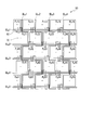
- FIG. 1 is a schematic diagram illustrating a liquid crystal display device according to a first embodiment of the present invention. It is a top view which expands and shows the principal part of the liquid crystal display device which concerns on 1st Embodiment of this invention.
- FIG. 3 is a cross-sectional view taken along line AA in FIG. 2. It is a top view which expands and shows the principal part of the liquid crystal display device which concerns on a comparative example. It is a top view which expands and shows the principal part of the liquid crystal display device which concerns on a comparative example. It is a top view which expands and shows the principal part of the liquid crystal display device which concerns on 1st Embodiment of this invention.
- FIG. 1 is a schematic diagram showing a liquid crystal display device 1 according to the first embodiment of the present invention.
- the liquid crystal display device 1 according to the present embodiment includes a liquid crystal panel 2, a source driver 3, a gate driver 4, and a control device 5.
- the liquid crystal panel 2 includes an element substrate 10.
- the element substrate 10 On the element substrate 10, a plurality of pixels, which are the minimum unit areas for display, are arranged in a matrix.
- the element substrate 10 includes a plurality of source bus lines (SL1 to SLm + 1), a plurality of gate bus lines (GL1 to GLn), a plurality of thin film transistors 6 (Thin Film Transistor, hereinafter abbreviated as TFT), and a plurality of thin film transistors.
- Pixel electrode 7 is provided.
- source bus lines may be collectively referred to as source bus lines SL.
- Gate bus lines may be collectively referred to as gate bus lines GL.
- the plurality of source bus lines (SL1 to SLm + 1) are arranged adjacent to each other so as to extend in parallel to each other.
- the plurality of gate bus lines (GL1 to GLn) extend in parallel to each other and are arranged adjacent to each other so as to be orthogonal to the plurality of source bus lines (SL1 to SLm + 1).
- a plurality of source bus lines (SL1 to SLm + 1) and a plurality of gate bus lines (GL1 to GLn) are formed in a lattice pattern.
- a rectangular area defined by the adjacent source bus line SL and the adjacent gate bus line GL becomes one pixel P.
- a plurality of pixels (P11 to Pnm) are arranged in a matrix.
- the arrangement of a plurality of pixels is a stripe arrangement. Specifically, a plurality of pixels (P11 to Pnm) are arranged in a stripe shape along the extending direction of the source bus line SL.
- the plurality of TFTs 6 are provided corresponding to the intersections of the plurality of source bus lines (SL1 to SLm + 1) and the plurality of gate bus lines (GL1 to GLn).
- the TFT 6 supplies the image signal from the source bus line SL to the pixel electrode 7 in response to the scan signal from the gate bus line GL. Details of the TFT 6 will be described later.
- the plurality of pixel electrodes 7 are provided corresponding to each of the plurality of TFTs 6.
- the plurality of pixel electrodes 7 are connected to each of the plurality of source bus lines (SL1 to SLm + 1).
- the plurality of pixel electrodes 7 connected to one source bus line SL are arranged along the extending direction of the source bus line SL (hereinafter sometimes referred to as the vertical line direction).
- SLm + 1) are arranged alternately on one side (left side shown in FIG. 1) and the other side (right side shown in FIG. 1) of the arrangement direction (hereinafter sometimes referred to as horizontal line direction).
- the odd-numbered pixel electrode 7 connected to the odd-numbered gate bus lines (GL1, GL3, GL5,...) In the vertical line direction has a source bus line (SLi) (here) I is a positive integer).
- the even-numbered pixel electrodes 7 connected to the even-numbered gate bus lines (GL2, GL4, GL6,...) In the vertical line direction are connected to the source bus line (SLi + 1) adjacent to the right side. .
- An image signal is supplied to the plurality of pixel electrodes 7 from the source bus line SL via the TFT 6.
- the pixel electrode 7 drives the liquid crystal positioned between the common electrode (not shown) in response to the image signal. Thereby, the light transmittance is adjusted.
- the control device 5 supplies an image signal to the source driver 3.
- the control device 5 supplies control signals to the gate driver 4 and the source driver 3.
- the control signals supplied to the gate driver 4 include a gate start pulse (GSP), a gate shift clock signal (GSC), and a gate output enable signal (GOE).
- GSP gate start pulse
- GSC gate shift clock signal
- GOE gate output enable signal
- the control signal supplied to the source driver 3 includes a source start pulse (SSP), a source shift clock signal (SSC), a source output enable signal (SOE), a polarity control signal (POL), and the like.
- SSP source start pulse
- SSC source shift clock signal
- SOE source output enable signal
- POL polarity control signal
- the gate driver 4 sequentially supplies scan signals to the gate bus lines (GL1 to GLn) in the order of GL1, GL2, GL3,. In response to this scan signal, the TFT 6 is driven in units of horizontal lines.
- the source driver 3 converts the supplied image signal into an analog image signal.
- the source driver 3 supplies an image signal for one horizontal line to a plurality of source bus lines (SL1 to SLm + 1) every horizontal period in which a scan signal is supplied to the gate bus line GL.
- the source driver 3 supplies the image signal to the column inversion method.
- Image signals supplied to each of the plurality of source bus lines (SL1 to SLm + 1) have opposite polarities in adjacent source bus lines SL. Specifically, the odd-numbered source bus lines (SL1, SL3,%) And the even-numbered source bus lines (SL2, SL4,...) In the horizontal line direction have mutually opposite polarities.
- a signal is supplied.
- the polarities of the image signals supplied to the plurality of source bus lines (SL1 to SLm + 1) are inverted in units of frames under the control of the control device 5.
- an image signal having a positive potential is supplied to odd-numbered source bus lines (SL1, SL3,%) In the horizontal line direction, and even-numbered source bus lines (SL2, SL4,. ⁇ ) shows a state in which an image signal having a negative potential is supplied.
- the source driver 3 supplies an image signal whose polarity is inverted between a positive potential and a negative potential to each of the plurality of source bus lines (SL1 to SLm + 1) for each unit period (one vertical scanning period).
- the liquid crystal display device 1 employs a so-called Z-inversion method in which the pixel electrode 7 is driven by the dot inversion method while the source bus line SL is driven by the column inversion method. ing.
- FIG. 2 is an enlarged plan view showing a main part of the liquid crystal display device 1 according to the present embodiment.
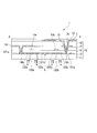
- FIG. 3 is a cross-sectional view taken along line AA in FIG.
- three source bus lines (SL1 to SL3) and three of the regions partitioned into a plurality of source bus lines (SL1 to SLm + 1) and a plurality of gate bus lines (GL1 to GLn) are shown.
- the area partitioned into the gate bus lines (GL1 to GL3) is shown enlarged.
- liquid crystal panel applicable to the present invention is not limited to an active matrix transmissive liquid crystal panel.
- the liquid crystal panel applicable to the present invention may be, for example, a transflective type (transmission / reflection type) liquid crystal panel.
- the liquid crystal panel 2 includes an element substrate 10 (see FIG. 3), a color filter substrate (not shown), and a liquid crystal layer (not shown).
- the liquid crystal panel 2 of the present embodiment performs display in, for example, a TN (Twisted Nematic) mode, and a liquid crystal having a positive dielectric anisotropy is used for the liquid crystal layer.
- TN Transmission Nematic
- the liquid crystal display device 1 of the present invention is not limited to the above TN mode as a display mode, but is a VA (Vertical Alignment, Vertical Alignment) mode, an STN (Super Twisted Nematic) mode, an IPS (In-Plane Switching) mode, an FFS ( (Fringe FieldingSwitching) mode or the like can be used.
- VA Vertical Alignment, Vertical Alignment
- STN Super Twisted Nematic
- IPS In-Plane Switching
- FFS Frringe FieldingSwitching
- a TFT 6 is formed on a transparent substrate 11 constituting the element substrate 10.
- the TFT 6 includes a semiconductor layer 12, a first gate electrode 13a, and a second gate electrode 13b.
- the TFT 6 of this embodiment is an n-channel type.
- the TFT 6 is not limited to the n-channel type but may be a p-channel type.
- a glass substrate can be used as the transparent substrate 11, for example.
- the material for forming the semiconductor layer 12 include CGS (Continuous Grain Silicon: Continuous Grain Boundary Silicon), LPS (Low-temperature Poly-Silicon: Low-temperature polycrystalline silicon), ⁇ -Si (Amorphous Silicon: Amorphous Silicon), and the like.
- a silicon semiconductor can be used.
- the semiconductor layer 12 includes a first channel region 120a, a second channel region 120b, a first high concentration impurity region 121a, a second high concentration impurity region 121b, a third high concentration impurity region 121c, a first low concentration impurity region 122a, 2 includes a low concentration impurity region 122b, a third low concentration impurity region 122c, and a fourth low concentration impurity region 122d.
- the first channel region 120 a and the second channel region 120 b function as a channel portion of the semiconductor layer 12.
- the first high concentration impurity region 121 a functions as a source part of the semiconductor layer 12.
- the second high concentration impurity region 121 b functions as a drain portion of the semiconductor layer 12.
- the first gate electrode 13a and the second gate electrode 13b are constituted by a part of the gate bus line GL.
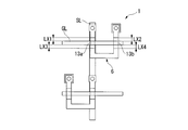
- the TFT 6 has a double gate structure in which the first gate electrode 13a and the second gate electrode 13b are arranged along the gate bus line GL.
- the TFT 6 is formed in a U shape in plan view.
- the first high-concentration impurity region 121a and the first channel region 120a are arranged adjacent to each other with the first low-concentration impurity region 122a interposed therebetween in a direction orthogonal to the horizontal line direction.
- the second high-concentration impurity region 121b and the second channel region 120b are disposed adjacent to each other with the second low-concentration impurity region 122b interposed therebetween in a direction orthogonal to the horizontal line direction.
- the holding characteristics of the plurality of TFTs 6 are invariant with respect to a shift in relative position between the plurality of gate bus lines GL and the plurality of TFTs 6 in the horizontal line direction.
- the “holding characteristic” is stored in the pixel capacitance after a predetermined signal voltage is applied to the pixel electrode 7 and until a new signal voltage is applied to the pixel electrode 7 (one frame period). This is a characteristic of how much charge can be retained.
- the retention characteristics change due to the relative position shift between the gate electrode and the semiconductor layer.
- the retention characteristics in the present embodiment change depending on the relative position shift between the gate electrode, the channel region, and the low concentration impurity region. In the present embodiment, even if the gate bus line GL is displaced in the horizontal line direction, the relative position between the gate electrode and the semiconductor layer is not displaced, so that the holding characteristics of the TFT 6 do not change.
- the first gate electrode 13a extends in a direction parallel to the horizontal line direction.
- the first channel region 120a is disposed below the first gate electrode 13a so as to face the first gate electrode 13a.
- the first channel region 120a is formed in the semiconductor layer 12 in a self-aligned manner with respect to the first gate electrode 13a.
- the first channel region 120a is doped with a p-type impurity such as B (boron).
- the second gate electrode 13b extends in a direction parallel to the horizontal line direction.
- the second channel region 120b is disposed below the second gate electrode 13b so as to face the second gate electrode 13b.
- the second channel region 120b is formed in the semiconductor layer 12 in a self-aligned manner with respect to the second gate electrode 13b.
- the second channel region 120b is doped with a p-type impurity similar to the first channel region 120a.
- the first high-concentration impurity region 121a and the second high-concentration impurity region 121b are provided at an interval so as to sandwich the first channel region 120a and the second channel region 120b.
- the first high-concentration impurity region 121a is provided closer to the source electrode 14 than the first channel region 120a.
- the second high concentration impurity region 121b is provided closer to the drain electrode 15 than the second channel region 120b.
- the third high concentration impurity region 121c is provided between the first channel region 120a and the second channel region 120b.
- the first high-concentration impurity region 121a, the second high-concentration impurity region 121b, and the third high-concentration impurity region 121c each contain n-type impurities at a higher concentration than the low-concentration impurity region. Therefore, in the first high concentration impurity region 121a, the second high concentration impurity region 121b, and the third high concentration impurity region 121c, the n-type carrier concentration is higher than that in the low concentration impurity region.
- the first low-concentration impurity region 122a is provided between the first channel region 120a and the first high-concentration impurity region 121a.
- the second low concentration impurity region 122b is provided between the second channel region 120b and the second high concentration impurity region 121b.
- the third low concentration impurity region 122c is provided between the first channel region 120a and the third high concentration impurity region 121c.
- the fourth low concentration impurity region 122d is provided between the second channel region 120b and the third high concentration impurity region 121c.
- the n-type impurity has a lower concentration than the high-concentration impurity region, respectively. include. Therefore, in the first low concentration impurity region 122a, the second low concentration impurity region 122b, the third low concentration impurity region 122c, and the fourth low concentration impurity region 122d, the n-type carrier concentration is higher than that of the high concentration impurity region. Low.
- 122c, and the third high-concentration impurity region 121c and the fourth low-concentration impurity region 122d each form an LDD (Lightly Doped Drain) structure.
- a gate insulating film 16 is formed on the transparent substrate 11 so as to cover the semiconductor layer 12.
- a material for forming the gate insulating film 16 for example, a silicon oxide film, a silicon nitride film, or a laminated film thereof can be used.
- the length of the first low-concentration impurity region 122a in the vertical line direction is defined as a first length L1.
- the length of the second low-concentration impurity region 122b in the vertical line direction is defined as a second length L2.
- the length of the third low-concentration impurity region 122c in the vertical line direction is a third length L3.
- the length of the fourth low-concentration impurity region 122d in the vertical line direction is set to a fourth length L4.
- the first length L1 and the third length L3 are invariant with respect to the relative positional shift between the plurality of gate bus lines GL and the plurality of TFTs 6 in the horizontal line direction.
- the second length L ⁇ b> 2 and the fourth length L ⁇ b> 4 are invariant with respect to the relative position shift between the plurality of gate bus lines GL and the plurality of TFTs 6 in the horizontal line direction.
- a first gate electrode 13 a is formed at a position facing the first channel region 120 a of the semiconductor layer 12.
- a second gate electrode 13 b is formed at a position facing the second channel region 120 b of the semiconductor layer 12.
- a material for forming the first gate electrode 13a and the second gate electrode 13b for example, a laminated film of W (tungsten) / TaN (tantalum nitride), Mo (molybdenum), Ti (titanium), Al (aluminum), or the like is used. Can do.
- a first interlayer insulating film 17 is formed on the gate insulating film 16 so as to cover the first gate electrode 13a and the second gate electrode 13b.
- a material for forming the first interlayer insulating film 17 for example, a silicon oxide film, a silicon nitride film, or a laminated film thereof can be used.
- a source electrode 14 and a drain electrode 15 are formed on the first interlayer insulating film 17.
- the source electrode 14 is connected to the first high-concentration impurity region 121 a of the semiconductor layer 12 through a contact hole 14 h that penetrates the first interlayer insulating film 17 and the gate insulating film 16.
- the drain electrode 15 is connected to the second high-concentration impurity region 121 b of the semiconductor layer 12 through a contact hole 15 h that penetrates the first interlayer insulating film 17 and the gate insulating film 16.
- the same conductive material as that of the gate electrode 13 described above can be used.
- a second interlayer insulating film 18 is formed on the first interlayer insulating film 17 so as to cover the source electrode 14 and the drain electrode 15.
- a forming material of the second interlayer insulating film 18 a forming material similar to the first interlayer insulating film 17 described above or an organic insulating material can be used.
- a pixel electrode 7 is formed on the second interlayer insulating film 18.
- the pixel electrode 7 is connected to the drain electrode 15 through a contact hole 7 h that penetrates the second interlayer insulating film 18.
- the pixel electrode 7 is connected to the second high-concentration impurity region 121b of the semiconductor layer 12 using the drain electrode 15 as a relay electrode.
- a transparent conductive material such as ITO (Indium Tin Oxide, Indium Tin Oxide), IZO (Indium Zinc Oxide, Indium Zinc Oxide) can be used.
- An alignment film 19 is formed on the second interlayer insulating film 18 so as to cover the pixel electrode 7.
- the alignment film 19 has an alignment regulating force that horizontally aligns the liquid crystal molecules constituting the liquid crystal layer.
- the form of the TFT 6 may be a top gate type TFT or a bottom gate type TFT.
- 4A to 5B are schematic diagrams for explaining the operation of the arrangement configuration of the TFTs 6 in the liquid crystal display device 1 according to the present embodiment.
- FIG. 4A and FIG. 4B are plan views showing an enlarged main part of a liquid crystal display device 1X according to a comparative example.
- FIG. 4A is a diagram before a relative position shift between the plurality of gate bus lines and the plurality of TFTs in the horizontal line direction, that is, a so-called alignment shift.
- FIG. 4B is a diagram after an alignment shift occurs in the horizontal line direction.
- reference characters LX1, LX2, LX3, and LX4 denote the length (first length) and second low length of the first low-concentration impurity region in the vertical line direction before the misalignment in the horizontal line direction occurs, respectively.
- the length of the concentration impurity region in the vertical line direction (second length), the length of the third low concentration impurity region in the horizontal line direction (third length), and the length of the fourth low concentration impurity region in the horizontal line direction This is the length (fourth length).
- symbols LX1 ′, LX2 ′, LX3 ′, and LX4 ′ are respectively the first length, the second length, the third length, and the first length after the occurrence of misalignment in the horizontal line direction. 4 lengths.
- FIG. 5A and FIG. 5B are plan views showing enlarged main parts of the liquid crystal display device 1 according to the present embodiment.
- FIG. 5A is a diagram before an alignment shift occurs in the horizontal line direction.
- FIG. 5B is a diagram after an alignment shift occurs in the horizontal line direction.
- reference numerals L1, L2, L3, and L4 denote a first length, a second length, a third length, and a fourth length, respectively, before alignment displacement occurs in the horizontal line direction. is there.
- reference numerals L1 ′, L2 ′, L3 ′, and L4 ′ respectively denote the first length, the second length, the third length, and the first length after the occurrence of misalignment in the horizontal line direction. 4 lengths.
- the TFT 6X of the liquid crystal display device 1X according to the comparative example includes a first gate electrode 13Xa and a second gate electrode 13Xb.
- the first gate electrode 13Xa and the second gate electrode 13Xb are each configured by a part of the gate bus line GLX.
- the TFT 6X has a double gate structure in which the first gate electrode 13Xa and the second gate electrode 13Xb are arranged along the gate bus line GLX.
- the TFT 6X is formed in an L shape in plan view.
- the first gate electrode 13Xa extends in a direction parallel to the horizontal line direction.
- the second gate electrode 13Xb extends in a direction orthogonal to the horizontal line direction.
- a part of the gate bus line GLX protrudes upward in parallel with the extending direction of the source bus line SLX.
- the second gate electrode 13Xb is configured by a part of the protruding portion of the source bus line SLX.
- the second length LX2 'after the alignment deviation in the horizontal line direction is shorter than the second length LX2 before the alignment deviation in the horizontal line direction occurs (LX2' ⁇ LX2).
- the fourth length LX4 'after the alignment deviation in the horizontal line direction is longer than the fourth length LX4 before the alignment deviation in the horizontal line direction occurs (LX4'> LX4).
- the holding characteristics of the TFT 6X change before and after the occurrence of misalignment in the horizontal line direction, the holding characteristics of the TFT 6X change, resulting in display quality. Will cause a decline.
- the holding characteristics of the TFT 6X change as shown in FIG. 6A, a grayscale difference is generated for each horizontal line in the display image, and uneven stripes are recognized.
- L1 L1 ′
- L2 L2 ′
- L3 L3 ′
- L4 L4 ′
- the Z-inversion method since the Z-inversion method is adopted, power consumption can be reduced as compared with the dot inversion method.
- the polarity array applied to the pixel In the Z-inversion method, the polarity array applied to the pixel is in a dot inversion state. For this reason, it is possible to suppress the occurrence of crosstalk between pixels and to suppress the occurrence of flicker.
- the source part, the channel part, and the drain part of the semiconductor layer are arranged in the vertical line direction, and the gate electrode extends in a direction parallel to the horizontal line direction. For this reason, even when an alignment shift occurs in the horizontal line direction, it is possible to suppress a change in the holding characteristics of the TFT 6 and suppress a deterioration in display quality.
- the present invention is not limited to this.
- the present invention can be applied even when the TFT has a multi-gate structure such as a triple gate structure or a quattro gate structure.
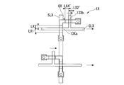
- FIG. 7 is an enlarged plan view showing a main part of the liquid crystal display device 1A according to the present embodiment.
- the TFT 6 has a double gate structure and is formed in a U shape in a plan view.
- the TFT 6A of the present embodiment has a triple gate structure and is formed in an S shape in plan view.
- the TFT 6A includes a first gate electrode 13Aa, a second gate electrode 13Ab, and a third gate electrode 13Ac.
- the first gate electrode 13Aa, the second gate electrode 13Ab, and the third gate electrode 13Ac each extend in a direction parallel to the horizontal line direction.
- the TFT 6A has a triple gate structure in which a first gate electrode 13Aa, a second gate electrode 13Ab, and a third gate electrode 13Ac are arranged along the gate bus line GL.
- the codes LA1, LA2, LA3, LA4, LA5, LA6 are respectively the first length, the second length, the third length, the fourth length, the fifth length, 6 lengths.
- the sixth length LA6 is invariable.
- the liquid crystal display device 1A even in the case of misalignment in the horizontal line direction in the triple gate structure TFT 6A, the change in the holding characteristics of the TFT 6A is suppressed, and the deterioration in display quality is suppressed. can do.
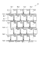
- FIG. 8 is an enlarged plan view showing a main part of the liquid crystal display device 1B according to the present embodiment.
- the arrangement of the plurality of pixels is a stripe arrangement.
- the arrangement of the plurality of pixels (P D 11 to P D 55) is a delta arrangement. Specifically, the pixel arrangement positions are shifted by a half pixel between the odd-numbered pixels and the even-numbered pixels.
- the center position of the second pixel P D 32 from the row end (left end) of the third row is 1 pixel in the row direction of the second pixel P D 22 from the row end of the second row ( It is shifted to the left by half of the width in the horizontal direction.
- the center position of the third row of the row end second pixel P D 32 is 1 second from the second central position and the fifth row of the row end of the pixel P D 12 from row in edge pixel P D 52 matches the center position in the row direction.
- the center position of the second pixel P D 22 from the end of the second row coincides with the center position of the second pixel P D 42 from the end of the fourth row in the row direction.
- the source bus line SL D is a plan view zigzag.
- the pixel electrode 7B is a square in plan view.
- the odd-numbered pixel electrodes 7B connected to the odd-numbered gate bus lines (GL D 1, GL D 3, GL D 5,...) In the vertical line direction are connected to the source bus adjacent to the right side.
- Line (SL D i + 1) (where i is a positive integer).
- even-numbered gate bus lines (GL D 2, GL4, ⁇ ) in the vertical line direction even-numbered pixel electrodes 7B connected to is connected to a source bus line adjacent to the left (SL D i) ing.
- the liquid crystal display device 1B even if the pixel arrangement is a delta arrangement and an alignment shift occurs in the horizontal line direction in the TFT 6B having a double gate structure, the change in the holding characteristics of the TFT 6B is changed. Can be suppressed, and deterioration of display quality can be suppressed.
- FIG. 9 is an enlarged plan view showing a main part of the liquid crystal display device 1C according to the present embodiment.
- four source bus lines (SL D 1 to SL D m + 1) and four source bus lines (GL D 1 to GL D n) are divided into a plurality of gate bus lines (GL D 1 to GL D n).
- the liquid crystal display device 1C even if the pixel arrangement is a delta arrangement and the alignment deviation in the horizontal line direction occurs in the triple gate structure TFT 6C, the change in the holding characteristics of the TFT 6C is changed. Can be suppressed, and deterioration of display quality can be suppressed.
- FIG. 10 is an enlarged plan view showing a main part of the liquid crystal display device 1D according to the present embodiment.
- the TFT 6 has a double gate structure and is formed in a U shape in a plan view.
- the TFT 6D of the present embodiment has a single gate structure and is formed in an L shape in plan view.
- TFT 6D includes one gate electrode 13D.
- the gate electrode 13D extends in a direction parallel to the horizontal line direction.
- the TFT 6D has a single gate structure in which one gate electrode 13D is arranged along the gate bus line GL.
- symbols LD1 and LD2 have a first length and a second length, respectively.
- the first length LD1 and the second length LD2 are unchanged before and after an alignment shift in the horizontal line direction occurs.
- liquid crystal display device 1D even when the alignment deviation in the horizontal line direction occurs in the single-gate TFT 6D, the change in the holding characteristics of the TFT 6D is suppressed, and the deterioration in display quality is suppressed. can do.
- the sixth embodiment of the present invention will be described below.
- the basic configuration of the liquid crystal display device according to this embodiment is the same as that of the first embodiment, and IGZO (In—Ga—Zn—) is an oxide composed of indium, gallium, and zinc as a material for forming a semiconductor layer.
- IGZO In—Ga—Zn—
- O-based semiconductor O-based semiconductor
- the oxide semiconductor has higher mobility than ⁇ -Si. Therefore, a TFT using an oxide semiconductor can operate at a higher speed than a TFT using ⁇ -Si.
- the oxide semiconductor film is formed by a simpler process than the polycrystalline silicon film, the oxide semiconductor film can be applied to a device that requires a large area.
- the oxide semiconductor layer can be formed as follows, for example. First, an IGZO film having a thickness of 30 nm to 300 nm is formed on the insulating film by sputtering. Next, a resist mask that covers a predetermined region of the IGZO film is formed by photolithography. Next, the portion of the IGZO film that is not covered with the resist mask is removed by wet etching. Thereafter, the resist mask is peeled off. In this manner, an oxide semiconductor layer is obtained.
- IZO In—Zn—O-based semiconductor
- ZTO an oxide composed of zinc and titanium
- Zn—Ti—O based semiconductor Zn—Ti—O based semiconductor
- the present invention can be used for a liquid crystal display device.
- second high concentration impurity region (drain portion), GL, GL D ... Gate bus line, SL, SL D ... Source bus line, L1... First length (length of first low-concentration impurity region in vertical line direction), L2... Second length (first 2 length of the low concentration impurity region in the vertical line direction), L3... Third length (length of the third low concentration impurity region in the vertical line direction), L4... Fourth length (fourth low concentration impurity) Length of the region in the vertical line direction), L5 ... fifth length, L6 ... sixth length
Landscapes
- Physics & Mathematics (AREA)
- Nonlinear Science (AREA)
- Mathematical Physics (AREA)
- Chemical & Material Sciences (AREA)
- Crystallography & Structural Chemistry (AREA)
- General Physics & Mathematics (AREA)
- Optics & Photonics (AREA)
- Engineering & Computer Science (AREA)
- Microelectronics & Electronic Packaging (AREA)
- Liquid Crystal (AREA)
- Devices For Indicating Variable Information By Combining Individual Elements (AREA)
Abstract
この液晶表示装置において、複数のソースバスラインの各々に接続される複数の画素電極は、ソースバスラインの延在方向に沿って、複数のソースバスラインの並び方向の一方側及び他方側に交互に配置され、薄膜トランジスタは、ソース部とチャネル部とドレイン部とを含む半導体層と、ゲートバスラインの一部によって構成されるゲート電極と、を含み、ソース部とチャネル部とドレイン部とは、複数のソースバスラインの並び方向と交差する方向に互いに隣接して配置され、ゲート電極は、複数のソースバスラインの並び方向と平行な方向に延在し、チャネル部と対向して配置されている。
Description
本発明は、液晶表示装置に関する。
本願は、2012年7月19日に、日本に出願された特願2012-160848号に基づき優先権を主張し、その内容をここに援用する。
本願は、2012年7月19日に、日本に出願された特願2012-160848号に基づき優先権を主張し、その内容をここに援用する。
液晶表示装置の一形態として、インバージョン駆動方式で駆動する液晶表示装置が知られている。インバージョン駆動方式としては、フレーム・インバージョン方式、ライン・インバージョン方式、コラム・インバージョン方式、ドット・インバージョン方式等の種々の方式がある。
例えば、特許文献1には、データラインをコラム・インバージョン方式で駆動するとともに液晶セルをドット・インバージョン方式で駆動する、いわゆるZ-インバージョン方式の液晶表示装置が開示されている。
ところで、液晶表示装置を製造する際、データラインやゲートライン等の配線層と薄膜トランジスタとの相対位置のずれ、いわゆるアライメントずれが生じることがある。しかしながら、特許文献1の液晶表示装置では、アライメントずれを考慮した構成となっていない。その結果、アライメントずれが生じた場合、薄膜トランジスタの保持特性が変化し、表示品位が低下するという問題があった。
本発明は、上記の課題を解決するためになされたものであって、薄膜トランジスタの保持特性の変化を抑制し、表示品位の低下を抑制することが可能な液晶表示装置を提供することを目的とする。
上記の目的を達成するために、本発明は以下の手段を採用した。
(1)すなわち、本発明の第一の態様に係る液晶表示装置は、互いに隣接して配置された複数のソースバスラインと、前記複数のソースバスラインと交差するように互いに隣接して配置された複数のゲートバスラインと、前記複数のソースバスラインと前記複数のゲートバスラインとの各交差部に対応して設けられた複数の薄膜トランジスタと、前記複数の薄膜トランジスタの各々に対応して設けられ、前記薄膜トランジスタを介して前記ソースバスラインから画像信号が供給される複数の画素電極と、単位期間毎に正極性電位と負極性電位とに極性が反転する前記画像信号を前記複数のソースバスラインの各々に供給するソースドライバーと、を含み、前記複数のソースバスラインの各々に接続される複数の前記画素電極は、前記ソースバスラインの延在方向に沿って、前記複数のソースバスラインの並び方向の一方側及び他方側に交互に配置され、前記複数の薄膜トランジスタの各々は、ソース部とチャネル部とドレイン部とを含む半導体層と、前記ゲートバスラインの一部によって構成されるゲート電極と、を含み、前記ソース部と前記チャネル部と前記ドレイン部とは、前記複数のソースバスラインの並び方向と交差する方向に互いに隣接して配置され、前記ゲート電極は、前記複数のソースバスラインの並び方向と平行な方向に延在し、前記チャネル部と対向して配置されている。
(1)すなわち、本発明の第一の態様に係る液晶表示装置は、互いに隣接して配置された複数のソースバスラインと、前記複数のソースバスラインと交差するように互いに隣接して配置された複数のゲートバスラインと、前記複数のソースバスラインと前記複数のゲートバスラインとの各交差部に対応して設けられた複数の薄膜トランジスタと、前記複数の薄膜トランジスタの各々に対応して設けられ、前記薄膜トランジスタを介して前記ソースバスラインから画像信号が供給される複数の画素電極と、単位期間毎に正極性電位と負極性電位とに極性が反転する前記画像信号を前記複数のソースバスラインの各々に供給するソースドライバーと、を含み、前記複数のソースバスラインの各々に接続される複数の前記画素電極は、前記ソースバスラインの延在方向に沿って、前記複数のソースバスラインの並び方向の一方側及び他方側に交互に配置され、前記複数の薄膜トランジスタの各々は、ソース部とチャネル部とドレイン部とを含む半導体層と、前記ゲートバスラインの一部によって構成されるゲート電極と、を含み、前記ソース部と前記チャネル部と前記ドレイン部とは、前記複数のソースバスラインの並び方向と交差する方向に互いに隣接して配置され、前記ゲート電極は、前記複数のソースバスラインの並び方向と平行な方向に延在し、前記チャネル部と対向して配置されている。
(2)本発明の第二の態様に係る液晶表示装置は、前記半導体層は、前記チャネル部として機能するチャネル領域と、前記ソース部または前記ドレイン部として機能する高濃度不純物領域と、前記チャネル領域と前記高濃度不純物領域との間に設けられた低濃度不純物領域と、を含み、
前記複数の薄膜トランジスタの各々において、前記ソースバスラインの延在方向における前記低濃度不純物領域の長さは、前記複数のソースバスラインの並び方向における前記複数のゲートバスラインと前記複数の薄膜トランジスタとの相対位置のずれに対して不変であってもよい。
前記複数の薄膜トランジスタの各々において、前記ソースバスラインの延在方向における前記低濃度不純物領域の長さは、前記複数のソースバスラインの並び方向における前記複数のゲートバスラインと前記複数の薄膜トランジスタとの相対位置のずれに対して不変であってもよい。
(3)上記(1)または(2)に記載の液晶表示装置では、前記複数の薄膜トランジスタの各々は、前記ゲートバスラインの一部によって構成されるゲート電極が前記ゲートバスラインに沿って複数配置されたマルチゲート構造を有してもよい。
(4)上記(3)に記載の液晶表示装置では、前記複数の薄膜トランジスタの各々は、前記ゲート電極が前記ゲートバスラインに沿って二つ配置されたダブルゲート構造を有してもよい。
(5)上記(3)に記載の液晶表示装置では、前記複数の薄膜トランジスタの各々は、前記ゲート電極が前記ゲートバスラインに沿って三つ配置されたトリプルゲート構造を有してもよい。
(6)上記(1)または(2)に記載の液晶表示装置では、前記複数の薄膜トランジスタの各々は、前記ゲートバスラインの一部によって構成されるゲート電極が前記ゲートバスラインに沿って一つ配置されたシングルゲート構造を有してもよい。
(7)上記(1)ないし(6)のいずれか一項に記載の液晶表示装置では、前記複数の薄膜トランジスタの各々の保持特性は、前記複数のソースバスラインの並び方向における前記複数のゲートバスラインと前記複数の薄膜トランジスタとの相対位置のずれに対して不変であってもよい。
(8)上記(1)ないし(7)のいずれか一項に記載の液晶表示装置では、隣接する前記ソースバスラインと隣接する前記ゲートバスラインとによって区画された領域を一つの画素としたとき、複数の前記画素の配列がストライプ配列であってもよい。
(9)上記(1)ないし(7)のいずれか一項に記載の液晶表示装置では、隣接する前記ソースバスラインと隣接する前記ゲートバスラインとによって区画された領域を一つの画素としたとき、複数の前記画素の配列がデルタ配列であってもよい。
(10)上記(1)ないし(9)のいずれか一項に記載の液晶表示装置では、前記半導体層の形成材料が、インジウム、ガリウム、及び亜鉛から構成される酸化物を含んでもよい。
本発明によれば、薄膜トランジスタの保持特性の変化を抑制し、表示品位の低下を抑制することが可能な液晶表示装置を提供することができる。
[第1実施形態]
以下、本発明の第1実施形態について、図1~図6Bを用いて説明する。
なお、以下の全ての図面においては、各構成要素を見やすくするため、構成要素によって寸法の縮尺を異ならせて示すことがある。
以下、本発明の第1実施形態について、図1~図6Bを用いて説明する。
なお、以下の全ての図面においては、各構成要素を見やすくするため、構成要素によって寸法の縮尺を異ならせて示すことがある。
図1は、本発明の第1実施形態に係る液晶表示装置1を示す模式図である。
図1に示すように、本実施形態に係る液晶表示装置1は、液晶パネル2と、ソースドライバー3と、ゲートドライバー4と、制御装置5と、を備えている。液晶パネル2は、素子基板10を含んでいる。
図1に示すように、本実施形態に係る液晶表示装置1は、液晶パネル2と、ソースドライバー3と、ゲートドライバー4と、制御装置5と、を備えている。液晶パネル2は、素子基板10を含んでいる。
素子基板10には、表示の最小単位領域である画素がマトリクス状に複数配置されている。素子基板10には、複数のソースバスライン(SL1~SLm+1)と、複数のゲートバスライン(GL1~GLn)と、複数の薄膜トランジスタ6(Thin Film Transistor,以下、TFTと略記する)と、複数の画素電極7と、が設けられている。以下の説明においては、ソースバスラインを総称してソースバスラインSLと記載することがある。ゲートバスラインを総称してゲートバスラインGLと記載することがある。
複数のソースバスライン(SL1~SLm+1)は、互いに平行に延在するように隣接して配置されている。複数のゲートバスライン(GL1~GLn)は、互いに平行に延在し、かつ、複数のソースバスライン(SL1~SLm+1)と直交するように互いに隣接して配置されている。素子基板10上には、複数のソースバスライン(SL1~SLm+1)と複数のゲートバスライン(GL1~GLn)とが格子状に形成されている。隣接するソースバスラインSLと隣接するゲートバスラインGLとによって区画された矩形状の領域が一つの画素Pとなる。本実施形態では、複数の画素(P11~Pnm)がマトリクス状に配置されている。
また、本実施形態では、複数の画素(P11~Pnm)の配列がストライプ配列である。具体的には、複数の画素(P11~Pnm)がソースバスラインSLの延在方向に沿ってストライプ状に配列されている。
複数のTFT6は、複数のソースバスライン(SL1~SLm+1)と複数のゲートバスライン(GL1~GLn)との各交差部に対応して設けられている。TFT6は、ゲートバスラインGLからのスキャン信号に応答してソースバスラインSLからの画像信号を画素電極7に供給する。TFT6の詳細については後述する。
複数の画素電極7は、複数のTFT6の各々に対応して設けられている。複数の画素電極7は、複数のソースバスライン(SL1~SLm+1)の各々に接続されている。一本のソースバスラインSLに接続される複数の画素電極7は、ソースバスラインSLの延在方向(以下、垂直ライン方向と称することがある)に沿って、複数のソースバスライン(SL1~SLm+1)の並び方向(以下、水平ライン方向と称することがある)の一方側(図1に示す左側)及び他方側(図1に示す右側)に交互に配置されている。
本実施形態では、垂直ライン方向における奇数番目のゲートバスライン(GL1、GL3、GL5、・・・)に接続された奇数番目の画素電極7は、左側に隣接したソースバスライン(SLi) (ここで、iは正の整数)に接続されている。一方、垂直ライン方向における偶数番目のゲートバスライン(GL2、GL4、GL6 、・・・)に接続された偶数番目の画素電極7は、右側に隣接したソースバスライン(SLi+1)に接続されている。
複数の画素電極7には、TFT6を介してソースバスラインSLから画像信号が供給される。画素電極7は、画像信号に応答して共通電極(図示略)との間に位置する液晶を駆動する。これにより、光の透過率が調節される。
制御装置5は、ソースドライバー3に画像信号を供給する。制御装置5は、ゲートドライバー4及びソースドライバー3に制御信号を供給する。
ゲートドライバー4に供給される制御信号には、ゲート・スタートパルス(GSP)、ゲート・シフト・クロック信号(GSC)、ゲート出力イネーブル信号(GOE)が含まれる。
ソースドライバー3に供給される制御信号には、ソース・スタートパルス(SSP)、ソース・シフト・クロック信号(SSC)、ソース出力イネーブル信号(SOE)、極性制御信号(POL)等が含まれる。
ゲートドライバー4は、GL1、GL2、GL3、・・・GLnの順に、ゲートバスライン(GL1~GLn)にスキャン信号を順次的に供給する。このスキャン信号に応答して、TFT6が水平ライン単位で駆動される。
ソースドライバー3は、供給された画像信号をアナログ画像信号に変換する。ソースドライバー3は、ゲートバスラインGLにスキャン信号が供給される1水平期間ごとに、1水平ライン分の画像信号を複数のソースバスライン(SL1~SLm+1)に供給する。
ソースドライバー3は、コラム・インバージョン方式に画像信号を供給する。複数のソースバスライン(SL1~SLm+1)のそれぞれに供給される画像信号は、互いに隣接するソースバスラインSLにおいて相反する極性を有する。具体的には、水平ライン方向における奇数番目のソースバスライン(SL1、SL3、・・・)と偶数番目のソースバスライン(SL2、SL4、・・・)とには、互いに相反する極性の画像信号が供給される。複数のソースバスライン(SL1~SLm+1)に供給される画像信号の極性は、制御装置5の制御により、1フレーム単位で反転される。
図1では、水平ライン方向における奇数番目のソースバスライン(SL1、SL3、・・・)に正極性電位の画像信号が供給され、水平ライン方向における偶数番目のソースバスライン(SL2、SL4、・・・)に負極性電位の画像信号が供給された状態を示している。ソースドライバー3は、単位期間(1垂直走査期間)毎に、正極性電位と負極性電位とに極性が反転する画像信号を複数のソースバスライン(SL1~SLm+1)の各々に供給する。
このように本実施形態に係る液晶表示装置1は、ソースバスラインSLをコラム・インバージョン方式に駆動しながら画素電極7をドット・インバージョン方式で駆動する、いわゆるZ-インバージョン方式を採用している。
以下、液晶パネル2の具体的な構成について説明する。
図2は、本実施形態に係る液晶表示装置1の要部を拡大して示す平面図である。
図3は、図2のA-A線に沿った断面図である。図2においては、複数のソースバスライン(SL1~SLm+1)と複数のゲートバスライン(GL1~GLn)とに区画された領域のうち、3本のソースバスライン(SL1~SL3)と3本のゲートバスライン(GL1~GL3)とに区画された領域を拡大して示している。
図2は、本実施形態に係る液晶表示装置1の要部を拡大して示す平面図である。
図3は、図2のA-A線に沿った断面図である。図2においては、複数のソースバスライン(SL1~SLm+1)と複数のゲートバスライン(GL1~GLn)とに区画された領域のうち、3本のソースバスライン(SL1~SL3)と3本のゲートバスライン(GL1~GL3)とに区画された領域を拡大して示している。
ここでは、アクティブマトリクス方式の透過型液晶パネルを一例に挙げて説明するが、本発明に適用可能な液晶パネルはアクティブマトリクス方式の透過型液晶パネルに限るものではない。本発明に適用可能な液晶パネルは、例えば半透過型(透過・反射兼用型)液晶パネルであっても良い。
液晶パネル2は、素子基板10(図3参照)と、カラーフィルター基板(図示略)と、液晶層(図示略)と、を備えている。本実施形態の液晶パネル2は、例えばTN(Twisted Nematic)モードで表示を行うものであり、液晶層には誘電率異方性が正の液晶が用いられる。
本発明の液晶表示装置1は、表示モードとして、上記のTNモードに限らず、VA(Vertical Alignment,垂直配向)モード、STN(Super Twisted Nematic)モード、IPS(In-Plane Switching)モード、FFS(Fringe Field Switching)モード等を用いることができる。ただし、本実施形態では、TNモードの液晶パネル2を用いた例を挙げる。
図3に示すように、素子基板10を構成する透明基板11上には、TFT6が形成されている。TFT6は、半導体層12と、第1ゲート電極13aと、第2ゲート電極13bと、を備えている。本実施形態のTFT6はnチャネル型である。TFT6は、nチャネル型に限らず、pチャネル型であってもよい。
透明基板11としては、例えばガラス基板を用いることができる。半導体層12の形成材料としては、例えばCGS(Continuous Grain Silicon:連続粒界シリコン)、LPS(Low-temperature Poly-Silicon:低温多結晶シリコン)、α-Si(Amorphous Silicon:非結晶シリコン)等のシリコン半導体を用いることができる。
半導体層12は、第1チャネル領域120a、第2チャネル領域120b、第1高濃度不純物領域121a、第2高濃度不純物領域121b、第3高濃度不純物領域121c、第1低濃度不純物領域122a、第2低濃度不純物領域122b、第3低濃度不純物領域122c、及び第4低濃度不純物領域122dを含んでいる。
第1チャネル領域120a、第2チャネル領域120bは、半導体層12のチャネル部として機能する。第1高濃度不純物領域121aは、半導体層12のソース部として機能する。第2高濃度不純物領域121bは、半導体層12のドレイン部として機能する。
図2に示すように、第1ゲート電極13a、第2ゲート電極13bは、ゲートバスラインGLの一部によって構成されている。TFT6は、第1ゲート電極13a、第2ゲート電極13bがゲートバスラインGLに沿って配置されたダブルゲート構造を有する。TFT6は、平面視U字型に形成されている。
図2及び図3に示すように、第1高濃度不純物領域121aと第1チャネル領域120aとは、水平ライン方向と直交する方向に、第1低濃度不純物領域122aを挟んで互いに隣接して配置されている。第2高濃度不純物領域121bと第2チャネル領域120bとは、水平ライン方向と直交する方向に、第2低濃度不純物領域122bを挟んで互いに隣接して配置されている。
そのため、複数のTFT6の保持特性は、水平ライン方向における複数のゲートバスラインGLと複数のTFT6との相対位置のずれに対して不変である。
ここで、「保持特性」とは、画素電極7に所定の信号電圧を印加した後、この画素電極7に新たな信号電圧を印加するまでの間(1フレーム期間)に、画素容量に蓄えられた電荷をどれだけ保持できるかの特性である。
保持特性は、ゲート電極と半導体層との相対位置のずれによって変化する。本実施形態における保持特性は、ゲート電極とチャネル領域及び低濃度不純物領域との相対位置のずれによって変化する。本実施形態では、ゲートバスラインGLが水平ライン方向にずれても、ゲート電極と半導体層との相対位置にずれが生じないので、TFT6の保持特性は変化しない。
図2に示すように、第1ゲート電極13aは、水平ライン方向と平行な方向に延在している。図3に示すように、第1チャネル領域120aは、第1ゲート電極13aの下方に、第1ゲート電極13aと対向して配置されている。第1チャネル領域120aは、第1ゲート電極13aに対して自己整合的に半導体層12内に形成される。第1チャネル領域120aには、B(ボロン)等のp型不純物がドープされている。
図2に示すように、第2ゲート電極13bは、水平ライン方向と平行な方向に延在している。図3に示すように、第2チャネル領域120bは、第2ゲート電極13bの下方に、第2ゲート電極13bと対向して配置されている。第2チャネル領域120bは、第2ゲート電極13bに対して自己整合的に半導体層12内に形成される。第2チャネル領域120bには、第1チャネル領域120aと同様のp型不純物がドープされている。
第1高濃度不純物領域121a及び第2高濃度不純物領域121bは、第1チャネル領域120a及び第2チャネル領域120bを挟むように間隔を空けて設けられている。第1高濃度不純物領域121aは、第1チャネル領域120aよりもソース電極14側に設けられている。第2高濃度不純物領域121bは、第2チャネル領域120bよりもドレイン電極15側に設けられている。第3高濃度不純物領域121cは、第1チャネル領域120aと第2チャネル領域120bとの間に設けられている。
第1高濃度不純物領域121a、第2高濃度不純物領域121b、及び第3高濃度不純物領域121cには、それぞれn型不純物が低濃度不純物領域に比べて高濃度で含まれている。このため、第1高濃度不純物領域121a、第2高濃度不純物領域121b、及び第3高濃度不純物領域121cにおいては、n型のキャリア濃度が低濃度不純物領域に比べて高い。
第1低濃度不純物領域122aは、第1チャネル領域120aと第1高濃度不純物領域121aとの間に設けられている。第2低濃度不純物領域122bは、第2チャネル領域120bと第2高濃度不純物領域121bとの間に設けられている。第3低濃度不純物領域122cは、第1チャネル領域120aと第3高濃度不純物領域121cとの間に設けられている。第4低濃度不純物領域122dは、第2チャネル領域120bと第3高濃度不純物領域121cとの間に設けられている。
第1低濃度不純物領域122a、第2低濃度不純物領域122b、第3低濃度不純物領域122c、及び第4低濃度不純物領域122dには、それぞれn型不純物が高濃度不純物領域に比べて低濃度で含まれている。このため、第1低濃度不純物領域122a、第2低濃度不純物領域122b、第3低濃度不純物領域122c、及び第4低濃度不純物領域122dにおいては、n型のキャリア濃度が高濃度不純物領域に比べて低い。
このように、第1高濃度不純物領域121a及び第1低濃度不純物領域122a、第2高濃度不純物領域121b及び第2低濃度不純物領域122b、第3高濃度不純物領域121c及び第3低濃度不純物領域122c、並びに第3高濃度不純物領域121c及び第4低濃度不純物領域122dは、それぞれLDD(Lightly Doped Drain)構造を形成している。
透明基板11上には、半導体層12を覆うようにゲート絶縁膜16が形成されている。
ゲート絶縁膜16の形成材料としては、例えばシリコン酸化膜、シリコン窒化膜、もしくはこれらの積層膜等を用いることができる。
ゲート絶縁膜16の形成材料としては、例えばシリコン酸化膜、シリコン窒化膜、もしくはこれらの積層膜等を用いることができる。
図2及び図3において、第1低濃度不純物領域122aの垂直ライン方向の長さを第1の長さL1とする。第2低濃度不純物領域122bの垂直ライン方向の長さを第2の長さL2とする。第3低濃度不純物領域122cの垂直ライン方向の長さを第3の長さL3とする。第4低濃度不純物領域122dの垂直ライン方向の長さを第4の長さL4とする。
第1の長さL1と第3の長さL3とは、水平ライン方向における複数のゲートバスラインGLと複数のTFT6との相対位置のずれに対して不変である。第2の長さL2と第4の長さL4とは、水平ライン方向における複数のゲートバスラインGLと複数のTFT6との相対位置のずれに対して不変である。
ゲート絶縁膜16上には、半導体層12の第1チャネル領域120aと対向する位置に第1ゲート電極13aが形成されている。半導体層12の第2チャネル領域120bと対向する位置に第2ゲート電極13bが形成されている。第1ゲート電極13a及び第2ゲート電極13bの形成材料としては、例えばW(タングステン)/TaN(窒化タンタル)の積層膜、Mo(モリブデン)、Ti(チタン)、Al(アルミニウム)等を用いることができる。
ゲート絶縁膜16上には、第1ゲート電極13a及び第2ゲート電極13bを覆うように第1層間絶縁膜17が形成されている。第1層間絶縁膜17の形成材料としては、例えばシリコン酸化膜、シリコン窒化膜、もしくはこれらの積層膜等を用いることができる。
第1層間絶縁膜17上には、ソース電極14およびドレイン電極15が形成されている。ソース電極14は、第1層間絶縁膜17とゲート絶縁膜16とを貫通するコンタクトホール14hを介して半導体層12の第1高濃度不純物領域121aに接続されている。ドレイン電極15は、第1層間絶縁膜17とゲート絶縁膜16とを貫通するコンタクトホール15hを介して半導体層12の第2高濃度不純物領域121bに接続されている。ソース電極14およびドレイン電極15の形成材料としては、上述のゲート電極13と同様の導電性材料を用いることができる。
第1層間絶縁膜17上には、ソース電極14およびドレイン電極15を覆うように第2層間絶縁膜18が形成されている。第2層間絶縁膜18の形成材料としては、上述の第1層間絶縁膜17と同様の形成材料、もしくは有機絶縁性材料を用いることができる。
第2層間絶縁膜18上には、画素電極7が形成されている。画素電極7は、第2層間絶縁膜18を貫通するコンタクトホール7hを介してドレイン電極15に接続されている。
画素電極7は、ドレイン電極15を中継用電極として半導体層12の第2高濃度不純物領域121bに接続されている。
画素電極7は、ドレイン電極15を中継用電極として半導体層12の第2高濃度不純物領域121bに接続されている。
画素電極7の形成材料としては、例えばITO(Indium Tin Oxide、インジウム錫酸化物)、IZO(Indium Zinc Oxide、インジウム亜鉛酸化物)等の透明導電性材料を用いることができる。
このような構成により、ゲートバスラインGLを通じて走査信号が供給され、TFT6がオン状態となったときに、ソースバスラインSLを通じてソース電極14に供給された画像信号が、半導体層12、ドレイン電極15を経て画素電極7に供給される。
第2層間絶縁膜18上には、画素電極7を覆うように配向膜19が形成されている。配向膜19は、液晶層を構成する液晶分子を水平配向させる配向規制力を有している。なお、TFT6の形態としては、トップゲート型TFTであっても良いし、ボトムゲート型TFTであっても良い。
図4A~図5Bは、本実施形態に係る液晶表示装置1におけるTFT6の配置構成の作用を説明するための模式図である。
図4A及び図4Bは、比較例に係る液晶表示装置1Xの要部を拡大して示す平面図である。図4Aは、水平ライン方向における複数のゲートバスラインと複数のTFTとの相対位置のずれ、いわゆるアライメントずれが生じる前の図である。図4Bは、水平ライン方向におけるアライメントずれが生じた後の図である。
図4Aにおいて、符号LX1,LX2,LX3,LX4は、それぞれ水平ライン方向におけるアライメントずれが生じる前の、第1低濃度不純物領域の垂直ライン方向の長さ(第1の長さ)、第2低濃度不純物領域の垂直ライン方向の長さ(第2の長さ)、第3低濃度不純物領域の水平ライン方向の長さ(第3の長さ)、第4低濃度不純物領域の水平ライン方向の長さ(第4の長さ)である。
図4Bにおいて、符号LX1’,LX2’,LX3’,LX4’は、それぞれ水平ライン方向におけるアライメントずれが生じた後の、第1の長さ、第2の長さ、第3の長さ、第4の長さである。
図4Bにおいて、符号LX1’,LX2’,LX3’,LX4’は、それぞれ水平ライン方向におけるアライメントずれが生じた後の、第1の長さ、第2の長さ、第3の長さ、第4の長さである。
図5A及び図5Bは、本実施形態に係る液晶表示装置1の要部を拡大して示す平面図である。図5Aは、水平ライン方向におけるアライメントずれが生じる前の図である。図5Bは、水平ライン方向におけるアライメントずれが生じた後の図である。
図5Aにおいて、符号L1,L2,L3,L4は、それぞれ水平ライン方向におけるアライメントずれが生じる前の、第1の長さ、第2の長さ、第3の長さ、第4の長さである。
図5Bにおいて、符号L1’,L2’,L3’,L4’は、それぞれ水平ライン方向におけるアライメントずれが生じた後の、第1の長さ、第2の長さ、第3の長さ、第4の長さである。
図5Bにおいて、符号L1’,L2’,L3’,L4’は、それぞれ水平ライン方向におけるアライメントずれが生じた後の、第1の長さ、第2の長さ、第3の長さ、第4の長さである。
図4Aに示すように、比較例に係る液晶表示装置1XのTFT6Xは、第1ゲート電極13Xaと、第2ゲート電極13Xbとを有する。第1ゲート電極13Xa、第2ゲート電極13Xbは、それぞれゲートバスラインGLXの一部によって構成されている。
TFT6Xは、第1ゲート電極13Xa、第2ゲート電極13XbがゲートバスラインGLXに沿って配置されたダブルゲート構造を有する。TFT6Xは、平面視L字型に形成されている。
TFT6Xは、第1ゲート電極13Xa、第2ゲート電極13XbがゲートバスラインGLXに沿って配置されたダブルゲート構造を有する。TFT6Xは、平面視L字型に形成されている。
第1ゲート電極13Xaは、水平ライン方向と平行な方向に延在している。第2ゲート電極13Xbは、水平ライン方向と直交する方向に延在している。ゲートバスラインGLXの一部は、ソースバスラインSLXの延在方向と平行に、上方に向けて突出している。
第2ゲート電極13Xbは、ソースバスラインSLXの突出部分の一部によって構成されている。
第2ゲート電極13Xbは、ソースバスラインSLXの突出部分の一部によって構成されている。
液晶表示装置1Xにおいて水平ライン方向におけるアライメントずれが生じた場合を考える。図4A及び図4Bに示すように、水平ライン方向におけるアライメントずれが生じる前後において、第1の長さLX1,LX1’及び第3の長さLX3,LX3’はそれぞれ不変である(LX1=LX1’、LX3=LX3’)。
一方、水平ライン方向におけるアライメントずれが生じた後の第2の長さLX2’は、水平ライン方向におけるアライメントずれが生じる前の第2の長さLX2よりも短くなる(LX2’<LX2)。水平ライン方向におけるアライメントずれが生じた後の第4の長さLX4’は、水平ライン方向におけるアライメントずれが生じる前の第4の長さLX4よりも長くなる(LX4’>LX4)。
このように、水平ライン方向におけるアライメントずれが生じる前後において、第2の長さLX2,LX2’及び第4の長さLX4,LX4’が変化すると、TFT6Xの保持特性が変化してしまい、表示品位の低下を引き起こすこととなる。TFT6Xの保持特性が変化すると、図6Aに示すように、表示画像において1水平ライン毎に濃淡の差が生じ、スジムラが認識されるようになる。
これに対し、本実施形態では、図5A及び図5Bに示すように、水平ライン方向におけるアライメントずれが生じる前後において、第1の長さL1,L1’、第2の長さL2,L2’、第3の長さL3,L3’、及び第4の長さL4,L4’はそれぞれ不変である(L1=L1’、L2=L2’、L3=L3’、L4=L4’)。このため、水平ライン方向におけるアライメントずれが生じる前後において、TFT6の保持特性が不変となり、表示品位の低下を抑制することができる。TFT6の保持特性が不変であると、図6Bに示すように、表示画像において1水平ライン毎に濃淡の差が生じることが抑制され、スジムラが認識されることが抑制される。
以上のような液晶表示装置1によれば、Z-インバージョン方式を採用しているため、ドット・インバージョン方式に比べて、消費電力を低減できる。Z-インバージョン方式では、画素に与えられる極性の配列がドット反転状態となる。このため、画素間にクロストークが生じることを抑制でき、フリッカの発生を抑制できる。
Z-インバージョン方式では、水平ライン方向のアライメントずれによって、ソースバスラインSLの右側と左側に接続される画素の間に保持特性のばらつきが生じやすい。しかしながら、本実施形態では、半導体層のソース部とチャネル部とドレイン部を垂直ライン方向に配置し、ゲート電極を水平ライン方向と平行な方向に延在させている。そのため、水平ライン方向におけるアライメントずれが生じた場合であっても、TFT6の保持特性の変化を抑制し、表示品位の低下を抑制することができる。
なお、本実施形態では、TFTがダブルゲート構造を有する例を挙げて説明したが、これに限らない。例えば、TFTがトリプルゲート構造やクアトロゲート構造等のマルチゲート構造を有する場合においても本発明を適用可能である。
[第2実施形態]
以下、本発明の第2実施形態について、図7を用いて説明する。
本実施形態に係る液晶表示装置1Aの基本構成は第1実施形態と同一であり、TFT6Aがトリプルゲート構造を有する点が第1実施形態と異なる。したがって、本実施形態では、液晶表示装置1Aの基本構成の説明は省略し、TFT6Aの構造について説明する。
図7は、本実施形態に係る液晶表示装置1Aの要部を拡大して示す平面図である。図7においては、複数のソースバスライン(SL1~SLm+1)と複数のゲートバスライン(GL1~GLn)とに区画された領域のうち、3本のソースバスライン(SL1~SL3)と3本のゲートバスライン(GL1~GL3)とに区画された領域を拡大して示している。
図7において、第1実施形態で用いた図面と共通の構成要素には同一の符号を付し、その詳細な説明は省略する。
以下、本発明の第2実施形態について、図7を用いて説明する。
本実施形態に係る液晶表示装置1Aの基本構成は第1実施形態と同一であり、TFT6Aがトリプルゲート構造を有する点が第1実施形態と異なる。したがって、本実施形態では、液晶表示装置1Aの基本構成の説明は省略し、TFT6Aの構造について説明する。
図7は、本実施形態に係る液晶表示装置1Aの要部を拡大して示す平面図である。図7においては、複数のソースバスライン(SL1~SLm+1)と複数のゲートバスライン(GL1~GLn)とに区画された領域のうち、3本のソースバスライン(SL1~SL3)と3本のゲートバスライン(GL1~GL3)とに区画された領域を拡大して示している。
図7において、第1実施形態で用いた図面と共通の構成要素には同一の符号を付し、その詳細な説明は省略する。
第1実施形態では、TFT6は、ダブルゲート構造を有しており、平面視U字型に形成されていた。これに対して、本実施形態のTFT6Aは、トリプルゲート構造を有しており、平面視S字型に形成されている。
TFT6Aは、第1ゲート電極13Aa、第2ゲート電極13Ab、及び第3ゲート電極13Acを含んでいる。第1ゲート電極13Aa、第2ゲート電極13Ab、及び第3ゲート電極13Acは、それぞれ水平ライン方向と平行な方向に延在している。TFT6Aは、第1ゲート電極13Aa、第2ゲート電極13Ab、及び第3ゲート電極13AcがゲートバスラインGLに沿って配置されたトリプルゲート構造を有する。
図7において、符号LA1,LA2,LA3,LA4,LA5,LA6は、それぞれ第1の長さ、第2の長さ、第3の長さ、第4の長さ、第5の長さ、第6の長さである。
本実施形態では、水平ライン方向におけるアライメントずれが生じる前後において、第1の長さLA1、第2の長さLA2、第3の長さLA3、第4の長さLA4、第5の長さLA5、第6の長さLA6はそれぞれ不変である。
本実施形態に係る液晶表示装置1Aによれば、トリプルゲート構造のTFT6Aにおいて水平ライン方向におけるアライメントずれが生じた場合であっても、TFT6Aの保持特性の変化を抑制し、表示品位の低下を抑制することができる。
[第3実施形態]
以下、本発明の第3実施形態について、図8を用いて説明する。
本実施形態に係る液晶表示装置1Bの基本構成は第1実施形態と同一であり、画素配列がデルタ配列である点が第1実施形態と異なる。したがって、本実施形態では、液晶表示装置1Bの基本構成の説明は省略し、デルタ配列について説明する。
図8は、本実施形態に係る液晶表示装置1Bの要部を拡大して示す平面図である。図8においては、複数のソースバスライン(SLD1~SLDm+1)と複数のゲートバスライン(GLD1~GLDn)とに区画された領域のうち、4本のソースバスライン(SLD1~SLD4)と5本のゲートバスライン(GLD1~GLD5)とに区画された領域を拡大して示している。
図8において、第1実施形態で用いた図面と共通の構成要素には同一の符号を付し、その詳細な説明は省略する。
以下、本発明の第3実施形態について、図8を用いて説明する。
本実施形態に係る液晶表示装置1Bの基本構成は第1実施形態と同一であり、画素配列がデルタ配列である点が第1実施形態と異なる。したがって、本実施形態では、液晶表示装置1Bの基本構成の説明は省略し、デルタ配列について説明する。
図8は、本実施形態に係る液晶表示装置1Bの要部を拡大して示す平面図である。図8においては、複数のソースバスライン(SLD1~SLDm+1)と複数のゲートバスライン(GLD1~GLDn)とに区画された領域のうち、4本のソースバスライン(SLD1~SLD4)と5本のゲートバスライン(GLD1~GLD5)とに区画された領域を拡大して示している。
図8において、第1実施形態で用いた図面と共通の構成要素には同一の符号を付し、その詳細な説明は省略する。
第1実施形態では、複数の画素の配列がストライプ配列であった。これに対して、本実施形態では、図8に示すように、複数の画素(PD11~PD55)の配列がデルタ配列である。具体的には、奇数行の画素と偶数行の画素とでは、画素の配置位置が半画素分ずれている。例えば、3行目の行端(左端)から2番目の画素PD32の中心位置は、2行目の行端から2番目の画素PD22の中心位置に対して1画素の行方向(左右方向)の幅の半分だけ左側にずれている。3行目の行端から2番目の画素PD32の中心位置は、1行目の行端から2番目の画素PD12の中心位置及び5行目の行端から2番目の画素PD52の中心位置と行方向において一致している。2行目の行端から2番目の画素PD22の中心位置は、4行目の行端から2番目の画素PD42の中心位置と行方向において一致している。
本実施形態では、ソースバスラインSLDは平面視ジグザグ形状である。画素電極7Bは平面視正方形である。
本実施形態では、垂直ライン方向における奇数番目のゲートバスライン(GLD1、GLD3、GLD5、・・・)に接続された奇数番目の画素電極7Bは、右側に隣接したソースバスライン(SLDi+1) (ここで、iは正の整数)に接続されている。一方、垂直ライン方向における偶数番目のゲートバスライン(GLD2、GL4、・・・)に接続された偶数番目の画素電極7Bは、左側に隣接したソースバスライン(SLDi)に接続されている。
本実施形態に係る液晶表示装置1Bによれば、画素配列がデルタ配列であり、かつ、ダブルゲート構造のTFT6Bにおいて水平ライン方向におけるアライメントずれが生じた場合であっても、TFT6Bの保持特性の変化を抑制し、表示品位の低下を抑制することができる。
[第4実施形態]
以下、本発明の第4実施形態について、図9を用いて説明する。
本実施形態に係る液晶表示装置1Cの基本構成は第3実施形態と同一であり、TFT6Cがトリプルゲート構造を有する点が第3実施形態と異なる。したがって、本実施形態では、液晶表示装置1Cの基本構成の説明は省略する。
図9は、本実施形態に係る液晶表示装置1Cの要部を拡大して示す平面図である。図9においては、複数のソースバスライン(SLD1~SLDm+1)と複数のゲートバスライン(GLD1~GLDn)とに区画された領域のうち、4本のソースバスライン(SLD1~SLD4)と5本のゲートバスライン(GLD1~GLD5)とに区画された領域を拡大して示している。
図9において、第3実施形態で用いた図面と共通の構成要素には同一の符号を付し、その詳細な説明は省略する。
以下、本発明の第4実施形態について、図9を用いて説明する。
本実施形態に係る液晶表示装置1Cの基本構成は第3実施形態と同一であり、TFT6Cがトリプルゲート構造を有する点が第3実施形態と異なる。したがって、本実施形態では、液晶表示装置1Cの基本構成の説明は省略する。
図9は、本実施形態に係る液晶表示装置1Cの要部を拡大して示す平面図である。図9においては、複数のソースバスライン(SLD1~SLDm+1)と複数のゲートバスライン(GLD1~GLDn)とに区画された領域のうち、4本のソースバスライン(SLD1~SLD4)と5本のゲートバスライン(GLD1~GLD5)とに区画された領域を拡大して示している。
図9において、第3実施形態で用いた図面と共通の構成要素には同一の符号を付し、その詳細な説明は省略する。
本実施形態に係る液晶表示装置1Cによれば、画素配列がデルタ配列であり、かつ、トリプルゲート構造のTFT6Cにおいて水平ライン方向におけるアライメントずれが生じた場合であっても、TFT6Cの保持特性の変化を抑制し、表示品位の低下を抑制することができる。
[第5実施形態]
以下、本発明の第5実施形態について、図10を用いて説明する。
本実施形態に係る液晶表示装置1Dの基本構成は第1実施形態と同一であり、TFT6Dがシングルゲート構造を有する点が第1実施形態と異なる。したがって、本実施形態では、液晶表示装置1Dの基本構成の説明は省略し、TFT6Dの構造について説明する。
図10は、本実施形態に係る液晶表示装置1Dの要部を拡大して示す平面図である。図10においては、複数のソースバスライン(SL1~SLm+1)と複数のゲートバスライン(GL1~GLn)とに区画された領域のうち、3本のソースバスライン(SL1~SL3)と3本のゲートバスライン(GL1~GL3)とに区画された領域を拡大して示している。
図10において、第1実施形態で用いた図面と共通の構成要素には同一の符号を付し、その詳細な説明は省略する。
以下、本発明の第5実施形態について、図10を用いて説明する。
本実施形態に係る液晶表示装置1Dの基本構成は第1実施形態と同一であり、TFT6Dがシングルゲート構造を有する点が第1実施形態と異なる。したがって、本実施形態では、液晶表示装置1Dの基本構成の説明は省略し、TFT6Dの構造について説明する。
図10は、本実施形態に係る液晶表示装置1Dの要部を拡大して示す平面図である。図10においては、複数のソースバスライン(SL1~SLm+1)と複数のゲートバスライン(GL1~GLn)とに区画された領域のうち、3本のソースバスライン(SL1~SL3)と3本のゲートバスライン(GL1~GL3)とに区画された領域を拡大して示している。
図10において、第1実施形態で用いた図面と共通の構成要素には同一の符号を付し、その詳細な説明は省略する。
第1実施形態では、TFT6は、ダブルゲート構造を有しており、平面視U字型に形成されていた。これに対して、本実施形態のTFT6Dは、シングルゲート構造を有しており、平面視L字型に形成されている。
TFT6Dは、1つのゲート電極13Dを含んでいる。ゲート電極13Dは、水平ライン方向と平行な方向に延在している。TFT6Dは、ゲート電極13DがゲートバスラインGLに沿って一つ配置されたシングルゲート構造を有する。
図10において、符号LD1,LD2は、それぞれ第1の長さ、第2の長さである。
本実施形態では、水平ライン方向におけるアライメントずれが生じる前後において、第1の長さLD1、第2の長さLD2はそれぞれ不変である。
本実施形態に係る液晶表示装置1Dによれば、シングルゲート構造のTFT6Dにおいて水平ライン方向におけるアライメントずれが生じた場合であっても、TFT6Dの保持特性の変化を抑制し、表示品位の低下を抑制することができる。
[第6実施形態]
以下、本発明の第6実施形態について説明する。
本実施形態に係る液晶表示装置の基本構成は第1実施形態と同一であり、半導体層の形成材料として、インジウム、ガリウム、及び亜鉛から構成される酸化物であるIGZO(In-Ga-Zn-O系半導体)を用いる点が第1実施形態と異なる。したがって、本実施形態では、液晶表示装置の基本構成の説明は省略し、半導体層の形成材料について説明する。
以下、本発明の第6実施形態について説明する。
本実施形態に係る液晶表示装置の基本構成は第1実施形態と同一であり、半導体層の形成材料として、インジウム、ガリウム、及び亜鉛から構成される酸化物であるIGZO(In-Ga-Zn-O系半導体)を用いる点が第1実施形態と異なる。したがって、本実施形態では、液晶表示装置の基本構成の説明は省略し、半導体層の形成材料について説明する。
第1実施形態では、半導体層12の形成材料として、シリコン半導体を用いる例を説明していた。これに対し、本実施形態では、半導体層の形成材料として、IGZO等の酸化物半導体を用いる例を説明する。酸化物半導体は、α-Siよりも高い移動度を有している。このため、酸化物半導体を用いたTFTは、α-Siを用いたTFTよりも高速で動作することが可能である。また、酸化物半導体膜は、多結晶シリコン膜よりも簡便なプロセスで形成されるため、大面積が必要とされる装置にも適用できる。
酸化物半導体層は、例えば、以下のようにして形成できる。まず、スパッタ法を用いて、厚さが30nm以上300nm以下のIGZO膜を絶縁膜の上に形成する。次いで、フォトリソグラフィにより、IGZO膜の所定の領域を覆うレジストマスクを形成する。次いで、IGZO膜のうちレジストマスクで覆われていない部分をウエットエッチングにより除去する。その後、レジストマスクを剥離する。このようにして、酸化物半導体層が得られる。
なお、酸化物半導体としては、IGZOの他にも、例えばインジウム及び亜鉛から構成される酸化物であるIZO(In-Zn-O系半導体)、亜鉛及びチタンから構成される酸化物であるZTO(Zn-Ti-O系半導体)を用いることができる。
以上、図面を参照しながら本発明に係る好適な実施形態について説明したが、本発明は上記の実施形態に限定されないことは言うまでもない。上記の実施形態において示した各構成部材の諸形状や組み合わせ等は一例であって、本発明の主旨から逸脱しない範囲において設計要求等に基づき種々変更可能である。
その他、液晶表示装置の各構成要素の形状、数、配置、材料、形成方法等に関する具体的な記載は、上記の実施形態に限定されることなく、適宜変更が可能である。
その他、液晶表示装置の各構成要素の形状、数、配置、材料、形成方法等に関する具体的な記載は、上記の実施形態に限定されることなく、適宜変更が可能である。
本発明は、液晶表示装置に利用可能である。
1,1A,1B,1C,1D…液晶表示装置、3…ソースドライバー、4…ゲートドライバー、6,6A,6B,6C,6D…TFT(薄膜トランジスタ)、7,7A,7B,7C,7D…画素電極、12…半導体層、13a…第1ゲート電極、13b…第2ゲート電極、13Aa…第1ゲート電極、13Ab…第2ゲート電極、13Ac…第3ゲート電極、13D…ゲート電極、120a…第1チャネル領域(チャネル部)、120b…第2チャネル領域(チャネル部)、121a…第1高濃度不純物領域(ソース部)、121b…第2高濃度不純物領域(ドレイン部)、GL,GLD…ゲートバスライン、SL,SLD…ソースバスライン、L1…第1の長さ(第1低濃度不純物領域の垂直ライン方向の長さ)、L2…第2の長さ(第2低濃度不純物領域の垂直ライン方向の長さ)、L3…第3の長さ(第3低濃度不純物領域の垂直ライン方向の長さ)、L4…第4の長さ(第4低濃度不純物領域の垂直ライン方向の長さ)、L5…第5の長さ、L6…第6の長さ
Claims (10)
- 互いに隣接して配置された複数のソースバスラインと、
前記複数のソースバスラインと交差するように互いに隣接して配置された複数のゲートバスラインと、
前記複数のソースバスラインと前記複数のゲートバスラインとの各交差部に対応して設けられた複数の薄膜トランジスタと、
前記複数の薄膜トランジスタの各々に対応して設けられ、前記薄膜トランジスタを介して前記ソースバスラインから画像信号が供給される複数の画素電極と、
単位期間毎に正極性電位と負極性電位とに極性が反転する前記画像信号を前記複数のソースバスラインの各々に供給するソースドライバーと、を含み、
前記複数のソースバスラインの各々に接続される複数の前記画素電極は、前記ソースバスラインの延在方向に沿って、前記複数のソースバスラインの並び方向の一方側及び他方側に交互に配置され、
前記複数の薄膜トランジスタの各々は、ソース部とチャネル部とドレイン部とを含む半導体層と、前記ゲートバスラインの一部によって構成されるゲート電極と、を含み、
前記ソース部と前記チャネル部と前記ドレイン部とは、前記複数のソースバスラインの並び方向と交差する方向に互いに隣接して配置され、
前記ゲート電極は、前記複数のソースバスラインの並び方向と平行な方向に延在し、前記チャネル部と対向して配置されている液晶表示装置。 - 前記半導体層は、前記チャネル部として機能するチャネル領域と、前記ソース部または前記ドレイン部として機能する高濃度不純物領域と、前記チャネル領域と前記高濃度不純物領域との間に設けられた低濃度不純物領域と、を含み、
前記複数の薄膜トランジスタの各々において、前記ソースバスラインの延在方向における前記低濃度不純物領域の長さは、前記複数のソースバスラインの並び方向における前記複数のゲートバスラインと前記複数の薄膜トランジスタとの相対位置のずれに対して不変である請求項1に記載の液晶表示装置。 - 前記複数の薄膜トランジスタの各々は、前記ゲートバスラインの一部によって構成されるゲート電極が前記ゲートバスラインに沿って複数配置されたマルチゲート構造を有する請求項1または2に記載の液晶表示装置。
- 前記複数の薄膜トランジスタの各々は、前記ゲート電極が前記ゲートバスラインに沿って二つ配置されたダブルゲート構造を有する請求項3に記載の液晶表示装置。
- 前記複数の薄膜トランジスタの各々は、前記ゲート電極が前記ゲートバスラインに沿って三つ配置されたトリプルゲート構造を有する請求項3に記載の液晶表示装置。
- 前記複数の薄膜トランジスタの各々は、前記ゲートバスラインの一部によって構成されるゲート電極が前記ゲートバスラインに沿って一つ配置されたシングルゲート構造を有する請求項1または2に記載の液晶表示装置。
- 前記複数の薄膜トランジスタの各々の保持特性は、前記複数のソースバスラインの並び方向における前記複数のゲートバスラインと前記複数の薄膜トランジスタとの相対位置のずれに対して不変である請求項1ないし6のいずれか一項に記載の液晶表示装置。
- 隣接する前記ソースバスラインと隣接する前記ゲートバスラインとによって区画された領域を一つの画素としたとき、複数の前記画素の配列がストライプ配列である請求項1ないし7のいずれか一項に記載の液晶表示装置。
- 隣接する前記ソースバスラインと隣接する前記ゲートバスラインとによって区画された領域を一つの画素としたとき、複数の前記画素の配列がデルタ配列である請求項1ないし7のいずれか一項に記載の液晶表示装置。
- 前記半導体層の形成材料が、インジウム、ガリウム、及び亜鉛から構成される酸化物を含む請求項1ないし9のいずれか一項に記載の液晶表示装置。
Priority Applications (1)
| Application Number | Priority Date | Filing Date | Title |
|---|---|---|---|
| US14/415,429 US20150198850A1 (en) | 2012-07-19 | 2013-07-16 | Liquid crystal display device |
Applications Claiming Priority (2)
| Application Number | Priority Date | Filing Date | Title |
|---|---|---|---|
| JP2012-160848 | 2012-07-19 | ||
| JP2012160848 | 2012-07-19 |
Publications (1)
| Publication Number | Publication Date |
|---|---|
| WO2014013961A1 true WO2014013961A1 (ja) | 2014-01-23 |
Family
ID=49948788
Family Applications (1)
| Application Number | Title | Priority Date | Filing Date |
|---|---|---|---|
| PCT/JP2013/069237 Ceased WO2014013961A1 (ja) | 2012-07-19 | 2013-07-16 | 液晶表示装置 |
Country Status (2)
| Country | Link |
|---|---|
| US (1) | US20150198850A1 (ja) |
| WO (1) | WO2014013961A1 (ja) |
Cited By (1)
| Publication number | Priority date | Publication date | Assignee | Title |
|---|---|---|---|---|
| WO2019186339A1 (ja) * | 2018-03-30 | 2019-10-03 | 株式会社半導体エネルギー研究所 | 表示装置 |
Families Citing this family (5)
| Publication number | Priority date | Publication date | Assignee | Title |
|---|---|---|---|---|
| KR102155051B1 (ko) * | 2014-04-29 | 2020-09-11 | 엘지디스플레이 주식회사 | 액정 디스플레이 장치와 이의 제조 방법 |
| US10429688B2 (en) * | 2014-12-25 | 2019-10-01 | Japan Display Inc. | Liquid crystal display device |
| CN106206743B (zh) * | 2015-05-04 | 2020-04-28 | 清华大学 | 薄膜晶体管及其制备方法、薄膜晶体管面板以及显示装置 |
| JP2017138403A (ja) * | 2016-02-02 | 2017-08-10 | 株式会社ジャパンディスプレイ | 表示装置 |
| CN107104112A (zh) * | 2017-06-20 | 2017-08-29 | 京东方科技集团股份有限公司 | 一种阵列基板及其制作方法、显示面板、显示装置 |
Citations (6)
| Publication number | Priority date | Publication date | Assignee | Title |
|---|---|---|---|---|
| JPH09298305A (ja) * | 1996-05-08 | 1997-11-18 | Semiconductor Energy Lab Co Ltd | 薄膜トランジスタおよびかかる薄膜トランジスタを有する液晶表示装置 |
| JP2001196594A (ja) * | 1999-08-31 | 2001-07-19 | Fujitsu Ltd | 薄膜トランジスタ、液晶表示用基板及びその製造方法 |
| JP2003131261A (ja) * | 2001-08-03 | 2003-05-08 | Nec Corp | 薄膜トランジスタ・アレイ基板およびアクティブマトリックス型液晶表示装置 |
| JP2007249240A (ja) * | 2002-11-11 | 2007-09-27 | Lg Philips Lcd Co Ltd | 液晶表示パネル |
| JP2009282102A (ja) * | 2008-05-20 | 2009-12-03 | Mitsubishi Electric Corp | 液晶表示装置 |
| JP2010002898A (ja) * | 2008-05-23 | 2010-01-07 | Semiconductor Energy Lab Co Ltd | 表示装置 |
Family Cites Families (4)
| Publication number | Priority date | Publication date | Assignee | Title |
|---|---|---|---|---|
| US6541294B1 (en) * | 1999-07-22 | 2003-04-01 | Semiconductor Energy Laboratory Co., Ltd. | Semiconductor device and manufacturing method thereof |
| KR101030694B1 (ko) * | 2004-02-19 | 2011-04-26 | 삼성전자주식회사 | 액정표시패널 및 이를 갖는 액정표시장치 |
| TWI831616B (zh) * | 2006-09-29 | 2024-02-01 | 日商半導體能源研究所股份有限公司 | 半導體裝置 |
| KR101611418B1 (ko) * | 2010-05-06 | 2016-04-12 | 삼성전자주식회사 | 광터치 패널 및 그 제조 방법 |
-
2013
- 2013-07-16 US US14/415,429 patent/US20150198850A1/en not_active Abandoned
- 2013-07-16 WO PCT/JP2013/069237 patent/WO2014013961A1/ja not_active Ceased
Patent Citations (6)
| Publication number | Priority date | Publication date | Assignee | Title |
|---|---|---|---|---|
| JPH09298305A (ja) * | 1996-05-08 | 1997-11-18 | Semiconductor Energy Lab Co Ltd | 薄膜トランジスタおよびかかる薄膜トランジスタを有する液晶表示装置 |
| JP2001196594A (ja) * | 1999-08-31 | 2001-07-19 | Fujitsu Ltd | 薄膜トランジスタ、液晶表示用基板及びその製造方法 |
| JP2003131261A (ja) * | 2001-08-03 | 2003-05-08 | Nec Corp | 薄膜トランジスタ・アレイ基板およびアクティブマトリックス型液晶表示装置 |
| JP2007249240A (ja) * | 2002-11-11 | 2007-09-27 | Lg Philips Lcd Co Ltd | 液晶表示パネル |
| JP2009282102A (ja) * | 2008-05-20 | 2009-12-03 | Mitsubishi Electric Corp | 液晶表示装置 |
| JP2010002898A (ja) * | 2008-05-23 | 2010-01-07 | Semiconductor Energy Lab Co Ltd | 表示装置 |
Cited By (3)
| Publication number | Priority date | Publication date | Assignee | Title |
|---|---|---|---|---|
| WO2019186339A1 (ja) * | 2018-03-30 | 2019-10-03 | 株式会社半導体エネルギー研究所 | 表示装置 |
| US11513409B2 (en) | 2018-03-30 | 2022-11-29 | Semiconductor Energy Laboratory Co., Ltd. | Display device |
| US12461418B2 (en) | 2018-03-30 | 2025-11-04 | Semiconductor Energy Laboratory Co., Ltd. | Display device |
Also Published As
| Publication number | Publication date |
|---|---|
| US20150198850A1 (en) | 2015-07-16 |
Similar Documents
| Publication | Publication Date | Title |
|---|---|---|
| US9252282B2 (en) | Thin film transistor array substrate and liquid crystal display device | |
| US7889303B2 (en) | Liquid crystal display device | |
| CN106997128B (zh) | 基板及显示装置 | |
| US9934742B2 (en) | Display panel and display device including same | |
| WO2014013961A1 (ja) | 液晶表示装置 | |
| US9165948B2 (en) | Thin film transistor array substrate and liquid crystal display device | |
| US20160019856A1 (en) | Active-matrix substrate, method of manufacturing active-matrix substrate, and display panel | |
| EP2846185A1 (en) | FFS-type active-matrix LCD | |
| JP2008257164A (ja) | 表示基板、及びそれを含む液晶表示装置 | |
| CN104871080B (zh) | 液晶显示器 | |
| US9984649B2 (en) | Array substrate, driving method thereof and display device | |
| WO2017119338A1 (ja) | 表示装置 | |
| CN105993077A (zh) | 有源矩阵基板 | |
| WO2011048843A1 (ja) | 表示装置 | |
| US10928694B2 (en) | Active matrix substrate and liquid crystal display device | |
| US10031390B2 (en) | Display device including parasitic capacitance electrodes | |
| US20150255491A1 (en) | Active-matrix substrate and liquid-crystal display device | |
| JP2015129863A (ja) | 液晶表示装置及びその製造方法 | |
| KR102098161B1 (ko) | 액정표시장치용 어레이 기판 | |
| CN113540122A (zh) | 有源矩阵基板及显示装置 | |
| US11644729B2 (en) | Active matrix substrate and liquid crystal display device | |
| US9519198B2 (en) | Liquid crystal display device | |
| US20150138055A1 (en) | Display element | |
| KR101885804B1 (ko) | 횡전계형 액정표시장치용 어레이 기판 | |
| CN110268316B (zh) | 有源矩阵基板和液晶显示装置 |
Legal Events
| Date | Code | Title | Description |
|---|---|---|---|
| 121 | Ep: the epo has been informed by wipo that ep was designated in this application |
Ref document number: 13820368 Country of ref document: EP Kind code of ref document: A1 |
|
| WWE | Wipo information: entry into national phase |
Ref document number: 14415429 Country of ref document: US |
|
| NENP | Non-entry into the national phase |
Ref country code: DE |
|
| 122 | Ep: pct application non-entry in european phase |
Ref document number: 13820368 Country of ref document: EP Kind code of ref document: A1 |
|
| NENP | Non-entry into the national phase |
Ref country code: JP |