WO2014010456A1 - 熱電変換材料、これを用いた熱電変換素子及び熱電発電用物品、並びに熱電変換素子の製造方法 - Google Patents
熱電変換材料、これを用いた熱電変換素子及び熱電発電用物品、並びに熱電変換素子の製造方法 Download PDFInfo
- Publication number
- WO2014010456A1 WO2014010456A1 PCT/JP2013/068036 JP2013068036W WO2014010456A1 WO 2014010456 A1 WO2014010456 A1 WO 2014010456A1 JP 2013068036 W JP2013068036 W JP 2013068036W WO 2014010456 A1 WO2014010456 A1 WO 2014010456A1
- Authority
- WO
- WIPO (PCT)
- Prior art keywords
- thermoelectric conversion
- conversion material
- polythiophene
- thermoelectric
- conversion element
- Prior art date
- Legal status (The legal status is an assumption and is not a legal conclusion. Google has not performed a legal analysis and makes no representation as to the accuracy of the status listed.)
- Ceased
Links
Images


Classifications
-
- H—ELECTRICITY
- H10—SEMICONDUCTOR DEVICES; ELECTRIC SOLID-STATE DEVICES NOT OTHERWISE PROVIDED FOR
- H10N—ELECTRIC SOLID-STATE DEVICES NOT OTHERWISE PROVIDED FOR
- H10N10/00—Thermoelectric devices comprising a junction of dissimilar materials, i.e. devices exhibiting Seebeck or Peltier effects
- H10N10/10—Thermoelectric devices comprising a junction of dissimilar materials, i.e. devices exhibiting Seebeck or Peltier effects operating with only the Peltier or Seebeck effects
- H10N10/17—Thermoelectric devices comprising a junction of dissimilar materials, i.e. devices exhibiting Seebeck or Peltier effects operating with only the Peltier or Seebeck effects characterised by the structure or configuration of the cell or thermocouple forming the device
-
- C—CHEMISTRY; METALLURGY
- C08—ORGANIC MACROMOLECULAR COMPOUNDS; THEIR PREPARATION OR CHEMICAL WORKING-UP; COMPOSITIONS BASED THEREON
- C08K—Use of inorganic or non-macromolecular organic substances as compounding ingredients
- C08K3/00—Use of inorganic substances as compounding ingredients
- C08K3/02—Elements
- C08K3/04—Carbon
-
- C—CHEMISTRY; METALLURGY
- C08—ORGANIC MACROMOLECULAR COMPOUNDS; THEIR PREPARATION OR CHEMICAL WORKING-UP; COMPOSITIONS BASED THEREON
- C08K—Use of inorganic or non-macromolecular organic substances as compounding ingredients
- C08K3/00—Use of inorganic substances as compounding ingredients
- C08K3/02—Elements
- C08K3/04—Carbon
- C08K3/041—Carbon nanotubes
-
- H—ELECTRICITY
- H10—SEMICONDUCTOR DEVICES; ELECTRIC SOLID-STATE DEVICES NOT OTHERWISE PROVIDED FOR
- H10N—ELECTRIC SOLID-STATE DEVICES NOT OTHERWISE PROVIDED FOR
- H10N10/00—Thermoelectric devices comprising a junction of dissimilar materials, i.e. devices exhibiting Seebeck or Peltier effects
- H10N10/01—Manufacture or treatment
-
- H—ELECTRICITY
- H10—SEMICONDUCTOR DEVICES; ELECTRIC SOLID-STATE DEVICES NOT OTHERWISE PROVIDED FOR
- H10N—ELECTRIC SOLID-STATE DEVICES NOT OTHERWISE PROVIDED FOR
- H10N10/00—Thermoelectric devices comprising a junction of dissimilar materials, i.e. devices exhibiting Seebeck or Peltier effects
- H10N10/80—Constructional details
- H10N10/85—Thermoelectric active materials
- H10N10/856—Thermoelectric active materials comprising organic compositions
-
- H—ELECTRICITY
- H10—SEMICONDUCTOR DEVICES; ELECTRIC SOLID-STATE DEVICES NOT OTHERWISE PROVIDED FOR
- H10N—ELECTRIC SOLID-STATE DEVICES NOT OTHERWISE PROVIDED FOR
- H10N10/00—Thermoelectric devices comprising a junction of dissimilar materials, i.e. devices exhibiting Seebeck or Peltier effects
- H10N10/80—Constructional details
- H10N10/85—Thermoelectric active materials
- H10N10/857—Thermoelectric active materials comprising compositions changing continuously or discontinuously inside the material
-
- B—PERFORMING OPERATIONS; TRANSPORTING
- B82—NANOTECHNOLOGY
- B82Y—SPECIFIC USES OR APPLICATIONS OF NANOSTRUCTURES; MEASUREMENT OR ANALYSIS OF NANOSTRUCTURES; MANUFACTURE OR TREATMENT OF NANOSTRUCTURES
- B82Y30/00—Nanotechnology for materials or surface science, e.g. nanocomposites
-
- C—CHEMISTRY; METALLURGY
- C08—ORGANIC MACROMOLECULAR COMPOUNDS; THEIR PREPARATION OR CHEMICAL WORKING-UP; COMPOSITIONS BASED THEREON
- C08G—MACROMOLECULAR COMPOUNDS OBTAINED OTHERWISE THAN BY REACTIONS ONLY INVOLVING UNSATURATED CARBON-TO-CARBON BONDS
- C08G2261/00—Macromolecular compounds obtained by reactions forming a carbon-to-carbon link in the main chain of the macromolecule
- C08G2261/50—Physical properties
- C08G2261/55—Physical properties thermoelectric
-
- C—CHEMISTRY; METALLURGY
- C08—ORGANIC MACROMOLECULAR COMPOUNDS; THEIR PREPARATION OR CHEMICAL WORKING-UP; COMPOSITIONS BASED THEREON
- C08K—Use of inorganic or non-macromolecular organic substances as compounding ingredients
- C08K2201/00—Specific properties of additives
- C08K2201/011—Nanostructured additives
-
- C—CHEMISTRY; METALLURGY
- C08—ORGANIC MACROMOLECULAR COMPOUNDS; THEIR PREPARATION OR CHEMICAL WORKING-UP; COMPOSITIONS BASED THEREON
- C08L—COMPOSITIONS OF MACROMOLECULAR COMPOUNDS
- C08L65/00—Compositions of macromolecular compounds obtained by reactions forming a carbon-to-carbon link in the main chain; Compositions of derivatives of such polymers
-
- Y—GENERAL TAGGING OF NEW TECHNOLOGICAL DEVELOPMENTS; GENERAL TAGGING OF CROSS-SECTIONAL TECHNOLOGIES SPANNING OVER SEVERAL SECTIONS OF THE IPC; TECHNICAL SUBJECTS COVERED BY FORMER USPC CROSS-REFERENCE ART COLLECTIONS [XRACs] AND DIGESTS
- Y10—TECHNICAL SUBJECTS COVERED BY FORMER USPC
- Y10S—TECHNICAL SUBJECTS COVERED BY FORMER USPC CROSS-REFERENCE ART COLLECTIONS [XRACs] AND DIGESTS
- Y10S977/00—Nanotechnology
- Y10S977/70—Nanostructure
- Y10S977/778—Nanostructure within specified host or matrix material, e.g. nanocomposite films
- Y10S977/783—Organic host/matrix, e.g. lipid
-
- Y—GENERAL TAGGING OF NEW TECHNOLOGICAL DEVELOPMENTS; GENERAL TAGGING OF CROSS-SECTIONAL TECHNOLOGIES SPANNING OVER SEVERAL SECTIONS OF THE IPC; TECHNICAL SUBJECTS COVERED BY FORMER USPC CROSS-REFERENCE ART COLLECTIONS [XRACs] AND DIGESTS
- Y10—TECHNICAL SUBJECTS COVERED BY FORMER USPC
- Y10S—TECHNICAL SUBJECTS COVERED BY FORMER USPC CROSS-REFERENCE ART COLLECTIONS [XRACs] AND DIGESTS
- Y10S977/00—Nanotechnology
- Y10S977/902—Specified use of nanostructure
- Y10S977/932—Specified use of nanostructure for electronic or optoelectronic application
- Y10S977/948—Energy storage/generating using nanostructure, e.g. fuel cell, battery
Definitions
- the present invention relates to a thermoelectric conversion material containing carbon nanotubes, a thermoelectric conversion element using the same, and an article for thermoelectric power generation.
- the present invention also relates to a method for manufacturing a thermoelectric conversion element.
- thermoelectric power generation can directly convert thermal energy into electric power, solar thermal power generation, geothermal power generation, etc. It is attracting attention because it can effectively utilize a large amount of unused thermal energy, such as hot water thermal power generation, exhaust heat from industrial furnaces and automobiles.
- Thermoelectric power generation can directly convert thermal energy into electric power and does not require a moving part, so it has been put to practical use in wristwatches operating at body temperature, power supplies for remote areas, power supplies for space, and the like.
- thermoelectric power generation uses a thermoelectric conversion material that can convert heat energy and electric energy to each other, and a thermoelectric conversion element (thermoelectric generation element) formed and processed.
- thermoelectric conversion material that can convert heat energy and electric energy to each other
- thermoelectric conversion element thermoelectric generation element
- inorganic materials are currently in practical use as thermoelectric conversion materials.
- these inorganic materials have problems that the material itself is expensive, contains harmful substances, or that the processing steps to the thermoelectric conversion element are complicated. For this reason, research on organic thermoelectric conversion materials that can be manufactured at a relatively low cost and that can be easily processed such as film formation has been underway.
- Patent Documents 1 and 2 report thermoelectric conversion materials using carbon nanotubes.
- An object of the present invention is to provide a thermoelectric conversion material excellent in thermoelectric conversion performance, a thermoelectric conversion element and an article for thermoelectric power generation using the same, and a method for manufacturing the thermoelectric conversion element.
- thermoelectric conversion materials As a result, a composition containing a carbon nanotube and a polythiophene polymer in which both the 3-position and 4-position of the thiophene ring are substituted with an alkyl group exhibits excellent thermoelectric conversion performance and is useful as a thermoelectric conversion material. I found. The material has a high electroconductivity and a thermoelectromotive force required for thermoelectric conversion, and exhibits excellent thermoelectric conversion performance. The present invention has been made based on these findings.
- thermoelectric conversion material containing a carbon nanotube and a polythiophene polymer composed of a repeating unit represented by the following general formula (1).
- R 1 and R 2 each independently represents an alkyl group having 1 to 20 carbon atoms.
- R 2 is an alkyl group having 4 to 12 carbon atoms.
- R 3 The thermoelectric conversion material according to ⁇ 1> or ⁇ 2>, wherein in general formula (1), R 1 is an alkyl group having 1 to 4 carbon atoms.
- R 4 The thermoelectric conversion material according to any one of ⁇ 1> to ⁇ 3>, wherein R 2 in formula (1) is a branched alkyl group having 4 to 12 carbon atoms.
- thermoelectric conversion material according to any one of ⁇ 1> to ⁇ 4>, wherein R 1 is a linear alkyl group having 1 to 3 carbon atoms in the general formula (1).
- R 1 is a linear alkyl group having 1 to 3 carbon atoms in the general formula (1).
- R 2 is a 2-methylhexyl group, a 2-ethylhexyl group, a 2-methyloctyl group, or a 2-ethyloctyl group
- ⁇ 7> The thermoelectric conversion material according to any one of ⁇ 1> to ⁇ 6>, wherein R 2 is a 2-ethylhexyl group in the general formula (1).
- thermoelectric conversion material according to any one of ⁇ 1> to ⁇ 7>, wherein R 1 is a methyl group in the general formula (1).
- thermoelectric conversion according to any one of ⁇ 1> to ⁇ 8> wherein 2 to 60% by mass of carbon nanotubes and 20 to 80% by mass of a polythiophene polymer are contained in the total solid content of the thermoelectric conversion material. material.
- ⁇ 11> The thermoelectric conversion material according to any one of ⁇ 1> to ⁇ 10>, further including a solvent.
- thermoelectric conversion element using the thermoelectric conversion material according to any one of ⁇ 1> to ⁇ 11> as a thermoelectric conversion layer.
- thermoelectric conversion layer is formed using an inkjet printing method.
- a method for producing a thermoelectric conversion element comprising the step of printing the thermoelectric conversion material according to any one of ⁇ 1> to ⁇ 11> on a substrate by an ink jet printing method to provide a thermoelectric conversion layer.
- a numerical range represented by using “to” means a range including numerical values described before and after “to” as a lower limit value and an upper limit value.
- the xxx group when the xxx group is referred to with respect to the substituent, the xxx group may have an arbitrary substituent.
- the xxx group when there are a plurality of groups indicated by the same reference numerals, they may be the same or different.
- thermoelectric conversion material of the present invention has a high electroconductivity and a thermoelectromotive force required for thermoelectric conversion, and has excellent thermoelectric conversion performance.
- the thermoelectric conversion material can be suitably used for thermoelectric conversion applications such as thermoelectric conversion elements and articles for thermoelectric power generation.
- thermoelectric conversion element provided with the high thermoelectric characteristic can be manufactured.
- thermoelectric conversion element of this invention It is a figure which shows typically an example of the thermoelectric conversion element of this invention.
- the arrows in FIG. 1 indicate the direction of the temperature difference applied when the element is used.
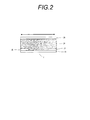
- the arrows in FIG. 2 indicate the direction of the temperature difference applied when the element is used.
- thermoelectric conversion material The thermoelectric conversion performance of the thermoelectric conversion material or the thermoelectric conversion element can be measured by a figure of merit ZT represented by the following formula (A).
- ZT figure of merit
- factors other than electrical conductivity greatly affect thermoelectric conversion performance, so it is actually unknown whether a material with high conductivity generally functions effectively as a thermoelectric conversion material. It is.
- the thermoelectric conversion material of the present invention can realize high conductivity without lowering the thermoelectromotive force, and has high thermoelectric conversion performance sufficient for use as a thermoelectric conversion material, as demonstrated in Examples described later.
- thermoelectric conversion material of the present invention contains carbon nanotubes and a polythiophene polymer composed of a repeating unit represented by the following general formula (1).
- a polythiophene polymer composed of a repeating unit represented by the following general formula (1).
- a carbon nanotube (hereinafter also referred to as CNT) includes a single-walled CNT in which a single carbon film (graphene sheet) is wound in a cylindrical shape, a double-walled CNT in which two graphene sheets are wound in a concentric shape, In addition, there are multi-layer CNTs in which a plurality of graphene sheets are concentrically wound.
- single-walled CNTs, double-walled CNTs, and multilayered CNTs may be used alone, or two or more kinds may be used in combination.
- Single-walled CNTs may be semiconducting or metallic, and both may be used in combination.
- the CNT may contain a metal or the like, or may contain a molecule such as fullerene.
- the thermoelectric conversion material of the present invention may contain nanocarbons such as carbon nanohorns, carbon nanocoils, and carbon nanobeads in addition to CNTs.
- CNT can be produced by an arc discharge method, a chemical vapor deposition method (hereinafter referred to as a CVD method), a laser ablation method, or the like.
- the CNT used in the present invention may be obtained by any method, but is preferably obtained by an arc discharge method and a CVD method.
- a CVD method chemical vapor deposition method
- fullerene, graphite, and amorphous carbon are produced as by-products at the same time, and catalyst metals such as nickel, iron, cobalt, and yttrium remain.
- purification is preferably performed.
- the method for purifying CNTs is not particularly limited, but acid treatment with nitric acid, sulfuric acid, etc., and ultrasonic treatment are effective for removing impurities.
- CNT can be used as it is.
- CNT since CNT is generally produced in a string shape, it may be cut into a desired length depending on the application.
- CNTs can be cut into short fibers by acid treatment with nitric acid, sulfuric acid or the like, ultrasonic treatment, freeze pulverization method or the like.
- not only cut CNTs but also CNTs produced in the form of short fibers in advance can be used in the same manner.
- Such short fibrous CNTs for example, form a catalytic metal such as iron or cobalt on a substrate, and thermally decompose the carbon compound at 700 to 900 ° C.
- the short fiber CNTs thus produced can be taken out by a method such as peeling off from the substrate.
- the short fibrous CNTs can be obtained by supporting a catalytic metal on a porous support such as porous silicon or an anodic oxide film of alumina and growing the CNTs on the surface by the CVD method. Even with a method of producing CNTs on a substrate by using CVD in an argon / hydrogen gas flow using molecules such as iron phthalocyanine containing a catalytic metal in the molecule, it is possible to produce oriented short fiber CNTs. Can do. Furthermore, short fiber CNTs oriented on the SiC single crystal surface can be obtained by an epitaxial growth method.
- the average length of the CNTs used in the present invention is not particularly limited, but from the viewpoints of manufacturability, film formability, conductivity, etc., the average length of the CNTs is preferably 0.01 ⁇ m or more and 1000 ⁇ m or less. More preferably, it is 1 ⁇ m or more and 100 ⁇ m or less.
- the diameter of the CNT used in the present invention is not particularly limited, but from the viewpoint of durability, transparency, film formability, conductivity, etc., the diameter of the CNT is preferably 0.4 nm or more and 100 nm or less, more preferably 50 nm. Hereinafter, it is more preferably 15 nm or less.
- the content of CNT in the thermoelectric conversion material is preferably 2 to 60% by mass, more preferably 5 to 40% by mass, and particularly preferably 8 to 30% by mass in the total solid content. .
- the polythiophene polymer used for the thermoelectric conversion material of the present invention has an alkyl-substituted thiophene structure represented by the following general formula (1) as a repeating unit. Since the polythiophene polymer has a molecular structure having a conjugated polymer main chain by forming a polymer main chain linked at positions 2 and 5 of the thiophene ring, it functions as a conductive polymer.
- R 1 and R 2 each independently represents an alkyl group having 1 to 20 carbon atoms.
- the alkyl group for R 1 and R 2 may be either a linear alkyl group or a branched alkyl group. Specifically, methyl, ethyl, propyl, butyl, pentyl, hexyl, heptyl, octyl, nonyl, decyl, undecyl, dodecyl, tridecyl, tetradecyl as linear alkyl groups Group, pentadecyl group, hexadecyl group, heptadecyl group, octadecyl group, nonadecyl group, eicosyl group, and branched alkyl groups such as isopropyl group, isobutyl group, isoamyl group, s-butyl group, t-butyl group, 2-methylbutyl group And 2-
- R 1 is preferably an alkyl group having 1 to 4 carbon atoms, more preferably a linear alkyl group having 1 to 3 carbon atoms, and particularly preferably a methyl group.
- R 2 is preferably an alkyl group having 4 to 12 carbon atoms, more preferably a branched alkyl group having 4 to 12 carbon atoms, such as 2-methylhexyl group, 2-ethylhexyl group, 2-methyl An octyl group and a 2-ethyloctyl group are more preferable, and a 2-ethylhexyl group is particularly preferable.
- alkyl groups in which R 1 and R 2 are different are preferable, and R 1 is a linear alkyl group and R 2 is more preferably a branched alkyl group.
- R 1 is an alkyl group having 1 to 4 carbon atoms and R 2 is an alkyl group having 4 to 12 carbon atoms, more preferably R 1 is 1 to 4 carbon atoms.
- a straight chain alkyl group of 3 and R 2 is a combination of branched alkyl groups having 4 to 12 carbon atoms, more preferably R 1 is a methyl group and R 2 is a 2-methylhexyl group, 2-ethylhexyl group, 2- It is a combination of a methyl octyl group or a 2-ethyloctyl group, and particularly preferably a combination of R 1 is a methyl group and R 2 is a 2-ethylhexyl group.
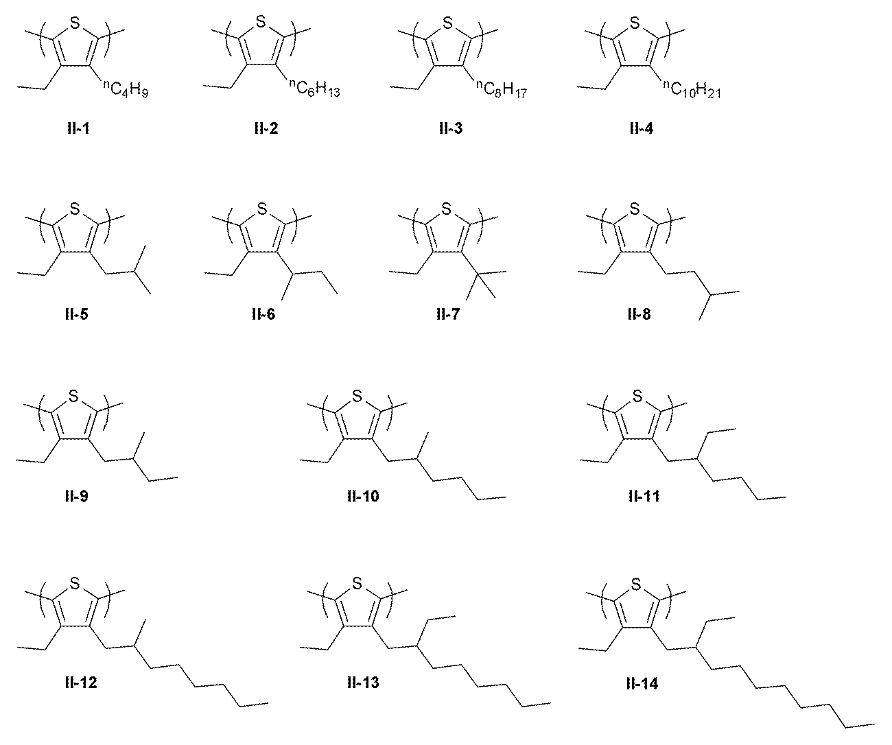
- polythiophene polymer represented by the general formula (1) Specific examples of the polythiophene polymer represented by the general formula (1) are shown below, but the present invention is not limited thereto.
- the polythiophene polymer used in the present invention has a disubstituted structure in which both the 3-position and 4-position of the thiophene ring as a repeating unit are substituted with an alkyl group. To do. Since the thiophene ring is active at the 2nd and 5th positions, the polymerization reaction proceeds selectively at the 2nd and 5th positions under normal conditions, and polythiophene-2,5-diyl is obtained.
- the resulting polythiophene main chain is greatly twisted due to steric repulsion between the thiophene rings.
- the twist of the polythiophene main chain having a thiophene ring having a disubstituted structure as a structural unit is compared with that of a polythiophene having a thiophene ring having a monosubstituted structure in which only one of the 3-position or 4-position of the thiophene ring is substituted as a structural unit. , Bigger.
- Examples of the method for measuring the degree of twist of the polythiophene main chain include a method for measuring the ionization potential of polythiophene.
- the ionization potential represents energy required for ionization of molecules, and corresponds to the energy level of the highest occupied orbit (HOMO).
- HOMO highest occupied orbit
- the ionization potential of a polyalkylthiophene having a mono-substituted structure is about 5.2 eV, and the degree of conjugation of the polythiophene main chain is smaller as the value positively larger than this value (the HOMO level is deeper). That is, it can be determined that the twisting degree of the polythiophene main chain is large.
- Examples of methods for measuring the ionization potential include electrochemical techniques such as photoelectron spectroscopy and cyclic voltammetry.
- thermoelectric conversion material of the present invention can achieve high conductivity by including a polymer composed of a repeating unit of a polythiophene structure having a 2-substituted structure together with CNT.
- the reason is considered to be that the use of polythiophene having a large twist of the polymer main chain causes highly efficient carrier movement as described below.
- Carriers (holes) generated by the conductive polymer polythiophene (carrier mobility ⁇ 0.1 cm 2 / (V ⁇ s)) are injected into the CNT, and the carrier has high carrier mobility (carrier mobility ⁇ 30000 cm 2 / (V ⁇ s)), which moves at a high speed in the CNT, high conductivity is exhibited.
- the hole injection property to the CNT is further increased, and as a result, the conductivity is estimated to be further improved.
- the number of repeating units represented by the general formula (1) is preferably about 4 to 2,000.
- the molecular weight is preferably 5,000 to 250,000, more preferably 10,000 to 200,000, and further preferably 15,000 to 170,000 in terms of weight average molecular weight.
- the weight average molecular weight can be measured by gel permeation chromatography (GPC).
- polythiophene polymer used in the present invention a commercially available product can be used, oxidation polymerization with iron chloride using 2,5-position unsubstituted thiophene as a raw material monomer, and 2,5-position Br group-substituted thiophene as a raw material monomer. It can also be synthesized by a method such as a polymerization method using a Ni (II) catalyst / Grignard reagent.
- the content of the polythiophene polymer in the thermoelectric conversion material is preferably 20 to 80% by mass, more preferably 30 to 75% by mass, and more preferably 35 to 70% by mass in the total solid content. Is particularly preferred.
- the thermoelectric conversion material of the present invention preferably contains a non-conjugated polymer in addition to the above-described CNT and polythiophene polymer.
- the non-conjugated polymer used for the thermoelectric conversion material is a polymer compound that does not exhibit conductivity due to the conjugated structure of the polymer main chain.
- the polymer main chain is composed of a ring, a group, or an atom selected from an aromatic ring (carbocyclic aromatic ring, heteroaromatic ring), an ethynylene bond, an ethenylene bond, and a hetero atom having a lone pair. It is a polymer other than the polymer.
- the type is not particularly limited as long as it is a non-conjugated polymer that satisfies such conditions, and a conventionally known non-conjugated polymer can be used.
- a polymer compound obtained by polymerizing a compound selected from the group consisting of vinyl compounds, (meth) acrylate compounds, carbonate compounds, ester compounds, amide compounds, imide compounds, fluorine compounds and siloxane compounds is used.
- vinyl compounds include styrene, vinyl pyrrolidone, vinyl carbazole, vinyl pyridine, vinyl naphthalene, vinyl phenol, vinyl acetate, styrene sulfonic acid, vinyl alcohol, vinyl triphenylamine and other vinyl arylamines, vinyl tributylamine.
- Vinyltrialkylamines such as, and the like.
- (meth) acrylate compounds include alkyl group-containing hydrophobic acrylates such as methyl acrylate, ethyl acrylate, propyl acrylate, and butyl acrylate, 2-hydroxyethyl acrylate, 1-hydroxyethyl acrylate, 2-hydroxypropyl acrylate, Acrylate monomers such as hydroxyl group-containing acrylates such as 3-hydroxypropyl acrylate, 1-hydroxypropyl acrylate, 4-hydroxybutyl acrylate, 3-hydroxybutyl acrylate, 2-hydroxybutyl acrylate, 1-hydroxybutyl acrylate, etc. And methacrylate monomers in which the acryloyl group is replaced with a methacryloyl group.
- polymers obtained by polymerizing a carbonate compound include general-purpose polycarbonate composed of bisphenol A and phosgene, Iupizeta (trade name, manufactured by Mitsubishi Gas Chemical Co., Ltd.), Panlite (trade name, manufactured by Teijin Chemicals Ltd.), and the like. It is done.
- ester compound include lactic acid.
- polymers obtained by polymerizing ester compounds include Byron (trade name, manufactured by Toyobo Co., Ltd.) and the like.
- polymers obtained by polymerizing amide compounds include PA-100 (trade name, manufactured by T & K TOKA Corporation).
- polymer obtained by polymerizing an imide compound examples include Solpy 6,6-PI (trade name, manufactured by Solpy Kogyo Co., Ltd.).
- fluorine compound examples include vinylidene fluoride and vinyl fluoride.
- siloxane compound examples include diphenylsiloxane and phenylmethylsiloxane.
- the non-conjugated polymer may be a homopolymer or a copolymer. In the present invention, it is more preferable to use a polymer compound obtained by polymerizing a vinyl compound as the non-conjugated polymer.
- the content of the non-conjugated polymer in the thermoelectric conversion material is preferably 10 to 1500 parts by weight, more preferably 30 to 1200 parts by weight, with respect to 100 parts by weight of the polythiophene polymer. It is particularly preferable that it is in parts by mass.
- the non-conjugated polymer is preferably hydrophobic and more preferably has no hydrophilic group such as sulfonic acid or hydroxyl group in the molecule. Further, a non-conjugated polymer having a solubility parameter (SP value) of 11 or less is preferable.
- SP value solubility parameter
- non-conjugated polymers having an SP value of 11 or less include polyvinyl compounds such as polystyrene, polyvinyl naphthalene, and polyvinyl acetate, poly (meth) acrylates such as polymethyl acrylate, ethyl acrylate, propyl acrylate, and butyl acrylate, polyester compounds, and polycarbonate.
- Polyvinylidene fluoride, and the like are preferable, and polystyrene, polyvinyl naphthalene, polymethyl acrylate, and polycarbonate are more preferable.
- thermoelectric conversion material of the present invention preferably contains a solvent in addition to the above-described CNT and polythiophene polymer.
- the thermoelectric conversion material of the present invention is more preferably a CNT dispersion in which a polythiophene component is dissolved in a solvent and CNTs are dispersed.
- the solvent should just be able to disperse
- organic solvents such as alcohol, chloroform, aprotic polar solvents such as DMF, NMP, DMSO, chlorobenzene, dichlorobenzene, benzene, toluene, xylene, mesitylene, tetralin, tetramethylbenzene, pyridine
- aromatic solvents such as cyclohexanone, ketone solvents such as acetone and methylethylkenton, ether solvents such as diethyl ether, THF, t-butyl methyl ether, dimethoxyethane and diglyme
- halogen solvents such as chloroform.
- aprotic polar solvents such as DMF and NMP
- aromatic solvents such as dichlorobenzene, xylene, tetralin, mesitylene and tetramethylbenzene
- ether solvents such as THF.
- the solvent is preferably degassed in advance.
- the dissolved oxygen concentration in the solvent is preferably 10 ppm or less.
- Examples of the degassing method include a method of irradiating ultrasonic waves under reduced pressure, a method of bubbling an inert gas such as argon, and the like.
- the solvent is preferably dehydrated in advance.
- the amount of water in the solvent is preferably 1000 ppm or less, and more preferably 100 ppm or less.
- a dehydration method a known method such as a method using molecular sieve or distillation can be used.
- the amount of the solvent in the thermoelectric conversion material is preferably 60 to 99.95% by mass and more preferably 70 to 99.9% by mass with respect to the total solid content of the thermoelectric conversion material and the total mass of the solvent.
- the content is preferably 80 to 99.8% by mass.
- thermoelectric conversion material of the present invention may contain other components in addition to the above components.
- a surfactant can be contained.
- lithium hydroxide, ammonium persulfate, an ultraviolet absorber, a polymerization inhibitor, a leveling additive, a matting agent and the like can be contained.
- inorganic fine particles, polymer fine particles, silane coupling agents, waxes and the like can be contained.
- a binder polymer or the like can be contained.
- a fluorine compound or the like can be contained.
- an antioxidant, a light stabilizer, a heat stabilizer, a plasticizer, and the like may be appropriately contained.
- the content of these components is preferably about 0.1 to 15% by mass with respect to the total mass of the thermoelectric conversion material.
- thermoelectric conversion material of the present invention can be prepared by mixing the above components.
- CNT and a polythiophene polymer are added to a solvent and mixed, and each component is dissolved or dispersed.
- the order of addition and mixing of each component is not particularly limited, but it is preferable to add a predetermined amount of polythiophene polymer in a solvent in advance and then add and disperse a predetermined amount of CNT.
- a dispersion method such as a mechanical homogenizer method, a jaw crusher method, an ultracentrifugation method, a cutting mill method, an automatic mortar method, a disk mill method, a ball mill method, or an ultrasonic dispersion method can be used. Further, if necessary, two or more of these methods may be used in combination.
- a preferred combination of dispersion methods is a mechanical homogenizer method and an ultrasonic dispersion method. There is no limitation on the order of the combination, and there are a method of dispersing sequentially by different dispersion methods or a method of dispersing simultaneously by different dispersion methods.
- the dispersion is first performed by a dispersion method having a weak dispersion energy and then dispersed by a dispersion method having a second highest dispersion energy.
- a dispersion method having a weak dispersion energy it becomes possible to disperse CNTs at a high concentration without defects.
- thermoelectric conversion material can be prepared in the air, it is preferably performed in an inert atmosphere.
- An inert atmosphere refers to a state where the oxygen concentration is lower than the atmospheric concentration.
- the atmosphere has an oxygen concentration of 10% or less.
- Examples of the method for making the inert atmosphere include a method of substituting the atmosphere with a gas such as nitrogen or argon, which is preferably used.
- the temperature during preparation is preferably in the range of 0 ° C to 50 ° C.
- CNTs contained in the obtained thermoelectric conversion material may contain defective CNTs. Such CNT defects are preferably reduced in order to reduce the conductivity of the thermoelectric conversion material.
- the amount of CNT defects in the thermoelectric conversion material can be estimated by the ratio G / D of the G-band and D-band of the Raman spectrum. It can be estimated that the higher the G / D ratio, the less the amount of defects, the CNT material.
- the G / D ratio of the thermoelectric conversion material is preferably 10 or more, and more preferably 30 or more.
- thermoelectric conversion element The thermoelectric conversion element of this invention should just be formed using the thermoelectric conversion material of this invention for a thermoelectric conversion layer.
- the thermoelectric conversion layer is not particularly limited as long as the thermoelectric conversion layer is obtained by molding the thermoelectric conversion material on a substrate, and the thermoelectric conversion material of the present invention has good CNT dispersibility. Therefore, the thermoelectric conversion layer can be formed by coating and forming a film on the substrate. Examples of the thermoelectric conversion material coating method include known coating methods such as spin coating, extrusion die coating, blade coating, bar coating, screen printing, stencil printing, roll coating, curtain coating, spray coating, dip coating, and ink jet printing. Can be used. After the coating process, if necessary, a heating process or a drying process may be provided to distill off the solvent and the like.
- thermoelectric conversion material ink jet printing method
- the ink jet printing method is a printing method in which ink is ejected from a nozzle and particulate ink is deposited on a substrate.
- a thermoelectric conversion layer can be formed by applying the thermoelectric conversion material of the present invention as an ink by an ink jet printing method.
- inkjet printing method There is no restriction
- the ink ejection method used in the ink jet apparatus There is no particular limitation on the ink ejection method used in the ink jet apparatus.
- an apparatus including an ink supply system and a temperature sensor is preferably used as the piezo-type ink jet apparatus.
- the ink supply system includes, for example, an original tank, supply piping, an ink supply tank immediately before the inkjet head, a filter, and a piezo-type inkjet head.
- Piezo-type ink jet heads can be driven so that ejection can be performed at 0.1 to 100 pl, preferably 0.5 to 20 pl.
- Droplets placed by ejection may be placed at intervals, or may be placed so that the droplets are coupled to each other, but from the viewpoint of making the thickness of the remaining film uniform and thin. It is preferable to be installed.
- the total amount of droplets varies depending on the pattern to be formed, and is adjusted so that the pattern and the remaining film have an appropriate thickness. Further, it is preferable to make the interval between the droplets non-uniform according to the density of the pattern.
- Specific examples of the ink jet apparatus having these functions include DMP-3000 and DMP-2831 manufactured by Fujifilm Dimatics.
- the ink jet apparatus can set the ink temperature at the time of ejection constant. From this viewpoint, it is preferable that the temperature of any part or all of the part from the ink supply tank to the ink jet head of the ink jet apparatus can be controlled.
- a temperature control method for example, it is preferable to provide a plurality of temperature sensors in each piping part and perform heating control according to the ink flow rate, the environmental temperature, and the like. The temperature sensor can be provided in the vicinity of the ink supply tank and the nozzle of the inkjet head.
- the viscosity of the thermoelectric conversion material is 0.5 mPa ⁇ s to 30 mPa ⁇ s at the temperature at the time of discharge in consideration of the discharge property from the ink jet nozzle. Is preferably 0.5 mPa ⁇ s to 20 mPa ⁇ s, more preferably 1 mPa ⁇ s to 15 mPa ⁇ s.
- the viscosity of the thermoelectric conversion material can be adjusted by appropriately increasing or decreasing the solid content or the solvent amount.
- the surface tension of the thermoelectric conversion material is preferably 20 mN / m to 40 mN / m, more preferably 23 mN / m to 35 mN / m.
- the surface tension of the thermoelectric conversion material can be adjusted by using a surfactant or the like.
- thermoelectric conversion layer In order to make the thermoelectric conversion layer have a desired thickness, it is also preferable to repeat inkjet printing of the thermoelectric conversion material. When performing repeatedly, it is preferable to provide a heating process and a drying process after performing inkjet printing to distill off the solvent and the like, and then perform inkjet printing.
- the substrate can be a substrate made of glass, transparent ceramics, metal, plastic film or the like.
- plastic film that can be used in the present invention include polyethylene terephthalate, polyethylene isophthalate, polyethylene naphthalate, polybutylene terephthalate, poly (1,4-cyclohexylenedimethylene terephthalate), polyethylene-2,6-phthalene dicarboxylate.
- Polycycloolefin films such as rate, polyester films such as polyester films of bisphenol A and iso and terephthalic acid, product names ZEONOR film (manufactured by Nippon Zeon), ARTON film (manufactured by JSR), Sumilite FS1700 (manufactured by Sumitomo Bakelite) , Product name Kapton (made by Toray DuPont), Apical (made by Kaneka), Ubilex (made by Ube Industries), Pomilan (made by Arakawa Chemical Co.), Polyester such as polycarbonate film such as Sose (manufactured by Teijin Chemicals), Elmec (manufactured by Kaneka), polyether ether ketone film such as product name Sumilite FS1100 (manufactured by Sumitomo Bakelite), polyphenyl such as product name Torelina (manufactured by Toray Industries, Inc.) Examples thereof include a sulfide film.
- polyethylene terephthalate polyethylene naphthalate
- various polyimides polycarbonate films, and the like are preferable from the viewpoints of availability, preferably heat resistance of 100 ° C. or higher, economy, and effects.
- a base material in which various electrode materials are provided on the pressure contact surface with the thermoelectric conversion layer.
- This electrode material includes transparent electrodes such as ITO and ZnO, metal electrodes such as silver, copper, gold, and aluminum, carbon materials such as CNT and graphene, organic materials such as PEDOT / PSS, and conductive fine particles such as silver and carbon.
- Dispersed conductive paste, conductive paste containing metal nanowires such as silver, copper, and aluminum can be used.
- thermoelectric conversion element of this invention should just have a thermoelectric conversion layer using the thermoelectric conversion material of this invention, and it does not specifically limit about the structure.
- it is an element provided with a base material (substrate) and a thermoelectric conversion layer provided on the base material, more preferably an element further having an electrode for electrically connecting them, more preferably
- the element includes a base material and a pair of electrodes on the base material, and a thermoelectric conversion layer is disposed between the pair of electrodes.
- Examples of the structure of the thermoelectric conversion element of the present invention include the structure of the element (1) shown in FIG. 1 and the element (2) shown in FIG. The element (1) shown in FIG.
- 1 includes a pair of electrodes including a first electrode (13) and a second electrode (15) on a first substrate (12), and the electrode of the present invention between the electrodes. It is an element provided with a thermoelectric conversion layer (14).
- the second electrode (15) is disposed on the surface of the second base material (16), and the first base material (12) and the second base material (16) are arranged on the outer sides of the metal facing each other. Plates (11 and 17) are arranged.
- a first electrode (23) and a second electrode (25) are disposed on a first base material (22), and a thermoelectric conversion layer (24) is disposed thereon. Is provided. 1 and 2, arrows indicate the direction of the temperature difference when the thermoelectric conversion element is used.
- thermoelectric conversion material of the present invention is provided in the form of a film (film) on a base material, and the base material functions as the first base material (12, 22).
- the above-mentioned various electrode materials are provided on the substrate surface (pressure contact surface with the thermoelectric conversion layer), and a thermoelectric conversion layer formed using the thermoelectric conversion material of the present invention is provided thereon. It is preferable.
- thermoelectric conversion layer one surface is covered with a base material.
- a base material (second base material (16, 26)) is preferably pressure-bonded from the viewpoint of protecting the film.
- the pressure bonding between the second base material and the thermoelectric conversion layer is preferably performed by heating to about 100 ° C. to 200 ° C. from the viewpoint of improving adhesion.
- the thickness of the thermoelectric conversion layer is preferably 0.1 ⁇ m to 1000 ⁇ m, more preferably 1 ⁇ m to 100 ⁇ m. By setting the film thickness within this range, it is easy to impart a temperature difference and increase in resistance within the film can be prevented.
- the thicknesses of the first and second base materials are preferably 30 to 3000 ⁇ m, more preferably 50 to 1000 ⁇ m, still more preferably 100 to 1000 ⁇ m, and particularly preferably 200 to 800 ⁇ m from the viewpoints of handleability and durability. It is. By setting the thickness of the base material within this range, the thermal conductivity does not decrease, and the film (thermoelectric conversion layer) is not easily damaged by an external impact.
- thermoelectric conversion layer in a thermoelectric conversion element, compared to a photoelectric conversion element such as an organic thin film solar cell element, the thermoelectric conversion layer may be applied and formed in one organic layer, and the element can be easily produced.
- thermoelectric conversion material of the present invention it is possible to increase the film thickness by about 100 to 1000 times compared with the element for organic thin film solar cells, and the chemical stability against oxygen and moisture in the air is improved To do.
- thermoelectric power generation article of the present invention uses the thermoelectric conversion element of the present invention as a power generation element. Specifically, it is preferable to use the thermoelectric conversion element of the present invention for applications such as generators such as hot spring thermal generators, solar thermal generators, waste heat generators, wristwatch power supplies, semiconductor drive power supplies, and small sensor power supplies.
- generators such as hot spring thermal generators, solar thermal generators, waste heat generators, wristwatch power supplies, semiconductor drive power supplies, and small sensor power supplies.
- polythiophenes 1 to 3 were commercially available from American DyeSource, and polythiophenes 11 to 13 were commercially available from Aldrich.
- the molecular weight of polythiophene was measured by GPC (gel permeation chromatography). O-Dichlorobenzene was added to each sample, dissolved at 145 ° C., and filtered through a 1.0 ⁇ m sintered filter to prepare a 0.15 wv% sample solution and used for the measurement. Measurements are as follows: apparatus: “Alliance GPC2000 (manufactured by Waters)”, column: TSKgel GMH6-HT ⁇ 2 + TSKgel GMH6-HTL ⁇ 2 (both 7.5 mm ID ⁇ 30 cm, manufactured by Tosoh Corporation), column temperature: 140 ° C. , Detector: differential refractometer, mobile phase: o-dichlorobenzene. The average molecular weight was determined. The molecular weight was constructed using standard polystyrene.
- the ionization potentials of the above polythiophenes 1 to 14 were measured by the following method.
- Preparation of polythiophene film To 10 mg of polythiophene, 1 mL of a THF-xylene (7: 3) solution was added and dissolved using an ultrasonic cleaner “US-2” (manufactured by Iuchi Seieido Co., Ltd., output 120 W, indirect irradiation).
- a glass substrate having a thickness of 1.1 mm and a size of 40 mm ⁇ 50 mm was ultrasonically cleaned in acetone and then UV-ozone treatment was performed for 10 minutes.
- a polythiophene film was prepared by spin-coating a polythiophene THF-xylene solution on this glass substrate (2000 rpm, 30 seconds) and then drying at room temperature.
- the ionization potential of the obtained polythiophene film was measured and evaluated by the following method. [Measurement of ionization potential]
- the ionization potential of polythiophene was measured by photoelectron spectroscopy in the atmosphere using a photoelectron spectrometer “AC-2” (manufactured by Riken Keiki Co., Ltd.).
- a positive ionization potential value indicates a state in which the conjugated system of the main chain of the polythiophene polymer is broken, and thus the twist of the polymer main chain is large.
- Example 1-1 10 mg of o-dichlorobenzene was added to 10 mg of ASP-100F (manufactured by Hanwha Nanotech, purity 95%) and 25 mg of polythiophene 1 as single-walled carbon nanotubes, and stirred for 20 minutes with a mechanical stirring device. Then, using an ultrasonic cleaner “US-2” (manufactured by Iuchi Seieido Co., Ltd., output 120 W, indirect irradiation), ultrasonic dispersion is performed at 30 ° C. for 40 minutes, so that the thermoelectric conversion material o-dichlorobenzene. A solution was made.
- thermoelectric conversion layer having a thickness of about 50 nm was formed by spin-coating the o-dichlorobenzene solution of the thermoelectric conversion material on the glass substrate (1500 rpm, 30 seconds) and drying at room temperature under vacuum conditions for 3 hours.
- the conductivity and CNT dispersibility of the obtained thermoelectric conversion layer were measured and evaluated by the following methods. The results are shown in Table 1.
- CNT dispersibility The CNT dispersibility was visually evaluated according to the following three-stage criteria. 1: Time required for CNT dispersion is shorter than 5 minutes 2: Time required for CNT dispersion is 5 minutes or more, shorter than 15 minutes 3: Time required for CNT dispersion is 15 minutes or more
- thermoelectric conversion layer was formed and evaluated in the same manner as in Example 1-1 except that the type of polythiophene was changed as shown in Table 1 in Example 1-1. The results are shown in Table 1.
- Example 1-8 Example 1-1 was the same as Example 1-1 except that 0.5 mg of ASP-100F (manufactured by Hanwha nanotech, purity 95%) and 34.5 mg of polythiophene 1 were used as single-walled carbon nanotubes. Then, a thermoelectric conversion layer was formed and evaluated.
- ASP-100F manufactured by Hanwha nanotech, purity 95%)
- polythiophene 1 34.5 mg
- thermoelectric conversion layer was formed and evaluated in the same manner as in Example 1-1 except that the type of polythiophene was changed as shown in Table 1 in Example 1-1. The results are shown in Table 1.
- Example 1-1 was the same as Example 1-1 except that 0.5 mg of ASP-100F (manufactured by Hanwha nanotech, purity 95%) and 34.5 mg of polythiophene 11 were used as the single-walled carbon nanotubes. Then, a thermoelectric conversion layer was formed and evaluated.
- Examples 1-1 to 1-8 using a polythiophene polymer in which both the 3-position and 4-position of the thiophene ring are substituted with an alkyl group and a thermoelectric conversion material containing CNT are as follows:
- the main chain of the polythiophene polymer has a large twist, high conductivity, good CNT dispersibility, and few CNT defects.
- Example 2-1 Nitoflon No. having a thickness of 300 ⁇ m.
- 901UL manufactured by Nitto Denko Corporation
- a mold was prepared on a glass substrate.
- An o-dichlorobenzene solution of a thermoelectric conversion material produced in the same manner as in Example 1-1 was poured into the mold, dried at room temperature, and then annealed on a hot plate at a temperature of 80 ° C. for 10 minutes.
- a thermoelectric conversion layer having a thickness of 2.0 ⁇ m was formed to produce a thermoelectric conversion element.
- the conductivity, thermoelectric properties, and film formability of the obtained thermoelectric conversion element were measured and evaluated by the following methods. The results are shown in Table 2.
- thermoelectric property measuring device MODEL RZ2001i manufactured by Ozawa Science Co., Ltd.
- V / K Seebeck coefficient
- S / cm conductivity
- Example 2-1 the o-dichlorobenzene solution of the thermoelectric conversion material produced in the same manner as in Examples 1-2 to 1-7 was used as the thermoelectric conversion material, in the same manner as in Example 2-1, Thermoelectric conversion elements were prepared and evaluated.
- Example 2-1 the o-dichlorobenzene solution of the thermoelectric conversion material produced in the same manner as in Comparative Examples 1-1 to 1-4 was used as the thermoelectric conversion material. Thermoelectric conversion elements were prepared and evaluated.
- Example 3-1 Preparation of carbon nanotube dispersion paste Polythiophene 2 (manufactured by American DyeSource) 720 mg, o-dichlorobenzene 40 ml, and ultrasonic cleaner “US-2” (manufactured by Inoue Seiei Co., Ltd., output 120 W, indirect irradiation) A polythiophene solution 3-1 was produced under the conditions of 10 minutes at 40 ° C. Next, 960 mg of ASP-100F (manufactured by Hanwha Nanotech, purity 95%) as a single-walled carbon nanotube was added to the solution 3-1, and an ultrasonic homogenizer VC-750 (manufactured by SONICS & MATERIALS.
- thermoelectric conversion layer 3-1 The carbon nanotube dispersion paste 3-1 prepared above was formed on a substrate to form a thermoelectric conversion layer. Specifically, an ultrasonic cleaning in isopropyl alcohol followed by UV-ozone treatment for 10 minutes on a glass substrate having a thickness of 1.1 mm has an opening 13 ⁇ 13 mm formed by laser processing and has a thickness of 2 mm. The metal mask was put on. Next, after injecting the carbon nanotube dispersion paste 3-1 prepared above into the opening, the metal mask is removed, and then the glass substrate is heated and dried on a hot plate at 80 ° C. to form the thermoelectric conversion layer 3-1. The film was formed, and its film formability, conductivity, and thermoelectric properties were evaluated.
- thermoelectric conversion element shown in FIG. 3 was produced using the carbon nanotube dispersion paste 3-1 prepared above. More specifically, after ultrasonic cleaning in isopropyl alcohol, a metal mask having an opening of 20 ⁇ 20 mm formed by etching on a glass substrate (32) having a size of 40 ⁇ 50 mm and a thickness of 1.1 m is used. Electrode 1 (33) was formed by depositing (30 and 31) a chromium film having a thickness of 100 nm and then a gold film having a thickness of 100 nm by plating.
- thermoelectric conversion layer 3-1 was formed on the electrode 1 by heating and drying on the plate.
- conductive paste Dotite D-550 manufactured by Fujikura Kasei, silver paste is applied by screen printing to form an electrode 2 (35) on the thermoelectric conversion layer 3-1, and the thermoelectric conversion element 3- 1 (3) was produced and its thermoelectromotive force was evaluated.
- Test method [CNT dispersibility] The carbon nanotube dispersion paste was dropped on a slide glass, placed on a cover glass, visually observed, and evaluated according to the following four criteria. 1: No black aggregate was observed. 2: Black aggregates having a size of less than 0.5 mm were observed. 3: Black aggregates having a size of 0.5 mm or more and less than 1 mm were observed. 4: The amount of aggregates exceeding the standard 3 was observed.
- thermoelectric conversion layer is 1.5 times or less compared to the opening of the metal mask.
- the size of the thermoelectric conversion layer is larger than 1.5 times compared to the opening of the metal mask.
- Less than 3 times The size of the thermoelectric conversion layer is 2.0 times larger than the opening of the metal mask
- thermoelectromotive force of the thermoelectric conversion element is the digital multimeter R6581 (manufactured by Advantest), which is a voltage difference generated between the electrode 1 and the electrode 2 when the glass substrate of the thermoelectric conversion element is heated with a hot plate having a surface temperature of 80 ° C. Measured with Based on the measured values, evaluation was made relative to the following Comparative Example 3-1.
- thermoelectric conversion layer and a thermoelectric conversion element were produced in the same manner as in Example 3-1, except that the polythiophene 2 was changed to the same amount of polythiophene 4 or 5 in Example 3-1, and its characteristics were evaluated. .
- Example 3-1 Comparative Example 3-1 In Example 3-1, except that polythiophene 2 was changed to the same amount of polythiophene 12, a comparative thermoelectric conversion layer and a thermoelectric conversion element were produced in the same manner as in Example 3-1, and the characteristics were evaluated. .
- Examples 3-1 to 3 having a polythiophene polymer in which both the 3-position and 4-position of the thiophene ring are substituted with an alkyl group, and CNT and a thermoelectric conversion layer containing a non-conjugated polymer 3-3 was excellent in CNT dispersibility and film formability, and was excellent in conductivity, thermoelectric properties (PF) and thermoelectromotive force.
- Examples 3-2 and 3-3 using polythiophene in which one of the substituents of the thiophene ring is a branched alkyl group the CNT dispersibility was further improved.
- Comparative Example 3-1 using polythiophene in which either the 3-position or the 4-position of the thiophene ring was a hydrogen atom had low conductivity.
- Example 4-1 To 360 mg of polythiophene 2, 30 ml of o-dichlorobenzene was added, and a polythiophene solution 4-1 was prepared using an ultrasonic cleaner “US-2” (manufactured by Inoue Seieido Co., Ltd., output 120 W, indirect irradiation). . Next, 480 mg of KH SWCNT HP (manufactured by KH Chemicals, purity 80%) is added as a single-walled carbon nanotube to the solution 4-1, and an ultrasonic homogenizer VC-750 (manufactured by SONICS & MATERIALS. Inc., tapered microchip (probe diameter 6.
- a carbon nanotube dispersion liquid 4-1 0.86 g of poly (2-vinylnaphthalene) (weight average molecular weight 175,000, manufactured by Aldrich) as a non-conjugated polymer is added to Dispersion 4-1, and dissolved in a hot bath at 50 ° C.
- the carbon nanotube dispersion paste precursor 4-1 was prepared by stirring with a self-revolving stirrer ARE-250 (manufactured by Sinky) at a rotation speed of 2200 rpm and a stirring time of 15 minutes.
- the precursor 4-1 was turned back 15 times using a three-roll mill disperser BR-100V (manufactured by Imex) under the condition of a rotation ratio of 1: 1.7: 2.9, and the carbon nanotube dispersion paste 4- 1 was prepared.
- the CNT content in the solid content of this paste was 28.2% by mass, and the content of polythiophene was 21.1% by mass.
- the CNT dispersibility of the dispersion paste 4-1 was evaluated in the same manner as in Example 3-1.
- Example 4-2 A carbon nanotube dispersion paste 4-2 was prepared in the same manner as in Example 4-1, except that the same amount of polythiophene 4 was used instead of polythiophene 2 in Example 4-1.
- Example 4-3 In Example 4-2, the same amount of PC-Z type polycarbonate (manufactured by Teijin Chemicals Ltd., product name “Panlite TS-2020”) was used instead of poly (2-vinylnaphthalene). In the same manner as in 4-2, a carbon nanotube dispersion paste 4-3 was produced.
- PC-Z type polycarbonate manufactured by Teijin Chemicals Ltd., product name “Panlite TS-2020”
- thermoelectric conversion layer was obtained in the same manner as in Example 3-1, except that the carbon nanotube dispersion paste 3-1 in Example 3-1 was changed to each of the pastes 4-1 to 4-3 produced above.
- thermoelectric conversion element was prepared and its characteristics were evaluated in the same manner as in Example 3-1. The results are shown in Table 4.
- Examples 4-2 and 4-3 using polythiophene in which one of the substituents of the thiophene ring is a branched alkyl group further improved the CNT dispersibility or film formability.
- thermoelectric conversion element was produced using a polyethylene terephthalate (hereinafter referred to as PET) film produced below as a substrate.
- PET polyethylene terephthalate
- Adhesive Layer After both surfaces of the obtained support were subjected to corona discharge treatment under the condition of 730 J / m 2 , an adhesive layer coating liquid A having the following composition was applied to both surfaces at a coating amount of 4.4 cm 3 / m. 2 was applied by the bar coating method. And this was dried at 160 degreeC for 1 minute, and the laminated sheet (electric conductor) in which the contact bonding layer was formed on both surfaces of the support body was obtained by forming an contact bonding layer.
- Example 4-1 was the same as Example 4-1, except that polystyrene having the same polymerization degree of 2,000 (manufactured by Wako Pure Chemical Industries) was used instead of poly (2-vinylnaphthalene). Similarly, a carbon nanotube dispersion paste 5-1 was produced.
- thermoelectric conversion layer 5-1 was formed on the electrode 1 by heating and drying above.
- thermoelectric conversion element 5-1 thermoelectric conversion element 5-1.
- conductive paste dotite D-550 manufactured by Fujikura Kasei Co., Ltd., silver paste
- electrode 2 is formed on thermoelectric conversion layer 5-1, thereby producing thermoelectric conversion element 5-1.
- a voltage difference generated between the electrode 1 and the electrode 2 when the film substrate of the thermoelectric conversion element is heated with a hot plate having a surface temperature of 80 ° C. is measured with a digital multimeter R6581 (manufactured by Advantest), a voltage difference is generated. Confirmed.
- Example 5-2 A carbon nanotube dispersion paste 5-2 was produced in the same manner as in Example 5-1, except that the same amount of polythiophene 4 was used instead of polythiophene 2 in Example 5-1. Subsequently, a thermoelectric conversion layer and a thermoelectric conversion element 5-2 were produced in the same manner as in Example 5-1, except that the carbon nanotube dispersion paste 5-2 was used instead of the carbon nanotube dispersion paste 5-1.
- a voltage difference generated between the electrode 1 and the electrode 2 when the film substrate of the thermoelectric conversion element is heated with a hot plate having a surface temperature of 80 ° C. is measured with a digital multimeter R6581 (manufactured by Advantest), a voltage difference is generated. Confirmed.
- Example 6-1 A thermoelectric conversion material o-dichlorobenzene solution was prepared in the same manner as in Example 1-1. This solution was printed on a glass substrate in a pattern of 8 mm ⁇ 8 mm using an inkjet printing apparatus.
- the inkjet printing apparatus used was an inkjet printer: DMP-2831, manufactured by Fujifilm Dimatics, and the pattern was formed on the glass substrate by ejecting the solution with a droplet amount of 10 pl per nozzle. At this time, the solution to be discharged was heated in the apparatus so as to be 40 ° C. After pattern formation, heating was performed at 120 ° C.
- thermoelectric conversion layer having a thickness of 2.0 ⁇ m to produce a thermoelectric conversion element.
- the thermoelectric characteristics of the obtained thermoelectric conversion element were evaluated in the same manner as in Example 2-1.
- Example 6-1 the o-dichlorobenzene solution of the thermoelectric conversion material was changed to the o-dichlorobenzene solution of the thermoelectric conversion material prepared in Examples 1-2 to 1-7. Similarly, a thermoelectric conversion element was produced and evaluated in the same manner as in Example 6-1.
- Table 5 shows the thermoelectric characteristic values of Examples 6-1 to 6-7 and the thermoelectric characteristic values of Examples 2-1 to 2-7 side by side.
- thermoelectric conversion element in which the thermoelectric conversion layer is formed by the ink jet printing method is poured into the mold and thermoelectric conversion is performed. Compared with the thermoelectric conversion element in which the layer was formed, high thermoelectric characteristics were exhibited.
- Electrode 1 (conductive paste)
Landscapes
- Chemical & Material Sciences (AREA)
- Health & Medical Sciences (AREA)
- Chemical Kinetics & Catalysis (AREA)
- Medicinal Chemistry (AREA)
- Polymers & Plastics (AREA)
- Organic Chemistry (AREA)
- Engineering & Computer Science (AREA)
- Manufacturing & Machinery (AREA)
- Materials Engineering (AREA)
- Nanotechnology (AREA)
- Compositions Of Macromolecular Compounds (AREA)
- Carbon And Carbon Compounds (AREA)
Description
本発明は、カーボンナノチューブを含有する熱電変換材料、これを用いた熱電変換素子及び熱電発電用物品に関する。また、本発明は、熱電変換素子の製造方法に関する。
近年、地球環境に配慮して、従来の化石エネルギーから再生可能エネルギーへの移行が求められてきている。再生可能エネルギーとしては、太陽光発電、風力発電、波力発電、振動発電、熱電発電等があるが、なかでも熱電発電は、熱エネルギーを直接電力に変換することができ、太陽熱発電、地熱発電、温水熱発電、工業炉や自動車からの排熱等、未利用の膨大な熱エネルギーを有効活用できる点で注目されている。また、熱電発電は、熱エネルギーを直接電力に変換することができ、可動部を必要としないため、体温で作動する腕時計や僻地用電源、宇宙用電源等に実用化されている。
熱電発電には、熱エネルギーと電気エネルギーを相互に変換することができる熱電変換材料、これを成形・加工してなる熱電変換素子(熱電発電素子)が用いられる。熱電変換効率の観点から、熱電変換材料として実用化段階にあるのは現在のところ無機材料である。しかし、これらの無機材料は材料自体が高価であったり、有害物質を含んでいたり、または、熱電変換素子への加工工程が複雑である等の問題を有している。そのため、比較的廉価に製造でき、成膜等の加工も容易な有機熱電変換材料の研究が進められている。例えば、特許文献1,2には、カーボンナノチューブを用いた熱電変換材料が報告されている。
本発明は、熱電変換性能に優れた熱電変換材料、これを用いた熱電変換素子及び熱電発電用物品、並びに熱電変換素子の製造方法を提供することを課題とする。
本発明者らはさらに、有機熱電変換材料について鋭意検討を行った。その結果、カーボンナノチューブと、チオフェン環の3位と4位がともにアルキル基で置換されたポリチオフェン重合体とを含有する組成物が、優れた熱電変換性能を示し、熱電変換材料として有用であることを見出した。当該材料は、高い導電性とともに、熱電変換に要求される熱起電力を備え、優れた熱電変換性能を示すものであった。本発明は、これらの知見に基づき成されたものである。
すなわち、上記の課題は、以下の熱電変換材料、熱電変換素子、熱電発電用物品、及び熱電変換素子の製造方法により達成された。
<1> カーボンナノチューブと、下記一般式(1)で表される繰り返し単位からなるポリチオフェン重合体とを含有する熱電変換材料。
<1> カーボンナノチューブと、下記一般式(1)で表される繰り返し単位からなるポリチオフェン重合体とを含有する熱電変換材料。

一般式(1)中、R1及びR2はそれぞれ独立に炭素原子数1~20のアルキル基を表す。
<2> 一般式(1)において、R2が炭素原子数4~12のアルキル基である<1>に記載の熱電変換材料。
<3> 一般式(1)において、R1が炭素原子数1~4のアルキル基である<1>又は<2>に記載の熱電変換材料。
<4> 一般式(1)において、R2が炭素原子数4~12の分岐アルキル基である<1>~<3>のいずれか1つに記載の熱電変換材料。
<5> 一般式(1)において、R1が炭素原子数1~3の直鎖アルキル基である<1>~<4>のいずれか1つに記載の熱電変換材料。
<6> 一般式(1)において、R2が2-メチルヘキシル基、2-エチルヘキシル基、2-メチルオクチル基、又は2-エチルオクチル基である<1>~<5>のいずれか1つに記載の熱電変換材料。
<7> 一般式(1)において、R2が2-エチルヘキシル基である<1>~<6>のいずれか1つに記載の熱電変換材料。
<8> 一般式(1)において、R1がメチル基である<1>~<7>のいずれか1つに記載の熱電変換材料。
<9> 熱電変換材料の全固形分中に、カーボンナノチューブを2~60質量%、ポリチオフェン重合体を20~80質量%含有する<1>~<8>のいずれか1つに記載の熱電変換材料。
<10> さらに非共役系高分子を含む、<1>~<9>のいずれか1つに記載の熱電変換材料。
<11> さらに溶媒を含む、<1>~<10>のいずれか1つに記載の熱電変換材料。
<12> <1>~<11>のいずれか1つに記載の熱電変換材料を熱電変換層に用いた熱電変換素子。
<13> 熱電変換層がインクジェット印刷法を用いて形成された、<12>に記載の熱電変換素子。
<14> 基材と、該基材上に設けられた熱電変換層とを備えた<12>又は<13>に記載の熱電変換素子。
<15> さらに電極を有する<12>~<14>のいずれか1つに記載の熱電変換素子。
<16> <12>~<15>のいずれか1つに記載の熱電変換素子を用いた熱電発電用物品。
<17> <1>~<11>のいずれか1つに記載の熱電変換材料を基材上にインクジェット印刷法で印刷して熱電変換層を設ける工程を含む、熱電変換素子の製造方法。
<2> 一般式(1)において、R2が炭素原子数4~12のアルキル基である<1>に記載の熱電変換材料。
<3> 一般式(1)において、R1が炭素原子数1~4のアルキル基である<1>又は<2>に記載の熱電変換材料。
<4> 一般式(1)において、R2が炭素原子数4~12の分岐アルキル基である<1>~<3>のいずれか1つに記載の熱電変換材料。
<5> 一般式(1)において、R1が炭素原子数1~3の直鎖アルキル基である<1>~<4>のいずれか1つに記載の熱電変換材料。
<6> 一般式(1)において、R2が2-メチルヘキシル基、2-エチルヘキシル基、2-メチルオクチル基、又は2-エチルオクチル基である<1>~<5>のいずれか1つに記載の熱電変換材料。
<7> 一般式(1)において、R2が2-エチルヘキシル基である<1>~<6>のいずれか1つに記載の熱電変換材料。
<8> 一般式(1)において、R1がメチル基である<1>~<7>のいずれか1つに記載の熱電変換材料。
<9> 熱電変換材料の全固形分中に、カーボンナノチューブを2~60質量%、ポリチオフェン重合体を20~80質量%含有する<1>~<8>のいずれか1つに記載の熱電変換材料。
<10> さらに非共役系高分子を含む、<1>~<9>のいずれか1つに記載の熱電変換材料。
<11> さらに溶媒を含む、<1>~<10>のいずれか1つに記載の熱電変換材料。
<12> <1>~<11>のいずれか1つに記載の熱電変換材料を熱電変換層に用いた熱電変換素子。
<13> 熱電変換層がインクジェット印刷法を用いて形成された、<12>に記載の熱電変換素子。
<14> 基材と、該基材上に設けられた熱電変換層とを備えた<12>又は<13>に記載の熱電変換素子。
<15> さらに電極を有する<12>~<14>のいずれか1つに記載の熱電変換素子。
<16> <12>~<15>のいずれか1つに記載の熱電変換素子を用いた熱電発電用物品。
<17> <1>~<11>のいずれか1つに記載の熱電変換材料を基材上にインクジェット印刷法で印刷して熱電変換層を設ける工程を含む、熱電変換素子の製造方法。
本発明において「~」を用いて表される数値範囲は、「~」の前後に記載される数値を下限値及び上限値として含む範囲を意味する。
また、本発明において置換基に関してxxx基というときには、そのxxx基に任意の置換基を有していてもよい。また、同一の符号で示された基が複数ある場合は、互いに同じであっても異なっていてもよい。
また、本発明において置換基に関してxxx基というときには、そのxxx基に任意の置換基を有していてもよい。また、同一の符号で示された基が複数ある場合は、互いに同じであっても異なっていてもよい。
本発明の熱電変換材料は、高い導電性とともに、熱電変換に要求される熱起電力を備え、優れた熱電変換性能を有する。当該熱電変換材料は、熱電変換素子や熱電発電用物品等の熱電変換用途に好適に用いることができる。
また、本発明の製造方法によれば、高い熱電特性を備えた熱電変換素子を製造することができる。
また、本発明の製造方法によれば、高い熱電特性を備えた熱電変換素子を製造することができる。
[熱電変換材料]
熱電変換材料や熱電変換素子の熱電変換性能は、下記式(A)で示される性能指数ZTによりはかることができる。下記式(A)から明らかなように、熱電変換性能向上には、熱起電力及び導電率を高めるとともに、熱伝導率を下げることが必要となる。このように熱電変換性能には、導電率以外のファクターが大きく影響するため、一般的に導電率が高いとされる材料であっても、熱電変換材料として有効に機能するかは実際のところ未知数である。本発明の熱電変換材料は、後述の実施例で実証されているように、熱起電力を低下させることなく高い導電性を実現でき、熱電変換材料として用いるに足る高い熱電変換性能を備える。
性能指数ZT=S2・σ・T/κ (A)
S(V/K):熱起電力(ゼーベック係数)
σ(S/m):導電率
κ(W/mK):熱伝導率
T(K):絶対温度
熱電変換材料や熱電変換素子の熱電変換性能は、下記式(A)で示される性能指数ZTによりはかることができる。下記式(A)から明らかなように、熱電変換性能向上には、熱起電力及び導電率を高めるとともに、熱伝導率を下げることが必要となる。このように熱電変換性能には、導電率以外のファクターが大きく影響するため、一般的に導電率が高いとされる材料であっても、熱電変換材料として有効に機能するかは実際のところ未知数である。本発明の熱電変換材料は、後述の実施例で実証されているように、熱起電力を低下させることなく高い導電性を実現でき、熱電変換材料として用いるに足る高い熱電変換性能を備える。
性能指数ZT=S2・σ・T/κ (A)
S(V/K):熱起電力(ゼーベック係数)
σ(S/m):導電率
κ(W/mK):熱伝導率
T(K):絶対温度
本発明の熱電変換材料は、カーボンナノチューブと、後述の一般式(1)で表される繰り返し単位からなるポリチオフェン重合体とを含有する。以下、本発明の熱電変換材料の各成分について説明する。
[カーボンナノチューブ]
カーボンナノチューブ(以下、CNTとも言う)には、1枚の炭素膜(グラフェン・シート)が円筒状に巻かれた単層CNT、2枚のグラフェン・シートが同心円状に巻かれた2層CNT、及び複数のグラフェン・シートが同心円状に巻かれた多層CNTがある。本発明においては、単層CNT、2層CNT、多層CNTを各々単独で用いてもよく、2種以上を併せて用いてもよい。特に、導電性及び半導体特性において優れた性質を持つ単層CNT及び2層CNTを用いることが好ましく、単層CNTを用いることがより好ましい。
単層CNTは、半導体性のものであっても、金属性のものであってもよく、両者を併せて用いてもよい。また、CNTには金属などが内包されていてもよく、フラーレン等の分子が内包されたものを用いてもよい。なお、本発明の熱電変換材料には、CNTの他に、カーボンナノホーン、カーボンナノコイル、カーボンナノビーズなどのナノカーボンが含まれてもよい。
カーボンナノチューブ(以下、CNTとも言う)には、1枚の炭素膜(グラフェン・シート)が円筒状に巻かれた単層CNT、2枚のグラフェン・シートが同心円状に巻かれた2層CNT、及び複数のグラフェン・シートが同心円状に巻かれた多層CNTがある。本発明においては、単層CNT、2層CNT、多層CNTを各々単独で用いてもよく、2種以上を併せて用いてもよい。特に、導電性及び半導体特性において優れた性質を持つ単層CNT及び2層CNTを用いることが好ましく、単層CNTを用いることがより好ましい。
単層CNTは、半導体性のものであっても、金属性のものであってもよく、両者を併せて用いてもよい。また、CNTには金属などが内包されていてもよく、フラーレン等の分子が内包されたものを用いてもよい。なお、本発明の熱電変換材料には、CNTの他に、カーボンナノホーン、カーボンナノコイル、カーボンナノビーズなどのナノカーボンが含まれてもよい。
CNTはアーク放電法、化学気相成長法(以下、CVD法という)、レーザー・アブレーション法等によって製造することができる。本発明に用いられるCNTは、いずれの方法によって得られたものであってもよいが、好ましくはアーク放電法及びCVD法により得られたものである。
CNTを製造する際には、同時にフラーレンや、グラファイトや、非晶性炭素が副生成物として生じ、また、ニッケル、鉄、コバルト、イットリウムなどの触媒金属も残存する。これらの不純物を除去するために、精製を行うことが好ましい。CNTの精製方法は特に限定されないが、硝酸、硫酸等による酸処理、超音波処理が不純物の除去には有効である。併せて、フィルターによる分離除去を行うことも、純度を向上させる観点からより好ましい。
CNTを製造する際には、同時にフラーレンや、グラファイトや、非晶性炭素が副生成物として生じ、また、ニッケル、鉄、コバルト、イットリウムなどの触媒金属も残存する。これらの不純物を除去するために、精製を行うことが好ましい。CNTの精製方法は特に限定されないが、硝酸、硫酸等による酸処理、超音波処理が不純物の除去には有効である。併せて、フィルターによる分離除去を行うことも、純度を向上させる観点からより好ましい。
精製の後、得られたCNTをそのまま用いることもできる。また、CNTは一般に紐状で生成されるため、用途に応じて所望の長さにカットして用いてもよい。CNTは、硝酸、硫酸等による酸処理、超音波処理、凍結粉砕法などにより短繊維状にカットすることができる。また、併せてフィルターによる分離を行うことも、純度を向上させる観点から好ましい。
本発明においては、カットしたCNTだけではなく、あらかじめ短繊維状に作製したCNTも同様に使用できる。このような短繊維状CNTは、例えば、基板上に鉄、コバルトなどの触媒金属を形成し、その表面にCVD法を用いて700~900℃で炭素化合物を熱分解してCNTを気相成長させることによって、基板表面に垂直方向に配向した形状で得られる。このようにして作製された短繊維状CNTは基板から剥ぎ取るなどの方法で取り出すことができる。また、短繊維状CNTは、ポーラスシリコンのようなポーラスな支持体や、アルミナの陽極酸化膜上に触媒金属を担持させ、その表面にCNTをCVD法にて成長させることもできる。触媒金属を分子内に含む鉄フタロシアニンのような分子を原料とし、アルゴン/水素のガス流中でCVDを行うことによって基板上にCNTを作製する方法でも、配向した短繊維状CNTを作製することができる。さらには、エピタキシャル成長法によってSiC単結晶表面に配向した短繊維状CNTを得ることもできる。
本発明においては、カットしたCNTだけではなく、あらかじめ短繊維状に作製したCNTも同様に使用できる。このような短繊維状CNTは、例えば、基板上に鉄、コバルトなどの触媒金属を形成し、その表面にCVD法を用いて700~900℃で炭素化合物を熱分解してCNTを気相成長させることによって、基板表面に垂直方向に配向した形状で得られる。このようにして作製された短繊維状CNTは基板から剥ぎ取るなどの方法で取り出すことができる。また、短繊維状CNTは、ポーラスシリコンのようなポーラスな支持体や、アルミナの陽極酸化膜上に触媒金属を担持させ、その表面にCNTをCVD法にて成長させることもできる。触媒金属を分子内に含む鉄フタロシアニンのような分子を原料とし、アルゴン/水素のガス流中でCVDを行うことによって基板上にCNTを作製する方法でも、配向した短繊維状CNTを作製することができる。さらには、エピタキシャル成長法によってSiC単結晶表面に配向した短繊維状CNTを得ることもできる。
本発明で用いるCNTの平均長さは特に限定されないが、製造容易性、成膜性、導電性等の観点から、CNTの平均長さが0.01μm以上1000μm以下であることが好ましく、0.1μm以上100μm以下であることがより好ましい。
本発明で用いるCNTの直径は特に限定されないが、耐久性、透明性、成膜性、導電性等の観点から、CNTの直径が0.4nm以上100nm以下であることが好ましく、より好ましくは50nm以下、さらに好ましくは15nm以下である。
本発明で用いるCNTの直径は特に限定されないが、耐久性、透明性、成膜性、導電性等の観点から、CNTの直径が0.4nm以上100nm以下であることが好ましく、より好ましくは50nm以下、さらに好ましくは15nm以下である。
熱電変換材料中のCNTの含有量は、全固形分中、2~60質量%であることが好ましく、5~40質量%であることがより好ましく、8~30質量%であることが特に好ましい。
[ポリチオフェン重合体]
本発明の熱電変換材料に用いるポリチオフェン重合体は、繰り返し単位として下記一般式(1)で表されるアルキル置換チオフェン構造を有する。当該ポリチオフェン重合体は、チオフェン環の2,5位で連結したポリマー主鎖を形成することで、共役系のポリマー主鎖を有する分子構造であるため、導電性高分子として機能する。
本発明の熱電変換材料に用いるポリチオフェン重合体は、繰り返し単位として下記一般式(1)で表されるアルキル置換チオフェン構造を有する。当該ポリチオフェン重合体は、チオフェン環の2,5位で連結したポリマー主鎖を形成することで、共役系のポリマー主鎖を有する分子構造であるため、導電性高分子として機能する。

一般式(1)において、R1及びR2はそれぞれ独立に炭素原子数1~20のアルキル基を表す。
R1及びR2のアルキル基は、直鎖アルキル基又は分岐アルキル基のいずれであってもよい。具体的には、直鎖アルキル基としてメチル基、エチル基、プロピル基、ブチル基、ペンチル基、ヘキシル基、ヘプチル基、オクチル基、ノニル基、デシル基、ウンデシル基、ドデシル基、トリデシル基、テトラデシル基、ペンタデシル基、ヘキサデシル基、ヘプタデシル基、オクタデシル基、ノナデシル基、エイコシル基が挙げられ、分岐アルキル基としてイソプロピル基、イソブチル基、イソアミル基、s-ブチル基、t-ブチル基、2-メチルブチル基、2-メチルヘキシル基、2-エチルヘキシル基、2-メチルオクチル基、2-エチルオクチル基等が例示できる。当該アルキル基は、さらに置換基を有していてもよいが、好ましくは無置換のアルキル基である。
R1及びR2のアルキル基は、直鎖アルキル基又は分岐アルキル基のいずれであってもよい。具体的には、直鎖アルキル基としてメチル基、エチル基、プロピル基、ブチル基、ペンチル基、ヘキシル基、ヘプチル基、オクチル基、ノニル基、デシル基、ウンデシル基、ドデシル基、トリデシル基、テトラデシル基、ペンタデシル基、ヘキサデシル基、ヘプタデシル基、オクタデシル基、ノナデシル基、エイコシル基が挙げられ、分岐アルキル基としてイソプロピル基、イソブチル基、イソアミル基、s-ブチル基、t-ブチル基、2-メチルブチル基、2-メチルヘキシル基、2-エチルヘキシル基、2-メチルオクチル基、2-エチルオクチル基等が例示できる。当該アルキル基は、さらに置換基を有していてもよいが、好ましくは無置換のアルキル基である。
R1は、炭素原子数1~4のアルキル基であることが好ましく、炭素原子数1~3の直鎖アルキル基であることがより好ましく、メチル基であることが特に好ましい。
R2は、炭素原子数4~12のアルキル基であることが好ましく、炭素原子数4~12の分岐アルキル基であることがより好ましく、2-メチルヘキシル基、2-エチルヘキシル基、2-メチルオクチル基、2-エチルオクチル基であることがさらに好ましく、2-エチルヘキシル基であることが特に好ましい。後述の実施例で示すように、R2に分岐アルキル基を導入すると、熱電変換材料中でのCNT分散性が向上し、良好な成膜性が得られる。
本発明においては、上記で示したように、R1とR2とが異なったアルキル基が好ましく、R1が直鎖のアルキル基でR2が分岐のアルキル基がより好ましい。
R1及びR2の好ましい組合せとしては、R1が炭素原子数1~4のアルキル基でR2が炭素原子数4~12のアルキル基であり、より好ましくはR1が炭素原子数1~3の直鎖アルキル基でR2が炭素原子数4~12の分岐アルキル基の組み合わせであり、さらに好ましくはR1がメチル基でR2が2-メチルヘキシル基、2-エチルヘキシル基、2-メチルオクチル基、又は2-エチルオクチル基の組み合わせであり、特に好ましくはR1がメチル基でR2が2-エチルヘキシル基の組み合わせである。
R2は、炭素原子数4~12のアルキル基であることが好ましく、炭素原子数4~12の分岐アルキル基であることがより好ましく、2-メチルヘキシル基、2-エチルヘキシル基、2-メチルオクチル基、2-エチルオクチル基であることがさらに好ましく、2-エチルヘキシル基であることが特に好ましい。後述の実施例で示すように、R2に分岐アルキル基を導入すると、熱電変換材料中でのCNT分散性が向上し、良好な成膜性が得られる。
本発明においては、上記で示したように、R1とR2とが異なったアルキル基が好ましく、R1が直鎖のアルキル基でR2が分岐のアルキル基がより好ましい。
R1及びR2の好ましい組合せとしては、R1が炭素原子数1~4のアルキル基でR2が炭素原子数4~12のアルキル基であり、より好ましくはR1が炭素原子数1~3の直鎖アルキル基でR2が炭素原子数4~12の分岐アルキル基の組み合わせであり、さらに好ましくはR1がメチル基でR2が2-メチルヘキシル基、2-エチルヘキシル基、2-メチルオクチル基、又は2-エチルオクチル基の組み合わせであり、特に好ましくはR1がメチル基でR2が2-エチルヘキシル基の組み合わせである。
一般式(1)で表されるポリチオフェン重合体の具体例を以下に示すが、本発明はこれらに限定されるものではない。



一般式(1)で表されるとおり、本発明で用いるポリチオフェン重合体は、繰り返し単位であるチオフェン環の3位及び4位がともにアルキル基で置換された、2置換構造をとることを特徴とする。
チオフェン環は2,5位が活性位のため、通常の条件では2,5位で選択的に重合反応が進行し、ポリチオフェン-2,5-ジイルが得られる。本発明で用いるような、2置換構造のチオフェン環を構造単位とするポリチオフェン-2,5-ジイルの場合、チオフェン環同士の立体反発によって、生じたポリチオフェン主鎖に大きなねじれが発生する。この2置換構造のチオフェン環を構造単位とするポリチオフェン主鎖のねじれは、チオフェン環の3位又は4位の一方のみが置換された1置換構造のチオフェン環を構造単位とするポリチオフェンの場合と比べ、より大きい。
チオフェン環は2,5位が活性位のため、通常の条件では2,5位で選択的に重合反応が進行し、ポリチオフェン-2,5-ジイルが得られる。本発明で用いるような、2置換構造のチオフェン環を構造単位とするポリチオフェン-2,5-ジイルの場合、チオフェン環同士の立体反発によって、生じたポリチオフェン主鎖に大きなねじれが発生する。この2置換構造のチオフェン環を構造単位とするポリチオフェン主鎖のねじれは、チオフェン環の3位又は4位の一方のみが置換された1置換構造のチオフェン環を構造単位とするポリチオフェンの場合と比べ、より大きい。
ポリチオフェン主鎖のねじれ度合いを測定する方法としては、ポリチオフェンのイオン化ポテンシャルを測定する方法が挙げられる。イオン化ポテンシャルとは、分子がイオン化されるのに必要なエネルギーを表し、最高占有軌道(HOMO)のエネルギー準位に相当する。一般に、有機分子の共役系が拡張して分子内の軌道間相互作用が増大するとHOMOのエネルギー準位は正に小さくなる。1置換構造のポリアルキルチオフェンのイオン化ポテンシャルは5.2eV程度であることが知られており、この値よりも正に大きい値(HOMO準位が深い)ほどポリチオフェン主鎖の共役の度合いが小さい、すなわちポリチオフェン主鎖のねじれ度合いが大きいと判断することができる。イオン化ポテンシャルの測定法としては、光電子分光法やサイクリックボルタンメトリーなどの電気化学的手法が挙げられる。
本発明の熱電変換材料は、CNTとともに、2置換構造のポリチオフェン構造の繰り返し単位からなる重合体を含むことで高い導電性を実現できると考えられる。その理由としては、ポリマー主鎖のねじれが大きなポリチオフェンを用いることで、下記のように高効率なキャリア移動が起こっているためであると考えられる。導電性ポリマーであるポリチオフェン(キャリア移動度~0.1cm2/(V・s))で発生したキャリア(ホール)がCNTへ注入され、該キャリアが高キャリア移動性(キャリア移動度~30000cm2/(V・s))であるCNT中を高速で移動するため高い導電性が発現する。特に、主鎖に大きなねじれを有するポリチオフェンを用いた場合、上述のようにHOMO準位が深いため、CNTへのホール注入性が一段と高まり、その結果、導電性がより一層向上するものと推定される。
本発明で用いるポリチオフェン重合体は、一般式(1)で表される繰り返し単位の繰り返し数が4~2,000程度であることが好ましい。また、分子量は、重量平均分子量で5,000~250,000であることが好ましく、10,000~200,000であることがより好ましく、15,000~170,000であることがさらに好ましい。当該重量平均分子量は、ゲル浸透クロマトグラフィー(GPC)により測定できる。
本発明で用いるポリチオフェン重合体は、市販品を用いることもできるし、2,5位無置換チオフェンを原料モノマーとする塩化鉄による酸化重合や、2,5位Br基置換チオフェンを原料モノマーとするNi(II)触媒/グリニャール試薬を用いた重合法等の方法により合成することもできる。
熱電変換材料中の当該ポリチオフェン重合体の含有量は、全固形分中、20~80質量%であることが好ましく、30~75質量%であることがより好ましく、35~70質量%であることが特に好ましい。
[非共役高分子]
本発明の熱電変換材料は、上述のCNT及びポリチオフェン重合体に加えて、非共役高分子を含有することが好ましい。
熱電変換材料に用いる非共役高分子は、ポリマー主鎖の共役構造で導電性を示さない高分子化合物である。具体的には、ポリマー主鎖が、芳香環(炭素環系芳香環、ヘテロ芳香環)、エチニレン結合、エテニレン結合および孤立電子対を有するヘテロ原子から選択される環、基、又は原子から構成されている高分子以外の高分子である。
本発明では、このような条件を満たす非共役高分子であれば、その種類は特に限定されず、通常知られている非共役高分子を用いることができる。好ましくは、ビニル化合物、(メタ)アクリレート化合物、カーボネート化合物、エステル化合物、アミド化合物、イミド化合物、フッ素化合物及びシロキサン化合物からなる群より選ばれる化合物を重合してなる高分子化合物を用いる。
本発明の熱電変換材料は、上述のCNT及びポリチオフェン重合体に加えて、非共役高分子を含有することが好ましい。
熱電変換材料に用いる非共役高分子は、ポリマー主鎖の共役構造で導電性を示さない高分子化合物である。具体的には、ポリマー主鎖が、芳香環(炭素環系芳香環、ヘテロ芳香環)、エチニレン結合、エテニレン結合および孤立電子対を有するヘテロ原子から選択される環、基、又は原子から構成されている高分子以外の高分子である。
本発明では、このような条件を満たす非共役高分子であれば、その種類は特に限定されず、通常知られている非共役高分子を用いることができる。好ましくは、ビニル化合物、(メタ)アクリレート化合物、カーボネート化合物、エステル化合物、アミド化合物、イミド化合物、フッ素化合物及びシロキサン化合物からなる群より選ばれる化合物を重合してなる高分子化合物を用いる。
ビニル化合物として、具体的には、スチレン、ビニルピロリドン、ビニルカルバゾール、ビニルピリジン、ビニルナフタレン、ビニルフェノール、酢酸ビニル、スチレンスルホン酸、ビニルアルコール、ビニルトリフェニルアミン等のビニルアリールアミン類、ビニルトリブチルアミン等のビニルトリアルキルアミン類、等が挙げられる。
(メタ)アクリレート化合物として、具体的には、メチルアクリレート、エチルアクリレート、プロピルアクリレート、ブチルアクリレート等のアルキル基含有疎水性アクリレート、2-ヒドロキシエチルアクリレート、1-ヒドロキシエチルアクリレート、2-ヒドロキシプロピルアクリレート、3-ヒドロキシプロピルアクリレート、1-ヒドロキシプロピルアクリレート、4-ヒドロキシブチルアクリレート、3-ヒドロキシブチルアクリレート、2-ヒドロキシブチルアクリレート、1-ヒドロキシブチルアクリレート等の水酸基含有アクリレート等のアクリレート系モノマー、これらのモノマーのアクリロイル基をメタクリロイル基に換えたメタクリレート系モノマー等が挙げられる。
カーボネート化合物を重合してなるポリマーの具体例として、ビスフェノールAとホスゲンからなる汎用ポリカーボネート、ユピゼータ(商品名、三菱ガス化学株式会社製)、パンライト(商品名、帝人化成株式会社製)等が挙げられる。
エステル化合物として、具体的には乳酸が挙げられる。また、エステル化合物を重合してなるポリマーの具体例として、バイロン(商品名、東洋紡績株式会社製)等が挙げられる。
アミド化合物を重合してなるポリマーの具体例として、PA-100(商品名、T&K TOKA株式会社製)等が挙げられる。
イミド化合物を重合してなるポリマーの具体例として、ソルピー6,6-PI(商品名、ソルピー工業株式会社製)等が挙げられる。
フッ素化合物としては、具体的には、フッ化ビニリデン、フッ化ビニル等が挙げられる。
シロキサン化合物として、具体的には、ジフェニルシロキサン、フェニルメチルシロキサン等が挙げられる。
(メタ)アクリレート化合物として、具体的には、メチルアクリレート、エチルアクリレート、プロピルアクリレート、ブチルアクリレート等のアルキル基含有疎水性アクリレート、2-ヒドロキシエチルアクリレート、1-ヒドロキシエチルアクリレート、2-ヒドロキシプロピルアクリレート、3-ヒドロキシプロピルアクリレート、1-ヒドロキシプロピルアクリレート、4-ヒドロキシブチルアクリレート、3-ヒドロキシブチルアクリレート、2-ヒドロキシブチルアクリレート、1-ヒドロキシブチルアクリレート等の水酸基含有アクリレート等のアクリレート系モノマー、これらのモノマーのアクリロイル基をメタクリロイル基に換えたメタクリレート系モノマー等が挙げられる。
カーボネート化合物を重合してなるポリマーの具体例として、ビスフェノールAとホスゲンからなる汎用ポリカーボネート、ユピゼータ(商品名、三菱ガス化学株式会社製)、パンライト(商品名、帝人化成株式会社製)等が挙げられる。
エステル化合物として、具体的には乳酸が挙げられる。また、エステル化合物を重合してなるポリマーの具体例として、バイロン(商品名、東洋紡績株式会社製)等が挙げられる。
アミド化合物を重合してなるポリマーの具体例として、PA-100(商品名、T&K TOKA株式会社製)等が挙げられる。
イミド化合物を重合してなるポリマーの具体例として、ソルピー6,6-PI(商品名、ソルピー工業株式会社製)等が挙げられる。
フッ素化合物としては、具体的には、フッ化ビニリデン、フッ化ビニル等が挙げられる。
シロキサン化合物として、具体的には、ジフェニルシロキサン、フェニルメチルシロキサン等が挙げられる。
非共役高分子は単独重合体であってもよく、また共重合体であってもよい。
本発明では、非共役高分子として、ビニル化合物を重合してなる高分子化合物を用いることがより好ましい。
熱電変換材料中の非共役高分子の含有量は、ポリチオフェン重合体100質量部に対して、10~1500質量部であることが好ましく、30~1200質量部で有ることがより好ましく、80~1000質量部で有ることが特に好ましい。
本発明では、非共役高分子として、ビニル化合物を重合してなる高分子化合物を用いることがより好ましい。
熱電変換材料中の非共役高分子の含有量は、ポリチオフェン重合体100質量部に対して、10~1500質量部であることが好ましく、30~1200質量部で有ることがより好ましく、80~1000質量部で有ることが特に好ましい。
非共役高分子は、疎水性であることが好ましく、スルホン酸や水酸基などの親水性基を分子内に有しないことがより好ましい。また、溶解度パラメータ(SP値)が11以下の非共役高分子が好ましい。SP値が11以下の非共役高分子としては、ポリスチレン、ポリビニルナフタレン、ポリ酢酸ビニル等のポリビニル化合物、ポリメチルアクリレート、エチルアクリレート、プロピルアクリレート、ブチルアクリレート等のポリ(メタ)アクリレート、ポリエステル化合物、ポリカーボネート、ポリフッ化ビニリデン等が好ましく、ポリスチレン、ポリビニルナフタレン、ポリメチルアクリレート、ポリカーボネートがより好ましい。
[溶媒]
本発明の熱電変換材料は、上述したCNT及びポリチオフェン重合体に加えて、溶媒を含有することが好ましい。本発明の熱電変換材料は、溶媒中にポリチオフェン成分が溶解し、CNTが分散されたCNT分散液であることがより好ましい。
溶媒は、各成分を良好に分散又は溶解できればよく、水、有機溶媒、及びこれらの混合溶媒を用いることができる。好ましくは有機溶媒であり、アルコール、クロロホルムなどのハロゲン系溶媒、DMF、NMP、DMSOなどの非プロトン性の極性溶媒、クロロベンゼン、ジクロロベンゼン、ベンゼン、トルエン、キシレン、メシチレン、テトラリン、テトラメチルベンゼン、ピリジンなどの芳香族系溶媒、シクロヘキサノン、アセトン、メチルエチルケントンなどのケトン系溶媒、ジエチルエーテル、THF、t-ブチルメチルエーテル、ジメトキシエタン、ジグライムなどのエーテル系溶媒などが好ましく、クロロホルムなどのハロゲン系溶媒、DMF、NMPなどの非プロトン性の極性溶媒、ジクロロベンゼン、キシレン、テトラリン、メシチレン、テトラメチルベンゼンなどの芳香族系溶媒、THFなどのエーテル系溶媒等がより好ましい。
本発明の熱電変換材料は、上述したCNT及びポリチオフェン重合体に加えて、溶媒を含有することが好ましい。本発明の熱電変換材料は、溶媒中にポリチオフェン成分が溶解し、CNTが分散されたCNT分散液であることがより好ましい。
溶媒は、各成分を良好に分散又は溶解できればよく、水、有機溶媒、及びこれらの混合溶媒を用いることができる。好ましくは有機溶媒であり、アルコール、クロロホルムなどのハロゲン系溶媒、DMF、NMP、DMSOなどの非プロトン性の極性溶媒、クロロベンゼン、ジクロロベンゼン、ベンゼン、トルエン、キシレン、メシチレン、テトラリン、テトラメチルベンゼン、ピリジンなどの芳香族系溶媒、シクロヘキサノン、アセトン、メチルエチルケントンなどのケトン系溶媒、ジエチルエーテル、THF、t-ブチルメチルエーテル、ジメトキシエタン、ジグライムなどのエーテル系溶媒などが好ましく、クロロホルムなどのハロゲン系溶媒、DMF、NMPなどの非プロトン性の極性溶媒、ジクロロベンゼン、キシレン、テトラリン、メシチレン、テトラメチルベンゼンなどの芳香族系溶媒、THFなどのエーテル系溶媒等がより好ましい。
また、溶媒は、あらかじめ脱気しておくことが好ましい。溶媒中における溶存酸素濃度を、10ppm以下とすることが好ましい。脱気の方法としては、減圧下超音波を照射する方法、アルゴン等の不活性ガスをバブリングする方法などが挙げられる。
さらに、溶媒は、あらかじめ脱水しておくことが好ましい。溶媒中における水分量を、1000ppm以下とすることが好ましく、100ppm以下とすることがより好ましい。脱水の方法としては、モレキュラーシーブを用いる方法、蒸留など、公知の方法を用いることができる。
さらに、溶媒は、あらかじめ脱水しておくことが好ましい。溶媒中における水分量を、1000ppm以下とすることが好ましく、100ppm以下とすることがより好ましい。脱水の方法としては、モレキュラーシーブを用いる方法、蒸留など、公知の方法を用いることができる。
熱電変換材料中の溶媒量は、熱電変換材料の全固形分と溶媒の全質量に対して、60~99.95質量%であることが好ましく、70~99.9質量%であることがより好ましく、80~99.8質量%であることがさらに好ましい。
[他の成分]
本発明の熱電変換材料は、上記の各成分に加えて、他の成分を含んでいてもよい。
塗布時のムラを防ぐ観点からは、界面活性剤を含有することができる。
分散安定性を向上させるために、水酸化リチウム、過硫酸アンモニウム、紫外線吸収剤、重合禁止剤、レベリング添加剤、マット剤などを含有させることができる。
膜強度を調整する観点からは、無機微粒子、ポリマー微粒子、シランカップリング剤、ワックス類などを含有させることができる。
粘性を調整して塗布性を良化させる観点からは、バインダーポリマーなどを含有させることができる。
屈折率を下げて透明性を高める観点からは、フッ素系化合物などを含有させることができる。
他にも、酸化防止剤、対光安定剤、耐熱安定剤、可塑剤等を適宜含有してもよい。
これらの成分の含有量は、熱電変換材料の全質量に対し、0.1~15質量%程度であることが好ましい。
本発明の熱電変換材料は、上記の各成分に加えて、他の成分を含んでいてもよい。
塗布時のムラを防ぐ観点からは、界面活性剤を含有することができる。
分散安定性を向上させるために、水酸化リチウム、過硫酸アンモニウム、紫外線吸収剤、重合禁止剤、レベリング添加剤、マット剤などを含有させることができる。
膜強度を調整する観点からは、無機微粒子、ポリマー微粒子、シランカップリング剤、ワックス類などを含有させることができる。
粘性を調整して塗布性を良化させる観点からは、バインダーポリマーなどを含有させることができる。
屈折率を下げて透明性を高める観点からは、フッ素系化合物などを含有させることができる。
他にも、酸化防止剤、対光安定剤、耐熱安定剤、可塑剤等を適宜含有してもよい。
これらの成分の含有量は、熱電変換材料の全質量に対し、0.1~15質量%程度であることが好ましい。
[熱電変換材料の調製]
本発明の熱電変換材料は、上記の各成分を混合して調製することができる。好ましくは、溶媒にCNT及びポリチオフェン重合体を添加して混合し、各成分を溶解又は分散させて調製する。各成分の添加・混合順序は特に限定されないが、予め溶媒中にポリチオフェン重合体を所定量添加した後、CNTを所定量添加して分散させることが好ましい。
調製方法に特に制限はなく、通常の混合方法・装置等を用いて行うことができる。例えば、メカニカルホモジナイザー法、ジョークラッシャ法、超遠心粉砕法、カッティングミル法、自動乳鉢法、ディスクミル法、ボールミル法、超音波分散法などの分散方法を用いることができる。また、必要に応じ、これらの方法を2つ以上組み合わせて用いてもよい。好ましい分散方法の組み合わせは、メカニカルホモジナイザー法と超音波分散法である。組み合わせの順番はいかなるものであってもよく、順次異なる分散方法により分散する方法、もしくは同時に異なる分散方法で分散する方法がある。好ましくは、最初に弱い分散エネルギーを有する分散方法で分散した後、次に高い分散エネルギーを有する分散方法で分散する順番がよい。そうすることで、欠陥なく高い濃度でCNTを分散できるようになる。具体的には、最初にメカニカルホモジナイザー法、次に超音波分散法を組み合わせることが好ましい。
本発明の熱電変換材料は、上記の各成分を混合して調製することができる。好ましくは、溶媒にCNT及びポリチオフェン重合体を添加して混合し、各成分を溶解又は分散させて調製する。各成分の添加・混合順序は特に限定されないが、予め溶媒中にポリチオフェン重合体を所定量添加した後、CNTを所定量添加して分散させることが好ましい。
調製方法に特に制限はなく、通常の混合方法・装置等を用いて行うことができる。例えば、メカニカルホモジナイザー法、ジョークラッシャ法、超遠心粉砕法、カッティングミル法、自動乳鉢法、ディスクミル法、ボールミル法、超音波分散法などの分散方法を用いることができる。また、必要に応じ、これらの方法を2つ以上組み合わせて用いてもよい。好ましい分散方法の組み合わせは、メカニカルホモジナイザー法と超音波分散法である。組み合わせの順番はいかなるものであってもよく、順次異なる分散方法により分散する方法、もしくは同時に異なる分散方法で分散する方法がある。好ましくは、最初に弱い分散エネルギーを有する分散方法で分散した後、次に高い分散エネルギーを有する分散方法で分散する順番がよい。そうすることで、欠陥なく高い濃度でCNTを分散できるようになる。具体的には、最初にメカニカルホモジナイザー法、次に超音波分散法を組み合わせることが好ましい。
熱電変換材料の調製は、大気下で行うこともできるが、不活性雰囲気において行うことが好ましい。不活性雰囲気とは、酸素濃度が大気中濃度よりも少ない状態のことをいう。好ましくは、酸素濃度が10%以下の雰囲気である。不活性雰囲気にする方法としては、窒素、アルゴンなどの気体で大気を置換させる方法が挙げられ、好ましく用いられる。
また、調製時の温度は、0℃から50℃の範囲であることが好ましい。
また、調製時の温度は、0℃から50℃の範囲であることが好ましい。
得られた熱電変換材料中に含まれるCNTには、欠陥のあるCNTが含まれていることがある。このようなCNTの欠陥は、熱電変換材料の導電性を低下させるため、低減化することが好ましい。熱電変換材料中のCNTの欠陥の量は、ラマンスペクトルのG-バンドとD-バンドの比率G/Dで見積もることができる。G/D比が高いほど欠陥の量が少ないCNT材料であると推定できる。本発明においては、熱電変換材料のG/D比が10以上であることが好ましく、30以上であることがより好ましい。
[熱電変換素子]
本発明の熱電変換素子は、本発明の熱電変換材料を熱電変換層に用いてなるものであればよい。熱電変換層は、基材上に前記熱電変換材料を成形して得られるものであればよく、その形状や調製方法等は特に限定されないが、本発明の熱電変換材料はCNTの分散性が良いため、基材上に塗布・成膜して熱電変換層を形成することができる。
熱電変換材料の塗布方法としては、例えば、スピンコート、エクストルージョンダイコート、ブレードコート、バーコート、スクリーン印刷、ステンシル印刷、ロールコート、カーテンコート、スプレーコート、ディップコート、インクジェット印刷など、公知の塗布方法を用いることができる。
塗布工程の後に、必要に応じて加熱工程や乾燥工程を設けて溶媒等を留去してもよい。
本発明の熱電変換素子は、本発明の熱電変換材料を熱電変換層に用いてなるものであればよい。熱電変換層は、基材上に前記熱電変換材料を成形して得られるものであればよく、その形状や調製方法等は特に限定されないが、本発明の熱電変換材料はCNTの分散性が良いため、基材上に塗布・成膜して熱電変換層を形成することができる。
熱電変換材料の塗布方法としては、例えば、スピンコート、エクストルージョンダイコート、ブレードコート、バーコート、スクリーン印刷、ステンシル印刷、ロールコート、カーテンコート、スプレーコート、ディップコート、インクジェット印刷など、公知の塗布方法を用いることができる。
塗布工程の後に、必要に応じて加熱工程や乾燥工程を設けて溶媒等を留去してもよい。
本発明では、これら塗布方法の中でも、熱電変換材料を、インクジェット印刷法を用いて成形することが好ましい。インクジェット印刷法は、インクをノズルから噴射し、粒子状のインクを基板上に堆積させる印刷方式である。本発明の熱電変換材料をインクとして用いて、インクジェット印刷法で塗布することにより、熱電変換層を成膜することができる。
[インクジェット印刷法]
本発明に用いられるインクジェット装置として特に制限はなく、市販のインクジェット装置が使用できる。インクジェット装置に用いられるインク吐出方式にも特に制限はなく、例えば、静電誘引力を利用してインクを吐出させる電荷制御方式、ピエゾ素子(圧電素子)の振動圧力を利用するピエゾ方式、インクを加熱して気泡を形成し、生じた圧力を利用するサーマル方式等を用いることができる。なかでも、材料劣化抑制の点から、ピエゾ方式が好ましい。
本発明では、ピエゾ方式のインクジェット装置として、インク供給系、温度センサーを含む装置を用いることが好ましい。インク供給系は、例えば、元タンク、供給配管、インクジェットヘッド直前のインク供給タンク、フィルター、ピエゾ型のインクジェットヘッドからなる。ピエゾ型のインクジェットヘッドは、0.1~100pl、好ましくは、0.5~20plで吐出できるよう駆動することができる。吐出によって設置される液滴は間隔をおいて設置されていてもよいし、液滴が相互に結合するように設置してもよいが、残膜の厚さを均一に且つ薄くする観点から間隔をおいて設置されることが好ましい。液滴の総量は形成されるパターンによって異なり、パターンおよび残膜が適正な厚みになるように調整される。また、パターンの粗密に合わせて液滴の間隔を不均一にすることが好ましい。これらの機能を備えた具体的なインクジェット装置としては、例えば、フジフイルムダイマティックス社製のDMP-3000やDMP-2831などが挙げられる。
本発明に用いられるインクジェット装置として特に制限はなく、市販のインクジェット装置が使用できる。インクジェット装置に用いられるインク吐出方式にも特に制限はなく、例えば、静電誘引力を利用してインクを吐出させる電荷制御方式、ピエゾ素子(圧電素子)の振動圧力を利用するピエゾ方式、インクを加熱して気泡を形成し、生じた圧力を利用するサーマル方式等を用いることができる。なかでも、材料劣化抑制の点から、ピエゾ方式が好ましい。
本発明では、ピエゾ方式のインクジェット装置として、インク供給系、温度センサーを含む装置を用いることが好ましい。インク供給系は、例えば、元タンク、供給配管、インクジェットヘッド直前のインク供給タンク、フィルター、ピエゾ型のインクジェットヘッドからなる。ピエゾ型のインクジェットヘッドは、0.1~100pl、好ましくは、0.5~20plで吐出できるよう駆動することができる。吐出によって設置される液滴は間隔をおいて設置されていてもよいし、液滴が相互に結合するように設置してもよいが、残膜の厚さを均一に且つ薄くする観点から間隔をおいて設置されることが好ましい。液滴の総量は形成されるパターンによって異なり、パターンおよび残膜が適正な厚みになるように調整される。また、パターンの粗密に合わせて液滴の間隔を不均一にすることが好ましい。これらの機能を備えた具体的なインクジェット装置としては、例えば、フジフイルムダイマティックス社製のDMP-3000やDMP-2831などが挙げられる。
インク粘度制御の点から、インクジェット装置は、吐出時のインク温度を一定に設定できることが好ましい。この観点から、インクジェット装置のインク供給タンクからインクジェットヘッドまでのいずれかの部分又はその全てが、温度制御できることが好ましい。温度制御の方法としては、例えば、温度センサーを各配管部位に複数設け、インク流量や環境温度等に応じた加熱制御をすることが好ましい。温度センサーは、インク供給タンクおよびインクジェットヘッドのノズル付近に設けることができる。
本発明の熱電変換材料をインクジェット印刷法で成膜する場合、インクジェットノズルからの吐出性を考慮すると、吐出時の温度において、熱電変換材料の粘度が0.5mPa・s~30mPa・sであることが好ましく、0.5mPa・s~20mPa・sであることがより好ましく、1mPa・s~15mPa・sであることがさらに好ましい。熱電変換材料の粘度は、固形分の含有量や溶媒量を適宜増減することで調整することができる。
また、インクジェット印刷法で成膜する場合、熱電変換材料の表面張力は、好ましくは20mN/m~40mN/m、より好ましくは23mN/m~35mN/mである。熱電変換材料の表面張力は、界面活性剤の使用等により調整することができる。
熱電変換層を所望の厚さとするために、熱電変換材料のインクジェット印刷を繰り返し行うことも好ましい。繰り返し行う場合は、インクジェット印刷を行った後に加熱工程や乾燥工程を設けて溶媒等を留去し、その後さらにインクジェット印刷を行うことが好ましい。
基材には、ガラス、透明セラミックス、金属、プラスチックフィルム等の基板を用いることができる。本発明に用い得るプラスチックフィルムの具体例としては、ポリエチレンテレフタレート、ポリエチレンイソフタレート、ポリエチレンナフタレート、ポリブチレンテレフタレート、ポリ(1,4-シクロヘキシレンジメチレンテレフタレート)、ポリエチレン-2,6-フタレンジカルボキシレート、ビスフェノールAとイソ及びテレフタル酸のポリエステルフィルム等のポリエステルフィルム、製品名ゼオノアフィルム(日本ゼオン社製)、アートンフィルム(JSR社製)、スミライトFS1700(住友ベークライト社製)等のポリシクロオレフィンフィルム、製品名カプトン(東レ・デュポン社製)、アピカル(カネカ社製)、ユービレックス(宇部興産社製)、ポミラン(荒川化学社製)等のポリイミドフィルム、製品名ピュアエース(帝人化成社製)、エルメック(カネカ社製)等のポリカーボネートフィルム、製品名スミライトFS1100(住友ベークライト社製)等のポリエーテルエーテルケトンフィルム、製品名トレリナ(東レ社製)等のポリフェニルスルフィドフィルム等が挙げられる。使用条件や環境により適宜選択させるが入手の容易性、好ましくは100℃以上の耐熱性、経済性及び効果の観点から、市販のポリエチレンテレフタレート、ポリエチレンナフタレート、各種ポリイミドやポリカーボネートフィルム等が好ましい。特に、熱電変換層との圧着面に各種電極材料を設けた基材を用いることが好ましい。この電極材料としてはITO、ZnO等の透明電極、銀、銅、金、アルミニウムなどの金属電極、CNT、グラフェンなどの炭素材料、PEDOT/PSS等の有機材料、銀、カーボンなどの導電性微粒子を分散した導電性ペースト、銀、銅、アルミニウムなどの金属ナノワイヤーを含有する導電性ペースト等が使用できる。
[熱電変換素子の構成]
本発明の熱電変換素子は、本発明の熱電変換材料を用いた熱電変換層を有するものであればよく、その構成については特に限定されない。好ましくは基材(基板)と、当該基材上に設けられた熱電変換層とを備えた素子であり、より好ましくは、これらを電気的に接続する電極をさらに有する素子であり、さらに好ましくは、基材と、基材上に一対の電極とを備え、該一対の電極間に熱電変換層が配置されている素子である。
本発明の熱電変換素子の構造の一例として、図1に示す素子(1)及び図2に示す素子(2)の構造が挙げられる。図1に示す素子(1)は、第1の基材(12)上に、第1の電極(13)及び第2の電極(15)を含む一対の電極と、該電極間に本発明の熱電変換層(14)を備える素子である。第2の電極(15)は第2の基材(16)表面に配設されており、第1の基材(12)及び第2の基材(16)の外側には互いに対向して金属板(11及び17)が配設される。図2に示す素子(2)は、第1の基材(22)上に、第1の電極(23)及び第2の電極(25)が配設され、その上に熱電変換層(24)が設けられている。図1及び2中、矢印は、熱電変換素子の使用時における温度差の向きを示す。
本発明の熱電変換素子は、基材上に本発明の熱電変換材料が膜(フィルム)状に設けられ、この基材を上記第1の基材(12、22)として機能させることが好ましい。すなわち、基材表面(熱電変換層との圧着面)に、上述した各種電極材料が設けられ、その上に本発明の熱電変換材料を用いて形成された熱電変換層が設けられた構造であることが好ましい。
本発明の熱電変換素子は、本発明の熱電変換材料を用いた熱電変換層を有するものであればよく、その構成については特に限定されない。好ましくは基材(基板)と、当該基材上に設けられた熱電変換層とを備えた素子であり、より好ましくは、これらを電気的に接続する電極をさらに有する素子であり、さらに好ましくは、基材と、基材上に一対の電極とを備え、該一対の電極間に熱電変換層が配置されている素子である。
本発明の熱電変換素子の構造の一例として、図1に示す素子(1)及び図2に示す素子(2)の構造が挙げられる。図1に示す素子(1)は、第1の基材(12)上に、第1の電極(13)及び第2の電極(15)を含む一対の電極と、該電極間に本発明の熱電変換層(14)を備える素子である。第2の電極(15)は第2の基材(16)表面に配設されており、第1の基材(12)及び第2の基材(16)の外側には互いに対向して金属板(11及び17)が配設される。図2に示す素子(2)は、第1の基材(22)上に、第1の電極(23)及び第2の電極(25)が配設され、その上に熱電変換層(24)が設けられている。図1及び2中、矢印は、熱電変換素子の使用時における温度差の向きを示す。
本発明の熱電変換素子は、基材上に本発明の熱電変換材料が膜(フィルム)状に設けられ、この基材を上記第1の基材(12、22)として機能させることが好ましい。すなわち、基材表面(熱電変換層との圧着面)に、上述した各種電極材料が設けられ、その上に本発明の熱電変換材料を用いて形成された熱電変換層が設けられた構造であることが好ましい。
形成された熱電変換層は、一方の表面が基材で覆われているが、これを用いて熱電変換素子を調製するに際しては、他方の表面にも基材(第2の基材(16、26))を圧着させることが、膜の保護の観点から好ましい。また、この第2の基材(16)表面(熱電変換層との圧着面)には上記各種電極材料を予め設けておいてもよい。また、第2の基材と熱電変換層との圧着は、密着性向上の観点から100℃~200℃程度に加熱して行うことが好ましい。
本発明の熱電変換素子において、熱電変換層の膜厚は、0.1μm~1000μmが好ましく、1μm~100μmがより好ましい。膜厚をこの範囲にすることで、温度差を付与しやすく、膜内の抵抗の増大を防ぐことができる。
また、第1及び第2の基材の厚さは取り扱い性、耐久性等の点から、好ましくは30~3000μm、より好ましくは50~1000μm、さらに好ましくは100~1000μm、特に好ましくは200~800μmである。基材の厚みをこの範囲にすることで、熱伝導率が低下せず、外部衝撃による膜(熱電変換層)の損傷も起こりにくい。
一般に熱電変換素子では、有機薄膜太陽電池用素子等の光電変換素子と比べて、熱電変換層の塗布・成膜が有機層1層分でよく、簡便に素子を製造できる。特に、本発明の熱電変換材料を用いると有機薄膜太陽電池用素子と比較して100倍~1000倍程度の厚膜化が可能であり、空気中の酸素や水分に対する化学的な安定性が向上する。
また、第1及び第2の基材の厚さは取り扱い性、耐久性等の点から、好ましくは30~3000μm、より好ましくは50~1000μm、さらに好ましくは100~1000μm、特に好ましくは200~800μmである。基材の厚みをこの範囲にすることで、熱伝導率が低下せず、外部衝撃による膜(熱電変換層)の損傷も起こりにくい。
一般に熱電変換素子では、有機薄膜太陽電池用素子等の光電変換素子と比べて、熱電変換層の塗布・成膜が有機層1層分でよく、簡便に素子を製造できる。特に、本発明の熱電変換材料を用いると有機薄膜太陽電池用素子と比較して100倍~1000倍程度の厚膜化が可能であり、空気中の酸素や水分に対する化学的な安定性が向上する。
本発明の熱電発電用物品は、発電素子として本発明の熱電変換素子を用いる。具体的には、温泉熱発電機、太陽熱発電機、廃熱発電機等の発電機や、腕時計用電源、半導体駆動電源、小型センサー用電源等の用途に本発明の熱電変換素子を用いることが好ましい。
以下、実施例に基づき本発明をより詳しく説明するが、本発明はそれらに限定されるものではない。
実施例及び比較例に用いたポリチオフェン重合体の構造を下記に示す。
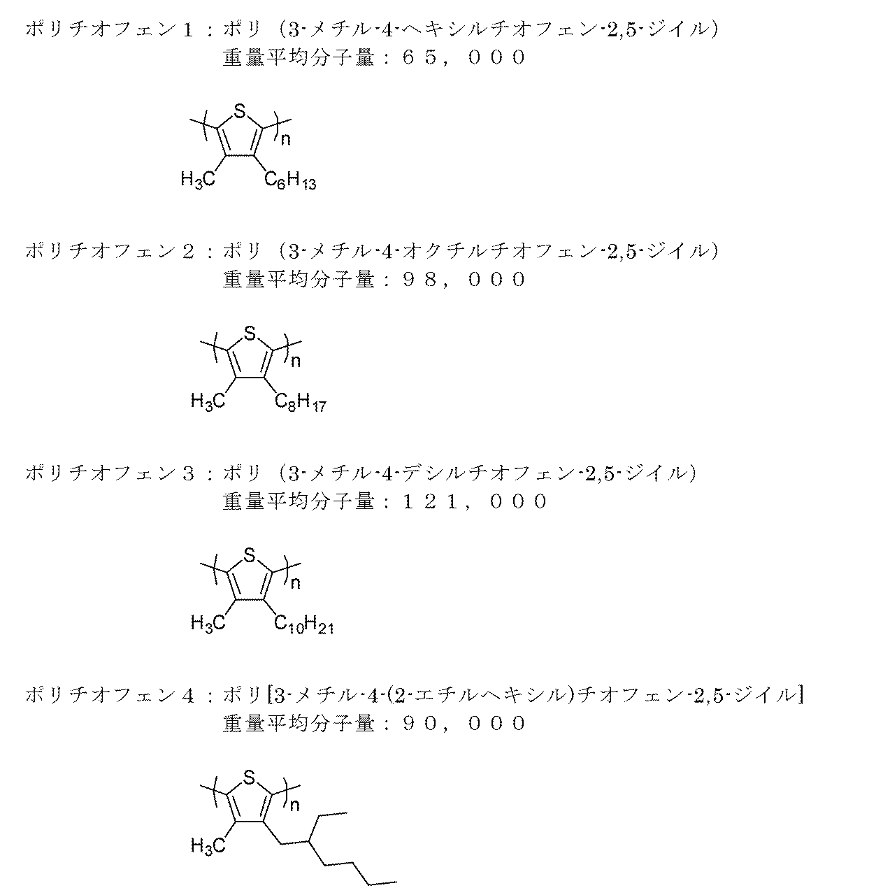
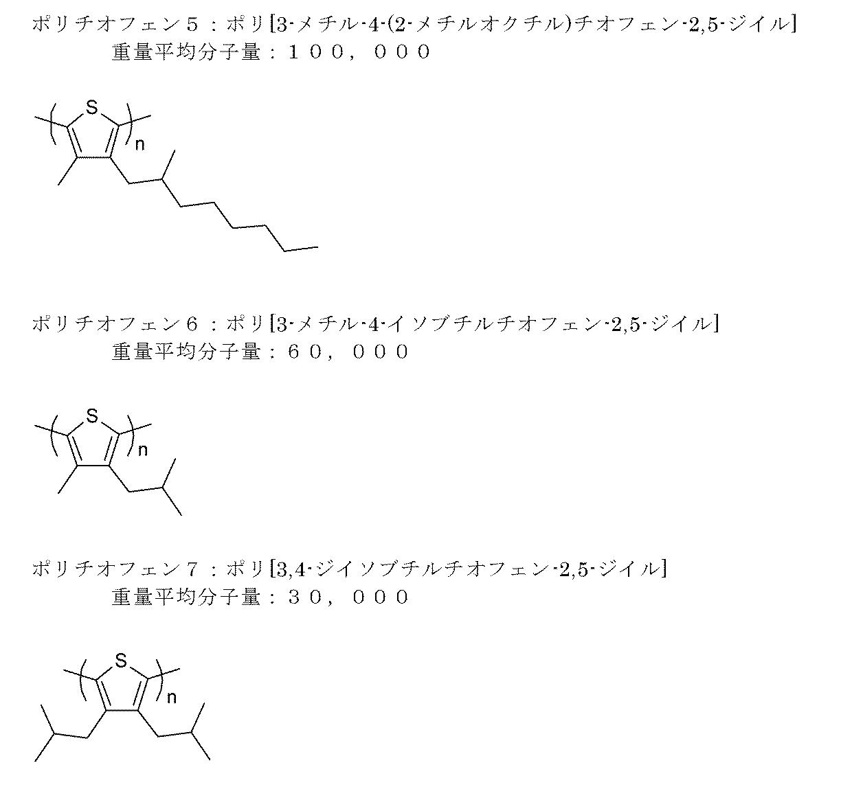

上記ポリチオフェン1~3はAmericanDyeSource社製、ポリチオフェン11~13はアルドリッチ社製の市販品を用いた。
上記ポリチオフェン4、5~7、14は、以下の手順により合成した。
1.ポリチオフェン4の合成
(1)3-メチル-4-(2-エチルヘキシル)チオフェン(原料モノマーA)の合成
窒素気流下、3-メチル-4-ブロモチオフェン 3g(17mmol)を脱水THF 20mLに溶解、0℃に冷却した。その溶液に2-エチルヘキシルマグネシウムブロミド(1M ジエチルエーテル溶液) 18mL(18mmol)を滴下し、滴下終了後、6時間加熱還流した。反応溶液を放冷却後、水、10%塩酸水溶液を加えて有機層を分離し、有機層を水、塩水で洗浄して硫酸マグネシウムで乾燥させた。溶液を濃縮後、シリカゲルカラムクロマトグラフ(ヘキサン100%)で精製することにより、無色の原料モノマーAを1.3g(収率36%)得た。得られた化合物は1H-NMRにより、3-メチル-4-(2-エチルヘキシル)チオフェンであることを確認した。
(2)ポリチオフェン4の合成
窒素気流下、塩化鉄(III) 0.82g(5.06mmol)をクロロホルム 10mLに溶解させた。その溶液に、上記で合成した原料モノマーA 0.27g(1.27mmol)を滴下して室温にて2時間撹拌し、水・メタノールを加えて反応を停止した。生じた黒色沈殿をクロロホルム100mLに再溶解した後、さらに水100mLを加えて撹拌することで金属不純物の洗浄を行った。クロロホルム層を濃縮し、アセトンを加えて赤色沈殿を得た。この沈殿をアセトン:メタノール=1:1(体積比)溶媒でソックスレー洗浄することにより、ポリチオフェン4を得た。得られた化合物は1H-NMRにより、上記に示す構造のポリチオフェン4であることを確認した。
(1)3-メチル-4-(2-エチルヘキシル)チオフェン(原料モノマーA)の合成
窒素気流下、3-メチル-4-ブロモチオフェン 3g(17mmol)を脱水THF 20mLに溶解、0℃に冷却した。その溶液に2-エチルヘキシルマグネシウムブロミド(1M ジエチルエーテル溶液) 18mL(18mmol)を滴下し、滴下終了後、6時間加熱還流した。反応溶液を放冷却後、水、10%塩酸水溶液を加えて有機層を分離し、有機層を水、塩水で洗浄して硫酸マグネシウムで乾燥させた。溶液を濃縮後、シリカゲルカラムクロマトグラフ(ヘキサン100%)で精製することにより、無色の原料モノマーAを1.3g(収率36%)得た。得られた化合物は1H-NMRにより、3-メチル-4-(2-エチルヘキシル)チオフェンであることを確認した。
(2)ポリチオフェン4の合成
窒素気流下、塩化鉄(III) 0.82g(5.06mmol)をクロロホルム 10mLに溶解させた。その溶液に、上記で合成した原料モノマーA 0.27g(1.27mmol)を滴下して室温にて2時間撹拌し、水・メタノールを加えて反応を停止した。生じた黒色沈殿をクロロホルム100mLに再溶解した後、さらに水100mLを加えて撹拌することで金属不純物の洗浄を行った。クロロホルム層を濃縮し、アセトンを加えて赤色沈殿を得た。この沈殿をアセトン:メタノール=1:1(体積比)溶媒でソックスレー洗浄することにより、ポリチオフェン4を得た。得られた化合物は1H-NMRにより、上記に示す構造のポリチオフェン4であることを確認した。
2.ポリチオフェン5の合成
特開2000-264957号公報に記載された方法に従って合成した。
特開2000-264957号公報に記載された方法に従って合成した。
3.ポリチオフェン6の合成
(1)3-メチル-4-イソブチルチオフェン(原料モノマーB)の合成
原料モノマーAの合成において、原料として2-エチルヘキシルマグネシウムブロミドに代えて、等モルのイソブチルマグネシウムブロミド(1M THF溶液)を用いた以外は、上記原料モノマーAの合成と同様にして、原料モノマーBを合成した。得られた化合物は1H-NMRにより、3-メチル-4-イソブチルチオフェンであることを確認した。
(2)ポリチオフェン6の合成
ポリチオフェン4の合成において、原料として原料モノマーAに代えて、等モルの原料モノマーBを用いた以外は、上記ポリチオフェン4の合成と同様にして、ポリチオフェン6を合成した。1H-NMRによって上記に示す構造のポリチオフェン6であることを確認した。
(1)3-メチル-4-イソブチルチオフェン(原料モノマーB)の合成
原料モノマーAの合成において、原料として2-エチルヘキシルマグネシウムブロミドに代えて、等モルのイソブチルマグネシウムブロミド(1M THF溶液)を用いた以外は、上記原料モノマーAの合成と同様にして、原料モノマーBを合成した。得られた化合物は1H-NMRにより、3-メチル-4-イソブチルチオフェンであることを確認した。
(2)ポリチオフェン6の合成
ポリチオフェン4の合成において、原料として原料モノマーAに代えて、等モルの原料モノマーBを用いた以外は、上記ポリチオフェン4の合成と同様にして、ポリチオフェン6を合成した。1H-NMRによって上記に示す構造のポリチオフェン6であることを確認した。
4.ポリチオフェン7の合成
(1)3,4-ジイソブチルチオフェン(原料モノマーC)の合成
窒素気流下、3、4-ジブロモチオフェン 2.45g(10mmol)を脱水THF 20mLに溶解、0℃に冷却した。その溶液にイソブチルマグネシウムブロミド(1M THF溶液) 22mL(22mmol)を滴下し、滴下終了後、2時間加熱還流した。反応溶液を放冷却後、水、10%塩酸水溶液を加えて有機層を分離し、有機層を水、塩水で洗浄して硫酸マグネシウムで乾燥させた。溶液を濃縮後、シリカゲルカラムクロマトグラフ(ヘキサン100%)で精製することにより、無色の原料モノマーCを0.6g(収率30%)得た。得られた化合物は1H-NMRにより、3,4-ジイソブチルチオフェンであることを確認した。
(2)ポリチオフェン7の合成
窒素気流下、塩化鉄(III) 0.82g(5.06mmol)をクロロホルム10mLに溶解させた。その溶液に、上記で合成した原料モノマーC 0.25g(1.27mmol)を滴下して室温にて2時間撹拌し、水・メタノールを加えて反応を停止した。生じた黒色沈殿物をクロロホルム100mLに再溶解した後、さらに水100mLを加えて撹拌することで金属不純物の洗浄を行った。クロロホルム層を濃縮し、アセトンを加えて沈殿を得た。この沈殿をアセトン:メタノール=1:1(体積比)溶媒でソックスレー洗浄することにより、ポリチオフェン7を得た。得られた化合物は1H-NMRにより、上記に示す構造のポリチオフェン7であることを確認した。
(1)3,4-ジイソブチルチオフェン(原料モノマーC)の合成
窒素気流下、3、4-ジブロモチオフェン 2.45g(10mmol)を脱水THF 20mLに溶解、0℃に冷却した。その溶液にイソブチルマグネシウムブロミド(1M THF溶液) 22mL(22mmol)を滴下し、滴下終了後、2時間加熱還流した。反応溶液を放冷却後、水、10%塩酸水溶液を加えて有機層を分離し、有機層を水、塩水で洗浄して硫酸マグネシウムで乾燥させた。溶液を濃縮後、シリカゲルカラムクロマトグラフ(ヘキサン100%)で精製することにより、無色の原料モノマーCを0.6g(収率30%)得た。得られた化合物は1H-NMRにより、3,4-ジイソブチルチオフェンであることを確認した。
(2)ポリチオフェン7の合成
窒素気流下、塩化鉄(III) 0.82g(5.06mmol)をクロロホルム10mLに溶解させた。その溶液に、上記で合成した原料モノマーC 0.25g(1.27mmol)を滴下して室温にて2時間撹拌し、水・メタノールを加えて反応を停止した。生じた黒色沈殿物をクロロホルム100mLに再溶解した後、さらに水100mLを加えて撹拌することで金属不純物の洗浄を行った。クロロホルム層を濃縮し、アセトンを加えて沈殿を得た。この沈殿をアセトン:メタノール=1:1(体積比)溶媒でソックスレー洗浄することにより、ポリチオフェン7を得た。得られた化合物は1H-NMRにより、上記に示す構造のポリチオフェン7であることを確認した。
5.ポリチオフェン14の合成
(1)3-(2-エチルヘキシル)チオフェン(原料モノマーD)の合成
窒素気流下、3-ブロモチオフェン 3.27g(20mmol)を脱水THF 20mLに溶解、0℃に冷却した。その溶液に2-エチルヘキシルマグネシウムブロミド(1M ジエチルエーテル溶液) 24mL(24mmol)を滴下し、滴下終了後、3時間加熱還流した。反応溶液を放冷却後、水、10%塩酸水溶液を加えて有機層を分離し、有機層を水、塩水で洗浄して硫酸マグネシウムで乾燥させた。溶液を濃縮後、シリカゲルカラムクロマトグラフ(ヘキサン100%)で精製することにより、無色の原料モノマーDを2.6g(収率66%)得た。得られた化合物は1H-NMRにより、3-(2-エチルヘキシル)チオフェンであることを確認した。
(2)ポリチオフェン14の合成
窒素気流下、塩化鉄(III) 0.82g(5.06mmol)をクロロホルム10mLに溶解させた。その溶液に、上記で合成した原料モノマーD 0.28g(1.27mmol)を滴下して室温にて2時間撹拌し、水・メタノールを加えて反応を停止した。生じた黒色沈殿物をクロロホルム100mLに再溶解した後、さらに水100mLを加えて撹拌することで金属不純物の洗浄を行った。クロロホルム層を濃縮し、アセトンを加えて沈殿を得た。この沈殿をアセトン:メタノール=1:1(体積比)溶媒でソックスレー洗浄することにより、ポリチオフェン14を得た。得られた化合物は1H-NMRにより、上記に示す構造のポリチオフェン14であることを確認した。
(1)3-(2-エチルヘキシル)チオフェン(原料モノマーD)の合成
窒素気流下、3-ブロモチオフェン 3.27g(20mmol)を脱水THF 20mLに溶解、0℃に冷却した。その溶液に2-エチルヘキシルマグネシウムブロミド(1M ジエチルエーテル溶液) 24mL(24mmol)を滴下し、滴下終了後、3時間加熱還流した。反応溶液を放冷却後、水、10%塩酸水溶液を加えて有機層を分離し、有機層を水、塩水で洗浄して硫酸マグネシウムで乾燥させた。溶液を濃縮後、シリカゲルカラムクロマトグラフ(ヘキサン100%)で精製することにより、無色の原料モノマーDを2.6g(収率66%)得た。得られた化合物は1H-NMRにより、3-(2-エチルヘキシル)チオフェンであることを確認した。
(2)ポリチオフェン14の合成
窒素気流下、塩化鉄(III) 0.82g(5.06mmol)をクロロホルム10mLに溶解させた。その溶液に、上記で合成した原料モノマーD 0.28g(1.27mmol)を滴下して室温にて2時間撹拌し、水・メタノールを加えて反応を停止した。生じた黒色沈殿物をクロロホルム100mLに再溶解した後、さらに水100mLを加えて撹拌することで金属不純物の洗浄を行った。クロロホルム層を濃縮し、アセトンを加えて沈殿を得た。この沈殿をアセトン:メタノール=1:1(体積比)溶媒でソックスレー洗浄することにより、ポリチオフェン14を得た。得られた化合物は1H-NMRにより、上記に示す構造のポリチオフェン14であることを確認した。
ポリチオフェンの分子量は、GPC(ゲル浸透クロマトグラフ)にて行った。各試料にo―ジクロロベンゼンを加えて145℃で溶解し、1.0μmの焼結フィルターでろ過して0.15wv%の試料溶液を調製して測定に用いた。測定は、装置:「Alliance GPC2000(Waters社製)」、カラム:TSKgel GMH6-HT×2+TSKgel GMH6-HTL×2(いずれも7.5mmI.D.×30cm、東ソー社製)、カラム温度:140℃、検出器:示差屈折率計、移動相:o-ジクロロベンゼンの構成・条件にて行い、平均分子量を求めた。分子量の構成は標準ポリスチレンを用いて行った。
また、上記ポリチオフェン1~14のイオン化ポテンシャルを、下記の方法により測定した。
[ポリチオフェン膜の作製]
ポリチオフェン 10mgに、THF-キシレン(7:3)溶液を1mL加えて、超音波洗浄器「US-2」(井内盛栄堂(株)製、出力120W、間接照射)を用いて溶解させた。一方、基板として、1.1mmの厚み、40mm×50mmのガラス基板をアセトン中で超音波洗浄した後、10分間UV-オゾン処理を行った。ポリチオフェンのTHF-キシレン溶液をこのガラス基板上にスピンコート(2000rpm、30秒間)した後、室温乾燥することでポリチオフェン膜を作製した。得られたポリチオフェン膜のイオン化ポテンシャルを、下記の手法で測定・評価した。
[イオン化ポテンシャルの測定]
ポリチオフェンのイオン化ポテンシャルは、光電子分光装置「AC-2」(理研計器(株)製)を用い、大気中にて光電子分光によって測定した。イオン化ポテンシャルの値が正に大きいほど、ポリチオフェン高分子の主鎖の共役系が切断される状態を示し、よって高分子主鎖のねじれが大きい。
[ポリチオフェン膜の作製]
ポリチオフェン 10mgに、THF-キシレン(7:3)溶液を1mL加えて、超音波洗浄器「US-2」(井内盛栄堂(株)製、出力120W、間接照射)を用いて溶解させた。一方、基板として、1.1mmの厚み、40mm×50mmのガラス基板をアセトン中で超音波洗浄した後、10分間UV-オゾン処理を行った。ポリチオフェンのTHF-キシレン溶液をこのガラス基板上にスピンコート(2000rpm、30秒間)した後、室温乾燥することでポリチオフェン膜を作製した。得られたポリチオフェン膜のイオン化ポテンシャルを、下記の手法で測定・評価した。
[イオン化ポテンシャルの測定]
ポリチオフェンのイオン化ポテンシャルは、光電子分光装置「AC-2」(理研計器(株)製)を用い、大気中にて光電子分光によって測定した。イオン化ポテンシャルの値が正に大きいほど、ポリチオフェン高分子の主鎖の共役系が切断される状態を示し、よって高分子主鎖のねじれが大きい。
実施例1-1
単層カーボンナノチューブとしてASP-100F(Hanwha nanotech社製、純度95%)10mg、及び25mgのポリチオフェン1に、o-ジクロロベンゼン10mLを加えて、メカニカルな攪拌装置で20分間攪拌した。その後、超音波洗浄機「US-2」(井内盛栄堂(株)製、出力120W、間接照射)を用いて、30℃で40分間超音波分散することによって、熱電変換材料のo-ジクロロベンゼン溶液を作製した。一方、基板として、1.1mmの厚み、40mm×50mmのガラス基板をアセトン中で超音波洗浄した後、10分間UV-オゾン処理を行った。上記熱電変換材料のo-ジクロロベンゼン溶液をこのガラス基板上にスピンコート(1500rpm、30秒間)した後、室温真空条件で3時間乾燥することで、厚さ約50nmの熱電変換層を形成した。
得られた熱電変換層の導電率、CNT分散性を、下記の手法で測定・評価した。結果を表1に示す。
単層カーボンナノチューブとしてASP-100F(Hanwha nanotech社製、純度95%)10mg、及び25mgのポリチオフェン1に、o-ジクロロベンゼン10mLを加えて、メカニカルな攪拌装置で20分間攪拌した。その後、超音波洗浄機「US-2」(井内盛栄堂(株)製、出力120W、間接照射)を用いて、30℃で40分間超音波分散することによって、熱電変換材料のo-ジクロロベンゼン溶液を作製した。一方、基板として、1.1mmの厚み、40mm×50mmのガラス基板をアセトン中で超音波洗浄した後、10分間UV-オゾン処理を行った。上記熱電変換材料のo-ジクロロベンゼン溶液をこのガラス基板上にスピンコート(1500rpm、30秒間)した後、室温真空条件で3時間乾燥することで、厚さ約50nmの熱電変換層を形成した。
得られた熱電変換層の導電率、CNT分散性を、下記の手法で測定・評価した。結果を表1に示す。
[導電率の測定]
形成した熱電変換層の導電率は、「高抵抗率計:ハイレスタUP」または「低抵抗率計:ロレスタGP」(いずれも(株)三菱化学アナリテック製)を用い表面抵抗率(単位:Ω/□)を測定し、触針型膜厚計により膜厚(単位:cm)を測定し、下記式より導電率(S/cm)を算出した。
(導電率)=1/((表面抵抗)×(膜厚))
形成した熱電変換層の導電率は、「高抵抗率計:ハイレスタUP」または「低抵抗率計:ロレスタGP」(いずれも(株)三菱化学アナリテック製)を用い表面抵抗率(単位:Ω/□)を測定し、触針型膜厚計により膜厚(単位:cm)を測定し、下記式より導電率(S/cm)を算出した。
(導電率)=1/((表面抵抗)×(膜厚))
[CNT分散性]
CNT分散性は目視により下記の3段階の基準で評価した。
1:CNTの分散に要する時間が5分より短い
2:CNTの分散に要する時間が5分以上、15分より短い
3:CNTの分散に要する時間が15分以上
CNT分散性は目視により下記の3段階の基準で評価した。
1:CNTの分散に要する時間が5分より短い
2:CNTの分散に要する時間が5分以上、15分より短い
3:CNTの分散に要する時間が15分以上
実施例1-2~1-7
実施例1-1において、ポリチオフェンの種類を表1に示すように変更した以外は実施例1-1と同様にして、熱電変換層を形成し、評価した。結果を表1に示す。
実施例1-1において、ポリチオフェンの種類を表1に示すように変更した以外は実施例1-1と同様にして、熱電変換層を形成し、評価した。結果を表1に示す。
実施例1-8
実施例1-1において、単層カーボンナノチューブとしてASP-100F(Hanwha nanotech社製、純度95%)0.5mg、及び34.5mgのポリチオフェン1を用いた以外は、実施例1-1と同様にして熱電変換層を形成し、評価した。
実施例1-1において、単層カーボンナノチューブとしてASP-100F(Hanwha nanotech社製、純度95%)0.5mg、及び34.5mgのポリチオフェン1を用いた以外は、実施例1-1と同様にして熱電変換層を形成し、評価した。
比較例1-1~1-4
実施例1-1において、ポリチオフェンの種類を表1に示すように変更した以外は実施例1-1と同様にして、熱電変換層を形成し、評価した。結果を表1に示す。
実施例1-1において、ポリチオフェンの種類を表1に示すように変更した以外は実施例1-1と同様にして、熱電変換層を形成し、評価した。結果を表1に示す。
比較例1-5
実施例1-1において、単層カーボンナノチューブとしてASP-100F(Hanwha nanotech社製、純度95%)0.5mg、及び34.5mgのポリチオフェン11を用いた以外は、実施例1-1と同様にして熱電変換層を形成し、評価した。
実施例1-1において、単層カーボンナノチューブとしてASP-100F(Hanwha nanotech社製、純度95%)0.5mg、及び34.5mgのポリチオフェン11を用いた以外は、実施例1-1と同様にして熱電変換層を形成し、評価した。
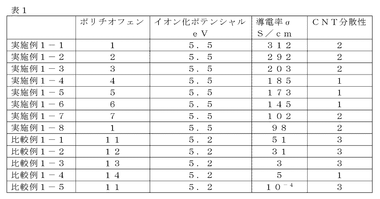
表1から明らかなように、チオフェン環の3位及び4位がともにアルキル基で置換されているポリチオフェン重合体、及びCNTを含有する熱電変換材料を用いた実施例1-1~1-8は、ポリチオフェン重合体の主鎖のねじれが大きく、高い導電率と、良好なCNT分散性を示し、CNTの欠陥も少なかった。さらに、熱電変換材料の全固形分中のCNT含有量が2~60質量%の範囲であり、かつポリチオフェン重合体の含有量が20~80質量%の範囲である実施例1-1~1-7は、実施例1-8に比べて、高い導電率を示した。また、チオフェン環の置換基の一方が分岐アルキル基であるポリチオフェンを用いた実施例1-4~1-6では、CNT分散性が一層向上した。
これに対し、チオフェン環の3位及び4位のいずれか一方が水素原子であるポリチオフェンを用いた比較例1-1~1-5では、ポリマー主鎖のねじれが小さく、導電率が大きく低下した。さらに、熱電変換材料の全固形分中のCNT含有量が2質量%未満で、かつポリチオフェン重合体の含有量が80質量%を超える比較例1-5は、導電率と分散性が著しく低下した。
これに対し、チオフェン環の3位及び4位のいずれか一方が水素原子であるポリチオフェンを用いた比較例1-1~1-5では、ポリマー主鎖のねじれが小さく、導電率が大きく低下した。さらに、熱電変換材料の全固形分中のCNT含有量が2質量%未満で、かつポリチオフェン重合体の含有量が80質量%を超える比較例1-5は、導電率と分散性が著しく低下した。
実施例2-1
厚さ300μmのニトフロンNo.901UL(日東電工社製)と両面粘着フイルムを用い、ガラス基板上に型枠を作製した。型枠内に実施例1-1と同様に作製した熱電変換材料のo-ジクロロベンゼン溶液を流し込み、室温下で乾燥させたのち、温度80℃のホットプレート上で10分間アニール処理を行い、該型枠を剥離することで、厚さ2.0μmの熱電変換層を成膜し、熱電変換素子を作製した。
得られた熱電変換素子の導電率、熱電特性、成膜性を下記の手法で測定・評価した。結果を表2に示す。
厚さ300μmのニトフロンNo.901UL(日東電工社製)と両面粘着フイルムを用い、ガラス基板上に型枠を作製した。型枠内に実施例1-1と同様に作製した熱電変換材料のo-ジクロロベンゼン溶液を流し込み、室温下で乾燥させたのち、温度80℃のホットプレート上で10分間アニール処理を行い、該型枠を剥離することで、厚さ2.0μmの熱電変換層を成膜し、熱電変換素子を作製した。
得られた熱電変換素子の導電率、熱電特性、成膜性を下記の手法で測定・評価した。結果を表2に示す。
[導電率、熱電特性の評価]
熱電特性測定装置MODEL RZ2001i(オザワ科学社製)を用い、温度100℃の大気雰囲気で測定を行い、ゼーベック係数(V/K)と導電率(S/cm)を測定した。得られたゼーベック係数と導電率から、熱電特性としてPower Factor (PF値)を、下記式より算出した。
PF=(ゼーベック係数)2×(導電率)
熱電特性測定装置MODEL RZ2001i(オザワ科学社製)を用い、温度100℃の大気雰囲気で測定を行い、ゼーベック係数(V/K)と導電率(S/cm)を測定した。得られたゼーベック係数と導電率から、熱電特性としてPower Factor (PF値)を、下記式より算出した。
PF=(ゼーベック係数)2×(導電率)
[成膜性の評価]
成膜性は熱電変換層を目視により観察し、下記の2段階の基準で評価した。
1:凝集物がほぼ確認されず、成膜性が良好。
2:凝集物が少し確認され、成膜性が低下。
成膜性は熱電変換層を目視により観察し、下記の2段階の基準で評価した。
1:凝集物がほぼ確認されず、成膜性が良好。
2:凝集物が少し確認され、成膜性が低下。
実施例2-2~2-7
実施例2-1において、熱電変換材料として実施例1-2~1-7と同様に作製した熱電変換材料のo-ジクロロベンゼン溶液を用いた以外は、実施例2-1と同様にして、熱電変換素子を作製し、評価した。
実施例2-1において、熱電変換材料として実施例1-2~1-7と同様に作製した熱電変換材料のo-ジクロロベンゼン溶液を用いた以外は、実施例2-1と同様にして、熱電変換素子を作製し、評価した。
比較例2-1~2-4
実施例2-1において、熱電変換材料として比較例1-1~1-4と同様に作製した熱電変換材料のo-ジクロロベンゼン溶液を用いた以外は、実施例2-1と同様にして、熱電変換素子を作製し、評価した。
実施例2-1において、熱電変換材料として比較例1-1~1-4と同様に作製した熱電変換材料のo-ジクロロベンゼン溶液を用いた以外は、実施例2-1と同様にして、熱電変換素子を作製し、評価した。
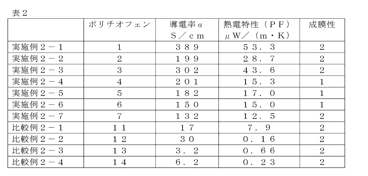
表2から明らかなように、チオフェン環の3位及び4位がともにアルキル基で置換されているポリチオフェン重合体、及びCNTを含有する熱電変換材料を用いた実施例2-1~2-7では、高い導電率と熱電特性(PF値)を示し、成膜性も優れていた。特に、チオフェン環の置換基の一方が分岐アルキル基であるポリチオフェンを用いた実施例2-4~2-6では、成膜性が一層向上した。
これに対し、チオフェン環の3位及び4位のいずれか一方が水素原子であるポリチオフェンを用いた比較例2-1~2-4では、導電率、熱電特性がともに低かった。
これに対し、チオフェン環の3位及び4位のいずれか一方が水素原子であるポリチオフェンを用いた比較例2-1~2-4では、導電率、熱電特性がともに低かった。
実施例3-1
1.カーボンナノチューブ分散ペーストの作製
ポリチオフェン2(AmericanDyeSource社製)720mgに、o-ジクロロベンゼン40mlを加えて、超音波洗浄機「US-2」(井内盛栄堂(株)製、出力120W、間接照射)を用い、40℃で10分間の条件で、ポリチオフェン溶液3-1を作製した。
次に、溶液3-1に単層カーボンナノチューブとしてASP-100F(Hanwha nanotech社製、純度95%)960mgを加え、超音波ホモジナイザーVC-750(SONICS&MATERIALS.Inc製、テーパーマイクロチップ(プローブ径6.5mm)使用、出力50W、直接照射、Duty比50%)を用いて、30℃で30分間超音波分散し、さらに、超音波洗浄機「US-2」(井内盛栄堂(株)製、出力120W、間接照射)を用いて、30℃で60分間超音波分散することによって、カーボンナノチューブ分散液3-1を作製した。
次に、分散液3-1に非共役高分子として重合度2,000のポリスチレン(和光純薬製)1.68g添加し、50℃の温浴中にて溶解させたのち、自公転式攪拌装置ARE-250(シンキー製)で回転数2000rpm、攪拌時間15分で攪拌することで、カーボンナノチューブ分散ペースト3-1を作製した。このペーストの固形分中のCNT含有率は28.6質量%、ポリチオフェン含有率は21.4質量%であった。分散ペースト3-1のCNT分散性を評価した。
1.カーボンナノチューブ分散ペーストの作製
ポリチオフェン2(AmericanDyeSource社製)720mgに、o-ジクロロベンゼン40mlを加えて、超音波洗浄機「US-2」(井内盛栄堂(株)製、出力120W、間接照射)を用い、40℃で10分間の条件で、ポリチオフェン溶液3-1を作製した。
次に、溶液3-1に単層カーボンナノチューブとしてASP-100F(Hanwha nanotech社製、純度95%)960mgを加え、超音波ホモジナイザーVC-750(SONICS&MATERIALS.Inc製、テーパーマイクロチップ(プローブ径6.5mm)使用、出力50W、直接照射、Duty比50%)を用いて、30℃で30分間超音波分散し、さらに、超音波洗浄機「US-2」(井内盛栄堂(株)製、出力120W、間接照射)を用いて、30℃で60分間超音波分散することによって、カーボンナノチューブ分散液3-1を作製した。
次に、分散液3-1に非共役高分子として重合度2,000のポリスチレン(和光純薬製)1.68g添加し、50℃の温浴中にて溶解させたのち、自公転式攪拌装置ARE-250(シンキー製)で回転数2000rpm、攪拌時間15分で攪拌することで、カーボンナノチューブ分散ペースト3-1を作製した。このペーストの固形分中のCNT含有率は28.6質量%、ポリチオフェン含有率は21.4質量%であった。分散ペースト3-1のCNT分散性を評価した。
2.熱電変換層の作製
上記で調製したカーボンナノチューブ分散ペースト3-1を基板上に成膜して、熱電変換層を形成した。
詳細には、イソプロピルアルコール中で超音波洗浄した後、10分間UV-オゾン処理を行った厚み1.1mmのガラス基板上に、レーザー加工で形成した開口部13×13mmを有し、かつ厚み2mmのメタルマスクをかぶせた。次に、開口部に上記で調製したカーボンナノチューブ分散ペースト3-1を注入したのち、メタルマスクを取り外し、次いでガラス基板を80℃のホットプレート上で加熱乾燥させて、熱電変換層3-1を作製し、その成膜性、導電率、及び熱電特性を評価した。
上記で調製したカーボンナノチューブ分散ペースト3-1を基板上に成膜して、熱電変換層を形成した。
詳細には、イソプロピルアルコール中で超音波洗浄した後、10分間UV-オゾン処理を行った厚み1.1mmのガラス基板上に、レーザー加工で形成した開口部13×13mmを有し、かつ厚み2mmのメタルマスクをかぶせた。次に、開口部に上記で調製したカーボンナノチューブ分散ペースト3-1を注入したのち、メタルマスクを取り外し、次いでガラス基板を80℃のホットプレート上で加熱乾燥させて、熱電変換層3-1を作製し、その成膜性、導電率、及び熱電特性を評価した。
3.熱電変換素子の作製
上記で調製したカーボンナノチューブ分散ペースト3-1を用いて、図3に示す熱電変換素子を作製した。
詳細には、イソプロピルアルコール中で超音波洗浄した後、大きさ40×50mm、厚み1.1mのガラス基板(32)上に、エッチングにより形成した開口部20×20mmのメタルマスクを用いて、イオンプレーティング法によりクロムを100nm、次に金を200nm積層成膜(30及び31)することにより、電極1(33)を形成した。
次に、レーザー加工で形成した開口部13×13mmを有し、かつ厚み2mmのメタルマスクを用いて、上記で調製したカーボンナノチューブ分散ペースト3-1を注入し、次いでガラス基板を80℃のホットプレート上で加熱乾燥させることで、電極1上に熱電変換層3-1(34)を形成した。
次に、導電性ペーストドータイトD-550(藤倉化成製、銀ペースト)をスクリーン印刷法により塗布して、熱電変換層3-1上に電極2(35)を成膜し、熱電変換素子3-1(3)を作製し、その熱起電力を評価した。
上記で調製したカーボンナノチューブ分散ペースト3-1を用いて、図3に示す熱電変換素子を作製した。
詳細には、イソプロピルアルコール中で超音波洗浄した後、大きさ40×50mm、厚み1.1mのガラス基板(32)上に、エッチングにより形成した開口部20×20mmのメタルマスクを用いて、イオンプレーティング法によりクロムを100nm、次に金を200nm積層成膜(30及び31)することにより、電極1(33)を形成した。
次に、レーザー加工で形成した開口部13×13mmを有し、かつ厚み2mmのメタルマスクを用いて、上記で調製したカーボンナノチューブ分散ペースト3-1を注入し、次いでガラス基板を80℃のホットプレート上で加熱乾燥させることで、電極1上に熱電変換層3-1(34)を形成した。
次に、導電性ペーストドータイトD-550(藤倉化成製、銀ペースト)をスクリーン印刷法により塗布して、熱電変換層3-1上に電極2(35)を成膜し、熱電変換素子3-1(3)を作製し、その熱起電力を評価した。
4.試験方法
[CNT分散性]
CNT分散性はカーボンナノチューブ分散ペーストをスライドガラスに滴下し、カバーガラスをのせたのち、目視により観察し、および下記の4段階の基準で評価した。
1:黒色の凝集物が観測されなかった。
2:大きさ0.5mm未満の黒色の凝集物が観測された。
3:大きさ0.5mm以上、1mm未満の黒色の凝集物が観測された。
4:凝集物が基準3を超える量観察された。
[CNT分散性]
CNT分散性はカーボンナノチューブ分散ペーストをスライドガラスに滴下し、カバーガラスをのせたのち、目視により観察し、および下記の4段階の基準で評価した。
1:黒色の凝集物が観測されなかった。
2:大きさ0.5mm未満の黒色の凝集物が観測された。
3:大きさ0.5mm以上、1mm未満の黒色の凝集物が観測された。
4:凝集物が基準3を超える量観察された。
[成膜性]
成膜性は目視により下記の3段階の基準で評価した。
1:メタルマスクの開口部にくらべ、熱電変換層の大きさが1.5倍以下
2:メタルマスクの開口部にくらべ、熱電変換層の大きさが1.5倍より大きく、2.0
倍以下
3:メタルマスクの開口部にくらべ、熱電変換層の大きさが2.0倍より大きい
成膜性は目視により下記の3段階の基準で評価した。
1:メタルマスクの開口部にくらべ、熱電変換層の大きさが1.5倍以下
2:メタルマスクの開口部にくらべ、熱電変換層の大きさが1.5倍より大きく、2.0
倍以下
3:メタルマスクの開口部にくらべ、熱電変換層の大きさが2.0倍より大きい
[導電率]
実施例2-1と同様にして評価した。
実施例2-1と同様にして評価した。
[熱電特性(PF)]
実施例2-1と同様にして算出したPower Factor(PF値)をもとに、下記比較例3-1に対する相対値で評価した。
実施例2-1と同様にして算出したPower Factor(PF値)をもとに、下記比較例3-1に対する相対値で評価した。
[熱起電力]
熱電変換素子の熱起電力は、熱電変換素子のガラス基板を表面温度80℃のホットプレートで加熱した際に、電極1-電極2間で生じる電圧差を、デジタルマルチメーターR6581(アドバンテスト社製)で測定した。
測定した値をもとに、下記比較例3-1に対する相対値で評価した。
熱電変換素子の熱起電力は、熱電変換素子のガラス基板を表面温度80℃のホットプレートで加熱した際に、電極1-電極2間で生じる電圧差を、デジタルマルチメーターR6581(アドバンテスト社製)で測定した。
測定した値をもとに、下記比較例3-1に対する相対値で評価した。
実施例3-2、3-3
実施例3-1において、ポリチオフェン2を、同量のポリチオフェン4又は5に変更した以外は、実施例3-1と同様にして、熱電変換層及び熱電変換素子を作製し、その特性を評価した。
実施例3-1において、ポリチオフェン2を、同量のポリチオフェン4又は5に変更した以外は、実施例3-1と同様にして、熱電変換層及び熱電変換素子を作製し、その特性を評価した。
比較例3-1
実施例3-1において、ポリチオフェン2を、同量のポリチオフェン12に変更した以外は、実施例3-1と同様にして、比較用熱電変換層及び熱電変換素子を作製し、その特性を評価した。
実施例3-1において、ポリチオフェン2を、同量のポリチオフェン12に変更した以外は、実施例3-1と同様にして、比較用熱電変換層及び熱電変換素子を作製し、その特性を評価した。
評価結果を表3に示す。

表3から明らかなように、チオフェン環の3位及び4位がともにアルキル基で置換されているポリチオフェン重合体、及びCNT、非共役高分子を含有する熱電変換層を有する実施例3-1~3-3は、CNT分散性と成膜性に優れ、かつ導電率、熱電特性(PF)及び熱起電力にも優れていた。また、チオフェン環の置換基の一方が分岐アルキル基であるポリチオフェンを用いた実施例3-2、3-3では、CNT分散性がより一層向上した。
これに対し、チオフェン環の3位及び4位のいずれか一方が水素原子であるポリチオフェンを用いた比較例3-1では、導電率が低かった。
これに対し、チオフェン環の3位及び4位のいずれか一方が水素原子であるポリチオフェンを用いた比較例3-1では、導電率が低かった。
実施例4-1
360mgのポリチオフェン2に、o-ジクロロベンゼン30mlを加えて、超音波洗浄機「US-2」(井内盛栄堂(株)製、出力120W、間接照射)を用い、ポリチオフェン溶液4-1を作製した。
次に、溶液4-1に単層カーボンナノチューブとしてKH SWCNT HP(KH Chemicals社製、純度80%)480mgを加え、超音波ホモジナイザーVC-750(SONICS&MATERIALS.Inc製、テーパーマイクロチップ(プローブ径6.5mm)使用、出力50W、直接照射、Duty比50%)を用いて、30℃で30分間超音波分散することで、カーボンナノチューブ分散液4-1を作製した。
次に、分散液4-1に非共役高分子としてポリ(2-ビニルナフタレン)(重量平均分子量17.5万、Aldrich製)0.86g添加し、50℃の温浴中にて溶解させたのち、自公転式攪拌装置ARE-250(シンキー製)で回転数2200rpm、攪拌時間15分で攪拌することで、カーボンナノチューブ分散ペースト前駆体4-1を作製した。
さらに、前駆体4-1を、3本ロールミル分散機BR-100V(アイメックス社製)を用い、回転比1:1.7:2.9の条件で、15回切り返し、カーボンナノチューブ分散ペースト4-1を調製した。
このペーストの固形分中のCNT含有率は28.2質量%、ポリチオフェンの含有率は21.1質量%であった。分散ペースト4-1のCNT分散性を実施例3-1と同様に評価した。
360mgのポリチオフェン2に、o-ジクロロベンゼン30mlを加えて、超音波洗浄機「US-2」(井内盛栄堂(株)製、出力120W、間接照射)を用い、ポリチオフェン溶液4-1を作製した。
次に、溶液4-1に単層カーボンナノチューブとしてKH SWCNT HP(KH Chemicals社製、純度80%)480mgを加え、超音波ホモジナイザーVC-750(SONICS&MATERIALS.Inc製、テーパーマイクロチップ(プローブ径6.5mm)使用、出力50W、直接照射、Duty比50%)を用いて、30℃で30分間超音波分散することで、カーボンナノチューブ分散液4-1を作製した。
次に、分散液4-1に非共役高分子としてポリ(2-ビニルナフタレン)(重量平均分子量17.5万、Aldrich製)0.86g添加し、50℃の温浴中にて溶解させたのち、自公転式攪拌装置ARE-250(シンキー製)で回転数2200rpm、攪拌時間15分で攪拌することで、カーボンナノチューブ分散ペースト前駆体4-1を作製した。
さらに、前駆体4-1を、3本ロールミル分散機BR-100V(アイメックス社製)を用い、回転比1:1.7:2.9の条件で、15回切り返し、カーボンナノチューブ分散ペースト4-1を調製した。
このペーストの固形分中のCNT含有率は28.2質量%、ポリチオフェンの含有率は21.1質量%であった。分散ペースト4-1のCNT分散性を実施例3-1と同様に評価した。
実施例4-2
実施例4-1において、ポリチオフェン2のかわりに、同量のポリチオフェン4を用いた以外は、実施例4-1と同様にして、カーボンナノチューブ分散ペースト4-2を作製した。
実施例4-1において、ポリチオフェン2のかわりに、同量のポリチオフェン4を用いた以外は、実施例4-1と同様にして、カーボンナノチューブ分散ペースト4-2を作製した。
実施例4-3
実施例4-2において、ポリ(2-ビニルナフタレン)のかわりに、同量のPC-Z型ポリカーボネート(帝人化成株式会社製、製品名「パンライトTS-2020」)を用いた以外は実施例4-2と同様にして、カーボンナノチューブ分散ペースト4-3を作製した。
実施例4-2において、ポリ(2-ビニルナフタレン)のかわりに、同量のPC-Z型ポリカーボネート(帝人化成株式会社製、製品名「パンライトTS-2020」)を用いた以外は実施例4-2と同様にして、カーボンナノチューブ分散ペースト4-3を作製した。
実施例3-1において、カーボンナノチューブ分散ペースト3-1を、上記で作製した分散ペースト4-1~4-3の各ペーストに変更した以外は実施例3-1と同様にして、熱電変換層及び熱電変換素子を作製し、その特性を実施例3-1と同様に評価した。結果を表4に示す。
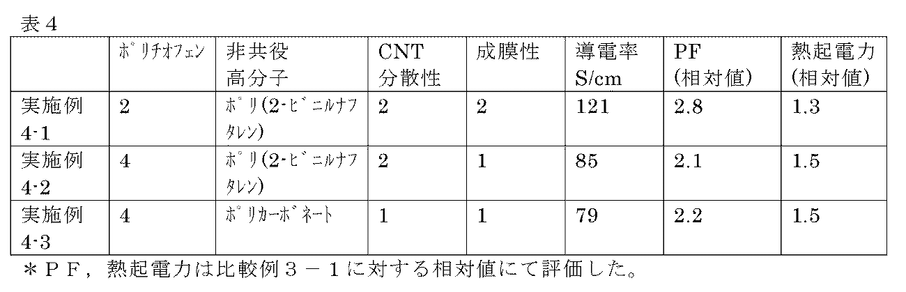
表4から明らかなように、チオフェン環の3位及び4位がともにアルキル基で置換されているポリチオフェン重合体、及びCNT、非共役高分子を含有する熱電変換層を有する実施例4-1~4-3は、CNT分散性と成膜性に優れ、かつ導電率、熱電特性(PF)及び熱起電力にも優れていた。また、チオフェン環の置換基の一方が分岐アルキル基であるポリチオフェンを用いた実施例4-2、4-3は、CNT分散性又は成膜性が一層向上した。
実施例5-1
基板として、下記で作製したポリエチレンテレフタレート(以下、PET)フィルムを用いて熱電変換素子を作製した。
基板として、下記で作製したポリエチレンテレフタレート(以下、PET)フィルムを用いて熱電変換素子を作製した。
1.支持体の作製
Geを触媒として重縮合したPET樹脂を含水率50ppm以下に乾燥させ、ヒーター温度を280~300℃に設定し、押し出し機内で溶融させた。溶融させたPET樹脂をダイ部より静電印加されたチルロール上に吐出させ、非結晶ベースを得た。得られた非結晶ベースをベース進行方向に3.3倍に延伸した後、幅方向に対して3.8倍に延伸し、厚さ188μmの支持体を得た。
Geを触媒として重縮合したPET樹脂を含水率50ppm以下に乾燥させ、ヒーター温度を280~300℃に設定し、押し出し機内で溶融させた。溶融させたPET樹脂をダイ部より静電印加されたチルロール上に吐出させ、非結晶ベースを得た。得られた非結晶ベースをベース進行方向に3.3倍に延伸した後、幅方向に対して3.8倍に延伸し、厚さ188μmの支持体を得た。
2.接着層の形成
得られた支持体の両面に対して730J/m2の条件でコロナ放電処理を行った後、この両面に下記組成の接着層用塗布液Aを塗布量4.4cm3/m2としてバーコート法により塗布した。そして、これを160℃で1分乾燥して接着層を形成することで、支持体の両面に接着層が形成された積層シート(導電体)を得た。
得られた支持体の両面に対して730J/m2の条件でコロナ放電処理を行った後、この両面に下記組成の接着層用塗布液Aを塗布量4.4cm3/m2としてバーコート法により塗布した。そして、これを160℃で1分乾燥して接着層を形成することで、支持体の両面に接着層が形成された積層シート(導電体)を得た。
-接着層用塗布液Aの組成-
・ウレタン樹脂バインダ 30.7質量部
(三井化学(株)製、オレスターUD350、固形分38質量%、ガラス転移温度33℃)
・アクリル樹脂バインダ 4.2質量部
(ダイセルファインケム(株)製AS563、固形分27.5質量%、ガラス転移温度47℃)
・架橋剤 5.8質量部
(日清紡(株)製、カルボジライトV-02-L2、固形分40質量%)
・添加剤(フィラー) 1.9質量部
(日本アエロジル(株)製、アエロジルOX-50、固形分10質量%)
・添加剤(フィラー) 0.8質量部
(日産化学(株)製,スノーテックスXL、固形分40質量%)
・添加剤(すべり剤) 1.9質量部
(中京油脂(株)製、セロゾール524、固形分30質量%)
・界面活性剤1 15.5質量部
(日本油脂(株)製、ラピゾールB-90、アニオン性1質量%)
・界面活性剤2 19.4質量部
(三洋化成工業(株)製、ナロアクティーCL-95、ノニオン性1質量%)
・純水 合計が1000質量部になるように添加
・ウレタン樹脂バインダ 30.7質量部
(三井化学(株)製、オレスターUD350、固形分38質量%、ガラス転移温度33℃)
・アクリル樹脂バインダ 4.2質量部
(ダイセルファインケム(株)製AS563、固形分27.5質量%、ガラス転移温度47℃)
・架橋剤 5.8質量部
(日清紡(株)製、カルボジライトV-02-L2、固形分40質量%)
・添加剤(フィラー) 1.9質量部
(日本アエロジル(株)製、アエロジルOX-50、固形分10質量%)
・添加剤(フィラー) 0.8質量部
(日産化学(株)製,スノーテックスXL、固形分40質量%)
・添加剤(すべり剤) 1.9質量部
(中京油脂(株)製、セロゾール524、固形分30質量%)
・界面活性剤1 15.5質量部
(日本油脂(株)製、ラピゾールB-90、アニオン性1質量%)
・界面活性剤2 19.4質量部
(三洋化成工業(株)製、ナロアクティーCL-95、ノニオン性1質量%)
・純水 合計が1000質量部になるように添加
3.カーボンナノチューブ分散ペーストの作製
実施例4-1において、ポリ(2-ビニルナフタレン)のかわりに同量の重合度2,000のポリスチレン(和光純薬製)を用いた以外は実施例4-1と同様にして、カーボンナノチューブ分散ペースト5-1を作製した。
実施例4-1において、ポリ(2-ビニルナフタレン)のかわりに同量の重合度2,000のポリスチレン(和光純薬製)を用いた以外は実施例4-1と同様にして、カーボンナノチューブ分散ペースト5-1を作製した。
4.熱電変換素子の作製
大きさ40×50mmの積層シート上に、エッチングにより形成した開口部20×20mmのメタルマスクを用いて、イオンプレーティング法によりクロムを100nm、次に金を200nm積層成膜することにより、電極1を形成した。
次に、レーザー加工で形成した開口部13×13mmを有し、かつ厚み2mmのメタルマスクを用いて、上記で調製したカーボンナノチューブ分散ペースト5-1を注入し、フィルム基板を80℃のホットプレート上で加熱乾燥させることで、電極1上に熱電変換層5-1を形成した。
次に、導電性ペーストドータイトD-550(藤倉化成製、銀ペースト)をスクリーン印刷法により塗布して、熱電変換層5-1上に電極2を成膜し、熱電変換素子5-1を作製した。
熱電変換素子のフィルム基板を表面温度80℃のホットプレートで加熱した際に、電極1-電極2間で生じる電圧差を、デジタルマルチメーターR6581(アドバンテスト社製)で測定したところ、電圧差が生じるのを確認した。
大きさ40×50mmの積層シート上に、エッチングにより形成した開口部20×20mmのメタルマスクを用いて、イオンプレーティング法によりクロムを100nm、次に金を200nm積層成膜することにより、電極1を形成した。
次に、レーザー加工で形成した開口部13×13mmを有し、かつ厚み2mmのメタルマスクを用いて、上記で調製したカーボンナノチューブ分散ペースト5-1を注入し、フィルム基板を80℃のホットプレート上で加熱乾燥させることで、電極1上に熱電変換層5-1を形成した。
次に、導電性ペーストドータイトD-550(藤倉化成製、銀ペースト)をスクリーン印刷法により塗布して、熱電変換層5-1上に電極2を成膜し、熱電変換素子5-1を作製した。
熱電変換素子のフィルム基板を表面温度80℃のホットプレートで加熱した際に、電極1-電極2間で生じる電圧差を、デジタルマルチメーターR6581(アドバンテスト社製)で測定したところ、電圧差が生じるのを確認した。
実施例5-2
実施例5-1において、ポリチオフェン2のかわりに同量のポリチフェン4を用いた以外は実施例5-1と同様にして、カーボンナノチューブ分散ペースト5-2を作製した。続いて、カーボンナノチューブ分散ペースト5-1の代わりに、カーボンナノチューブ分散ペースト5-2を用いた以外は実施例5-1と同様にして、熱電変換層及び熱電変換素子5-2を作製した。
熱電変換素子のフィルム基板を表面温度80℃のホットプレートで加熱した際に、電極1-電極2間で生じる電圧差を、デジタルマルチメーターR6581(アドバンテスト社製)で測定したところ、電圧差が生じるのを確認した。
実施例5-1において、ポリチオフェン2のかわりに同量のポリチフェン4を用いた以外は実施例5-1と同様にして、カーボンナノチューブ分散ペースト5-2を作製した。続いて、カーボンナノチューブ分散ペースト5-1の代わりに、カーボンナノチューブ分散ペースト5-2を用いた以外は実施例5-1と同様にして、熱電変換層及び熱電変換素子5-2を作製した。
熱電変換素子のフィルム基板を表面温度80℃のホットプレートで加熱した際に、電極1-電極2間で生じる電圧差を、デジタルマルチメーターR6581(アドバンテスト社製)で測定したところ、電圧差が生じるのを確認した。
実施例6-1
実施例1-1と同様にして熱電変換材料のo-ジクロロベンゼン溶液を作製した。インクジェット印刷装置を用いて、この溶液をガラス基板上に8mm×8mmでパターン印刷した。インクジェット印刷装置は、富士フイルムダイマティックス社製インクジェットプリンター:DMP-2831を用い、ガラス基板上にノズルあたり10plの液滴量で上記溶液を吐出することによりパターンを形成した。この際、吐出される上記溶液が40℃となるように装置内で加熱した。
パターン形成後、120℃にて15分間加熱して溶媒を留去した後、さらにインクジェット印刷を繰り返し行い、熱電変換層を厚さ2.0μmに成膜し、熱電変換素子を作製した。
得られた熱電変換素子の熱電特性を実施例2-1と同様にして評価した。
実施例1-1と同様にして熱電変換材料のo-ジクロロベンゼン溶液を作製した。インクジェット印刷装置を用いて、この溶液をガラス基板上に8mm×8mmでパターン印刷した。インクジェット印刷装置は、富士フイルムダイマティックス社製インクジェットプリンター:DMP-2831を用い、ガラス基板上にノズルあたり10plの液滴量で上記溶液を吐出することによりパターンを形成した。この際、吐出される上記溶液が40℃となるように装置内で加熱した。
パターン形成後、120℃にて15分間加熱して溶媒を留去した後、さらにインクジェット印刷を繰り返し行い、熱電変換層を厚さ2.0μmに成膜し、熱電変換素子を作製した。
得られた熱電変換素子の熱電特性を実施例2-1と同様にして評価した。
実施例6-2~6-7
実施例6-1において、熱電変換材料のo-ジクロロベンゼン溶液を、実施例1-2~1-7で作製した熱電変換材料のo-ジクロロベンゼン溶液に変更した以外は実施例6-1と同様にして、熱電変換素子を作製し、実施例6-1と同様にして評価した。
実施例6-1において、熱電変換材料のo-ジクロロベンゼン溶液を、実施例1-2~1-7で作製した熱電変換材料のo-ジクロロベンゼン溶液に変更した以外は実施例6-1と同様にして、熱電変換素子を作製し、実施例6-1と同様にして評価した。
実施例6-1~6-7の熱電特性値と、実施例2-1~2-7の熱電特性値とを並べて表5に示す。

表5から明らかなように、同じ熱電変換材料のo-ジクロロベンゼン溶液を用いていても、インクジェット印刷法により熱電変換層を成膜した熱電変換素子は、型枠内に流し込みをして熱電変換層を成膜した熱電変換素子と比べ、高い熱電特性を示した。
1、2、3 熱電変換素子
11、17 金属板
12、22 第1の基材
13、23 第1の電極
14、24 熱電変換層
15、25 第2の電極
16、26 第2の基材
30 クロム層
31 金層
32 ガラス基板
33 電極1
34 熱電変換層
35 電極2(導電性ペースト)
11、17 金属板
12、22 第1の基材
13、23 第1の電極
14、24 熱電変換層
15、25 第2の電極
16、26 第2の基材
30 クロム層
31 金層
32 ガラス基板
33 電極1
34 熱電変換層
35 電極2(導電性ペースト)
Claims (17)
- カーボンナノチューブと、下記一般式(1)で表される繰り返し単位からなるポリチオフェン重合体とを含有する熱電変換材料。

- 一般式(1)において、R2が炭素原子数4~12のアルキル基である請求項1に記載の熱電変換材料。
- 一般式(1)において、R1が炭素原子数1~4のアルキル基である請求項1又は2に記載の熱電変換材料。
- 一般式(1)において、R2が炭素原子数4~12の分岐アルキル基である請求項1~3のいずれか1項に記載の熱電変換材料。
- 一般式(1)において、R1が炭素原子数1~3の直鎖アルキル基である請求項1~4のいずれか1項に記載の熱電変換材料。
- 一般式(1)において、R2が2-メチルヘキシル基、2-エチルヘキシル基、2-メチルオクチル基、又は2-エチルオクチル基である請求項1~5のいずれか1項に記載の熱電変換材料。
- 一般式(1)において、R2が2-エチルヘキシル基である請求項1~6のいずれか1項に記載の熱電変換材料。
- 一般式(1)において、R1がメチル基である請求項1~7のいずれか1項に記載の熱電変換材料。
- 熱電変換材料の全固形分中に、カーボンナノチューブを2~60質量%、ポリチオフェン重合体を20~80質量%含有する請求項1~8のいずれか1項に記載の熱電変換材料。
- さらに非共役系高分子を含む、請求項1~9のいずれか1項に記載の熱電変換材料。
- さらに溶媒を含む、請求項1~10のいずれか1項に記載の熱電変換材料。
- 請求項1~11のいずれか1項に記載の熱電変換材料を熱電変換層に用いた熱電変換素子。
- 熱電変換層がインクジェット印刷法を用いて形成された、請求項12に記載の熱電変換素子。
- 基材と、該基材上に設けられた熱電変換層とを備えた請求項12又は13に記載の熱電変換素子。
- さらに電極を有する請求項12~14のいずれか1項に記載の熱電変換素子。
- 請求項12~15のいずれか1項に記載の熱電変換素子を用いた熱電発電用物品。
- 請求項1~11のいずれか1項に記載の熱電変換材料を基材上にインクジェット印刷法で印刷して熱電変換層を設ける工程を含む、熱電変換素子の製造方法。
Priority Applications (2)
| Application Number | Priority Date | Filing Date | Title |
|---|---|---|---|
| CN201380029249.9A CN104335372B (zh) | 2012-07-11 | 2013-07-01 | 热电转换材料、使用其热电转换元件和热电发电用物品、以及热电转换元件的制造方法 |
| US14/564,351 US9461230B2 (en) | 2012-07-11 | 2014-12-09 | Thermoelectric conversion material, thermoelectric conversion element and article for thermoelectric power generation using same, and method for manufacturing thermoelectric conversion element |
Applications Claiming Priority (4)
| Application Number | Priority Date | Filing Date | Title |
|---|---|---|---|
| JP2012155984 | 2012-07-11 | ||
| JP2012-155984 | 2012-07-11 | ||
| JP2013-132805 | 2013-06-25 | ||
| JP2013132805A JP5931807B2 (ja) | 2012-07-11 | 2013-06-25 | 熱電変換材料、これを用いた熱電変換素子及び熱電発電用物品、並びに熱電変換素子の製造方法 |
Related Child Applications (1)
| Application Number | Title | Priority Date | Filing Date |
|---|---|---|---|
| US14/564,351 Continuation US9461230B2 (en) | 2012-07-11 | 2014-12-09 | Thermoelectric conversion material, thermoelectric conversion element and article for thermoelectric power generation using same, and method for manufacturing thermoelectric conversion element |
Publications (1)
| Publication Number | Publication Date |
|---|---|
| WO2014010456A1 true WO2014010456A1 (ja) | 2014-01-16 |
Family
ID=49915919
Family Applications (1)
| Application Number | Title | Priority Date | Filing Date |
|---|---|---|---|
| PCT/JP2013/068036 Ceased WO2014010456A1 (ja) | 2012-07-11 | 2013-07-01 | 熱電変換材料、これを用いた熱電変換素子及び熱電発電用物品、並びに熱電変換素子の製造方法 |
Country Status (4)
| Country | Link |
|---|---|
| US (1) | US9461230B2 (ja) |
| JP (1) | JP5931807B2 (ja) |
| CN (1) | CN104335372B (ja) |
| WO (1) | WO2014010456A1 (ja) |
Cited By (1)
| Publication number | Priority date | Publication date | Assignee | Title |
|---|---|---|---|---|
| EP3199673A4 (en) * | 2014-09-24 | 2018-11-21 | Kai-Li Huang | Green-energy environmental control fiber, manufacturing method thereof and fabric made therefrom |
Families Citing this family (9)
| Publication number | Priority date | Publication date | Assignee | Title |
|---|---|---|---|---|
| JP2016001711A (ja) * | 2014-06-12 | 2016-01-07 | 日本電信電話株式会社 | 熱電変換材料およびその製造方法 |
| JP6209142B2 (ja) * | 2014-09-08 | 2017-10-04 | 富士フイルム株式会社 | 熱電変換素子 |
| JP6531284B2 (ja) * | 2015-07-28 | 2019-06-19 | パナソニックIpマネジメント株式会社 | 熱電装置および熱電変換ユニット |
| KR102023636B1 (ko) * | 2017-11-06 | 2019-09-20 | 주식회사 부일신소재 | 카본 복합재를 이용한 손목시계 부품 및 그 제조방법 |
| EP3902021A4 (en) * | 2018-12-18 | 2022-03-02 | Toyo Ink SC Holdings Co., Ltd. | THERMOELECTRIC TRANSFORMATION MATERIAL AND THERMOELECTRIC TRANSFORMATION ELEMENT MADE THEREOF |
| JP7451932B2 (ja) * | 2019-10-17 | 2024-03-19 | artience株式会社 | 熱電変換材料及びそれを用いた熱電変換素子 |
| CN110763344B (zh) * | 2019-10-30 | 2021-04-09 | 广东先导稀材股份有限公司 | 一种GaN基光热探测薄膜元件 |
| JP2023062640A (ja) * | 2021-10-21 | 2023-05-08 | 学校法人五島育英会 | 熱電材料及びその製造方法 |
| TWI795192B (zh) * | 2022-01-25 | 2023-03-01 | 國立成功大學 | 熱電高分子薄膜、其製備方法、供電裝置及溫控裝置 |
Citations (3)
| Publication number | Priority date | Publication date | Assignee | Title |
|---|---|---|---|---|
| JP2004087714A (ja) * | 2002-08-26 | 2004-03-18 | Toyota Motor Corp | ハイブリッド熱電変換材料 |
| JP2010199276A (ja) * | 2009-02-25 | 2010-09-09 | Konica Minolta Holdings Inc | 熱電変換素子およびその製造方法 |
| US20100319750A1 (en) * | 2009-06-19 | 2010-12-23 | Tsinghua University | Thermoelectric material and thermoelectric device |
Family Cites Families (6)
| Publication number | Priority date | Publication date | Assignee | Title |
|---|---|---|---|---|
| JP2006312673A (ja) * | 2005-05-09 | 2006-11-16 | Toray Ind Inc | カーボンナノチューブ分散ペースト、およびカーボンナノチューブ分散コンポジット |
| JP5076319B2 (ja) * | 2005-08-19 | 2012-11-21 | 東レ株式会社 | カーボンナノチューブ分散液 |
| JP2008305831A (ja) * | 2007-06-05 | 2008-12-18 | Tokyo Gas Chemicals Co Ltd | 熱電変換材料 |
| EP2630670B1 (en) * | 2010-10-18 | 2015-07-01 | Wake Forest University | Thermoelectric apparatus and applications thereof |
| JP5652767B2 (ja) * | 2010-11-09 | 2015-01-14 | 独立行政法人産業技術総合研究所 | 光熱発電素子及び該光熱発電素子を用いた光熱発電方法 |
| US20140251407A1 (en) * | 2011-09-28 | 2014-09-11 | Fujifilm Corporation | Thermoelectric conversion material and a thermoelectric conversion element |
-
2013
- 2013-06-25 JP JP2013132805A patent/JP5931807B2/ja not_active Expired - Fee Related
- 2013-07-01 WO PCT/JP2013/068036 patent/WO2014010456A1/ja not_active Ceased
- 2013-07-01 CN CN201380029249.9A patent/CN104335372B/zh not_active Expired - Fee Related
-
2014
- 2014-12-09 US US14/564,351 patent/US9461230B2/en not_active Expired - Fee Related
Patent Citations (3)
| Publication number | Priority date | Publication date | Assignee | Title |
|---|---|---|---|---|
| JP2004087714A (ja) * | 2002-08-26 | 2004-03-18 | Toyota Motor Corp | ハイブリッド熱電変換材料 |
| JP2010199276A (ja) * | 2009-02-25 | 2010-09-09 | Konica Minolta Holdings Inc | 熱電変換素子およびその製造方法 |
| US20100319750A1 (en) * | 2009-06-19 | 2010-12-23 | Tsinghua University | Thermoelectric material and thermoelectric device |
Non-Patent Citations (1)
| Title |
|---|
| Y.DU ET AL.: "Preparation and characterization of multiwalled carbon nanotube/poly (3-hexylthiophene)thermoelectric composite materials", SYNTHETIC METALS, vol. 162, no. ISSUES, 21 January 2012 (2012-01-21), pages 375 - 380 * |
Cited By (1)
| Publication number | Priority date | Publication date | Assignee | Title |
|---|---|---|---|---|
| EP3199673A4 (en) * | 2014-09-24 | 2018-11-21 | Kai-Li Huang | Green-energy environmental control fiber, manufacturing method thereof and fabric made therefrom |
Also Published As
| Publication number | Publication date |
|---|---|
| US20150096604A1 (en) | 2015-04-09 |
| CN104335372B (zh) | 2016-11-16 |
| US9461230B2 (en) | 2016-10-04 |
| JP5931807B2 (ja) | 2016-06-08 |
| CN104335372A (zh) | 2015-02-04 |
| JP2014033190A (ja) | 2014-02-20 |
Similar Documents
| Publication | Publication Date | Title |
|---|---|---|
| JP5931807B2 (ja) | 熱電変換材料、これを用いた熱電変換素子及び熱電発電用物品、並びに熱電変換素子の製造方法 | |
| JP5848284B2 (ja) | 熱電変換素子及びこれを用いた熱電変換材料 | |
| JP6110818B2 (ja) | 熱電変換材料、熱電変換素子ならびにこれを用いた熱電発電用物品およびセンサー用電源 | |
| JP5789580B2 (ja) | 熱電変換材料及び熱電変換素子 | |
| JP6009423B2 (ja) | 熱電変換材料及び熱電変換素子 | |
| JP5984870B2 (ja) | 熱電変換素子、熱電変換層形成用組成物 | |
| KR20150085523A (ko) | 그래핀 소재와 전도성 중합체를 포함한 막 형성용 조성물 | |
| US20160211434A1 (en) | Thermoelectric conversion material, thermoelectric conversion element and method for manufacturing thermoelectric conversion element | |
| WO2018012370A1 (ja) | n型半導体層、熱電変換層、熱電変換素子、熱電変換モジュール、及びn型半導体層形成用組成物 | |
| WO2014178284A1 (ja) | 熱電変換材料、熱電変換素子、熱電発電用物品及びセンサー用電源 | |
| WO2014119468A1 (ja) | 熱電変換材料、熱電変換素子並びにこれを用いた熱電発電用物品及びセンサー用電源 | |
| JP5931763B2 (ja) | 熱電変換材料、熱電変換素子並びにこれを用いた熱電発電用物品及びセンサー用電源 | |
| US20160211432A1 (en) | Thermoelectric conversion element | |
| JPWO2017104591A1 (ja) | n型熱電変換層、熱電変換素子およびn型熱電変換層形成用組成物 | |
| Li et al. | Flexible Thermoelectric Films and Devices | |
| WO2016039224A1 (ja) | 熱電変換素子、熱電変換層、熱電変換層形成用組成物 |
Legal Events
| Date | Code | Title | Description |
|---|---|---|---|
| 121 | Ep: the epo has been informed by wipo that ep was designated in this application |
Ref document number: 13816402 Country of ref document: EP Kind code of ref document: A1 |
|
| NENP | Non-entry into the national phase |
Ref country code: DE |
|
| 122 | Ep: pct application non-entry in european phase |
Ref document number: 13816402 Country of ref document: EP Kind code of ref document: A1 |