WO2014010394A1 - 発光装置 - Google Patents
発光装置 Download PDFInfo
- Publication number
- WO2014010394A1 WO2014010394A1 PCT/JP2013/067214 JP2013067214W WO2014010394A1 WO 2014010394 A1 WO2014010394 A1 WO 2014010394A1 JP 2013067214 W JP2013067214 W JP 2013067214W WO 2014010394 A1 WO2014010394 A1 WO 2014010394A1
- Authority
- WO
- WIPO (PCT)
- Prior art keywords
- light
- light source
- linear light
- linear
- emitting device
- Prior art date
- Legal status (The legal status is an assumption and is not a legal conclusion. Google has not performed a legal analysis and makes no representation as to the accuracy of the status listed.)
- Ceased
Links
Images






Classifications
-
- H—ELECTRICITY
- H10—SEMICONDUCTOR DEVICES; ELECTRIC SOLID-STATE DEVICES NOT OTHERWISE PROVIDED FOR
- H10W—GENERIC PACKAGES, INTERCONNECTIONS, CONNECTORS OR OTHER CONSTRUCTIONAL DETAILS OF DEVICES COVERED BY CLASS H10
- H10W72/00—Interconnections or connectors in packages
- H10W72/01—Manufacture or treatment
- H10W72/0198—Manufacture or treatment batch processes
-
- F—MECHANICAL ENGINEERING; LIGHTING; HEATING; WEAPONS; BLASTING
- F21—LIGHTING
- F21V—FUNCTIONAL FEATURES OR DETAILS OF LIGHTING DEVICES OR SYSTEMS THEREOF; STRUCTURAL COMBINATIONS OF LIGHTING DEVICES WITH OTHER ARTICLES, NOT OTHERWISE PROVIDED FOR
- F21V23/00—Arrangement of electric circuit elements in or on lighting devices
- F21V23/001—Arrangement of electric circuit elements in or on lighting devices the elements being electrical wires or cables
- F21V23/002—Arrangements of cables or conductors inside a lighting device, e.g. means for guiding along parts of the housing or in a pivoting arm
-
- F—MECHANICAL ENGINEERING; LIGHTING; HEATING; WEAPONS; BLASTING
- F21—LIGHTING
- F21V—FUNCTIONAL FEATURES OR DETAILS OF LIGHTING DEVICES OR SYSTEMS THEREOF; STRUCTURAL COMBINATIONS OF LIGHTING DEVICES WITH OTHER ARTICLES, NOT OTHERWISE PROVIDED FOR
- F21V23/00—Arrangement of electric circuit elements in or on lighting devices
- F21V23/06—Arrangement of electric circuit elements in or on lighting devices the elements being coupling devices, e.g. connectors
-
- H—ELECTRICITY
- H05—ELECTRIC TECHNIQUES NOT OTHERWISE PROVIDED FOR
- H05B—ELECTRIC HEATING; ELECTRIC LIGHT SOURCES NOT OTHERWISE PROVIDED FOR; CIRCUIT ARRANGEMENTS FOR ELECTRIC LIGHT SOURCES, IN GENERAL
- H05B45/00—Circuit arrangements for operating light-emitting diodes [LED]
- H05B45/40—Details of LED load circuits
- H05B45/44—Details of LED load circuits with an active control inside an LED matrix
- H05B45/46—Details of LED load circuits with an active control inside an LED matrix having LEDs disposed in parallel lines
-
- H—ELECTRICITY
- H05—ELECTRIC TECHNIQUES NOT OTHERWISE PROVIDED FOR
- H05B—ELECTRIC HEATING; ELECTRIC LIGHT SOURCES NOT OTHERWISE PROVIDED FOR; CIRCUIT ARRANGEMENTS FOR ELECTRIC LIGHT SOURCES, IN GENERAL
- H05B45/00—Circuit arrangements for operating light-emitting diodes [LED]
- H05B45/50—Circuit arrangements for operating light-emitting diodes [LED] responsive to malfunctions or undesirable behaviour of LEDs; responsive to LED life; Protective circuits
- H05B45/54—Circuit arrangements for operating light-emitting diodes [LED] responsive to malfunctions or undesirable behaviour of LEDs; responsive to LED life; Protective circuits in a series array of LEDs
-
- H—ELECTRICITY
- H05—ELECTRIC TECHNIQUES NOT OTHERWISE PROVIDED FOR
- H05B—ELECTRIC HEATING; ELECTRIC LIGHT SOURCES NOT OTHERWISE PROVIDED FOR; CIRCUIT ARRANGEMENTS FOR ELECTRIC LIGHT SOURCES, IN GENERAL
- H05B47/00—Circuit arrangements for operating light sources in general, i.e. where the type of light source is not relevant
- H05B47/20—Responsive to malfunctions or to light source life; for protection
- H05B47/24—Circuit arrangements for protecting against overvoltage
-
- H—ELECTRICITY
- H10—SEMICONDUCTOR DEVICES; ELECTRIC SOLID-STATE DEVICES NOT OTHERWISE PROVIDED FOR
- H10W—GENERIC PACKAGES, INTERCONNECTIONS, CONNECTORS OR OTHER CONSTRUCTIONAL DETAILS OF DEVICES COVERED BY CLASS H10
- H10W90/00—Package configurations
- H10W90/701—Package configurations characterised by the relative positions of pads or connectors relative to package parts
- H10W90/751—Package configurations characterised by the relative positions of pads or connectors relative to package parts of bond wires
- H10W90/756—Package configurations characterised by the relative positions of pads or connectors relative to package parts of bond wires between a chip and a stacked lead frame, conducting package substrate or heat sink
-
- Y—GENERAL TAGGING OF NEW TECHNOLOGICAL DEVELOPMENTS; GENERAL TAGGING OF CROSS-SECTIONAL TECHNOLOGIES SPANNING OVER SEVERAL SECTIONS OF THE IPC; TECHNICAL SUBJECTS COVERED BY FORMER USPC CROSS-REFERENCE ART COLLECTIONS [XRACs] AND DIGESTS
- Y02—TECHNOLOGIES OR APPLICATIONS FOR MITIGATION OR ADAPTATION AGAINST CLIMATE CHANGE
- Y02B—CLIMATE CHANGE MITIGATION TECHNOLOGIES RELATED TO BUILDINGS, e.g. HOUSING, HOUSE APPLIANCES OR RELATED END-USER APPLICATIONS
- Y02B20/00—Energy efficient lighting technologies, e.g. halogen lamps or gas discharge lamps
- Y02B20/30—Semiconductor lamps, e.g. solid state lamps [SSL] light emitting diodes [LED] or organic LED [OLED]
Definitions
- the present invention relates to a light emitting device used for an amusement device such as a gaming machine (game machine), a display device such as a liquid crystal display panel, and a lighting device.
- a light emitting element such as a light emitting diode (LED) is used as a light source of a light emitting device used in an amusement machine or the like.
- LED light emitting diode
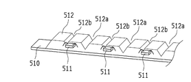
- a plurality of light-emitting elements 511... 511 are linearly arranged along the longitudinal direction on a long printed board 510, and this print
- a light emitting device that emits linear light by covering a plurality of light emitting elements 511... 511 on a substrate 510 with a sealing resin layer (transparent resin layer) 512 (see, for example, Patent Document 1).
- the recesses 512a and 512b are provided on the surface (surface opposite to the substrate) of the sealing resin layer 512 covering the light emitting elements 511. It can be taken out.
- a protective element for example, a Zener diode
- a substrate for example, Patent Document 2.
- the protective element for ensuring the electrostatic withstand voltage is connected in parallel to the light emitting element constituting the linear light source (see, for example, Patent Document 2).
- the product width width in the short direction of the long substrate
- the present invention has been made in consideration of such circumstances, and in a light emitting device including a protective element for protecting a light emitting element constituting a linear light source, a structure capable of suppressing the product width of the light emitting device to be small.
- the purpose is to provide.
- the present invention provides a light-emitting device that emits linear light using a plurality of light-emitting elements as light sources, and the plurality of light-emitting elements are linearly provided along the longitudinal direction of the long substrate. And a plurality of light emitting elements constituting the linear light source are connected in series, and protective elements are connected in parallel to the plurality of light emitting elements connected in series. It is connected. And the said protection element is arrange
- a plurality of light emitting elements constituting a linear light source are connected in series, a protection element is connected in parallel to the plurality of light emitting elements connected in series, and the protection element is arranged in the arrangement direction of the light emitting elements. Since it is disposed outside the end portion, the width of the substrate in the short direction, that is, the product width of the light emitting device can be reduced. Furthermore, since the protective element is arranged outside the end of the light emitting element in the arrangement direction, there is an effect that the possibility that the emitted light of the light emitting element is blocked by the protective element is reduced.
- the product width of the light emitting device can be more effectively reduced by disposing the protective element outside the end in the arrangement direction of the light emitting elements and on the extended line in the arrangement direction of the light emitting elements.
- a wiring pattern for connecting the protection elements in parallel to the plurality of light emitting elements for example, wiring that pulls back from the other end side of the substrate to one end side in order to connect the protection elements in parallel
- the product width of the light emitting device can be more effectively reduced.
- examples of the light emitting element include a light emitting diode
- examples of the protective element include a Zener diode.
- the linear light source composed of a plurality of light emitting elements arranged linearly on the substrate may be a single row (one line) of linear light sources, and the emission colors are different from each other. It may be a linear light source with two rows (two lines) or more.
- the light-emitting device including two or more rows of linear light sources include the following configurations.
- the first light-emitting element that emits the first color, the second light-emitting element that emits the second color, and the third light-emitting element that emits the third color are each in one direction (longitudinal direction of the substrate).
- a light-emitting device including a first linear light source, a second linear light source, and a third linear light source that are arranged in a straight line along the first linear light source and the second linear light source.
- the light emitting elements constituting the linear light sources of the light source and the third linear light source are connected in series, respectively, and a first protection element is connected in parallel to the plurality of first light emitting elements connected in series.
- a second protective element connected in parallel to the plurality of second light emitting elements connected in series, and a third protective element connected in parallel to the plurality of third light emitting elements connected in series.
- the first light emitting element is a blue light emitting element
- the second light emitting element is a red light emitting element
- the third light emitting element is a green light emitting element
- the first linear light source is a blue linear light source
- the second linear light source may be a red linear light source
- the third linear light source may be a green linear light source.
- a red linear light source composed of a red light emitting element at the center of the red light source, and a blue linear light source composed of a blue light emitting element and a green light emitting element on each side of the red linear light source.
- a configured green linear light source is arranged.
- the red light emitting element has a characteristic that the power consumption W (heat generation amount) is smaller than that of the blue / green light emitting element (blue / green LED chip).
- a light source (red LED chip) is placed in the center of the substrate where heat is likely to be trapped (the center in the direction in which the three linear light sources are arranged), and blue lines are formed on both sides of the red linear light source (on the outside of the substrate). By disposing the light source (blue LED chip) and the green linear light source (green LED chip), the heat radiation efficiency can be increased.
- the first linear light source (blue linear light source) is configured.
- a plurality of light emitting diodes, a plurality of light emitting diodes constituting a second linear light source (red linear light source), and a plurality of light emitting diodes constituting a third linear light source (green linear light source) Connect so that the anode is common.
- the degree of freedom of the wiring pattern formed on the substrate is increased, so that the width in the short direction of the substrate, that is, the product width of the light emitting device can be more effectively reduced. it can.
- the first linear light source blue linear light source
- the second linear light source red linear light source
- the third linear light source green
- Each linear light source can be individually driven and controlled.
- the three linear light sources are configured to be individually driven by the drive control device, for example, it is possible to obtain single color (for example, blue single color, red single color, green single color) and mixed light emission. It is possible to use the game machine in such a manner that the display color (light emission color) is changed according to the progress or content of the game. Further, for example, it is possible to use the display device or the lighting device by changing the display color or the lighting color according to time or season.
- a plurality of light emitting elements constituting a linear light source are connected in series, a protective element is connected in parallel to the plurality of light emitting elements connected in series, and the protective element is connected to the light emitting element. Since it arrange
- FIG. 1 is a perspective view schematically showing an example of the light-emitting device of the present invention.
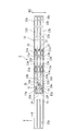
- FIG. 2 is a front view schematically showing an example of the light-emitting device of the present invention.
- the sealing resin layer is not shown.
- 3A is a surface view of a printed board used in the light emitting device shown in FIG.
- FIG. 3A shows a state where a light emitting diode chip and a Zener diode chip are mounted on a printed circuit board.
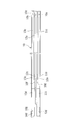
- 3B is a back view of the printed circuit board used in the light emitting device shown in FIG.
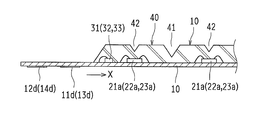
- FIG. 4 is a partial cross-sectional view of the light-emitting device shown in FIG. FIG.
- FIG. 5 is an equivalent circuit diagram showing a connection state of a plurality of light-emitting diode chips and Zener diode chips constituting each linear light source of the light-emitting device shown in FIGS. 1 to 3B.
- FIG. 6 is a diagram schematically showing a state in which a connector is connected to the light emitting device shown in FIGS. 1 to 3B.
- FIG. 7 is a schematic configuration diagram illustrating an example of a drive control device that drives and controls the light emitting device.
- FIG. 8 is a partial surface view showing a part of another example of the printed circuit board.
- FIG. 8 shows a state where a light emitting diode chip and a Zener diode chip are mounted on a printed circuit board.
- FIG. 9 is a perspective view schematically showing another example of the light emitting device of the present invention.
- FIG. 10 is a front view schematically showing another example of the light emitting device of the present invention. In FIG. 10, the sealing resin layer is not shown.
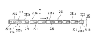
- FIG. 11A is a surface view of a printed circuit board used in the light emitting device shown in FIG.
- FIG. 11A shows a state where a light emitting diode chip and a Zener diode chip are mounted on a printed circuit board.
- FIG. 11B is a back view of the printed circuit board used in the light-emitting device shown in FIG. FIG.
- FIG. 12 is an equivalent circuit diagram showing a connection state of a plurality of light emitting diode chips and a Zener diode chip constituting the linear light source of the light emitting device shown in FIGS. 9 to 11B.
- FIG. 13 is a diagram schematically showing a modification of the light emitting device shown in FIGS. 9 to 11B.
- FIG. 14 is a partial perspective view showing an example of a conventional linear light-emitting device.
- the light-emitting device 1 of this example is a light-emitting device used for, for example, an amusement device such as a gaming machine (game machine), a display device such as a liquid crystal display panel, a lighting device, and the like.
- the printed circuit board 10 is a double-sided printed circuit board in which a wiring pattern and the like to be described later are formed on the front and back surfaces of a base material (for example, white glass BT (bismaleimide triazine)).
- a plurality of blue LED chips 21a... 21a are linearly arranged along the longitudinal direction (X direction) of the printed circuit board 10 on the printed circuit board 10.
- the blue LED chips 21a thus, a blue linear light source 21 is configured.
- a plurality of red LED chips 22a... 22a are linearly arranged on the printed circuit board 10 along the longitudinal direction (X direction) of the printed circuit board 10, and these red LED chips 22a.
- the red linear light source 22 is constituted by 22a.
- a plurality of green LED chips 23a... 23a are linearly arranged along the longitudinal direction (X direction) of the printed circuit board 10 on the printed circuit board 10, and these green LED chips 23a.
- a green linear light source 23 is configured.
- the blue line light source 21, red line light source 22, and green line light source 23 of these three lines (three rows) are arranged in parallel to each other, and the center of the three lines (three line light sources 21,
- a red linear light source 22 is disposed in the Y direction (the center of the direction orthogonal to the X direction) in which the lines 22 and 23 are arranged, and a blue linear light source is provided on both sides of the red linear light source 22 (on the outside of the printed circuit board 10).
- 21 and a green linear light source 23 are arranged.
- the blue linear light source 21, the red linear light source 22, and the green linear light source 23 of three lines are arranged adjacent to each other, and the distance between the blue linear light source 21 and the red linear light source 22.
- (Distance between LED chip centers) Da (see FIG. 2) and distance between red linear light source 22 and green linear light source 23 (distance between LED chip centers) Db (see FIG. 2) are equal. It has become. Further, in order to reduce the width W1 in the short side direction (Y direction) of the printed circuit board 10 (the product width W1 of the light emitting device 1), the distances Da and Db between the linear light sources are set as small as possible.
- the distance between the short side direction one end surface (edge) of the printed circuit board 10 and the blue LED chip 21a and the distance between the printed circuit board 10 and the other side surface (edge) in the short direction and the green LED chip 23a is as small as possible.
- each zener diode chip 31, 32, 33 is a protective element for securing electrostatic withstand voltage and protecting the LED chips 21a, 21a, 22a, 22a, 23a,. It is mounted on the substrate 10.
- the Zener diode chip 31 for blue line (hereinafter also referred to as the ZD chip 31 for blue line) is the arrangement direction (X direction) of the blue LED chips 21a. )
- the blue line ZD chip 31 is on a straight line L1 (FIG. 2) passing through the centers of the blue LED chips 21a, 21a arranged in the longitudinal direction (X direction) of the printed circuit board 10, It is mounted at a position on the outer side (outside in the LED chip arrangement direction) than the blue LED chip 21a at one end in the arrangement direction (the leftmost blue LED chip 21a in FIGS. 2 and 3A).
- the center of the blue line ZD chip 31 coincides with the straight line L1.
- the red line Zener diode chip 32 (hereinafter also referred to as the red line ZD chip 32) is disposed on an extension line in the arrangement direction (X direction) of the red LED chips 22a and 22a. More specifically, the red line ZD chip 32 is on a straight line L2 (see FIG. 2) passing through the centers of the red LED chips 22a, 22a arranged in the longitudinal direction (X direction) of the printed circuit board 10, The red LED chip 22a at one end in the chip arrangement direction is mounted on the outer side (outside in the LED chip arrangement direction) than the red LED chip 22a (the leftmost red LED chip 22a in FIGS. 2 and 3A). The center of the red line ZD chip 32 coincides with the straight line L2.
- the green line Zener diode chip 33 (hereinafter also referred to as the green line ZD chip 33) is disposed on an extended line in the arrangement direction (X direction) of the green LED chips 23a. More specifically, the green line ZD chip 33 is on a straight line L3 (see FIG. 2) passing through the centers of the green LED chips 23a,. The green LED chip 23a at one end in the chip array direction is mounted on the outer side (outside in the LED chip array direction) of the green LED chip 23a (the leftmost green LED chip 23a in FIGS. 2 and 3A). The center of the green line ZD chip 33 coincides with the straight line L3.
- the blue line ZD chips 31 and the red line ZD chips 32 are alternately arranged in the X direction, and the red line ZD chips 32 and the green line ZD chips 33 are alternately arranged in the X direction. Has been. The positions of the blue line ZD chip 31 and the green line ZD chip 33 in the X direction are the same.
- a sealing resin layer 40 made of a light transmissive resin is formed on the surface (chip mounting surface) side of the printed circuit board 10, and the printed circuit board is formed by the sealing resin layer 40.
- the LED chips 21a, 21a, 22a, 22a, 23a, 23a and the Zener diodes 31, 32, 33 on the 10 are covered.
- First concave portions 41... 41 and second concave portions 42... 42 are formed on the surface of the sealing resin layer 40 (the surface opposite to the printed board 10).
- Each first recess 41 is provided at a position corresponding to the center between adjacent LED chips 21a, 21a (22a, 22a, 23a, 23a), and each second recess 42 is formed in the LED chip 21a (22a). , 23a).
- the first recess 41 and the second recess 42 are grooves having a V-shaped cross section extending along the Y direction (a direction orthogonal to the X direction) in which the three lines of the linear light sources 21, 22, and 23 are arranged.
- the LED chips 21a, 21a, 22a, 22a, 23a are provided in the sealing resin layer 40.
- the outgoing light of 23a can be efficiently extracted outside (see, for example, Japanese Patent Application Laid-Open No. 2009-021221).
- the phosphor is not contained in the sealing resin layer 40 of this embodiment.
- FIG. 4 is a partial cross-sectional view of the light emitting device 1.
- the LED chips 21a, 21a (22a, 22a, 23a, 23a) mounted on the printed circuit board 10 and the Zener diodes 31 (32, 33) are sealed. Covered with a resin layer 40.
- a first recess 41 and a second recess 42 are formed on the surface of the sealing resin layer 40 (the surface opposite to the printed circuit board 10).
- the 1st recessed part 41 is provided in the position corresponding to the center between LED chip 21a, 21a (22a, 22a, 23a, 23a) adjacent to each other.
- the 2nd recessed part 42 is provided in the position corresponding to LED chip 21a (22a, 23a).
- connection wiring patterns 11a,... 11a and an anode wiring pattern 11b for blue lines and a plurality of connection wiring patterns 12a,.
- a wiring pattern 12b, a plurality of connection wiring patterns 13a,... 13a and an anode wiring pattern 13b for the green line, and a cathode common wiring pattern 14 are formed.
- the connection between the LED chip or the ZD chip and various patterns is “electrical connection”.
- connection wiring patterns 12a, .. 12a and anode wiring patterns 12b for the red line are arranged in the center in the short direction (Y direction) of the printed circuit board 10, and on both sides thereof, respectively.
- a plurality of connection wiring patterns 11a,... 11a and anode wiring patterns 11b for blue lines, and a plurality of connection wiring patterns 13a,... 13a and anode wiring patterns 13b for green lines are arranged.
- the anode wiring patterns 11b, 12b, and 13b for each line are disposed on the other end side (the right end side in FIG. 3A) in the longitudinal direction (X direction) of the printed circuit board 10.
- the cathode common wiring pattern 14 is disposed on one end side in the longitudinal direction of the printed circuit board 10 (left end side in FIG. 3A).
- connection wiring patterns 11a, 12a, and 13a for each line and the anode wiring patterns 11b, 12b, and 13b are substantially strip-shaped wiring patterns that extend along the X direction.
- the cathode common wiring pattern 14 is provided with a blue line connection portion 14a, a red line connection portion 14b, and a green line connection portion 14c, each extending in a substantially strip shape along the X direction.
- connection wiring patterns 11a,... 11a for the blue line are arranged at predetermined intervals along the X direction, and the connection wiring pattern 11a at the other end in the wiring pattern arrangement direction (most in FIG. 3A).
- the connection wiring pattern 11a) at the right end is located in the vicinity of the anode wiring pattern 11b for the blue line.
- the connection wiring pattern 11 a at one end in the wiring pattern arrangement direction (the leftmost connection wiring pattern 11 a in FIG. 3A) is positioned in the vicinity of the blue line connection portion 14 a of the cathode common wiring pattern 14.
- the blue line anode wiring pattern 11b, the blue line connection wiring patterns 11a... 11a, and the blue line connection part 14a are arranged on the same line along the X direction.
- connection wiring patterns 12a... 12a for the red line are arranged at predetermined intervals along the X direction, and the connection wiring pattern 12a at the other end in the wiring pattern arrangement direction (most in FIG. 3A).
- the rightmost connection wiring pattern 12a) is located in the vicinity of the anode wiring pattern 12b for the red line.
- connection wiring pattern 12 a at one end in the wiring pattern arrangement direction is located in the vicinity of the red line connection portion 14 b of the cathode common wiring pattern 14.
- the red line anode wiring pattern 12b, the red line connection wiring patterns 12a, 12a, and the red line connection portion 14b are arranged on the same line along the X direction.
- connection wiring patterns 13a, 13a for the green line are arranged at predetermined intervals along the X direction, and the connection wiring pattern 13a at the other end in the wiring pattern arrangement direction (the rightmost end in FIG. 3A).
- the connection wiring pattern 13a) is located in the vicinity of the anode wiring pattern 13b for the green line.
- connection wiring pattern 13 a at one end in the wiring pattern arrangement direction is located in the vicinity of the green line connection portion 14 c of the cathode common wiring pattern 14.
- the green line anode wiring pattern 13b, the green line connection wiring patterns 13a, 13a, and the green line connection portion 14c are arranged on the same line along the X direction.
- a blue LED chip (front surface two-electrode type) 21a is mounted on an end portion (end portion on the other end side) of the blue line connection portion 14a of the cathode common wiring pattern 14, and the blue LED chip is formed by wire bonding.
- the cathode 21a is connected to the blue line connecting portion 14a, and the anode is connected to the blue line connecting wiring pattern 11a adjacent to the blue line connecting portion 14a.
- blue LED chips 21a are mounted on the connection wiring patterns 11a.
- the cathode is connected to the connection wiring pattern 11a on which the blue LED chip 21a is mounted by wire bonding, and the anode is connected to the adjacent connection wiring pattern 11a by wire bonding. Yes.
- the anode of the blue LED chip 21a mounted on the connection wiring pattern 11a at the other end in the wiring pattern arrangement direction is connected to the anode wiring pattern 11b for the blue line.
- a plurality of blue LED chips 21a... 21a constituting the blue linear light source 21 are connected in series.
- a red LED chip (front surface two-electrode type) 22a is mounted on the end portion (end portion on the other end side) of the red line connection portion 14b of the cathode common wiring pattern 14, and the red LED chip is formed by wire bonding.
- the cathode of 22a is connected to the red line connection portion 14b, and the anode is connected to the connection wiring pattern 12a for red line adjacent to the red line connection portion 14b.
- red LED chips 22a are mounted on the connection wiring patterns 12a,.
- the cathode is connected to the connection wiring pattern 12a on which the red LED chip 22a is mounted by wire bonding, and the anode is connected to the adjacent connection wiring pattern 12a by wire bonding. Yes.
- the anode of the red LED chip 22a mounted on the connection wiring pattern 12a at the other end in the wiring pattern arrangement direction is connected to the anode wiring pattern 12b for the red line.
- a green LED chip (front surface two-electrode type) 23a is mounted on the end portion (end portion on the other end side) of the green line connection portion 14c of the cathode common wiring pattern 14, and the green LED chip is formed by wire bonding.
- the cathode of 23a is connected to the green line connection part 14c, and the anode is connected to the connection wiring pattern 13a for the green line adjacent to the green line connection part 14c.
- green LED chips 23a are mounted on the connection wiring patterns 13a, 13a, respectively.
- the cathode is connected to the connection wiring pattern 13a on which the green LED chip 23a is mounted by wire bonding, and the anode is connected to the adjacent connection wiring pattern 13a by wire bonding. Yes.
- the anode of the green LED chip 23a mounted on the connection wiring pattern 13a at the other end in the wiring pattern arrangement direction is connected to the anode wiring pattern 13b for the green line.
- the blue line ZD chip 31, the red line ZD chip 32, and the green line ZD chip 33 are mounted on the cathode common wiring pattern 14 of the printed circuit board 10. As described above, these three ZD chips 31, 32, and 33 are arranged outside the LED chips 21a, 22a, and 23a of the respective colors located at one end in the LED chip arrangement direction (outside in the LED chip arrangement direction). ing. In addition, an opening from which a part of the cathode common wiring pattern 14 is removed is provided in the vicinity of the three ZD chips 31, 32, 33, and the opening serves as a wire bond area 16 for ZD. Yes.
- a wire bond pad 15a for a blue line, a wire bond pad 15b for a red line, and a wire bond pad 15c for a green line are formed.
- the wire bond pad 15a for the blue line and the wire bond pad 15b for the red line are alternately arranged in the X direction, and the wire bond pad 15b for the red line and the wire bond pad 15c for the green line are They are arranged alternately in the X direction.
- the width of the printed board 10 in the short direction (Y direction) that is, the product width W1 of the light emitting device 1 can be reduced.
- the positions of the wire bond pad 15a for the blue line and the wire bond pad 15c for the green line in the X direction are the same.
- the blue line wire bond pads 15a and the red line wire bond pads 15b, which are alternately arranged, may be arranged so as to partially overlap in the X direction.
- the red line wire bond pads 15b and the green line wire bond pads 15c that are alternately arranged may be partially overlapped in the X direction.
- the dimension (product length) in the longitudinal direction of the printed circuit board 10 can be reduced.
- the wire bond pad 15a for the blue line and the wire bond pad 15c for the green line may be arranged so that the positions in the X direction are shifted from each other.
- the blue line ZD chip 31, the red line ZD chip 32, and the green line ZD chip 33 are upper and lower electrode type chips.
- the blue line ZD chip 31 is mounted on the cathode common wiring pattern 14 by die bonding, and the anode of the blue line ZD chip 31 is connected to the cathode common wiring pattern 14.
- the cathode of the blue line ZD chip 31 is connected to the wire bond pad 15a (anode wiring pattern 11c) for the blue line by wire bonding.
- the red line ZD chip 32 is mounted on the cathode common wiring pattern 14 by die bonding, and the anode of the red line ZD chip 32 is connected to the cathode common wiring pattern 14.
- the cathode of the red line ZD chip 32 is connected to the wire bond pad 15b (anode wiring pattern 12c) for the red line by wire bonding.
- the green line ZD chip 33 is mounted on the cathode common wiring pattern 14 by die bonding, and the anode of the green line ZD chip 33 is connected to the cathode common wiring pattern 14.
- the cathode of the green line ZD chip 33 is connected to the green line wire bond pad 15c (anode wiring pattern 13c) by wire bonding.
- an anode wiring pattern 11c for blue lines, an anode wiring pattern 12c for red lines, and an anode wiring pattern for green lines. 13c is formed on the back surface of the printed circuit board 10 (the surface opposite to the LED / ZD chip mounting surface).
- the anode wiring patterns 11c, 12c, and 13c on the back surface of the substrate are wiring patterns for pulling back the anode line to one end side (left end side in FIG. 3B) of the printed circuit board 10, and from the other end portion of the printed circuit board 10 to one end side. It extends along the X direction.
- the blue line anode wiring pattern 11c on the back surface of the printed circuit board 10 is connected to the blue line anode wiring pattern 11b on the surface of the printed circuit board 10 through the through-hole wiring 10a.
- the blue line anode wiring pattern 11c is connected to the blue line wire bond pad 15a on the surface of the printed circuit board 10 through a through-hole wiring 10d.
- the anode wiring pattern 12c for red line on the back surface of the printed board 10 is connected to the anode wiring pattern 12b for red line on the surface of the printed board 10 through the through-hole wiring 10b.
- the anode wiring pattern 12c for red line is connected to the wire bonding pad 15b for red line on the surface of the printed board 10 through the through-hole wiring 10e.
- the anode wiring pattern 13c for the green line on the back surface of the printed board 10 is connected to the anode wiring pattern 13b for the green line on the surface of the printed board 10 through the through-hole wiring 10c.
- the green line anode wiring pattern 13c is connected to the green line wire bond pad 15c on the surface of the printed board 10 through a through-hole wiring 10f.
- anode terminals 11d, 12d, and 13d are formed at one end portions of the anode wiring patterns 11c, 12c, and 13c on the back surface of the printed circuit board 10, respectively.
- the red line anode terminal 12d is disposed at one end (the left end in FIG. 3B) of the printed circuit board 10, and the blue line anode terminal 11d and the green anode
- the terminal 13d is disposed at a position spaced apart from the red line anode terminal 12d.
- a cathode terminal 14d is formed at one end of the back surface of the printed circuit board 10.
- the cathode terminal 14d on the back surface of the printed circuit board 10 is connected to the cathode common wiring pattern 14 on the surface of the printed circuit board 10 through a through-hole wiring 10g.
- a plurality of blue LED chips 21 a... 21 a constituting the blue linear light source 21 and a plurality of red LED chips 22 a. 22a and a plurality of green LED chips 23a,... 23a constituting the green linear light source 23 are connected in series, and these series-connected blue LED chips 21a,... 21a and red LED chips 22a,. And the green LED chips 23a... 23a are connected by cathode common connection.
- the blue line ZD chip 31 is connected in parallel with a reverse polarity to the plurality of blue LED chips 21a, 21a connected in series, and to the plurality of red LED chips 22a, 22a connected in series.
- the red line ZD chips 32 are connected in parallel with reverse polarity.
- the green line ZD chip 33 is connected in parallel with the reverse polarity to the plurality of green LED chips 23a.
- the light emitting device 1 of this embodiment four terminals (three anode terminals 11d, 12d, 13d, and cathode terminal 14d) are taken out from one end of the printed circuit board 10, and a lead wire-connector connection structure is adopted. By doing so, the light emitting device 1 can be connected to the drive control device 100 described later by a connector. Specifically, as shown in FIG. 6, three anode terminals 11 d, 12 d, 13 d arranged on one end side (left end side in FIG. 6) of the printed circuit board 10 are connected to the connector 5 with lead wires 51, 52, 53. The cathode terminal 14d is connected to the connector 5 via a lead wire 54.
- a ZD chip as a protection element connected in parallel to each LED chip group constituting the linear light sources 21, 22, 23 of each color 31, 32, and 33 are arranged outside the LED chips 21 a, 22 a, and 23 a of the respective colors located at the ends in the LED chip arrangement direction (outside in the LED chip arrangement direction).
- a wiring (anode wiring patterns 11c, 12c, 13c) for pulling back the anode lines of the linear light sources 21, 22, and 23 of the respective colors from the other end of the printed circuit board 10 to one end side is formed on the back surface of the printed circuit board 10. The wiring pattern on the surface of the printed circuit board 10 is reduced.
- the wire bond pads 15a, 15b and 15c for each line are arranged alternately.
- the cathode terminal 14d is made common by adopting cathode common connection.
- the ZD chips 31, 32, and 33 are arranged outside the end portions in the arrangement direction of the LED chips 21a, 22a, and 23a, the emitted light from the LED chips 21a, 22a, and 23a is emitted. The possibility of being blocked by the ZD chips 31, 32, 33 is reduced.
- the red LED chip 22a is a red LED chip 22a, 22a in consideration of the point that the power consumption W (heat generation amount) is smaller than that of the blue / green LED chips 21a, 23a.
- the configured red linear light source 22 is arranged at the center of the printed circuit board 10 where heat is easily trapped (the center in the Y direction in which three lines of linear light sources 21, 22, and 23 are arranged).
- a blue linear light source 21 composed of blue LED chips 21a... 21a and a green linear light source 23 composed of green LED chips 23a... 23a are arranged on both sides (outside of the printed circuit board 10). Therefore, the heat dissipation efficiency can be increased.
- the drive control apparatus 100 in this example includes a control unit 101, three drive circuits 121, 122, 123, a DC power supply unit 103, and the like.
- the drive circuit 121 is connected to the anode side of the blue LED chips 21 a, 21 a constituting the blue linear light source 21.
- the drive circuit 122 is connected to the anode side of the red LED chips 22a, 22a constituting the red linear light source 22.
- the drive circuit 123 is connected to the anode side of the green LED chips 23a... 23a constituting the green linear light source 23.
- a DC power supply unit 103 that supplies power to each of the blue linear light source 21, the red linear light source 22, and the green linear light source 23 is connected to the drive circuits 121, 122, and 123.
- the DC power supply unit 103 rectifies an alternating current supplied from a commercial alternating current power source and converts it into a predetermined voltage and supplies the direct current to the drive circuits 121, 122, 123 and the control unit 101.
- the DC power supply unit 103 may be configured to be able to use a battery (DC) in combination, or the DC power supply unit may be configured by only the battery (DC).
- the control unit 101 responds to a light emission control signal (a signal for instructing light emission control to be described later) from an external device (for example, a gaming machine, a display device, a lighting device or the like), and a red linear light source.
- a light emission control signal (a signal for instructing light emission control to be described later) from an external device (for example, a gaming machine, a display device, a lighting device or the like), and a red linear light source.
- (Duty signal for each) is output to the drive circuits 121, 122, 123.
- the drive circuits 121, 122, and 123 send drive currents to the blue linear light source 21 (blue LED chip 21 a...
- the blue linear light source 21, the red linear light source 22, and the green linear light source 23 that constitute the light emitting device 1 can be individually driven and controlled. Can be emitted. Specific examples of light emission control that emits light of each color are listed below.
- Control for supplying a drive current only to the blue linear light source 21 to emit blue monochromatic light (a1) Supplying drive current only to the blue linear light source 21 intermittently (repeat ON / OFF) to turn blue Control for performing monochromatic blinking light emission (b) Control for supplying driving current only to the red linear light source 22 to emit red single color light (b1) Supplying driving current only to the red linear light source 22 (ON / OFF) (C) Control for supplying driving current only to the green linear light source 23 to emit green single color (c1) Control for driving only the green linear light source 23 Control that emits green single color flashing light by intermittent supply (repeat ON / OFF) (d) Monochromatic light emission for a certain period of time, such as [Blue single color light emission] ⁇ [Red single color light emission] ⁇ [Green single color light emission] Control to switch every time Order is arbitrary) (E) Control for supplying white current by supplying a drive current to all of the blue linear light source 21, the red linear light source 22 and
- the light emitting device 1 of this embodiment it is possible to obtain light emission of blue, red, green, white, and mixed colors.
- a usage method such as changing the display color (light emission color) in accordance with this becomes possible.
- the display device or the lighting device it is possible to use the display device or the lighting device in such a manner that the display color or the lighting color is changed according to time or season.
- the light-emitting device 1 of this embodiment can be suitably used for amusement equipment such as game machines, display devices, lighting devices, and the like.
- the ZD chips 31, 32, 33 are arranged on the extended line in the LED chip arrangement direction (X direction) (arranged on the center lines L1, L2, L3). Without limitation, it is a position outside the LED chips 21a, 22a, and 23a located at one end in the LED chip arrangement direction (outside in the LED chip arrangement direction), and the product width W1 of the light emitting device 1 (of the printed circuit board 10). As long as the width W1) can be reduced, the ZD chips 31, 32, and 33 may be arranged at positions shifted from the extended line in the LED chip arrangement direction (X direction).
- the ZD chips 31, 32, and 33 are mounted on the line connecting portions 14a, 14b, and 14c of the respective colors of the cathode common wiring pattern 14, but instead, the wire bond pad 15a. , 15b, 15c may be equipped with ZD chips 31, 32, 33, respectively.
- anode terminals 11d, 12d, 13d and cathode terminal 14d are taken out from one end side of the printed circuit board 10, but the present invention is not limited thereto, and the anode terminal 11d is not limited thereto.
- 12d, and 13d may be arranged on the other end side (the right end side in FIG. 3B) of the printed circuit board 10 (see FIG. 13).
- the blue LED chips 21a, 21a connected in series, the red LED chips 22a, 22a connected in series, and the green LED chips 23a, 23a connected in series are connected by cathode common connection.
- the blue LED chips 21a, 21a connected in series, the red LED chips 22a, 22a connected in series, and the green LED chips 23a, 23a connected in series are anodes. You may make it connect by common connection.
- an opening from which a part of the cathode common wiring pattern 14 is removed is provided in the vicinity of the ZD chips 31, 32, 33, and the opening is used as the wire bond area 16 for ZD.
- the cathode common wiring pattern 14 (two patterns) is provided on both sides of the wire bond pad 15a for line and the wire bond pad 15c for green line (see FIG. 3A), but is not limited thereto.
- a cathode common wiring pattern 14 '(one pattern) may be provided between a wire bond pad 15a for a blue line and a wire bond pad 15c for a green line. If the structure shown in FIG.
- the width in the short direction of the printed circuit board 10 ′ that is, the product width W1 of the light emitting device 1 can be further reduced.
- the product width W1 of the light emitting device 1 can be reduced to about 1.31 mm.
- a blue LED chip, a red LED chip, and a green LED chip are used.
- three lines of light emission colors different from each other are used.
- a light source may be configured.
- the number of lines of the linear light source is not limited to three lines, and the present invention can be applied to a light emitting device having two lines or four lines or more.
- the light emitting diode chip (LED chip) is used as the light emitting element.
- the present invention is not limited to this, and the light emitting device may be configured using another light emitting element.
- a blue EL (electroluminescence) element for example, using a blue EL (electroluminescence) element, a red EL element, and a green EL element, a blue linear light source (21), a red linear light source (22), a green line as shown in FIGS.
- a shaped light source (23) may be configured.
- the light-emitting device 200 of this example is a light-emitting device used for an amusement device such as a gaming machine (game machine), a display device such as a liquid crystal display panel, a lighting device, and the like.
- Light emitting diode chips hereinafter also referred to as LED chips
- LED chips Light emitting diode chips
- Each LED chip 221 emits blue light, for example.
- the printed circuit board 201 is a double-sided printed circuit board in which a wiring pattern and the like to be described later are formed on the front and back surfaces of a base material (for example, white glass BT (bismaleimide triazine)).
- a plurality of LED chips 221... 221 are linearly arranged along the longitudinal direction (X direction) of the printed circuit board 201 on the printed circuit board 201, and the LED chips 221.
- a light source 202 is formed.
- the width W2 in the short direction of the printed board 201 the product width W2 of the light emitting device 200
- the distance between the LED chip 211, the printed circuit board 201, and the other end face (edge) in the short direction is set to be as small as possible.
- Zener diode chips 203 (hereinafter also referred to as ZD chips 203) are provided for the plurality of LED chips 221 and 221 constituting the linear light source 202.
- the ZD chip 203 is a protective element for securing the electrostatic withstand voltage and protecting the LED chips 221... 221 from electrostatic breakdown, and is mounted on the printed circuit board 201.
- the ZD chip 203 is arranged on an extension line in the arrangement direction (X direction) of the LED chips 221. More specifically, the ZD chip 203 is on a straight line L4 (FIG. 10) passing through the centers of the LED chips 221... 221 aligned in the longitudinal direction (X direction) of the printed circuit board 201, and is one end in the LED chip arrangement direction. LED chip 221 (the leftmost LED chip 221 in FIGS. 10 and 11A) is mounted outside (in the LED chip array direction). The center of the ZD chip 203 coincides with the straight line L4.
- a sealing resin layer 204 is formed on the surface (chip mounting surface) side of the printed board 201, and the LED chips 221. -The 221 and the ZD chip 203 are covered.
- a sealing resin layer 204 is formed after applying a resin containing a phosphor around the LED chip 221.
- the dispersed phosphor is, for example, a phosphor that emits yellow light. By combining such a phosphor and the LED chip 221 that emits blue light, white light can be emitted.
- First recesses 241... 241 and second recesses 242... 242 are formed on the surface of the sealing resin layer 204 (surface opposite to the printed circuit board 201). Each first recess 241 is provided at a position corresponding to the center between the LED chips 221 and 221 adjacent to each other, and each second recess 242 is provided at a position corresponding to the LED chip 221.
- the first recess 241 and the second recess 242 are grooves having a V-shaped cross section extending along the Y direction orthogonal to the arrangement direction of the LED chips 221.
- connection wiring patterns 211a, 211a, an anode wiring pattern 211b, and a cathode wiring pattern 212a are formed on the surface (chip mounting surface) of the printed circuit board 201.
- the anode wiring pattern 211b is disposed on the other end side in the longitudinal direction of the printed board 201 (the right end side in FIG. 11A). Further, the cathode wiring pattern 212a is arranged on one end side (left end side in FIG. 11A) in the longitudinal direction (X direction) of the printed circuit board 201, and a plurality of the cathode wiring patterns 212a are arranged between the anode wiring pattern 211b and the cathode wiring pattern 212a. Strip-like connection wiring patterns 211a, 211a are arranged.
- connection wiring patterns 211a, 211a are arranged at predetermined intervals along the X direction, and the connection wiring pattern 211a at the other end in the wiring pattern arrangement direction (the rightmost connection wiring pattern 211a in FIG. 11A). ) Is located in the vicinity of the anode wiring pattern 211b. Further, the connection wiring pattern 211a at the one end in the wiring pattern arrangement direction (the leftmost connection wiring pattern 211a in FIG. 11A) is located in the vicinity of the cathode wiring pattern 212a.
- the anode wiring pattern 211b, the connection wiring patterns 211a, 211a and the cathode wiring pattern 212a are arranged on the same line along the X direction.
- an LED chip (front surface two-electrode type) 221 is mounted on an end portion (end portion on the other end side) of the cathode wiring pattern 212a, and the cathode of the LED chip 211 becomes a cathode wiring pattern 212a by wire bonding.
- the anode is connected to the connection wiring pattern 211a adjacent to the cathode wiring pattern 212a.
- the LED chip 211 is mounted on each of the connection wiring patterns 211a and 211a.
- the cathode is connected to the connection wiring pattern 211a on which the LED chip 211 is mounted by wire bonding, and the anode is connected to the adjacent connection wiring pattern 211a by wire bonding.
- the anode of the LED chip 221 mounted on the connection wiring pattern 211a at the other end in the wiring pattern arrangement direction is connected to the anode wiring pattern 211b.
- the plurality of LED chips 221... 221 constituting the linear light source 202 are connected in series.
- the ZD chip 203 is mounted on the cathode wiring pattern 212a of the printed board 201. As described above, the ZD chip 203 is disposed outside the LED chip 221 located at one end in the LED chip arrangement direction (outside in the LED chip arrangement direction). Further, a notch portion in which a part of the cathode wiring pattern 212 a is notched is provided in the vicinity of the ZD chip 203, and this notch portion serves as a wire bond area 214 for ZD. A wire bond pad 213 is formed in the wire bond area 214.
- the ZD chip 203 is a top and bottom electrode type chip.
- the ZD chip 203 is mounted on the cathode wiring pattern 212a by die bonding, and the anode of the ZD chip 203 is connected to the cathode wiring pattern 212a.
- the cathode of the ZD chip 203 is connected to a wire bond pad 213 (anode terminal 211d) by wire bonding.
- an anode wiring pattern 211c is formed on the back surface (surface opposite to the chip mounting surface) of the printed circuit board 201.
- the anode wiring pattern 211c on the back surface of the printed circuit board 201 is a wiring pattern for pulling back the anode line to one end side (the left end side in FIG. 11B) of the printed circuit board 201. It extends along the X direction.
- the anode wiring pattern 211c on the back surface of the printed circuit board 201 is connected to the anode wiring pattern 211b on the surface of the printed circuit board 201 through a through-hole wiring 201a. Further, the anode wiring pattern 211c (anode terminal 211d) on the back surface of the printed circuit board 201 is connected to the wire bond pad 213 on the surface of the printed circuit board 201 through the through-hole wiring 201b. An anode terminal 211d is formed at one end of the anode wiring pattern 211c on the back surface of the printed board 201 (one end of the printed board 201).
- the reason why the anode terminal 211d is provided at one end of the printed circuit board 201 is to allow the two terminals of the anode terminal 211d and the cathode terminal 212b described below to be taken out from one end side of the printed circuit board 201.
- a cathode terminal 212b is formed at one end of the back surface of the printed circuit board 201.
- the cathode terminal 212b on the back surface of the printed circuit board 201 is connected to the cathode wiring pattern 212a on the surface of the printed circuit board 201 through the through-hole wiring 201c.
- the plurality of LED chips 221, 221 constituting the linear light source 202 are connected in series, and the plurality of LED chips 221 connected in series are further connected.
- ..ZD chip 203 is connected to 221 in parallel with reverse polarity.
- the linear light source 202 is driven (driven to the LED chips 221... 221 by a drive control device including a drive circuit (one circuit) and a control unit as shown in FIG. (Current supply) may be controlled.
- a drive control device including a drive circuit (one circuit) and a control unit as shown in FIG. (Current supply) may be controlled.
- the ZD chip 203 as a protection element is connected in parallel to the LED chips 221... 221 connected in series, and the ZD chip 203 is connected to the end in the LED chip arrangement direction.
- the LED chip 221 of each color located in the section is arranged outside (in the LED chip arrangement direction).
- a wiring (anode wiring pattern 211c) for pulling back the anode line of the linear light source 202 from the other end of the printed circuit board 201 to one end side is formed on the back surface of the printed circuit board 201 to reduce the wiring pattern on the surface of the printed circuit board 201.
- the width W2 of the printed circuit board 201 in the short direction that is, the product width W2 of the light emitting device 200 can be reduced by devising the layout of the chip, wiring, and electrodes. For example, assuming that a 300 ⁇ m ⁇ 300 ⁇ m LED chip or ZD chip is used, the product width W2 of the light emitting device 200 can be reduced to about 0.4 mm.
- the ZD chip 203 is arranged outside the end of the LED chip 221 in the arrangement direction, the possibility that the emitted light of the LED chip 221 is blocked by the ZD chip 221 is reduced.
- two terminals are taken out from one end side of the printed board 201.
- An anode terminal 211 d ′ may be disposed at the other end so that the terminal is taken out from both ends of the printed board 201.
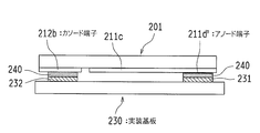
- the cathode terminal 212b and the anode terminal 211d ′ disposed at both ends of the printed board 201 are joined to the land patterns 232 and 231 of the mounting board 230 using the solders 240 and 240, respectively. The whole may be mounted on the mounting substrate 230.
- the light emitting diode chip (LED chip) is used as the light emitting element.
- the present invention is not limited to this, and the light emitting device may be configured using other light emitting elements.
- a linear light source (202) as shown in FIGS. 9 to 11B may be configured using an EL (electroluminescence) element.
- the present invention is not limited to this, and for example, monochromatic light emission of each color of blue, red, and green, or The present invention can also be applied to a light emitting device that performs mixed color light emission other than white.
- the present invention can be used for a light-emitting device that emits linear light using a plurality of light-emitting elements as a light source, and more specifically, can be effectively used for a light-emitting device that includes a protective element for protecting the light-emitting element. it can.
Landscapes
- Engineering & Computer Science (AREA)
- General Engineering & Computer Science (AREA)
- Led Device Packages (AREA)
- Arrangement Of Elements, Cooling, Sealing, Or The Like Of Lighting Devices (AREA)
- Planar Illumination Modules (AREA)
- Circuit Arrangement For Electric Light Sources In General (AREA)
- Microelectronics & Electronic Packaging (AREA)
Abstract
Description
本発明の発光装置の一例について図1~図5を参照して説明する。
次に、この実施形態の発光装置1の回路構成について図3A及び図3Bを参照して説明する。
以上説明したように、この実施形態の発光装置1によれば、(1)各色の線状光源21,22,23を構成する各LEDチップ群に対して並列に接続した保護素子としてのZDチップ31,32,33を、それぞれ、LEDチップ配列方向の端部に位置する各色のLEDチップ21a,22a,23aの外側(LEDチップ配列方向の外側)に配置している。(2)各色の線状光源21,22,23のアノードラインをプリント基板10の他端部から一端側に引き戻す配線(アノード配線パターン11c,12c,13c)をプリント基板10の裏面に形成して、プリント基板10表面の配線パターンを少なくしている。(3)各ライン用のワイヤボンドパッド15a,15b,15cを互い違いに配置している。(4)カソードコモン接続を採用してカソード端子14dを共通化している。このようなチップ・配線・電極のレイアウトの工夫により、プリント基板10の短手方向の幅W1つまり発光装置1の製品幅W1を小さくすることができる。例えば、300μm×300μmのLEDチップ、ZDチップを使用すると仮定した場合、発光装置1の製品幅W1を1.4mm程度にまで小さくすることができる。
次に、発光装置1の発光を制御する駆動制御装置について図7を参照して説明する。
上述の如く、この実施形態では、発光装置1を構成する青色線状光源21、赤色線状光源22及び緑色線状光源23をそれぞれ個別に駆動制御することができるので、複数色の線状光を発光することが可能になる。その各色の発光を行う発光制御の具体的な例について以下に列記する。
(a1)青色線状光源21のみに駆動電流を断続的に供給(ON/OFFの繰り返し)して青色単色の点滅発光を行う制御
(b)赤色線状光源22のみに駆動電流を供給して赤色単色の発光を行う制御
(b1)赤色線状光源22のみに駆動電流を断続的に供給(ON/OFFの繰り返し)して赤色単色の点滅発光を行う制御
(c)緑色線状光源23のみに駆動電流を供給して緑色単色の発光を行う制御
(c1)緑色線状光源23のみに駆動電流を断続的に供給(ON/OFFの繰り返し)して緑色単色の点滅発光を行う制御
(d)[青色単色発光]→[赤色単色発光]→[緑色単色発光]のように、単色発光を一定時間ごとに切り替える制御(なお、各色の発光順は任意)
(e)青色線状光源21、赤色線状光源22及び緑色線状光源23の全てに駆動電流を供給して白色の発光を行う制御
(f)青色線状光源21及び赤色線状光源22に駆動電流を供給して青色と赤色との混色を発光する制御(この場合、青色線状光源21と赤色線状光源22との発光強度の比率を適宜に調整することにより任意の色の混色(合成色)を得ることができる。)
(g)青色線状光源21及び緑色線状光源23に駆動電流を供給して青色と緑色との混色を発光する制御(この場合、青色線状光源21と緑色線状光源23との発光強度の比率を適宜に調整することにより任意の色の混色(合成色)を得ることができる。)
(h)赤色線状光源22及び緑色線状光源23に駆動電流を供給して赤色と緑色との混色を発光する制御(この場合、赤色線状光源22と緑色線状光源23との発光強度の比率を適宜に調整することにより任意の色の混色(合成色)を得ることができる。)
(i)青色線状光源21、赤色線状光源22及び緑色線状光源23の全てに駆動電流を供給するとともに、その青色線状光源21と赤色線状光源22と緑色線状光源23との発光強度の比率を適宜に調整することにより、青色と赤色と緑色とを混色した任意の色(合成色)の線状光を発光する制御
なお、発光制御は上記した例に限られることなく、他の任意の形態の発光を行う制御であってもよい。
まず、図14に示す従来の線状の発光装置では発光素子から放出された光を、蛍光体が分散された封止樹脂層に照射することにより白色光を発光する構造であるため、発光色が単色(白色)に限定されるという課題がある。
以上の[実施形態1]では、ZDチップ31,32,33を、LEDチップ配列方向(X方向)の延長線上に配置(中心線L1,L2,L3上に配置)しているが、これに限られることなく、LEDチップ配列方向の一端部に位置するLEDチップ21a,22a,23aの外側(LEDチップ配列方向の外側)の位置であって、発光装置1の製品幅W1(プリント基板10の幅W1)を小さくすることが可能な位置であれば、LEDチップ配列方向(X方向)の延長線上からずれた位置にZDチップ31,32,33を配置してもよい。
本発明の発光装置の他の例について図9~図12を参照して説明する。
次に、この例の発光装置200の回路構成について図11A及び図11Bを参照して説明する。
以上説明したように、この実施形態によれば、直列接続したLEDチップ221・・221に対して保護素子としてのZDチップ203を並列に接続するとともに、ZDチップ203を、LEDチップ配列方向の端部に位置する各色のLEDチップ221の外側(LEDチップ配列方向の外側)に配置している。さらに、線状光源202のアノードラインをプリント基板201の他端部から一端側に引き戻す配線(アノード配線パターン211c)をプリント基板201の裏面に形成してプリント基板201表面の配線パターンを少なくしているので、このようなチップ・配線・電極のレイアウトの工夫により、プリント基板201の短手方向の幅W2つまり発光装置200の製品幅W2を小さくすることができる。例えば、300μm×300μmのLEDチップ、ZDチップを使用すると仮定した場合、発光装置200の製品幅W2を0.4mm程度にまで小さくすることができる。
以上の[実施形態2]では、プリント基板201の一端側から2端子(アノード端子211d及びカソード端子212b)を取り出す構造としているが、これに替えて、図13に示すように、プリント基板201の他端部にアノード端子211d′を配置して、プリント基板201の両端から端子を取り出すようにしてもよい。この場合、プリント基板201の両端に配置したカソード端子212bとアノード端子211d′とを、それぞれ、はんだ240,240を用いて実装基板230のランドパターン232,231に接合することにより、発光装置200の全体を実装基板230に搭載するようにしてもよい。
10 プリント基板
10a・・10g スルーホール配線
11a 接続配線パターン(青色)
11b アノード配線パターン(表面)
11c アノード配線パターン(裏面)
11d アノード端子
12a 接続配線パターン(赤色)
12b アノード配線パターン(表面)
12c アノード配線パターン(裏面)
12d アノード端子
13a 接続配線パターン(緑色)
13b アノード配線パターン(表面)
13c アノード配線パターン(裏面)
13d アノード端子
14 カソードコモン配線パターン
14a 青色ライン接続部
14b 赤色ライン接続部
14c 緑色ライン接続部
14d カソード端子
15a,15b,15c ワイヤボンドパッド
16 ワイヤボンドエリア
21 青色線状光源
21a 青色発光ダイオードチップ(青色LEDチップ)
22 赤色線状光源
22a 赤色発光ダイオードチップ(赤色LEDチップ)
23 緑色線状光源
23a 赤色発光ダイオードチップ(赤色LEDチップ)
31,32,33 ツェナーダイオードチップ(ZDチップ)
200 発光装置
201 プリント基板
201a,201b,201c スルーホール配線
211a 接続配線パターン
211b アノード配線パターン(表面)
211c アノード配線パターン(裏面)
211d,211d′ アノード端子
212a カソード配線パターン
212b カソード端子
203 ツェナーダイオードチップ(ZDチップ)
213 ワイヤボンドパッド
214 ワイヤボンドエリア
Claims (12)
- 複数の発光素子を光源として線状光を発光する発光装置であって、
長尺状の基板上に複数の発光素子が当該基板の長手方向に沿って直線状に配列されてなる線状光源を備え、前記線状光源を構成する複数の発光素子が直列に接続されているとともに、前記直列に接続された複数の発光素子に対して保護素子が並列に接続されており、
前記保護素子は、前記基板上であって、前記複数の発光素子のうち配列方向の端部に位置する発光素子の当該配列方向の外側に配置されていることを特徴とする発光装置。 - 請求項1記載の発光装置において、
前記保護素子は、前記複数の発光素子の配列方向の延長線上に配置されていることを特徴とする発光装置。 - 請求項1または2記載の発光装置において、
前記複数の発光素子に対して保護素子を並列に接続するための配線パターンが、前記基板の前記発光素子の搭載面とは反対側となる裏面に形成されていることを特徴とする発光装置。 - 請求項1~3のいずれか1つに記載の発光装置において、
前記発光素子が発光ダイオードであり、前記保護素子がツェナーダイオードであることを特徴とする発光装置。 - 請求項1~4のいずれか1つに記載の発光装置において、
複数の発光素子が前記基板の長手方向に沿って直線状に配列されてなる、1列の線状光源を備えていることを特徴とする発光装置。 - 請求項1~4のいずれか1つに記載の発光装置において、
発光色が互いに異なる発光素子が、それぞれ、前記基板の長手方向に沿って直線状に複数配列されてなる、少なくとも2列の線状光源を備えていることを特徴とする発光装置。 - 請求項6記載の発光装置において、
第1の色を発光する第1発光素子と第2の色を発光する第2発光素子と第3の色を発光する第3発光素子とが、それぞれ、一方向に沿って直線状に複数配列されてなる第1線状光源と第2線状光源と第3線状光源とを有し、
前記第1線状光源、前記第2線状光源及び前記第3線状光源の各線状光源を構成する発光素子がそれぞれ直列に接続されているとともに、前記直列に接続された複数の第1発光素子に対して第1保護素子が並列に接続され、前記直列に接続された複数の第2発光素子に対して第2保護素子が並列に接続され、前記直列に接続された複数の第3発光素子に対して第3保護素子が並列に接続されていることを特徴とする発光装置。 - 請求項7記載の発光装置において、
前記第1発光素子が青色発光素子、前記第2発光素子が赤色発光素子、前記第3発光素子が緑色発光素子であり、前記第1線状光源が青色線状光源、前記第2線状光源が赤色線状光源、前記第3線状光源が緑色線状光源であることを特徴とする発光装置。 - 請求項8記載の発光装置において、
前記3つの線状光源が並ぶ方向の中央に、前記赤色発光素子で構成される赤色線状光源が配置され、その赤色線状光源の両側に、それぞれ、前記青色発光素子で構成される青色線状光源と、前記緑色発光素子で構成される緑色線状光源とが配置されていることを特徴とする発光装置。 - 請求項7~9のいずれか1つに記載の発光装置において、
前記各線状光源を構成する発光素子は発光ダイオードであって、前記第1線状光源を構成する複数の発光ダイオードと、前記第2線状光源を構成する複数の発光ダイオードと、前記第3線状光源を構成する複数の発光ダイオードとは、カソードコモンとなるように接続されていることを特徴とする発光装置。 - 請求項7~9のいずれか1つに記載の発光装置において、
前記各線状光源を構成する発光素子は発光ダイオードであって、前記第1線状光源を構成する複数の発光ダイオードと、前記第2線状光源を構成する複数の発光ダイオードと、前記第3線状光源を構成する複数の発光ダイオードとは、アノードコモンとなるように接続されていることを特徴とする発光装置。 - 請求項7~11のいずれか1つに記載の発光装置において、
前記第1線状光源、前記第2線状光源及び第3線状光源は、駆動制御装置によってそれぞれ個別に駆動されることを特徴とする発光装置。
Priority Applications (2)
| Application Number | Priority Date | Filing Date | Title |
|---|---|---|---|
| US14/413,299 US20150173137A1 (en) | 2012-07-13 | 2013-06-24 | Light-emitting device |
| CN201380036505.7A CN104428582B (zh) | 2012-07-13 | 2013-06-24 | 发光装置 |
Applications Claiming Priority (2)
| Application Number | Priority Date | Filing Date | Title |
|---|---|---|---|
| JP2012-157979 | 2012-07-13 | ||
| JP2012157979A JP5522643B2 (ja) | 2012-07-13 | 2012-07-13 | 発光装置 |
Publications (1)
| Publication Number | Publication Date |
|---|---|
| WO2014010394A1 true WO2014010394A1 (ja) | 2014-01-16 |
Family
ID=49915860
Family Applications (1)
| Application Number | Title | Priority Date | Filing Date |
|---|---|---|---|
| PCT/JP2013/067214 Ceased WO2014010394A1 (ja) | 2012-07-13 | 2013-06-24 | 発光装置 |
Country Status (5)
| Country | Link |
|---|---|
| US (1) | US20150173137A1 (ja) |
| JP (1) | JP5522643B2 (ja) |
| CN (1) | CN104428582B (ja) |
| TW (1) | TWI539575B (ja) |
| WO (1) | WO2014010394A1 (ja) |
Families Citing this family (7)
| Publication number | Priority date | Publication date | Assignee | Title |
|---|---|---|---|---|
| JP6480714B2 (ja) * | 2014-11-19 | 2019-03-13 | サムテック・イノベーションズ株式会社 | 物品検査装置 |
| JP2017093897A (ja) * | 2015-11-26 | 2017-06-01 | 株式会社藤商事 | 遊技機 |
| JP6408516B2 (ja) | 2016-07-01 | 2018-10-17 | ミネベアミツミ株式会社 | 面状照明装置及び基板 |
| JP2020174012A (ja) * | 2019-04-12 | 2020-10-22 | 株式会社ジャパンディスプレイ | 光源装置、及び光源装置を有する表示装置 |
| CN110536508B (zh) * | 2019-07-31 | 2024-09-13 | 格瑞电子(厦门)有限公司 | 一种三基色led灯组阵列排列电路板 |
| CN112268237B (zh) * | 2020-10-20 | 2022-06-21 | 深圳市好兵光电科技有限公司 | 一种多基色无光斑柔性灯带 |
| CN220172128U (zh) * | 2023-07-04 | 2023-12-12 | 深圳市洲明科技股份有限公司 | 一种节能显示模组 |
Citations (7)
| Publication number | Priority date | Publication date | Assignee | Title |
|---|---|---|---|---|
| JP2002090735A (ja) * | 2000-09-13 | 2002-03-27 | Canon Inc | 電子機器 |
| JP2006324355A (ja) * | 2005-05-17 | 2006-11-30 | Sharp Corp | フレキシブル配線基板、電子部品搭載フレキシブル配線基板、および液晶表示装置 |
| JP2008270701A (ja) * | 2007-03-22 | 2008-11-06 | Toshiba Lighting & Technology Corp | 発光装置および照明器具 |
| JP2009071227A (ja) * | 2007-09-18 | 2009-04-02 | Panasonic Corp | Ledモジュール |
| JP2010152304A (ja) * | 2008-11-20 | 2010-07-08 | Fuji Electric Fa Components & Systems Co Ltd | 照光表示装置 |
| JP2011014355A (ja) * | 2009-07-01 | 2011-01-20 | Casio Computer Co Ltd | 発光装置、液晶表示装置及び静電破壊防止構造 |
| JP2012227290A (ja) * | 2011-04-18 | 2012-11-15 | Panasonic Corp | 発光装置、バックライトユニット、液晶表示装置及び照明装置 |
Family Cites Families (13)
| Publication number | Priority date | Publication date | Assignee | Title |
|---|---|---|---|---|
| JP3686569B2 (ja) * | 2000-03-02 | 2005-08-24 | シャープ株式会社 | 半導体発光装置及びそれを用いた表示装置 |
| TWI235349B (en) * | 2001-11-26 | 2005-07-01 | Osram Opto Semiconductors Gmbh | Circuit-arrangement for an LED-array |
| WO2004073065A1 (ja) * | 2003-02-14 | 2004-08-26 | Hitachi, Ltd. | 半導体素子駆動用集積回路及び電力変換装置 |
| KR100751455B1 (ko) * | 2005-09-16 | 2007-08-23 | 삼성전자주식회사 | 액정표시장치 |
| JP4172501B2 (ja) * | 2006-05-31 | 2008-10-29 | ソニー株式会社 | 発光ダイオード点灯回路、照明装置及び液晶表示装置 |
| JP4300223B2 (ja) * | 2006-06-30 | 2009-07-22 | 株式会社 日立ディスプレイズ | 照明装置および照明装置を用いた表示装置 |
| JP5045166B2 (ja) * | 2007-03-16 | 2012-10-10 | ソニー株式会社 | 光源装置及び液晶表示装置 |
| CN101354867B (zh) * | 2007-07-26 | 2010-06-23 | 苏州璨宇光学有限公司 | 背光模组及其驱动装置 |
| JP5388676B2 (ja) * | 2008-12-24 | 2014-01-15 | イビデン株式会社 | 電子部品内蔵配線板 |
| JP5619381B2 (ja) * | 2009-07-09 | 2014-11-05 | ピーエスフォー ルクスコ エスエイアールエルPS4 Luxco S.a.r.l. | 半導体装置及び半導体装置の製造方法 |
| JP4910023B2 (ja) * | 2009-08-27 | 2012-04-04 | シャープ株式会社 | 光源装置 |
| JP2011165833A (ja) * | 2010-02-08 | 2011-08-25 | Toshiba Corp | Ledモジュール |
| KR20120067026A (ko) * | 2010-12-15 | 2012-06-25 | 삼성전자주식회사 | 백라이트 유닛 |
-
2012
- 2012-07-13 JP JP2012157979A patent/JP5522643B2/ja not_active Expired - Fee Related
-
2013
- 2013-06-24 CN CN201380036505.7A patent/CN104428582B/zh not_active Expired - Fee Related
- 2013-06-24 WO PCT/JP2013/067214 patent/WO2014010394A1/ja not_active Ceased
- 2013-06-24 US US14/413,299 patent/US20150173137A1/en not_active Abandoned
- 2013-07-11 TW TW102124943A patent/TWI539575B/zh not_active IP Right Cessation
Patent Citations (7)
| Publication number | Priority date | Publication date | Assignee | Title |
|---|---|---|---|---|
| JP2002090735A (ja) * | 2000-09-13 | 2002-03-27 | Canon Inc | 電子機器 |
| JP2006324355A (ja) * | 2005-05-17 | 2006-11-30 | Sharp Corp | フレキシブル配線基板、電子部品搭載フレキシブル配線基板、および液晶表示装置 |
| JP2008270701A (ja) * | 2007-03-22 | 2008-11-06 | Toshiba Lighting & Technology Corp | 発光装置および照明器具 |
| JP2009071227A (ja) * | 2007-09-18 | 2009-04-02 | Panasonic Corp | Ledモジュール |
| JP2010152304A (ja) * | 2008-11-20 | 2010-07-08 | Fuji Electric Fa Components & Systems Co Ltd | 照光表示装置 |
| JP2011014355A (ja) * | 2009-07-01 | 2011-01-20 | Casio Computer Co Ltd | 発光装置、液晶表示装置及び静電破壊防止構造 |
| JP2012227290A (ja) * | 2011-04-18 | 2012-11-15 | Panasonic Corp | 発光装置、バックライトユニット、液晶表示装置及び照明装置 |
Also Published As
| Publication number | Publication date |
|---|---|
| JP5522643B2 (ja) | 2014-06-18 |
| TW201409662A (zh) | 2014-03-01 |
| CN104428582A (zh) | 2015-03-18 |
| TWI539575B (zh) | 2016-06-21 |
| US20150173137A1 (en) | 2015-06-18 |
| JP2014022117A (ja) | 2014-02-03 |
| CN104428582B (zh) | 2016-04-27 |
Similar Documents
| Publication | Publication Date | Title |
|---|---|---|
| JP5522643B2 (ja) | 発光装置 | |
| JP3968226B2 (ja) | 発光ユニット用ジョイント基板 | |
| US8622578B2 (en) | Flexible LED array | |
| US10234112B2 (en) | Light source module and lighting device having same | |
| JP2013118292A (ja) | Led発光装置 | |
| JP5216948B1 (ja) | 基板、発光装置及び照明装置 | |
| US20110309381A1 (en) | Light-emitting device and lighting apparatus | |
| JP6649969B2 (ja) | 照明デバイス、照明デバイスを備えた照明装置、および照明デバイスの動作方法 | |
| JP5408414B2 (ja) | 発光モジュール | |
| JP6486099B2 (ja) | Led発光モジュール | |
| KR101071020B1 (ko) | 조명용 led 모듈 및 이를 포함하는 조명장치 | |
| US20220196230A1 (en) | Light-emitting module and planar light source having the same | |
| JP6264640B2 (ja) | 照明装置 | |
| US8888324B2 (en) | Light-emitting device, method for assembling same and luminaire | |
| KR101104755B1 (ko) | 발광 장치 | |
| WO2013015037A1 (ja) | 発光装置 | |
| KR101602861B1 (ko) | 발광 소자 | |
| KR101469058B1 (ko) | 발광소자 패키지 및 그 제조 방법 | |
| TWI438370B (zh) | 光源模組 | |
| CN220648164U (zh) | Led灯及led产品 | |
| TWM458670U (zh) | 光電整合之發光二極體陣列封裝結構 | |
| KR101104763B1 (ko) | 발광 장치 | |
| KR101104767B1 (ko) | 발광 장치 | |
| KR101119016B1 (ko) | 발광 장치 | |
| KR101333478B1 (ko) | Led 패키지 모듈 |
Legal Events
| Date | Code | Title | Description |
|---|---|---|---|
| WWE | Wipo information: entry into national phase |
Ref document number: 201380036505.7 Country of ref document: CN |
|
| 121 | Ep: the epo has been informed by wipo that ep was designated in this application |
Ref document number: 13816106 Country of ref document: EP Kind code of ref document: A1 |
|
| WWE | Wipo information: entry into national phase |
Ref document number: 14413299 Country of ref document: US |
|
| NENP | Non-entry into the national phase |
Ref country code: DE |
|
| 122 | Ep: pct application non-entry in european phase |
Ref document number: 13816106 Country of ref document: EP Kind code of ref document: A1 |