WO2014007024A1 - 表示装置および表示方法 - Google Patents
表示装置および表示方法 Download PDFInfo
- Publication number
- WO2014007024A1 WO2014007024A1 PCT/JP2013/065791 JP2013065791W WO2014007024A1 WO 2014007024 A1 WO2014007024 A1 WO 2014007024A1 JP 2013065791 W JP2013065791 W JP 2013065791W WO 2014007024 A1 WO2014007024 A1 WO 2014007024A1
- Authority
- WO
- WIPO (PCT)
- Prior art keywords
- pixel
- display
- subpixel
- signal
- frame
- Prior art date
- Legal status (The legal status is an assumption and is not a legal conclusion. Google has not performed a legal analysis and makes no representation as to the accuracy of the status listed.)
- Ceased
Links
Images















Classifications
-
- G—PHYSICS
- G09—EDUCATION; CRYPTOGRAPHY; DISPLAY; ADVERTISING; SEALS
- G09G—ARRANGEMENTS OR CIRCUITS FOR CONTROL OF INDICATING DEVICES USING STATIC MEANS TO PRESENT VARIABLE INFORMATION
- G09G3/00—Control arrangements or circuits, of interest only in connection with visual indicators other than cathode-ray tubes
- G09G3/20—Control arrangements or circuits, of interest only in connection with visual indicators other than cathode-ray tubes for presentation of an assembly of a number of characters, e.g. a page, by composing the assembly by combination of individual elements arranged in a matrix no fixed position being assigned to or needed to be assigned to the individual characters or partial characters
- G09G3/2007—Display of intermediate tones
- G09G3/2077—Display of intermediate tones by a combination of two or more gradation control methods
- G09G3/2081—Display of intermediate tones by a combination of two or more gradation control methods with combination of amplitude modulation and time modulation
-
- G—PHYSICS
- G09—EDUCATION; CRYPTOGRAPHY; DISPLAY; ADVERTISING; SEALS
- G09G—ARRANGEMENTS OR CIRCUITS FOR CONTROL OF INDICATING DEVICES USING STATIC MEANS TO PRESENT VARIABLE INFORMATION
- G09G3/00—Control arrangements or circuits, of interest only in connection with visual indicators other than cathode-ray tubes
- G09G3/20—Control arrangements or circuits, of interest only in connection with visual indicators other than cathode-ray tubes for presentation of an assembly of a number of characters, e.g. a page, by composing the assembly by combination of individual elements arranged in a matrix no fixed position being assigned to or needed to be assigned to the individual characters or partial characters
- G09G3/2007—Display of intermediate tones
- G09G3/2018—Display of intermediate tones by time modulation using two or more time intervals
- G09G3/2022—Display of intermediate tones by time modulation using two or more time intervals using sub-frames
- G09G3/2025—Display of intermediate tones by time modulation using two or more time intervals using sub-frames the sub-frames having all the same time duration
-
- G—PHYSICS
- G09—EDUCATION; CRYPTOGRAPHY; DISPLAY; ADVERTISING; SEALS
- G09G—ARRANGEMENTS OR CIRCUITS FOR CONTROL OF INDICATING DEVICES USING STATIC MEANS TO PRESENT VARIABLE INFORMATION
- G09G3/00—Control arrangements or circuits, of interest only in connection with visual indicators other than cathode-ray tubes
- G09G3/20—Control arrangements or circuits, of interest only in connection with visual indicators other than cathode-ray tubes for presentation of an assembly of a number of characters, e.g. a page, by composing the assembly by combination of individual elements arranged in a matrix no fixed position being assigned to or needed to be assigned to the individual characters or partial characters
- G09G3/2007—Display of intermediate tones
- G09G3/2074—Display of intermediate tones using sub-pixels
-
- G—PHYSICS
- G09—EDUCATION; CRYPTOGRAPHY; DISPLAY; ADVERTISING; SEALS
- G09G—ARRANGEMENTS OR CIRCUITS FOR CONTROL OF INDICATING DEVICES USING STATIC MEANS TO PRESENT VARIABLE INFORMATION
- G09G3/00—Control arrangements or circuits, of interest only in connection with visual indicators other than cathode-ray tubes
- G09G3/20—Control arrangements or circuits, of interest only in connection with visual indicators other than cathode-ray tubes for presentation of an assembly of a number of characters, e.g. a page, by composing the assembly by combination of individual elements arranged in a matrix no fixed position being assigned to or needed to be assigned to the individual characters or partial characters
- G09G3/2007—Display of intermediate tones
- G09G3/2077—Display of intermediate tones by a combination of two or more gradation control methods
-
- G—PHYSICS
- G09—EDUCATION; CRYPTOGRAPHY; DISPLAY; ADVERTISING; SEALS
- G09G—ARRANGEMENTS OR CIRCUITS FOR CONTROL OF INDICATING DEVICES USING STATIC MEANS TO PRESENT VARIABLE INFORMATION
- G09G3/00—Control arrangements or circuits, of interest only in connection with visual indicators other than cathode-ray tubes
- G09G3/20—Control arrangements or circuits, of interest only in connection with visual indicators other than cathode-ray tubes for presentation of an assembly of a number of characters, e.g. a page, by composing the assembly by combination of individual elements arranged in a matrix no fixed position being assigned to or needed to be assigned to the individual characters or partial characters
- G09G3/34—Control arrangements or circuits, of interest only in connection with visual indicators other than cathode-ray tubes for presentation of an assembly of a number of characters, e.g. a page, by composing the assembly by combination of individual elements arranged in a matrix no fixed position being assigned to or needed to be assigned to the individual characters or partial characters by control of light from an independent source
- G09G3/36—Control arrangements or circuits, of interest only in connection with visual indicators other than cathode-ray tubes for presentation of an assembly of a number of characters, e.g. a page, by composing the assembly by combination of individual elements arranged in a matrix no fixed position being assigned to or needed to be assigned to the individual characters or partial characters by control of light from an independent source using liquid crystals
- G09G3/3611—Control of matrices with row and column drivers
- G09G3/3614—Control of polarity reversal in general
-
- G—PHYSICS
- G09—EDUCATION; CRYPTOGRAPHY; DISPLAY; ADVERTISING; SEALS
- G09G—ARRANGEMENTS OR CIRCUITS FOR CONTROL OF INDICATING DEVICES USING STATIC MEANS TO PRESENT VARIABLE INFORMATION
- G09G3/00—Control arrangements or circuits, of interest only in connection with visual indicators other than cathode-ray tubes
- G09G3/20—Control arrangements or circuits, of interest only in connection with visual indicators other than cathode-ray tubes for presentation of an assembly of a number of characters, e.g. a page, by composing the assembly by combination of individual elements arranged in a matrix no fixed position being assigned to or needed to be assigned to the individual characters or partial characters
- G09G3/34—Control arrangements or circuits, of interest only in connection with visual indicators other than cathode-ray tubes for presentation of an assembly of a number of characters, e.g. a page, by composing the assembly by combination of individual elements arranged in a matrix no fixed position being assigned to or needed to be assigned to the individual characters or partial characters by control of light from an independent source
- G09G3/36—Control arrangements or circuits, of interest only in connection with visual indicators other than cathode-ray tubes for presentation of an assembly of a number of characters, e.g. a page, by composing the assembly by combination of individual elements arranged in a matrix no fixed position being assigned to or needed to be assigned to the individual characters or partial characters by control of light from an independent source using liquid crystals
- G09G3/3611—Control of matrices with row and column drivers
- G09G3/3648—Control of matrices with row and column drivers using an active matrix
-
- G—PHYSICS
- G09—EDUCATION; CRYPTOGRAPHY; DISPLAY; ADVERTISING; SEALS
- G09G—ARRANGEMENTS OR CIRCUITS FOR CONTROL OF INDICATING DEVICES USING STATIC MEANS TO PRESENT VARIABLE INFORMATION
- G09G3/00—Control arrangements or circuits, of interest only in connection with visual indicators other than cathode-ray tubes
- G09G3/20—Control arrangements or circuits, of interest only in connection with visual indicators other than cathode-ray tubes for presentation of an assembly of a number of characters, e.g. a page, by composing the assembly by combination of individual elements arranged in a matrix no fixed position being assigned to or needed to be assigned to the individual characters or partial characters
- G09G3/34—Control arrangements or circuits, of interest only in connection with visual indicators other than cathode-ray tubes for presentation of an assembly of a number of characters, e.g. a page, by composing the assembly by combination of individual elements arranged in a matrix no fixed position being assigned to or needed to be assigned to the individual characters or partial characters by control of light from an independent source
- G09G3/36—Control arrangements or circuits, of interest only in connection with visual indicators other than cathode-ray tubes for presentation of an assembly of a number of characters, e.g. a page, by composing the assembly by combination of individual elements arranged in a matrix no fixed position being assigned to or needed to be assigned to the individual characters or partial characters by control of light from an independent source using liquid crystals
- G09G3/3611—Control of matrices with row and column drivers
- G09G3/3648—Control of matrices with row and column drivers using an active matrix
- G09G3/3655—Details of drivers for counter electrodes, e.g. common electrodes for pixel capacitors or supplementary storage capacitors
-
- G—PHYSICS
- G09—EDUCATION; CRYPTOGRAPHY; DISPLAY; ADVERTISING; SEALS
- G09G—ARRANGEMENTS OR CIRCUITS FOR CONTROL OF INDICATING DEVICES USING STATIC MEANS TO PRESENT VARIABLE INFORMATION
- G09G2300/00—Aspects of the constitution of display devices
- G09G2300/04—Structural and physical details of display devices
- G09G2300/0439—Pixel structures
- G09G2300/0452—Details of colour pixel setup, e.g. pixel composed of a red, a blue and two green components
-
- G—PHYSICS
- G09—EDUCATION; CRYPTOGRAPHY; DISPLAY; ADVERTISING; SEALS
- G09G—ARRANGEMENTS OR CIRCUITS FOR CONTROL OF INDICATING DEVICES USING STATIC MEANS TO PRESENT VARIABLE INFORMATION
- G09G2300/00—Aspects of the constitution of display devices
- G09G2300/04—Structural and physical details of display devices
- G09G2300/0439—Pixel structures
- G09G2300/0465—Improved aperture ratio, e.g. by size reduction of the pixel circuit, e.g. for improving the pixel density or the maximum displayable luminance or brightness
-
- G—PHYSICS
- G09—EDUCATION; CRYPTOGRAPHY; DISPLAY; ADVERTISING; SEALS
- G09G—ARRANGEMENTS OR CIRCUITS FOR CONTROL OF INDICATING DEVICES USING STATIC MEANS TO PRESENT VARIABLE INFORMATION
- G09G2300/00—Aspects of the constitution of display devices
- G09G2300/08—Active matrix structure, i.e. with use of active elements, inclusive of non-linear two terminal elements, in the pixels together with light emitting or modulating elements
- G09G2300/0876—Supplementary capacities in pixels having special driving circuits and electrodes instead of being connected to common electrode or ground; Use of additional capacitively coupled compensation electrodes
-
- G—PHYSICS
- G09—EDUCATION; CRYPTOGRAPHY; DISPLAY; ADVERTISING; SEALS
- G09G—ARRANGEMENTS OR CIRCUITS FOR CONTROL OF INDICATING DEVICES USING STATIC MEANS TO PRESENT VARIABLE INFORMATION
- G09G2320/00—Control of display operating conditions
- G09G2320/02—Improving the quality of display appearance
- G09G2320/0271—Adjustment of the gradation levels within the range of the gradation scale, e.g. by redistribution or clipping
- G09G2320/0276—Adjustment of the gradation levels within the range of the gradation scale, e.g. by redistribution or clipping for the purpose of adaptation to the characteristics of a display device, i.e. gamma correction
-
- G—PHYSICS
- G09—EDUCATION; CRYPTOGRAPHY; DISPLAY; ADVERTISING; SEALS
- G09G—ARRANGEMENTS OR CIRCUITS FOR CONTROL OF INDICATING DEVICES USING STATIC MEANS TO PRESENT VARIABLE INFORMATION
- G09G2320/00—Control of display operating conditions
- G09G2320/02—Improving the quality of display appearance
- G09G2320/028—Improving the quality of display appearance by changing the viewing angle properties, e.g. widening the viewing angle, adapting the viewing angle to the view direction
Definitions
- the present invention relates to a display device that displays input image data having a resolution different from the resolution of the display panel.
- a conventional display device displays an input image enlarged or reduced when the resolution of the input image data is different from the resolution of the display panel (for example, Patent Document 1). That is, when the number of pixels of the input image is different from the total number of pixels of the display panel, display is performed with a number of pixels different from the number of pixels of the input image on the display panel.
- the bilinear method and the bicubic method are known as methods for enlarging / reducing the input image.
- pixels that do not exist in the input image are interpolated by averaging or weighted average from the values of surrounding pixels, or the pixels of the input image are thinned out by using operations such as filter processing.
- An output value corresponding to the pixel is obtained and displayed.
- the information such as the outline and color included in the original input image data cannot be completely reproduced.
- the number of pixels decreases depending on the resolution on the output side (the total number of pixels of the display panel), so that color blurring occurs and the image quality is deteriorated.
- a low-pass filter (LPF) process is performed on an input signal, and then a sampling process is performed according to the resolution on the output side (display panel side).
- the cutoff characteristic of the LPF is designed with 1 ⁇ 2 of the maximum frequency that can be displayed on the output side as a guide. Due to the characteristics of this LPF, blurring and distortion occur in the reduced image. These blurs and distortions are fundamental and cannot be avoided by conventional methods.
- the present invention has been made in view of the above problems, and an object of the present invention is to provide a display device and a display capable of displaying an input image having a resolution higher than that of the display panel without degrading display quality. It is to provide a method.
- a display device provides A display device that displays an image by dividing one frame into m (m; an integer of 2 or more) subframes, Each pixel of the display unit has a first sub-pixel and a second sub-pixel having different brightness from each other, In each pixel, the first sub-pixel and the second sub-pixel each display a high-brightness and low-brightness image by switching for each subframe,
- the input signal input from the outside to the display device has a vertical resolution different from that of the display panel, An image corresponding to the input signal is displayed by changing a voltage supplied to each pixel for each subframe.
- the display device performs so-called frame division driving and pixel division driving. Further, in the display device, in each pixel, the light and dark display states of the first subpixel and the second subpixel are switched for each subframe, and the voltage supplied to each pixel is different for each subframe. . As a result, the luminance of each of the first subpixel and the second subpixel can be controlled independently. Therefore, for example, when one pixel is composed of two subpixels and one frame is divided into two subframes for display, an input signal having a vertical resolution twice that of the display panel can be displayed. it can.
- an input image having a resolution higher than that of the display panel can be displayed without degrading the display quality.
- a control unit that outputs display signals of the first to m-th subframes to the display unit,
- the first subpixel and the second subpixel are connected to the same data signal line and the same scanning signal line, and are connected to different storage capacitor lines
- the control unit causes the storage capacitor wiring signal supplied to the storage capacitor wiring corresponding to the first subpixel and the storage capacitor wiring signal supplied to the storage capacitor wiring corresponding to the second subpixel in different directions.
- level shifting changing the direction of level shifting within one frame for each, inverting the voltage polarity of the display signal at the frame period, and making the voltage of the display signal different for each subframe, It is preferable to provide a luminance difference between the first subpixel and the second subpixel.
- the bright subpixel and the dark subpixel can be formed in each pixel by shifting the voltage level of the storage capacitor wiring signal supplied to the storage capacitor wiring.
- One frame is divided into two subframes, The first subpixel and the second subpixel are arranged side by side in the row direction and alternately arranged in the column direction,
- the input signal preferably has a vertical resolution twice that of the display panel.
- a high-resolution image (horizontal 1920 ⁇ vertical 2160) can be displayed on an FHD (horizontal 1920 ⁇ vertical 1080) liquid crystal panel.
- the direction of the level shift of the storage capacitor line signal given to one storage capacitor line is different between subframes in one frame, and is different between the last subframe of one frame and the first subframe of the subsequent frame. Preferably they are equal to each other.
- the display device From the gray level at which the luminance of the display signal is minimized to the gray level at which the luminance is 0.5, only the first sub-pixel is turned on, It is preferable to turn on the first subpixel and the second subpixel above the gray level at which the luminance of the display signal is 0.5.
- the display unit displays from 0 gradation to 255 gradation
- the gradation when the luminance is 0.5 is 186 gradations.
- the storage capacitor wiring signal given to one storage capacitor wiring does not shift in level during the writing of the signal voltage to the pixel electrode forming the storage capacitor wiring and the capacitor, and is synchronized with the end of the writing or Thereafter, it is preferable to shift the level in the plus direction or the minus direction with respect to the reference voltage.
- the direction of the level shift of the storage capacitor wiring signal is reversed between one of the two pixel electrodes included in one pixel and the storage capacitor wiring forming the capacitor and the other storage capacitor wiring forming the capacitor. Is preferred.
- a configuration in which one pixel electrode included in one of two pixels adjacent in the scanning direction and one pixel electrode included in the other form the same storage capacitor wiring and capacitance may be employed.
- a display device includes: Each of the above pixels is composed of four types of color pixels that display different colors. Each of the four types of color pixels may include the first subpixel and the second subpixel.
- a display device includes: The four types of color pixels are a red pixel that displays red, a green pixel that displays green, a blue pixel that displays blue, and a yellow pixel that displays yellow. These color pixels are repeatedly arranged in this order in the row direction. It can also be set as the structure.
- a display method for displaying an image by dividing one frame into m (m; an integer of 2 or more) subframes,
- Each pixel of the display unit has a first sub-pixel and a second sub-pixel having different brightness from each other,
- the first sub-pixel and the second sub-pixel each display a high-brightness and low-brightness image by switching for each subframe
- the input signal input from the outside to the display device has a vertical resolution different from that of the display panel
- An image corresponding to the input signal is displayed by changing a voltage supplied to each pixel for each subframe.
- the display method includes: An output step of outputting display signals of the first to m-th subframes to the display unit;
- the first subpixel and the second subpixel are connected to the same data signal line and the same scanning signal line, and are connected to different storage capacitor lines,
- the storage capacitor wiring signal supplied to the storage capacitor wiring corresponding to the first subpixel and the storage capacitor wiring signal supplied to the storage capacitor wiring corresponding to the second subpixel are in different directions.
- level shifting changing the direction of level shifting within one frame for each, inverting the voltage polarity of the display signal at the frame period, and making the voltage of the display signal different for each subframe, It is preferable to provide a luminance difference between the first subpixel and the second subpixel.
- the display method according to the present invention includes: Divide one frame into two subframes, The first subpixel and the second subpixel are arranged side by side in the row direction and alternately arranged in the column direction,
- the input signal preferably has a vertical resolution twice that of the display panel.
- each display method the same effect as each display device can be obtained.
- the first subpixel and the second subpixel each display a high-luminance image and a low-luminance image for each subframe.
- an image corresponding to the input signal is displayed. Accordingly, since the brightness of each of the first subpixel and the second subpixel can be controlled independently, the display device reduces the display quality of an input image having a resolution higher than that of the display panel. It can be displayed without.
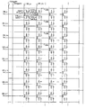
- FIG. 3 is a plan view schematically showing a pixel arrangement of the liquid crystal display device according to Embodiment 1.
- FIG. 3 is an equivalent circuit diagram of a partial region of the liquid crystal display device according to Embodiment 1.
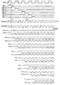
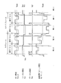
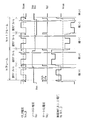
- the liquid crystal display device according to Embodiment 1 it is a diagram showing the cycle and phase of the CS voltage supplied to the CS line with reference to the voltage waveform of the gate line, and the voltage of each subpixel electrode.
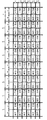
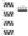
- 4 is a schematic diagram illustrating a driving state of the liquid crystal display device according to Embodiment 1.
- FIG. 1 is a schematic diagram illustrating a driving state of the liquid crystal display device according to Embodiment 1.
- FIG. 4 is a schematic diagram illustrating a driving state of the liquid crystal display device according to Embodiment 1.
- FIG. (A) is a schematic diagram which shows the normal drive method of the conventional liquid crystal display device
- (b) is a schematic diagram which shows the drive method of the liquid crystal display device which concerns on Embodiment 1.
- FIG. 4 is a schematic diagram illustrating a display state of sub-frames of sub-pixels in the liquid crystal display device according to Embodiment 1.
- FIG. 6 is a schematic diagram illustrating a display signal control method in the liquid crystal display device according to Embodiment 1.
- FIG. 6 is a schematic diagram showing a schematic configuration of a liquid crystal display device according to Embodiment 2.
- FIG. 6 is an equivalent circuit diagram illustrating one pixel of a liquid crystal panel in a liquid crystal display device according to Embodiment 2.
- FIG. FIG. 6 is an equivalent circuit diagram illustrating one pixel of a liquid crystal panel in a liquid crystal display device according to Embodiment 2.
- 6 is a plan view showing a connection relationship of part of a liquid crystal panel in a liquid crystal display device according to a second embodiment.
- 6 is a plan view schematically showing a display state of a part of a liquid crystal panel in a liquid crystal display device according to Embodiment 2.
- FIG. It is a graph which shows the display brightness
- 6 is a graph showing a result of subframe display in which a front display signal and a rear display signal are divided into front and rear subframes and output in the liquid crystal display device according to the second embodiment.
- (A) is a figure which shows the relationship between the voltage polarity (polarity of the voltage between electrodes) and a frame period in the 1st method of inverting the polarity of the voltage between electrodes with a frame period
- (b) is between electrodes. It is a figure which shows the relationship between a voltage polarity (polarity of the voltage between electrodes) and a frame period in the 2nd method of inverting the polarity of a voltage with a frame period.
- (A) is a figure which shows the change of the voltage applied to a liquid crystal in 1 frame, when displaying the display signal of the intermediate
- FIG. 7B is a diagram showing a change in the interelectrode voltage
- FIG. 8C is a diagram showing a change in the interelectrode voltage when the response speed of the liquid crystal is slow.
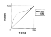
- 6 is a diagram illustrating a relationship between planned luminance and actual luminance in the liquid crystal display device according to Embodiment 2.
- FIG. 5 is a plan view showing a schematic configuration of a liquid crystal display device according to Embodiment 2.
- FIG. 6 is a plan view of a schematic configuration of two pixels adjacent in a column direction in a liquid crystal display device according to Embodiment 2.
- FIG. 6 is a diagram schematically illustrating a connection relationship between pixels and CS lines, a writing polarity of a source signal voltage, and an arrangement of sub-pixels in the liquid crystal display device according to the second embodiment.
- FIG. 10 is a diagram illustrating waveforms of signal voltages of two consecutive frames in the liquid crystal display device according to the second embodiment.
- FIG. 6 is a diagram illustrating waveforms of signal voltages of N frames and N + 1 frames in the liquid crystal display device according to the second embodiment.
- FIG. 10 is a diagram illustrating a writing polarity of a source signal voltage of each pixel of one frame in the liquid crystal display device according to the second embodiment.
- FIG. 10 is a diagram illustrating how pixels are scanned in N frames in the liquid crystal display device according to the second embodiment.
- FIG. 10 is a diagram showing how pixels are scanned in a subsequent subframe of N frames and a previous subframe of N + 1 frames in the liquid crystal display device according to the second embodiment. It is a figure which shows schematic structure of the liquid crystal display device which concerns on a modification. It is a figure which shows the specific pixel structure of the liquid crystal panel in the display part of the liquid crystal display device which concerns on a modification.
- (A)-(c) is a graph which shows the relationship between a gradation and the transmittance
- the liquid crystal display device (display device) according to the present embodiment performs display by dividing one frame into a plurality of (for example, two) sub-frames (frame division driving), and a plurality of (for example, a single pixel) Two sub-pixels are displayed with different luminances (pixel division driving and multi-pixel driving).
- pixel division driving pixel division driving and multi-pixel driving.
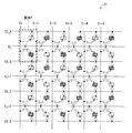
- the liquid crystal display device shown in FIG. 1 is arranged in a matrix (rp, cq) having a plurality of rows (1 to rp) and a plurality of columns (1 to cq), and each pixel P (p, q), ( However, 1 ⁇ p ⁇ rp, 1 ⁇ q ⁇ cq) includes two sub-pixels SPa (p, q) and SPb (p, q).
- FIG. 1 shows source lines (data signal lines) S-C1, S-C2, S-C3, S-C4,..., S-Ccq, gate lines (scanning signal lines) GL1, GL2.
- each pixel P (p, q), and sub-pixel SPa (p, A part (8 rows, 6 columns) of the relative arrangement of q) and SPb (p, q) is schematically shown.
- one pixel P (p, q) has subpixels SPa (p, q) and SPb (p, q) above and below a gate line G-Lp that horizontally penetrates the vicinity of the center of the pixel.
- the subpixels SPa (p, q) and SPb (p, q) are arranged in the column direction in each pixel.
- One of the storage capacitor electrodes (not shown) of each of the subpixels SPa (p, q) and SPb (p, q) is connected to the adjacent CS line CS-A or CS-B.
- a source line S-Cq for supplying a display signal (also referred to as “display signal voltage” or “source signal voltage”) corresponding to a display image to each pixel P (p, q) is provided between the pixels in the drawing.
- the sub-pixel (pixel) adjacent to the right of each source line is configured to supply a signal voltage to each TFT element (not shown).
- the configuration shown in FIG. 1 is a configuration in which one sub-pixel is shared by one CS line or one gate line, and has an advantage that the aperture ratio of the pixel can be increased.
- FIG. 2 is an equivalent circuit diagram of a certain region of the liquid crystal display device having the pixel arrangement shown in FIG.
- This liquid crystal display device has pixels arranged in a matrix having rows and columns, and each pixel has two sub-pixels.
- Each sub-pixel (the symbols A and B indicate two sub-pixels) has liquid crystal capacitors CLCA-n, m and CLCB-n, m and holding capacitors CCSA-n, m and CCSB-n, m. is doing.
- the liquid crystal capacitor includes a sub-pixel electrode, a counter electrode ComLC, and a liquid crystal layer provided therebetween.
- the storage capacitor includes a storage capacitor electrode, an insulating film, and a storage capacitor counter electrode (ComCSA-n, ComCSB- n).
- the two subpixels are connected to a common source line SBL-m via corresponding TFT-n, m and TFTB-n, m, respectively.
- the TFTA-n, m and the TFTB-n, m are controlled to be turned on / off by the scanning signal voltage supplied to the common gate line GBL-n, and when the two TFTs are in the on state, A display signal voltage is supplied from a common source line to the subpixel electrode and the storage capacitor electrode.
- One storage capacitor counter electrode of the two sub-pixels is connected to the storage capacitor trunk line (CS trunk line) CSVtypeR1 via the CS line (CSBL), and the other storage capacitor counter electrode is connected to the storage capacitor trunk line ( CS trunk line) connected to CSV type R2.
- CS lines corresponding to sub-pixels of pixels in adjacent rows in the column direction are electrically common to each other. Specifically, a CS line CSBL corresponding to n rows of sub-pixels CLCB-n, m and a CS line CSBL corresponding to sub-pixels CLCA-n + 1, m of pixels in a row adjacent in the column direction are electrically connected. This is a common point.
- FIGS. 3 and 4 show the cycle and phase of the CS voltage (CS signal) supplied to the CS line with reference to the voltage waveform of the gate line, and the voltage of each subpixel electrode.
- the liquid crystal display device reverses the direction of the electric field applied to the liquid crystal layer of each pixel at regular time intervals (for example, every vertical scanning period), so two types of drive voltage waveforms corresponding to the direction of each electric field. Need to think about. These two types of driving states are shown in FIGS. 3 and 4, respectively.
- VSBL-m represents a waveform of a display signal voltage (source signal voltage) supplied to m columns of source lines SBL-m
- VGBL-n and the like represent n rows of gate lines GBL-m.
- the waveform of the scanning voltage (gate signal voltage) supplied to n is shown
- VCSVtypeR1 and VCSVtypeR2 show the waveform of the CS voltage as the holding capacitor counter voltage supplied to the CS trunk line CSVtypeR1 and CSVtypeR2, respectively
- VPEA-m, n and VPEB-m, n indicates the voltage waveform of the liquid crystal capacitance of each subpixel.
- the first point to be noted is that the periods of the CSVtypeR1 and CSVtypeR1 voltages VCSVtypeR1 and VCSVtypeR2 are each one time (1H) of the horizontal scanning period.
- the second point to be noted in FIGS. 3 and 4 is that the phases of VCSVtypeR1 and VCSVtypeR2 are as follows. First, paying attention to the phase between the CS trunk lines, the phase of VCSVtypeR2 is delayed by 0.5H from VCSVtypeR1. Next, paying attention to the voltage of the CS main line and the voltage of the gate line, the phases of the voltage of the CS main line and the voltage of the gate line are as follows. 3 and 4, the time when the voltage of the gate line corresponding to each CS trunk line changes from VgH to VgL coincides with the time at the center of each flat portion of the CS trunk line voltage. That is, the value of Td shown in FIGS. 3 and 4 is 0.25 H hours. However, even in other cases, the Td value may be in a range larger than 0H and shorter than 0.5H time.
- the explanation regarding the period and phase of the voltage of the CS trunk line is based on FIG. 3 and FIG. 4, and the voltage waveform of the CS trunk line is not limited to this, and any one of the following two conditions may be satisfied.
- the first condition is that, after the voltage of any corresponding gate line changes from VgH to VgL, the first voltage change is a voltage increase, and VCSVtypeR2 has a voltage of any corresponding gate line from VgH. After changing to VgL, the first voltage change is a voltage decrease.
- the second condition is that VCSVtypeR1 changes the voltage of the corresponding arbitrary gate line from VgH to VgL, then the first voltage change is a voltage decrease, and VCSVtypeR2 determines that the voltage of the corresponding arbitrary gate line changes from VgH. After changing to VgL, the first voltage change is a voltage increase.
- FIG. 5 and 6 collectively show the driving state of the liquid crystal display device.
- the driving state of the liquid crystal display device is also shown separately in two cases where the polarity of the driving voltage of each sub-pixel is different as in FIGS.
- the driving state in FIG. 5 corresponds to the driving voltage waveform in FIG. 3
- the driving state in FIG. 6 corresponds to the driving voltage waveform in FIG.
- FIG. 5 and FIG. 6 schematically show driving states of pixels of (8 rows from n rows to n + 7 rows) ⁇ (6 columns from m columns to m + 5 columns) among a plurality of pixels arranged in a matrix.
- Each pixel has sub-pixels with different luminance levels, that is, sub-pixels marked “bright” and sub-pixels marked “dark”.
- one pixel is composed of two sub-pixels having different luminances, that is, a sub-pixel having a high luminance indicated as “bright” and a sub-pixel having a low luminance indicated as “dark”.
- the bright subpixels and dark subpixels are arranged in a checkered pattern.
- a set of display luminances (a set of display signal voltages) of two subframes corresponding to one frame is set so as to satisfy the following conditions.
- the first condition is that the average display luminance of the two subframes matches the luminance of the input video signal.
- the display luminance value of each frame corresponds to the luminance of the input video signal on a one-to-one basis
- Corresponding to the luminance of the input video signal is the average of the display luminance of the two sub-frames constituting each frame. That is, the integral value of the display luminance of the two subframes is set so as to correspond to the luminance of the input video signal.
- the second condition is that the display luminance of each subframe is set so that the difference in display luminance between the two subframes constituting one frame is different. As illustrated here, it is preferable to set the display brightness of each subframe so that the difference in display brightness between the two subframes is maximized. For example, in the case of the low luminance and the intermediate luminance in FIG. 7B, the display luminance of the previous subframe of the two subframes is set to the lowest luminance (black), and the display luminance of the subsequent subframe is set to the input video signal. The brightness is twice that of the brightness. In the high luminance and the maximum luminance of FIG.
- the rear subframe is set to the maximum luminance, and the difference in the luminance of the frame is represented by the display luminance value of the previous subframe.
- the luminance of the previous subframe of the two subframes is reduced, but conversely, the luminance of the subsequent subframe may be reduced.
- the previous sub-frame which occurs when the video signal is disturbed, such as a change in the vertical scanning period (V-Total) of the input video signal, is generated. This is preferable because an advantage that it is difficult to see the disturbance of the image at the beginning of writing can be obtained.
- one frame is divided into two subframes, but it may be divided into three or more subframes.
- the second condition can be rephrased as follows.
- the position of the subframe in the frame is a position on the time axis.
- both sides of the central subframe are both before and after the central subframe.
- the display brightness of the subframes on both sides need not be set symmetrically with respect to the central subframe.
- the polarity of the display signal voltage supplied to the source line is inverted at the frame period (period of one frame time width).
- One method is a method of applying a voltage having the same polarity for one frame.
- the other method is a method in which the display signal voltage is reversed between two subframes in one frame, and the subsequent subframe and the previous subframe of the next frame are driven with the same polarity. .
- FIG. 7 (a) shows the relationship between the voltage polarity (polarity of the voltage between electrodes) and the frame period when the former method is adopted.
- FIG. 7B shows the relationship between the voltage polarity and the frame period when the latter method is used.
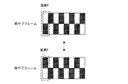
- each subpixel is arranged in a checkered pattern, and the brightness state of each subpixel is switched for each subframe (see FIG. 8). ).
- the source signal voltage written to each sub-pixel is different for each sub-frame.
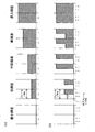
- Display example Here, an example of displaying a line-shaped image in the row direction in the liquid crystal display device will be described below.
- the bright subpixel is turned on from the 0th gradation to the 160th gradation, and the bright subpixel and the dark subpixel are turned on from the 160th gradation to the 255th gradation.
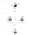
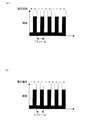
- FIG. 10A shows an image for four pixels corresponding to the input signal
- FIG. 10B shows a display state of the front subframe and the rear subframe
- FIG. 10C shows a display image of the display panel. Is shown.
- the first subpixel SP1 indicates 160 gradations
- the second subpixel SP2 indicates 0 gradations.
- the gradation of each subpixel is controlled by the bright subpixel of each subframe.
- signal voltages of 160 gradations and 0 gradations are alternately input to each source line, and 160 gradations and 0 gradations in the previous subframe and the subsequent subframe. The signal voltage is input so that and are reversed.
- a 160-gradation signal voltage is input to the source line where the first subpixel SP1 is a bright subpixel
- a 0-gradation signal voltage is input to the source line where the second subpixel SP2 is a bright subpixel.
- a line-like image can be displayed by the plurality of sub-pixels SP1 arranged in the row direction. That is, it is possible to independently control the luminance of each sub-pixel within one pixel. Therefore, an input signal having a vertical resolution twice that of the display panel can be displayed.
- a display quality corresponding to twice the vertical resolution (vertical resolution) as compared with the conventional liquid crystal display device Accordingly, for example, a high-resolution image (horizontal 1920 ⁇ vertical 2160) can be displayed on an FHD (horizontal 1920 ⁇ vertical 1080) liquid crystal panel.
- FIG. 11 schematically shows a combination of lighting states of the front subframe and the rear subframe with respect to a combination of subpixels to be displayed.
- FIG. 11 shows a combination of lighting states of the front subframe and the rear subframe with respect to a combination of subpixels to be displayed.
- FIG. 11 shows a combination of lighting states of the front subframe and the rear subframe with respect to a combination of subpixels to be displayed.
- FIG. 12 is a schematic diagram showing a schematic configuration of the liquid crystal display device according to the present embodiment.
- the liquid crystal display device includes a frame memory (FM) 11, a front stage LUT 12, a rear stage LUT 13, a display unit 14, and a control unit 15.
- FM frame memory
- the frame memory (image signal input unit) 11 stores an image signal (for example, RGB signal) input from an external signal source for one frame.
- the front-stage LUT (look-up table) 12 and the rear-stage LUT 13 are correspondence tables (conversion tables) between image signals input from the outside and display signals output to the display unit 14.
- the image signal has a resolution higher than that of the display panel 21.
- the liquid crystal display device performs display by two subframes having the same size (period) at twice the frequency based on an image signal for one frame input in one frame period.
- the number of subframes is not limited to two, and may be three or more. That is, the liquid crystal display device performs display by dividing one frame into a plurality of (m (m: integer of 2 or more)) subframes.
- the front LUT 12 is a correspondence table for display signals (previous display signals) output in the previous subframe (previous subframe).
- the rear-stage LUT 13 is a correspondence table for display signals (rear-stage display signals) output in the rear-stage subframe (rear-stage subframe).
- the display unit 14 includes a liquid crystal panel 21, a gate driver (scanning signal line driving circuit) 22, a source driver (data signal line driving circuit) 23, and a CS driver (holding capacity wiring driving circuit) 24.
- An image is displayed based on the input display signal.
- the liquid crystal panel 21 has a pixel division structure (multi-pixel structure). Specifically, the liquid crystal panel 21 includes a first subpixel and a second subpixel in which each of a plurality of pixels arranged in the row direction and the column direction (matrix shape) displays different luminances at least in a certain gradation.
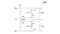
- FIG. 13 is an equivalent circuit diagram showing one pixel P of the liquid crystal panel 21
- FIG. 14 is a plan view showing a connection relation of a part of the liquid crystal panel 21
- FIG. 15 is a part of the liquid crystal panel 21. It is a top view which shows typically the display state of.
- the pixel P includes a first subpixel electrode 51a and a second subpixel electrode 51b.
- the first subpixel electrode 51a is connected to the gate line 52 and the source line 54 via the first transistor 56a.
- the second subpixel electrode 51b is connected to the gate line 52 and the source line 54 via the second transistor 56b.
- a first liquid crystal capacitor Clc1 is formed between the first subpixel electrode 51a and the counter electrode com, and a second liquid crystal capacitor Clc2 is formed between the second subpixel electrode 51b and the counter electrode com.
- a first storage capacitor CS1 is formed between the first subpixel electrode 51a and the first CS line (first storage capacitor line) 53a, and the second subpixel electrode 51b and the second CS line (second storage capacitor line) 53b. Is formed with a second storage capacitor CS2.
- a source signal voltage (display signal voltage) is supplied from the common source line 54 to the first subpixel electrode 51a and the second subpixel electrode 51b, and then the transistors 56a and 56b are turned off.
- the voltages (retention capacitor wiring signals) of the 1CS line 53a and the second CS line 53b are changed (level shifted) to be different from each other.
- the voltages applied to the first liquid crystal capacitor Clc1 and the second liquid crystal capacitor Clc2 are different from each other, and a bright sub-pixel having a relatively high brightness and a darkness having a relatively low brightness are included in one pixel.
- Sub-pixels are formed.
- a specific configuration example of a liquid crystal display device in which a bright subpixel and a dark subpixel are formed in one pixel will be described later.
- the bright sub-pixels and the dark sub-pixels are arranged in a checkered pattern.
- the control unit 15 is a central part of the liquid crystal display device that controls all operations in the liquid crystal display device. Then, the control unit 15 generates a display signal from the image signal stored in the frame memory 11 using the front-stage LUT 12 and the rear-stage LUT 13 and outputs the display signal to the display unit 14.
- control unit 15 stores an image signal transmitted at a normal output frequency (normal clock; for example, 25 MHz) in the frame memory 11. Then, the control unit 15 outputs the image signal from the frame memory 11 twice by a clock having a frequency twice that of the normal clock (double clock; 50 MHz).
- a normal output frequency normal clock; for example, 25 MHz
- double clock twice that of the normal clock
- control part 15 produces
- control unit 15 changes the pixel potential written to each sub-pixel electrode by changing (level shifting) the voltage level of the CS signal supplied to the first CS line 53a and the second CS line 53b. Sub-pixels and dark sub-pixels are formed.
- the display unit 14 displays different images once in one frame period based on two display signals that are sequentially input (all gate lines of the liquid crystal panel 21 are displayed as one in both subframe periods). At the same time, in each subframe, an image with bright subpixels and dark subpixels is displayed. A specific output operation of the display signal will be described later.
- a method of generating the front display signal and the rear display signal by the control unit 15 will be described.
- general display brightness the brightness of an image displayed on the panel
- the liquid crystal panel the display of an image displayed on the panel
- the luminance gradation (signal gradation) is in a range from 0 to 255.
- the signal gradation and display luminance in the liquid crystal panel are approximately expressed by the following equation (1).
- L is a signal gradation (frame gradation) when an image is displayed in one frame (when an image is displayed in normal hold display)
- Lmax is a maximum luminance gradation (255)
- T is a display luminance
- ⁇ is a correction value (normally 2.2).
- the display brightness T output from the liquid crystal panel 21 is shown as a graph in FIG.
- “brightness to be output (scheduled luminance; value corresponding to signal gradation, equivalent to the above display luminance T)” is plotted on the horizontal axis, and “brightness actually output (actual luminance is plotted on the vertical axis). ) ”.
- the above two luminances are equal on the front surface (viewing angle 0 degree) of the liquid crystal panel 21.
- the viewing angle is set to 60 degrees, the actual brightness becomes brighter at a halftone brightness due to a change in the gradation ⁇ characteristic.
- the control unit 15 performs the following for each subpixel.
- control unit 15 is designed so that the frame is evenly divided into two subframes and the luminance up to half of the maximum luminance is displayed by one subframe.
- the control unit 15 sets the previous subframe to the minimum luminance (black) and sets the subsequent subframe.
- the gradation expression is performed by adjusting only the display luminance of (the gradation expression is performed using only the subsequent subframe).
- the integrated luminance in one frame is “(minimum luminance + brightness of subsequent subframe) / 2”.
- the control unit 15 sets the rear subframe to the maximum luminance (white), and adjusts the display luminance of the previous subframe to express the gradation expression. Do. In this case, the integrated luminance in one frame is “(luminance of the previous subframe + maximum luminance) / 2”.
- the signal gradation setting is performed by the control unit 15.
- the control unit 15 obtains the frame gradation L based on the image signal output from the frame memory 11 when displaying the image.
- L is equal to or less than Lt
- the control unit 15 sets the luminance gradation (F) of the previous display signal to the minimum (0) by the previous LUT 12.
- the control unit 15 sets the luminance gradation R of the subsequent display signal to the maximum (255).
- control unit 15 sets the luminance gradation F of the previous subframe based on the expression (1).
- F (L ⁇ ⁇ 0.5 ⁇ Lmax ⁇ ⁇ ) ⁇ (1 / ⁇ ) (4)
- the number of pixels of the liquid crystal panel 21 is a ⁇ b.
- the control unit 15 accumulates the previous stage display signal of the pixel (a number) of the first gate line with respect to the source driver 23 with a double clock.
- control unit 15 turns on the first gate line by the gate driver 22 and writes the previous stage display signal to the pixels of this gate line. Thereafter, the control unit 15 similarly turns on the second to b-th gate lines with a double clock while changing the previous display signal stored in the source driver 23. As a result, the previous stage display signal can be written to all the pixels in a half period of one frame (1/2 frame period).
- control unit 15 performs the same operation, and writes the subsequent display signal to the pixels of all the gate lines in the remaining half frame period.
- the front display signal and the rear display signal are written into each pixel by equal time (1/2 frame period).
- control unit 15 sequentially turns on the odd-numbered gate lines in the first quarter frame period, and then turns on the odd number in the second quarter frame period. All gate lines are selected by sequentially turning on the gate lines in the row.
- FIG. 17 shows the result (broken line and solid line) of the subframe display that outputs the preceding stage display signal and the rear stage display signal divided into the front and rear subframes (broken line and solid line), and the result shown in FIG. ).
- the deviation between the actual luminance at a large viewing angle and the planned luminance is minimum (0) when the display luminance is minimum or maximum, while it is halftone (near the threshold luminance).
- the largest liquid crystal panel 21 is used.
- subframe display is performed in which one frame is divided into subframes. Furthermore, the period of the two subframes is set to be equal, and in the case of low luminance, the previous subframe is displayed in black and display is performed using only the rear subframe within a range in which the integrated luminance in one frame is not changed. Accordingly, since the shift in the previous subframe is minimized, the total shift in both subframes can be reduced to about half as shown by the broken line in FIG.
- the display is performed by adjusting the luminance of only the previous sub-frame, with the subsequent sub-frame displaying white within a range in which the integrated luminance in one frame is not changed. For this reason, also in this case, since the shift of the subsequent subframe is minimized, the total shift of both subframes can be reduced to about half as shown by the broken line in FIG.
- the liquid crystal display device it is possible to reduce the overall displacement by about half compared to a configuration in which normal hold display is performed (a configuration in which an image is displayed in one frame without using a subframe). ing. For this reason, it is possible to suppress the phenomenon that the halftone image becomes bright and floats white as shown in FIG.
- the periods of the previous subframe and the subsequent subframe are equal. This is because the luminance up to half of the maximum value is displayed in one subframe. However, these subframe periods may be set to different values.
- the liquid crystal panel 21 is preferably driven by alternating current in order to prevent so-called burn-in.
- the liquid crystal display device varies the voltage value (absolute value) applied between the pixel electrodes between subframes. Therefore, when the polarity of the interelectrode voltage is inverted in the subframe period, the applied interelectrode voltage is biased due to the difference in voltage value between the previous subframe and the subsequent subframe. For this reason, when the liquid crystal panel 21 is driven for a long time, electric charges accumulate on the electrodes, which may cause image sticking or flicker.
- the polarity of the voltage between the electrodes is reversed with a frame period (period of one frame time width).
- One method is a method of applying a voltage having the same polarity for one frame.
- the interelectrode voltage is reversed between two subframes in one frame, and the subsequent subframe and the previous subframe of the next frame are driven with the same polarity. It is.
- FIG. 18 (a) shows the relationship between the voltage polarity (polarity of the voltage between electrodes) and the frame period when the former method is adopted.
- FIG. 18B shows the relationship between the voltage polarity and the frame period when the latter method is used.
- the liquid crystal panel 21 is driven by sub-frame display, thereby suppressing whitening.
- the response speed of the liquid crystal the speed until the voltage applied to the liquid crystal (voltage between electrodes) becomes equal to the applied voltage
- the effect of such subframe display may be diminished. That is, when performing normal hold display, in the TFT liquid crystal panel, one liquid crystal state corresponds to a certain luminance gradation. Therefore, the response characteristics of the liquid crystal do not depend on the luminance gradation of the display signal.
- the relationship between the planned brightness and the actual brightness is as shown in FIG. That is, even when subframe display is performed, it is impossible to perform display with luminance (minimum luminance / maximum luminance) in which the difference (shift) between the planned luminance and the actual luminance when the viewing angle is large is small. For this reason, the effect of suppressing the whitening phenomenon is reduced.
- the liquid crystal response speed in the liquid crystal panel 21 is designed so as to satisfy the following (c) and (d).
- (c) A voltage signal (generated by the source driver 23 based on the display signal) for achieving the maximum luminance (white; equivalent to the maximum brightness) on the liquid crystal displaying the minimum luminance (black; equivalent to the minimum brightness). ),
- the voltage of the liquid crystal (interelectrode voltage) reaches a value of 90% or more in the voltage signal voltage within the shorter subframe period (the actual brightness of the front is 90% of the maximum brightness).
- the previous subframe when the luminance is low, the previous subframe is black, and gradation expression is performed using only the rear subframe.
- the same display can be obtained even if the context of the subframes is exchanged (even if the subsequent subframe is black in the case of low luminance and the gradation representation is performed using only the previous subframe).
- the luminance gradation (signal gradation) of the display signal (the front display signal and the rear display signal) is set using the equation (1).
- the actual panel has luminance even in the case of black display (gradation 0) and the response speed of the liquid crystal is finite. Therefore, it is preferable to take these factors into consideration when setting the signal gradation. .
- ⁇ 2.2 is set in accordance with the input signal gradation (luminance gradation of the display signal) (1) A voltage signal is output to each pixel (liquid crystal) so that the display luminance obtained using can be obtained.
- Such a source driver 23 outputs the voltage signal used in the normal hold display as it is in each subframe in accordance with the input signal gradation even when performing the subframe display.
- the sum of the luminance in one frame in the sub-frame display may not be the same as the value in the normal hold display (the signal gradation cannot be expressed).
- the source driver 23 is preferably designed to output a voltage signal converted into divided luminance. That is, it is preferable that the source driver 23 is set so as to finely adjust the voltage (interelectrode voltage) applied to the liquid crystal according to the signal gradation. For this reason, it is preferable to design the source driver 23 for subframe display so that the fine adjustment as described above can be performed.
- the liquid crystal panel 21 is a VA panel.
- the present invention is not limited to this, and even when a liquid crystal panel of a mode other than the VA mode is used, the white-out phenomenon can be suppressed by the sub-frame display of the liquid crystal display device.
- the sub-frame display of the liquid crystal display device is a liquid crystal panel in which the planned brightness (scheduled brightness) and the actual brightness (actual brightness) deviate when the viewing angle is increased (the mode in which the viewing angle characteristics of the gradation gamma change).
- the sub-frame display of the liquid crystal display device is effective for a liquid crystal panel having a characteristic that the display luminance increases as the viewing angle is increased.
- liquid crystal panel 21 in the liquid crystal display device may be NB (Normally Black) or NW (Normally White).
- another display panel for example, an organic EL panel or a plasma display panel
- an organic EL panel or a plasma display panel instead of the liquid crystal panel 21, another display panel (for example, an organic EL panel or a plasma display panel) may be used.
- the frame may be designed to be divided within a range of 1: n or n: 1 (n is a natural number of 1 or more).
- the liquid crystal display device performs pixel division driving (multi-pixel driving) in addition to the above-described frame division driving (sub-frame display). Next, a configuration example of a pixel division structure (multi-pixel structure) will be described.
- FIG. 21 is a plan view showing a schematic configuration of the liquid crystal display device
- FIG. 22 is a plan view showing a schematic configuration of two pixels adjacent in the column direction. The equivalent circuit of each pixel is as shown in FIG.
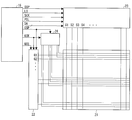
- the liquid crystal display device includes a liquid crystal panel 21, a source driver 23 (data signal line driving circuit) for supplying a source signal voltage to source lines (data signal lines) S 1.
- a gate driver 22 (scanning signal line driving circuit) for supplying a gate signal voltage to the lines (scanning signal lines) G1...
- a CS voltage (holding capacity wiring signal) to the CS lines (holding capacity wiring) CS1.
- a CS driver 24 to be supplied, a source driver 23, a gate driver 22, and a control unit 15 that controls the CS driver 24 are provided.
- Each pixel of the liquid crystal panel 21 has two subpixels.
- the first subpixel SP-1 in FIG. 22 has the first liquid crystal capacitor Clc1 and the first holding capacitor CS1 shown in FIG. 13, and the second subpixel SP-2 in FIG. 22 has the second liquid crystal shown in FIG. It has a capacity Clc2 and a second holding capacity CS2.
- the first liquid crystal capacitor Clc1 is formed by the first subpixel electrode 51a, the counter electrode com, and the liquid crystal layer therebetween
- the second liquid crystal capacitor Clc2 is formed by the second subpixel electrode 51b
- the counter electrode com is formed by a liquid crystal layer between them.
- the counter electrode com is provided in common to the two subpixels, and is generally provided in common to all the pixels in the display area. However, a large liquid crystal panel may be divided into a plurality of regions.
- the control unit 15 represents a data start pulse signal SSP, a data clock signal SCK, a latch strobe signal LS, a signal POL for controlling the polarity of the data signal, and an image to be displayed as signals to be displayed on the liquid crystal panel 21.
- a digital image signal DA, a gate start pulse signal GSP, a gate clock signal GCK, and a gate driver output control signal GOE are generated and output.
- the digital image signal DA, the latch strobe signal LS, the signal POL for controlling the polarity of the data signal, the data start pulse signal SSP and the data clock signal SCK are input to the source driver 23, and the gate start pulse signal GSP, the gate clock signal GCK and The gate driver output control signal GOE is input to the gate driver 22.
- the source driver 23 is an image represented by the digital image signal DA based on the digital image signal DA, the data start pulse signal SSP, the data clock signal SCK, the latch strobe signal LS, and the signal POL for controlling the polarity of the data signal (display signal voltage).
- a data signal is sequentially generated for each horizontal scanning period as an analog voltage corresponding to the pixel value in each horizontal scanning period, and these data signals are respectively applied to the source line Si.
- the CS driver 24 receives the gate clock signal GCK and the gate start pulse signal GSP.
- the CS driver 24 controls the waveform of the CS voltage.
- the liquid crystal display device performs multi-pixel driving as described above. That is, as shown in FIG. 13, a source signal voltage (display signal voltage) is supplied from a common source line 54 to the first subpixel electrode 51a and the second subpixel electrode 51b, and then each transistor 56a, After the 56b is turned off, the voltages of the first CS line 53a and the second CS line 53b are changed (level shifted) so as to be different from each other. Accordingly, the voltages applied to the first liquid crystal capacitor Clc1 and the second liquid crystal capacitor Clc2 are different, and a bright subpixel and a dark subpixel are formed in one pixel. In this configuration, since the source signal voltage is supplied from one source line to the two subpixel electrodes, there is an advantage that it is not necessary to increase the number of source lines and the number of source drivers that drive them.
- a source line inversion driving method is applied to multi-pixel driving, and gate line interlaced scanning driving (interlace driving) is performed.
- interlace driving gate line interlaced scanning driving
- the power consumption of the source driver that is, heat generation
- the driving method of the liquid crystal display device is not limited to this.
- odd-numbered rows are scanned first (even-numbered rows are interlaced), and then even-numbered rows are scanned. It goes without saying that even rows may be scanned first (skipping over odd rows) and then odd rows may be scanned.
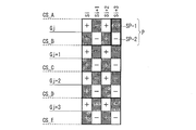
- FIG. 23 schematically shows the connection relationship between the pixels of the liquid crystal display device and the CS line, and also shows the source signal voltage writing polarity (+ ⁇ in the figure) and two bright and dark sub-pixels (hatching in the figure is dark and dark).
- 2 is a diagram schematically showing the arrangement of pixels), and shows a state in which source line inversion driving is performed.
- Gj to Gj + 3 are gate lines
- CS-A to CS-E are CS lines
- Si to Si + 3 are source lines.
- the bright subpixels and the dark subpixels are arranged in a checkered pattern while the writing polarity for each column is constant.
- the connection relationship between the pixels indicating the bright sub-pixel and the dark sub-pixel is as shown in FIG.
- FIG. 24 shows the waveform of each signal voltage in the liquid crystal display device for two consecutive frames (arbitrary N frames, N + 1 frames).
- Vcom in the figure indicates a counter voltage.
- FIG. 25 shows the waveform of each signal voltage in the liquid crystal display device for the N frame and the N + 1 frame.
- the CS voltage Vcs-B supplied from the CS line CS-B and the i-th source line Si are sequentially shown from the top.
- a voltage Vp-B (ij) applied to the sub-pixel PB (i, j) having a storage capacitor connected to the CS line CS-B is shown.
- FIG. 26 shows the writing polarity of the source signal voltage of each pixel in one frame (arbitrary N frame; previous subframe and rear subframe).
- the source line inversion driving and the gate line interlaced scanning driving are performed. Therefore, in FIG. 26, each subframe is divided into two periods (divided subframes; 1 division subframe period) and the latter half quarter frame (second division subframe period)).
- FIG. 27 is a diagram illustrating how pixels are scanned in an N frame.
- the source signal voltage supplied to the i-th source line Si and the gates from the first row to the n-th row are shown in FIG.
- the waveform of the gate signal voltage supplied to the lines G1 to Gn is schematically shown. Also in this figure, each sub-frame is divided into two periods (first quarter frame and second quarter frame).
- the pixel data write pulse Pw at which the gate signal voltage Vgj changes from VgL (low level) to VgH (high level) for a certain period from the gate line Gj of odd rows. are sequentially applied. That is, the source signal voltage is written to all the odd-numbered pixels from the first row to the (n ⁇ 1) th row.
- the pixel data write pulse Pw in which Vgj changes from VgL to VgH for a certain period of time is sequentially applied to the even-numbered gate line Gj + 1. That is, the source signal voltage is written in all even-numbered pixels from the second row to the n-th row.
- the polarity of the source signal voltage supplied to the source line Si is a positive source signal voltage (Vsp) with respect to the median value Vsc (generally approximately equal to Vcom) of the source signal voltage in the first quarter frame.
- Vsp positive source signal voltage
- the positive source signal voltage is also applied in the next second quarter frame.
- the positive source signal voltage is also applied to the first half frame and the last quarter frame of the N subframes.
- a negative source signal voltage (Vsn) is applied to Vsc, and in the next subsequent subframe, a negative source signal voltage is applied.
- the source signal voltage supplied to Si + 1 adjacent to the source line Si has a polarity opposite to that of the source signal voltage supplied to the source line Si.
- the source signal voltage supplied to the source line Si + 2 has a polarity opposite to that of the source signal voltage supplied to the source line Si + 1.
- the CS voltage Vcs-A supplied to the CS line CS-A has a waveform whose polarity is inverted with respect to the counter electrode voltage Vcom at a constant cycle (for example, a rectangular wave having a duty ratio of 1: 1 as shown in the figure). have.
- the CS voltage Vcs-A supplied to the line CS-A has a waveform whose polarity is inverted with respect to the counter electrode voltage Vcom at a constant cycle (for example, a rectangular wave having a duty ratio of 1: 1 as shown in the figure).
- the first change (level shift) of the CS voltage Vcs-A of the CS line CS-A after the gate signal voltage of the gate line Gj becomes low is increased (for example, in this case, from negative polarity to positive polarity).
- the voltage of the subpixel PA (i, j) rises due to the push-up action, and the effective voltage applied to the subpixel PA (i, j) is written by Pw. It becomes equal to or higher than the source signal voltage (absolute value increases), and the subpixel PA (i, j) becomes a bright subpixel (see FIG. 24).
- the voltage of the sub-pixel PB (i, j) is also written with a positive polarity. Since the first change (level shift) of the CS voltage of the CS line CS-B after the gate signal voltage of the gate line Gj becomes low is a drop (for example, change from positive polarity to negative polarity in this case), the subpixel The voltage of PB (i, j) drops due to the push-down action, and the effective voltage applied to the sub-pixel PB (i, j) is less than or equal to the source signal voltage written by Pw (absolute The value becomes smaller), and the sub-pixel PB (i, j) becomes a dark sub-pixel (see FIG. 25).
- the polarities are opposite to each other.
- the CS voltage increases or decreases the effective voltage of the subpixel PA (i, j) connected to the gate line Gj selected in the previous subframe period in one frame, and the subsequent It has a waveform in which the action of raising or lowering the effective voltage of the subpixel PA (i, j) connected to the gate line Gj selected between the subframes is opposite to each other.
- the above-described advantage of the source inversion driving method can be obtained, and the display quality such as a feeling of roughness can be reduced without breaking the checkered pattern distribution of the bright pixels and the dark pixels. Can be prevented.
- FIG. 28 shows signal voltage waveforms of a plurality of even-numbered rows (j + 1 rows) skipped in the first quarter frame in the last quarter frame. As shown in FIG. 28, the polarity and the light / dark state of the subpixel PB (i, j + 1) are switched in the same manner as the subpixel PA (i, j).
- FIG. 29 shows the writing polarity of the source signal voltage of each pixel in the subsequent subframe of N frames and the previous subframe of N + 1 frames.
- FIG. 30 is a diagram showing how pixels are scanned in the subsequent subframe of the N frame and the previous subframe of the N + 1 frame, and the source signal supplied to the i-th source line Si. The waveforms of the voltage and the gate signal voltage supplied to the gate lines G1 to Gn from the first row to the n-th row are schematically shown. In this way, the polarity of the source signal voltage is inverted at the frame period (period of one frame time width).
- each subpixel is arranged in a checkered pattern, and the brightness state of each subpixel is switched for each subframe (see FIG. 33). ).
- the source signal voltage written to each sub-pixel is different for each sub-frame.
- the liquid crystal display device can also realize a display quality corresponding to twice the vertical resolution (vertical resolution) as compared with the conventional liquid crystal display device. Accordingly, for example, a high-resolution image (horizontal 1920 ⁇ vertical 2160) can be displayed on an FHD (horizontal 1920 ⁇ vertical 1080) liquid crystal panel.
- liquid crystal display devices according to the first and second embodiments can be applied to, for example, the multi-primary color display device described in “WO 2011/102343”.
- one display pixel may be configured by three types of subpixels of red, green, and blue, or may be configured by four or more types of subpixels.
- a liquid crystal display device in which one display pixel includes four types of sub-pixels of red, green, blue, and yellow will be described.
- FIG. 31 shows a liquid crystal display device according to a modification.
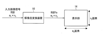
- the liquid crystal display device includes a resolution conversion device 10 (corresponding to the control unit 15 in FIG. 12) and a display unit 14, and is a multi-primary color display device that performs display using four primary colors. .
- FIG. 32 shows a specific pixel structure (sub-pixel arrangement) of the liquid crystal panel 21 in the display unit 14.
- each of the plurality of pixels P includes four types of sub-pixels that display different colors.
- the four types of subpixels are a red subpixel R that displays red, a green subpixel G that displays green, a blue subpixel B that displays blue, and a yellow subpixel Ye that displays yellow.
- these four types of subpixels are arranged in one row and four columns.
- Each of the four types of subpixels is composed of a bright subpixel and a dark subpixel.
- the total number of the plurality of pixels P of the liquid crystal panel is referred to as “display resolution” unless otherwise specified.
- the display resolution when m pixels P are arranged in the row direction and n pixels in the column direction is expressed as “m ⁇ n”.
- the minimum display unit of the input image is also called “pixel”, and the total number of pixels of the input image is called “resolution of the input image”.
- the resolution of an input image composed of m pixels in the row direction and n pixels in the column direction is expressed as “m ⁇ n”.
- the resolution conversion apparatus 10 shown in FIG. 31 converts the resolution (m1 ⁇ n1) of the image signal input from the outside so as to match the display resolution (m2 ⁇ n2) of the display unit 14. Further, the resolution conversion apparatus 10 displays image signals corresponding to the three primary colors (red, green, and blue) in the four primary colors (red subpixel R, green subpixel G, blue subpixel B, and yellow subpixel). , Red, green, blue, and yellow).
- each of the plurality of pixels P has a sub-pixel that displays the color with the highest luminance among the four types of sub-pixels (referred to as a “first sub-pixel” for convenience) and the second luminance.
- first sub-pixel for convenience
- second subpixel for convenience
- FIG. 32 shows an example of subpixel arrangement when the first subpixel is the green subpixel G and the second subpixel is the yellow subpixel. In the example shown in FIG.
- each pixel P the four types of subpixels are arranged in the order of the red subpixel R, the green subpixel G, the blue subpixel B, and the yellow subpixel Ye from the left side to the right side.
- the green subpixel G and the yellow subpixel Ye are not adjacent to each other.
- the liquid crystal display device when the resolution of the input image is higher than the display resolution (that is, when the total number of pixels of the input image is larger than the total number of the plurality of pixels P of the liquid crystal panel), each of the plurality of display units is changed. Display can be performed as virtual pixels. Therefore, visual resolution can be improved in the horizontal direction. Further, the liquid crystal display device displays a color with the highest luminance (that is, the highest luminance at the highest gradation) and a color with the second highest luminance (that is, the luminance at the highest gradation is 2).
- (Second highest) second subpixel is arranged so as not to be adjacent in the pixel P, so that the luminance distribution is higher than that in the case where the first subpixel and the second subpixel are arranged adjacent to each other. It is possible to increase the spatial frequency and prevent two adjacent virtual pixels from being merged and viewed.
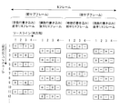
- FIG. 33 schematically shows a state of change in brightness of each subpixel for each subframe in two consecutive frames.
- the positive polarity and the negative polarity indicate the polarity of the signal voltage supplied to each source line
- the up and down arrows indicate how the CS voltage changes after the gate signal voltage goes low. Show.
- the gray color in FIG. 33 indicates a dark sub-pixel.
- liquid crystal display device it is possible to independently control the luminance of each sub-pixel within one pixel. Therefore, according to the liquid crystal display device according to the present modification, it is possible to realize display quality corresponding to twice the vertical resolution (vertical resolution) and the horizontal resolution (horizontal resolution). Thereby, for example, in an FHD (horizontal 1920 ⁇ vertical 1080) liquid crystal panel, an image (horizontal 3840 ⁇ vertical 2160) corresponding to a 4K2K panel (ultra high definition liquid crystal panel) can be displayed.
- FHD horizontal 1920 ⁇ vertical 1080
- 4K2K panel ultra high definition liquid crystal panel
- the amplitude of the CS voltage is determined so that the lighting of the dark sub-pixel is started before the bright sub-pixel becomes brightest.
- FIG. 34 is a graph showing the relationship between the gradation and the transmittance of each sub-pixel (PS1, PS2) according to the CS voltage. As shown in this graph, in the CS voltage corresponding to the wide viewing angle (graph indicated by A0), the dark sub-pixel starts to light before the bright sub-pixel becomes completely white near the 160th gradation. This can be understood (see FIGS. 34A and 34B).
- the present invention can be suitably used for various electronic devices such as a liquid crystal television.
Landscapes
- Engineering & Computer Science (AREA)
- Physics & Mathematics (AREA)
- Computer Hardware Design (AREA)
- General Physics & Mathematics (AREA)
- Theoretical Computer Science (AREA)
- Chemical & Material Sciences (AREA)
- Crystallography & Structural Chemistry (AREA)
- Power Engineering (AREA)
- Liquid Crystal Display Device Control (AREA)
- Control Of Indicators Other Than Cathode Ray Tubes (AREA)
- Liquid Crystal (AREA)
Abstract
表示パネルの解像度よりも高い解像度を有する入力画像を、表示品位を低下させることなく表示することが可能な表示装置および表示方法を提供する。1フレームを2個のサブフレームに分割して画像表示を行う表示装置であって、各画素の明副画素および暗副画素それぞれがサブフレームごとに入れ替わり、入力信号は表示パネルの2倍の垂直解像度を有し、各画素に供給する電圧をサブフレームごとに異ならせることにより入力信号に応じた画像を表示する。
Description
本発明は、表示パネルの解像度とは異なる解像度を有する入力画像データの表示を行う表示装置に関するものである。
従来の表示装置は、入力された画像データの解像度が表示パネルの解像度とは異なる場合、入力画像を拡大または縮小して表示している(例えば特許文献1)。つまり、入力画像の画素数が表示パネルの総画素数とは異なる場合、表示パネルでは入力画像の画素数とは異なる画素数で表示が行われる。
入力画像の拡大・縮小の手法としては、バイリニア法やバイキュービック法等が知られている。これらの手法では、入力画像に存在しない画素について周囲の画素の値から平均または加重平均により補間したり、フィルタ処理のような演算を用い、入力画像の画素を間引いたりすることで、表示パネルの画素に対応する出力値を求めて表示を行っている。
しかし、従来の手法により入力画像に対して拡大・縮小処理を行うと、元の入力画像データに含まれる輪郭や色などの情報を完全に再現することはできない。例えば、入力画像を縮小する場合は、出力側の解像度(表示パネルの総画素数)に依存して画素数が減少するので、色のにじみなどが発生して画質の低下を招いてしまう。
一般に、縮小処理を行う場合、入力信号にローパスフィルタ(LPF)処理を施した後に出力側(表示パネル側)の解像度に従ってサンプリング処理を行う。LPFの遮断特性は、出力側で表示可能な周波数の最大値の1/2を目安として設計される。このLPFの特性により、縮小後の画像にはぼやけや歪みが発生する。これらのぼやけや歪みは原理的なものであり、従来の手法では回避することはできない。
本発明は、上記問題に鑑みてなされたものであり、その目的は、表示パネルの解像度よりも高い解像度を有する入力画像を、表示品位を低下させることなく表示することが可能な表示装置および表示方法を提供することにある。
本発明に係る表示装置は、上記課題を解決するために、
1フレームを、m個(m;2以上の整数)のサブフレームに分割して画像表示を行う表示装置であって、
表示部の各画素が、互いに輝度が異なる第1副画素および第2副画素を有しており、
各画素において、上記第1副画素および上記第2副画素それぞれが、高輝度および低輝度の画像を上記サブフレームごとに入れ替えて表示し、
外部から当該表示装置に入力される入力信号は、垂直解像度が表示パネルの垂直解像度とは異なっており、
各画素に供給する電圧を上記サブフレームごとに異ならせることにより、上記入力信号に応じた画像を表示することを特徴とする。
1フレームを、m個(m;2以上の整数)のサブフレームに分割して画像表示を行う表示装置であって、
表示部の各画素が、互いに輝度が異なる第1副画素および第2副画素を有しており、
各画素において、上記第1副画素および上記第2副画素それぞれが、高輝度および低輝度の画像を上記サブフレームごとに入れ替えて表示し、
外部から当該表示装置に入力される入力信号は、垂直解像度が表示パネルの垂直解像度とは異なっており、
各画素に供給する電圧を上記サブフレームごとに異ならせることにより、上記入力信号に応じた画像を表示することを特徴とする。
上記構成によれば、表示装置は、いわゆるフレーム分割駆動および画素分割駆動を行う。また、上記表示装置では、各画素において、第1副画素および第2副画素それぞれの明暗の表示状態が、サブフレームごとに入れ替わるとともに、各画素に供給される電圧がサブフレームごとに異なっている。これにより、第1副画素および第2副画素それぞれを独立に輝度制御することができる。そのため、例えば1画素が2つの副画素で構成され、1フレームを2個のサブフレームに分割して表示する場合、表示パネルの縦解像度の2倍の縦解像度を有する入力信号を表示することができる。
よって、上記表示装置によれば、表示パネルの解像度よりも高い解像度を有する入力画像を、表示品位を低下させることなく表示することができる。
本発明に係る表示装置では、
第1~第mサブフレームの表示信号を上記表示部に出力する制御部とを備えており、
上記第1副画素および上記第2副画素は、同一のデータ信号線および同一の走査信号線に接続されているとともに、互いに異なる保持容量配線に接続されており、
上記制御部は、上記第1副画素に対応する保持容量配線に供給する保持容量配線信号と、上記第2副画素に対応する保持容量配線に供給する保持容量配線信号とを、互いに異なる方向にレベルシフトするとともに、それぞれについて1フレーム内でレベルシフトの方向を変更し、かつ、表示信号の電圧極性をフレーム周期で反転するとともに、該表示信号の電圧を上記サブフレームごとに異ならせることにより、上記第1副画素と上記第2副画素とに輝度差を与えることが好ましい。
第1~第mサブフレームの表示信号を上記表示部に出力する制御部とを備えており、
上記第1副画素および上記第2副画素は、同一のデータ信号線および同一の走査信号線に接続されているとともに、互いに異なる保持容量配線に接続されており、
上記制御部は、上記第1副画素に対応する保持容量配線に供給する保持容量配線信号と、上記第2副画素に対応する保持容量配線に供給する保持容量配線信号とを、互いに異なる方向にレベルシフトするとともに、それぞれについて1フレーム内でレベルシフトの方向を変更し、かつ、表示信号の電圧極性をフレーム周期で反転するとともに、該表示信号の電圧を上記サブフレームごとに異ならせることにより、上記第1副画素と上記第2副画素とに輝度差を与えることが好ましい。
上記構成によれば、保持容量配線に供給する保持容量配線信号の電圧レベルをシフトすることにより、各画素において、明副画素および暗副画素を形成することができる。
本発明に係る表示装置では、
1フレームは、2個のサブフレームに分割され、
上記第1副画素および上記第2副画素は、それぞれが行方向に並んで配されているとともに、列方向に交互に配されており、
上記入力信号は、垂直解像度が上記表示パネルの垂直解像度の2倍であることが好ましい。
1フレームは、2個のサブフレームに分割され、
上記第1副画素および上記第2副画素は、それぞれが行方向に並んで配されているとともに、列方向に交互に配されており、
上記入力信号は、垂直解像度が上記表示パネルの垂直解像度の2倍であることが好ましい。
これにより、例えば、FHD(横1920×縦1080)の液晶パネルにおいて、高解像度の画像(横1920×縦2160)を表示することができる。
本発明に係る表示装置では、
1フレームを2つのサブフレームに分割する場合、
1本の保持容量配線に与えられる保持容量配線信号のレベルシフトの方向は、1フレーム内のサブフレーム間で互いに異なり、かつ、1フレームの最後のサブフレームと後続フレームの最初のサブフレームとで互いに等しいことが好ましい。
1フレームを2つのサブフレームに分割する場合、
1本の保持容量配線に与えられる保持容量配線信号のレベルシフトの方向は、1フレーム内のサブフレーム間で互いに異なり、かつ、1フレームの最後のサブフレームと後続フレームの最初のサブフレームとで互いに等しいことが好ましい。
本発明に係る表示装置では、
表示信号の輝度が最小となる階調から輝度が0.5となる階調までは、上記第1副画素のみを点灯させるとともに、
表示信号の輝度が0.5となる階調以上では、上記第1副画素および上記第2副画素を点灯させることが好ましい。
表示信号の輝度が最小となる階調から輝度が0.5となる階調までは、上記第1副画素のみを点灯させるとともに、
表示信号の輝度が0.5となる階調以上では、上記第1副画素および上記第2副画素を点灯させることが好ましい。
本発明に係る表示装置では、
上記表示部が0階調から255階調を表示する場合、
輝度が0.5のときの階調が186階調となることが好ましい。
上記表示部が0階調から255階調を表示する場合、
輝度が0.5のときの階調が186階調となることが好ましい。
本発明に係る表示装置では、
1本の保持容量配線に与えられる保持容量配線信号は、この保持容量配線と容量を形成する画素電極への信号電圧の書き込み中はレベルシフトせず、書き込みが終了するのと同期してあるいはそれ以後に、基準電圧に対してプラス方向あるいはマイナス方向にレベルシフトすることが好ましい。
1本の保持容量配線に与えられる保持容量配線信号は、この保持容量配線と容量を形成する画素電極への信号電圧の書き込み中はレベルシフトせず、書き込みが終了するのと同期してあるいはそれ以後に、基準電圧に対してプラス方向あるいはマイナス方向にレベルシフトすることが好ましい。
本発明に係る表示装置では、
1つの画素に含まれる2つの画素電極の一方と容量を形成する保持容量配線と、他方と容量を形成する保持容量配線とでは、保持容量配線信号のレベルシフトの向きが逆になっていることが好ましい。
1つの画素に含まれる2つの画素電極の一方と容量を形成する保持容量配線と、他方と容量を形成する保持容量配線とでは、保持容量配線信号のレベルシフトの向きが逆になっていることが好ましい。
本発明に係る表示装置では、
走査方向に隣り合う2つの画素の一方に含まれる1つの画素電極と、他方に含まれる1つの画素電極とが同一の保持容量配線と容量を形成している構成とすることもできる。
走査方向に隣り合う2つの画素の一方に含まれる1つの画素電極と、他方に含まれる1つの画素電極とが同一の保持容量配線と容量を形成している構成とすることもできる。
本発明に係る表示装置は、
上記各画素は、表示する色が互いに異なる4種類の色画素で構成されており、
上記4種類の色画素のそれぞれは、上記第1副画素および第2副画素を含んでいる構成とすることもできる。
上記各画素は、表示する色が互いに異なる4種類の色画素で構成されており、
上記4種類の色画素のそれぞれは、上記第1副画素および第2副画素を含んでいる構成とすることもできる。
これにより、色再現範囲を広げることができる。
本発明に係る表示装置は、
上記4種類の色画素は、赤を表示する赤画素、緑を表示する緑画素、青を表示する青画素および黄を表示する黄画素であり、これら色画素がこの順に行方向に繰り返し並べられている構成とすることもできる。
上記4種類の色画素は、赤を表示する赤画素、緑を表示する緑画素、青を表示する青画素および黄を表示する黄画素であり、これら色画素がこの順に行方向に繰り返し並べられている構成とすることもできる。
これにより、水平方向についても、視覚的な解像度を向上させることができる。
本発明に係る表示方法は、上記課題を解決するために、
1フレームを、m個(m;2以上の整数)のサブフレームに分割して画像表示を行う表示方法であって、
表示部の各画素が、互いに輝度が異なる第1副画素および第2副画素を有しており、
各画素において、上記第1副画素および上記第2副画素それぞれが、高輝度および低輝度の画像を上記サブフレームごとに入れ替えて表示し、
外部から当該表示装置に入力される入力信号は、垂直解像度が表示パネルの垂直解像度とは異なっており、
各画素に供給する電圧を上記サブフレームごとに異ならせることにより、上記入力信号に応じた画像を表示することを特徴とする。
1フレームを、m個(m;2以上の整数)のサブフレームに分割して画像表示を行う表示方法であって、
表示部の各画素が、互いに輝度が異なる第1副画素および第2副画素を有しており、
各画素において、上記第1副画素および上記第2副画素それぞれが、高輝度および低輝度の画像を上記サブフレームごとに入れ替えて表示し、
外部から当該表示装置に入力される入力信号は、垂直解像度が表示パネルの垂直解像度とは異なっており、
各画素に供給する電圧を上記サブフレームごとに異ならせることにより、上記入力信号に応じた画像を表示することを特徴とする。
本発明に係る表示方法は、
第1~第mサブフレームの表示信号を上記表示部に出力する出力工程を含み、
上記第1副画素および上記第2副画素は、同一のデータ信号線および同一の走査信号線に接続されているとともに、互いに異なる保持容量配線に接続されており、
上記出力工程では、上記第1副画素に対応する保持容量配線に供給する保持容量配線信号と、上記第2副画素に対応する保持容量配線に供給する保持容量配線信号とを、互いに異なる方向にレベルシフトするとともに、それぞれについて1フレーム内でレベルシフトの方向を変更し、かつ、表示信号の電圧極性をフレーム周期で反転するとともに、該表示信号の電圧を上記サブフレームごとに異ならせることにより、上記第1副画素と上記第2副画素とに輝度差を与えることが好ましい。
第1~第mサブフレームの表示信号を上記表示部に出力する出力工程を含み、
上記第1副画素および上記第2副画素は、同一のデータ信号線および同一の走査信号線に接続されているとともに、互いに異なる保持容量配線に接続されており、
上記出力工程では、上記第1副画素に対応する保持容量配線に供給する保持容量配線信号と、上記第2副画素に対応する保持容量配線に供給する保持容量配線信号とを、互いに異なる方向にレベルシフトするとともに、それぞれについて1フレーム内でレベルシフトの方向を変更し、かつ、表示信号の電圧極性をフレーム周期で反転するとともに、該表示信号の電圧を上記サブフレームごとに異ならせることにより、上記第1副画素と上記第2副画素とに輝度差を与えることが好ましい。
本発明に係る表示方法は、
1フレームを2個のサブフレームに分割し、
上記第1副画素および上記第2副画素は、それぞれが行方向に並んで配されているとともに、列方向に交互に配されており、
上記入力信号は、垂直解像度が上記表示パネルの垂直解像度の2倍であることが好ましい。
1フレームを2個のサブフレームに分割し、
上記第1副画素および上記第2副画素は、それぞれが行方向に並んで配されているとともに、列方向に交互に配されており、
上記入力信号は、垂直解像度が上記表示パネルの垂直解像度の2倍であることが好ましい。
上記各表示方法によれば、上記各表示装置と同様の効果を得ることができる。
本発明に係る表示装置および表示方法は、各画素において、上記第1副画素および上記第2副画素それぞれが、高輝度および低輝度の画像を上記サブフレームごとに入れ替えて表示し、各画素に供給する電圧を上記サブフレームごとに異ならせることにより、上記入力信号に応じた画像を表示する。これにより、第1副画素および第2副画素それぞれを独立に輝度制御することができるため、上記表示装置によれば、表示パネルの解像度よりも高い解像度を有する入力画像を、表示品位を低下させることなく表示することができる。
本発明の一実施の形態について、図面を用いて説明する。本実施の形態に係る液晶表示装置(表示装置)は、1フレームを複数(例えば2つ)のサブフレームに分割して表示を行う(フレーム分割駆動)とともに、1つの画素に含まれる複数(例えば2つ)の副画素の輝度を互いに異ならせて表示を行う(画素分割駆動、マルチ画素駆動)。
〔実施の形態1〕
(画素分割駆動)
まず、本実施の形態に係る液晶表示装置における画素分割駆動の具体的な構成について説明する。なお、画素分割駆動は、例えば「WO2006/098449」に記載の構成を適用することができる。
〔実施の形態1〕
(画素分割駆動)
まず、本実施の形態に係る液晶表示装置における画素分割駆動の具体的な構成について説明する。なお、画素分割駆動は、例えば「WO2006/098449」に記載の構成を適用することができる。
図1に示す液晶表示装置は、複数の行(1~rp)および複数の列(1~cq)を有するマトリクス状(rp、cq)に配列され、それぞれの画素P(p、q)、(但し、1≦p≦rp、1≦q≦cq)が2つの副画素SPa(p、q)およびSPb(p、q)を備えている。図1には、ソースライン(データ信号線)S-C1、S-C2、S-C3、S-C4、・・・、S-Ccq、ゲートライン(走査信号線)G-L1、G-L2、G-L3、・・・、G-Lrp、およびCSライン(保持容量配線)CS-AおよびCS-Bと、各画素P(p、q)および各画素を構成する副画素SPa(p、q)およびSPb(p、q)の相対的な配置の一部分(8行、6列)を模式的に示している。
図1に示したように、1つの画素P(p、q)は画素の中央付近を水平に貫くゲートラインG-Lpの上下に副画素SPa(p、q)およびSPb(p、q)を有している。すなわち、副画素SPa(p、q)およびSPb(p、q)は各画素において列方向に配列されている。それぞれの副画素SPa(p、q)およびSPb(p、q)の保持容量電極の一方(不図示)は、隣接のCSラインCS-AまたはCS-Bに接続されている。また、各画素P(p、q)に表示画像に応じた表示信号(「表示信号電圧」、「ソース信号電圧」ともいう。)を供給するソースラインS-Cqは図面上で各画素の間に垂直に(列方向に)延びるように設けられており、各ソースラインの右隣の副画素(画素)が各々有するTFT素子(不図示)に信号電圧を供給する構成となっている。図1に示した構成は、一本のCSライン、または一本のゲートラインを2つの副画素で共有する構成であり、画素の開口率を高くできる利点を有している。
図2は、図1に示した画素配列を有する液晶表示装置のある領域の等価回路図である。この液晶表示装置は、行および列を有するマトリクス状に配置された画素を有しており、それぞれの画素は、2つの副画素を有している。それぞれの副画素(記号AおよびBが2つの副画素を示す。)は、液晶容量CLCA-n,mおよびCLCB-n,mと、保持容量CCSA-n,mおよびCCSB-n,mを有している。
液晶容量は副画素電極と対向電極ComLCとこれらの間に設けられた液晶層とによって構成されており、保持容量は保持容量電極と、絶縁膜と、保持容量対向電極(ComCSA-n、ComCSB-n)とで構成されている。2つの副画素は、それぞれ対応するTFT-n,mおよびTFTB-n,mを介して共通のソースラインSBL-mに接続されている。TFTA-n,mおよびTFTB-n,mは、共通のゲートラインGBL-nに供給される走査信号電圧によってオンオフ制御され、2つのTFTがオン状態にあるときに、2つの副画素のそれぞれが有する副画素電極および保持容量電極に、共通のソースラインから表示信号電圧が供給される。2つの副画素の内の一方の保持容量対向電極は、CSライン(CSBL)を介して、保持容量幹線(CS幹線)CSVtypeR1に接続されており、他方の保持容量対向電極は、保持容量幹線(CS幹線)CSVtypeR2に接続されている。
図2で注目すべき点は、列方向に隣接する行の画素の副画素に対応するCSラインが互いに電気的に共通である点である。具体的には、n行の副画素CLCB-n,mに対応するCSラインCSBLと、これに列方向に隣接した行の画素の副画素CLCA-n+1,mに対応するCSラインCSBLとが電気的に共通である点である。
図3および図4に、ゲートラインの電圧波形を基準としたCSラインに供給されるCS電圧(CS信号)の周期および位相および各副画素電極の電圧を示す。一般に、液晶表示
装置は各画素の液晶層に印加される電界の向きを一定時間間隔で(例えば垂直走査期間毎に)反転させているので、各電界の向きに対応した2種類の駆動電圧波形について考える必要がある。この2種類の駆動状態を各々図3および図4に示してある。
装置は各画素の液晶層に印加される電界の向きを一定時間間隔で(例えば垂直走査期間毎に)反転させているので、各電界の向きに対応した2種類の駆動電圧波形について考える必要がある。この2種類の駆動状態を各々図3および図4に示してある。
図3および図4において、VSBL-mは、m列のソースラインSBL-mに供給される表示信号電圧(ソース信号電圧)の波形を示し、VGBL-n等は、n行のゲートラインGBL-nに供給される走査電圧(ゲート信号電圧)の波形を示し、VCSVtypeR1およびVCSVtypeR2はそれぞれCS幹線CSVtypeR1およびCSVtypeR2に供給される保持容量対向電圧としてのCS電圧の波形を示し、VPEA-m,nおよびVPEB-m,nはそれぞれの副画素の液晶容量の電圧波形を示している。
図3および図4で注目すべき第1の点は、CSVtypeR1、CSVtypeR1の電圧VCSVtypeR1、VCSVtypeR2の周期はいずれも水平走査期間の1倍の時間(1H)であることである。
図3および図4で注目すべき第2点は、VCSVtypeR1、VCSVtypeR2の位相が次のようになっている点である。まず、CS幹線間の位相に注目すれば、VCSVtypeR2はVCSVtypeR1より0.5H時間だけ位相が遅れている。次に、CS幹線の電圧とゲートラインの電圧に注目すれば、CS幹線の電圧とゲートラインの電圧の位相は次のようになっている。図3および図4によれば各CS幹線に対応するゲートラインの電圧がVgHからVgLに変化する時刻と、CS幹線電圧の各平坦部分の中央の時刻が一致している。すなわち、図3および図4に示したTdの値が0.25H時間である。但し、これ以外の場合でも、Tdの値が0Hよりも大きく0.5H時間よりも短い範囲であればよい。
上記CS幹線の電圧の周期および位相に関する説明は図3および図4に基づいたものであるCS幹線の電圧波形はこれに限られず、次の2つの条件のいずれかを満足すればよい。その第1の条件は、VCSVtypeR1は対応する任意のゲートラインの電圧がVgHからVgLに変化した後、最初の電圧変化が電圧増加であり、かつVCSVtypeR2は対応する任意のゲートラインの電圧がVgHからVgLに変化した後、最初の電圧変化が電圧減少であることである。その第2の条件は、VCSVtypeR1は対応する任意のゲートラインの電圧がVgHからVgLに変化した後、最初の電圧変化が電圧減少であり、かつVCSVtypeR2は対応する任意のゲートラインの電圧がVgHからVgLに変化した後、最初の電圧変化が電圧増加であることである。
図5および図6にこの液晶表示装置の駆動状態をまとめて示す。液晶表示装置の駆動状態もまた図3および図4と同様に各副画素の駆動電圧の極性の異なる2つの場合に分けて示す。図5の駆動状態は図3の駆動電圧波形に対応し、図6の駆動状態は図4の駆動電圧波形に対応している。
図5および図6は、マトリクス状に配列された複数の画素のうちの(n行からn+7行までの8行)×(m列からm+5列までの6列)の画素の駆動状態を模式的に示す図であり、それぞれの画素は、輝度の異なる副画素、即ち「明」と記した副画素および「暗」と記した副画素を有している。これらの図は、先に示した図1と基本的に等価である。
図5および図6に示すように、1つの画素が輝度の異なる2つの副画素、すなわち、「明」と記した輝度の高い副画素と、「暗」と記した輝度の低い副画素で構成されている。また、明副画素と暗副画素とが市松模様に配置されている。
(フレーム分割駆動)
次に、本実施の形態に係る液晶表示装置におけるフレーム分割駆動(サブフレーム表示)の具体的な構成について説明する。
次に、本実施の形態に係る液晶表示装置におけるフレーム分割駆動(サブフレーム表示)の具体的な構成について説明する。
ここで例示している駆動方法においては、1つのフレームに対応する2つのサブフレームの表示輝度の組(表示信号電圧の組)は、下記の条件を満足するように設定されている。
第1の条件は、2つのサブフレームの表示輝度の平均が、入力映像信号の輝度に一致する。図7(a)に示す従来の駆動方法では、それぞれのフレームの表示輝度の値が入力映像信号の輝度に1対1で対応するのに対し、図7(b)に示した本駆動方法では、入力映像信号の輝度に対応するのは各フレームを構成する2つのサブフレームの表示輝度の平均である。すなわち、2つのサブフレームの表示輝度の積分値が入力映像信号の輝度に対応するように設定される。
第2の条件は、1つのフレームを構成する2つのサブフレームの表示輝度の差が異なるように各サブフレームの表示輝度が設定されている。ここで例示するように、2つのサブフレームの表示輝度の差が最大となるように各サブフレームの表示輝度が設定することが好ましい。例えば、図7(b)の低輝度および中間輝度の場合には、2つのサブフレームの内の前サブフレームの表示輝度を最低輝度(黒)とし、後サブフレームの表示輝度を入力映像信号の輝度の2倍の輝度としている。図7(b)の高輝度および最大輝度では、後サブフレームはいずれも最大輝度に設定されており、前サブフレームの表示輝度の値で、フレームの輝度の違いが表される。図示の例では、2つのサブフレームの内の前サブフレームの輝度を小さくしているが、これとは逆に後サブフレームの輝度を小さくしても良い。但し、2つのサブフレームの内の前サブフレームの輝度を小さくすると、入力映像信号の垂直走査期間(V-Total)の変動などの映像信号の乱れが生じた場合に発生する、前サブフレームの書き込み始め部分の映像の乱れを見え難いという利点が得られるので好ましい。
ここでは、1フレームを2つのサブフレームに分割する例を示したが3以上のサブフレームに分割しても良い。3以上のサブフレームに分割する場合に、上記の第2の条件は、以下のように言い換えることができる。
3以上のサブフレームの内で、1フレームの中央または中央に最も近いサブフレームの輝度を最大にし、当該サブフレームから順に両側に向かって輝度が低下するように設定する。このとき、1つのフレームを構成する3以上のサブフレーム内の表示輝度差が最大となるように、他のサブフレームの表示輝度を設定することが好ましい。なお、上記の説明において、フレームにおけるサブフレームの位置は時間軸上の位置であり、例えば中央サブフレームの両側とは、中央サブフレームより時間的に前および後の両方をさす。両側のサブフレームの表示輝度は、中央サブフレームに関して対称に設定する必要はない。
また、液晶表示装置では、ソースラインに供給する表示信号電圧の極性をフレーム周期(1フレームの時間幅の周期)で反転させている。なお、表示信号電圧の極性をフレーム周期で反転させる方法は2つある。1つの方法は、1フレームの間、同極性の電圧を印加する方法である。もう1つの方法は、1フレーム内の2つのサブフレーム間で表示信号電圧を逆極性とし、さらに、後サブフレームと、1つ後のフレームの前サブフレームとを同極性で駆動する方法である。
図7(a)に、前者の方法をとった場合における、電圧極性(電極間電圧の極性)とフレーム周期との関係を示す。また、図7(b)に、後者の方法をとった場合における、電圧極性とフレーム周期との関係を示す。このようにフレーム周期で電極間電圧を交流化することにより、サブフレーム間で電極間電圧が大きく異なっていても、焼き付きやフリッカを防止できる。
以上のように、液晶表示装置では、フレーム分割駆動および画素分割駆動を行うことにより、各副画素が市松模様に配されるとともに、サブフレームごとに各副画素の明暗状態が入れ替わる(図8参照)。また、液晶表示装置では、上記構成において、サブフレームごとに、それぞれの副画素に書き込まれるソース信号電圧が異なっている。
(表示例)
ここで、液晶表示装置において、行方向にライン状の画像を表示する例について以下に示す。ここでは、図9に示すように、0階調から160階調までは明副画素を点灯させ、160階調から255階調までは明副画素および暗副画素を点灯させる。
ここで、液晶表示装置において、行方向にライン状の画像を表示する例について以下に示す。ここでは、図9に示すように、0階調から160階調までは明副画素を点灯させ、160階調から255階調までは明副画素および暗副画素を点灯させる。
図10(a)は、入力信号に対応する4画素分の画像を示し、図10(b)は前サブフレーム、後サブフレームの表示状態を示し、図10(c)は表示パネルの表示画像を示している。
図10(a)に示すように、入力信号は、第1副画素SP1が160階調を示し、第2副画素SP2が0階調を示している。この入力信号が液晶表示装置に入力されると、各副画素の階調は、各サブフレームの明副画素で制御される。例えば、図10(b)に示すように、各ソースラインには、160階調および0階調の信号電圧を交互に入力するとともに、前サブフレームおよび後サブフレームでは160階調と0階調とが逆転するように信号電圧を入力する。さらに、第1副画素SP1が明副画素になるソースラインに160階調の信号電圧を入力するとともに、第2副画素SP2が明副画素になるソースラインに0階調の信号電圧を入力する。このように信号制御することにより、図10(c)に示すように、1フレームで時間積分され、第1副画素SP1を160階調表示し、第2副画素SP2を0階調表示することができる。
これにより、行方向に並ぶ複数の副画素SP1により、ライン状の画像を表示することができる。すなわち、1画素内の各副画素を独立に輝度制御することができる。よって、表示パネルの縦解像度の2倍の縦解像度を有する入力信号を表示することができる。
以上のように、従来の液晶表示装置と比較して、縦解像度(垂直解像度)が2倍に相当する表示品位を実現することができる。これにより、例えば、FHD(横1920×縦1080)の液晶パネルにおいて、高解像度の画像(横1920×縦2160)を表示することができる。
図11には、表示したい副画素の組み合わせに対する、前サブフレームおよび後サブフレームの点灯状態の組み合わせを模式的に示している。図11に示すように、高輝度領域の一部では所望の表示ができない組み合わせが存在するものの、ほとんどの階調について1つの画素内の各副画素を独立に輝度制御することができる。
〔実施の形態2〕
図12は、本実施の形態に係る液晶表示装置の概略構成を示す模式図である。液晶表示装置は、フレームメモリ(FM)11、前段LUT12、後段LUT13、表示部14および制御部15を備えている。
〔実施の形態2〕
図12は、本実施の形態に係る液晶表示装置の概略構成を示す模式図である。液晶表示装置は、フレームメモリ(FM)11、前段LUT12、後段LUT13、表示部14および制御部15を備えている。
フレームメモリ(画像信号入力部)11は、外部の信号源から入力される画像信号(例えばRGB信号)を1フレーム分蓄積する。前段LUT(look-up table)12および後段LUT13は、外部から入力される画像信号と、表示部14に出力する表示信号との対応表(変換表)である。ここで、画像信号は、表示パネル21の解像度よりも高い解像度を有している。
液晶表示装置は、1フレーム期間に入力される1フレーム分の画像信号に基づいて、その2倍の周波数で、サイズ(期間)の等しい2つのサブフレームによって表示を行う。なお、サブフレームの数は2つに限定されず、3つ以上であっても良い。すなわち、液晶表示装置は、1つのフレームを複数(m個(m;2以上の整数))のサブフレームに分けて表示を行う。
前段LUT12は、前段のサブフレーム(前サブフレーム)において出力される表示信号(前段表示信号)のための対応表である。一方、後段LUT13は、後段のサブフレーム(後サブフレーム)において出力される表示信号(後段表示信号)のための対応表である。
表示部14は、図12に示すように、液晶パネル21、ゲートドライバ(走査信号線駆動回路)22、ソースドライバ(データ信号線駆動回路)23、CSドライバ(保持容量配線駆動回路)24を備えており、入力される表示信号に基づいて画像表示を行うものである。
液晶パネル21は、画素分割構造(マルチ画素構造)を有する。具体的には、液晶パネル21は、行方向および列方向(マトリクス状)に配された複数の画素のそれぞれが、少なくともある階調において互いに異なる輝度を表示する第1副画素および第2副画素を有する。
図13は、液晶パネル21の1つの画素Pを示す等価回路図であり、図14は、液晶パネル21の一部の接続関係を示す平面図であり、図15は、液晶パネル21の一部の表示状態を模式的に示す平面図である。
図13に示すように、画素Pには、第1副画素電極51aおよび第2副画素電極51bが含まれている。第1副画素電極51aは、第1トランジスタ56aを介してゲートライン52およびソースライン54に接続されている。第2副画素電極51bは、第2トランジスタ56bを介してゲートライン52およびソースライン54に接続されている。第1副画素電極51aと対向電極comとの間には第1液晶容量Clc1が形成され、第2副画素電極51bと対向電極comとの間には第2液晶容量Clc2が形成されている。第1副画素電極51aと第1CSライン(第1保持容量配線)53aとの間には第1保持容量CS1が形成され、第2副画素電極51bと第2CSライン(第2保持容量配線)53bとの間には第2保持容量CS2が形成されている。
第1副画素電極51aおよび第2副画素電極51bに、共通のソースライン54からソース信号電圧(表示信号電圧)を供給しておき、その後、各トランジスタ56a、56bをオフ状態にした後に、第1CSライン53aおよび第2CSライン53bの電圧(保持容量配線信号)を互いに異なるように変化(レベルシフト)させる。これにより、第1液晶容量Clc1と第2液晶容量Clc2とに印加される電圧が互いに異なり、1つの画素内に、輝度が相対的に高くなる明副画素と、輝度が相対的に低くなる暗副画素とが形成される。1つの画素内に明副画素と暗副画素とを形成する液晶表示装置の具体的な構成例は後述する。
液晶パネル21では、図14および図15に示すように、明副画素および暗副画素(ハッチングの副画素)が、市松模様に配される。
制御部15は、液晶表示装置における全動作を制御する、液晶表示装置の中枢部である
。そして、制御部15は、前段LUT12、後段LUT13を用いて、フレームメモリ11に蓄積された画像信号から表示信号を生成し、表示部14に出力する。
。そして、制御部15は、前段LUT12、後段LUT13を用いて、フレームメモリ11に蓄積された画像信号から表示信号を生成し、表示部14に出力する。
すなわち、制御部15は、通常の出力周波数(通常クロック;例えば25MHz)で送られてくる画像信号をフレームメモリ11に蓄える。そして、制御部15は、この画像信号を、通常クロックの2倍の周波数を有するクロック(倍クロック;50MHz)により、フレームメモリ11から2回出力する。
そして、制御部15は、1回目に出力する画像信号に基づいて、前段LUT12を用いて前段表示信号を生成する。その後、2回目に出力する画像信号に基づいて、後段LUT13を用いて後段表示信号を生成する。そして、これらの表示信号を、倍クロックで順次に表示部14に出力する。
さらに、制御部15は、第1CSライン53aおよび第2CSライン53bに供給するCS信号の電圧レベルを変化(レベルシフト)させることにより、各副画素電極に書き込まれた画素電位を変化させて、明副画素および暗副画素を形成する。
これにより、表示部14は、順に入力される2つの表示信号に基づいて、1フレーム期間に、互いに異なる画像を1回づつ表示する(両サブフレーム期間で、液晶パネル21の全ゲートラインを1回づつONとする)とともに、各サブフレームにおいて、明副画素および暗副画素による画像を表示する。なお、表示信号の具体的な出力動作については後述する。
(フレーム分割駆動)
次に、本実施の形態に係る液晶表示装置におけるフレーム分割駆動(サブフレーム表示)の具体的な構成について説明する。なお、フレーム分割駆動は、例えば「WO2006/093163」に記載の構成を適用することができる。
次に、本実施の形態に係る液晶表示装置におけるフレーム分割駆動(サブフレーム表示)の具体的な構成について説明する。なお、フレーム分割駆動は、例えば「WO2006/093163」に記載の構成を適用することができる。
制御部15による、前段表示信号および後段表示信号の生成方法について説明する。まず、液晶パネルに関する一般的な表示輝度(パネルによって表示される画像の輝度)について説明する。
通常の8ビットデータを、サブフレームを用いずに1フレームで画像を表示する場合(1フレーム期間で、液晶パネルの全ゲートラインを1回だけONとする、通常ホールド表示する場合)、表示信号の輝度階調(信号階調)は、0~255までの段階となる。
そして、液晶パネルにおける信号階調と表示輝度とは、以下の(1)式によって近似的に表現される。
((T-T0)/(Tmax-T0))=(L/Lmax)^γ・・・(1)
ここで、Lは1フレームで画像を表示する場合(通常ホールド表示で画像を表示する場合)の信号階調(フレーム階調)、Lmaxは最大の輝度階調(255)、Tは表示輝度、Tmaxは最大輝度(L=Lmax=255のときの輝度;白)、T0は最小輝度(L=0のときの輝度;黒)、γは補正値(通常2.2)である。なお、実際の液晶パネル21では、T0=0ではない。しかしながら、説明を簡略化するため、以下では、T0=0とする。
((T-T0)/(Tmax-T0))=(L/Lmax)^γ・・・(1)
ここで、Lは1フレームで画像を表示する場合(通常ホールド表示で画像を表示する場合)の信号階調(フレーム階調)、Lmaxは最大の輝度階調(255)、Tは表示輝度、Tmaxは最大輝度(L=Lmax=255のときの輝度;白)、T0は最小輝度(L=0のときの輝度;黒)、γは補正値(通常2.2)である。なお、実際の液晶パネル21では、T0=0ではない。しかしながら、説明を簡略化するため、以下では、T0=0とする。
また、この場合(通常ホールド表示の場合)に液晶パネル21から出力される表示輝度Tを、図16にグラフとして示す。このグラフは、横軸に『出力されるはずの輝度(予定輝度;信号階調に応じた値、上記の表示輝度Tに相当)』を、縦軸に『実際に出力された輝度(実際輝度)』を示している。
このグラフに示すように、この場合には、上記した2つの輝度は、液晶パネル21の正面(視野角度0度)においては等しくなる。
一方、視野角度を60度としたときには、実際輝度が、階調γ特性の変化によって、中間調の輝度で明るくなってしまう。
一方、視野角度を60度としたときには、実際輝度が、階調γ特性の変化によって、中間調の輝度で明るくなってしまう。
次に、液晶表示装置における表示輝度について説明する。
液晶表示装置では、制御部15が、各副画素について、
(a)「前サブフレームおよび後サブフレームのそれぞれにおいて表示部14によって表示
される画像の輝度(表示輝度)の総和(1フレームにおける積分輝度)を、通常表示を行う場合の1フレームの表示輝度と等しくする」
(b)「一方のサブフレームを黒(最小輝度)、または白(最大輝度)にする」
を満たすように階調表現を行うように設計されている。
(a)「前サブフレームおよび後サブフレームのそれぞれにおいて表示部14によって表示
される画像の輝度(表示輝度)の総和(1フレームにおける積分輝度)を、通常表示を行う場合の1フレームの表示輝度と等しくする」
(b)「一方のサブフレームを黒(最小輝度)、または白(最大輝度)にする」
を満たすように階調表現を行うように設計されている。
このために、液晶表示装置では、制御部15が、フレームを2つのサブフレームに均等に分割し、1つのサブフレームによって最大輝度の半分までの輝度を表示するように設計されている。
すなわち、最大輝度の半分(閾輝度;Tmax/2)までの輝度を1フレームで出力する場合(低輝度の場合)、制御部15は、前サブフレームを最小輝度(黒)とし、後サブフレームの表示輝度のみを調整して階調表現を行う(後サブフレームのみを用いて階調表現を行う)。この場合、1フレームにおける積分輝度は『(最小輝度+後サブフレームの輝度)/2』の輝度となる。
また、上記の閾輝度より高い輝度を出力する場合(高輝度の場合)、制御部15は、後サブフレームを最大輝度(白)とし、前サブフレームの表示輝度を調整して階調表現を行う。この場合、1フレームにおける積分輝度は『(前サブフレームの輝度+最大輝度)/2』の輝度となる。
次に、このような表示輝度を得るための表示信号(前段表示信号および後段表示信号)の信号階調設定について具体的に説明する。なお、信号階調設定については、制御部15が行う。
制御部15は、上記した(1)式を用いて、上記した閾輝度(Tmax/2)に対応するフレーム階調をあらかじめ算出しておく。すなわち、このような表示輝度に応じたフレーム階調(閾輝度階調;Lt)は、(1)式より、
Lt=0.5^(1/γ)×Lmax ・・・(2)
ただし、Lmax=Tmax^γ ・・・(2a)
となる。
Lt=0.5^(1/γ)×Lmax ・・・(2)
ただし、Lmax=Tmax^γ ・・・(2a)
となる。
そして、制御部15は、画像を表示する際、フレームメモリ11から出力された画像信号に基づいて、フレーム階調Lを求める。
そして、このLがLt以下の場合、制御部15は、前段表示信号の輝度階調(Fとする)を、前段LUT12によって最小(0)とする。
そして、このLがLt以下の場合、制御部15は、前段表示信号の輝度階調(Fとする)を、前段LUT12によって最小(0)とする。
一方、制御部15は、後段表示信号の輝度階調(Rとする)を、(1)式に基づいて、R=0.5^(1/γ)×L ・・・(3)
となるように、後段LUT13を用いて設定する。
となるように、後段LUT13を用いて設定する。
また、フレーム階調LがLtより大きい場合、制御部15は、後段表示信号の輝度階調Rを最大(255)とする。
一方、制御部15は、前サブフレームの輝度階調Fを、(1)式に基づいて、
F=(L^γ-0.5×Lmax^γ)^(1/γ)・・・(4)
とする。
F=(L^γ-0.5×Lmax^γ)^(1/γ)・・・(4)
とする。
次に、液晶表示装置における表示信号の出力動作について、より詳細に説明する。
なお、以下では、液晶パネル21の画素数をa×bとする。この場合、制御部15は、ソースドライバ23に対し、倍クロックで、1番目のゲートラインの画素(a個)の前段表示信号を蓄積する。
そして、制御部15は、ゲートドライバ22によって、1番目のゲートラインをONし、このゲートラインの画素に対して前段表示信号を書き込む。その後、制御部15は、ソースドライバ23に蓄積する前段表示信号を変えながら、同様に、2~b番目のゲートラインを倍クロックでONしてゆく。これにより、1フレームの半分の期間(1/2フレーム期間)で、全ての画素に前段表示信号を書き込める。
さらに、制御部15は、同様の動作を行って、残りの1/2フレーム期間で、全ゲートラインの画素に後段表示信号の書き込みを行う。これにより、各画素には、前段表示信号と後段表示信号とが、それぞれ均等の時間(1/2フレーム期間)ずつ書き込まれることになる。
なお、詳細は後述するが、制御部15は、例えば、それぞれの1/2フレーム期間において、前半1/4フレーム期間で奇数行のゲートラインを順次ONした後に、後半1/4フレーム期間で偶数行のゲートラインを順次ONすることにより、全ゲートラインを選択する。
図17は、このような前段表示信号および後段表示信号を前・後サブフレームに分けて出力するサブフレーム表示を行った結果(破線および実線)を、図16に示した結果(一点鎖線および実線)と合わせて示すグラフである。
液晶表示装置では、大きな視野角度での実際輝度と予定輝度(実線と同等)とのズレが、表示輝度が最小あるいは最大の場合に最小(0)となる一方、中間調(閾輝度近傍)で最も大きくなる液晶パネル21(図16参照)を用いている。
そして、液晶表示装置では、1つのフレームをサブフレームに分割するサブフレーム表示を行っている。さらに、2つのサブフレームの期間を等しく設定し、低輝度の場合、1フレームにおける積分輝度を変化させない範囲で、前サブフレームを黒表示とし、後サブフレームのみを用いて表示を行っている。従って、前サブフレームでのズレが最小となるので、図17の破線に示すように、両サブフレームのトータルのズレを約半分に減らせる。
一方、高輝度の場合、1フレームにおける積分輝度を変化させない範囲で、後サブフレームを白表示とし、前サブフレームの輝度だけを調整して表示を行っている。このため、この場合にも、後サブフレームのズレが最小となるので、図17の破線に示すように、両サブフレームのトータルのズレを約半分に減らせる。
このように、液晶表示装置では、通常ホールド表示を行う構成(サブフレームを用いず
に1フレームで画像を表示する構成)に比して、全体的にズレを約半分に減らすことが可能となっている。このため、図16に示したような、中間調の画像が明るくなって白く浮いてしまう現象(白浮き現象)を抑制することが可能である。
に1フレームで画像を表示する構成)に比して、全体的にズレを約半分に減らすことが可能となっている。このため、図16に示したような、中間調の画像が明るくなって白く浮いてしまう現象(白浮き現象)を抑制することが可能である。
なお、本実施の形態では、前サブフレームと後サブフレームとの期間が等しいとしている。これは、最大値の半分までの輝度を1つのサブフレームで表示するためである。しかしながら、これらのサブフレームの期間を、互いに異なる値に設定してもよい。
また、液晶パネル21は、いわゆる焼き付きを防止するため、交流により駆動されることが好ましい。
ここで、液晶表示装置は、サブフレーム間で画素電極間に印加される電圧値(絶対値)を異ならせている。従って、電極間電圧の極性をサブフレーム周期で反転させると、前サブフレームと後サブフレームとの電圧値の違いにより、印加される電極間電圧に偏りが生じる。このため、液晶パネル21を長時間駆動させると、電極に電荷がたまり、焼き付きやフリッカなどの発生する可能性がある。
そこで、液晶表示装置では、電極間電圧の極性をフレーム周期(1フレームの時間幅の周期)で反転させている。なお、電極間電圧の極性をフレーム周期で反転させる方法は2つある。1つの方法は、1フレームの間、同極性の電圧を印加する方法である。また、もう1つの方法は、1フレーム内の2つのサブフレーム間で電極間電圧を逆極性とし、さらに、後サブフレームと、1つ後のフレームの前サブフレームとを同極性で駆動する方法である。
図18の(a)に、前者の方法をとった場合における、電圧極性(電極間電圧の極性)とフレーム周期との関係を示す。また、図18の(b)に、後者の方法をとった場合における、電圧極性とフレーム周期との関係を示す。このようにフレーム周期で電極間電圧を交流化することにより、サブフレーム間で電極間電圧が大きく異なっていても、焼き付きやフリッカを防止できる。
また、上記のように、液晶表示装置では、サブフレーム表示によって液晶パネル21を駆動しており、これにより、白浮きを抑制している。しかしながら、液晶の応答速度(液晶にかかる電圧(電極間電圧)が印加電圧と等しくなるまでの速度)が遅い場合、このようなサブフレーム表示による効果が薄れてしまうことがある。すなわち、通常ホールド表示を行う場合、TFT液晶パネルでは、ある輝度階調に対して1つの液晶状態が対応する。従って、液晶の応答特性は、表示信号の輝度階調に依存しない。
一方、液晶表示装置のようにサブフレーム表示を行う場合、前サブフレームが最小輝度(白)で後サブフレームが最大輝度となる、中間階調の表示信号を表示する場合、1フレームで液晶に印加される電圧は、図19の(a)に示すように変動する。また、電極間電圧は、液晶の応答速度(応答特性)に従って、図19の(b)に実線Xで示すように変化する。
ここで、液晶の応答速度が遅い場合、このような中間調表示を行うと、電極間電圧(実線X)は、図19の(c)に示すように変化する。従って、この場合には、前サブフレームの表示輝度が最小とならないとともに、後サブフレームの表示輝度が最大とならない。
このため、予定輝度と実際輝度との関係は、図20に示すようになる。すなわち、サブフレーム表示を行っても、視野角度の大きい場合における予定輝度と実際輝度との差(ズレ)の少なくなる輝度(最小輝度・最大輝度)での表示を行えなくなる。このため、白浮き現象の抑制効果が減少する。
従って、液晶表示装置のようなサブフレーム表示を良好に行うためには、液晶パネル21における液晶の応答速度が、以下の(c)(d)を満足するように設計されていることが好ましい。
(c)最小輝度(黒;最小明度に相当)を表示している液晶に最大輝度(白;最大明度に相当)となるための電圧信号(表示信号に基づいてソースドライバ23によって生成されるもの)を与えたときに、短い方のサブフレーム期間内で、液晶の電圧(電極間電圧)が、電圧信号の電圧における90%以上の値に到達する(正面の実際明度が最大明度の90%に到達する。)
(d)最大輝度(白)を表示している液晶に最小輝度(黒)となるための電圧信号を与えたときに、短い方のサブフレーム期間内で、液晶の電圧(電極間電圧)が、電圧信号の電圧における5%以下の値に到達する(正面の実際明度が最小明度の5%に到達する)。
(c)最小輝度(黒;最小明度に相当)を表示している液晶に最大輝度(白;最大明度に相当)となるための電圧信号(表示信号に基づいてソースドライバ23によって生成されるもの)を与えたときに、短い方のサブフレーム期間内で、液晶の電圧(電極間電圧)が、電圧信号の電圧における90%以上の値に到達する(正面の実際明度が最大明度の90%に到達する。)
(d)最大輝度(白)を表示している液晶に最小輝度(黒)となるための電圧信号を与えたときに、短い方のサブフレーム期間内で、液晶の電圧(電極間電圧)が、電圧信号の電圧における5%以下の値に到達する(正面の実際明度が最小明度の5%に到達する)。
なお、本実施の形態では、低輝度の場合に前サブフレームを黒とし、後サブフレームのみを用いて階調表現を行うとしている。しかしながら、サブフレームの前後関係を交換しても(低輝度の場合に後サブフレームを黒として、前サブフレームのみを用いて階調表現を行うようにしても)、同様の表示を得られる。
また、本実施の形態では、(1)式を用いて表示信号(前段表示信号および後段表示信号)の輝度階調(信号階調)を設定するとしている。しかしながら、実際のパネルでは、黒表示(階調0)の場合でも輝度を有し、さらに液晶の応答速度は有限であるため、信号階調の設定に関しては、これらの要素を加味することが好ましい。すなわち、液晶パネル21によって実際の画像を表示させて、信号階調と表示輝度との関係を実測し、実測結果に基づいて、(1)式に合うようLUT(出力テーブル)を決めることが好ましい。
また、本表示装置のソースドライバ23として通常ホールド表示用のソースドライバを用いると、入力される信号階調(表示信号の輝度階調)に応じて、γ=2.2とした(1)式を用いて得られる表示輝度を得られるように、各画素(液晶)に対して電圧信号が出力される。
そして、このようなソースドライバ23は、サブフレーム表示を行う場合でも、各サブフレームにおいて、入力される信号階調に応じて、通常ホールド表示で使用する電圧信号をそのまま出力することとなる。
しかしながら、このような電圧信号の出力方法では、サブフレーム表示における1フレーム内での輝度の総和を、通常ホールド表示での値と同一にできない(信号階調を表現しきれない)ことがある。
従って、サブフレーム表示では、ソースドライバ23は、分割した輝度に換算した電圧信号を出力するように設計されていることが好ましい。
すなわち、ソースドライバ23が、信号階調に応じて、液晶に印加する電圧(電極間電圧)を微調整するように設定されていることが好ましい。
このため、ソースドライバ23をサブフレーム表示用に設計し、上記のような微調整を行えるようにしておくことが好ましい。
すなわち、ソースドライバ23が、信号階調に応じて、液晶に印加する電圧(電極間電圧)を微調整するように設定されていることが好ましい。
このため、ソースドライバ23をサブフレーム表示用に設計し、上記のような微調整を行えるようにしておくことが好ましい。
また、本実施の形態では、液晶パネル21がVAパネルとしている。しかしながら、これに限らず、VAモード以外の他のモードの液晶パネルを用いても、液晶表示装置のサブフレーム表示によって、白浮き現象を抑制することが可能である。
すなわち、液晶表示装置のサブフレーム表示は、視野角度を大きくしたときに予定輝度(予定明度)と実際輝度(実際明度)とがずれてしまう液晶パネル(階調ガンマの視野角特性変化するモードの液晶パネル)に対しては、白浮き現象を抑制することが可能である。また、特に、液晶表示装置のサブフレーム表示は、視野角度を増加させると表示輝度の強くなるような特性を有している液晶パネルに有効である。
また、液晶表示装置における液晶パネル21は、NB(Normally Black;ノーマリーブラック)であっても、また、NW(Normally White;ノーマリーホワイト)であってもよい。さらに、本表示装置では、液晶パネル21に変えて、他の表示パネル(例えば有機ELパネルやプラズマディスプレイパネル)を用いてもよい。
また、本実施の形態では、フレームを1:nあるいはn:1(nは1以上の自然数)の範囲で分割するように設計してもよい。
(画素分割駆動)
液晶表示装置は、上述のフレーム分割駆動(サブフレーム表示)に加えて、画素分割駆動(マルチ画素駆動)を行う。次に、画素分割構造(マルチ画素構造)の構成例について説明する。
液晶表示装置は、上述のフレーム分割駆動(サブフレーム表示)に加えて、画素分割駆動(マルチ画素駆動)を行う。次に、画素分割構造(マルチ画素構造)の構成例について説明する。
図21は、液晶表示装置の概略構成を示す平面図であり、図22は、列方向に隣接する2つの画素の概略構成を平面図である。各画素の等価回路は、図13に示したとおりである。
液晶表示装置は、液晶パネル21と、ソースライン(データ信号線)S1・・・(Siと表記することもある)にソース信号電圧を供給するソースドライバ23(データ信号線駆動回路)と、ゲートライン(走査信号線)G1・・・にゲート信号電圧を供給するゲートドライバ22(走査信号線駆動回路)と、CSライン(保持容量配線)CS1・・・にCS電圧(保持容量配線信号)を供給するCSドライバ24と、ソースドライバ23およびゲートドライバ22並びにCSドライバ24を制御する制御部15とを備えている。
液晶パネル21の各画素は2つの副画素を有している。図22の第1副画素SP-1が図13に示す第1液晶容量Clc1および第1保持容量CS1を有しており、図22の第2副画素SP-2が図13に示す第2液晶容量Clc2および第2保持容量CS2を有している。図13に示すよう、第1液晶容量Clc1は、第1副画素電極51a、対向電極com、および両者間の液晶層によって形成されており、第2液晶容量Clc2は、第2副画素電極51b、対向電極com、および両者間の液晶層によって形成されている。対向電極comは2つの副画素に共通に設けられており、一般に、表示領域内の全ての画素に共通に設けられている。ただし、大型の液晶パネルにおいては複数の領域に分割されることもある。
制御部15は、液晶パネル21に表示させるための信号として、データスタートパルス信号SSPと、データクロック信号SCKと、ラッチストローブ信号LSとデータ信号の極性を制御する信号POL、表示すべき画像を表すデジタル画像信号DAと、ゲートスタートパルス信号GSPと、ゲートクロック信号GCKと、ゲートドライバ出力制御信号GOEとを生成し出力する。
デジタル画像信号DA、ラッチストローブ信号LS、データ信号の極性を制御する信号POL、データスタートパルス信号SSPおよびデータクロック信号SCKは、ソースドライバ23に入力され、ゲートスタートパルス信号GSP、ゲートクロック信号GCKおよびゲートドライバ出力制御信号GOEは、ゲートドライバ22に入力される。
ソースドライバ23は、デジタル画像信号DA、データスタートパルス信号SSP、データクロック信号SCK、ラッチストローブ信号LSおよびデータ信号(表示信号電圧)の極性を制御する信号POLに基づき、デジタル画像信号DAの表す画像の各水平走査期間における画素値に相当するアナログ電圧としてデータ信号を1水平走査期間毎に順次生成し、これらのデータ信号をソースラインSiにそれぞれ印加する。
また、CSドライバ24には、ゲートクロック信号GCKおよびゲートスタートパルス信号GSPが入力される。CSドライバ24は、CS電圧の波形を制御する。
液晶表示装置は、上述したようにマルチ画素駆動を行う。すなわち、図13に示すように、第1副画素電極51aと第2副画素電極51bに、共通のソースライン54からソース信号電圧(表示信号電圧)を供給しておき、その後、各トランジスタ56a、56bをオフ状態にした後に第1CSライン53aおよび第2CSライン53bの電圧を相互に異なるように変化(レベルシフト)させる。これにより、第1液晶容量Clc1と第2液晶容量Clc2に印加される電圧が異なり、1つの画素内に明副画素と暗副画素とを形成する。この構成では、2つの副画素電極に1本のソースラインからソース信号電圧を供給するため、ソースラインの数やこれらを駆動するソースドライバの数を増加させる必要がないという利点がある。
以下に、液晶表示装置にソースライン反転駆動方法を適用した例を説明する。
液晶表示装置においては、例えば、マルチ画素駆動にソースライン反転駆動法を適用するとともに、ゲートライン飛び越し走査駆動(インターレース駆動)を行う。これにより、ソースドライバの消費電力、すなわち発熱を抑え、また、動画性能向上のため画像書き込み周波数を上げる際にも充電率の低下を抑制することができる。なお、液晶表示装置の駆動方法は、これに限定されない。
なお、飛び越し走査駆動の説明において、最初に奇数行を走査し(偶数行を飛び越し)、次に偶数行を走査する例を説明するが、本発明の実施形態における飛び越し走査の順序はこれに限られず、最初に偶数行を走査し(奇数行を飛び越し)、次に、奇数行を走査してもよいことは言うまでもない。
図23は、液晶表示装置の画素とCSラインとの接続関係を模式的に示すとともに、ソース信号電圧の書き込み極性(図中の+-)および明暗2つの副画素(図中のハッチングが暗副画素)の配置を模式的に示す図であり、ソースライン反転駆動を行った状態を示している。Gj~Gj+3はゲートライン、CS-A~CS-EはCSライン、Si~Si+3はソースラインを示している。図23に示すように、液晶表示装置においては、列ごとの書き込み極性が一定でありながら、明副画素と暗副画素とが市松模様に配置されている。明副画素および暗副画素を示す各画素の接続関係は、図14に示したとおりである。
図24は、連続する2つのフレーム(任意のNフレーム、N+1フレーム)について、液晶表示装置における各信号電圧の波形を示しており、上から順に、CSラインCS-Aから供給されるCS電圧Vcs-A、i番目のソースラインSiに供給されるソース信号電圧Vsi、j番目のゲートラインGjに供給されるゲート信号電圧Vgj、i番目のソースラインSiとj番目のゲートラインGjとに接続された画素が有する2つの副画素の内のCSラインCS-Aに接続された保持容量を有する副画素P-A(i,j)に印加される電圧Vp-A(ij)を示している。また、図中のVcomは対向電圧を示している。
図25は、Nフレーム、N+1フレームについて、液晶表示装置における各信号電圧の波形を示しており、上から順に、CSラインCS-Bから供給されるCS電圧Vcs-B、i番目のソースラインSiに供給されるソース信号電圧Vsi、j番目のゲートラインGjに供給されるゲート信号電圧Vgj、i番目のソースラインSiとj番目のゲートラインGjとに接続された画素が有する2つの副画素の内のCSラインCS-Bに接続された保持容量を有する副画素P-B(i,j)に印加される電圧Vp-B(ij)を示している。
図26は、1つのフレーム(任意のNフレーム;前サブフレームおよび後サブフレーム)における各画素のソース信号電圧の書き込み極性を示している。液晶表示装置においては、ソースライン反転駆動とともに、ゲートライン飛び越し走査駆動(インターレース駆動)を行うので、図26においては、各サブフレームを2つの期間(分割サブフレーム;前半4分の1フレーム(第1分割サブフレーム期間)と後半4分の1フレーム(第2分割サブフレーム期間))に分割している。
図27は、Nフレームにおいて画素がどのように走査されるかを示すための図であり、i列目のソースラインSiに供給されるソース信号電圧と、1行目からn行目までのゲートラインG1~Gnに供給されるゲート信号電圧の波形を模式的に示している。この図においても、各サブフレームが2つの期間(前半1/4フレームと後半1/4フレーム)に分割されている。
図26および図27を参照して、画素の走査方法を説明する。
Nフレームの前サブフレームの前半1/4フレームにおいて、例えば、奇数行のゲートラインGjにゲート信号電圧VgjがVgL(ローレベル)から一定期間VgH(ハイレベル)となる画素データ書込パルスPwが、順次印加される。すなわち、1行目からn-1行目までの全ての奇数行の画素にソース信号電圧が書き込まれる。
後半1/4フレームにおいては、前半1/4フレームにおいて飛び越された複数の偶数行の画素を順次走査する。例えば、偶数行のゲートラインGj+1に、VgjがVgLから一定期間VgHとなる画素データ書込パルスPwが順次印加される。すなわち、2行目からn行目までの全ての偶数行の画素にソース信号電圧が書き込まれる。
ソースラインSiに供給されるソース信号電圧の極性は前半1/4フレームでソース信号電圧の中央値Vsc(一般に、Vcomとほぼ等しい。)に対して正極性のソース信号電圧(Vsp)を与え、次の後半1/4フレームでも正極性のソース信号電圧を与える。そして、Nフレームの後サブフレームの前半1/4フレームおよび後半1/4フレームでも正極性のソース信号電圧を与える。N+1フレームの前サブフレームでは、Vscに対して負極性のソース信号電圧(Vsn)を与え、次の後サブフレームでも負極性のソース信号電圧を与える。ソースラインSiに隣接するSi+1に供給されるソース信号電圧はソースラインSiに供給されるソース信号電圧と逆の極性となる。同様にソースラインSi+2に供給されるソース信号電圧はソースラインSi+1に供給されるソース信号電圧と逆の極性となる。
CSラインCS-Aに供給されるCS電圧Vcs-Aは、一定の周期で対向電極の電圧Vcomに対して極性が反転する波形(例えば図示したような、デューティ比が1:1の矩形波)を有している。
ゲートラインGjのゲート信号電圧がハイの時のソースラインSiに供給されるソース信号電圧は正極性なので、副画素P-A(i,j)の電圧は正極性で書き込まれる。CS
ラインCS-Aに供給されるCS電圧Vcs-Aは、一定の周期で対向電極の電圧Vcomに対して極性が反転する波形(例えば図示したような、デューティ比が1:1の矩形波)を有しており、ゲートラインGjのゲート信号電圧がローになってからのCSラインCS-AのCS電圧Vcs-Aの最初の変化(レベルシフト)は上昇(例えばこの場合、負極性から正極性への変化)なので、副画素P-A(i,j)の電圧は突き上げ作用を受けて上昇し、副画素P-A(i,j)に印加される実効電圧は、Pwにより書き込まれたソース信号電圧以上となり(絶対値が大きくなり)、副画素P-A(i,j)は明副画素となる(図24参照)。
ラインCS-Aに供給されるCS電圧Vcs-Aは、一定の周期で対向電極の電圧Vcomに対して極性が反転する波形(例えば図示したような、デューティ比が1:1の矩形波)を有しており、ゲートラインGjのゲート信号電圧がローになってからのCSラインCS-AのCS電圧Vcs-Aの最初の変化(レベルシフト)は上昇(例えばこの場合、負極性から正極性への変化)なので、副画素P-A(i,j)の電圧は突き上げ作用を受けて上昇し、副画素P-A(i,j)に印加される実効電圧は、Pwにより書き込まれたソース信号電圧以上となり(絶対値が大きくなり)、副画素P-A(i,j)は明副画素となる(図24参照)。
一方、副画素P-B(i,j)の電圧も正極性で書き込まれる。ゲートラインGjのゲート信号電圧がローになってからのCSラインCS-BのCS電圧の最初の変化(レベルシフト)は降下(例えばこの場合、正極性から負極性への変化)なので、副画素P-B(i,j)の電圧は突き下げ作用を受けて降下し、副画素P-B(i,j)に印加される実効電圧は、Pwにより書き込まれたソース信号電圧以下となり(絶対値が小さくなり)、副画素P-B(i,j)は暗副画素となる(図25参照)。
上記のように、1つの画素に含まれる2つの副画素のうち一方の副画素に対応するCSラインに与えられるCS電圧の極性と、他方の副画素に対応するCSラインに与えられるCS電圧の極性とが互いに逆極性となっている。
また、CS電圧は、1つのフレーム内において、前サブフレーム期間に選択されるゲートラインGjに接続された副画素P-A(i,j)の実効電圧を上昇させるまたは降下させる作用と、後サブフレーム間に選択されるゲートラインGjに接続された副画素P-A(i,j)の実効電圧を上昇させるまたは降下させる作用とが互いに逆になる波形を有している。
上述したように、液晶表示装置および駆動方法によれば、ソース反転駆動方法の上述の利点を得つつ、明画素と暗画素の市松模様の分布を崩すことなく、ざらつき感といった表示品位の低下を防止することができる。
図28は、後半1/4フレームにおいて、前半1/4フレームにおいて飛び越された複数の偶数行(j+1行)の信号電圧の波形を示している。図28に示すように、副画素P-B(i,j+1)は、副画素P-A(i,j)と同じように、極性および明暗状態が入れ替わる。
図29は、Nフレームの後サブフレームおよびN+1フレームの前サブフレームにおける各画素のソース信号電圧の書き込み極性を示している。また、図30は、Nフレームの後サブフレームおよびN+1フレームの前サブフレームにおいて画素がどのように走査されるかを示すための図であり、i列目のソースラインSiに供給されるソース信号電圧と、1行目からn行目までのゲートラインG1~Gnに供給されるゲート信号電圧の波形を模式的に示している。このように、ソース信号電圧の極性は、フレーム周期(1フレームの時間幅の周期)で反転する。
以上のように、液晶表示装置では、フレーム分割駆動および画素分割駆動を行うことにより、各副画素が市松模様に配されるとともに、サブフレームごとに各副画素の明暗状態が入れ替わる(図33参照)。また、液晶表示装置では、上記構成において、サブフレームごとに、それぞれの副画素に書き込まれるソース信号電圧が異なっている。
(表示例)
ここで、液晶表示装置において、行方向にライン状の画像を表示する例は、図9、図10に示したとおりである。これにより、行方向に並ぶ複数の副画素SP1により、ライン状の画像を表示することができる。すなわち、1画素内の各副画素を独立に輝度制御することができる。よって、表示パネルの縦解像度の2倍の縦解像度を有する入力信号を表示することができる。
ここで、液晶表示装置において、行方向にライン状の画像を表示する例は、図9、図10に示したとおりである。これにより、行方向に並ぶ複数の副画素SP1により、ライン状の画像を表示することができる。すなわち、1画素内の各副画素を独立に輝度制御することができる。よって、表示パネルの縦解像度の2倍の縦解像度を有する入力信号を表示することができる。
以上のように、本実施の形態に係る液晶表示装置についても、従来の液晶表示装置と比較して、縦解像度(垂直解像度)が2倍に相当する表示品位を実現することができる。これにより、例えば、FHD(横1920×縦1080)の液晶パネルにおいて、高解像度の画像(横1920×縦2160)を表示することができる。
(変形例)
上記実施の形態1,2に係る液晶表示装置は、例えば、「WO 2011/102343」に記載の多原色表示装置に適用することができる。
上記実施の形態1,2に係る液晶表示装置は、例えば、「WO 2011/102343」に記載の多原色表示装置に適用することができる。
すなわち、液晶表示装置は、1つの表示画素が赤、緑、青の3種類の副画素で構成されていても良いし、4種類以上の副画素で構成されていても良い。以下では、一例として、1つの表示画素が赤、緑、青、黄の4種類の副画素で構成されている液晶表示装置について説明する。
図31に、変形例に係る液晶表示装置を示す。液晶表示装置は、図31に示すように、解像度変換装置10(図12の制御部15に相当)と、表示部14とを備え、4つの原色を用いて表示を行う多原色表示装置である。
表示部14内の液晶パネル21の具体的な画素構造(サブ画素配置)を、図32に示す。図32に示すように、複数の画素Pのそれぞれは、互いに異なる色を表示する4種類の副画素によって構成される。4種類の副画素は、具体的には、赤を表示する赤副画素R、緑を表示する緑副画素G、青を表示する青副画素Bと、黄を表示する黄副画素Yeである。各画素P内で、これら4種類の副画素は、1行4列に配置されている。また、4種類の各副画素はそれぞれ、明副画素および暗副画素によって構成されている。
以下では、特にことわらない限り、液晶パネルの複数の画素Pの総数を「表示解像度」と称する。複数の画素Pが行方向にm個、列方向にn個配置されているときの表示解像度は「m×n」と表記される。また、入力画像の最小表示単位も「画素」と呼び、入力画像の総画素数を「入力画像の解像度」と称する。この場合も、行方向にm個、列方向にn個の画素から構成される入力画像の解像度は「m×n」と表記される。
図31に示す解像度変換装置10は、外部から入力された画像信号の解像度(m1×n1)を、表示部14の表示解像度(m2×n2)に一致するように変換する。また、解像度変換装置10は、3つの原色(赤、緑および青)に対応した画像信号を4つの原色(赤副画素R、緑副画素G、青副画素B、および黄副画素が表示する、赤、緑、青、および黄)に対応した多原色信号に変換する。
液晶表示装置では、複数の画素Pのそれぞれで、4種類の副画素のうちのもっとも輝度の高い色を表示する副画素(便宜的に「第1副画素」と呼ぶ。)と2番目に輝度の高い色を表示する副画素(便宜的に「第2副画素」と呼ぶ。)とが隣接しないように(つまり少なくとも1つの副画素を挟むように)配置されている。図32には、第1副画素が緑副画素Gであり、第2副画素が黄副画素である場合の副画素配置の例を示している。図32に示した例では、各画素P内で、4種類の副画素は、左側から右側に向かって赤副画素R、緑副画素G、青副画素B、黄副画素Yeの順に配置されており、緑副画素Gと、黄副画素Yeとは隣接していない。
液晶表示装置では、入力画像の解像度が表示解像度よりも高い場合(つまり入力画像の総画素数が液晶パネルの複数の画素Pの総数よりも多い場合)には、上記複数の表示単位のそれぞれを仮想的な画素として表示を行うことができる。そのため、水平方向について、視覚的な解像度を向上させることができる。また、液晶表示装置では、もっとも輝度の高い色を表示する(つまり最高階調における輝度がもっとも高い)第1副画素と2番目に輝度の高い色を表示する(つまり最高階調における輝度が2番目に高い)第2副画素とが画素P内で隣接しないように配置されているので、第1副画素と第2副画素とが隣接するように配置されている場合に比べて輝度分布の空間周波数を高くすることができ、隣接する2つの仮想画素が融合されて視認されることを防止することができる。
ここで、液晶表示装置では、上記実施の形態1または2に示したフレーム分割駆動および画素分割駆動を行う。図33には、連続する2フレームにおいて、サブフレームごとの各副画素の明暗の変化の状態を模式的に示している。なお、図33において、正極性および負極性は、各ソースラインに供給される信号電圧の極性を示し、上下方向の矢印は、ゲート信号電圧がローになった後のCS電圧の変化の様子を示している。また、図33のグレー色は、暗副画素を示している。
本変形例に係る液晶表示装置においても、1画素内の各副画素を独立に輝度制御することができる。よって、本変形例に係る液晶表示装置によれば、縦解像度(垂直解像度)および横解像度(水平解像度)がそれぞれ2倍に相当する表示品位を実現することができる。これにより、例えば、FHD(横1920×縦1080)の液晶パネルにおいて、4K2Kパネル(超高精細液晶パネル)に対応する画像(横3840×縦2160)を表示することができる。
(CS電圧について)
CS電圧は、一般的に、広視野角を実現する場合は、明副画素が最大に明るくなる前に、暗副画素の点灯が開始されるように、その振幅が決定される。上記実施の形態1,2に係る液晶表示装置では、高解像度の効果を最大限に得るために、CS電圧を適切な振幅に調整することが好ましい。具体的には、明副画素が最大値になった後に暗副画素が点灯するようにCS電圧の振幅を決定する。
CS電圧は、一般的に、広視野角を実現する場合は、明副画素が最大に明るくなる前に、暗副画素の点灯が開始されるように、その振幅が決定される。上記実施の形態1,2に係る液晶表示装置では、高解像度の効果を最大限に得るために、CS電圧を適切な振幅に調整することが好ましい。具体的には、明副画素が最大値になった後に暗副画素が点灯するようにCS電圧の振幅を決定する。
図34は、階調と、CS電圧による各副画素(PS1、PS2)の透過率との関係を示すグラフである。このグラフに示すように、広視野角化に対応するCS電圧(A0で示すグラフ)では、160階調付近で明副画素が完全に白になる前に、暗副画素が点灯し始めることが分かる(図34の(a)、(b)参照)。
これに対して、高解像度化に対応する本液晶表示装置のCS電圧(A1で示すグラフ)では、輝度が0.5となる階調値((2)式より、168階調)を入力したときに、明副画素が最大となり、暗副画素が最小となるようにCS電圧の振幅を設定することが好ましい(図34の(a)、(c)参照)。
本発明は上述した実施の形態に限定されるものではなく、請求項に示した範囲で種々の変更が可能である。すなわち、請求項に示した範囲で適宜変更した技術的手段を組み合わせて得られる実施の形態についても本発明の技術的範囲に含まれる。
本発明は、液晶テレビ等、種々の電子機器に好適に用いることができる。
10 解像度変換装置
11 FM(フレームメモリ)
12 前段LUT
13 後段LUT
14 表示部
15 制御部
21 液晶パネル
22 ゲートドライバ(走査信号線駆動回路)
23 ソースドライバ(データ信号線駆動回路)
24 CSドライバ(保持容量配線駆動回路)
P 画素
SP 副画素
SP1 第1副画素
SP2 第2副画素
11 FM(フレームメモリ)
12 前段LUT
13 後段LUT
14 表示部
15 制御部
21 液晶パネル
22 ゲートドライバ(走査信号線駆動回路)
23 ソースドライバ(データ信号線駆動回路)
24 CSドライバ(保持容量配線駆動回路)
P 画素
SP 副画素
SP1 第1副画素
SP2 第2副画素
Claims (14)
- 1フレームを、m個(m;2以上の整数)のサブフレームに分割して画像表示を行う表示装置であって、
表示部の各画素が、互いに輝度が異なる第1副画素および第2副画素を有しており、
各画素において、上記第1副画素および上記第2副画素それぞれが、高輝度および低輝度の画像を上記サブフレームごとに入れ替えて表示し、
外部から当該表示装置に入力される入力信号は、垂直解像度が表示パネルの垂直解像度とは異なっており、
各画素に供給する電圧を上記サブフレームごとに異ならせることにより、上記入力信号に応じた画像を表示することを特徴とする表示装置。 - 第1~第mサブフレームの表示信号を上記表示部に出力する制御部とを備えており、
上記第1副画素および上記第2副画素は、同一のデータ信号線および同一の走査信号線に接続されているとともに、互いに異なる保持容量配線に接続されており、
上記制御部は、上記第1副画素に対応する保持容量配線に供給する保持容量配線信号と、上記第2副画素に対応する保持容量配線に供給する保持容量配線信号とを、互いに異なる方向にレベルシフトするとともに、それぞれについて1フレーム内でレベルシフトの方向を変更し、かつ、表示信号の電圧極性をフレーム周期で反転するとともに、該表示信号の電圧を上記サブフレームごとに異ならせることにより、上記第1副画素と上記第2副画素とに輝度差を与えることを特徴とする請求項1に記載の表示装置。 - 1フレームは、2個のサブフレームに分割され、
上記第1副画素および上記第2副画素は、それぞれが行方向に並んで配されているとともに、列方向に交互に配されており、
上記入力信号は、垂直解像度が上記表示パネルの垂直解像度の2倍であることを特徴とする請求項1または2に記載の表示装置。 - 1フレームを2つのサブフレームに分割する場合、
1本の保持容量配線に与えられる保持容量配線信号のレベルシフトの方向は、1フレーム内のサブフレーム間で互いに異なり、かつ、1フレームの最後のサブフレームと後続フレームの最初のサブフレームとで互いに等しいことを特徴とする請求項2に記載の表示装置。 - 表示信号の輝度が最小となる階調から輝度が0.5となる階調までは、上記第1副画素のみを点灯させるとともに、
表示信号の輝度が0.5となる階調以上では、上記第1副画素および上記第2副画素を点灯させることを特徴とする請求項4に記載の表示装置。 - 上記表示部が0階調から255階調を表示する場合、
輝度が0.5のときの階調が186階調となることを特徴とする請求項5に記載の表示装置。 - 1本の保持容量配線に与えられる保持容量配線信号は、この保持容量配線と容量を形成する画素電極への信号電圧の書き込み中はレベルシフトせず、書き込みが終了するのと同期してあるいはそれ以後に、基準電圧に対してプラス方向あるいはマイナス方向にレベルシフトすることを特徴とする請求項2に記載の表示装置。
- 1つの画素に含まれる2つの画素電極の一方と容量を形成する保持容量配線と、他方と容量を形成する保持容量配線とでは、保持容量配線信号のレベルシフトの向きが逆になっていることを特徴とする請求項7に記載の表示装置。
- 走査方向に隣り合う2つの画素の一方に含まれる1つの画素電極と、他方に含まれる1つの画素電極とが同一の保持容量配線と容量を形成していることを特徴とする請求項7に記載の表示装置。
- 上記各画素は、表示する色が互いに異なる4種類の色画素で構成されており、
上記4種類の色画素のそれぞれは、上記第1副画素および第2副画素を含んでいることを特徴とする請求項1または2に記載の表示装置。 - 上記4種類の色画素は、赤を表示する赤画素、緑を表示する緑画素、青を表示する青画素および黄を表示する黄画素であり、これら色画素がこの順に行方向に繰り返し並べられていることを特徴とする請求項10に記載の表示装置。
- 1フレームを、m個(m;2以上の整数)のサブフレームに分割して画像表示を行う表示方法であって、
表示部の各画素が、互いに輝度が異なる第1副画素および第2副画素を有しており、
各画素において、上記第1副画素および上記第2副画素それぞれが、高輝度および低輝度の画像を上記サブフレームごとに入れ替えて表示し、
外部から当該表示装置に入力される入力信号は、垂直解像度が表示パネルの垂直解像度とは異なっており、
各画素に供給する電圧を上記サブフレームごとに異ならせることにより、上記入力信号に応じた画像を表示することを特徴とする表示方法。 - 第1~第mサブフレームの表示信号を上記表示部に出力する出力工程を含み、
上記第1副画素および上記第2副画素は、同一のデータ信号線および同一の走査信号線に接続されているとともに、互いに異なる保持容量配線に接続されており、
上記出力工程では、上記第1副画素に対応する保持容量配線に供給する保持容量配線信号と、上記第2副画素に対応する保持容量配線に供給する保持容量配線信号とを、互いに異なる方向にレベルシフトするとともに、それぞれについて1フレーム内でレベルシフトの方向を変更し、かつ、表示信号の電圧極性をフレーム周期で反転するとともに、該表示信号の電圧を上記サブフレームごとに異ならせることにより、上記第1副画素と上記第2副画素とに輝度差を与えることを特徴とする請求項12に記載の表示方法。 - 1フレームを2個のサブフレームに分割し、
上記第1副画素および上記第2副画素は、それぞれが行方向に並んで配されているとともに、列方向に交互に配されており、
上記入力信号は、垂直解像度が上記表示パネルの垂直解像度の2倍であることを特徴とする請求項12または13に記載の表示方法。
Priority Applications (1)
| Application Number | Priority Date | Filing Date | Title |
|---|---|---|---|
| US14/411,003 US9704428B2 (en) | 2012-07-06 | 2013-06-07 | Display device and display method |
Applications Claiming Priority (2)
| Application Number | Priority Date | Filing Date | Title |
|---|---|---|---|
| JP2012-153105 | 2012-07-06 | ||
| JP2012153105A JP5986442B2 (ja) | 2012-07-06 | 2012-07-06 | 表示装置および表示方法 |
Publications (1)
| Publication Number | Publication Date |
|---|---|
| WO2014007024A1 true WO2014007024A1 (ja) | 2014-01-09 |
Family
ID=49881784
Family Applications (1)
| Application Number | Title | Priority Date | Filing Date |
|---|---|---|---|
| PCT/JP2013/065791 Ceased WO2014007024A1 (ja) | 2012-07-06 | 2013-06-07 | 表示装置および表示方法 |
Country Status (3)
| Country | Link |
|---|---|
| US (1) | US9704428B2 (ja) |
| JP (1) | JP5986442B2 (ja) |
| WO (1) | WO2014007024A1 (ja) |
Cited By (2)
| Publication number | Priority date | Publication date | Assignee | Title |
|---|---|---|---|---|
| WO2015037524A1 (ja) * | 2013-09-10 | 2015-03-19 | シャープ株式会社 | 表示装置 |
| WO2015056684A1 (ja) * | 2013-10-16 | 2015-04-23 | シャープ株式会社 | 液晶表示装置 |
Families Citing this family (13)
| Publication number | Priority date | Publication date | Assignee | Title |
|---|---|---|---|---|
| US9812078B2 (en) * | 2013-09-20 | 2017-11-07 | Sharp Kabushiki Kaisha | Liquid crystal display device |
| CN105118424B (zh) * | 2014-12-05 | 2017-12-08 | 京东方科技集团股份有限公司 | 数据传输模块及方法、显示面板及驱动方法、显示装置 |
| CN104461159B (zh) * | 2014-12-23 | 2018-10-23 | 上海天马微电子有限公司 | 阵列基板、显示面板、触控显示装置及其驱动方法 |
| CN104795037A (zh) * | 2015-04-29 | 2015-07-22 | 深圳市华星光电技术有限公司 | 一种液晶面板及其驱动方法 |
| CN104835468B (zh) * | 2015-05-21 | 2018-02-13 | 深圳市华星光电技术有限公司 | 液晶面板及其驱动方法 |
| JP6978720B2 (ja) * | 2016-11-29 | 2021-12-08 | 株式会社富士通ゼネラル | 画像処理装置 |
| CN108172193B (zh) * | 2018-03-22 | 2021-01-26 | 京东方科技集团股份有限公司 | 一种显示面板、显示装置及其驱动方法 |
| CN108573684B (zh) * | 2018-04-23 | 2020-06-19 | 京东方科技集团股份有限公司 | 显示控制方法及装置、计算机可读存储介质、计算机设备 |
| CN110675834B (zh) * | 2019-09-25 | 2021-01-01 | 惠州市华星光电技术有限公司 | 改善有色人种肤色视角表现的设计方法及系统 |
| CN111540324B (zh) * | 2020-05-20 | 2021-12-24 | Tcl华星光电技术有限公司 | 一种显示设备及其像素补偿方法和装置 |
| KR20220165410A (ko) * | 2021-06-08 | 2022-12-15 | 삼성전자주식회사 | 전자 장치 및 그 제어 방법 |
| CN113593491B (zh) * | 2021-07-13 | 2022-08-05 | Tcl华星光电技术有限公司 | 显示面板的驱动方法、显示面板及显示装置 |
| CN120126424A (zh) * | 2023-12-08 | 2025-06-10 | 深圳市华星光电半导体显示技术有限公司 | 显示面板的驱动方法、驱动芯片及显示装置 |
Citations (3)
| Publication number | Priority date | Publication date | Assignee | Title |
|---|---|---|---|---|
| WO2006098448A1 (ja) * | 2005-03-18 | 2006-09-21 | Sharp Kabushiki Kaisha | 液晶表示装置 |
| JP2006259619A (ja) * | 2005-03-18 | 2006-09-28 | Sharp Corp | 画像表示装置、画像表示モニター、およびテレビジョン受像機 |
| WO2010102181A1 (en) * | 2009-03-05 | 2010-09-10 | Ostendo Technologies, Inc. | Multi-pixel addressing method for video display drivers |
Family Cites Families (14)
| Publication number | Priority date | Publication date | Assignee | Title |
|---|---|---|---|---|
| JP4197322B2 (ja) * | 2004-01-21 | 2008-12-17 | シャープ株式会社 | 表示装置,液晶モニター,液晶テレビジョン受像機および表示方法 |
| WO2006093163A1 (ja) * | 2005-03-03 | 2006-09-08 | Sharp Kabushiki Kaisha | 表示装置、液晶モニター、液晶テレビジョン受像機および表示方法 |
| US8243105B2 (en) * | 2005-03-15 | 2012-08-14 | Sharp Kabushiki Kaisha | Display device, display device adjustment method, image display monitor, and television receiver |
| WO2006098449A1 (ja) * | 2005-03-18 | 2006-09-21 | Sharp Kabushiki Kaisha | 液晶表示装置 |
| JP4179344B2 (ja) * | 2006-06-06 | 2008-11-12 | エプソンイメージングデバイス株式会社 | 液晶装置及び電子機器 |
| US8208081B2 (en) * | 2006-08-24 | 2012-06-26 | Sharp Kabushiki Kaisha | Liquid crystal display having pixel including multiple subpixels |
| US9928786B2 (en) * | 2006-10-13 | 2018-03-27 | Sharp Kabushiki Kaisha | Display device and signal converting device |
| JP2008224798A (ja) | 2007-03-09 | 2008-09-25 | Renesas Technology Corp | 表示用駆動回路 |
| CN101918883B (zh) * | 2007-12-13 | 2012-05-30 | 夏普株式会社 | 液晶显示装置 |
| WO2010038535A1 (ja) * | 2008-10-03 | 2010-04-08 | シャープ株式会社 | 液晶表示装置、液晶表示装置の駆動方法、テレビジョン受像機 |
| WO2010061687A1 (ja) * | 2008-11-26 | 2010-06-03 | シャープ株式会社 | 液晶表示装置、液晶表示装置の駆動方法、テレビジョン受像機 |
| US8878760B2 (en) * | 2008-11-26 | 2014-11-04 | Sharp Kabushiki Kaisha | Liquid crystal display device, method for driving liquid crystal display device, and television receiver |
| US8576262B2 (en) * | 2008-12-26 | 2013-11-05 | Sharp Kabushiki Kaisha | Liquid crystal display apparatus |
| JP5680969B2 (ja) * | 2008-12-26 | 2015-03-04 | シャープ株式会社 | 液晶表示装置 |
-
2012
- 2012-07-06 JP JP2012153105A patent/JP5986442B2/ja not_active Expired - Fee Related
-
2013
- 2013-06-07 US US14/411,003 patent/US9704428B2/en not_active Expired - Fee Related
- 2013-06-07 WO PCT/JP2013/065791 patent/WO2014007024A1/ja not_active Ceased
Patent Citations (3)
| Publication number | Priority date | Publication date | Assignee | Title |
|---|---|---|---|---|
| WO2006098448A1 (ja) * | 2005-03-18 | 2006-09-21 | Sharp Kabushiki Kaisha | 液晶表示装置 |
| JP2006259619A (ja) * | 2005-03-18 | 2006-09-28 | Sharp Corp | 画像表示装置、画像表示モニター、およびテレビジョン受像機 |
| WO2010102181A1 (en) * | 2009-03-05 | 2010-09-10 | Ostendo Technologies, Inc. | Multi-pixel addressing method for video display drivers |
Cited By (3)
| Publication number | Priority date | Publication date | Assignee | Title |
|---|---|---|---|---|
| WO2015037524A1 (ja) * | 2013-09-10 | 2015-03-19 | シャープ株式会社 | 表示装置 |
| WO2015056684A1 (ja) * | 2013-10-16 | 2015-04-23 | シャープ株式会社 | 液晶表示装置 |
| JP2015079081A (ja) * | 2013-10-16 | 2015-04-23 | シャープ株式会社 | 液晶表示装置 |
Also Published As
| Publication number | Publication date |
|---|---|
| US9704428B2 (en) | 2017-07-11 |
| US20150325165A1 (en) | 2015-11-12 |
| JP2014016436A (ja) | 2014-01-30 |
| JP5986442B2 (ja) | 2016-09-06 |
Similar Documents
| Publication | Publication Date | Title |
|---|---|---|
| JP5986442B2 (ja) | 表示装置および表示方法 | |
| US8520035B2 (en) | Method of driving column inversion display panel and display apparatus for performing the same | |
| JP4886034B2 (ja) | 液晶表示装置 | |
| JP5378592B2 (ja) | 表示装置および表示駆動方法 | |
| US8164562B2 (en) | Display device and driving method thereof | |
| JP5405593B2 (ja) | 液晶表示装置 | |
| US20110249046A1 (en) | Liquid crystal display device | |
| EP2105915B1 (en) | Liquid crystal display device and display control device | |
| WO2010061686A1 (ja) | 液晶表示装置、液晶表示装置の駆動方法、テレビジョン受像機 | |
| CN101669162A (zh) | 液晶显示装置 | |
| KR102421475B1 (ko) | 표시장치와 그 과구동 방법 및 장치 | |
| US20080150865A1 (en) | Lcd and drive method thereof | |
| WO2011007613A1 (ja) | 表示装置および表示装置の駆動方法 | |
| CN101546542B (zh) | 液晶显示设备及方法、显示控制设备和显示控制方法 | |
| WO2010061687A1 (ja) | 液晶表示装置、液晶表示装置の駆動方法、テレビジョン受像機 | |
| KR102198250B1 (ko) | 표시 장치 및 그것의 구동 방법 | |
| US8654054B2 (en) | Liquid crystal display device and driving method thereof | |
| US20120249507A1 (en) | Driving apparatus and driving method of display device | |
| JP2006171746A (ja) | 表示装置及び表示装置の駆動装置 | |
| WO2009133906A1 (ja) | 映像信号線駆動回路および液晶表示装置 | |
| JP2009042404A (ja) | カラー画像用の液晶表示装置およびその駆動方法 | |
| KR101030535B1 (ko) | 액정표시장치의 구동방법 | |
| US20120194567A1 (en) | Liquid crystal display, and device and method for modifying image signal | |
| WO2014156402A1 (ja) | 液晶表示装置およびその駆動方法 | |
| JP2007139980A (ja) | 液晶表示装置、およびその駆動方法 |
Legal Events
| Date | Code | Title | Description |
|---|---|---|---|
| 121 | Ep: the epo has been informed by wipo that ep was designated in this application |
Ref document number: 13813788 Country of ref document: EP Kind code of ref document: A1 |
|
| WWE | Wipo information: entry into national phase |
Ref document number: 14411003 Country of ref document: US |
|
| NENP | Non-entry into the national phase |
Ref country code: DE |
|
| 122 | Ep: pct application non-entry in european phase |
Ref document number: 13813788 Country of ref document: EP Kind code of ref document: A1 |