WO2014007017A1 - オーバーレイ誤差測定装置、及びパターン測定をコンピューターに実行させるコンピュータープログラム - Google Patents
オーバーレイ誤差測定装置、及びパターン測定をコンピューターに実行させるコンピュータープログラム Download PDFInfo
- Publication number
- WO2014007017A1 WO2014007017A1 PCT/JP2013/065526 JP2013065526W WO2014007017A1 WO 2014007017 A1 WO2014007017 A1 WO 2014007017A1 JP 2013065526 W JP2013065526 W JP 2013065526W WO 2014007017 A1 WO2014007017 A1 WO 2014007017A1
- Authority
- WO
- WIPO (PCT)
- Prior art keywords
- pattern
- profile
- signal waveform
- measurement
- arithmetic processing
- Prior art date
- Legal status (The legal status is an assumption and is not a legal conclusion. Google has not performed a legal analysis and makes no representation as to the accuracy of the status listed.)
- Ceased
Links
Images









Classifications
-
- G—PHYSICS
- G01—MEASURING; TESTING
- G01N—INVESTIGATING OR ANALYSING MATERIALS BY DETERMINING THEIR CHEMICAL OR PHYSICAL PROPERTIES
- G01N23/00—Investigating or analysing materials by the use of wave or particle radiation, e.g. X-rays or neutrons, not covered by groups G01N3/00 – G01N17/00, G01N21/00 or G01N22/00
- G01N23/22—Investigating or analysing materials by the use of wave or particle radiation, e.g. X-rays or neutrons, not covered by groups G01N3/00 – G01N17/00, G01N21/00 or G01N22/00 by measuring secondary emission from the material
- G01N23/225—Investigating or analysing materials by the use of wave or particle radiation, e.g. X-rays or neutrons, not covered by groups G01N3/00 – G01N17/00, G01N21/00 or G01N22/00 by measuring secondary emission from the material using electron or ion
- G01N23/2251—Investigating or analysing materials by the use of wave or particle radiation, e.g. X-rays or neutrons, not covered by groups G01N3/00 – G01N17/00, G01N21/00 or G01N22/00 by measuring secondary emission from the material using electron or ion using incident electron beams, e.g. scanning electron microscopy [SEM]
-
- G—PHYSICS
- G01—MEASURING; TESTING
- G01B—MEASURING LENGTH, THICKNESS OR SIMILAR LINEAR DIMENSIONS; MEASURING ANGLES; MEASURING AREAS; MEASURING IRREGULARITIES OF SURFACES OR CONTOURS
- G01B15/00—Measuring arrangements characterised by the use of electromagnetic waves or particle radiation, e.g. by the use of microwaves, X-rays, gamma rays or electrons
-
- G—PHYSICS
- G03—PHOTOGRAPHY; CINEMATOGRAPHY; ANALOGOUS TECHNIQUES USING WAVES OTHER THAN OPTICAL WAVES; ELECTROGRAPHY; HOLOGRAPHY
- G03F—PHOTOMECHANICAL PRODUCTION OF TEXTURED OR PATTERNED SURFACES, e.g. FOR PRINTING, FOR PROCESSING OF SEMICONDUCTOR DEVICES; MATERIALS THEREFOR; ORIGINALS THEREFOR; APPARATUS SPECIALLY ADAPTED THEREFOR
- G03F7/00—Photomechanical, e.g. photolithographic, production of textured or patterned surfaces, e.g. printing surfaces; Materials therefor, e.g. comprising photoresists; Apparatus specially adapted therefor
- G03F7/70—Microphotolithographic exposure; Apparatus therefor
- G03F7/70483—Information management; Active and passive control; Testing; Wafer monitoring, e.g. pattern monitoring
- G03F7/70605—Workpiece metrology
- G03F7/70616—Monitoring the printed patterns
- G03F7/70633—Overlay, i.e. relative alignment between patterns printed by separate exposures in different layers, or in the same layer in multiple exposures or stitching
-
- G—PHYSICS
- G03—PHOTOGRAPHY; CINEMATOGRAPHY; ANALOGOUS TECHNIQUES USING WAVES OTHER THAN OPTICAL WAVES; ELECTROGRAPHY; HOLOGRAPHY
- G03F—PHOTOMECHANICAL PRODUCTION OF TEXTURED OR PATTERNED SURFACES, e.g. FOR PRINTING, FOR PROCESSING OF SEMICONDUCTOR DEVICES; MATERIALS THEREFOR; ORIGINALS THEREFOR; APPARATUS SPECIALLY ADAPTED THEREFOR
- G03F7/00—Photomechanical, e.g. photolithographic, production of textured or patterned surfaces, e.g. printing surfaces; Materials therefor, e.g. comprising photoresists; Apparatus specially adapted therefor
- G03F7/70—Microphotolithographic exposure; Apparatus therefor
- G03F7/70483—Information management; Active and passive control; Testing; Wafer monitoring, e.g. pattern monitoring
- G03F7/70605—Workpiece metrology
- G03F7/706843—Metrology apparatus
- G03F7/706851—Detection branch, e.g. detector arrangements, polarisation control, wavelength control or dark/bright field detection
-
- H—ELECTRICITY
- H01—ELECTRIC ELEMENTS
- H01J—ELECTRIC DISCHARGE TUBES OR DISCHARGE LAMPS
- H01J37/00—Discharge tubes with provision for introducing objects or material to be exposed to the discharge, e.g. for the purpose of examination or processing thereof
- H01J37/26—Electron or ion microscopes; Electron or ion diffraction tubes
-
- H—ELECTRICITY
- H01—ELECTRIC ELEMENTS
- H01J—ELECTRIC DISCHARGE TUBES OR DISCHARGE LAMPS
- H01J2237/00—Discharge tubes exposing object to beam, e.g. for analysis treatment, etching, imaging
- H01J2237/22—Treatment of data
- H01J2237/221—Image processing
-
- H—ELECTRICITY
- H01—ELECTRIC ELEMENTS
- H01J—ELECTRIC DISCHARGE TUBES OR DISCHARGE LAMPS
- H01J2237/00—Discharge tubes exposing object to beam, e.g. for analysis treatment, etching, imaging
- H01J2237/245—Detection characterised by the variable being measured
- H01J2237/24571—Measurements of non-electric or non-magnetic variables
- H01J2237/24578—Spatial variables, e.g. position, distance
-
- H—ELECTRICITY
- H01—ELECTRIC ELEMENTS
- H01J—ELECTRIC DISCHARGE TUBES OR DISCHARGE LAMPS
- H01J2237/00—Discharge tubes exposing object to beam, e.g. for analysis treatment, etching, imaging
- H01J2237/26—Electron or ion microscopes
- H01J2237/28—Scanning microscopes
- H01J2237/2813—Scanning microscopes characterised by the application
- H01J2237/2817—Pattern inspection
-
- H—ELECTRICITY
- H10—SEMICONDUCTOR DEVICES; ELECTRIC SOLID-STATE DEVICES NOT OTHERWISE PROVIDED FOR
- H10P—GENERIC PROCESSES OR APPARATUS FOR THE MANUFACTURE OR TREATMENT OF DEVICES COVERED BY CLASS H10
- H10P74/00—Testing or measuring during manufacture or treatment of wafers, substrates or devices
- H10P74/20—Testing or measuring during manufacture or treatment of wafers, substrates or devices characterised by the properties tested or measured, e.g. structural or electrical properties
- H10P74/203—Structural properties, e.g. testing or measuring thicknesses, line widths, warpage, bond strengths or physical defects
Definitions
- the present invention relates to a measurement apparatus that performs pattern measurement, and more particularly to an overlay error measurement apparatus that evaluates a shift between layers of a semiconductor device having a multilayer structure, and a computer program.
- a charged particle beam apparatus such as a scanning electron microscope can acquire a high-resolution image at a high magnification, and therefore can accurately measure a gap between layers.
- Patent Document 1 describes a method of measuring a dimension between patterns belonging to a plurality of layers using a scanning electron microscope (SEM). According to the measurement method disclosed in Patent Document 1, since it can be performed using an image in which an actual pattern that is actually formed is expressed, the dimension between patterns can be measured with very high accuracy. Can do.
- SEM scanning electron microscope
- Patent Document 2 discloses an overlay vernier for aligning an upper layer and a lower layer on a wafer and a method for manufacturing a semiconductor device using the overlay vernier.
- JP 2007-248087 A (corresponding US Pat. No. 8,019,161) Japanese Patent Laying-Open No. 2006-324631 (corresponding US Patent Publication US2006 / 0263706)
- An image obtained by a charged particle beam device is formed based on detection of electrons and ions emitted from a sample. For example, when a film is formed between layers, the presence of particles that cannot pass through the film Therefore, the information on the lower layer is insufficient with respect to the upper layer.
- the measurement of the inter-pattern dimension by the scanning electron microscope is performed by measuring the dimension between the peaks of the luminance profile and the dimension between the contour lines formed based on the SEM image, but there is little information on the lower layer pattern. Therefore, it may be difficult to ensure sufficient measurement accuracy.
- Patent Documents 1 and 2 do not describe any solution for a case where the signal amount of the lower layer pattern is insufficient.
- an overlay error measuring apparatus including an arithmetic processing unit that measures a pattern formed on a sample based on a signal waveform obtained by a charged particle beam apparatus will be described below.
- the arithmetic processing unit obtains a correlation with the signal waveform using a partial waveform obtained based on partial extraction of the signal waveform, forms a correlation profile indicating the correlation, and generates the correlation profile.
- An overlay error measuring apparatus and a computer program for measuring a dimension between patterns belonging to different layers are proposed.
- an overlay error measuring apparatus including an arithmetic processing unit that measures a pattern formed on a sample based on a signal waveform obtained by a charged particle beam apparatus.
- the arithmetic processing unit discriminates a portion having a luminance greater than or equal to a predetermined value and a portion having a luminance less than the predetermined value from the portion having a luminance greater than or equal to the predetermined value.
- an overlay error measurement for extracting a second measurement standard from a portion having a luminance less than the predetermined value and measuring a dimension between the first measurement standard and the second measurement standard.
- the signal from the lower layer pattern is a charged particle that has passed through the film between the upper and lower layers, so the signal strength is weak, and in principle it may be difficult to detect the center of gravity by conventional edge detection. is there. That is, the center of gravity position of the lower layer pattern may not be accurately specified.
- the upper layer pattern and the lower layer pattern differ in appearance depending on the processing until the pattern is formed and the film between the upper layer and the lower layer. For this reason, it is desirable to use different edge detection methods.
- there is a method of registering a template and measuring the template matching using the template and the difference with the template it may cause a matching error or a decrease in measurement accuracy. Sometimes it becomes.
- the accuracy of centroid measurement may decrease due to the asymmetry of the outer pattern and the pattern collapse caused by the non-uniformity of the light energy density of the exposure apparatus.
- the accuracy of the centroid measurement may be reduced due to the asymmetry of the profile generated due to local pattern charging due to the irradiation of the charged particle beam.
- the pattern itself may be asymmetric due to non-uniformity of the light energy density during exposure. With such a pattern, the center of gravity position cannot be calculated correctly, leading to a decrease in overlay measurement accuracy.
- the correlation value profile becomes a symmetry evaluation profile by the search using the inverted template.
- the symmetry evaluation profile indicates the degree of partial symmetry (lateral symmetry) of the waveform signal.
- the measurement using the profile that evaluates the shape of the signal waveform, not the signal waveform that indicates the amount of the detection signal makes it possible to accurately measure the overlay error measurement even for the lower layer pattern with a small signal amount. It is possible to find out.
- the region including the first layer pattern formed on the sample and the second layer pattern formed separately from the first layer pattern is scanned with a charged particle beam, A profile of charged particle beam intensity is created based on charged particles emitted from the scanning location, and the two types of patterns are discriminated by a discriminating method based on a feature value calculated from the profile, A method is proposed in which the centroid of the pattern of the layer and the centroid of the pattern of the second layer are obtained and the difference between the centroids is calculated.
- each pattern is obtained from the profile of the charged particle beam intensity, the upper layer and the lower layer are discriminated from the intensity of the symmetry, the center of gravity position is detected, and the deviation of the upper layer and lower layer patterns is measured from the difference of the center of gravity position. Even when the signal of the lower layer pattern is weak, it is not necessary to detect the edge, and stable overlay measurement is possible.
- the fact that the discharge amount of charged particles from each layer is different is used. This difference depends on the process of forming the pattern of the first layer and the pattern of the second layer and the interlayer film, and is determined by comparing the contrast difference and signal intensity profile difference of the resulting image. Is possible.
- the signal intensity can be compared and determined only at the centroid position of the obtained first layer pattern and the centroid position of the second layer pattern.
- the local pattern charging due to the irradiation of the charged particle beam is averaged by scanning the first scanning direction and the second scanning direction at 180 degrees.
- ⁇ Determine the symmetry for each pattern from the profile of the charged particle beam intensity, and determine the pattern for calculating the center of gravity selectively based on the intensity of the symmetry and the pattern arrangement.
- the upper layer pattern and the lower layer pattern differ in appearance depending on the processing until the pattern is formed and the film between the upper layer and the lower layer, but by using the symmetry of the profile of the charged particle beam intensity as the evaluation criterion, It is also possible to perform accurate overlay error measurement without changing the edge detection method between the lower layer and the lower layer. Furthermore, in semiconductor process development, overlay deviation may be intentionally increased in order to optimize the exposure system conditions. Even for such patterns, the symmetry of the charged particle beam intensity profile should be used. It is possible to detect the position of the center of gravity.
- the upper layer pattern and lower layer pattern can be discriminated automatically by using the symmetry profile used for centroid detection.
- the scanning method that reciprocates at high speed can reduce the profile asymmetry caused by local pattern charging, and improve the accuracy of centroid measurement. As a result, the number of patterns for obtaining the accuracy required for overlay measurement can be reduced, so that the proportion of the area in the semiconductor chip can be reduced.
- the operator can specify overlay measurement by inputting the minimum necessary information without entering complicated edge detection parameters.
- Work such as pattern position specification for overlay measurement can be reduced by automatic discrimination. Since it is possible to intuitively see the deviation by superimposing and displaying it on the cross-sectional schematic diagram and the pattern position and deviation image display device based on the detected center of gravity position, it is easy to check whether the parameters are appropriate in the recipe registration work I can judge.
- the electron optical system control device 126 is in accordance with a command from the overall control unit 125.
- the high voltage control device 115, the first condenser lens control unit 116, the second condenser lens control unit 117, the secondary electron signal amplifier 118, the alignment control unit 119, the deflection The signal control unit 122 and the objective lens control unit 121 are controlled.
- the primary electron beam 103 extracted from the electron source 101 by the extraction electrode 102 is converged by the first condenser lens 104, the second condenser lens 106, and the objective lens 110, and irradiated onto the wafer 111 (sample).
- the electron beam passes through the diaphragm 105, and its trajectory is adjusted by the alignment coil 108, and two-dimensionally on the sample by the deflection coil 109 that receives the signal from the deflection signal control unit 122 via the deflection signal control unit 120. Scanned.
- the secondary electrons 114 emitted from the wafer 111 due to the irradiation of the primary electron beam 103 to the wafer 111 are captured by the secondary electron detector 107, and a secondary electron image display is performed via the secondary electron signal amplifier 118. Used as a luminance signal for the device 124. Since the deflection signal of the secondary electron image display device 124 and the deflection signal of the deflection coil are synchronized, the pattern shape on the wafer 111 is faithfully reproduced on the secondary electron image display device 124.
- the signal output from the secondary electron signal amplifier 118 is AD converted in the image processor 123 to create digital image data. Further, a secondary electron profile is created from the digital image data.
- a scanning electron microscope using an electron beam has been described as an example of a charged particle beam apparatus.
- the present invention is not limited to this.
- an ion beam irradiation apparatus using an ion beam may be used.
- an execution subject that executes processing as described later may be referred to as an arithmetic processing unit.
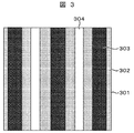
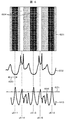
- FIG. 4 shows a secondary electron profile 401 created from the electron microscope image 301.
- the secondary electron profile is created by projecting all or part of the electron microscope image 301 in the x direction.
- the profile corresponding to the upper layer pattern 204 (upper layer pattern profile 402) is high, and the profile corresponding to the lower layer pattern 203 (lower layer pattern profile 403) is low.
- peaks due to the edge effect of secondary electrons are seen on the left and right of the upper layer pattern profile 402. This is because when the edge part where the surfaces with different angles are in contact with each other is scanned with an electron beam, secondary electrons are more likely to be emitted at the edge part than the flat surface. The amount also increases.
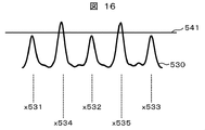
- FIG. 16 illustrates a method of discriminating an upper layer pattern and a lower layer pattern using another symmetry profile 530 obtained from the secondary electron profile 401 described above.
- the reason for the difference from the symmetry profile 501 is due to the difference in the size of the arbitrary region 520.
- a peak having an arbitrary threshold value 521 or higher can be determined as an upper layer pattern, and a peak below the threshold value 521 can be determined as a lower layer pattern.
- the amount of deviation can be obtained by equation (1) using the values x531 to x535 as in FIG.
- both the center of gravity of the upper layer pattern and the center of gravity of the lower layer pattern are obtained using the symmetry profile.
- the center-of-gravity position of the upper layer pattern may be the center of the peaks of the two edges of the upper layer pattern.
- the signal amount is insufficient, it is better to detect the centroid position based on the correlation value. From the viewpoint of reducing the number of processing steps, it is possible to obtain both centroids only by calculating the correlation value. desirable.
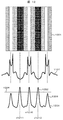
- FIG. 6 shows an electron microscope image 601 and a created secondary electron profile 602 when the upper layer pattern shift is large, and a symmetry profile 603 created by the same procedure as in FIG. Since the upper layer pattern 604 is shifted to the left, it is difficult to separate the upper layer and lower layer pattern signals in the secondary electron profile 602. Even in this case, a portion having a signal amount equal to or greater than an arbitrary threshold value 621 can be recognized as a pattern from the symmetry profile 603 as described above.
- the shift amount can be calculated from the recognized upper layer and lower layer pattern positions (x611 to x615) using equation (1).
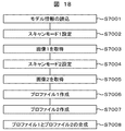
- Profile 1 is obtained by projecting image 1 (S7006).
- profile 2 is obtained from image 2 (S7007).
- Examples of profile 1 and profile 2 are shown in secondary electron profile 701 and secondary electron profile 702 in FIG.
- the signal intensity of the right edge 711 is higher than that of the left edge 710.
- the signal strength of the right edge 721 is lower than that of the left edge 720.
- a composite profile 703 is created from profile 1 and profile 2. The synthesis can be simply averaged or weighted by signal strength.
- the left and right edges of the composite profile 703 have substantially the same height (left edge 730, right edge 731).
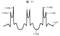
- FIG. 11 shows a secondary electron profile 1101 obtained from the electron microscope image 1001. Even in the secondary electron profile, the outer edge luminance is lower (outer edge luminance 1102 and 1105) and the inner edge luminance is higher (inner edge luminance 1103 and 1106) in the upper and lower outer layer patterns. It has become.
- the respective values are input from the upper layer pattern number input box 2015 and the lower layer pattern number input box 2014.
- the number of patterns is used to determine an arbitrary threshold value 521 or threshold value 541, an arbitrary threshold value 621, and an arbitrary threshold value 1204 in the upper layer pattern and lower layer pattern position detection (S5005).
- an arbitrary threshold value 621 is raised and lowered so as to match the number of upper layer patterns and lower layer patterns inputted.
- the operator can also input respective values from the upper pattern width input box 2017 and the lower pattern width input box 2016. These values are used as an arbitrary area 520 and an arbitrary area 620 used when creating a symmetry profile.
Landscapes
- Physics & Mathematics (AREA)
- General Physics & Mathematics (AREA)
- Chemical & Material Sciences (AREA)
- Analytical Chemistry (AREA)
- Electromagnetism (AREA)
- Health & Medical Sciences (AREA)
- Life Sciences & Earth Sciences (AREA)
- Biochemistry (AREA)
- General Health & Medical Sciences (AREA)
- Immunology (AREA)
- Pathology (AREA)
- Length-Measuring Devices Using Wave Or Particle Radiation (AREA)
Abstract
Description
ずれ量=(x511+x512+x513)
/3-(x514+x515)/2 …式(1)
ずれ量=x821-x820 …式(2)
ずれ量=x1210-(x1211+x1212)/2 …式(3)
102 引出電極
103 一次電子線
104 第一コンデンサレンズ
105 絞り
106 第二コンデンサレンズ
107 二次電子検出器
108 アライメントコイル
109 偏向コイル
110 対物レンズ
111、201 ウェーハ
112 ステージ
113 試料室
114 二次電子
115 高電圧制御装置
116 第一コンデンサレンズ制御部
117 第二コンデンサレンズ制御部
118 二次電子信号増幅器
119 アライメント制御部
120、122 偏向信号制御部
121 対物レンズ制御部
123 画像処理プロセッサ
124 二次電子像表示装置
125 全体制御部
126 電子光学系制御装置
127 ステージ制御装置
128 ユーザーインターフェース
202、203 下層パターン
204 上層パターン
205 反射防止膜
301、1001 電子顕微鏡像
302 基盤であるウェーハ表面からの二次電子信号部分
303 輝度が低く黒く見える部分
304 輝度が高く白く見える部分
401 二次電子プロファイル
402 上層パターンプロファイル
403 下層パターンプロファイル
501、1201 対称性プロファイル
x511、x512、x513、x514、x515 重心位置
x531、x532、x533、x1211、x1212 下層の各パターンの重心位置x534、x535 上層の各パターンの重心位置
520 任意領域
521、522、621、810、811、1204 任意のしきい値
530 別の対称性プロファイル
601 ずれが大きい場合の電子顕微鏡像
602、701、702、1101 二次電子プロファイル
603 ずれが大きい場合の対称性プロファイル
703 合成プロファイル
710、720、730 左エッジ
711、721、731 右エッジ
802 反転プロファイル
x820、x1210 上層パターンの重心位置
x821 下層パターンの重心位置
903 内側のパターン
904 外側のパターン
1003 非対称なパターンの傾斜に相当する電子顕微鏡像上の領域
1102、1105 外側のエッジ輝度
1103、1106 内側のエッジ輝度
1104 内側パターンの右エッジの二次電子プロファイル上の輝度
2010 オーバーレイパターン計測のパラメータを設定するための画面
2011 オフセット入力ボックス
2012 パターン情報チェックボックス
2014 下層のパターン数入力ボックス
2015 上層のパターン数入力ボックス
2016 下層のパターン幅入力ボックス
2017 上層のパターン幅入力ボックス
2020 スキャンモード
2021 対称選択チェックボックス
2022 非対称選択チェックボックス
Claims (10)
- 荷電粒子線装置によって得られた信号波形に基づいて、試料上に形成されたパターンの測定を行う演算処理装置を備えたオーバーレイ誤差測定装置において、
前記演算処理装置は、前記信号波形の部分的な抽出に基づいて得られる部分波形を用いて、前記信号波形との相関を求め、当該相関を示す相関プロファイルを形成し、当該相関プロファイルを用いて異なるレイヤに属するパターン間の寸法を測定することを特徴とするオーバーレイ誤差測定装置。 - 請求項1において、
前記演算処理装置は、前記部分的に抽出された信号波形を反転して前記部分波形を生成することを特徴とするオーバーレイ誤差測定装置。 - 請求項1において、
前記演算処理装置は、前記異なるレイヤに属するパターンの重心位置間の寸法を測定することを特徴とするオーバーレイ誤差測定装置。 - 請求項3において、
前記演算処理装置は、上層のレイヤと下層のレイヤとの間の重心位置を測定すると共に、少なくとも当該下層のレイヤの重心位置を、前記相関プロファイルを用いて特定することを特徴とするオーバーレイ誤差測定装置。 - 荷電粒子線装置によって得られた信号波形に基づいて、試料上に形成されたパターンの測定をコンピューターに実行させるコンピュータープログラムにおいて、
当該プログラムは前記コンピューターに、前記信号波形の部分的な抽出に基づいて得られる部分波形と、前記信号波形との相関を求めさせ、当該相関を示す相関プロファイルを形成させ、当該相関プロファイルを用いて異なるレイヤに属するパターン間の寸法を測定させることを特徴とするコンピュータープログラム。 - 荷電粒子線装置によって得られた信号波形に基づいて、試料上に形成されたパターンの測定を行う演算処理装置を備えたオーバーレイ誤差測定装置において、
前記演算処理装置は、前記信号波形について、所定値以上の輝度を持つ部分と、当該所定値未満の輝度を持つ部分とを識別し、当該所定値以上の輝度を持つ部分から第1の測定基準を抽出すると共に、当該所定値未満の輝度を持つ部分から第2の測定基準を抽出し、当該第1の測定基準と第2の測定基準との間の寸法を測定することを特徴とするオーバーレイ誤差測定装置。 - 請求項6において、
前記演算処理装置は、前記所定値未満の輝度を持つ部分から、パターンの重心位置を抽出し、当該重心位置を前記第2の測定基準とすることを特徴とするオーバーレイ誤差測定装置。 - 請求項6において、
前記演算処理装置は、前記所定値未満の輝度を持つ部分の一部を抽出し、当該抽出された信号波形を反転して、部分波形を生成することを特徴とするオーバーレイ誤差測定装置。 - 請求項8において、
前記演算処理装置は、前記部分波形を用いて、前記信号波形をサーチすることによって、前記第2の測定基準、或いは前記第1の測定基準と第2の測定基準の双方を抽出することを特徴とするオーバーレイ誤差測定装置。 - 荷電粒子線装置によって得られた信号波形に基づいて、試料上に形成されたパターンの測定をコンピューターに実行させるコンピュータープログラムにおいて、
当該プログラムは前記コンピューターに、前記信号波形について、所定値以上の輝度を持つ部分と、当該所定値未満の輝度を持つ部分とを識別させ、当該所定値以上の輝度を持つ部分から第1の測定基準を抽出させると共に、当該所定値未満の輝度を持つ部分から第2の測定基準を抽出させ、当該第1の測定基準と第2の測定基準との間の寸法を測定させることを特徴とするコンピュータープログラム。
Priority Applications (2)
| Application Number | Priority Date | Filing Date | Title |
|---|---|---|---|
| US14/413,198 US10545017B2 (en) | 2012-07-06 | 2013-06-05 | Overlay error measuring device and computer program for causing computer to measure pattern |
| KR1020147031970A KR101730918B1 (ko) | 2012-07-06 | 2013-06-05 | 오버레이 오차 측정 장치, 및 패턴 측정을 컴퓨터에 실행시키는 컴퓨터 프로그램 |
Applications Claiming Priority (2)
| Application Number | Priority Date | Filing Date | Title |
|---|---|---|---|
| JP2012-152008 | 2012-07-06 | ||
| JP2012152008A JP6002480B2 (ja) | 2012-07-06 | 2012-07-06 | オーバーレイ誤差測定装置、及びパターン測定をコンピューターに実行させるコンピュータープログラム |
Publications (1)
| Publication Number | Publication Date |
|---|---|
| WO2014007017A1 true WO2014007017A1 (ja) | 2014-01-09 |
Family
ID=49881777
Family Applications (1)
| Application Number | Title | Priority Date | Filing Date |
|---|---|---|---|
| PCT/JP2013/065526 Ceased WO2014007017A1 (ja) | 2012-07-06 | 2013-06-05 | オーバーレイ誤差測定装置、及びパターン測定をコンピューターに実行させるコンピュータープログラム |
Country Status (5)
| Country | Link |
|---|---|
| US (1) | US10545017B2 (ja) |
| JP (1) | JP6002480B2 (ja) |
| KR (1) | KR101730918B1 (ja) |
| TW (1) | TWI493154B (ja) |
| WO (1) | WO2014007017A1 (ja) |
Cited By (1)
| Publication number | Priority date | Publication date | Assignee | Title |
|---|---|---|---|---|
| CN106096244A (zh) * | 2016-06-02 | 2016-11-09 | 西北核技术研究所 | 一种感应电压叠加器次级磁绝缘电子鞘层边界的确定方法 |
Families Citing this family (17)
| Publication number | Priority date | Publication date | Assignee | Title |
|---|---|---|---|---|
| JP6378927B2 (ja) * | 2014-04-25 | 2018-08-22 | 株式会社日立ハイテクノロジーズ | 計測システムおよび計測方法 |
| US20170146465A1 (en) * | 2014-06-19 | 2017-05-25 | Nova Measuring Instruments Ltd. | Test structure design for metrology measurements in patterned samples |
| JP6737879B2 (ja) * | 2015-10-12 | 2020-08-12 | エーエスエムエル ホールディング エヌ.ブイ. | センサを備えた装置、及びターゲット測定を実行する方法 |
| KR102143803B1 (ko) * | 2016-09-01 | 2020-08-12 | 주식회사 히타치하이테크 | 화상 해석 장치 및 하전 입자선 장치 |
| KR102737499B1 (ko) * | 2016-12-16 | 2024-12-05 | 삼성전자주식회사 | 오버레이 패턴들을 포함하는 반도체 소자 |
| KR102392338B1 (ko) * | 2017-10-13 | 2022-05-02 | 주식회사 히타치하이테크 | 패턴 계측 장치 및 패턴 계측 방법 |
| US10473460B2 (en) * | 2017-12-11 | 2019-11-12 | Kla-Tencor Corporation | Overlay measurements of overlapping target structures based on symmetry of scanning electron beam signals |
| US10533848B2 (en) * | 2018-03-05 | 2020-01-14 | Kla-Tencor Corporation | Metrology and control of overlay and edge placement errors |
| US10446367B2 (en) * | 2018-03-07 | 2019-10-15 | Kla-Tencor Corporation | Scan strategies to minimize charging effects and radiation damage of charged particle beam metrology system |
| CN110349874B (zh) * | 2018-04-04 | 2021-06-04 | 中芯国际集成电路制造(上海)有限公司 | 一种套刻对准的检测方法 |
| JP7305422B2 (ja) * | 2019-05-13 | 2023-07-10 | 株式会社日立ハイテク | パターン評価システム及びパターン評価方法 |
| WO2021038649A1 (ja) * | 2019-08-23 | 2021-03-04 | 株式会社日立ハイテク | オーバーレイ計測システム及びオーバーレイ計測装置 |
| KR102880958B1 (ko) * | 2020-12-16 | 2025-11-05 | 주식회사 히타치하이테크 | 패턴 계측 장치 |
| CN114623787B (zh) * | 2022-03-10 | 2024-05-03 | 长鑫存储技术有限公司 | 用于校准套刻量测准确性的校准标记及测量方法、校准方法 |
| US20240094639A1 (en) * | 2022-09-19 | 2024-03-21 | Kla Corporation | High-resolution evaluation of optical metrology targets for process control |
| KR20240048213A (ko) * | 2022-10-06 | 2024-04-15 | 삼성전자주식회사 | 오버레이 측정 방법, 오버레이 측정 시스템 및 이를 이용한 반도체 장치의 제조 방법 |
| KR20240174381A (ko) * | 2023-06-08 | 2024-12-17 | 삼성전자주식회사 | 패턴 검사 장치 및 패턴 검사 방법 |
Citations (6)
| Publication number | Priority date | Publication date | Assignee | Title |
|---|---|---|---|---|
| JPS6197510A (ja) * | 1984-10-19 | 1986-05-16 | Hitachi Ltd | 走査型電子顕微鏡による立体形状測定装置 |
| WO2010038859A1 (ja) * | 2008-10-03 | 2010-04-08 | 株式会社 日立ハイテクノロジーズ | パターンマッチング方法、及び画像処理装置 |
| JP2011033423A (ja) * | 2009-07-31 | 2011-02-17 | Hitachi High-Technologies Corp | パターン形状選択方法、及びパターン測定装置 |
| JP2011142321A (ja) * | 2009-12-29 | 2011-07-21 | Hitachi Ltd | パターン位置およびオーバレイ測定方法および装置 |
| JP2012177961A (ja) * | 2011-02-25 | 2012-09-13 | Hitachi High-Technologies Corp | パターンマッチング装置、及びコンピュータープログラム |
| JP2012244142A (ja) * | 2011-05-19 | 2012-12-10 | Applied Materials Israel Ltd | 高電子エネルギベースのオーバーレイ誤差測定方法及びシステム |
Family Cites Families (17)
| Publication number | Priority date | Publication date | Assignee | Title |
|---|---|---|---|---|
| JP3326931B2 (ja) * | 1993-11-29 | 2002-09-24 | 株式会社ニコン | 重ね合わせ精度測定方法および測定装置 |
| WO1996010148A1 (en) * | 1994-09-27 | 1996-04-04 | Minnesota Mining And Manufacturing Company | Luminance control film |
| US6407396B1 (en) * | 1999-06-24 | 2002-06-18 | International Business Machines Corporation | Wafer metrology structure |
| US20020041377A1 (en) * | 2000-04-25 | 2002-04-11 | Nikon Corporation | Aerial image measurement method and unit, optical properties measurement method and unit, adjustment method of projection optical system, exposure method and apparatus, making method of exposure apparatus, and device manufacturing method |
| JP2003022954A (ja) | 2001-07-09 | 2003-01-24 | Nikon Corp | 重ね合わせ誤差測定装置 |
| CN100479097C (zh) * | 2004-08-19 | 2009-04-15 | 株式会社尼康 | 对准信息显示方法及其程序、对准方法、曝光方法、组件制造方法、显示系统、显示装置、程序及测定/检查装置 |
| JP2006234588A (ja) * | 2005-02-25 | 2006-09-07 | Hitachi High-Technologies Corp | パターン測定方法、及びパターン測定装置 |
| JP4635711B2 (ja) * | 2005-05-13 | 2011-02-23 | 株式会社ニコン | 重ね合わせ測定装置 |
| KR100598988B1 (ko) | 2005-05-18 | 2006-07-12 | 주식회사 하이닉스반도체 | 오버레이 버니어 및 이를 이용한 반도체소자의 제조방법 |
| JP4585926B2 (ja) * | 2005-06-17 | 2010-11-24 | 株式会社日立ハイテクノロジーズ | パターンレイヤーデータ生成装置、それを用いたパターンレイヤーデータ生成システム、半導体パターン表示装置、パターンレイヤーデータ生成方法、及びコンピュータプログラム |
| US7923703B2 (en) * | 2006-02-17 | 2011-04-12 | Hitachi High-Technologies Corporation | Sample dimension inspecting/measuring method and sample dimension inspecting/measuring apparatus |
| JP4887062B2 (ja) | 2006-03-14 | 2012-02-29 | 株式会社日立ハイテクノロジーズ | 試料寸法測定方法、及び試料寸法測定装置 |
| US7630087B2 (en) * | 2006-11-22 | 2009-12-08 | Asml Netherlands B.V. | Inspection method and apparatus, lithographic apparatus, lithographic processing cell and device manufacturing method |
| JP5530601B2 (ja) * | 2008-03-31 | 2014-06-25 | 株式会社日立ハイテクノロジーズ | 走査型電子顕微鏡を用いた回路パターンの寸法計測装置およびその方法 |
| NL1036734A1 (nl) * | 2008-04-09 | 2009-10-12 | Asml Netherlands Bv | A method of assessing a model, an inspection apparatus and a lithographic apparatus. |
| JP5500858B2 (ja) * | 2009-04-14 | 2014-05-21 | 株式会社日立ハイテクノロジーズ | パターン測定装置 |
| KR101492205B1 (ko) * | 2010-11-12 | 2015-02-10 | 에이에스엠엘 네델란즈 비.브이. | 메트롤로지 방법 및 장치, 리소그래피 시스템, 및 디바이스 제조 방법 |
-
2012
- 2012-07-06 JP JP2012152008A patent/JP6002480B2/ja active Active
-
2013
- 2013-05-30 TW TW102119149A patent/TWI493154B/zh active
- 2013-06-05 US US14/413,198 patent/US10545017B2/en active Active
- 2013-06-05 WO PCT/JP2013/065526 patent/WO2014007017A1/ja not_active Ceased
- 2013-06-05 KR KR1020147031970A patent/KR101730918B1/ko active Active
Patent Citations (6)
| Publication number | Priority date | Publication date | Assignee | Title |
|---|---|---|---|---|
| JPS6197510A (ja) * | 1984-10-19 | 1986-05-16 | Hitachi Ltd | 走査型電子顕微鏡による立体形状測定装置 |
| WO2010038859A1 (ja) * | 2008-10-03 | 2010-04-08 | 株式会社 日立ハイテクノロジーズ | パターンマッチング方法、及び画像処理装置 |
| JP2011033423A (ja) * | 2009-07-31 | 2011-02-17 | Hitachi High-Technologies Corp | パターン形状選択方法、及びパターン測定装置 |
| JP2011142321A (ja) * | 2009-12-29 | 2011-07-21 | Hitachi Ltd | パターン位置およびオーバレイ測定方法および装置 |
| JP2012177961A (ja) * | 2011-02-25 | 2012-09-13 | Hitachi High-Technologies Corp | パターンマッチング装置、及びコンピュータープログラム |
| JP2012244142A (ja) * | 2011-05-19 | 2012-12-10 | Applied Materials Israel Ltd | 高電子エネルギベースのオーバーレイ誤差測定方法及びシステム |
Cited By (2)
| Publication number | Priority date | Publication date | Assignee | Title |
|---|---|---|---|---|
| CN106096244A (zh) * | 2016-06-02 | 2016-11-09 | 西北核技术研究所 | 一种感应电压叠加器次级磁绝缘电子鞘层边界的确定方法 |
| CN106096244B (zh) * | 2016-06-02 | 2018-10-26 | 西北核技术研究所 | 一种感应电压叠加器次级磁绝缘电子鞘层边界的确定方法 |
Also Published As
| Publication number | Publication date |
|---|---|
| KR20140146658A (ko) | 2014-12-26 |
| US20150285627A1 (en) | 2015-10-08 |
| JP6002480B2 (ja) | 2016-10-05 |
| KR101730918B1 (ko) | 2017-04-27 |
| JP2014016174A (ja) | 2014-01-30 |
| TWI493154B (zh) | 2015-07-21 |
| US10545017B2 (en) | 2020-01-28 |
| TW201414986A (zh) | 2014-04-16 |
Similar Documents
| Publication | Publication Date | Title |
|---|---|---|
| JP6002480B2 (ja) | オーバーレイ誤差測定装置、及びパターン測定をコンピューターに実行させるコンピュータープログラム | |
| KR101828124B1 (ko) | 패턴 평가 방법 및 패턴 평가 장치 | |
| JP5986817B2 (ja) | オーバーレイ誤差測定装置、及びコンピュータープログラム | |
| JP5639797B2 (ja) | パターンマッチング方法,画像処理装置、及びコンピュータプログラム | |
| JP6043735B2 (ja) | 画像評価装置及びパターン形状評価装置 | |
| US8295584B2 (en) | Pattern measurement methods and pattern measurement equipment | |
| JP5500858B2 (ja) | パターン測定装置 | |
| US8330104B2 (en) | Pattern measurement apparatus and pattern measurement method | |
| US20090232385A1 (en) | Pattern measuring method and pattern measuring device | |
| JP5164598B2 (ja) | レビュー方法、およびレビュー装置 | |
| JP6061496B2 (ja) | パターン計測装置、パターン計測方法及びパターン計測プログラム | |
| KR20170093931A (ko) | 패턴 측정 장치 및 결함 검사 장치 | |
| JP2015210140A (ja) | 計測システムおよび計測方法 | |
| US20130150998A1 (en) | Managing apparatus of semiconductor manufacturing apparatus and computer program | |
| US10190875B2 (en) | Pattern measurement condition setting device and pattern measuring device | |
| JP6043528B2 (ja) | パターン測定装置 | |
| JP5953117B2 (ja) | パターン評価装置、及びコンピュータープログラム | |
| JP6207893B2 (ja) | 試料観察装置用のテンプレート作成装置 | |
| US8878129B1 (en) | Pattern measurement apparatus and pattern measurement method | |
| JP2017020981A (ja) | パターン測定装置、及びコンピュータープログラム |
Legal Events
| Date | Code | Title | Description |
|---|---|---|---|
| 121 | Ep: the epo has been informed by wipo that ep was designated in this application |
Ref document number: 13813433 Country of ref document: EP Kind code of ref document: A1 |
|
| ENP | Entry into the national phase |
Ref document number: 20147031970 Country of ref document: KR Kind code of ref document: A |
|
| WWE | Wipo information: entry into national phase |
Ref document number: 14413198 Country of ref document: US |
|
| NENP | Non-entry into the national phase |
Ref country code: DE |
|
| 122 | Ep: pct application non-entry in european phase |
Ref document number: 13813433 Country of ref document: EP Kind code of ref document: A1 |