WO2014006882A1 - 固体撮像装置およびその駆動方法、並びに電子情報機器 - Google Patents
固体撮像装置およびその駆動方法、並びに電子情報機器 Download PDFInfo
- Publication number
- WO2014006882A1 WO2014006882A1 PCT/JP2013/004097 JP2013004097W WO2014006882A1 WO 2014006882 A1 WO2014006882 A1 WO 2014006882A1 JP 2013004097 W JP2013004097 W JP 2013004097W WO 2014006882 A1 WO2014006882 A1 WO 2014006882A1
- Authority
- WO
- WIPO (PCT)
- Prior art keywords
- unit
- addition
- gate
- vertical transfer
- pixel
- Prior art date
- Legal status (The legal status is an assumption and is not a legal conclusion. Google has not performed a legal analysis and makes no representation as to the accuracy of the status listed.)
- Ceased
Links
Images





Classifications
-
- H—ELECTRICITY
- H10—SEMICONDUCTOR DEVICES; ELECTRIC SOLID-STATE DEVICES NOT OTHERWISE PROVIDED FOR
- H10F—INORGANIC SEMICONDUCTOR DEVICES SENSITIVE TO INFRARED RADIATION, LIGHT, ELECTROMAGNETIC RADIATION OF SHORTER WAVELENGTH OR CORPUSCULAR RADIATION
- H10F39/00—Integrated devices, or assemblies of multiple devices, comprising at least one element covered by group H10F30/00, e.g. radiation detectors comprising photodiode arrays
- H10F39/10—Integrated devices
- H10F39/12—Image sensors
- H10F39/15—Charge-coupled device [CCD] image sensors
- H10F39/153—Two-dimensional or three-dimensional array CCD image sensors
-
- H—ELECTRICITY
- H04—ELECTRIC COMMUNICATION TECHNIQUE
- H04N—PICTORIAL COMMUNICATION, e.g. TELEVISION
- H04N25/00—Circuitry of solid-state image sensors [SSIS]; Control thereof
- H04N25/40—Extracting pixel data from image sensors by controlling scanning circuits, e.g. by modifying the number of pixels sampled or to be sampled
- H04N25/44—Extracting pixel data from image sensors by controlling scanning circuits, e.g. by modifying the number of pixels sampled or to be sampled by partially reading an SSIS array
- H04N25/447—Extracting pixel data from image sensors by controlling scanning circuits, e.g. by modifying the number of pixels sampled or to be sampled by partially reading an SSIS array by preserving the colour pattern with or without loss of information
-
- H—ELECTRICITY
- H04—ELECTRIC COMMUNICATION TECHNIQUE
- H04N—PICTORIAL COMMUNICATION, e.g. TELEVISION
- H04N23/00—Cameras or camera modules comprising electronic image sensors; Control thereof
- H04N23/10—Cameras or camera modules comprising electronic image sensors; Control thereof for generating image signals from different wavelengths
-
- H—ELECTRICITY
- H04—ELECTRIC COMMUNICATION TECHNIQUE
- H04N—PICTORIAL COMMUNICATION, e.g. TELEVISION
- H04N25/00—Circuitry of solid-state image sensors [SSIS]; Control thereof
- H04N25/40—Extracting pixel data from image sensors by controlling scanning circuits, e.g. by modifying the number of pixels sampled or to be sampled
- H04N25/42—Extracting pixel data from image sensors by controlling scanning circuits, e.g. by modifying the number of pixels sampled or to be sampled by switching between different modes of operation using different resolutions or aspect ratios, e.g. switching between interlaced and non-interlaced mode
-
- H—ELECTRICITY
- H04—ELECTRIC COMMUNICATION TECHNIQUE
- H04N—PICTORIAL COMMUNICATION, e.g. TELEVISION
- H04N25/00—Circuitry of solid-state image sensors [SSIS]; Control thereof
- H04N25/40—Extracting pixel data from image sensors by controlling scanning circuits, e.g. by modifying the number of pixels sampled or to be sampled
- H04N25/46—Extracting pixel data from image sensors by controlling scanning circuits, e.g. by modifying the number of pixels sampled or to be sampled by combining or binning pixels
-
- H—ELECTRICITY
- H04—ELECTRIC COMMUNICATION TECHNIQUE
- H04N—PICTORIAL COMMUNICATION, e.g. TELEVISION
- H04N25/00—Circuitry of solid-state image sensors [SSIS]; Control thereof
- H04N25/70—SSIS architectures; Circuits associated therewith
- H04N25/71—Charge-coupled device [CCD] sensors; Charge-transfer registers specially adapted for CCD sensors
- H04N25/715—Charge-coupled device [CCD] sensors; Charge-transfer registers specially adapted for CCD sensors using frame interline transfer [FIT]
-
- H—ELECTRICITY
- H04—ELECTRIC COMMUNICATION TECHNIQUE
- H04N—PICTORIAL COMMUNICATION, e.g. TELEVISION
- H04N25/00—Circuitry of solid-state image sensors [SSIS]; Control thereof
- H04N25/70—SSIS architectures; Circuits associated therewith
- H04N25/71—Charge-coupled device [CCD] sensors; Charge-transfer registers specially adapted for CCD sensors
- H04N25/73—Charge-coupled device [CCD] sensors; Charge-transfer registers specially adapted for CCD sensors using interline transfer [IT]
Definitions
- the present invention relates to a solid-state imaging device, a driving method thereof, and an electronic information device.
- a solid-state imaging device capable of capturing a still image and a moving image
- a signal charge is transferred from a vertical transfer unit to a horizontal transfer unit.
- the present invention relates to a device having an operation mode for adding signal charges, a method for driving such a solid-state imaging device, and an electronic information device including such a solid-state imaging device.
- solid-state imaging devices include CMOS image sensors and CCD image sensors, and these image sensors are used as imaging devices such as digital still cameras and video cameras.
- Each image sensor uses a photodiode as an element for photoelectrically converting light from a subject.
- these image sensors output signal charges obtained by the photodiode to an image corresponding to each pixel outside the image sensor.
- the extraction method is different as a signal (hereinafter referred to as a pixel signal).
- a CCD image sensor uses a vertical transfer unit (vertical CCD) and a horizontal transfer unit (horizontal CCD) to transfer signal charges to one output unit, which converts the signal charges into voltage signals and amplifies them.
- a CMOS image sensor converts a signal charge into a voltage signal for each photodiode, amplifies it, and outputs it as a pixel signal.
- CCD image sensors By the way, in recent years, digital still cameras have rapidly improved in image quality, and solid-state imaging devices having a number of pixels of 10 million pixels or more, in particular, CCD image sensors are widely used.
- an operation mode (still mode) for driving a vertical CCD and a horizontal CCD so that a still image can be obtained by independently reading out signal charges of all pixels, and a moving image is displayed on a liquid crystal monitor or the like.
- the operation mode (monitoring mode) for driving the vertical CCD and the horizontal CCD is switched so as to obtain the image signal.
- the drive frequency can be increased from the viewpoint of the limit of the drive frequency characteristics of the CCD image sensor or low power consumption.
- a CCD image sensor having a number of pixels of 1.3 million pixels or more generally attempts to improve the frame rate by the following two methods.
- the frequency of outputting pixel signals corresponding to individual pixels is reduced, thereby improving the frame rate.
- Patent Document 1 the method disclosed in Patent Document 1 is not practical because it increases the cost of the signal processing unit due to an increase in the output unit.
- the frame rate is improved by adding the signal charges from a plurality of arbitrary pixels to reduce the amount of data, that is, the number of signal charges to be transferred as pixel values.
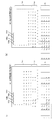
- FIG. 14 is a diagram for explaining a CCD image sensor which is a conventional solid-state imaging device.
- FIG. 14A shows a pixel row of this CCD image sensor and the arrangement of corresponding vertical transfer units, and FIG. ) Shows the flow of signal charges from the vertical transfer unit to the horizontal transfer unit.
- the CCD image sensor 5 includes a pixel unit 5a including a plurality of pixels PD arranged in a matrix, and is provided corresponding to each pixel column of the plurality of pixels.
- Vertical transfer units (VCCD units) 500a to 500d that transfer signal charges in the vertical direction, and horizontal transfers that are provided on the transfer termination side of these VCCD units 500a to 500d and transfer signal charges from each VCCD unit in the horizontal direction Part (HCCD part) 1b.
- the VCCD units 500a to 500d operate as an operation mode by adding a signal charge when the signal charge is transferred to the HCCD unit 1b (monitoring mode), and by adding the signal charge without adding the signal charge. It has a normal mode (still mode) for transferring to the HCCD unit 1b.
- the pixel unit 5a includes a pixel gate unit (transfer gate region) 5ac that performs signal charge transfer at the same timing in all the VCCD units 500a to 500d regardless of the operation mode, and a part of the VCCD unit 500a.
- 500b and the other VCCD units 500c and 500d are configured to be transferable at different transfer timings, and have an addition gate unit (addition gate region) 5as that switches between the addition mode and the normal mode according to the drive signal.
- the part 5as is located adjacent to the HCCD part 1b.
- the transfer gate region 5ac of the pixel unit 5a includes a light-shielded light-shielding region 5a2 on the HCCD unit 1b side of the VCCD units 500a to 500d and a non-light-shielded non-light-shielded region 5a1 other than the light-shielding region 5a2. Is arranged.
- the first to fourth pixel columns 50a to 50d and the corresponding first to fourth columns are shown. Only the VCCD units 500a to 500d are shown, but in an actual CCD image sensor, the pixel column and the VCCD unit include not only four columns but more columns according to the number of pixels. Each pixel is provided with a color filter, and the red pixel (R), green pixel (G), and blue pixel (B) array is a Bayer array.
- the transfer gate region 5ac of the VCCD section 500a of the first column four normal transfer gates 501 to 504 are arranged along the vertical direction for each pixel PD of the corresponding pixel column 50a.
- the addition gate region 5as of the VCCD section 500a in the first column four normal transfer gates (hereinafter also simply referred to as transfer gates) 501 to 504 and two transfer gates for addition (hereinafter referred to as addition gates). 505 and 506 are arranged along the vertical transfer direction.
- the arrangement of transfer gates and addition gates in the VCCD section 500b in the second column is exactly the same as that in the VCCD section 500a in the first column.
- the pixel gate portion 5ac of the VCCD portion 500c in the third column four transfer gates 501 to 504 are arranged along the vertical direction for each pixel PD in the corresponding pixel column 50c.
- the addition gate unit 5as of the VCCD unit 500c in the column two transfer gates 501 and 502 and two transfer gates for addition (hereinafter also referred to as addition gates) 503a and 504a are arranged along the vertical direction. Are arranged.
- the transfer gates 503a and 504a for addition are twice as long in the transfer direction as the normal transfer gates 503 and 504.
- vertical transfer pulses ⁇ V1 to ⁇ V4 are applied to the transfer gates 501 to 504 as drive signals
- vertical transfer pulses ⁇ V3 and ⁇ V4 are applied to the addition gates 503a and 504a as drive signals
- the addition gate 505 and In 506 vertical transfer pulses ⁇ Vs5 and ⁇ Vs6 independent of the vertical transfer pulses ⁇ V1 to ⁇ V4 are applied.
- the third and fourth VCCD units 500c and 500d As indicated by solid arrows in FIG. 14B, the signal charges of each pixel are sequentially transferred to the HCCD unit 1b, and the HCCD unit 1b driven by a two-phase horizontal transfer pulse (not shown) is horizontally Will be transferred in the direction.
- the signal charges of the respective pixels are sequentially transferred to the HCCD unit 1b as shown by the dotted arrows in FIG.
- vertical transfer pulses ⁇ Vs5 and ⁇ Vs6 independent from the vertical transfer pulses ⁇ V1 to ⁇ V4 are applied to the addition gates 505 and 506 adjacent to the HCCD unit 1b, so that the third and fourth VCCD units
- the signal charges transferred from 500c and 500d to the HCCD unit 1b are transferred to positions corresponding to the first and second VCCD units 500a and 500b until the first and second VCCD units 500a.
- the signal charges are prevented from being transferred from 500b to HCCD unit 1b.
- the signal charges are transferred from the VCCD units 500a to 500d to the HCCD unit 1b
- the signal charges from the first and second VCCD units 500a and 500b are transferred to the third and fourth VCCD units. It can be added to the signal charges from 500c and 500d.
- the charge transfer packets (hereinafter abbreviated as transfer packets) of the VCCD units 500a to 500d are shown in FIG. Assume that the signal charges (R), (G), and (B) read from the corresponding pixel columns 50a to 50d are accumulated as shown in FIG.
- the signal charges from the VCCD units 500c and 500d in the third and fourth columns pass through the HCCD unit 1b, and the VCCDs in the first and second columns.
- the transfer barrier immediately below the addition gate 506 is eliminated, so that the first and second as shown in FIG.
- Signal charges (R) and (G) are transferred from VCCD units 500a and 500b to HCCD unit 1b, and signal charges (R) and (G) from VCCD units 500c and 500d in the third and fourth columns are transferred. Is added.
- the signal charges of the VCCD units 500a to 500d are transferred in the vertical direction by one cycle, and further added in the HCCD unit 1b as shown in FIG. 15 (f).
- the signal charges (R) and (G) are transferred in the horizontal direction.
- the pixel unit 5a includes the VCCD units 500c and 500d having a small total number of transfer gates and addition gates (the number of gates) and a large total number of transfer gates and addition gates (the number of gates).
- the VCCD units 500a and 500b coexist, and the signal charge of the VCCD unit with a small number of gates is read to the HCCD unit first, and the signal charge previously read to the HCCD unit is transferred forward (left side) in the HCCD unit. After that, the signal charges are added by reading the signal charges from the VCCD unit having a large number of gates to the HCCD unit.
- the length in the transfer direction of the transfer gates for addition (addition gates) included in the addition gate unit 5as is included in the plurality of VCCD units corresponding to the respective pixel columns constituting the pixel unit.
- a plurality of VCCD portions corresponding to each pixel column constituting the pixel portion include a mixture of a large number and a small number of gates. ing.
- the charge transfer time becomes long, and waveform rounding occurs due to the large gate additional capacity.
- Charge transfer is performed under a very disadvantageous condition for charge transfer. That is, the above-described conventional solid-state imaging device is disadvantageous in improving the frame rate because the gate length of the addition gate included in the addition gate unit is longer than the gate length of the normal transfer gate included in the pixel gate unit. There is a problem in that image quality deterioration due to transfer degradation also occurs.
- the gate length of the transfer gate for addition included in the addition gate portion is shorter than the gate length of the normal transfer gate included in the pixel gate portion, in the transfer gate having a short gate length, the portion facing the transfer channel Since the area of the transfer packet formed by the transfer gate is reduced, the amount of handled signals, that is, the amount of signal charges that can be transferred is reduced. That is, a solid-state imaging device having a gate with a short gate length as an addition gate is disadvantageous for improving the dynamic range, and there is a problem in that the image quality at high output is reduced.
- the present invention has been made in order to solve the above-described problem, and transfers signal charges from a vertical transfer unit to a horizontal transfer unit in a vertical transfer unit corresponding to a specific pixel column and another pixel column.
- it is possible to perform independent transfer to and from the vertical transfer unit corresponding to the signal transfer rate, and avoid the restriction on the signal charge transfer speed and the amount of signal charges handled by the configuration that enables the transfer of the independent signal charges.
- Another object of the present invention is to obtain a solid-state imaging device capable of further increasing the vertical transfer speed, a driving method thereof, and an electronic information device including such a solid-state imaging device.
- a solid-state imaging device is a solid-state imaging device that has a plurality of pixels arranged in a matrix and outputs a signal charge obtained by the pixels as a pixel signal, the pixel array of the plurality of pixels
- a plurality of vertical transfer units that transfer signal charges from the pixels in the corresponding pixel column in the vertical direction, and are provided across the plurality of vertical transfer units on the transfer termination side of the plurality of vertical transfer units.
- a horizontal transfer unit that horizontally transfers the signal charges transferred from the plurality of vertical transfer units, and each of the plurality of vertical transfer units is transferred from the vertical transfer unit to the horizontal transfer unit in the addition mode.
- An addition gate unit that adds the signal charges of two or more pixels when transferring the signal charge, and the vertical length of the addition gate constituting the addition gate unit is common to the plurality of vertical transfer units There are two or more gates on the summing gate. Line is disposed so as to face the said summing gate, the objects can be achieved.
- the addition gate is connected to any one of the two or more gate wirings disposed thereon via a contact hole.
- the addition gate unit transfers the signal charge from the plurality of vertical transfer units to the horizontal transfer unit without performing addition of the signal charge in the normal mode.
- the mode and the addition mode are preferably configured to be switched by a drive signal applied to the addition gate.
- the vertical transfer unit includes a pixel gate unit that transfers the signal charge to the addition gate unit in addition to the addition gate unit, and the addition gate includes the pixel gate. It is preferably driven by a drive signal that is independent of the transfer gate constituting the part.
- the arrangement of the color filters provided in the plurality of pixels includes a first pixel column in which green pixels and red pixels are alternately arranged in the vertical direction, and a blue pixel. And the second pixel column in which the green pixels are alternately arranged along the vertical direction are arranged in an alternating manner in the horizontal direction so that the green pixels are not adjacent to each other.
- the first and second groups are divided into a first vertical transfer unit corresponding to the first pixel column and a second pixel column adjacent to the first pixel column. And a pair of adjacent first vertical transfer units and second vertical transfer units belonging to the first group, and a pair of adjacent second transfer units belonging to the second group.
- 1 vertical transfer part and 2nd vertical transfer part are horizontal It is preferably disposed alternately.
- the addition gate unit transmits the signal charge from the first vertical transfer unit of the first group to the first vertical transfer unit of the first group in the addition mode.
- the signal charge from the first vertical transfer unit of the adjacent second group is added, and the signal charge from the second vertical transfer unit of the first group is adjacent to the second vertical transfer unit of the first group. It is preferable to add the signal charge from the second vertical transfer unit of the second group.
- the vertical transfer unit includes a pixel gate unit that transfers the signal charge to the addition gate unit in addition to the addition gate unit.
- the pixel gate unit is driven by a four-phase drive signal that is independent of the four-phase drive signal that drives the addition gate unit, and the addition gate unit of the vertical transfer unit of the first group
- the driving signals for the first phase and the third phase for driving the driving signal are independent of the driving signals for the first phase and the third phase for driving the addition gates of the vertical transfer units of the second group.
- the second-phase and fourth-phase drive signals for driving the addition gates of the vertical transfer units of the first group are second signals for driving the addition gates of the vertical transfer units of the second group, respectively. Shared with the phase and fourth phase drive signals It is preferably a drive signal.
- the vertical transfer unit includes a pixel gate unit that transfers the signal charge to the addition gate unit in addition to the addition gate unit, and the addition gate unit has a three-phase structure.
- the pixel gate unit is driven by a four-phase drive signal that is independent of the three-phase drive signal that drives the addition gate unit, and the addition gate unit of the vertical transfer unit of the first group is
- the three-phase driving signal to be driven is preferably a driving signal independent of the three-phase driving signal for driving the addition gate unit of the vertical transfer unit of the second group.
- the vertical transfer unit is located between the pixel gate unit and the addition gate unit, and transfers two signal charges from the pixel gate unit to the addition gate unit
- the first to fourth transfer gates are repeatedly arranged for each pixel along the vertical direction.
- the first to third addition gates are arranged repeatedly twice along the vertical direction.
- the addition gate unit transfers signal charges from the first and second vertical transfer units of the second group to the horizontal transfer unit, and then to the horizontal transfer unit.
- the signal charges from the first and second vertical transfer units of the second group are moved to a portion facing the first and second vertical transfer units of the first group, and the first group Transfer the signal charge from the first and second vertical transfer units of the second group to the horizontal transfer unit so as to be mixed with the signal charge from the first and second vertical transfer units of the second group.
- the solid-state imaging device driving method is a method for driving the above-described solid-state imaging device according to the present invention, wherein the signal charges from the plurality of vertical transfer units are added and transferred to the horizontal transfer unit.
- the addition mode and the normal mode in which the signal charges from the plurality of vertical transfer units are transferred to the horizontal transfer unit as they are without being added are switched by a drive signal applied to the addition gate. The objective is achieved.
- An electronic information device is an electronic information device including an imaging unit that captures an image of a subject, and the imaging unit is the above-described solid-state imaging device according to the present invention. Is done.
- a solid-state imaging device having a plurality of pixels arranged in a matrix, a plurality of vertical transfer units provided for each pixel column and a horizontal transfer provided on the transfer end side of these vertical transfer units
- the vertical transfer unit has an addition gate unit for adding signal charges when transferring the signal charge from the vertical transfer unit to the horizontal transfer unit in the addition mode. Since the vertical lengths (gate lengths) of the addition gates constituting the same are shared by a plurality of vertical transfer units, the vertical lengths of the addition gates constituting the addition gate units of some of the vertical transfer units are different depending on the gate length of the addition gates. It is possible to avoid a restriction on the amount of signal charge handled by the transfer unit or the transfer speed.
- the addition gate portion two or more gate wirings are arranged on the addition gate so as to face the addition gate. Therefore, the gate wiring connected to the addition gate is selected from among the two or more gate wirings in the wiring process. You can choose.
- the operation of the addition gate unit in the normal mode or the addition mode is given priority to the magnitude of the handled signal charge by selecting the gate wiring connected to the addition gate, that is, by changing the timing of the drive signal applied to the addition gate. It is possible to select whether the operation is to be performed or to prioritize the transfer speed, and it is possible to provide a solid-state imaging device that has high performance required according to the application and has high usage efficiency.
- a camera system equipped with such a solid-state imaging device a camera system capable of obtaining a simple high frame rate image or a high dynamic range image used for a viewfinder or the like can be realized.
- switching between the amount of the handling signal charge and the transfer speed can be performed according to which of the two or more gate wirings arranged on the addition gate of the addition gate unit is connected, An appropriate switching according to the use as a solid-state imaging device can be realized at a low cost with a simple configuration.
- the addition gate unit and the pixel gate unit of the vertical transfer unit are each driven by a four-phase vertical drive signal, the signal charge per pixel in the addition gate unit is 2 as in the pixel gate unit.
- Can be held in one transfer packet that is, a transfer packet for two addition gates formed by two charge transfer barriers and two charge transfer wells), and the dynamic range of the pixel signal is limited by the configuration of the addition gate unit. You can avoid receiving it.
- the addition gate unit of the vertical transfer unit is driven by a three-phase drive signal, and the pixel gate unit of the vertical transfer unit is driven by a four-phase drive signal.
- Can be held in one transfer packet that is, a transfer packet for one addition gate formed by two charge transfer barriers and one charge transfer well) and transferred at high speed.
- signal charges are transferred from the vertical transfer unit to the horizontal transfer unit between the vertical transfer unit corresponding to a specific pixel column and the vertical transfer unit corresponding to another pixel column. It can be performed independently, and it is possible to avoid restrictions on the signal charge transfer rate and handling signal charge amount, or to further increase the vertical transfer rate by such a configuration that enables independent signal charge transfer. It is possible to realize a solid-state imaging device that can be used, a driving method thereof, and an electronic information device including such a solid-state imaging device.
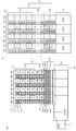
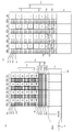
- FIG. 1 is a diagram for explaining a solid-state imaging device according to Embodiment 1 of the present invention, and shows an overall configuration of a CCD image sensor as the solid-state imaging device of Embodiment 1.
- FIG. 2 is a diagram for explaining the solid-state imaging device according to Embodiment 1 of the present invention.
- FIG. 2A shows an arrangement of transfer gates in the vertical transfer unit of the CCD image sensor shown in FIG. (B) shows the type of vertical transfer pulse applied to the transfer gate.
- FIG. 3 is a diagram for explaining the solid-state imaging device according to Embodiment 1 of the present invention.
- FIG. 1 is a diagram for explaining a solid-state imaging device according to Embodiment 1 of the present invention, and shows an overall configuration of a CCD image sensor as the solid-state imaging device of Embodiment 1.
- FIG. 2A shows an arrangement of
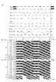
- FIG. 4 is a diagram for explaining the operation of the solid-state imaging device according to Embodiment 1 of the present invention.
- FIG. 4A shows the waveforms of vertical transfer pulses and horizontal transfer pulses in this solid-state imaging device.
- FIG. 4B and FIG. 4C are diagrams showing how transfer packets move as time passes on one and the other of the two vertical transfer units.
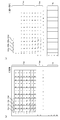
- FIG. 5 is a diagram for explaining the operation of the solid-state imaging device according to Embodiment 1 of the present invention.
- FIG. 5A shows an initial state in which signal charges of a color corresponding to each pixel in the Bayer array are accumulated.
- FIG. 5B shows a state in which signal charges are read from the pixels to the vertical transfer unit.
- FIG. 5A shows an initial state in which signal charges of a color corresponding to each pixel in the Bayer array are accumulated.
- FIG. 5B shows a state in which signal charges are read from the pixels to the vertical transfer unit.
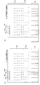
- FIG. 6 is a diagram for explaining the operation of the solid-state imaging device according to Embodiment 1 of the present invention.
- FIG. 6A illustrates the third column, the fourth column, the seventh column, the eighth column,
- FIG. 6B shows a state in which signal charges are transferred from the 11th and 12th column vertical transfer units to the horizontal transfer unit.
- FIG. 6B shows the signal charges transferred in this way for two columns of the vertical transfer unit in the horizontal direction. The state transferred to is shown.
- FIG. 7 is a diagram for explaining the operation of the solid-state imaging device according to Embodiment 1 of the present invention.
- FIG. 7A illustrates the first, second, fifth, sixth, FIG.
- FIG. 7B shows a state in which the signal charges are transferred from the ninth column and the tenth column from the vertical transfer unit to the horizontal transfer unit.
- FIG. 7B further illustrates the third column, the fourth column, the seventh column, The signal charges are transferred from the vertical transfer units in the eighth, eleventh, and twelfth columns to the horizontal transfer unit.
- FIG. 8 is a diagram for explaining the operation of the solid-state imaging device according to Embodiment 1 of the present invention.
- FIG. 8A shows signal charges corresponding to two columns of the vertical transfer unit from the state shown in FIG.
- FIG. 8B shows the vertical transfer unit in the first, second, fifth, sixth, ninth, ninth, and tenth columns from the left side of the drawing.
- FIG. 2 shows a state in which signal charges are transferred from the horizontal transfer unit to the horizontal transfer unit.
- FIG. 9 is a diagram for explaining a solid-state imaging device according to Embodiment 2 of the present invention, and shows the overall configuration of a CCD image sensor as the solid-state imaging device of Embodiment 2.
- FIG. 10 is a diagram for explaining a solid-state imaging device according to Embodiment 2 of the present invention.
- FIG. 10A shows the arrangement of transfer gates in the vertical transfer unit of the CCD image sensor shown in FIG. (B) shows the type of vertical transfer pulse applied to the transfer gate.
- FIG. 11 is a diagram for explaining a solid-state imaging device according to Embodiment 2 of the present invention.
- FIG. 12 is a diagram for explaining the operation of the solid-state imaging device according to Embodiment 2 of the present invention.
- FIG. 12A shows the waveforms of the vertical transfer pulse and the horizontal transfer pulse in this solid-state imaging device.
- FIG. 12B and FIG. 12C are diagrams showing how transfer packets move over time on one and the other of the two vertical transfer units.
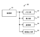
- FIG. 13 is a block diagram illustrating a schematic configuration example of an electronic information device using the solid-state imaging device according to any one of Embodiments 1 and 2 as an imaging unit as Embodiment 3 of the present invention.
- FIG. 12A shows the waveforms of the vertical transfer pulse and the horizontal transfer pulse in this solid-state imaging device.
- FIG. 12B and FIG. 12C are diagrams showing how transfer packets move over time on one and the other of the two vertical transfer units.
- FIG. 13 is a block diagram illustrating a schematic configuration example of an electronic information device using the solid-state imaging device according to any one of Embodiments 1 and 2 as
- FIG. 14 is a diagram for explaining a CCD image sensor as a conventional solid-state imaging device.
- FIG. 14A shows an arrangement of transfer gates in a vertical transfer unit of the CCD image sensor, and FIG. The type of vertical transfer pulse applied to the transfer gate is shown.
- FIG. 15 is a diagram for explaining the operation of a conventional solid-state imaging device, and FIGS. 15A to 15F show an initial state in which signal charges of colors corresponding to the pixels of the Bayer array are accumulated. This shows the movement of the signal charge until the signal charge is added in the transfer operation to the horizontal transfer unit.
- FIG. 1 shows the overall configuration of the CCD image sensor.
- the CCD image sensor 1 includes a pixel unit 1a that is formed on a semiconductor substrate (not shown) and includes a plurality of pixels PD arranged in a matrix (matrix). In each pixel PD, signal charges are generated by photoelectric conversion of incident light from a subject.
- a vertical transfer unit hereinafter also referred to as a VCCD unit
- a read gate Rg is arranged between the VCCD unit 100 and each pixel PD of the corresponding pixel column 10, and signal charges generated in each pixel PD are passed through the read gate Rg. The data is read out to the corresponding VCCD unit 100.
- the CCD image sensor 1 is disposed on one end side of the plurality of VCCD units 100 and horizontally transfers signal charges transferred from the VCCD units 100 in the horizontal direction (hereinafter also referred to as HCCD units). .) 1b, a charge detection unit 1d which is arranged on one end side of the HCCD unit 1b, detects a signal charge from the HCCD unit 1b and converts it into a voltage signal, and a voltage signal obtained by the charge detection unit 1d. And an output unit 1c that amplifies and outputs the pixel signal Sp to the output terminal CCDOUT.
- the CCD image sensor 1 generates vertical drive signals (vertical drive pulses) ⁇ V1 to ⁇ V4, ⁇ Vs1a, ⁇ Vs1b, ⁇ Vs2, ⁇ Vs3a, ⁇ Vs3b, and ⁇ Vs4 for driving the VCCD unit 100 and the HCCD unit 1b.
- a timing generation unit 111a that generates horizontal drive signals (horizontal drive pulses) ⁇ H1 and ⁇ H2 to be driven, and a signal charge generated by a pixel provided on the back side of the semiconductor substrate constituting the CCD image sensor 1 1, an overflow drain (hereinafter also referred to as an OFD unit) (not shown) discharged to the outside of 1 and a control signal for each of the timing generator 111 a and the overflow drain based on the pixel signal Sp from the output unit 1 c. Control by Ctg and Cofd And a control unit 111b. That is, here, the overflow drain portion draws out the signal charge generated in each pixel PD to the outside of the substrate by the control voltage Cofd applied thereto.
- FIG. 2A shows the arrangement of vertical transfer gates in the pixel portion of the CCD image sensor shown in FIG. 1, and FIG. 2B shows the types of vertical transfer pulses applied to the vertical transfer gates.
- the pixel portion 1a of the CCD image sensor 1 has pixels arranged therein, a transfer gate region (pixel gate portion) 1ac in which signal charges are read from the pixels and transferred in the vertical direction, and the pixels are arranged.
- the addition gate region 1as is provided between the transfer gate region 1ac and the HCCD unit 1b.
- the peripheral region 1a2 of the transfer gate region 1ac is a light-shielding region 1a2 shielded by a light-shielding film (not shown), and pixels located in the light-shielding region 1a2 are light-shielded pixels (OB) that are not subjected to photoelectric conversion. ).
- red pixels (R pixels) that generate signal charges of the red component, the green component, and the blue component of the subject light.
- a green pixel (G pixel), and a blue pixel (B pixel) which are in a Bayer array.
- the red pixel (R pixel), the green pixel (G pixel), and the blue pixel (B pixel) each have a configuration in which a color filter that transmits only light of each color component is disposed on the photodiode.
- the transfer gate located in the transfer gate region 1ac is a normal transfer gate constituting the pixel gate portion of the VCCD portion 100
- the transfer gate located in the addition gate region 1as is the addition gate portion of the VCCD portion 100. It is the transfer gate for addition which comprises.
- FIGS. 2 (a) and 2 (b) show only four pixel columns and VCCD units, that is, only pixel columns 10a to 10d and corresponding VCCD units 100a to 100d.
- four pixel columns and VCCD portions are repeatedly arranged, and a larger number of pixel rows and VCCD portions are provided according to the number of pixels.
- the first to fourth pixel columns 10a to 10d are arranged in the pixel unit 1a, and the first to fourth VCCD units 100a to 100d are arranged along each pixel column. Is arranged.
- the pixel columns 10a and 10c in the first column and the third column are pixel columns in which G pixels and R pixels are alternately arranged
- the pixel columns in the second column and the fourth column 10b and 10d are pixel columns in which B pixels and G pixels are alternately arranged, and pixels of the same color (green pixels) are not adjacent to each other between adjacent pixel columns.
- the VCCD portions 100a to 100d in the first to fourth columns corresponding to the pixels 10a to 10d are formed to extend from the transfer gate region 1ac to the addition gate region 1as, and constitute each VCCD portion.
- the transfer termination side of the vertical transfer channel 101 is connected to the horizontal transfer channel 102 constituting the HCCD unit 1b.
- transfer gates 111 to 114 are repeatedly arranged on each vertical transfer channel 101 so as to correspond to each pixel PD.
- addition gates four transfer gates for addition (hereinafter also referred to as addition gates) straddling two adjacent vertical transfer channels 101 are distances corresponding to two pixels along the vertical transfer direction. It is arranged repeatedly every time.
- four addition gates 121a to 124a are repeated twice along the vertical transfer direction so as to straddle the two vertical transfer channels 101 corresponding to the first and second pixel columns 10a and 10b.
- the four addition gates 121b to 124b are repeated twice along the vertical transfer direction so as to straddle the two vertical transfer channels 101 corresponding to 10c and 10d of the third and fourth pixel columns. Are arranged.
- a drive signal (vertical transfer pulse) is applied to the transfer gates 111 to 114 and the addition gates 121a to 124a and 121b to 124b.
- the transfer gates 111 to 114 of the VCCD unit are driven by four-phase vertical transfer pulses ⁇ V1 to ⁇ V4, and the first group addition gates 121a to 124a are driven by vertical transfer pulses ⁇ Vs1a, ⁇ Vs2, ⁇ Vs3a, and ⁇ Vs4.
- the addition gates 121b to 124b of the second group are driven by vertical transfer pulses ⁇ Vs1b, ⁇ Vs2, ⁇ Vs3b, and ⁇ Vs4.
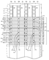
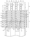
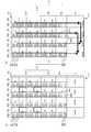
- FIG. 3 shows a structure (X1 portion in FIG. 2) in which the addition gate and its gate wiring are connected in the addition gate region (addition gate portion) of the VCCD portion shown in FIG.
- one period is described as a region (distance) in which the signal charge moves in one period of the vertical drive pulse and the horizontal drive pulse in both the vertical direction and the horizontal direction.
- the first to fourth addition gates 121a to 124a of the first group extend over two cycles so as to straddle the VCCD portions 100a and 100b in the first column and the second column.
- the first to fourth addition gates 121b to 124b of the second group are repeatedly arranged over two periods so as to straddle the VCCD sections 100c and 100d in the third and fourth columns. ing.
- the first to fourth addition gates 121a to 124a of the first group and the first to fourth addition gates 121b to 124b of the second group are at the same position (the same vertical transfer stage) in the vertical transfer direction. Is arranged.
- the first addition gate 121a of the first group and the first addition gate 121b of the second group are located in the same vertical transfer stage, and a pair of first gates is placed on these addition gates.
- the wirings W1a and W1b are arranged adjacent to each other, and the vertical transfer pulse ⁇ Vs1a is applied to one gate wiring W1a, and the vertical transfer pulse ⁇ Vs1b is applied to the other gate wiring W1b.
- the first addition gate 121a of the first group is connected to one gate wiring W1a by a contact hole C1a
- the first addition gate 121b of the second group is connected to the other gate wiring W1b by a contact hole C1b. Yes.
- a pair of second gate lines W2a and W2b are arranged on the first and second groups of second addition gates 122a and 122b located in the same vertical transfer stage, and these addition gates 122a. And 122b are connected to one gate wiring W2a to which the vertical transfer pulse ⁇ Vs2 is applied by a contact hole C2a.
- the third addition gate 123a of the first group and the third addition gate 123b of the second group are located in the same vertical transfer stage, and a pair of third gates are disposed on these addition gates.
- Wirings W3a and W3b are arranged, vertical transfer pulse ⁇ Vs3a is applied to one gate wiring W3a, and vertical transfer pulse ⁇ Vs3b is applied to the other gate wiring W3b.
- the third addition gate 123a of the first group is connected to one gate wiring W3a by a contact hole C3a
- the third addition gate 123b of the second group is connected to the other gate wiring W3b by a contact hole C3b. Yes.
- a pair of fourth gate lines W4a and W4b are arranged on the first and second groups of fourth addition gates 124a and 124b located in the same vertical transfer stage, and these addition gates 124a. And 124b are connected by a contact hole C4a to one gate wiring W4a to which the vertical transfer pulse ⁇ Vs4 is applied.
- connection between the first and second addition gates in the second period and the gate wiring adjacent to the HCCD unit is the same as the connection between the first and second addition gates in the first period and the gate wiring. It is.
- first gate wirings W5a and W5b are arranged adjacent to each other on the first addition gates 121a and 121b in the second period of the first and second groups, and the first group first
- the addition gate 121a is connected to the gate wiring W5a to which the vertical transfer pulse ⁇ Vs1a is applied by the contact hole C5a
- the first addition gate 121b of the second group is connected to the gate wiring W5b to which the vertical transfer pulse ⁇ Vs1b is applied. Connected by.
- the second addition gates 122a and 122b in the second period are connected to the gate wiring W6a to which the vertical transfer pulse ⁇ Vs2 is applied, of the pair of gate wirings W6a and W6b arranged above them, by the contact hole C6a. Has been.
- the third addition gates 123a and 123b in the second period of the first and second groups a pair of first gate wirings W7a and W7b are arranged adjacent to each other, and the third group of the first group
- the addition gate 123a is connected to the gate wiring W7a to which the vertical transfer pulse ⁇ Vs3a is applied through the contact hole C7a
- the third addition gate 123b in the second group has a contact hole C7b to the gate wiring W7b to which the vertical transfer pulse ⁇ Vs3b is applied. Connected by.
- the fourth addition gates 124a and 124b in the second period have contact holes connected to the gate wiring W8a to which the vertical transfer pulse ⁇ Vs4 is applied, of the pair of fourth gate wirings W8a and W8b arranged above them. Connected by C8a.
- this addition gate region (addition gate portion of the VCCD portion) 1as vertical transfer pulses independent of the first and third addition gates of the second group are applied to the first and third addition gates of the first group.
- the charge transfer timing to the HCCD unit 1b is changed from the third column and the fourth column of the VCCD units 100a and 100b to the HCCD unit.
- the timing can be different from the timing of transferring the signal charge to 1b, and this makes it possible to add the signal charge when transferring the signal charge from the VCCD unit to the HCCD unit.
- the gate wiring is, for example, a tungsten wiring
- the transfer gate and the addition gate are polysilicon gates.
- the addition gate is common to two adjacent VCCD units.
- the first to fourth addition gates 121a to 124a are connected to the first VCCD unit and the second VCCD unit.
- the first to fourth addition gates 121b to 124b are provided so as to straddle the third VCCD unit and the fourth VCCD unit, but the addition gates are independent for each VCCD unit. It is good also as a structure.
- the pixel columns 10a to 10d of the first column to the fourth column and the VCCD units 100a to 100d of the first column to the fourth column are not particularly distinguished if they do not need to be distinguished.
- the column 10 and the VCCD unit 100 will be described.
- the timing is The generating unit 111a generates vertical drive signals (vertical drive pulses) ⁇ V1 to ⁇ V4, ⁇ Vs1a, ⁇ Vs1b, ⁇ Vs2, ⁇ Vs3a, ⁇ Vs3b, and ⁇ Vs4 based on the control signal Ctg from the control unit 111b, and a horizontal drive signal ( Horizontal drive pulses) ⁇ H1 and ⁇ H2 are generated and output to the VCCD unit 100 and the HCCD unit 1b, respectively.
- vertical drive signals vertical drive pulses
- signal charges are generated in each pixel PD by photoelectric conversion of incident light, and the signal charges read from the pixel PD to the VCCD unit 100 via the read gate Rg are transferred to the HCCD unit 1b by the VCCD unit 100.
- the signal charges read from the VCCD unit 100 are transferred in the horizontal direction.
- the charge detection unit 1d disposed at the terminal end of the HCCD unit 1b detects the transferred signal charge, converts it into a voltage signal, and outputs the voltage signal to the output unit 1.
- the output unit 1 receives from the charge detection unit 1d.
- the output voltage signal is amplified and output as a pixel signal Sp.
- a camera angle with respect to a subject is determined in a monitoring mode in which a moving image is displayed on a liquid crystal monitor (not shown), and then a still image is captured by a shutter operation.
- the operation in the monitoring mode will be described.
- the monitoring mode (addition mode) of the solid-state imaging device 1 when the signal charges are read from the pixel row 10 corresponding to the VCCD unit 100, the arrangement of the signal charges is rearranged in the vertical direction. The signal charge is added when the signal charge is read from the unit to the HCCD unit.
- FIG. 4 is a diagram for explaining the operation of the solid-state imaging device according to the first embodiment.
- FIG. 4A is a vertical drive in the case of adding signal charges when reading signal charges from the VCCD unit to the HCCD unit.
- FIG. 4B and FIG. 4C show changes in transfer packets in the first and second group VCCD sections when this pixel addition is performed.
- FIG. 4 for convenience of explanation, only the VCCD unit 100a (FIG. 4B) and the VCCD unit 100c (FIG. 4C) of the VCCD units 100a to 100d are shown.
- FIG. 5A is an initial diagram in which signal charges of colors corresponding to the pixels of the Bayer array are accumulated.
- FIG. 5B shows a state in which the signal charges are transferred in the vertical direction up to the addition gate region by rearranging the order of the signal charges in the vertical direction.
- FIGS. 5A, 5B to 8A, 8B the light shielding region 1a2 shown in FIG. 2 and the pixels (OB) in this light shielding region are omitted for the sake of simplicity of explanation.
- the numbers (1 to 8) at the left end of FIG. 5 (a) indicate the pixel row numbers in the pixel portion in order from the closest to the HCCD portion, and the numbers (1 to 12) on the lower side of FIG.
- the numbers of the pixel columns in the pixel portion are shown in order from the left side of the drawing, and the numbers (1 to 8) at the left end of FIGS.
- FIG. 5 (b), 6 (a), (b) to 8 (a), (b) are The numbers of the vertical transfer stages in the pixel portion are shown in order from the one closest to the HCCD portion, and the numbers (1) below the FIG. 5 (b), FIG. 6 (a), (b) to FIG. 8 (a) and FIG. -12) indicate the column numbers of the VCCD portion in the pixel portion in order from the left side of the drawing.
- S indicates two vertical transfer stages in the addition gate region 1as.
- the solid-state imaging device 1 when light from a subject is incident on each pixel PD of the pixel unit 1a, the pixel PD of each of the pixel columns 10a to 10d has a corresponding color component as shown in FIG. Signal charge is generated and stored.
- signal charges are read from the pixel columns 10a to 10d to the corresponding VCCD units 100a to 100d.
- the signal charges are arranged in the same color in each of the VCCD units 100a to 100d.
- the signal charges generated in the pixels of the non-light-shielding region 1a1 of the transfer gate region 1ac are the most in the HCCD portion in the non-light-shielding region 1a1.
- the signal charge of the near pixel is transferred until it reaches the addition gate region (S) 1as.
- the signal charges in the first row and the second row of the (k) th and (k + 1) th (k is a natural number) VCCD units are represented by the (k + 2) th and (k + 3) th VCCD units.
- the signal charges held in the addition gate regions (addition gate portions) 1as of the VCCD portions 100a and 100b in the first column and the second column are left as they are.
- the signal charges held in the addition gate regions (addition gate units) 1as of the VCCD units 100c and 100d in the columns and the fourth column are read out to the HCCD unit 1b (FIG. 6A).
- FIG. 4A shows signal charges in the vertical transfer pulse waveform shown in FIG. 4A, signal charges are read out from the VCCD units 100c and 100d in the third and fourth columns during the timings t1 to t2, and FIG. c) shows a transfer packet (indicated by a black square in FIGS. 4B and 4C) formed in the transfer channel of the VCCD unit 100c in the third column between the timings t1 and t2. It shows how it changes.
- the signal charge [R13] shown in FIG. 5 (b) is held in the three transfer packets arranged vertically in the lower left corner of the diagram shown in FIG. 4 (c).
- a signal charge [R33] shown in FIG. 5B is stored in three transfer packets arranged vertically in the upper side of the packet.
- the transfer packet storing these signal charges moves to the HCCD unit 1b side during the timings t1 to t2, and these signal charges [R13] and [R33] are shown in FIG. As shown, it is read into the HCCD unit 1b.
- the signal charges [G14] and [G34] are read from the VCCD unit 100d in the fourth column into the HCCD unit 1b as shown in FIG. 6A.
- the signal charge [R11] shown in FIG. 5 (b) is held in the two vertically aligned transfer packets shown in the lower left corner of the diagram shown in FIG. 4 (b).
- a signal charge [R31] shown in FIG. 5B is stored in two vertically aligned transfer packets located above these two transfer packets.
- the transfer packet storing these signal charges repeats backward and forward twice between the timings t1 and t2. For this reason, these signal charges [R11] and [R31] remain in the addition gate region 1as of the VCCD portion as shown in FIG. 6 (a) between timings t1 and t2.
- the signal charges read out to the HCCD unit 1b in this way are transferred by two cycles in the horizontal direction as shown in FIG. 6B by the horizontal drive pulses ⁇ H1 and ⁇ H2 shown in FIG. (Timing t2).
- the first VCCD unit Signal charges are transferred from the 100a and the second VCCD unit 100b to the HCCD unit 1b. Thereby, signal charges [R13], [R33], [R11] and [R31] are added, and signal charges [G14], [G34], [G12] and [G32] are added.
- the signal charges held in the addition gate regions 1as of the VCCD units 100a and 100b in the first column and the second column remain as they are during the timing t3 to t4.
- the signal charges held in the addition gate regions 1as of the VCCD units 100c and 100d in the third and fourth columns are read out to the HCCD unit 1b. That is, the signal charges [G23] and [G43] are read from the VCCD unit 100c in the third column into the HCCD unit 1b as shown in FIG. 7B, and the VCCD unit 100d in the fourth column.
- the signal charges [B24] and [B44] are read out from the HCCD unit 1b as shown in FIG.
- the signal charges read out to the HCCD unit 1b in this way are transferred by two cycles in the horizontal direction as shown in FIG. 8A by the horizontal drive pulses ⁇ H1 and ⁇ H2 shown in FIG. (Timing t4).
- the first VCCD unit Signal charges are transferred from the 100a and the second VCCD unit 100b to the HCCD unit 1b. Thereby, signal charges [G23], [G43], [G21] and [G41] are added, and signal charges [B24], [B44], [B22] and [B42] are added.
- control unit 111b controls the transfer operation of the VCCD unit in the still mode by the shutter operation signal.
- control unit 111b converts the vertical transfer pulses ⁇ V1 to ⁇ V4, ⁇ Vs1a, ⁇ Vs1b, ⁇ Vs2, ⁇ Vs3a, ⁇ Vs3b, and ⁇ Vs4 into waveforms when the signal charges are vertically transferred in all the VCCD units. Normal transfer operation is performed. Thereby, the transfer of the signal charge from the VCCD unit to the HCCD unit is performed without adding the signal charge.
- the CCD image sensor 1 having the plurality of pixels PD arranged in a matrix includes the four-phase drive vertical transfer unit (VCCD unit) 100 provided for each pixel column, In the addition gate unit (addition gate region) 1as adjacent to the horizontal transfer unit (HCCD unit) 1b of the VCCD unit 100, the first and fourth of the first to fourth addition gates 121a to 124a, 121b to 124b. 3 transfer gates, VCCD units 100a and 100b in the first column (k column), second column (k + 1 column) (k: natural number), third column (k + 2 column), and fourth column (k + 3).
- the VCCD units 100c and 100d in the first column are driven by separate vertical transfer pulses, for example, the addition gate region 1a of the VCCD units 100a and 100b in the first and second columns. Transfer of signal charges from the first to the HCCD unit 1b can be delayed from the transfer of signal charges from the addition gate regions 1as of the third and fourth VCCD units 100c and 100d to the HCCD unit 1b. Thus, when the signal charges are transferred from the VCCD unit 100 to the HCCD unit, the signal charges of the same color pixels can be added.
- the addition gate unit (addition gate region) 1as in the VCCD unit 100 uses the first to first groups of transfer gates common to the first and second VCCD units 100a and 100b.
- Two sets of fourth addition gates 121a to 124a are repeatedly arranged, and the second group of first to fourth addition gates 121b to 124b are used as transfer gates common to the VCCD units 100c and 100d in the third and fourth columns.
- a pair of gate wirings (for example, gate wirings W1a and W1b) straddling two addition gates (for example, the addition gate 121a and the addition gate 121b) corresponding to the same vertical transfer stage in each group. Therefore, each summing gate is in contact with one of a pair of gate wirings located above it through a contact hole. It can become.
- the signal charges that can be transferred are transferred signals corresponding to one pixel in the pixel gate portion (transfer gate region) 1ac of the VCCD portion.
- the signal charge amount can be the same as the charge amount, and a large range can be secured as the dynamic range of the pixel signal.
- the gate length (that is, the size of the transfer gate in the transfer direction) in the addition gate region 1as of the VCCD unit 100 is made equal to the gate length in the transfer gate region 1ac other than the addition gate region. Therefore, it can be avoided that the transfer speed in the transfer gate region of the VCCD section and the amount of signal charge that can be transferred are limited by the gate length in the addition gate region.
- the addition gate region 1as in the first embodiment, as can be seen from FIGS. 4B and 4C, signal charges are held by two addition gates (that is, two transfer packets). Therefore, the addition gate region 1as can transfer the same amount of signal charge as the amount of signal charge handled in the pixel gate portion 1ac of the VCCD portion in both the normal mode and the addition mode.
- the CCD image sensor 2 according to the second embodiment includes a pixel portion 2a having a different configuration for adding signal charges in place of the pixel portion 1a in the CCD image sensor 1 according to the first embodiment.
- a transfer unit (VCCD unit) 100, a vertical transfer unit (VCCD unit) 200 instead of the timing generation unit 111a and the control unit 111b, a timing generation unit (TG) 211a, and a control unit 211b are provided.
- FIG. 10A shows the arrangement of the vertical transfer gates in the pixel portion 2a of the CCD image sensor 2 of the second embodiment shown in FIG. 9, and FIG. 10B shows the types of vertical transfer signals applied to the vertical transfer gates. Is shown.
- FIG. 10 (a) and FIG. 10 (b) four pixel columns and VCCD sections, that is, pixel columns 10a to 10d and corresponding VCCD sections 200a to 200d.
- four pixel columns and VCCD units are repeatedly arranged, and a larger number of pixel columns and VCCD units are provided according to the number of pixels.
- the pixel column 10 and the VCCD unit 200 will be described.
- the pixel unit 2a of the CCD image sensor 2 reads out signal charges from each pixel and transfers them in the vertical direction.
- the transfer gate region (pixel gate portion) 1ac composed of the light shielding region 1a2 and the HCCD portion 1b so that the pixels are not arranged and signal charges from a plurality of pixels are added or not added.
- transfer gates 111 to 114 are repeatedly arranged on each vertical transfer channel 101 so as to correspond to each pixel PD.
- two dummy gates are arranged along the vertical transfer direction, and in the addition gate region 2as adjacent to the dummy gate region 2ad, the two dummy gates follow.
- Three addition gates are arranged twice.
- two dummy gates 121c and 122c are arranged along the vertical transfer direction so as to straddle the two vertical transfer channels 101 corresponding to the first and second pixel columns 10a and 10b.
- three addition gates 221 a to 223 a are repeatedly arranged twice along the vertical transfer direction so as to straddle the two vertical transfer channels 101.
- Two dummy gates 121d and 122d are arranged along the vertical transfer direction so as to straddle the two vertical transfer channels 101 corresponding to the third and fourth pixel columns 10c and 10d.
- the addition gates 221b to 223b are repeatedly arranged twice along the vertical transfer direction so as to straddle the two vertical transfer channels 101.
- a drive signal (vertical transfer pulse) is applied to each of the transfer gates 111 to 114, the dummy gates 121c and 122c, and the addition gates 221a to 223a and 221b to 223b. It has become.
- the transfer gates 111 and 112 of the VCCD unit are driven by the vertical transfer pulses ⁇ V3 and ⁇ V4 of the four-phase vertical transfer pulses ⁇ V1 to ⁇ V4, and the transfer gates 113 and 114 of the VCCD unit are driven by the four-phase vertical transfer pulses ⁇ V1 to ⁇ V1. It is driven by vertical transfer pulses ⁇ V1 and ⁇ V2 of ⁇ V4.
- the dummy gates 121c and 121d are driven by the vertical transfer pulse ⁇ V3, and the dummy gates 122c and 122d are driven by the vertical transfer pulse ⁇ V4.
- addition gates 221a to 223a of the first group are driven by vertical transfer pulses ⁇ Vs1a to ⁇ Vs3a
- addition gates 221b to 223b of the second group are driven by vertical transfer pulses ⁇ Vs1b to ⁇ Vs3b.
- FIG. 11 shows a structure (X2 portion in FIG. 10A) in which the dummy gate and the addition gate are connected to the gate wiring in the dummy gate region and the addition gate region of the VCCD portion shown in FIG.
- the first and second dummy gates 121c and 122c of the first group are arranged so as to straddle the VCCD portions 200a and 200b in the first column and the second column.
- the first group addition gates 221a to 223a are repeatedly arranged twice.
- the second group of first and second dummy gates 121d and 122d are arranged so as to straddle the third and fourth columns of the VCCD sections 200c and 200d, and the second group of addition gates 221b to 223b. Are arranged twice.
- first and second dummy gates of the first group and the first and second dummy gates of the second group are arranged at the same position (vertical transfer stage) in the vertical transfer direction.
- the first to third addition gates of the first group and the first to third addition gates of the second group are arranged at the same position (vertical transfer stage) in the vertical transfer direction.
- the first dummy gate 121c of the first group and the first dummy gate 121d of the second group are located in the same vertical transfer stage, and a pair of first gate wirings W1a is disposed on these dummy gates. And W1b are arranged adjacent to each other, and the vertical transfer pulse ⁇ V3 is applied to one gate wiring W1a, and the vertical transfer pulse is not applied to the other gate wiring W1b.
- the first dummy gate 121c of the first group is connected to one gate wiring W1a via a contact hole C1a
- the first dummy gate 121d of the second group is similarly connected to the gate wiring W1a via a contact hole C1b. ing.
- the second dummy gate 122c of the first group and the second dummy gate 122d of the second group are located in the same vertical transfer stage, and a pair of first gates are disposed on these dummy gates.
- the wirings W2a and W2b are arranged adjacent to each other, and the vertical transfer pulse ⁇ V4 is applied to one of the gate wirings W2a, and the vertical transfer pulse is not applied to the other gate wiring W2b.
- the second dummy gate 122c of the first group is connected to one gate wiring W2a by a contact hole C2a
- the second dummy gate 122d of the second group is similarly connected to the gate wiring W2a by a contact hole C2b. ing.
- the first addition gate 221a of the first group and the first addition gate 221b of the second group are located in the same vertical transfer stage, and a pair of third gates is placed on these addition gates.
- the wirings W3a and W3b are arranged adjacent to each other, and the vertical transfer pulse ⁇ Vs1a is applied to one of the gate wirings W3a, and the vertical transfer pulse ⁇ Vs1b is applied to the other gate wiring W3b.
- the first addition gate 221a of the first group is connected to one gate wiring W3a by a contact hole C3a
- the first addition gate 221b of the second group is connected to the other gate wiring W3b by a contact hole C3b. ing.
- the second addition gate 222a of the first group and the second addition gate 222b of the second group are located in the same vertical transfer stage, and a pair of fourth gates are disposed on these addition gates.
- Wirings W4a and W4b are arranged adjacent to each other, vertical transfer pulse ⁇ Vs2a is applied to one gate wiring W4a, and vertical transfer pulse ⁇ Vs2b is applied to the other gate wiring W4b.
- the second addition gate 222a of the first group is connected to one gate wiring W4a by a contact hole C4a
- the second addition gate 222b of the second group is connected to the other gate wiring W4b by a contact hole C4b. ing.
- the third addition gate 223a of the first group and the third addition gate 223b of the second group are located in the same vertical transfer stage, and a pair of fifth gates is disposed on these addition gates.
- Wirings W5a and W5b are arranged adjacent to each other, and vertical transfer pulse ⁇ Vs3a is applied to one gate wiring W5a, and vertical transfer pulse ⁇ Vs3b is applied to the other gate wiring W5b.
- the third addition gate 223a of the first group is connected to one gate wiring W5a by a contact hole C5a
- the third addition gate 223b of the second group is connected to the other gate wiring W5b by a contact hole C5b. ing.
- the three addition gates 221a to 223a and 221b to 223b in the second period arranged in the vertical transfer direction following the three addition gates 221a to 223a and 221b to 223b are the same as those in the first period. Is connected to the gate wiring.
- the first addition gate 221a of the first group and the first addition gate 221b of the second group are located in the same vertical transfer stage, and a pair of sixth gates is placed on these addition gates.
- Wirings W6a and W6b are arranged adjacent to each other, and vertical transfer pulse ⁇ Vs1a is applied to one gate wiring W6a, and vertical transfer pulse ⁇ Vs1b is applied to the other gate wiring W6b.
- the first addition gate 221a of the first group is connected to one gate wiring W6a by a contact hole C6a
- the first addition gate 221b of the second group is connected to the other gate wiring W6b by a contact hole C6b. ing.
- the second addition gate 222a of the first group and the second addition gate 222b of the second group are located in the same vertical transfer stage, and a pair of seventh gates is disposed on these addition gates.
- the wirings W7a and W7b are arranged adjacent to each other, and the vertical transfer pulse ⁇ Vs2a is applied to one of the gate wirings W7a, and the vertical transfer pulse ⁇ Vs2b is applied to the other gate wiring W7b.
- the second addition gate 222a of the first group is connected to one gate wiring W7a by a contact hole C7a
- the second addition gate 222b of the second group is connected to the other gate wiring W7b by a contact hole C7b. ing.
- the third group of third addition gates 223a and the second group of third addition gates 223b are located in the same vertical transfer stage, and a pair of eighth gates is provided on these addition gates.
- Wirings W8a and W8b are arranged adjacent to each other, vertical transfer pulse ⁇ Vs3a is applied to one gate wiring W8a, and vertical transfer pulse ⁇ Vs3b is applied to the other gate wiring W8b.
- the third addition gate 223a of the first group is connected to one gate wiring W8a by a contact hole C8a
- the third addition gate 223b of the second group is connected to the other gate wiring W8b by a contact hole C8b. ing.
- the first to first addition gates 221a to 223a of the first group include the first to third units of the second group. Since vertical transfer pulses independent of the third addition gates 221b to 223b are applied, the VCCD units 200a and 200b in the first column and the second column have the timing of transferring charges to the HCCD unit 1b as the third timing.
- the timing of transferring signal charges from the VCCD units 200c and 200d in the columns and the fourth column to the HCCD unit 1b can be set to be different from the timing of transferring the signal charges from the VCCD units 200a to 200d to the HCCD unit 1b. In this case, signal charges can be added.
- the timing generation unit 211a In the CCD image sensor 2, the timing generation unit 211a generates vertical drive signals (vertical drive pulses) ⁇ V1 to ⁇ V4, ⁇ Vs1a to ⁇ Vs3a, and ⁇ Vs1b to ⁇ Vs3b that drive the VCCD unit 200, and the HCCD unit 1b. Are generated to generate horizontal drive signals (horizontal drive pulses) ⁇ H1 and ⁇ H2 for driving the control signal, and the control unit 211b controls the timing generation unit 211a and the overflow drain by control signals Ctg and Cofd, respectively. It is configured.
- the generator 211a when an operation signal from an operator instructing the start of an imaging operation is input to the control unit 211b and the control signal Ctg is supplied from the control unit 211b to the timing generation unit 211a,
- the generator 211a generates vertical drive pulses ⁇ V1 to ⁇ V4, ⁇ Vs1a to ⁇ Vs3a, and ⁇ Vs1b to ⁇ Vs3b based on the control signal Ctg from the controller 211b, and generates horizontal drive pulses ⁇ H1 and ⁇ H2, respectively.
- signal charges are generated by photoelectric conversion of incident light in each pixel PD, and the signal charges read from the pixel PD to the VCCD unit 200 via the read gate Rg are transferred to the HCCD unit 1b by the VCCD unit 200.
- the signal charges from the VCCD unit 200 are transferred in the horizontal direction in the HCCD unit 1b.
- the charge detection unit 1d arranged at the terminal end of the HCCD unit 1b detects the transferred signal charge, converts it into a voltage signal, and outputs it to the output unit 1c.
- the output unit 1c is connected to the charge detection unit 1d.
- the output voltage signal is amplified and output as a pixel signal Sp.
- the solid-state imaging device 2 of the second embodiment in the monitoring mode, when the signal charges are read out from the pixel column corresponding to the VCCD unit, the arrangement of the signal charges in the vertical direction is performed, and further, from the VCCD unit to the HCCD unit. The signal charge is added when the signal charge is transferred to.
- FIG. 12 is a diagram for explaining the operation of the solid-state imaging device according to the second embodiment.
- FIG. 12A is a vertical diagram in the case of adding signal charges when transferring signal charges from the VCCD unit to the HCCD unit.
- FIG. 12B and FIG. 12C show changes in transfer packets in the first and second group VCCD sections when the signal charges are added.
- FIGS. 5 to 8 used in the description of the operation of the first embodiment are used.
- the reference numeral “1as” indicating the addition gate region in FIGS. 5 to 8 is replaced with “2as”, and the reference numerals “100a to 100d” indicating the VCCD portion in FIGS. 200d ".
- FIG. 12 for convenience of explanation, only the VCCD unit 200a (FIG. 12B) and the VCCD unit 200c (FIG. 12C) of the VCCD units 200a to 200d are shown.
- the signal charges in the first row and the second row of the (k) th and (k + 1) th (k is a natural number) VCCD units are represented by the (k + 2) th and (k + 3) th VCCD units.
- the operation of adding the signal charges of the first and second rows will be specifically described using the signal charges of the first to fourth VCCD units 200a to 200d.
- the signal charges held in the addition gate regions (S) (addition gate portions) 2as of the VCCD portions 200a and 200b in the first and second columns remain as they are.
- the signal charges held in the addition gate regions (S) (addition gate portions) 2as of the VCCD portions 200c and 200d in the third and fourth columns are read out to the HCCD portion 1b (FIG. 6A). ).
- the signal charge [R13] shown in FIG. 5B is held in the two transfer packets arranged vertically in the lower left corner of the diagram shown in FIG. 12C, and these two transfer packets are stored.
- the signal charge [R33] shown in FIG. 5 (b) is stored in the two transfer packets arranged in the vertical direction on the upper side.
- the transfer packet storing these signal charges moves to the HCCD unit 1b side during the timings t1 to t2, and these signal charges [R13] and [R33] are shown in FIG. As shown, it is read into the HCCD unit 1b.
- the signal charges [G14] and [G34] are read out from the VCCD unit 200d in the fourth column into the HCCD unit 1b as shown in FIG. 6A.
- the signal charge [R11] shown in FIG. 5 (b) is held in the two transfer packets arranged vertically in the lower left corner of the diagram shown in FIG. 12 (b).
- the signal charge [R31] shown in FIG. 5B is stored in the two transfer packets arranged vertically, which are located above these two transfer packets.
- the transfer packet storing these signal charges does not move between the timings t1 and t2. For this reason, these signal charges [R11] and [R31] remain in the addition gate region 2as of the VCCD portion as shown in FIG. 6 (a) between the timings t1 and t2.
- the signal charges read out to the HCCD unit 1b in this way are transferred by two cycles in the horizontal direction as shown in FIG. 6B by the HCCD drive signals ⁇ H1 and ⁇ H2 shown in FIG. (Timing t2).
- the first VCCD unit Signal charges are transferred to the HCCD unit 1b from the 200a and the second VCCD unit 200b. Thereby, signal charges [R13], [R33], [R11] and [R31] are added, and signal charges [G14], [G34], [G12] and [G32] are added.
- the signal charges held in the addition gate regions (S) 2as of the VCCD units 200c and 200d in the third column and the fourth column are read out to the HCCD unit 1b while the charges remain unchanged. That is, the signal charges [G23] and [G43] are read from the third row VCCD unit 200c into the HCCD unit 1b as shown in FIG. 7B, and the fourth column VCCD unit 200d.
- the signal charges [B24] and [B44] are read out from the HCCD unit 1b as shown in FIG.
- the signal charges read out to the HCCD unit 1b in this way are transferred by two cycles in the horizontal direction as shown in FIG. 8A by the HCCD drive signals ⁇ H1 and ⁇ H2 shown in FIG. (Timing t4).
- the first VCCD unit Signal charges are transferred to the HCCD unit 1b from the 200a and the second VCCD unit 200b. Thereby, signal charges [G23], [G43], [G21] and [G41] are added, and signal charges [B24], [B44], [B22] and [B42] are added.
- control unit 211b controls the transfer operation of the VCCD unit in the still mode by the shutter operation signal.
- control unit 211b changes the vertical transfer pulses ⁇ V1 to ⁇ V4, ⁇ Vs1a to ⁇ Vs3a, and ⁇ Vs1b to ⁇ Vs3b to waveforms when the signal charges are vertically transferred in all the VCCD units, so that the normal transfer operation can be performed in the VCCD unit. Done. Thereby, the transfer of the signal charge from the VCCD unit to the HCCD unit is performed without adding the signal charge.
- the group of gate drive pulses applied to the addition gate is switched by connecting the addition gate and gate wiring of the VCCD unit.
- the signal charge corresponding to each pixel can be selected to be transferred by two transfer packets or by one transfer packet.
- the signal charge addition method is the same as the conventional method, but priority is given to the magnitude of the handled signal charge by switching the gate wiring connected to the addition gate, that is, by switching the timing of the drive signal applied to the addition gate. Or giving priority to the transfer speed, it is possible to provide a solid-state imaging device with higher performance and efficiency.
- the vertical lengths (gate lengths) of the addition gates 221a to 223a and 221b to 223b constituting the addition gate unit are shared by a plurality of VCCD units. Due to the gate length of the summing gate constituting the summing gate portion, it is possible to avoid the restriction on the amount of signal charges or the transfer speed handled by other VCCD portions.
- the last six addition gates are connected to the first group (kth and k + 1).
- the second CCDC section and the second group (k + 2 and k + 3) VCCD sections are independently driven to add signal charges when transferring signal charges to the HCCD sections. There is an effect that the transfer to the HCCD unit can be performed at a higher speed.
- the signal charge is held by one addition gate (that is, one transfer packet).
- the addition gates are driven completely independently by the first group (k-th and k + 1-th) VCCD units and the second group (k + 2-th and k + 3-th) VCCD units, the addition of the VCCD unit
- the gate portion (addition gate region) 2as in the normal mode, signal charges can be transferred in accordance with the transfer speed of the pixel gate portion (transfer gate region) 1ac of the VCCD portion. Signal charges can be transferred at high speed.
- FIG. 13 is a block diagram illustrating a schematic configuration example of an electronic information device using the solid-state imaging device of Embodiment 1 or 2 as an imaging unit as Embodiment 3 of the present invention.
- An electronic information device 90 according to Embodiment 3 of the present invention shown in FIG. 13 includes at least one of the solid-state imaging devices according to Embodiments 1 and 2 of the present invention as an imaging unit 91 that captures a subject.
- a memory unit 92 such as a recording medium for recording data after high-definition image data obtained by photographing by such an image pickup unit is subjected to predetermined signal processing for recording, and predetermined signal processing for displaying the image data
- a display unit 93 such as a liquid crystal display device that displays on a display screen such as a liquid crystal display screen, and a communication unit 94 such as a transmission / reception device that performs communication processing after performing predetermined signal processing on the image data for communication.
- an image output unit 95 that prints (prints) image data and outputs (prints out) the image data.
- the present invention relates to a transfer of signal charges from a vertical transfer unit to a horizontal transfer unit in a field of a solid-state imaging device, a driving method thereof, and an electronic information device, and a vertical transfer unit corresponding to a specific pixel column and another pixel column.
- the vertical transfer can be performed independently with the vertical transfer unit corresponding to the above, and the entire vertical transfer of the pixel unit without being restricted by the configuration that enables the transfer of the independent signal charge. It is possible to realize a solid-state imaging device capable of securing a signal charge amount that can be transferred at a speed or vertically, a driving method thereof, and an electronic information device including such a solid-state imaging device.
Landscapes
- Engineering & Computer Science (AREA)
- Multimedia (AREA)
- Signal Processing (AREA)
- Solid State Image Pick-Up Elements (AREA)
Abstract
通常モードおよび加算モードを有するCCDイメージセンサとして、垂直転送部(VCCD部)で取り扱う信号電荷の量を優先するか、垂直転送部での信号電荷の転送速度を優先するかを配線工程で選択でき、その用途に応じて、より性能の高い、効率の良いCCDイメージセンサを得る。加算モードではVCCD部からHCCD部へ信号電荷を転送する際に信号電荷の加算を行う加算ゲート部1asを有するCCDイメージセンサ1において、1列目、2列目のVCCD部100a、100bに共通する第1グループの加算ゲート121a~124aと、3列目、4列目のVCCD部100c、100dに共通する第2グループの加算ゲート121b~124bとを備え、各グループの同一垂直転送段に位置する加算ゲート上に跨るように、一対のゲート配線W1a、W1b~W8a、W8bを配置した。
Description
本発明は、固体撮像装置およびその駆動方法、並びに電子情報機器に関し、特に、静止画および動画の撮像を可能とした固体撮像装置において、垂直転送部から水平転送部へ信号電荷を転送する際に信号電荷の加算を行う動作モードを有するもの、このような固体撮像装置の駆動方法、並びにこのような固体撮像装置を備えた電子情報機器に関するものである。
従来から固体撮像装置にはCMOSイメージセンサやCCDイメージセンサがあり、これらのイメージセンサはデジタルスチルカメラやビデオカメラなどの撮像デバイスとして用いられている。いずれのイメージセンサも、被写体からの光を光電変換する素子としてフォトダイオードを用いているが、これらのイメージセンサは、フォトダイオードで得られた信号電荷をイメージセンサの外部に各画素に対応する画像信号(以下、画素信号という。)として取り出す方式が異なる。つまり、CCDイメージセンサでは、垂直転送部(垂直CCD)と水平転送部(水平CCD)を使って信号電荷を1つの出力部に転送し、この出力部で信号電荷を電圧信号に変換し増幅して画素信号として出力するのに対して、CMOSイメージセンサではフォトダイオード毎に信号電荷を電圧信号に変換し増幅して画素信号として出力する。
ところで、近年、デジタルスチルカメラの高画質化が急速に進んでおり、1000万画素以上の画素数を有する固体撮像装置、特にCCDイメージセンサが、広く使われるようになっている。これらのCCDイメージセンサにおいては、全画素の信号電荷を独立に読み出すことによって静止画が得られるように垂直CCDおよび水平CCDを駆動する動作モード(スチルモード)と、液晶モニター等に動画を映し出すための画像信号が得られるように垂直CCDおよび水平CCDを駆動する動作モード(モニタリングモード)とを切り替えて用いることが一般的である。
このようなモニタリングモードでは、毎秒30枚程度のフレームレートで画素信号を読み出す必要があるが、CCDイメージセンサの駆動周波数特性の限界あるいは低消費電力化という観点から駆動周波数を高速にすることができず、CCDイメージセンサの多画素化に伴ってモニタリングモードでのフレームレートの確保が困難になってくる。
これに対しては、現在一般的に、130万画素以上の画素数を有するCCDイメージセンサにおいては、主に以下の二つの方法でフレームレートの向上を図っている。
ひとつの方法としては、水平CCDと出力部を複数設けることで、個々の画素に対応する画素信号を出力する周波数を減少させ、これによりフレームレートを向上させる方法である。
これは、特許文献1に開示の水平2線読み出し方式CCDのように、垂直CCDからの各画素に対応する信号電荷を2つの水平CCDへ配分して2つの出力部から画素信号として出力させることによって、駆動周波数を上げなくても2倍のスピードのフレームレートを実現することができるものである。
しかし、上記特許文献1に開示の方法は、出力部の増加による信号処理部のコスト増大を招くため実用的ではない。
ふたつ目の方法としては任意の複数の画素からの信号電荷を加算することにより、データ量、つまり画素値として転送すべき信号電荷の個数を減少させることでフレームレートを向上させる方法である。
これは、特許文献2などに開示の画素加算方式CCDのように、任意の複数の信号電荷を混合して1画素の画像情報に圧縮する方法であり、画像情報の圧縮率が高いほど、つまり信号電荷を混合する画素の数が多いほど、フレームレートが向上していくというものである。
以下、このような信号電荷の加算(以下、画素加算ともいう。)によって画像情報を圧縮してフレームレートを向上させる方法について説明する。
図14は、従来の固体撮像装置であるCCDイメージセンサを説明する図であり、図14(a)は、このCCDイメージセンサの画素列および対応する垂直転送部の配列を示し、図14(b)では、垂直転送部から水平転送部への信号電荷の流れを示している。
このCCDイメージセンサ5は、行列状に配列された複数の画素PDを含む画素部5aを有し、さらに、複数の画素の各画素列に対応して設けられ、対応する画素列の画素からの信号電荷を垂直方向に転送する垂直転送部(VCCD部)500a~500dと、これらのVCCD部500a~500dの転送終端側に設けられ、各VCCD部からの信号電荷を水平方向に転送する水平転送部(HCCD部)1bとを有している。ここで、VCCD部500a~500dは、動作モードとして、信号電荷をHCCD部1bへ転送する際に信号電荷の加算を行う加算モード(モニタリングモード)と、信号電荷の加算を行わずに信号電荷をHCCD部1bへ転送する通常モード(スチルモード)とを有している。
また、画素部5aは、動作モードに拘わらず、信号電荷の転送をすべてのVCCD部500a~500dで同じタイミングで行う画素ゲート部(転送ゲート領域)5acと、信号電荷を一部のVCCD部500aおよび500bと他のVCCD部500cおよび500dとで異なる転送タイミングで転送可能に構成され、駆動信号により加算モードと通常モードとが切り換わる加算ゲート部(加算ゲート領域)5asとを有し、加算ゲート部5asは、HCCD部1bに隣接して位置している。
また、上記画素部5aの転送ゲート領域5acには、VCCD部500a~500dの、HCCD部1b側の遮光された遮光領域5a2と、この遮光領域5a2以外の、遮光されていない非遮光領域5a1とが配置されている。
なお、図14(a)および図14(b)では、説明の都合上、第1列目~第4列目の画素列50a~50d、およびこれらに対応する第1列目~第4列目のVCCD部500a~500dのみを示しているが、実際のCCDイメージセンサでは、画素列およびVCCD部は4列のみではなく、画素数に応じたより多くの列を含んでいる。また、各画素にはカラーフィルタが設けられており、赤色画素(R)、緑色画素(G)、および青色画素(B)の配列はベイヤー配列となっている。
ここで、第1列目のVCCD部500aの転送ゲート領域5acでは、対応する画素列50aの画素PD毎に4枚の通常の転送ゲート501~504が垂直方向に沿って配置されており、また、第1列目のVCCD部500aの加算ゲート領域5asでは、4枚の通常の転送ゲート(以下、単に転送ゲートともいう。)501~504および2枚の加算用の転送ゲート(以下、加算ゲートともいう。)505、506が垂直転送方向に沿って配置されている。また、第2列目のVCCD部500bにおける転送ゲートおよび加算ゲートの配列は、第1列目のVCCD部500aと全く同一となっている。
また、第3列目のVCCD部500cの画素ゲート部5acでは、対応する画素列50cの画素PD毎に4枚の転送ゲート501~504が垂直方向に沿って配置されており、また、第3列目のVCCD部500cの加算ゲート部5asでは、2枚の転送ゲート501、502と、2枚の加算用の転送ゲート(以下、加算ゲートともいう。)503a、504aとが、垂直方向に沿って配置されている。ここで、加算用の転送ゲート503aおよび504aは、転送方向の長さが通常の転送ゲート503および504の2倍となっている。
また、転送ゲート501~504には駆動信号として垂直転送パルスΦV1~ΦV4が印加され、また、加算ゲート503a、504aには駆動信号として垂直転送パルスΦV3、ΦV4が印加され、さらに、加算ゲート505および506には、垂直転送パルスΦV1~ΦV4とは独立した垂直転送パルスΦVs5およびΦVs6が印加されるようになっている。
次に動作について説明する。
このような構成のCCDイメージセンサ5では、垂直転送パルスΦV1~ΦV4を転送ゲート501~504、および加算ゲート503a、504aに印加することで、第3および第4番目のVCCD部500cおよび500dでは、図14(b)に実線の矢印で示すように、各画素の信号電荷が順番にHCCD部1bに転送され、さらに2相の水平転送パルス(図示せず)で駆動されるHCCD部1bを水平方向に転送されることとなる。
一方、第1および第2番目のVCCD部500aおよび500bでは、図14(b)に点線の矢印で示すように、各画素の信号電荷が順番にHCCD部1bに転送されることとなるが、このとき、HCCD部1bに隣接する部分の加算ゲート505および506には、垂直転送パルスΦV1~ΦV4とは独立した垂直転送パルスΦVs5およびΦVs6を印加して、第3番目および第4番目のVCCD部500cおよび500dからHCCD部1bに転送された信号電荷が、第1番目および第2番目のVCCD部500aおよび500bに対応する位置に転送されてくるまで、第1番目および第2番目のVCCD部500aおよび500bからHCCD部1bに信号電荷が転送されないようにする。
これにより、VCCD部500a~500dからHCCD部1bに信号電荷を転送する際に、第1番目および第2番目のVCCD部500aおよび500bからの信号電荷を、第3番目および第4番目のVCCD部500cおよび500dからの信号電荷と加算することができる。
以下、図15を用いて具体的に説明する。
まず、VCCD部500a~500dからHCCD部1bに信号電荷を転送する直前の初期状態で、VCCD部500a~500dの電荷転送パケット(以下、転送パケットと略記する。)には、図15(a)に示すように対応する画素列50a~50dから読み出された信号電荷(R)、(G)、(B)が蓄積されているとする。
この状態で、垂直転送パルスΦV1~ΦV4により1画素に相当する距離(垂直転送パルスの1周期により転送パケットが移動する距離)だけ垂直方向に信号電荷が転送されると、第3列目および第4列目のVCCD部500cおよび500dの、加算ゲート部5abに位置する信号電荷(R)および(G)は、図15(b)に示すように、VCCD部500cおよび500dからHCCD部1bに転送されるが、第1列目および第2列目のVCCD部500aおよび500bの加算ゲート部5abでは、加算ゲート505および506に、この加算ゲート506の直下に電荷転送を阻止する転送バリアが形成されるように垂直転送パルスΦVs5およびΦVs6が印加され、これにより、第1列目および第2列目のVCCD部500aおよび500bからHCCD部1bへの信号電荷の転送が阻止される。
次に、図15(c)に示すように、第3列目および第4列目のVCCD部500cおよび500dからの信号電荷がHCCD部1b内を、第1列目および第2列目のVCCD部500aおよび500bに対応する位置まで転送されてくるのを待った後、加算ゲート506の直下の転送バリアを消失させることにより、図15(d)に示すように、第1番目および第2番目のVCCD部500aおよび500bから信号電荷(R)および(G)がHCCD部1bに転送されて、第3列目および第4列目のVCCD部500cおよび500dからの信号電荷(R)および(G)と加算される。
その後、図15(e)に示すように、VCCD部500a~500dの信号電荷が1サイクル分だけ垂直方向に転送され、さらに、図15(f)に示すように、HCCD部1b内で加算された信号電荷(R)および(G)が水平方向に転送される。
このように従来の固体撮像装置5では、画素部5aには、転送ゲートおよび加算ゲートの総数(ゲート枚数)の少ないVCCD部500cおよび500dと、転送ゲートおよび加算ゲートの総数(ゲート枚数)の多いVCCD部500aおよび500bとが混在しており、ゲート枚数の少ないVCCD部の信号電荷を先にHCCD部へ読み出し、この先にHCCD部へ読み出された信号電荷をHCCD部内で前方(左側)へ転送した後、ゲート枚数の多いVCCD部から信号電荷をHCCD部へ読み出すことにより信号電荷の加算が行われる。
ところが、従来の固体撮像装置では、画素部を構成する各画素列に対応する複数のVCCD部には、加算ゲート部5asに含まれる加算用の転送ゲート(加算ゲート)の転送方向の長さが通常の転送ゲートに比べて長いVCCD部が含まれており、言い換えると、画素部を構成する各画素列に対応する複数のVCCD部には、ゲート枚数が多いものと、少ないものとが混在している。
例えば、VCCD部における、転送方向の長さ(ゲート長)の長い転送ゲートにより構成されている部分では、電荷の転送時間が長くなり、またゲート付加容量大のため波形なまりも発生するため、信号電荷の転送は、電荷転送に非常に不利な条件で行われることとなる。つまり、上述した従来の固体撮像装置は、加算ゲート部に含まれる加算ゲートのゲート長が、画素ゲート部に含まれる通常の転送ゲートのゲート長より長いため、フレームレートの向上に不利であり、転送劣化による画質低下も発生するという問題がある。
逆に、加算ゲート部に含まれる加算用の転送ゲートのゲート長を、画素ゲート部に含まれる通常の転送ゲートのゲート長より短くすると、ゲート長の短い転送ゲートでは、転送チャネルに対向する部分の面積が小さくなるため、この転送ゲートにより形成される転送パケットの面積が狭くなり、取り扱い信号量、つまり転送可能な信号電荷の量が小さくなるという不利益をもたらす。つまり、加算ゲートとしてゲート長の短いゲートを有する固体撮像装置では、ダイナミックレンジの向上に不利であり、高出力時の画質低下を招くといった問題がある。
このように、従来の加算ゲート部を有する固体撮像装置では、電荷転送の高速化と十分な取り扱い電荷量の確保を両立することはきわめて困難であった。
本発明は、上記のような問題を解決するためになされたものであり、垂直転送部から水平転送部への信号電荷の転送を、特定の画素列に対応する垂直転送部と他の画素列に対応する垂直転送部との間で独立して行うことを可能とし、しかも、このような独立した信号電荷の転送を可能とする構成による信号電荷の転送速度および取扱い信号電荷量に対する制約の回避、あるいはさらなる垂直転送速度の増大を実現することができる固体撮像装置およびその駆動方法、並びにこのような固体撮像装置を備えた電子情報機器を得ることを目的とする。
本発明に係る固体撮像装置は、行列状に配列された複数の画素を有し、該画素で得られた信号電荷を画素信号として出力する固体撮像装置であって、該複数の画素の画素列毎に設けられ、対応する画素列の画素からの信号電荷を垂直方向に転送する複数の垂直転送部と、該複数の垂直転送部の転送終端側に該複数の垂直転送部に跨って設けられ、該複数の垂直転送部から転送されてきた信号電荷を水平方向に転送する水平転送部とを備え、該複数の垂直転送部はそれぞれ、加算モードでは、該垂直転送部から該水平転送部に該信号電荷を転送する際に2以上の画素の信号電荷を加算する加算ゲート部を有し、該加算ゲート部を構成する加算ゲートの垂直方向の長さは該複数の垂直転送部で共通であり、該加算ゲート上には、2以上のゲート配線が該加算ゲートと対向するように配置されており、そのことにより上記目的が達成される。
本発明は、上記固体撮像装置において、前記加算ゲートは、その上に配置されている前記2以上のゲート配線のいずれかとコンタクトホールにより接続されていることが好ましい。
本発明は、上記固体撮像装置において、前記加算ゲート部は、通常モードでは、前記信号電荷の加算を行わずに前記複数の垂直転送部から前記水平転送部へ該信号電荷を転送し、該通常モードと前記加算モードとが、前記加算ゲートに印加する駆動信号により切り換わるように構成されていることが好ましい。
本発明は、上記固体撮像装置において、前記垂直転送部は、前記加算ゲート部に加えて、前記信号電荷を該加算ゲート部に転送する画素ゲート部を有し、前記加算ゲートは、該画素ゲート部を構成する転送ゲートとは独立した駆動信号により駆動されることが好ましい。
本発明は、上記固体撮像装置において、前記複数の画素に設けられているカラーフィルタの配列は、緑色画素と赤色画素とが垂直方向に沿って交互に配列された第1画素列と、青色画素と緑色画素とが垂直方向に沿って交互に配列された第2画素列とが、該緑色画素が隣り合わないように水平方向に交互に並ぶ配列となっており、前記複数の垂直転送部は、第1および第2の2つのグループに分かれており、該2つのグループの各々は、該第1画素列に対応する第1垂直転送部と、該第1画素列に隣接する第2画素列に対応する第2垂直転送部とを含んでおり、該第1のグループに属する一対の隣接する第1垂直転送部および第2垂直転送部と、該第2のグループに属する一対の隣接する第1垂直転送部および第2垂直転送部とが、水平方向に交互に配置されていることが好ましい。
本発明は、上記固体撮像装置において、前記加算ゲート部は、前記加算モードでは、前記第1のグループの第1垂直転送部からの信号電荷を、該第1のグループの第1垂直転送部に隣接する第2のグループの第1垂直転送部からの信号電荷と加算し、該第1のグループの第2垂直転送部からの信号電荷を、該第1のグループの第2垂直転送部に隣接する第2のグループの第2垂直転送部からの信号電荷と加算することが好ましい。
本発明は、上記固体撮像装置において、前記垂直転送部は、前記加算ゲート部に加えて、前記信号電荷を該加算ゲート部に転送する画素ゲート部を有し、該加算ゲート部は、4相の駆動信号により駆動され、該画素ゲート部は、該加算ゲート部を駆動する4相の駆動信号とは独立した4相の駆動信号により駆動され、前記第1グループの垂直転送部の加算ゲート部を駆動する第1相目および第3相目の駆動信号は、前記第2グループの垂直転送部の加算ゲート部を駆動する第1相目および第3相目の駆動信号とは独立した駆動信号であり、該第1グループの垂直転送部の加算ゲート部を駆動する第2相目および第4相目の駆動信号はそれぞれ、該第2グループの垂直転送部の加算ゲート部を駆動する第2相目および第4相目の駆動信号と共通した駆動信号であることが好ましい。
本発明は、上記固体撮像装置において、前記垂直転送部は、前記加算ゲート部に加えて、前記信号電荷を該加算ゲート部に転送する画素ゲート部を有し、該加算ゲート部は、3相の駆動信号により駆動され、該画素ゲート部は、該加算ゲート部を駆動する3相駆動信号とは独立した4相の駆動信号により駆動され、前記第1グループの垂直転送部の加算ゲート部を駆動する3相の駆動信号は、前記第2グループの垂直転送部の加算ゲート部を駆動する3相の駆動信号とは独立した駆動信号であることが好ましい。
本発明は、上記固体撮像装置において、前記垂直転送部は、前記画素ゲート部と前記加算ゲート部との間に位置し、該画素ゲート部からの信号電荷を該加算ゲート部へ転送する2枚のダミーゲートを含むダミーゲート部を有し、該画素ゲート部では、第1~第4の転送ゲートが垂直方向に沿って前記画素毎に繰り返して配列されており、該加算ゲート部では、第1~第3の加算ゲートが垂直方向に沿って2回繰り返して配列されていることが好ましい。
本発明は、上記固体撮像装置において、前記加算ゲート部は、前記第2のグループの第1および第2の垂直転送部から信号電荷を前記水平転送部に転送し、その後、該水平転送部にて、該第2のグループの第1および第2の垂直転送部からの信号電荷が前記第1のグループの第1および第2の垂直転送部に対向する部分に移動した状態で、該第1のグループの第1および第2の垂直転送部から信号電荷を、該第2のグループの第1および第2の垂直転送部からの信号電荷に混入されるように該水平転送部に転送することにより、該両グループの対応する垂直転送部からの信号電荷の加算を行うことが好ましい。
本発明に係る固体撮像装置の駆動方法は、上述した本発明に係る固体撮像装置を駆動する方法であって、前記複数の垂直転送部からの信号電荷を加算して前記水平転送部に転送する加算モードと、該複数の垂直転送部からの信号電荷を加算せずにそのまま該水平転送部に転送する通常モードとを、前記加算ゲートに印加する駆動信号により切り換えるものであり、そのことにより上記目的が達成される。
本発明に係る電子情報機器は、被写体の撮像を行う撮像部を備えた電子情報機器であって、該撮像部は、上述した本発明に係る固体撮像装置であり、そのことにより上記目的が達成される。
次に作用について説明する。
本発明においては、行列状に配列された複数の画素を有する固体撮像装置において、画素列毎に設けられた複数の垂直転送部と、これらの垂直転送部の転送終端側に設けられた水平転送部とを備え、これらの垂直転送部を、加算モードで、垂直転送部から水平転送部へ信号電荷を転送する際に信号電荷の加算を行う加算ゲート部を有するものとし、この加算ゲート部を構成する加算ゲートの垂直方向の長さ(ゲート長)を複数の垂直転送部で共通にしているので、一部の垂直転送部の加算ゲート部を構成する加算ゲートのゲート長により、他の垂直転送部で取り扱う信号電荷の量あるいは転送速度に対する制約が生ずるのを回避できる。
また、加算ゲート部では、加算ゲート上に2以上のゲート配線を加算ゲートに対向するように配置しているので、加算ゲートと接続するゲート配線を、配線工程で2以上のゲート配線のうちから選択できる。これにより、加算ゲート部の通常モードあるいは加算モードでの動作を、加算ゲートに接続するゲート配線の選択、つまり加算ゲートに印加する駆動信号のタイミングの変更により、取り扱い信号電荷の大きさを優先した動作とするのか、転送速度を優先した動作とするのかを選択でき、用途に応じて要求される性能が高く、利用効率のよい固体撮像装置を提供できる。
その結果、このような固体撮像装置を搭載したカメラシステムとして、ビューファインダー用途などで使われる簡易的な高フレームレートの画像や高ダイナミックレンジの画像が得られるカメラシステムを実現することができる。
また、取り扱い信号電荷の量と転送速度のいずれを優先するかの切換えは、加算ゲート部の加算ゲートを、その上に配置した2以上のゲート配線のいずれと接続するかによって行うことができ、固体撮像装置としての用途に応じた適性な切換えを簡単な構成により低コストで実現することができる。
また、本発明においては、垂直転送部の加算ゲート部および画素ゲート部をそれぞれ4相の垂直駆動信号により駆動するので、加算ゲート部でも画素ゲート部と同様に、1画素当たりの信号電荷を2つの転送パケット(つまり2つの電荷転送バリアと2つの電荷転送井戸により形成される加算ゲート2つ分の転送パケット)に保持することができ、画素信号のダイナミックレンジが加算ゲート部の構成により制約を受けるのを回避できる。
また、本発明においては、垂直転送部の加算ゲート部を3相駆動信号により駆動し、垂直転送部の画素ゲート部を4相駆動信号により駆動するので、加算ゲート部では1画素当たりの信号電荷を、1つの転送パケット(つまり2つの電荷転送バリアと1つの電荷転送井戸により形成される加算ゲート1つ分の転送パケット)に保持して高速に転送することができる。
以上のように本発明によれば、垂直転送部から水平転送部への信号電荷の転送を、特定の画素列に対応する垂直転送部と他の画素列に対応する垂直転送部との間で独立して行うことを可能とし、しかも、このような独立した信号電荷の転送を可能とする構成による信号電荷の転送速度および取扱い信号電荷量に対する制約の回避、あるいはさらなる垂直転送速度の増大を実現することができる固体撮像装置およびその駆動方法、並びにこのような固体撮像装置を備えた電子情報機器を実現することができる。
以下、本発明の実施形態について図面を参照しながら説明する。
(実施形態1)
図1~図8は、本発明の実施形態1による固体撮像装置を説明する図であり、図1はこのCCDイメージセンサの全体構成を示している。
図1~図8は、本発明の実施形態1による固体撮像装置を説明する図であり、図1はこのCCDイメージセンサの全体構成を示している。
この実施形態1のCCDイメージセンサ1は、半導体基板(図示せず)上に形成され、マトリクス状(行列状)に配列された複数の画素PDを含む画素部1aを有しており、画素部1aは、各画素PDでは、被写体からの入射光の光電変換により信号電荷が生成されるように構成されている。この画素部1aには、各画素PDで生成された信号電荷を垂直方向に転送する垂直転送部(以下、VCCD部ともいう。)100が各画素列10に沿って配置されている。また、このVCCD部100と、対応する画素列10の各画素PDとの間には、読み出しゲートRgが配置されており、各画素PDで生成された信号電荷は、この読み出しゲートRgを介して対応するVCCD部100に読み出されるようになっている。
また、このCCDイメージセンサ1は、上記複数のVCCD部100の一端側に配置され、これらのVCCD部100から転送されてきた信号電荷を水平方向に転送する水平転送部(以下、HCCD部ともいう。)1bと、このHCCD部1bの一端側に配置され、HCCD部1bからの信号電荷を検出して電圧信号に変換する電荷検出部1dと、この電荷検出部1dで得られた電圧信号を増幅して画素信号Spとして出力端子CCDOUTに出力する出力部1cとを有している。
さらに、このCCDイメージセンサ1は、上記VCCD部100を駆動する垂直駆動信号(垂直駆動パルス)ΦV1~ΦV4、ΦVs1a、ΦVs1b、ΦVs2、ΦVs3a、ΦVs3b、およびΦVs4を生成するとともに、上記HCCD部1bを駆動する水平駆動信号(水平駆動パルス)ΦH1およびΦH2を生成するタイミング生成部111aと、このCCDイメージセンサ1を構成する半導体基板の裏面側に設けられ、画素で生成された信号電荷をCCDイメージセンサ1の外部に排出するオーバーフロードレイン(以下、OFD部ともいう。)(図示せず)と、上記出力部1cからの画素信号Spに基づいて、上記タイミング生成部111aおよびオーバーフロードレインを、それぞれ制御信号CtgおよびCofdにより制御する制御部111bとを有している。つまり、ここでは、上記オーバーフロードレイン部は、これに印加する制御電圧Cofdにより、各画素PDで生成された信号電荷を基板外部に引き抜くようになっている。
図2(a)は、図1に示すCCDイメージセンサの画素部における垂直転送ゲートの配列を示し、図2(b)は、垂直転送ゲートに印加する垂直転送パルスの種類を示している。
このCCDイメージセンサ1の画素部1aは、画素が配列されており、各画素からの信号電荷の読出しとその垂直方向の転送とが行われる転送ゲート領域(画素ゲート部)1acと、画素が配列されておらず、複数の画素からの信号電荷の加算が行われるようにあるいはその加算が行われないようにHCCD部1bへの信号電荷の転送を行う加算ゲート領域(加算ゲート部)1asとを有し、加算ゲート領域1asは転送ゲート領域1acとHCCD部1bとの間に設けられている。また、この転送ゲート領域1acの周辺領域1a2は遮光膜(図示せず)により遮光された遮光領域1a2となっており、遮光領域1a2に位置する画素は、光電変換が行われない遮光画素(OB)となっている。また、上記転送ゲート領域1acの、遮光領域1a2以外の非遮光領域1a1に位置する画素には、被写体の光の赤色成分、緑色成分、および青色成分の信号電荷を生成する赤色画素(R画素)、緑色画素(G画素)、および青色画素(B画素)が含まれており、ここではこれらの画素はベイヤー配列となっている。なお、赤色画素(R画素)、緑色画素(G画素)、および青色画素(B画素)は、それぞれフォトダイオード上にそれぞれの色成分の光のみ透過するカラーフィルタを配置した構成となっている。
ここで、転送ゲート領域1acに位置する転送ゲートは、VCCD部100の画素ゲート部を構成する通常の転送ゲートであり、加算ゲート領域1asに位置する転送ゲートは、VCCD部100の加算ゲート部を構成する加算用の転送ゲートである。
なお、説明の都合上、図2(a)および図2(b)では、4列分の画素列およびVCCD部、つまり画素列10a~10dおよびこれらに対応するVCCD部100a~100dのみを示しているが、実際のCCDイメージセンサでは、4列分の画素列およびVCCD部が繰り返し配列され、さらに多くの数の画素列およびVCCD部が画素数に応じて設けられている。
つまり、画素部1aには、第1列目~第4列目の画素列10a~10dが配置されており、各画素列に沿って第1列目~第4列目のVCCD部100a~100dが配置されている。ここでは、第1列目および第3列目の画素列10aおよび10cが、G画素とR画素とを交互に配列した画素列となっており、第2列目および第4列目の画素列10bおよび10dが、B画素とG画素とを交互に配列した画素列となっており、隣接する画素列間では同色の画素(緑色画素)が隣り合わないように配置されている。また、各画素10a~10dに対応する第1列目~第4列目のVCCD部100a~100dは、転送ゲート領域1acから加算ゲート領域1asに跨って形成されており、各VCCD部を構成する垂直転送チャネル101の転送終端側は、HCCD部1bを構成する水平転送チャネル102に繋がっている。
上記転送ゲート領域1acでは、各垂直転送チャネル101上に4枚の通常の転送ゲート(以下、単に転送ゲートという。)111~114が各画素PDに対応するように繰り返し配置されている。
また、上記加算ゲート領域1asでは、隣接する2つの垂直転送チャネル101に跨る4つの加算用の転送ゲート(以下、加算ゲートともいう。)が垂直転送方向に沿って、2つの画素に相当する距離毎に繰り返し配置されている。
具体的には、第1列目および第2列目の画素列10aおよび10bに対応する2つの垂直転送チャネル101に跨るように4つの加算ゲート121a~124aが垂直転送方向に沿って2回繰り返して配置され、第3列目および第4列目の画素列の10cおよび10dに対応する2つの垂直転送チャネル101に跨るように4つの加算ゲート121b~124bが垂直転送方向に沿って2回繰り返して配置されている。
また、転送ゲート111~114および加算ゲート121a~124a、121b~124bには、図2(b)に示すように駆動信号(垂直転送パルス)が印加されるようになっている。
具体的には、VCCD部の転送ゲート111~114は4相の垂直転送パルスΦV1~ΦV4により駆動され、第1グループの加算ゲート121a~124aは垂直転送パルスΦVs1a、ΦVs2、ΦVs3a、ΦVs4により駆動され、第2グループの加算ゲート121b~124bは垂直転送パルスΦVs1b、ΦVs2、ΦVs3b、ΦVs4により駆動されるようになっている。
以下、転送ゲートおよび加算ゲートに垂直転送パルスを印加するためのゲート配線のレイアウトについて説明する。
図3は、図2に示すVCCD部の加算ゲート領域(加算ゲート部)で加算ゲートとそのゲート配線とを接続する構造(図2のX1部分)を示している。
なお、以下の説明では、1周期は、垂直方向および水平方向ともに、垂直駆動パルスおよび水平駆動パルスの1周期により信号電荷が移動する領域(距離)として説明する。
この加算ゲート領域1asでは、上述したとおり、第1列目および第2列目のVCCD部100aおよび100bに跨るように第1グループの第1~第4の加算ゲート121a~124aが2周期に渡って繰り返して配置され、第3列目および第4列目のVCCD部100cおよび100dに跨るように第2グループの第1~第4の加算ゲート121b~124bが2周期に渡って繰り返して配置されている。ここで、第1グループの第1~第4の加算ゲート121a~124aと第2グループの第1~第4の加算ゲート121b~124bとは、垂直転送方向における同じ位置(同じ垂直転送段)に配置されている。
まず、HCCD部から離れて位置する1周期目の第1および第2の加算ゲートとゲート配線との接続について説明する。
つまり、第1グループの第1の加算ゲート121aと第2グループの第1の加算ゲート121bとは、同じ垂直転送段に位置しており、これらの加算ゲート上には、一対の第1のゲート配線W1aおよびW1bが隣接するように配置されており、その一方のゲート配線W1aには垂直転送パルスΦVs1aが印加され、その他方のゲート配線W1bには垂直転送パルスΦVs1bが印加されるようになっている。さらに、第1グループの第1の加算ゲート121aは一方のゲート配線W1aにコンタクトホールC1aにより接続され、第2グループの第1の加算ゲート121bは他方のゲート配線W1bにコンタクトホールC1bにより接続されている。
同様に、同じ垂直転送段に位置する第1および第2グループの第2の加算ゲート122aおよび122b上には、一対の第2のゲート配線W2aおよびW2bが配置されており、これらの加算ゲート122aおよび122bは、垂直転送パルスΦVs2が印加される一方のゲート配線W2aにコンタクトホールC2aにより接続されている。
また、第1グループの第3の加算ゲート123aと第2グループの第3の加算ゲート123bとは、同じ垂直転送段に位置しており、これらの加算ゲート上には、一対の第3のゲート配線W3aおよびW3bが配置されており、その一方のゲート配線W3aには垂直転送パルスΦVs3aが印加され、その他方のゲート配線W3bには垂直転送パルスΦVs3bが印加されるようになっている。さらに、第1グループの第3の加算ゲート123aは一方のゲート配線W3aにコンタクトホールC3aにより接続され、第2グループの第3の加算ゲート123bは他方のゲート配線W3bにコンタクトホールC3bにより接続されている。
同様に、同じ垂直転送段に位置する第1および第2グループの第4の加算ゲート124aおよび124b上には、一対の第4のゲート配線W4aおよびW4bが配置されており、これらの加算ゲート124aおよび124bは、垂直転送パルスΦVs4が印加される一方のゲート配線W4aにコンタクトホールC4aにより接続されている。
また、HCCD部に隣接して位置する2周期目の第1および第2の加算ゲートとゲート配線との接続も、1周期目の第1および第2の加算ゲートとゲート配線との接続と同様である。
つまり、第1および第2グループの2周期目の第1加算ゲート121aおよび121b上には、一対の第1のゲート配線W5aおよびW5bが隣接するように配置されており、第1グループの第1加算ゲート121aは、垂直転送パルスΦVs1aが印加されるゲート配線W5aにコンタクトホールC5aにより接続され、第2グループの第1加算ゲート121bは、垂直転送パルスΦVs1bが印加されるゲート配線W5bにコンタクトホールC5bにより接続されている。
2周期目の第2の加算ゲート122aおよび122bは、これらの上に配置された一対のゲート配線W6aおよびW6bのうちの、垂直転送パルスΦVs2が印加されるゲート配線W6aに、コンタクトホールC6aにより接続されている。
さらに、第1および第2グループの2周期目の第3加算ゲート123aおよび123b上には、一対の第1のゲート配線W7aおよびW7bが隣接するように配置されており、第1グループの第3加算ゲート123aは、垂直転送パルスΦVs3aが印加されるゲート配線W7aにコンタクトホールC7aにより接続され、第2グループの第3加算ゲート123bは、垂直転送パルスΦVs3bが印加されるゲート配線W7bにコンタクトホールC7bにより接続されている。
2周期目の第4の加算ゲート124aおよび124bは、これらの上に配置された一対の第4のゲート配線W8aおよびW8bのうちの、垂直転送パルスΦVs4が印加されるゲート配線W8aに、コンタクトホールC8aにより接続されている。
この加算ゲート領域(VCCD部の加算ゲート部)1asでは、第1グループの第1および第3の加算ゲートには、第2グループの第1および第3の加算ゲートとは独立した垂直転送パルスを印加するので、第1列目および第2列目のVCCD部100aおよび100bでは、HCCD部1bへ電荷を転送するタイミングを、第3列目および第4列目のVCCD部100aおよび100bからHCCD部1bへ信号電荷を転送するタイミングと異なるタイミングとすることができ、これによりVCCD部からHCCD部への信号電荷の転送の際に、信号電荷の加算を行うことが可能となっている。
ここで、ゲート配線は、例えばタングステン配線であり、転送ゲートおよび加算ゲートはポリシリコンゲートである。
なお、上記説明では、加算ゲートは、隣接する2つのVCCD部で共通しており、例えば、第1~第4の加算ゲート121a~124aは、第1のVCCD部と第2のVCCD部とに跨るように設けられ、第1~第4の加算ゲート121b~124bは、第3のVCCD部と第4のVCCD部とに跨るように設けられているが、加算ゲートはVCCD部毎に独立した構造としてもよい。
次に動作について説明する。
なお、以下の説明では、第1列目~第4列目の画素列10a~10dおよび第1列目~第4列目のVCCD部100a~100dは、特に区別する必要がない場合は、画素列10およびVCCD部100として説明する。
この実施形態1のCCDイメージセンサ1では、撮像動作の開始を指令する操作者による操作信号が制御部111bに入力され、制御部111bからタイミング発生部111aに制御信号Ctgが供給されると、タイミング発生部111aは、制御部111bからの制御信号Ctgに基づいて、垂直駆動信号(垂直駆動パルス)ΦV1~ΦV4、ΦVs1a、ΦVs1b、ΦVs2、ΦVs3a、ΦVs3b、およびΦVs4を生成するとともに、水平駆動信号(水平駆動パルス)ΦH1およびΦH2を生成し、それぞれVCCD部100およびHCCD部1bに出力する。
このとき、各画素PDでは入射光の光電変換により信号電荷が発生しており、画素PDから読み出しゲートRgを介してVCCD部100に読み出された信号電荷が、VCCD部100によりHCCD部1bへ垂直方向に転送され、HCCD部1bではVCCD部100から読み出された信号電荷が水平方向に転送される。HCCD部1bの終端部に配置されている電荷検出部1dは、転送されてきた信号電荷を検出して電圧信号に変換して出力部1に出力し、出力部1は、電荷検出部1dから出力された電圧信号に増幅して画素信号Spとして出力する。
通常、デジタルカメラでは、液晶モニター(図示せず)などに動画を映し出すモニタリングモードで被写体に対するカメラアングルを決定し、その後、シャッター操作により静止画の撮像を行うので、まず、動画像の撮像を行うモニタリングモードの動作について説明する。
この実施形態1の固体撮像装置1のモニタリングモード(加算モード)では、VCCD部100に対応する画素列10から信号電荷を読み出す際に信号電荷の配列の垂直方向における並べ替えが行われ、さらにVCCD部からHCCD部へ信号電荷を読み出す際に信号電荷の加算が行われる。
図4は、この実施形態1による固体撮像装置の動作を説明する図であり、図4(a)は、VCCD部からHCCD部へ信号電荷を読み出す際に信号電荷の加算を行う場合の垂直駆動パルスの波形を示し、図4(b)および図4(c)は、この画素加算を行う場合の第1および第2グループのVCCD部での転送パケットの変化を示している。なお、図4では、説明の都合上、VCCD部100a~100dのうちのVCCD部100a(図4(b))およびVCCD部100c(図4(c))のみを示している。
図5~図8は、本発明の実施形態1による固体撮像装置の動作を説明する図であり、図5(a)は、ベイヤー配列の各画素に対応する色の信号電荷が蓄積された初期状態を示し、図5(b)は、信号電荷の垂直方向における順番を並べ変えて加算ゲート領域まで信号電荷を垂直方向に転送した状態を示している。
また、図5(a)、(b)~図8(a)、(b)では、図2に示す遮光領域1a2およびこの遮光領域における画素(OB)は、説明の簡略化のため省略している。図5(a)の左端の数字(1~8)は、画素部における画素行の番号をHCCD部に近いものから順に示し、図5(a)の下側の数字(1~12)は、画素部における画素列の番号を紙面左側から順に示し、図5(b)、図6(a)、(b)~図8(a)、(b)の左端の数字(1~8)は、画素部における垂直転送段の番号をHCCD部に近いものから順に示し、図5(b)、図6(a)、(b)~図8(a)、(b)の下側の数字(1~12)は、画素部におけるVCCD部の列の番号を紙面左側から順に示している。また、これらの図中、Sは加算ゲート領域1asでの2つの垂直転送段をそれぞれ示している。
まず、固体撮像装置1では、画素部1aの各画素PDに被写体からの光が入射すると、各画素列10a~10dの画素PDでは、図5(a)に示すように、対応する色成分の信号電荷が生成されて蓄積される。
その後、各画素列10a~10dから対応するVCCD部100a~100dに信号電荷を読み出し、その際に、図5(b)に示すように、信号電荷の配列が、各VCCD部100a~100dで同色の最も近くに位置する画素の信号電荷が隣り合うように並べ変えられた後、転送ゲート領域1acの非遮光領域1a1の画素で生成された信号電荷が、この非遮光領域1a1における最もHCCD部に近い画素の信号電荷が加算ゲート領域(S)1asに到達するまで転送される。
その後、VCCD部の加算ゲート領域(S)1asに蓄積されている信号電荷をHCCD部1bに読み出す際に、隣接する4つの同色画素の信号電荷の加算を行う。
以下、第(k)番目および第(k+1)番目(kは自然数)のVCCD部の第1行目および第2行目の信号電荷を、第(k+2)番目および第(k+3)番目のVCCD部の第1行目および第2行目の信号電荷と加算する動作について、特に、第1~第4列目(k=1)のVCCD部100a~100dの信号電荷を用いて具体的に説明する。
図6(a)に示すように、第1列目および第2列目のVCCD部100aおよび100bの加算ゲート領域(加算ゲート部)1asに保持されている信号電荷はそのままの状態で、第3列目および第4列目のVCCD部100cおよび100dの加算ゲート領域(加算ゲート部)1asに保持されている信号電荷がHCCD部1bに読み出される(図6(a))。
第3列目および第4列目のVCCD部100cおよび100dからの信号電荷の読出しは、図4(a)に示す垂直転送パルスの波形では、タイミングt1~t2の間に行われ、図4(c)には、第3列目のVCCD部100cの転送チャネルに形成される転送パケット(図4(b)、(c)中、黒塗りの四角で示す。)がこのタイミングt1~t2の間に変化する様子が示されている。
つまり、図4(c)に示すダイヤグラムの左下隅に示される、縦に3つ並ぶ転送パケットには、図5(b)に示す信号電荷〔R13〕が保持されており、これらの3つの転送パケットの上側に位置する、縦に3つ並ぶ転送パケットには、図5(b)に示す信号電荷〔R33〕が格納されている。これらの信号電荷を格納した転送パケットが、上記タイミングt1~t2の間にHCCD部1b側に移動することとなって、これらの信号電荷〔R13〕および〔R33〕が、図6(a)に示すようにHCCD部1b内に読み出される。
なお、このとき、第4列目のVCCD部100dからは、信号電荷〔G14〕および〔G34〕が、図6(a)に示すようにHCCD部1b内に読み出される。
また、タイミングt1の時点では、図4(b)に示すダイヤグラムの左下隅に示される、縦に2つ並ぶ転送パケットには、図5(b)に示す信号電荷〔R11〕が保持されており、これらの2つの転送パケットの上側に位置する、縦に2つ並ぶ転送パケットには、図5(b)に示す信号電荷〔R31〕が格納されている。これらの信号電荷を格納した転送パケットが、上記タイミングt1~t2の間には、後退と前進を2回繰り返す。このため、これらの信号電荷〔R11〕および〔R31〕が、タイミングt1~t2の間には、図6(a)に示すようにVCCD部の加算ゲート領域1asに留まる。
なお、このとき、第2列目のVCCD部100bの加算ゲート領域1asに位置する信号電荷〔G12〕および〔G32〕も、図6(a)に示すようにHCCD部1b内に留まる。
続いて、このようにHCCD部1bに読み出された信号電荷は、図4(a)に示す水平駆動パルスΦH1およびΦH2により、図6(b)に示すように水平方向に2周期分だけ転送される(タイミングt2)。
その後、タイミングt2~t3の間に、すべてのVCCD部100a~100dで、信号電荷が2周期分の垂直方向へ転送されると、図7(a)に示すように、第1番目のVCCD部100aおよび第2番目のVCCD部100bから信号電荷がHCCD部1bに転送される。これにより、信号電荷〔R13〕、〔R33〕、〔R11〕および〔R31〕が加算され、信号電荷〔G14〕、〔G34〕、〔G12〕および〔G32〕が加算される。
さらに、タイミングt3~t4の間に、図7(b)に示すように、第1列目および第2列目のVCCD部100aおよび100bの加算ゲート領域1asに保持されている信号電荷はそのままの状態で、第3列目および第4列目のVCCD部100cおよび100dの加算ゲート領域1asに保持されている信号電荷がHCCD部1bに読み出される。つまり、第3列目のVCCD部100cからは、信号電荷〔G23〕および〔G43〕が、図7(b)に示すようにHCCD部1b内に読み出され、第4列目のVCCD部100dからは、信号電荷〔B24〕および〔B44〕が、図7(b)に示すようにHCCD部1b内に読み出される。
続いて、このようにHCCD部1bに読み出された信号電荷は、図4(a)に示す水平駆動パルスΦH1およびΦH2により、図8(a)に示すように水平方向に2周期分だけ転送される(タイミングt4)。
その後、タイミングt4~t5の間に、すべてのVCCD部100a~100dで、信号電荷が2周期分の垂直方向へ転送されると、図8(b)に示すように、第1番目のVCCD部100aおよび第2番目のVCCD部100bから信号電荷がHCCD部1bに転送される。これにより、信号電荷〔G23〕、〔G43〕、〔G21〕および〔G41〕が加算され、信号電荷〔B24〕、〔B44〕、〔B22〕および〔B42〕が加算される。
このようにして、隣接する4つの同色画素の信号電荷が加算され、HCCD部1bから加算された信号電荷が電荷検出部で電圧信号に変換され、さらに出力部で増幅されて画素信号として出力される。
その後静止画の撮像を行う際には、シャッター操作信号により制御部111bはスチルモードでVCCD部の転送動作を制御することとなる。
つまり、制御部111bは、垂直転送パルスΦV1~ΦV4、ΦVs1a、ΦVs1b、ΦVs2、ΦVs3a、ΦVs3b、およびΦVs4を、すべてのVCCD部で信号電荷を垂直転送するときの波形にすることで、VCCD部で通常の転送動作が行われる。これにより、VCCD部からHCCD部への信号電荷の転送は信号電荷が加算されることなく行われることとなる。
このように本実施形態1によれば、行列状に配列した複数の画素PDを有するCCDイメージセンサ1において、画素列毎に設けられた4相駆動の垂直転送部(VCCD部)100を備え、このVCCD部100の、水平転送部(HCCD部)1bに隣接する加算ゲート部(加算ゲート領域)1asでは、第1~第4の加算ゲート121a~124a、121b~124bのうちの第1および第3の転送ゲートを、1列目(k列目)と2列目(k+1列目)(k:自然数)のVCCD部100aおよび100bと、3列目(k+2列目)と4列目(k+3列目)のVCCD部100cおよび100dとで別々の垂直転送パルスにより駆動するようにしたので、例えば、1列目、2列目のVCCD部100a、100bの加算ゲート領域1asからHCCD部1bへの信号電荷の転送を、3列目、4列目のVCCD部100c、100dの加算ゲート領域1asからHCCD部1bへの信号電荷の転送より遅らせて行うことが可能となり、これによりVCCD部100からHCCD部への信号電荷の転送の際に、同色画素の信号電荷を加算することができる。
また、本実施形態1においては、VCCD部100における加算ゲート部(加算ゲート領域)1asでは、1列目、2列目のVCCD部100a、100bに共通する転送ゲートとして第1グループの第1~第4の加算ゲート121a~124aを2組繰り返して配置し、3列目、4列目のVCCD部100c、100dに共通する転送ゲートとして第2グループの第1~第4の加算ゲート121b~124bを2組繰り返して配置し、それぞれのグループの同一の垂直転送段に対応する2つの加算ゲート(例えば、加算ゲート121aと加算ゲート121b)に跨って一対のゲート配線(例えばゲート配線W1a、W1b)を配置したので、各加算ゲートは、その上に位置する一対のゲート配線のいずれかにコンタクトホールを介して接続可能となる。
これにより各加算ゲートを、その上に位置する一対のゲート配線のいずれと接続するかによって、加算ゲートに印加するゲート駆動パルスの種類のグループを切り換えて、各画素に対応する信号電荷を2つの転送パケットで転送するか、あるいは1つの転送パケットで転送するかを選択することができる。
その結果、画素加算駆動を行うCCDイメージセンサにおいて、その用途に応じて、通常転送動作と画素加算転送動作を行う際に、VCCD部で取り扱う信号電荷の量を優先するのか、信号電荷の転送速度を優先するのかを選択でき、その用途に応じて、より性能の高い、効率のよいCCDイメージセンサを得ることができる。
引いては、このような固体撮像装置を搭載したカメラシステムとして、ビューファインダー用途などで使われる簡易的な高フレームレートの画像や高ダイナミックレンジの画像が得られるカメラシステムを実現することができる。
例えば、本実施形態1では、図4(b)および(c)から分かるように、VCCD部の加算ゲート部(加算ゲート領域)1asでは、2枚の加算ゲート(つまり、隣接する2つの電荷転送パケット)により信号電荷を保持するようにしているので、加算ゲート領域1asでは、転送可能な信号電荷を、VCCD部の画素ゲート部(転送ゲート領域)1acにおける1画素当たりに対応する転送可能な信号電荷量と同じ信号電荷量とすることができ、画素信号のダイナミックレンジとして大きなレンジを確保することができる。
また、この実施形態1では、このVCCD部100の加算ゲート領域1asでのゲート長(つまり転送ゲートの転送方向のサイズ)を、加算ゲート領域以外の転送ゲート領域1acでのゲート長と等しくしているので、加算ゲート領域でのゲート長によりVCCD部の転送ゲート領域での転送速度や転送可能な信号電荷の量が制限されるのを回避することができる。
つまり、本実施形態1では、図4(b)および(c)から分かるように、加算ゲート領域1asでは、2枚の加算ゲート(つまり、2つの転送パケット)により信号電荷を保持するようにしているので、加算ゲート領域1asでは、通常モードにも加算モードにも、VCCD部の画素ゲート部1acでの信号電荷の取り扱い量と同じ量の信号電荷を転送できる。
以上のように本実施形態1では、垂直転送部から水平転送部への信号電荷の転送を、特定の画素列に対応する垂直転送部と他の画素列に対応する垂直転送部との間で独立して行うことを可能とし、しかも、このような独立した信号電荷の転送を可能とする構成による制約を受けるのを回避することができる。
(実施形態2)
図9~図12は、本発明の実施形態2による固体撮像装置を説明する図であり、図9はこの実施形態2のCCDイメージセンサの全体構成を示している。
(実施形態2)
図9~図12は、本発明の実施形態2による固体撮像装置を説明する図であり、図9はこの実施形態2のCCDイメージセンサの全体構成を示している。
この実施形態2のCCDイメージセンサ2は、実施形態1のCCDイメージセンサ1における画素部1aに代えて、信号電荷を加算する構成が異なる画素部2aを備えたものであり、実施形態1の垂直転送部(VCCD部)100、タイミング生成部111aおよび制御部111bに代わる垂直転送部(VCCD部)200、タイミング生成部(TG)211aおよび制御部211bを備えている。
なお、その他の構成は実施形態1のCCDイメージセンサ1におけるものと同一であり、以下の実施形態2の説明では、主に実施形態1と異なる部分について説明する。
図10(a)は、図9に示す実施形態2のCCDイメージセンサ2の画素部2aにおける垂直転送ゲートの配列を示し、図10(b)は、垂直転送ゲートに印加する垂直転送信号の種類を示している。
ここでは、図2と同様、説明の都合上、図10(a)および(b)では、4列分の画素列およびVCCD部、つまり画素列10a~10dおよびこれらに対応するVCCD部200a~200dのみを示しているが、実際のCCDイメージセンサでは、4列分の画素列およびVCCD部が繰り返し配列され、さらに多くの数の画素列およびVCCD部が画素数に応じて設けられている。また、4列分の画素列10a~10dおよびVCCD部200a~200dを区別する必要がないときは、画素列10およびVCCD部200として説明する。
このCCDイメージセンサ2の画素部2aは、実施形態1のCCDイメージセンサ1の画素部1aと同様に、各画素からの信号電荷の読出しと垂直方向の転送とが行われる、非遮光領域1a1および遮光領域1a2からなる転送ゲート領域(画素ゲート部)1acと、画素が配列されておらず、複数の画素からの信号電荷の加算が行われるようにあるいはその加算が行われないようにHCCD部1bへの信号電荷の転送を行う加算ゲート領域(加算ゲート部)2asとを有している。
ここで、実施形態1と同様に、上記転送ゲート領域1acでは、各垂直転送チャネル101上に転送ゲート111~114が各画素PDに対応するように繰り返し配置されている。
また、上記転送ゲート領域1acに隣接するダミーゲート領域2adでは、2つのダミーゲートが垂直転送方向に沿って配置され、ダミーゲート領域2adに隣接する加算ゲート領域2asでは、上記2つのダミーゲートに続いて3つの加算ゲートが2回繰り返して配置されている。
具体的には、第1列目および第2列目の画素列10aおよび10bに対応する2つの垂直転送チャネル101に跨るように2つのダミーゲート121cおよび122cが垂直転送方向に沿って配置され、さらに3つの加算ゲート221a~223aが上記2つの垂直転送チャネル101に跨るように垂直転送方向に沿って2回繰り返して配置されている。また、第3列目および第4列目の画素列10cおよび10dに対応する2つの垂直転送チャネル101に跨るように2つのダミーゲート121dおよび122dが垂直転送方向に沿って配置され、さらに3つの加算ゲート221b~223bが上記2つの垂直転送チャネル101に跨るように垂直転送方向に沿って2回繰り返して配置されている。
また、各転送ゲート111~114、ダミーゲート121c、122c、および加算ゲート221a~223a、221b~223bには、図10(b)に示すように駆動信号(垂直転送パルス)が印加されるようになっている。
つまり、VCCD部の転送ゲート111および112は4相の垂直転送パルスΦV1~ΦV4のうちの垂直転送パルスΦV3およびΦV4により駆動され、VCCD部の転送ゲート113および114は4相の垂直転送パルスΦV1~ΦV4のうちの垂直転送パルスΦV1およびΦV2により駆動される。また、ダミーゲート121cおよび121dは垂直転送パルスΦV3により駆動され、ダミーゲート122cおよび122dは垂直転送パルスΦV4により駆動される。さらに、第1グループの加算ゲート221a~223aは垂直転送パルスΦVs1a~ΦVs3aにより駆動され、第2グループの加算ゲート221b~223bは垂直転送パルスΦVs1b~ΦVs3bにより駆動されるようになっている。
以下、各転送ゲートおよび加算ゲートに垂直転送パルスを印加するためのゲート配線のレイアウトについて説明する。
図11は、図10に示すVCCD部のダミーゲート領域および加算ゲート領域でダミーゲートおよび加算ゲートとそのゲート配線とを接続する構造(図10(a)のX2部分)を示している。
このダミーゲート領域2adでは、上述したとおり、第1列目および第2列目のVCCD部200aおよび200bに跨るように第1グループの第1、第2のダミーゲート121cおよび122cが配置され、さらに加算ゲート領域2asでは、第1グループの加算ゲート221a~223aが2回繰り返して配置されている。同様に、第3列目および第4列目のVCCD部200cおよび200dに跨るように第2グループの第1、第2のダミーゲート121dおよび122dが配置され、第2グループの加算ゲート221b~223bが2回繰り返して配置されている。ここで、第1グループの第1、第2のダミーゲートと第2グループの第1、第2のダミーゲートとは、垂直転送方向における同じ位置(垂直転送段)に配置されている。第1グループの第1~第3の加算ゲートと第2グループの第1~第3の加算ゲートとは、垂直転送方向における同じ位置(垂直転送段)に配置されている。
まず、ダミーゲートについて説明する。
第1グループの第1のダミーゲート121cと第2グループの第1のダミーゲート121dとは、同じ垂直転送段に位置しており、これらのダミーゲート上には、一対の第1のゲート配線W1aおよびW1bが隣接するように配置されており、その一方のゲート配線W1aには垂直転送パルスΦV3が印加され、その他方のゲート配線W1bには垂直転送パルスが印加されないようになっている。ここで、第1グループの第1のダミーゲート121cは一方のゲート配線W1aにコンタクトホールC1aにより接続され、第2グループの第1のダミーゲート121dは同様にゲート配線W1aにコンタクトホールC1bにより接続されている。
また、第1グループの第2のダミーゲート122cと第2グループの第2のダミーゲート122dとは、同じ垂直転送段に位置しており、これらのダミーゲート上には、一対の第1のゲート配線W2aおよびW2bが隣接するように配置されており、その一方のゲート配線W2aには垂直転送パルスΦV4が印加され、その他方のゲート配線W2bには垂直転送パルスが印加されないようになっている。ここで、第1グループの第2のダミーゲート122cは一方のゲート配線W2aにコンタクトホールC2aにより接続され、第2グループの第2のダミーゲート122dは同様にゲート配線W2aにコンタクトホールC2bにより接続されている。
次に、HCCD部1bから離れて位置する1周期目の第1~第3の加算ゲートとゲート配線との接続について説明する。
つまり、第1グループの第1の加算ゲート221aと第2グループの第1の加算ゲート221bとは、同じ垂直転送段に位置しており、これらの加算ゲート上には、一対の第3のゲート配線W3aおよびW3bが隣接するように配置されており、その一方のゲート配線W3aには垂直転送パルスΦVs1aが印加され、その他方のゲート配線W3bには垂直転送パルスΦVs1bが印加されるようになっている。ここで、第1グループの第1の加算ゲート221aは一方のゲート配線W3aにコンタクトホールC3aにより接続され、第2グループの第1の加算ゲート221bは他方のゲート配線W3bにコンタクトホールC3bにより接続されている。
また、第1グループの第2の加算ゲート222aと第2グループの第2の加算ゲート222bとは、同じ垂直転送段に位置しており、これらの加算ゲート上には、一対の第4のゲート配線W4aおよびW4bが隣接するように配置されており、その一方のゲート配線W4aには垂直転送パルスΦVs2aが印加され、その他方のゲート配線W4bには垂直転送パルスΦVs2bが印加されるようになっている。ここで、第1グループの第2の加算ゲート222aは一方のゲート配線W4aにコンタクトホールC4aにより接続され、第2グループの第2の加算ゲート222bは他方のゲート配線W4bにコンタクトホールC4bにより接続されている。
また、第1グループの第3の加算ゲート223aと第2グループの第3の加算ゲート223bとは、同じ垂直転送段に位置しており、これらの加算ゲート上には、一対の第5のゲート配線W5aおよびW5bが隣接するように配置されており、その一方のゲート配線W5aには垂直転送パルスΦVs3aが印加され、その他方のゲート配線W5bには垂直転送パルスΦVs3bが印加されるようになっている。ここで、第1グループの第3の加算ゲート223aは一方のゲート配線W5aにコンタクトホールC5aにより接続され、第2グループの第3の加算ゲート223bは他方のゲート配線W5bにコンタクトホールC5bにより接続されている。
さらに、上記3つの加算ゲート221a~223aおよび221b~223bに続いて垂直転送方向に配置されている、2周期目の3つの加算ゲート221a~223aおよび221b~223bも、1周期目のものと同様にゲート配線に接続されている。
つまり、第1グループの第1の加算ゲート221aと第2グループの第1の加算ゲート221bとは、同じ垂直転送段に位置しており、これらの加算ゲート上には、一対の第6のゲート配線W6aおよびW6bが隣接するように配置されており、その一方のゲート配線W6aには垂直転送パルスΦVs1aが印加され、その他方のゲート配線W6bには垂直転送パルスΦVs1bが印加されるようになっている。ここで、第1グループの第1の加算ゲート221aは一方のゲート配線W6aにコンタクトホールC6aにより接続され、第2グループの第1の加算ゲート221bは他方のゲート配線W6bにコンタクトホールC6bにより接続されている。
また、第1グループの第2の加算ゲート222aと第2グループの第2の加算ゲート222bとは、同じ垂直転送段に位置しており、これらの加算ゲート上には、一対の第7のゲート配線W7aおよびW7bが隣接するように配置されており、その一方のゲート配線W7aには垂直転送パルスΦVs2aが印加され、その他方のゲート配線W7bには垂直転送パルスΦVs2bが印加されるようになっている。ここで、第1グループの第2の加算ゲート222aは一方のゲート配線W7aにコンタクトホールC7aにより接続され、第2グループの第2の加算ゲート222bは他方のゲート配線W7bにコンタクトホールC7bにより接続されている。
また、第1グループの第3の加算ゲート223aと第2グループの第3の加算ゲート223bとは、同じ垂直転送段に位置しており、これらの加算ゲート上には、一対の第8のゲート配線W8aおよびW8bが隣接するように配置されており、その一方のゲート配線W8aには垂直転送パルスΦVs3aが印加され、その他方のゲート配線W8bには垂直転送パルスΦVs3bが印加されるようになっている。ここで、第1グループの第3の加算ゲート223aは一方のゲート配線W8aにコンタクトホールC8aにより接続され、第2グループの第3の加算ゲート223bは他方のゲート配線W8bにコンタクトホールC8bにより接続されている。
この実施形態2の固体撮像装置200の加算ゲート領域(つまりVCCD部の加算ゲート部)2asでは、第1グループの第1~第3の加算ゲート221a~223aには、第2グループの第1~第3の加算ゲート221b~223bとは独立した垂直転送パルスを印加するので、第1列目および第2列目のVCCD部200aおよび200bでは、HCCD部1bへ電荷を転送するタイミングを、第3列目および第4列目のVCCD部200cおよび200dからHCCD部1bへ信号電荷を転送するタイミングと異なるタイミングとすることができ、これによりVCCD部200a~200dからHCCD部1bへの信号電荷の転送の際に、信号電荷の加算を行うことができる。
また、このCCDイメージセンサ2では、タイミング生成部211aは、上記VCCD部200を駆動する垂直駆動信号(垂直駆動パルス)ΦV1~ΦV4、ΦVs1a~ΦVs3a、ΦVs1b~ΦVs3bを生成するとともに、上記HCCD部1bを駆動する水平駆動信号(水平駆動パルス)ΦH1およびΦH2を生成するよう構成されており、また、制御部211bは、上記タイミング生成部211aおよびオーバーフロードレインを、それぞれ制御信号CtgおよびCofdにより制御するよう構成されている。
次に動作について説明する。
この実施形態2のCCDイメージセンサ2では、撮像動作の開始を指令する操作者による操作信号が制御部211bに入力され、制御部211bからタイミング発生部211aに制御信号Ctgが供給されると、タイミング発生部211aは、制御部211bからの制御信号Ctgに基づいて、垂直駆動パルスΦV1~ΦV4、ΦVs1a~ΦVs3a、ΦVs1b~ΦVs3bを生成するとともに、水平駆動パルスΦH1およびΦH2を生成し、それぞれVCCD部200およびHCCD部1bに出力する。
このとき、各画素PDでは入射光の光電変換により信号電荷が発生しており、画素PDから読み出しゲートRgを介してVCCD部200に読み出された信号電荷が、VCCD部200によりHCCD部1bへ転送され、HCCD部1bではVCCD部200からの信号電荷が水平方向に転送される。HCCD部1bの終端部に配置されている電荷検出部1dは、転送されてきた信号電荷を検出して電圧信号に変換して出力部1cに出力し、出力部1cは、電荷検出部1dから出力された電圧信号に増幅して画素信号Spとして出力する。
この実施形態2の固体撮像装置2においても、モニタリングモードでは、VCCD部に対応する画素列から信号電荷を読み出す際に垂直方向の信号電荷の配列の並べ替えが行われ、さらにVCCD部からHCCD部へ信号電荷を転送する際に信号電荷の加算が行われる。
図12は、この実施形態2による固体撮像装置の動作を説明する図であり、図12(a)は、VCCD部からHCCD部へ信号電荷を転送する際に信号電荷の加算を行う場合の垂直駆動パルスの波形を示し、図12(b)および図12(c)は、この信号電荷の加算を行う場合の第1および第2グループのVCCD部での転送パケットの変化を示している。
なお、この実施形態2の以下の動作の説明では、実施形態1の動作の説明で用いた図5~図8を援用する。ただし、この実施形態2では、図5~図8における加算ゲート領域を示す符号『1as』は『2as』に読み替え、図6~図8におけるVCCD部を示す符号『100a~100d』は『200a~200d』に読み替えるものとする。
また、図12では、説明の都合上、VCCD部200a~200dのうちのVCCD部200a(図12(b))およびVCCD部200c(図12(c))のみを示している。
まず、固体撮像装置2では、画素部2aの各画素PDに被写体からの光が入射すると、各画素PDでは、図5(a)に示すように、対応する色成分の信号電荷が生成されて蓄積される。
その後、各画素列PDから対応するVCCD部200に信号電荷を読み出す際に、図5(b)に示すように、信号電荷の配列が、各VCCD部200にて同色の最も近くに位置する画素の信号電荷が隣り合うように並べ変えられた後、転送ゲート領域1acの非遮光領域1a1の画素で生成された信号電荷が、この非遮光領域1a1における最もHCCD部に近い画素の信号電荷が加算ゲート領域2asに到達するまで転送される。
その後、各VCCD部の加算ゲート領域2asに蓄積されている信号電荷をHCCD部1bに読み出す際に、隣接する4つの同色画素の信号電荷の加算を行う。
以下、第(k)番目および第(k+1)番目(kは自然数)のVCCD部の第1行目および第2行目の信号電荷を、第(k+2)番目および第(k+3)番目のVCCD部の第1行目および第2行目の信号電荷と加算する動作について、特に、第1~第4番目のVCCD部200a~200dの信号電荷を用いて具体的に説明する。
図6(a)に示すように、第1列目および第2列目のVCCD部200aおよび200bの加算ゲート領域(S)(加算ゲート部)2as内に保持されている信号電荷はそのままの状態で、第3列目および第4列目のVCCD部200cおよび200dの加算ゲート領域(S)(加算ゲート部)2as内に保持されている信号電荷をHCCD部1bに読み出す(図6(a))。
第3列目および第4列目のVCCD部200cおよび200dからの信号電荷の読出しは、図12(a)に示す垂直転送パルスの波形では、タイミングt1~t2の間に行われ、図12(c)には、第3列目のVCCD部200cの転送チャネルに形成される転送パケット(黒塗りの四角で示す。)がこのタイミングt1~t2の間に変化する様子が示されている。
つまり、図12(c)に示すダイヤグラムの左下隅に示される、縦に2つ並ぶ転送パケットには、図5(b)に示す信号電荷〔R13〕が保持されており、これら2つの転送パケットの上側に位置する、縦に2つ並ぶ転送パケットには、図5(b)に示す信号電荷〔R33〕が格納されている。これらの信号電荷を格納した転送パケットが、上記タイミングt1~t2の間にHCCD部1b側に移動することとなって、これらの信号電荷〔R13〕および〔R33〕が、図6(a)に示すようにHCCD部1b内に読み出される。
なお、このとき、第4列目のVCCD部200dからは、信号電荷〔G14〕および〔G34〕が、図6(a)に示すようにHCCD部1b内に読み出される。
また、タイミングt1の時点では、図12(b)に示すダイヤグラムの左下隅に示される、縦に2つ並ぶ転送パケットには、図5(b)に示す信号電荷〔R11〕が保持されており、これら2つの転送パケットの上側に位置する、縦に2つ並ぶ転送パケットには、図5(b)に示す信号電荷〔R31〕が格納されている。これらの信号電荷を格納した転送パケットは、上記タイミングt1~t2の間には移動しない。このため、これらの信号電荷〔R11〕および〔R31〕が、タイミングt1~t2の間には、図6(a)に示すようにVCCD部の加算ゲート領域2asに留まる。
なお、このとき、第2列目のVCCD部200bの加算ゲート領域2asに位置する信号電荷〔G12〕および〔G32〕も、図6(a)に示すようにHCCD部1b内に留まる。
続いて、このようにHCCD部1bに読み出された信号電荷は、図12(a)に示すHCCD駆動信号ΦH1およびΦH2により、図6(b)に示すように水平方向に2周期分だけ転送される(タイミングt2)。
その後、タイミングt2~t3の間に、すべてのVCCD部200a~200dで、信号電荷が2周期分の垂直方向へ転送されると、図7(a)に示すように、第1番目のVCCD部200aおよび第2番目のVCCD部200bから信号電荷がHCCD部1bに転送される。これにより、信号電荷〔R13〕、〔R33〕、〔R11〕および〔R31〕が加算され、信号電荷〔G14〕、〔G34〕、〔G12〕および〔G32〕が加算される。
さらに、図7(b)に示すように、タイミングt3~t4の間に、第1列目および第2列目のVCCD部200aおよび200bの加算ゲート領域(S)2as内に保持されている信号電荷はそのままの状態で、第3列目および第4列目のVCCD部200cおよび200dの加算ゲート領域(S)2as内に保持されている信号電荷がHCCD部1bに読み出される。つまり、第3列目のVCCD部200cからは、信号電荷〔G23〕および〔G43〕が、図7(b)に示すようにHCCD部1b内に読み出され、第4列目のVCCD部200dからは、信号電荷〔B24〕および〔B44〕が、図7(b)に示すようにHCCD部1b内に読み出される。
続いて、このようにHCCD部1bに読み出された信号電荷は、図12(a)に示すHCCD駆動信号ΦH1およびΦH2により、図8(a)に示すように水平方向に2周期分だけ転送される(タイミングt4)。
その後、タイミングt4~t5の間に、すべてのVCCD部200a~200dで、信号電荷が2周期分の垂直方向へ転送されると、図8(b)に示すように、第1番目のVCCD部200aおよび第2番目のVCCD部200bから信号電荷がHCCD部1bに転送される。これにより、信号電荷〔G23〕、〔G43〕、〔G21〕および〔G41〕が加算され、信号電荷〔B24〕、〔B44〕、〔B22〕および〔B42〕が加算される。
このようにして、隣接する4つの同色画素の画素信号が加算され、HCCD部1bから加算された信号電荷が電荷検出部で電圧信号に変換され、さらに出力部で増幅されて画素信号として出力される。
その後静止画の撮像を行う際には、シャッター操作信号により制御部211bはスチルモードでVCCD部の転送動作を制御することなる。
つまり、制御部211bは、垂直転送パルスΦV1~ΦV4、ΦVs1a~ΦVs3a、ΦVs1b~ΦVs3bを、すべてのVCCD部で信号電荷を垂直転送するときの波形にすることで、VCCD部で通常の転送動作が行われる。これにより、VCCD部からHCCD部への信号電荷の転送は信号電荷が加算されることなく行われることとなる。
このような構成の実施形態2の固体撮像装置200では、実施形態1と同様に、VCCD部の加算ゲートとゲート配線との接続により、加算ゲートに印加するゲート駆動パルスの種類のグループを切り換えて、各画素に対応する信号電荷を2つの転送パケットで転送するか、あるいは1つの転送パケットで転送するかを選択することができる。
その結果、信号電荷の加算手法は従来と同様であるが、加算ゲートに接続するゲート配線の切り替え、つまり加算ゲートに印加する駆動信号のタイミングを切り替えることによって、取り扱い信号電荷の大きさを優先するのか、転送の速度を優先するのかを選択でき、より性能の高い、効率の良い固体撮像装置を提供できる。
また、この実施形態2では、加算ゲート部を構成する加算ゲート221a~223aおよび221b~223bの垂直方向の長さ(ゲート長)を複数のVCCD部で共通にしているので、一部のVCCD部の加算ゲート部を構成する加算ゲートのゲート長により、他のVCCD部で取り扱う信号電荷の量あるいは転送速度に対する制約が生ずるのを回避できる。
さらに、この実施形態2では、上記実施形態1の効果に加えて、VCCD部の加算ゲート部(加算ゲート領域)2asでは、最終段の6枚の加算ゲートを、第1グループ(k番目およびk+1番目)のVCCD部と、第2グループ(k+2番目およびk+3番目)のVCCD部とで独立して駆動して、信号電荷のHCCD部への転送の際に信号電荷を加算するので、VCCD部からHCCD部への転送をより高速で行うことができる効果がある。
つまり、本実施形態2では、図12(b)および(c)から分かるように、加算ゲート領域2asでは、1枚の加算ゲート(つまり、1つの転送パケット)により信号電荷を保持するようにしており、しかも、第1グループ(k番目およびk+1番目)のVCCD部と、第2グループ(k+2番目およびk+3番目)のVCCD部とで、全く独立して加算ゲートを駆動するので、VCCD部の加算ゲート部(加算ゲート領域)2asでは、通常モード時には、VCCD部の画素ゲート部(転送ゲート領域)1acの転送速度に合わせて信号電荷を転送でき、しかも加算モード時には、3枚の加算ゲートでより高速に信号電荷を転送することができる。
なお、上記実施形態1および2では、加算ゲートの上には2つのゲート配線が配置されている場合について説明したが、加算ゲートの上には3以上のゲート配線を配置してもよい。
さらに、上記実施形態1および2では、特に説明しなかったが、上記実施形態1および2の固体撮像装置の少なくともいずれかを撮像部に用いた、例えばデジタルビデオカメラ、デジタルスチルカメラなどのデジタルカメラや、画像入力カメラ、スキャナ、ファクシミリ、カメラ付き携帯電話装置などの、画像入力デバイスを有した電子情報機器について以下簡単に説明する。
(実施形態3)
図13は、本発明の実施形態3として、実施形態1あるいは2の固体撮像装置を撮像部に用いた電子情報機器の概略構成例を示すブロック図である。
(実施形態3)
図13は、本発明の実施形態3として、実施形態1あるいは2の固体撮像装置を撮像部に用いた電子情報機器の概略構成例を示すブロック図である。
図13に示す本発明の実施形態3による電子情報機器90は、本発明の上記実施形態1および2の固体撮像装置の少なくともいずれかを、被写体の撮影を行う撮像部91として備えたものであり、このような撮像部による撮影により得られた高品位な画像データを記録用に所定の信号処理した後にデータ記録する記録メディアなどのメモリ部92と、この画像データを表示用に所定の信号処理した後に液晶表示画面などの表示画面上に表示する液晶表示装置などの表示部93と、この画像データを通信用に所定の信号処理をした後に通信処理する送受信装置などの通信部94と、この画像データを印刷(印字)して出力(プリントアウト)する画像出力部95とのうちの少なくともいずれかを有している。
以上のように、本発明の好ましい実施形態を用いて本発明を例示してきたが、本発明は、この実施形態に限定して解釈されるべきものではない。本発明は、特許請求の範囲によってのみその範囲が解釈されるべきであることが理解される。当業者は、本発明の具体的な好ましい実施形態の記載から、本発明の記載および技術常識に基づいて等価な範囲を実施することができることが理解される。本明細書において引用した特許、特許出願および文献は、その内容自体が具体的に本明細書に記載されているのと同様にその内容が本明細書に対する参考として援用されるべきであることが理解される。
本発明は、固体撮像装置およびその駆動方法、並びに電子情報機器の分野において、垂直転送部から水平転送部への信号電荷の転送を、特定の画素列に対応する垂直転送部と他の画素列に対応する垂直転送部との間で独立して行うことを可能とし、しかも、このような独立した信号電荷の転送を可能とする構成による制約を受けることなく、画素部の全体での垂直転送速度あるいは垂直転送可能な信号電荷量を確保することができる固体撮像装置およびその駆動方法、並びにこのような固体撮像装置を備えた電子情報機器を実現することができる。
1、2 固体撮像装置(CCDイメージセンサ)
1a、2a 画素部
1a1 非遮光領域
1a2 遮光領域
1ac 転送ゲート領域(VCCD部の画素ゲート部)
1as 加算ゲート領域(VCCD部の加算ゲート部)
1b 水平転送部(HCCD部)
1c 出力部
1d 電荷検出部
2ad ダミーゲート領域
10、10a~10d 画素列
90 電子情報機器
91 撮像部
92 メモリ部
93 表示部
94 通信部
95 画像出力部
100、100a~100d、200、200a~200d 垂直転送部(VCCD部)
101 垂直転送チャネル
102 水平転送チャネル
111a、211a タイミング生成部(CCD駆動部)
111b、211b 制御部
111~114 転送ゲート
121a~124a、121b~124b、221a~223a、221b~223b
加算ゲート
121c、121d、122c、122d ダミーゲート
C1a~C8a、C1b~C8b コンタクトホール
Cofd OFD制御信号
PD 画素
Rg 読出しゲート
Sp 画素信号
W1a~W8a、W1b~W8b ゲート配線
ΦH1、ΦH2 水平駆動信号(水平転送パルス)
ΦV1~ΦV4、ΦVs1a~ΦVs3a、ΦVs1b~ΦVs3b、ΦVs2、ΦVs4 垂直駆動信号(垂直転送パルス)
1a、2a 画素部
1a1 非遮光領域
1a2 遮光領域
1ac 転送ゲート領域(VCCD部の画素ゲート部)
1as 加算ゲート領域(VCCD部の加算ゲート部)
1b 水平転送部(HCCD部)
1c 出力部
1d 電荷検出部
2ad ダミーゲート領域
10、10a~10d 画素列
90 電子情報機器
91 撮像部
92 メモリ部
93 表示部
94 通信部
95 画像出力部
100、100a~100d、200、200a~200d 垂直転送部(VCCD部)
101 垂直転送チャネル
102 水平転送チャネル
111a、211a タイミング生成部(CCD駆動部)
111b、211b 制御部
111~114 転送ゲート
121a~124a、121b~124b、221a~223a、221b~223b
加算ゲート
121c、121d、122c、122d ダミーゲート
C1a~C8a、C1b~C8b コンタクトホール
Cofd OFD制御信号
PD 画素
Rg 読出しゲート
Sp 画素信号
W1a~W8a、W1b~W8b ゲート配線
ΦH1、ΦH2 水平駆動信号(水平転送パルス)
ΦV1~ΦV4、ΦVs1a~ΦVs3a、ΦVs1b~ΦVs3b、ΦVs2、ΦVs4 垂直駆動信号(垂直転送パルス)
Claims (12)
- 行列状に配列された複数の画素を有し、該画素で得られた信号電荷を画素信号として出力する固体撮像装置であって、
該複数の画素の画素列毎に設けられ、対応する画素列の画素からの信号電荷を垂直方向に転送する複数の垂直転送部と、
該複数の垂直転送部の転送終端側に該複数の垂直転送部に跨って設けられ、該複数の垂直転送部から転送されてきた信号電荷を水平方向に転送する水平転送部と
を備え、
該複数の垂直転送部はそれぞれ、加算モードでは、該垂直転送部から該水平転送部に該信号電荷を転送する際に2以上の画素の信号電荷を加算する加算ゲート部を有し、
該加算ゲート部を構成する加算ゲートの垂直方向の長さは該複数の垂直転送部で共通であり、
該加算ゲート上には、2以上のゲート配線が該加算ゲートと対向するように配置されている、固体撮像装置。 - 前記加算ゲートは、その上に配置されている前記2以上のゲート配線のいずれかとコンタクトホールにより接続されている、請求項1に記載の固体撮像装置。
- 前記加算ゲート部は、
通常モードでは、前記信号電荷の加算を行わずに前記複数の垂直転送部から前記水平転送部へ該信号電荷を転送し、
該通常モードと前記加算モードとが、前記加算ゲートに印加する駆動信号により切り換わるように構成されている、請求項1または請求項2に記載の固体撮像装置。 - 前記垂直転送部は、前記加算ゲート部に加えて、前記信号電荷を該加算ゲート部に転送する画素ゲート部を有し、
前記加算ゲートは、該画素ゲート部を構成する転送ゲートとは独立した駆動信号により駆動される、請求項1または請求項2に記載の固体撮像装置。 - 前記複数の画素に設けられているカラーフィルタの配列は、緑色画素と赤色画素とが垂直方向に沿って交互に配列された第1画素列と、青色画素と緑色画素とが垂直方向に沿って交互に配列された第2画素列とが、該緑色画素が隣り合わないように水平方向に交互に並ぶ配列となっており、
前記複数の垂直転送部は、第1および第2の2つのグループに分かれており、該2つのグループの各々は、該第1画素列に対応する第1垂直転送部と、該第1画素列に隣接する第2画素列に対応する第2垂直転送部とを含んでおり、
該第1のグループに属する一対の隣接する第1垂直転送部および第2垂直転送部と、該第2のグループに属する一対の隣接する第1垂直転送部および第2垂直転送部とが、水平方向に交互に配置されている、請求項1に記載の固体撮像装置。 - 前記加算ゲート部は、前記加算モードでは、前記第1のグループの第1垂直転送部からの信号電荷を、該第1のグループの第1垂直転送部に隣接する第2のグループの第1垂直転送部からの信号電荷と加算し、該第1のグループの第2垂直転送部からの信号電荷を、該第1のグループの第2垂直転送部に隣接する第2のグループの第2垂直転送部からの信号電荷と加算する、請求項5に記載の固体撮像装置。
- 前記垂直転送部は、前記加算ゲート部に加えて、前記信号電荷を該加算ゲート部に転送する画素ゲート部を有し、
該加算ゲート部は、4相の駆動信号により駆動され、
該画素ゲート部は、該加算ゲート部を駆動する4相の駆動信号とは独立した4相の駆動信号により駆動され、
前記第1グループの垂直転送部の加算ゲート部を駆動する第1相目および第3相目の駆動信号は、前記第2グループの垂直転送部の加算ゲート部を駆動する第1相目および第3相目の駆動信号とは独立した駆動信号であり、
該第1グループの垂直転送部の加算ゲート部を駆動する第2相目および第4相目の駆動信号はそれぞれ、該第2グループの垂直転送部の加算ゲート部を駆動する第2相目および第4相目の駆動信号と共通した駆動信号である、請求項6に記載の固体撮像装置。 - 前記垂直転送部は、前記加算ゲート部に加えて、前記信号電荷を該加算ゲート部に転送する画素ゲート部を有し、
該加算ゲート部は、3相の駆動信号により駆動され、
該画素ゲート部は、該加算ゲート部を駆動する3相駆動信号とは独立した4相の駆動信号により駆動され、
前記第1グループの垂直転送部の加算ゲート部を駆動する3相の駆動信号は、前記第2グループの垂直転送部の加算ゲート部を駆動する3相の駆動信号とは独立した駆動信号である、請求項6に記載の固体撮像装置。 - 前記垂直転送部は、前記画素ゲート部と前記加算ゲート部との間に位置し、該画素ゲート部からの信号電荷を該加算ゲート部へ転送する2枚のダミーゲートを含むダミーゲート部を有し、
該画素ゲート部では、第1~第4の転送ゲートが垂直方向に沿って前記画素毎に繰り返して配列されており、
該加算ゲート部では、第1~第3の加算ゲートが垂直方向に沿って2回繰り返して配列されている、請求項8に記載の固体撮像装置。 - 前記加算ゲート部は、前記第2のグループの第1および第2の垂直転送部から信号電荷を前記水平転送部に転送し、その後、該水平転送部にて、該第2のグループの第1および第2の垂直転送部からの信号電荷が前記第1のグループの第1および第2の垂直転送部に対向する部分に移動した状態で、該第1のグループの第1および第2の垂直転送部から信号電荷を、該第2のグループの第1および第2の垂直転送部からの信号電荷に混入されるように該水平転送部に転送することにより、該両グループの対応する垂直転送部からの信号電荷の加算を行う、請求項5に記載の固体撮像装置。
- 請求項1に記載の固体撮像装置を駆動する方法であって、
前記複数の垂直転送部からの信号電荷を加算して前記水平転送部に転送する加算モードと、該複数の垂直転送部からの信号電荷を加算せずにそのまま該水平転送部に転送する通常モードとを、前記加算ゲートに印加する駆動信号により切り換える、固体撮像装置の駆動方法。 - 被写体の撮像を行う撮像部を備えた電子情報機器であって、
該撮像部は、請求項1に記載の固体撮像装置である電子情報機器。
Applications Claiming Priority (2)
| Application Number | Priority Date | Filing Date | Title |
|---|---|---|---|
| JP2012-150898 | 2012-07-04 | ||
| JP2012150898 | 2012-07-04 |
Publications (1)
| Publication Number | Publication Date |
|---|---|
| WO2014006882A1 true WO2014006882A1 (ja) | 2014-01-09 |
Family
ID=49881655
Family Applications (1)
| Application Number | Title | Priority Date | Filing Date |
|---|---|---|---|
| PCT/JP2013/004097 Ceased WO2014006882A1 (ja) | 2012-07-04 | 2013-07-02 | 固体撮像装置およびその駆動方法、並びに電子情報機器 |
Country Status (2)
| Country | Link |
|---|---|
| TW (1) | TW201408064A (ja) |
| WO (1) | WO2014006882A1 (ja) |
Citations (7)
| Publication number | Priority date | Publication date | Assignee | Title |
|---|---|---|---|---|
| JP2006094285A (ja) * | 2004-09-27 | 2006-04-06 | Sharp Corp | 固体撮像装置およびその駆動方法 |
| JP2007180509A (ja) * | 2005-12-01 | 2007-07-12 | Matsushita Electric Ind Co Ltd | 固体撮像装置及びこれを備えたカメラ |
| WO2010103814A1 (ja) * | 2009-03-11 | 2010-09-16 | パナソニック株式会社 | 固体撮像装置 |
| JP2011077939A (ja) * | 2009-09-30 | 2011-04-14 | Panasonic Corp | 固体撮像装置及びそれを備えるカメラ |
| JP2011077914A (ja) * | 2009-09-30 | 2011-04-14 | Panasonic Corp | 固体撮像装置及びその駆動方法並びにカメラ |
| WO2011048760A1 (ja) * | 2009-10-21 | 2011-04-28 | パナソニック株式会社 | 固体撮像素子、その駆動方法及びカメラ |
| WO2011077630A1 (ja) * | 2009-12-22 | 2011-06-30 | パナソニック株式会社 | 固体撮像装置、その駆動方法およびカメラ |
-
2013
- 2013-07-02 WO PCT/JP2013/004097 patent/WO2014006882A1/ja not_active Ceased
- 2013-07-04 TW TW102124060A patent/TW201408064A/zh unknown
Patent Citations (7)
| Publication number | Priority date | Publication date | Assignee | Title |
|---|---|---|---|---|
| JP2006094285A (ja) * | 2004-09-27 | 2006-04-06 | Sharp Corp | 固体撮像装置およびその駆動方法 |
| JP2007180509A (ja) * | 2005-12-01 | 2007-07-12 | Matsushita Electric Ind Co Ltd | 固体撮像装置及びこれを備えたカメラ |
| WO2010103814A1 (ja) * | 2009-03-11 | 2010-09-16 | パナソニック株式会社 | 固体撮像装置 |
| JP2011077939A (ja) * | 2009-09-30 | 2011-04-14 | Panasonic Corp | 固体撮像装置及びそれを備えるカメラ |
| JP2011077914A (ja) * | 2009-09-30 | 2011-04-14 | Panasonic Corp | 固体撮像装置及びその駆動方法並びにカメラ |
| WO2011048760A1 (ja) * | 2009-10-21 | 2011-04-28 | パナソニック株式会社 | 固体撮像素子、その駆動方法及びカメラ |
| WO2011077630A1 (ja) * | 2009-12-22 | 2011-06-30 | パナソニック株式会社 | 固体撮像装置、その駆動方法およびカメラ |
Also Published As
| Publication number | Publication date |
|---|---|
| TW201408064A (zh) | 2014-02-16 |
Similar Documents
| Publication | Publication Date | Title |
|---|---|---|
| US7944496B2 (en) | Imaging apparatus and driving method for CCD type solid-state imaging device | |
| JP4487351B2 (ja) | 固体撮像素子およびその駆動方法並びにカメラシステム | |
| JP4320835B2 (ja) | 固体撮像装置およびその駆動方法並びにカメラシステム | |
| US7148926B2 (en) | Image sensing apparatus and signal processing method therefor | |
| JP3854662B2 (ja) | 撮像装置 | |
| JP2009117979A (ja) | 固体撮像装置の駆動方法 | |
| JP5526342B2 (ja) | 固体撮像装置 | |
| US20090059050A1 (en) | Imaging apparatus and driving method of ccd type solid-state imaging device | |
| JP4354346B2 (ja) | 固体撮像装置とその駆動方法およびそれらを備えたカメラ | |
| JP2011077939A (ja) | 固体撮像装置及びそれを備えるカメラ | |
| JP4178621B2 (ja) | 固体撮像素子およびその駆動方法並びにカメラシステム | |
| JP2006014075A5 (ja) | ||
| WO2014006882A1 (ja) | 固体撮像装置およびその駆動方法、並びに電子情報機器 | |
| JP2001156281A (ja) | 固体撮像素子およびその駆動方法並びにカメラシステム | |
| JP3880374B2 (ja) | 固体撮像素子の駆動方法及び撮像装置 | |
| JP4424101B2 (ja) | 固体撮像装置 | |
| JP5126385B2 (ja) | 固体撮像装置およびその駆動方法並びにカメラシステム | |
| US20060164532A1 (en) | Solid state imaging apparatus and driving method for the solid stateimaging apparatus | |
| JP5133293B2 (ja) | 固体撮像装置およびその駆動方法並びにカメラシステム | |
| JP5133292B2 (ja) | 固体撮像装置およびその駆動方法並びにカメラシステム | |
| JP3660915B2 (ja) | 撮像装置とその信号処理方法 | |
| JP5079656B2 (ja) | 固体撮像装置およびその駆動方法、並びに電子情報機器 | |
| JP4745676B2 (ja) | 撮像装置 | |
| JP4377531B2 (ja) | 撮像素子および撮像装置 | |
| JP2004222130A (ja) | 固体撮像装置 |
Legal Events
| Date | Code | Title | Description |
|---|---|---|---|
| 121 | Ep: the epo has been informed by wipo that ep was designated in this application |
Ref document number: 13813576 Country of ref document: EP Kind code of ref document: A1 |
|
| NENP | Non-entry into the national phase |
Ref country code: DE |
|
| 122 | Ep: pct application non-entry in european phase |
Ref document number: 13813576 Country of ref document: EP Kind code of ref document: A1 |
|
| NENP | Non-entry into the national phase |
Ref country code: JP |