WO2014006763A1 - Iii族窒化物半導体発光素子およびその製造方法 - Google Patents
Iii族窒化物半導体発光素子およびその製造方法 Download PDFInfo
- Publication number
- WO2014006763A1 WO2014006763A1 PCT/JP2012/067632 JP2012067632W WO2014006763A1 WO 2014006763 A1 WO2014006763 A1 WO 2014006763A1 JP 2012067632 W JP2012067632 W JP 2012067632W WO 2014006763 A1 WO2014006763 A1 WO 2014006763A1
- Authority
- WO
- WIPO (PCT)
- Prior art keywords
- layer
- group iii
- iii nitride
- nitride semiconductor
- semiconductor layer
- Prior art date
- Legal status (The legal status is an assumption and is not a legal conclusion. Google has not performed a legal analysis and makes no representation as to the accuracy of the status listed.)
- Ceased
Links
Images






Classifications
-
- H—ELECTRICITY
- H10—SEMICONDUCTOR DEVICES; ELECTRIC SOLID-STATE DEVICES NOT OTHERWISE PROVIDED FOR
- H10H—INORGANIC LIGHT-EMITTING SEMICONDUCTOR DEVICES HAVING POTENTIAL BARRIERS
- H10H20/00—Individual inorganic light-emitting semiconductor devices having potential barriers, e.g. light-emitting diodes [LED]
- H10H20/80—Constructional details
- H10H20/83—Electrodes
- H10H20/831—Electrodes characterised by their shape
- H10H20/8312—Electrodes characterised by their shape extending at least partially through the bodies
-
- H—ELECTRICITY
- H10—SEMICONDUCTOR DEVICES; ELECTRIC SOLID-STATE DEVICES NOT OTHERWISE PROVIDED FOR
- H10H—INORGANIC LIGHT-EMITTING SEMICONDUCTOR DEVICES HAVING POTENTIAL BARRIERS
- H10H20/00—Individual inorganic light-emitting semiconductor devices having potential barriers, e.g. light-emitting diodes [LED]
- H10H20/01—Manufacture or treatment
- H10H20/011—Manufacture or treatment of bodies, e.g. forming semiconductor layers
- H10H20/018—Bonding of wafers
-
- H—ELECTRICITY
- H10—SEMICONDUCTOR DEVICES; ELECTRIC SOLID-STATE DEVICES NOT OTHERWISE PROVIDED FOR
- H10H—INORGANIC LIGHT-EMITTING SEMICONDUCTOR DEVICES HAVING POTENTIAL BARRIERS
- H10H20/00—Individual inorganic light-emitting semiconductor devices having potential barriers, e.g. light-emitting diodes [LED]
- H10H20/80—Constructional details
- H10H20/83—Electrodes
- H10H20/831—Electrodes characterised by their shape
- H10H20/8316—Multi-layer electrodes comprising at least one discontinuous layer
-
- H—ELECTRICITY
- H10—SEMICONDUCTOR DEVICES; ELECTRIC SOLID-STATE DEVICES NOT OTHERWISE PROVIDED FOR
- H10H—INORGANIC LIGHT-EMITTING SEMICONDUCTOR DEVICES HAVING POTENTIAL BARRIERS
- H10H20/00—Individual inorganic light-emitting semiconductor devices having potential barriers, e.g. light-emitting diodes [LED]
- H10H20/80—Constructional details
- H10H20/81—Bodies
- H10H20/813—Bodies having a plurality of light-emitting regions, e.g. multi-junction LEDs or light-emitting devices having photoluminescent regions within the bodies
-
- H—ELECTRICITY
- H10—SEMICONDUCTOR DEVICES; ELECTRIC SOLID-STATE DEVICES NOT OTHERWISE PROVIDED FOR
- H10H—INORGANIC LIGHT-EMITTING SEMICONDUCTOR DEVICES HAVING POTENTIAL BARRIERS
- H10H20/00—Individual inorganic light-emitting semiconductor devices having potential barriers, e.g. light-emitting diodes [LED]
- H10H20/80—Constructional details
- H10H20/81—Bodies
- H10H20/819—Bodies characterised by their shape, e.g. curved or truncated substrates
- H10H20/82—Roughened surfaces, e.g. at the interface between epitaxial layers
-
- H—ELECTRICITY
- H10—SEMICONDUCTOR DEVICES; ELECTRIC SOLID-STATE DEVICES NOT OTHERWISE PROVIDED FOR
- H10H—INORGANIC LIGHT-EMITTING SEMICONDUCTOR DEVICES HAVING POTENTIAL BARRIERS
- H10H20/00—Individual inorganic light-emitting semiconductor devices having potential barriers, e.g. light-emitting diodes [LED]
- H10H20/80—Constructional details
- H10H20/81—Bodies
- H10H20/822—Materials of the light-emitting regions
- H10H20/824—Materials of the light-emitting regions comprising only Group III-V materials, e.g. GaP
- H10H20/825—Materials of the light-emitting regions comprising only Group III-V materials, e.g. GaP containing nitrogen, e.g. GaN
-
- H—ELECTRICITY
- H10—SEMICONDUCTOR DEVICES; ELECTRIC SOLID-STATE DEVICES NOT OTHERWISE PROVIDED FOR
- H10H—INORGANIC LIGHT-EMITTING SEMICONDUCTOR DEVICES HAVING POTENTIAL BARRIERS
- H10H20/00—Individual inorganic light-emitting semiconductor devices having potential barriers, e.g. light-emitting diodes [LED]
- H10H20/80—Constructional details
- H10H20/85—Packages
- H10H20/852—Encapsulations
- H10H20/853—Encapsulations characterised by their shape
Definitions
- the present invention relates to a group III nitride semiconductor light emitting device and a method for manufacturing the same.
- Semiconductor devices include various devices such as field effect transistors (FETs) and light emitting diodes (LEDs).
- FETs field effect transistors
- LEDs light emitting diodes
- a group III-V semiconductor composed of a compound of a group III element and a group V element is used.
- Group III nitride semiconductors using Al, Ga, In, etc. as group III elements and N as group V elements have a high melting point, a high nitrogen dissociation pressure, and are difficult to grow bulk single crystals, and are large in diameter and inexpensive. Because there is no conductive single crystal substrate, it is generally formed by growing on a sapphire substrate.
- the sapphire substrate is insulative and no current flows. Therefore, in recent years, a group III nitride semiconductor layer including a light emitting layer is formed on a growth substrate such as a sapphire substrate, and a separate support is bonded onto the group III nitride semiconductor layer, and then the sapphire substrate is peeled off. Research has been made on a method of manufacturing a vertical structure LED chip or the like in which a group III nitride semiconductor layer is supported on a support by (lift-off).
- the group III nitride semiconductor LED chip 400 of FIG. 14 has a semiconductor structure having an n-type group III nitride semiconductor layer (n layer) 401, a light emitting layer 402, and a p-type group III nitride semiconductor layer (p layer) 403 in this order.
- the portion 404 has a structure supported by the submount substrate 410.
- An n-side contact layer 405 is provided on the n-layer 401 at the bottom of the recess that penetrates the p-layer 403 and the light-emitting layer 402, and a p-side contact layer 406 is provided on the p-layer 403.
- An insulating layer 407 that insulates the n-side contact layer 405 and the p-side contact layer 406 is formed therebetween.
- An Au bump 408A that conducts to the n-side contact layer and an Au bump 408B that conducts to the p-side contact layer both extend to the same side of the semiconductor structure 404.
- the submount substrate 410 is provided with an n-layer wiring 410A and a p-layer wiring 410B. Then, the Au bump 408A and the n-layer wiring 410A are joined, and the Au bump 408B and the p-layer wiring 410B are joined.
- An underfill 409 made of an epoxy resin is filled between the Au bumps 408A and 408B.
- the back surface of the support 410 is provided with solder 411 that is electrically connected to the n-layer wiring 410A and the p-layer wiring 410B, and the LED chip 400 is connected to the package substrate or printed wiring board (not shown) via the solder 411. Etc.
- the surface of the n layer 201 is a light extraction surface.
- Such LED chip 400 is manufactured, for example, by the following lift-off method.
- an n layer 401, a light emitting layer 402, and a p layer 403 are epitaxially grown on a growth substrate (not shown) such as a sapphire substrate.
- a growth substrate such as a sapphire substrate.
- an n-side contact layer 405, a p-side contact layer 406, an insulating layer 407, and Au bumps 408A and 408B are formed using a known film forming technique such as etching, vapor deposition, plating, and patterning.
- the growth substrate is positioned and pressed against the support 410 so that the Au bump 408A and the n-layer wiring 410A are joined and the Au bump 408B and the p-layer wiring 410B are joined. Thereafter, underfill 409 is injected, and finally the growth substrate is lifted off to obtain the LED chip 400.
- Such a manufacturing method is described in Patent Document 1 and Patent Document 2.
- the n layer 401, the light emitting layer 402, and the p layer 403 may be epitaxially grown.
- the i layer is basically formed with the minimum necessary thickness (for example, about 2 ⁇ m), the i layer exposed after the lift-off is removed, and the n layer is exposed, The n layer surface was used as the light extraction surface. It has been considered useless to epitaxially grow a thick i layer that must be removed later.
- the present inventors it has been found that such a conventional LED chip has room for improvement in light emission output.
- an object of the present invention is to provide a group III nitride semiconductor light emitting device with improved light emission output and a method for manufacturing the same.
- the gist of the present invention is as follows. (1) a semiconductor structure having an i-type group III nitride semiconductor layer, a first conductivity type group III nitride semiconductor layer, a light emitting layer, and a second conductivity type group III nitride semiconductor layer in this order; A first contact layer provided on the first conductivity type group III nitride semiconductor layer at the bottom of a recess penetrating the second conductivity type group III nitride semiconductor layer and the light emitting layer; A second contact layer provided on the second conductivity type group III nitride semiconductor layer; A second support body that is provided on the second conductivity type group III nitride semiconductor layer side of the semiconductor structure portion, contacts the second contact layer, functions as a second electrode, and serves as at least a part of the support body When, A first electrode electrically connected to the first contact layer provided on the second conductive group III nitride semiconductor layer side of the semiconductor structure or on the i-type group III
- the first electrode is provided on the second conductivity type group III nitride semiconductor layer side of the semiconductor structure portion, contacts the first contact layer through the recess, and is formed on the support body.
- the first electrode includes a hole formed in a part of the i-type group III nitride semiconductor layer and the first conductivity type group III nitride semiconductor layer, the hole communicating with the first contact layer;
- the surface of the i-type group III nitride semiconductor layer includes a first unevenness and a second unevenness that is formed on the first uneven surface and is finer than the first unevenness.
- the group III nitride semiconductor light-emitting device according to the above (4) which has a stepped uneven surface.
- a first contact layer is formed on the exposed portion of the first conductivity type group III nitride semiconductor layer at the bottom of the recess, and a second contact layer is formed on the second conductivity type group III nitride semiconductor layer.
- a second support body that functions as a second electrode in contact with the second contact layer and forms at least a part of the support is formed on the second conductivity type group III nitride semiconductor layer side of the semiconductor structure.
- a lift-off step of peeling off the growth substrate from the semiconductor structure using a lift-off method The first contact layer electrically connected to the second conductivity type group III nitride semiconductor layer side of the semiconductor structure portion or on the i type group III nitride semiconductor layer exposed by the lift-off process. Forming one electrode; And exposing the exposed i-type group III nitride semiconductor layer as a light extraction surface.
- the step of forming the first electrode includes contacting the first contact layer via the recess on the second conductivity type group III nitride semiconductor layer side of the semiconductor structure, and The manufacturing method of the group III nitride semiconductor light-emitting device according to (6), including a step of forming a first support body as the first electrode that becomes a part of the first electrode.
- the first contact layer is formed on a part of the i-type group III nitride semiconductor layer and the first conductivity type group III nitride semiconductor layer exposed by the lift-off step. Forming a hole communicating with the first contact layer, and forming the first electrode in contact with the first contact layer through the hole on the hole and the i-type group III nitride semiconductor layer.
- the step of forming the unevenness includes a step of forming a first unevenness corresponding to the shape of the mask by dry etching using a mask, and a step of forming the first unevenness on the surface of the first unevenness by wet etching with an alkaline solution. Forming a second concavo-convex that is finer than the one concavo-convex, and the method for producing a group III nitride semiconductor light-emitting device according to (9) above.
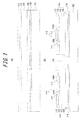
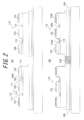
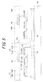
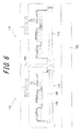
- FIG. 7 is a schematic side cross-sectional view illustrating a process subsequent to FIG. 6.
- FIGS. 1 and (B) are schematic top views of FIGS. 1 (B) and 2 (A), respectively.
- (A) and (B) are schematic top views of FIGS. 2 (B) and 3 (B), respectively.
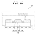
- FIG. 6 is a schematic side cross-sectional view of a group III nitride semiconductor light emitting device 200 according to another embodiment of the present invention.
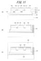
- FIGS. 4A to 4C are schematic side cross-sectional views showing a part of the steps of the method for manufacturing the group III nitride semiconductor light emitting device 300 according to another embodiment of the present invention.
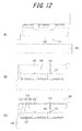
- (A)-(C) show the process following FIG.11 (C) with the typical side surface sectional drawing.
- (A) And (B) is a schematic top view of FIG. 11 (A) and FIG. 12 (C), respectively.
- (A) to (C) are SEM images of the surface of the i-type GaN layer in Examples 1, 3, and 4, respectively. It is a model side surface sectional view of the conventional group
- FIG. 8A is a top view corresponding to FIG. 1B, and the II cross section in FIG. 8A corresponds to FIG. Note that cross-sectional views other than FIG. 1B are also in the same position.
- FIG. 8B is a top view corresponding to FIG.
- FIG. 9A is a top view corresponding to FIG.
- FIG. 9B is a top view corresponding to FIG.
- a lift-off layer 104 is formed on a growth substrate 102.
- an i-type group III nitride semiconductor layer 106 (hereinafter referred to as “i-layer”) is formed as a buffer layer, and an n-type group III nitride semiconductor layer 108 which is the first conductivity type is formed.
- n layer a light emitting layer 110 and a second conductivity type p-type group III nitride semiconductor layer 112 (hereinafter referred to as “p layer”) are sequentially stacked.
- the i-type group III nitride semiconductor layer refers to a layer to which a specific impurity is not intentionally added (undoped layer). Ideally, it is preferable to use a semiconductor that does not contain impurities at all. However, a semiconductor that does not function electrically as p-type or n-type may be used, and has a low carrier concentration (for example, less than 5 ⁇ 10 16 / cm 3 Can be referred to as i-type.
- a part of the p layer 112, the light emitting layer 110, the n layer 108, and the i layer 106 is removed, so that a part of the growth substrate 102 is formed.
- the grooves 116 exposed at the bottom in a lattice shape, a plurality of semiconductor structure portions 114 each including an i layer 106, an n layer 108, a light emitting layer 110, and a p layer 112 having a quadrangular cross section are aligned.
- a structure formed on the growth substrate 102 and defined by the grooves 116 is hereinafter referred to as an element unit 115.
- the element unit 115 finally becomes each group III nitride semiconductor light emitting element.
- a substrate including the growth substrate 102 and all structures formed thereon is called a “wafer”.
- each element unit 115 a part of the p layer 112 and the light emitting layer 110 is removed to form a recess 117 in the semiconductor structure 114, and n A step of exposing a part of the layer 108 is performed.
- the exposed portion 108A of the n layer is circular, and a plurality (four locations) are formed in each semiconductor structure portion 114.
- the arrangement position, the number of arrangement, and the like can be appropriately set in consideration of the current spreading length and the chip size due to the layer structure of the semiconductor structure 114.
- each element unit 115 a circular n-side contact as a first contact layer on the exposed portion 108A of the n layer at the bottom of the recess 117.
- a step of forming a layer 118 and forming a p-side contact layer 120 as a second contact layer on almost the entire surface of the p layer 112 is performed.
- a step of forming an insulating layer 122 in each element unit 115 is performed.
- the insulating layer 122 is formed on the exposed surface of the element unit 115, specifically, on the exposed portion of the semiconductor structure 114, the n-side contact layer 118, and the p-side contact layer 120.
- the insulating layer 122 is not formed on a part of the n-side contact layer 118 and a part of the p-side contact layer 120 but is exposed.
- the exposed portion 118A of the n-side contact layer has a circular shape at the center portion of the n-type contact layer 118, and the exposed portion 120A of the p-type contact layer is p-type in the top view (FIG. 9A).
- the layer 112 extends in a straight line between the end portion 112A of the layer 112 and the exposed portion 108A of the n layer closest to the end portion.
- a portion where the exposed portion 108A of the n layer, the n-side contact layer 118, and the p-side contact layer 120 are covered with the insulating layer 122 is indicated by a broken line.
- the shape of the exposed portion 108A for forming the n-type contact layer is not necessarily circular, and may be concentric or comb-shaped.
- the lattice-shaped grooves 116 are closed with the first resin 124 every other row in the vertical direction. Accordingly, only one side surface of each element unit 115 is covered with the first resin 124. The first resin 124 is removed in a later step.
- a plating seed layer 126 is formed on almost the entire exposed surface on the front side of the wafer.
- plating is performed on the insulating layer 122 between the exposed portion 120A of the p-contact layer and the exposed portion 118A of the n-contact layer in a straight line substantially parallel to the exposed portion 120A of the p-contact layer.
- the seed layer 126 is not formed, and a part of the insulating layer 122 is exposed.
- each element unit 115 specifically, an exposed portion of the insulating layer 122 where the plating seed layer 126 is not formed is covered on a part of the insulating layer 122.
- a step of forming a first structure 128 made of an insulator and crossing the exposed surface of each element unit 115 is performed. Due to the first structure 128, the exposed surface of each element unit 115 includes a first exposed surface 130 having an exposed portion 118A of the n-side contact layer and a second exposed surface 132 having an exposed portion 120A of the p-side contact layer. Separated. The first and second exposed surfaces 130 and 132 are defined as exposed surfaces excluding the plating seed layer 126.
- the left side of the first structure 128 is the first exposed surface 130 and the right side is the second exposed surface 132.
- the second resin 134 is formed on the first resin 124 to the same height as the first structure 128 via the plating seed layer 126. This second resin 134 is also removed in a later step.
- the plating process includes a first plating process shown in FIGS. 3B and 9B, a second structure forming process shown in FIG. 4, and a second plating process shown in FIG. Including.
- a first layer 136A of the first support body is formed on the first exposed surface 130, and the second exposed surface 132 is formed.
- a first layer 138A of the second support body is grown by plating. The plating growth is stopped at the stage where the first layers 136A and 138A do not merge.
- the first layer 136A of the first support body is in contact with the exposed portion 118A (broken line in the figure) of the n-side contact layer, and the first layer 138A of the second support body is on the p side. It is in contact with the exposed portion 120A (broken line in the figure) of the contact layer.
- the first structure 128 is located between the first layers 136A and 138A of the first and second support bodies.
- a second structure 140 made of an insulator connected to the first structure 128 is formed on the first layer 136A of the first support body.
- the second structure 140 is formed linearly wider than the first structure 128.
- the third resin 142 connected to the second resin 134 is linearly formed on the second resin 134.
- the second layer 136B of the first support body and A second layer 138B of the second support body is further grown by plating.
- the plating growth is stopped at the stage where the second layers 136B and 138B do not merge.
- the second structure 140 is located between the second layers 136B and 138B of the first and second support bodies.
- the first support body 136 that functions as the n-side electrode as the first electrode is formed in contact with the exposed portion 118A of the n-side contact layer through the recess 117,
- a second support body 138 that functions as a p-side electrode that is a second electrode can be formed on the second exposed surface 132 in contact with the exposed portion 120A of the second contact layer.
- the second support body of the second support body is larger than the area of the first layer 138A of the second support body after the first plating process. The upper area of the two layers 138B increases.
- the growth substrate 102 is removed from the semiconductor structure 114 of each element unit 115 by supplying an etching solution to the gap 144 and removing the lift-off layer 104 using a chemical lift-off method. A peeling process is performed.
- the removal of the lift-off layer 104 proceeds in one direction (arrow direction in FIG. 6) from the side surface that is the gap 144.
- the growth substrate 102 may be peeled off from each element unit 115 by a laser lift-off method.
- the surface of the i layer 106 exposed by removing the lift-off layer 104 is further etched to form irregularities on the surface of the i layer 106.
- the present embodiment is characterized in that the i layer 106 remains as a light extraction surface instead of completely removing the i layer 106 and exposing the n layer 108. Furthermore, the 1st support body 136 and the 2nd support body 138 are cut
- a plurality of group III nitride semiconductor light emitting devices in which the semiconductor structure 114 is supported on the support 146 including the first and second support bodies 136 and 138 and the first and second structures 128 and 140. 100 can be made.
- an n-side electrode (first support body 136) that is a part of the support is formed on the p-layer 112 side of the semiconductor structure.
- Embodiment 2 Manufacturing method of group III nitride semiconductor light emitting device 200
- the manufacturing method of the group III nitride semiconductor light-emitting device 200 concerning other embodiment of this invention is demonstrated.
- This embodiment is the same as the method for manufacturing the element 100 except for the step of forming irregularities on the surface of the i layer 106.
- first unevenness corresponding to the shape of the mask is formed by dry etching using a mask (not shown), and then the first unevenness surface is formed on the surface of the first unevenness by wet etching with an alkaline solution. Second irregularities finer than the irregularities are formed.
- the surface of the i layer 106 thus obtained is schematically shown in FIG.
- Group III nitride semiconductor light emitting device 100 A group III nitride semiconductor light emitting device 100 will be described with reference to FIG.
- Group III nitride semiconductor light emitting device 100 includes a semiconductor structure 114 having an i layer 106, an n layer 108, a light emitting layer 110, and a p layer 112 in this order.
- An n-side contact layer 118 is provided on the n layer 108 at the bottom of the recess 117 penetrating the p layer 112 and the light emitting layer 110.
- a p-side contact layer 120 is provided on the p layer 112.
- an insulating layer 122 for insulating the n-side contact layer 118 and the p-side contact layer 120 includes a part of the n-side contact layer 118, a part of the p-side contact layer 120, and the n-side contact layer 118 and p It is provided on the semiconductor structure 114 located between the side contact layer 120.
- a structure comprising a single first support body 136, a single second support body 138, and an insulator positioned between adjacent first and second support bodies 136, 138. 128 and 140 are provided.
- the first support body 136 partially contacts the n-side contact layer 118 via the recess 117 and functions as an n-side electrode.
- the second support body 138 partially contacts the p-side contact layer 120 and functions as a p-side electrode.
- the first and second support bodies 136 and 138 and the structures 128 and 140 serve as a support body 146 that supports the semiconductor structure portion 114.
- i layer 106 serves as a light extraction surface. Concavities and convexities are formed on the surface of the i layer 106 to increase the light extraction efficiency.
- the semiconductor structure 114 has a plurality of recesses and the n-side contact layer 118 at a plurality of locations. For this reason, a current flows uniformly in the element, and the element characteristic (light emission output in the case of LED) is improved.
- the first and second support bodies 136 and 138 include first layers 136A and 138A provided on the insulating layer 120, and second layers 136B and 138B provided on the first layers 136A and 138A, respectively. including.
- the structures 128 and 140 are connected to the first structure 128 positioned between the first layers 136A and 138A of the first and second support bodies, and are connected to the first structure 128.
- a second structure 140 positioned between the second layers 136B and 138B.
- the upper area of the second layer 138B of the second support body is larger than the upper area of the first layer 138A of the second support body.
- This structure can be produced by the two-step plating described above.
- the first layer 138A of the second support body inevitably becomes considerably smaller than the first layer 136A of the first support body.
- the upper area of the second layer 138B of the second support body can be made larger than that of the first layer 138A of the second support body by the two-step plating. In this case, there is an effect that the alignment when the group III nitride semiconductor light emitting device 100 is mounted on a separate printed wiring board or the like becomes easy.
- the element 200 is the same as the element 100 except for the surface state of the i layer 106.
- the surface of the i layer 106 is a two-step uneven surface including a first unevenness and a second unevenness that is formed on the first uneven surface and is finer than the first unevenness. Thereby, the light extraction efficiency from the i layer 106 (light extraction surface) is further improved, and the light emission output is improved.
- FIG. 13A is a top view corresponding to FIG. 11A
- a II-II cross section in FIG. 13A corresponds to FIG.
- FIG. 13B is a top view corresponding to FIG. 12C
- a III-III cross section in FIG. 13B corresponds to FIG. 11 to 13, unlike the first embodiment, only one element unit is shown. Further, the description of the same steps as those in the first embodiment is omitted or simplified.
- a lift-off layer 104 is formed on a growth substrate 102, and an i layer 106, an n layer 108, a light emitting layer 110, and a p layer 112 are formed thereon. Are sequentially laminated. Subsequently, the trench 116 is formed to form the semiconductor structure 114. Subsequently, a step of removing a part of the p layer 112 and the light emitting layer 110 to form a recess 117 in the semiconductor structure 114 and exposing a part of the n layer 108 is performed.
- the n-side contact layer 118 is formed on the exposed portion 108 A of the n layer at the bottom of the recess 117, and the p-side contact layer 120 is formed on the p layer 112.
- the steps so far are the same as those in the first embodiment.
- the shape of the recess 117 that is, the shape of the n-side contact layer 118 is different from that of the first embodiment, and as shown in FIG.
- the recess 117 is filled with the insulator 150.
- the insulator 150 serves to insulate the n-side contact layer 118 and the p-side contact layer 120.
- the groove 116 is closed with the first resin 124.
- a plating seed layer 126 is formed on the front side exposed surface of the wafer.
- the second support body 138 is plated and grown from the plating seed layer 126.
- the lift-off layer 104 is removed using a chemical lift-off method by supplying an etchant from the gap formed by removing the first resin 124, as in the first embodiment.
- a lift-off process for peeling the growth substrate 102 from the semiconductor structure 114 is performed.
- the i layer 106 is exposed.
- the laser lift-off method may be used as in the first embodiment.
- FIG. 12B is drawn upside down from the previous drawings.
- a hole 152 communicating with the n-side contact layer 118 is formed in a part of the i layer 106 and the n layer 108 exposed by the lift-off process.
- an n-side electrode 154 that contacts the n-side contact layer 118 through the hole 152 is formed in the hole 152 and on the i layer 106. To do.
- a hole 152 and an n-side electrode 154 are formed at two opposing corner portions of the n-side contact layer 118 extending in a quadrangular ring shape.
- the i layer 106 remains as a light extraction surface and the unevenness is formed on the surface of the i layer 106. The same is true for the singulation process.
- the second support body 138 is in contact with the p-side contact layer 120 and functions as a p-side electrode, and also serves as a support for the semiconductor structure portion 114.
- This embodiment is common to Embodiments 1 and 2 in that the n-side contact layer 118 is formed from the p-layer 112 and the light-emitting layer 110 side, but the n-side electrode 154 is formed on the i-layer 106 side. Different from the first and second embodiments.
- the feature of the present invention common to the group III nitride semiconductor light emitting devices 100 to 300 is that, as described above, the i layer 106 remains as the light extraction surface. The reason is not clear, but forming the irregularities on the surface of the i layer 106 is more effective in improving the output than exposing the n layer 108 and forming the irregularities on the surface of the n layer 108. As a result, the present inventors have found that the light emission output can be improved as compared with the case where the n layer is exposed.
- the growth substrate 102 is preferably a sapphire substrate or an AlN template substrate in which an AlN film is formed on a sapphire substrate.
- the chemical lift-off method it may be appropriately selected depending on the type of lift-off layer to be formed, the composition of Al, Ga, and In of the group III nitride semiconductor layer, the quality of the LED chip, the cost, and the like.
- the lift-off layer 104 is preferable because a metal other than Group III such as CrN or a metal nitride buffer layer can be dissolved by chemical selective etching. It is preferable to form the film by sputtering, vacuum deposition, ion plating, or MOCVD. Usually, the thickness of the lift-off layer 104 is about 2 to 100 nm. This is not always necessary for laser lift-off.
- the i layer 106, the n layer 108, the light emitting layer 110, and the p layer 112 are made of an arbitrary group III nitride semiconductor such as GaN or AlGaN.
- the light emitting layer 110 has a multiple quantum well (MQW) structure of a group III nitride semiconductor.
- MQW multiple quantum well
- These layers can be epitaxially grown on the lift-off layer 104 by, for example, the MOCVD method.
- the first conductivity type is n-type
- the second conductivity type is p-type.
- the i layer 106 is preferably formed with a thickness of 3 to 10 ⁇ m, and more preferably with a thickness of 5 to 10 ⁇ m.
- the i layer 106 is preferably formed with a thickness of 3 to 10 ⁇ m, and more preferably with a thickness of 5 to 10 ⁇ m.
- the i layer 106 remaining after lift-off is preferably 1 to 9 ⁇ m in thickness, and more preferably 3 to 9 ⁇ m in order to form a two-step unevenness.
- the thickness of the n layer 108 can be 1 to 9 ⁇ m immediately below the light emitting layer 110, but it is preferable to make it as thin as possible within this range.
- immediately under the light emitting layer 110 is preferably 10 to 90%. This is because, as described above, the crystallinity of the n layer can be improved by making the i layer thick and the n layer thin.
- the thickness of the i layer with unevenness is defined by (maximum thickness of convex vertex + minimum thickness of concave bottom) / 2 when an uneven surface is observed.
- the thickness of the light emitting layer 110 and the p layer 112 is typically 1 to 100 nm and 10 to 1000 nm, respectively.
- the cross-sectional shape of the semiconductor structure 114 is not particularly limited as long as it is substantially rectangular, but is preferably rectangular from the viewpoint of effective area.
- This substantially quadrilateral includes, for example, a quadrilateral having a slightly rounded or chamfered corner.
- the cross-sectional shape based on polygons, such as a rectangle and a hexagon in which the length of a short side and a long side differs, may be sufficient.
- One side of the semiconductor structure 114 is usually 250 to 3000 ⁇ m.
- the maximum width of the groove 116 is preferably in the range of 40 to 200 ⁇ m, and more preferably in the range of 60 to 100 ⁇ m. This is because when the thickness is 40 ⁇ m or more, the etching solution can be sufficiently smoothly supplied to the groove 116, and when the thickness is 200 ⁇ m or less, the loss of the light emitting area can be minimized.
- the step of removing a part of the p layer 112 and the light emitting layer 110 and exposing a part of the n layer 108 is preferably performed by a dry etching method using a resist as a mask. This is because the etching end point of the n layer 108 can be controlled with good reproducibility.
- the n-side contact layer 118 is formed by a lift-off method using a resist as a mask.
- a resist As the electrode material, Al, Cr, Ti, Ni, Ag, Au, or the like is used.
- the p-side contact layer 120 is formed by a lift-off method using a resist as a mask. Ni, Ag, Ti, Pd, Cu, Au, Rh, Ru, Pt, Ir, etc. are used as the electrode material.
- the insulating film 122 is made of, for example, SiO 2 or SiN, and is formed by wet etching or dry etching using a resist pattern as a mask after forming a film of 0.5 to 2.0 ⁇ m by PECVD.
- a permanent film photoresist (such as SU-8) used in SiO 2 , SiN, MEMS, or the like, or a resin such as insulating epoxy or polyimide is used.
- the first resin 124 may be formed by applying an arbitrary resist material and using an arbitrary patterning technique. The same applies to the second resin 134 and the third resin 142.
- the first structure 128 and the second structure 140 are part of the element as a support.
- an insulating material for example, a resin such as epoxy resin or polyimide, or an inorganic material such as SiO 2 or SiN can be used. Any patterning technique may be used, but the process can be simplified if it is a permanent film photoresist (such as SU-8) used in MEMS (Micro Electro Mechanical System) or the like.
- the height is desirably 10 to 100 ⁇ m, and the width is desirably 10 to 100 ⁇ m and 500 to 900 ⁇ m, respectively.
- the first support body 136 and the second support body 138 can be formed by a plating method such as wet plating or dry plating.
- a plating method such as wet plating or dry plating.
- Cu, Ni, Au or the like can be used as the surface of the plating seed layer 126 (conductive support body side).
- the plating seed layer 126 can be formed by sputtering, for example.
- the plating seed layer 126 may have a thickness of 2.0 to 20 ⁇ m, and the first support body 136 and the second support body 138 may have a thickness of about 10 to 200 ⁇ m.
- the first resin 124, the second resin 134, and the third resin 142 can be performed using a solution that dissolves a resin such as acetone or alcohol.
- a resin such as acetone or alcohol.
- the plating seed layer 126 between the first resin 124 and the second resin 134 is not dissolved in acetone or the like, but the plating seed layer 126 is a very thin film compared to the first resin 124 and the second resin 134. Therefore, removal is easy. It may be removed mechanically or by metal etching or the like. At this time, the first structure 128 and the second structure 140 are not removed.
- the removal of the lift-off layer 104 is performed by a general chemical lift-off method or a photochemical lift-off method.
- the chemical lift-off method is a method of etching a lift-off layer.
- a method of performing etching while activating the lift-off layer by irradiating light such as ultraviolet light during etching is called a photochemical lift-off method.
- Etching solutions that can be used include known ceric ammonium nitrate solutions and ferricyanic potassium-based solutions when the lift-off layer is CrN, and selective etching methods such as hydrochloric acid, nitric acid, and organic acids when the lift-off layer is ScN.
- a liquid can be mentioned.
- the growth substrate can also be removed by a laser lift-off method or a dissolution / mechanical polishing removal method of the growth substrate itself.
- the surface of the i layer 106 exposed by removing the lift-off layer 104 is preferably cleaned by wet cleaning.
- the dry etching for forming the first unevenness is, for example, reactive ion etching (RIE), which is isotropic etching.
- RIE reactive ion etching
- gases such as chlorine, silicon tetrachloride, and boron chloride can be used.
- the resist is used as a mask to form by dry etching.
- the first concavo-convex portion can have a convex dimension of 1 to 10 ⁇ m in length and width, a concave width of 1 to 10 ⁇ m, and a depth of approximately 1 to 10 ⁇ m.
- the wet etching for forming the second unevenness can be performed with an alkaline solution such as a 2.38 mass% tetramethylammonium hydroxide (TMAH) solution, an NaOH solution, or a KOH solution, for example.
- TMAH tetramethylammonium hydroxide
- the second unevenness has a polygonal pyramid shape (for example, a hexagonal pyramid or a hexagonal pyramid deformation (rounded corners, etc.)), and the height (depth) of the cross section can be 2.5 ⁇ m or less.
- the hole 152 is formed by a dry etching method using a resist as a mask.
- the n-side electrode 154 is formed by a lift-off method after vapor-depositing an electrode material by an EB vapor deposition method or a sputtering method.
- a blade dicer or a laser dicer can be used for the cutting of the first support body 136 and the second support body 138.
- Example 1A to 3B were performed, and then an LED chip was manufactured by a chemical lift-off method without performing two-step plating. Specifically, first, as shown in FIG. 1A, a lift-off layer (CrN layer, thickness: 18 nm) is formed by forming a Cr layer on a sapphire substrate by sputtering and performing heat treatment in an atmosphere containing ammonia.
- a lift-off layer CrN layer, thickness: 18 nm
- An i-type GaN layer (thickness: 7.0 ⁇ m), an n-type GaN layer (thickness: 3.0 ⁇ m), a light emitting layer (AlInGaN-based MQW layer, thickness: 0.1 ⁇ m), p-type GaN Layers (thickness: 0.2 ⁇ m) were sequentially epitaxially grown by MOCVD.
- a part of the p-type GaN layer, the light emitting layer, the n-type GaN layer, and the i-type GaN layer is removed by dry etching to form lattice-shaped grooves.
- a plurality of semiconductor structure portions having a transverse cross-sectional shape aligned in the vertical and horizontal directions were formed.
- One side of the semiconductor structure was 1500 ⁇ m, and the maximum width of the groove was 100 ⁇ m.
- the photoresist as a mask, a part of the p-type GaN layer and the light emitting layer was removed by ICP-RIE dry etching to expose a part of the n-type GaN layer.
- the exposed portion of the n-type GaN layer is arranged at four locations in each element unit, but in this embodiment, it is 16 locations and the diameter is 60 ⁇ m.
- a circular n-side contact layer (on the exposed portion of the n-type GaN layer) is formed by EB evaporation.
- a p-side contact layer material: Ni / Ag / Ni / Ti, thickness: 5 mm / 200 nm / 25 mm / 25 ⁇
- a photoresist was formed and the photoresist was removed along with the deposited metal on the photoresist.
- the resist is used as a mask by BHF.
- Part of the insulating layer was wet etched to expose part of the n-side contact layer and part of the p-side contact layer.
- the photoresist was removed.
- the exposed portion of the n-side contact layer had a diameter of 30 ⁇ m
- the exposed portion of the p-side contact layer had a width of 60 ⁇ m.
- the lattice-like grooves were filled with photoresist (width: 100 ⁇ m, height: 10 ⁇ m) every other column in the vertical direction.
- a plating seed layer (Ti / Ni / Au, each thickness: 0.02 ⁇ m / 0.2 ⁇ m / 0. 6 ⁇ m) was formed.
- the insulating layer was exposed only at the position shown in FIG. 3A by wet etching using the photoresist as a mask.
- the exposed portion of the insulating layer had a width of 50 ⁇ m.
- the plating seed layer was divided into a region for forming a first support body, which will be described later, and a region for forming a second support body, which were electrically separated.
- the 1st structure (width: 100 micrometers, height: 30 micrometers) which consists of SU-8 was formed so that the exposed part of an insulating layer might be covered using the photolithographic method.
- a photoresist (width: 550 ⁇ m, height: 30 ⁇ m) was further formed on the photoresist formed in every other row in the groove, and the height was made the same as that of the first structure.
- Cu is formed from the plating seed layer by plating, and the first layer of the first and second support bodies (on the p-type GaN layer) (Thickness: 40 ⁇ m) was formed.
- the plating was electroplating using a copper sulfate electrolyte, the temperature of the solution was in the range of 25 to 30 ° C., and the film formation rate was 35 ⁇ m / hr.
- the widths of the first layers of the first and second support bodies were 1200 ⁇ m and 150 ⁇ m, respectively.
- the first support body and the second support body are electrically separated by the first structure.
- the selective etching solution for the lift-off layer was supplied to the gap, and the lift-off layer was removed by a chemical lift-off method, whereby the sapphire substrate was peeled from each element unit.
- the i-type GaN layer exposed by removing the lift-off layer is etched by about 2 ⁇ m by ICP-RIE dry etching, and further etched at 60 ° C. for 10 minutes using a 6 mol / L KOH solution. Further, about 2 ⁇ m was etched.
- the i-type GaN layer was etched by about 4 ⁇ m, and the thickness of the i-type GaN layer remaining after lift-off was 3.0 ⁇ m.
- a cross section of the surface of the i-type GaN layer was observed using an electron microscope (SEM), irregularities having an average depth of 0.5 ⁇ m were formed on the surface of the i-type GaN layer.
- FIG. 14A shows an SEM image of the surface of the i-type GaN layer. And the 1st support body and the 2nd support body were cut
- Example 2 An LED chip was manufactured by the method shown in FIGS. Specifically, a lift-off layer (CrN layer, thickness: 18 nm) is first formed on a sapphire substrate by sputtering to form a Cr layer and heat-treating in an atmosphere containing ammonia, and then an i-type GaN layer ( Thickness: 7.0 ⁇ m), n-type GaN layer (thickness: 3.0 ⁇ m), light emitting layer (AlInGaN-based MQW layer, thickness: 0.1 ⁇ m), p-type GaN layer (thickness: 0.2 ⁇ m) Sequentially epitaxial growth was performed by MOCVD.
- a lift-off layer CrN layer, thickness: 18 nm
- a part of the p-type GaN layer, the light-emitting layer, the n-type GaN layer, and the i-type GaN layer is removed by dry etching to form a lattice-shaped groove, whereby a plurality of cross-sectional shapes arranged in a vertical and horizontal manner with a square shape
- a number of semiconductor structures were formed.
- One side of the semiconductor structure was 1500 ⁇ m, and the maximum width of the groove was 100 ⁇ m.
- n-side contact layer material: Cr / Ni / Ag
- the photoresist is deposited metal on the photoresist. And removed.
- the recess was filled with an insulator (material: SU-8), and the n-side contact layer was enclosed. Further, using a photolithographic method, the lattice-like grooves were closed with photoresist (width: 100 to 140 ⁇ m, height: 10 to 20 ⁇ m) every other column in the vertical direction. Further, a plating seed layer (Ti / Ni / Au, each thickness: 0.02 ⁇ m / 0.2 ⁇ m / 0.6 ⁇ m) was formed on the exposed surface of the wafer by sputtering.
- a plating seed layer Ti / Ni / Au, each thickness: 0.02 ⁇ m / 0.2 ⁇ m / 0.6 ⁇ m
- Example 2 Cu was plated and grown from the plating seed layer under the same conditions as in Example 1 to form a second support body (thickness on the p-type GaN layer: 200 ⁇ m). Further, the photoresist provided in the groove was removed by the same method as in Example 1, the sapphire substrate was peeled off by the chemical lift-off method, and the exposed i-type GaN layer was etched.
- a hole communicating with the n-side contact layer was formed in a part of the i-type GaN layer and the n-type GaN layer by ICP-RIE dry etching. Holes were formed at two locations indicated by broken lines in FIG.
- n-side contact layer is made through the hole by lift-off method in which the photoresist is removed together with the deposited metal on the photoresist.
- An n-side electrode was formed in the hole and on the i-type GaN layer.
- the dimension (including the hole) of the n-side electrode on the i-type GaN layer was 100 ⁇ 100 ⁇ m.
- the 2nd support body was cut
- the thickness of the i-type GaN layer formed by epitaxial growth is 4.0 ⁇ m
- the thickness of the n-type GaN layer is 6.0 ⁇ m
- all the i-type GaN layer exposed by removing the lift-off layer is removed
- the n-type GaN layer 600 LED chips according to Comparative Example 1 were obtained in the same manner as in Example 1 except that the light extraction surface was exposed.
- irregularities having an average depth of 0.5 ⁇ m were formed on the surface of the n-type GaN layer.
- Example 3 After removing the lift-off layer and before wet etching, 600 LEDs according to Example 3 were used in the same manner as in Example 1 except that the i-type GaN layer was subjected to ICP-RIE etching using a resist mask. I got a chip.
- irregularities having a convex portion size of 2 ⁇ m in length and width, a concave portion width of 2 ⁇ m, and a depth of 1 ⁇ m are formed, and the irregular surface has an average depth of 0.5 ⁇ m. Was formed.
- FIG. 14B shows an SEM image of the surface of the i-type GaN layer.
- Example 4 Except for the ICP-RIE etching time of 600 seconds, 600 LED chips according to Example 4 were obtained in the same manner as in Example 3. On the surface of the i-type GaN layer, irregularities having a convex portion size of 2 ⁇ m in length and width, a concave portion width of 2 ⁇ m, and a depth of 2 ⁇ m are formed, and the irregular surface has an average depth of 0.5 ⁇ m. Was formed.
- FIG. 14C shows an SEM image of the i-type GaN layer surface.
- Examples 1 and 2 were able to improve the light emission output Po while maintaining the forward voltage Vf as compared with Comparative Example 1. Further, in Examples 3 and 4 in which the two-step uneven surface was formed, the light emission output Po could be further improved by 5% and 10%, respectively, as compared with Example 1.
Landscapes
- Led Devices (AREA)
Description
本発明は、III族窒化物半導体発光素子およびその製造方法に関する。
半導体素子には、電界効果トランジスタ(FET)、発光ダイオード(LED)などの各種デバイスがある。これらには、例えば、III族元素とV族元素との化合物からなるIII−V族半導体が用いられる。
III族元素としてAl,Ga,Inなどを用い、V族元素としてNを用いたIII族窒化物半導体は、高融点で窒素の解離圧が高くバルク単結晶成長が困難であり、大口径で安価な導電性単結晶基板が無いという理由から、サファイア基板上に成長させることにより形成するのが一般的である。
しかしながら、サファイア基板は絶縁性であって電流が流れない。そのため近年、サファイア基板などの成長用基板上に、発光層を含むIII族窒化物半導体層を形成し、このIII族窒化物半導体層上に、別途支持体を貼合せた後、サファイア基板を剥離(リフトオフ)して、III族窒化物半導体層が支持体に支持された縦型構造のLEDチップなどを作製する方法が研究されている。
この方法で作製されるLEDチップの一態様として、図15に示す構造が知られている。図14のIII族窒化物半導体LEDチップ400は、n型III族窒化物半導体層(n層)401、発光層402およびp型III族窒化物半導体層(p層)403をこの順に有する半導体構造部404が、サブマウント基板410に支持された構造を有する。p層403および発光層402を貫通する凹部の底のn層401上にn側コンタクト層405が設けられ、p層403上にはp側コンタクト層406が設けられる。そして、n側コンタクト層405とp側コンタクト層406とを絶縁する絶縁層407が、両者の間に形成されている。n側コンタクト層と導通するAuバンプ408Aとp側コンタクト層と導通するAuバンプ408Bとが、ともに半導体構造部404の同じ側に延びている。サブマウント基板410には、n層用配線410Aおよびp層用配線410Bが設けられている。そして、Auバンプ408Aとn層用配線410Aとが接合し、Auバンプ408Bとp層用配線410Bとが接合する。Auバンプ408A,408Bの間は、エポキシ樹脂からなるアンダーフィル409が充填されている。支持体410の裏面にはn層用配線410Aおよびp層用配線410Bと導通するハンダ411が設けられ、LEDチップ400は、このハンダ411を介してパッケージ基材やプリント配線板(図示せず)などに実装される。LEDチップ400では、n層201の表面が光取り出し面となる。
このようなLEDチップ400は、例えば以下のようなリフトオフ法により製造される。まず、サファイア基板などの成長用基板(図示せず)上に、n層401、発光層402、p層403をエピタキシャル成長させる。その後、エッチング、蒸着、メッキ、パターニングなどの公知の成膜技術を用いて、n側コンタクト層405、p側コンタクト層406、絶縁層407、Auバンプ408A,408Bを形成する。その後、Auバンプ408Aとn層用配線410Aとが接合し、Auバンプ408Bとp層用配線410Bとが接合するように、支持体410に対して成長用基板を位置あわせして押しつける。その後、アンダーフィル409を注入し、最後に、成長用基板をリフトオフして、LEDチップ400を得る。このような製造方法は、特許文献1および特許文献2に記載されている。
サファイア基板上にバッファ層としてi型III族窒化物半導体層(i層、図示せず)を形成してから、n層401、発光層402、p層403をエピタキシャル成長させることもある。
従来、バッファ層としてi層を形成する場合でも、i層は基本的に必要最小限の厚み(例えば2μm程度)で形成し、リフトオフ後に露出したi層は除去して、n層を露出させ、n層表面を光取り出し面としていた。後に除去しなければならないi層を厚くエピ成長することは無駄であると考えられていた。しかしながら、本発明者らの検討によれば、このような従来のLEDチップには発光出力に改善の余地があることが判明した。
そこで本発明は、上記課題に鑑み、発光出力を向上させたIII族窒化物半導体発光素子およびその製造方法を提供することを目的とする。
上記目的を達成するため、本発明の要旨構成は以下のとおりである。
(1)i型III族窒化物半導体層、第1導電型III族窒化物半導体層、発光層および第2導電型III族窒化物半導体層をこの順に有する半導体構造部と、
前記第2導電型III族窒化物半導体層および前記発光層を貫通する凹部の底で前記第1導電型III族窒化物半導体層上に設けられた第1コンタクト層と、
前記第2導電型III族窒化物半導体層上に設けられた第2コンタクト層と、
前記半導体構造部の前記第2導電型III族窒化物半導体層側に設けられ、前記第2コンタクト層と接触して第2電極として機能するとともに、支持体の少なくとも一部となる第2サポート体と、
前記半導体構造部の前記第2導電型III族窒化物半導体層側、または、前記i型III族窒化物半導体層上に設けられた、前記第1コンタクト層と電気的に接続する第1電極と、
を有し、前記i型III族窒化物半導体層が光取り出し面となることを特徴とするIII族窒化物半導体発光素子。
(1)i型III族窒化物半導体層、第1導電型III族窒化物半導体層、発光層および第2導電型III族窒化物半導体層をこの順に有する半導体構造部と、
前記第2導電型III族窒化物半導体層および前記発光層を貫通する凹部の底で前記第1導電型III族窒化物半導体層上に設けられた第1コンタクト層と、
前記第2導電型III族窒化物半導体層上に設けられた第2コンタクト層と、
前記半導体構造部の前記第2導電型III族窒化物半導体層側に設けられ、前記第2コンタクト層と接触して第2電極として機能するとともに、支持体の少なくとも一部となる第2サポート体と、
前記半導体構造部の前記第2導電型III族窒化物半導体層側、または、前記i型III族窒化物半導体層上に設けられた、前記第1コンタクト層と電気的に接続する第1電極と、
を有し、前記i型III族窒化物半導体層が光取り出し面となることを特徴とするIII族窒化物半導体発光素子。
(2)前記第1電極は、前記半導体構造部の前記第2導電型III族窒化物半導体層側に設けられ、前記凹部を介して前記第1コンタクト層と接触するとともに、前記支持体の一部となる第1サポート体である上記(1)に記載のIII族窒化物半導体発光素子。
(3)前記第1電極は、前記i型III族窒化物半導体層および前記第1導電型III族窒化物半導体層の一部に形成された、前記第1コンタクト層へと連通する穴と、前記i型III族窒化物半導体層上とに設けられている上記(1)に記載のIII族窒化物半導体発光素子。
(4)前記i型III族窒化物半導体層の表面が凹凸を有する上記(1)~(3)のいずれか1項に記載のIII族窒化物半導体発光素子。
(5)前記i型III族窒化物半導体層の表面が、第1の凹凸と、該第1の凹凸表面に形成された、前記第1の凹凸よりも微細な第2の凹凸とを含む2段階凹凸表面である上記(4)に記載のIII族窒化物半導体発光素子。
(6)成鳥用基板の上に、i型III族窒化物半導体層、第1導電型III族窒化物半導体層、発光層および第2導電型III族窒化物半導体層を順次積層してなる半導体構造部を形成する工程と、
前記第2導電型III族窒化物半導体層および前記発光層の一部を除去して、前記半導体構造部に凹部を形成し、前記第1導電型III族窒化物半導体層の一部を露出させる工程と、
前記凹部の底の前記第1導電型III族窒化物半導体層の露出部の上に第1コンタクト層を形成し、前記第2導電型III族窒化物半導体層上に第2コンタクト層を形成する工程と、
前記半導体構造部の前記第2導電型III族窒化物半導体層側に、前記第2コンタクト層と接触して第2電極として機能するとともに、支持体の少なくとも一部となる第2サポート体を形成する工程と、
リフトオフ法を用いて前記成長用基板を前記半導体構造部から剥離するリフトオフ工程と、
前記半導体構造部の前記第2導電型III族窒化物半導体層側、または、前記リフトオフ工程により露出した前記i型III族窒化物半導体層上に、前記第1コンタクト層と電気的に接続する第1電極を形成する工程と、
を有し、露出した前記i型III族窒化物半導体層を光取り出し面として残存させることを特徴とするIII族窒化物半導体発光素子の製造方法。
前記第2導電型III族窒化物半導体層および前記発光層の一部を除去して、前記半導体構造部に凹部を形成し、前記第1導電型III族窒化物半導体層の一部を露出させる工程と、
前記凹部の底の前記第1導電型III族窒化物半導体層の露出部の上に第1コンタクト層を形成し、前記第2導電型III族窒化物半導体層上に第2コンタクト層を形成する工程と、
前記半導体構造部の前記第2導電型III族窒化物半導体層側に、前記第2コンタクト層と接触して第2電極として機能するとともに、支持体の少なくとも一部となる第2サポート体を形成する工程と、
リフトオフ法を用いて前記成長用基板を前記半導体構造部から剥離するリフトオフ工程と、
前記半導体構造部の前記第2導電型III族窒化物半導体層側、または、前記リフトオフ工程により露出した前記i型III族窒化物半導体層上に、前記第1コンタクト層と電気的に接続する第1電極を形成する工程と、
を有し、露出した前記i型III族窒化物半導体層を光取り出し面として残存させることを特徴とするIII族窒化物半導体発光素子の製造方法。
(7)前記第1電極を形成する工程は、前記半導体構造部の前記第2導電型III族窒化物半導体層側に、前記凹部を介して前記第1コンタクト層と接触するとともに、前記支持体の一部となる前記第1電極としての第1サポート体を形成する工程を含む上記(6)に記載のIII族窒化物半導体発光素子の製造方法。
(8)前記第1電極を形成する工程は、前記リフトオフ工程により露出した前記i型III族窒化物半導体層および前記第1導電型III族窒化物半導体層の一部に、前記第1コンタクト層へと連通する穴を形成する工程と、前記穴を介して前記第1コンタクト層と接触する前記第1電極を前記穴および前記i型III族窒化物半導体層上に形成する工程と、を含む上記(6)に記載のIII族窒化物半導体発光素子の製造方法。
(9)露出した前記i型III族窒化物半導体層に対してエッチング処理を施し凹凸を形成する工程をさらに有する上記(6)~(8)のいずれか1項に記載のIII族窒化物半導体発光素子の製造方法。
(10)前記凹凸を形成する工程は、マスクを用いたドライエッチングにより前記マスクの形状に対応した第1の凹凸を形成する工程と、アルカリ溶液によるウェットエッチングにより前記第1の凹凸表面に前記第1の凹凸よりも微細な第2の凹凸を形成する工程と、を含む上記(9)に記載のIII族窒化物半導体発光素子の製造方法。
本発明によれば、発光出力を向上させたIII族窒化物半導体発光素子およびその製造方法を提供することができる。
以下、図面を参照しつつ本発明の実施形態を説明する。
(実施形態1:III族窒化物半導体発光素子100の製造方法)
まず、図1~図9を参照して、本発明の一実施形態にかかるIII族窒化物半導体発光素子100の製造方法を、ケミカルリフトオフ法を用いた場合を例として説明する。まず、図1~図7の断面図と図8,9の上面図との対応関係を先に説明する。図8(A)は図1(B)に対応する上面図であり、図8(A)のI−I断面が図1(B)に対応する。なお、図1(B)以外の断面図も同様の位置でのものである。図8(B)は図2(A)に対応する上面図である。図9(A)は図2(B)に対応する上面図である。図9(B)は図3(B)に対応する上面図である。
まず、図1~図9を参照して、本発明の一実施形態にかかるIII族窒化物半導体発光素子100の製造方法を、ケミカルリフトオフ法を用いた場合を例として説明する。まず、図1~図7の断面図と図8,9の上面図との対応関係を先に説明する。図8(A)は図1(B)に対応する上面図であり、図8(A)のI−I断面が図1(B)に対応する。なお、図1(B)以外の断面図も同様の位置でのものである。図8(B)は図2(A)に対応する上面図である。図9(A)は図2(B)に対応する上面図である。図9(B)は図3(B)に対応する上面図である。
まず、図1(A)に示すように、成長用基板102の上にリフトオフ層104を形成する。リフトオフ層104の上に、バッファ層としてi型III族窒化物半導体層106(以後、「i層」という。)を形成し、さらに、第1導電型であるn型III族窒化物半導体層108(以後、「n層」という。)、発光層110および第2導電型であるp型III族窒化物半導体層112(以後、「p層」という。)を順次積層させる。なお、i型III族窒化物半導体層とは、特定の不純物を意図的に添加していない層(アンドープ層)のことをいう。理想的には不純物を全く含まない半導体とするのが好ましいが、電気的にp型またはn型として機能しない半導体とすればよく、キャリア濃度が小さいもの(例えば5×10¹⁶/cm3未満のもの)をi型と称することができる。
次に、図1(B)および図8(A)に示すように、p層112、発光層110、n層108およびi層106の一部を除去して、成長用基板102の一部が底部で露出する溝116を格子状に形成することで、横断面形状が四角形の縦横に整列したi層106、n層108、発光層110およびp層112からなる半導体構造部114を複数個形成する。成長用基板102上に形成され、溝116により区画される構造体を、以後、素子単位115と呼称する。素子単位115が最終的にそれぞれのIII族窒化物半導体発光素子となる。また、成長用基板102とこの上に形成される全ての構造物を含めたものは「ウェハ」と呼ぶ。
引き続き図1(B)および図8(A)に示すように、各素子単位115において、p層112および発光層110の一部を除去して、半導体構造部114に凹部117を形成し、n層108の一部を露出させる工程を行う。本実施形態では、n層の露出部108Aは円形で、各半導体構造部114中に複数(4箇所)形成される。ただし、半導体構造部114の層構成による電流の広がり長(Current Spreading Length)およびチップサイズを考慮して、配置位置や配置個数などは適宜設定することができる。
次に、図2(A)および図8(B)に示すように、各素子単位115において、凹部117の底のn層の露出部108Aの上に第1コンタクト層としての円形のn側コンタクト層118を形成し、p層112のほぼ全面の上に第2コンタクト層としてのp側コンタクト層120を形成する工程を行う。
次に、図2(B)および図9(A)に示すように、各素子単位115において、絶縁層122を形成する工程を行う。絶縁層122は、素子単位115の露出表面上、具体的には半導体構造部114の露出している部位、n側コンタクト層118の上、およびp側コンタクト層120の上に形成される。ただし、これらの図中にも示すように、n側コンタクト層118の一部およびp側コンタクト層120の一部には絶縁層122を形成せず、露出させる。本実施形態では、n側コンタクト層の露出部118Aは、n型コンタクト層118の中心部分で円形をなし、p型コンタクト層の露出部120Aは、上面図(図9(A))において、p層112の端部112Aと該端部から最も近いn層の露出部108Aとの間で直線状に延在する。図9(A)では、n層の露出部108A、n側コンタクト層118およびp側コンタクト層120が絶縁層122で覆われている部分を破線で示している。なお、n型コンタクト層形成のための露出部108Aの形状は円形でなくともよく、同心状、櫛形状などであっても良い、
引き続き図2(B)および図9(A)に示すように、格子状の溝116を縦方向に1列おきに第1樹脂124で塞ぐ。これにより、各素子単位115において1つの側面のみが第1樹脂124に覆われる。なお、この第1樹脂124は後の工程で除去される。
次に、図3(A)に示すように、ウェハの表側露出表面のほぼ全面にメッキシード層126を形成する。このとき、各素子単位115において、pコンタクト層の露出部120Aとnコンタクト層の露出部118Aとの間の絶縁層122上に、pコンタクト層の露出部120Aとほぼ平行な直線状に、メッキシード層126を形成せず、絶縁層122の一部を露出させる。
引き続き図3(A)に示すように、各素子単位115において、絶縁層122の一部の上に、具体的には、メッキシード層126の形成されていない絶縁層122の露出部を覆うように、絶縁体からなり各素子単位115の露出表面を横断する第1構造物128を形成する工程を行う。この第1構造物128により、各素子単位115の露出表面は、n側コンタクト層の露出部118Aがある第1露出表面130と、p側コンタクト層の露出部120Aがある第2露出表面132とに分離される。なお、第1および第2の露出表面130,132はメッキシード層126を除いた露出表面と定義する。図3(A)では、各素子単位115において第1構造物128の左側が第1露出表面130、右側が第2露出表面132となる。
引き続き図3(A)に示すように、第1樹脂124の上に、メッキシード層126を介して第2樹脂134を第1構造物128と同じ高さまで形成する。この第2樹脂134も後の工程で除去される。
次に、第1および第2露出表面130,132からそれぞれメッキ層を成長させるメッキ工程を行う。本実施形態では、メッキ工程は、図3(B)および図9(B)に示す第1メッキ工程と、図4に示す第2構造物形成工程と、図5に示す第2メッキ工程とを含む。
まず、第1メッキ工程では、図3(B)および図9(B)に示すように、第1露出表面130上に、第1サポート体の第1層136Aを形成し、第2露出表面132上に、第2サポート体の第1層138Aをメッキ成長させる。メッキ成長は、第1層136A,138A同士が合体しない段階で止める。図9(B)に示すように、第1サポート体の第1層136Aは、n側コンタクト層の露出部118A(図中破線)と接触し、第2サポート体の第1層138Aはp側コンタクト層の露出部120A(図中破線)と接触している。第1構造物128は、第1および第2サポート体の第1層136A,138Aの間に位置する。
続いて、図4に示すように、第1サポート体の第1層136Aの上に、第1構造物128と連結した、絶縁体からなる第2構造物140を形成する。本実施形態では、第1構造物128よりも幅広に第2構造物140を直線状に形成する。合わせて、第2樹脂134上に、これと連結した第3樹脂142を直線状に形成する。
続いて、第2メッキ工程では、図5に示すように、露出した第1サポート体の第1層136Aおよび第2サポート体の第1層138Aから、それぞれ第1サポート体の第2層136Bおよび第2サポート体の第2層138Bをさらにメッキ成長させる。メッキ成長は、第2層136B,138B同士が合体しない段階で止める。第2構造物140は、第1および第2サポート体の第2層136B,138Bの間に位置する。
このようにして、第1露出表面130上に、凹部117を介してn側コンタクト層の露出部118Aと接触して第1電極であるn側電極として機能する第1サポート体136を形成し、第2露出表面132上に、第2コンタクト層の露出部120Aと接触して第2電極であるp側電極として機能する第2サポート体138を形成することができる。このとき、図5から明らかなように、第2構造物140の配置に起因して、第1メッキ工程後の第2サポート体の第1層138Aの上面積よりも、第2サポート体の第2層138Bの上面積が大きくなる。
引き続き図5に示すように、第1樹脂124、第2樹脂134および第3樹脂142を除去することにより、成長用基板102および各素子単位115のリフトオフ層104に連通する空隙144を形成する。
次に、図6に示すように、空隙144にエッチング液を供給して、ケミカルリフトオフ法を用いてリフトオフ層104を除去することで、成長用基板102を各素子単位115の半導体構造部114から剥離する工程を行う。本実施形態では、各素子単位115では4つの側面のうち1つの側面のみが空隙144となっている。そのため、リフトオフ層104の除去は、空隙144となっている側面から一方向(図6中矢印方向)に進行する。レーザーリフトオフ法により成長用基板102を各素子単位115から剥離する方法でもよい。
最後に、図7に示すように、リフトオフ層104の除去によって露出したi層106表面をさらにエッチングし、i層106表面に凹凸を形成する。本実施形態では、i層106を完全に除去してn層108を露出させるのではなく、i層106を光取り出し面として残存させる点が特徴である。さらに、第1サポート体136および第2サポート体138を切断し、各素子単位115を個片化する。図7中の破線が切断箇所となる。
このようにして、第1および第2サポート体136,138ならびに第1および第2構造物128,140を含む支持体146に半導体構造部114が支持された複数個のIII族窒化物半導体発光素子100を作製することができる。本実施形態は、支持体の一部となるn側電極(第1サポート体136)を半導体構造部のp層112側に形成するタイプである。
(実施形態2:III族窒化物半導体発光素子200の製造方法)
図10を参照して、本発明の他の実施形態にかかるIII族窒化物半導体発光素子200の製造方法を説明する。本実施形態は、i層106表面に凹凸を形成する工程以外は、上記の素子100の製造方法と同じである。
図10を参照して、本発明の他の実施形態にかかるIII族窒化物半導体発光素子200の製造方法を説明する。本実施形態は、i層106表面に凹凸を形成する工程以外は、上記の素子100の製造方法と同じである。
本実施形態では、まず、マスク(図示せず)を用いたドライエッチングによりこのマスクの形状に対応した第1の凹凸を形成し、その後、アルカリ溶液によるウェットエッチングにより第1の凹凸表面に第1の凹凸よりも微細な第2の凹凸を形成する。このようにして得られたi層106の表面を模式的に図10に示す。
(III族窒化物半導体発光素子100)
図7を参照して、III族窒化物半導体発光素子100を説明する。III族窒化物半導体発光素子100は、i層106、n層108、発光層110およびp層112をこの順に有する半導体構造部114を含む。p層112および発光層110を貫通する凹部117の底にはn層108上にn側コンタクト層118が設けられている。また、p層112上にはp側コンタクト層120が設けられている。さらに、n側コンタクト層118とp側コンタクト層120とを絶縁するための絶縁層122が、n側コンタクト層118の一部、p側コンタクト層120の一部、およびn側コンタクト層118とp側コンタクト層120との間に位置する半導体構造部114の上に設けられている。この絶縁層122上には、単一の第1サポート体136、単一の第2サポート体138、および隣接する第1および第2サポート体136,138の間に位置する絶縁体からなる構造物128,140が設けられている。第1サポート体136は、凹部117を介して部分的にn側コンタクト層118と接触してn側電極として機能する。第2サポート体138は、部分的にp側コンタクト層120と接触してp側電極として機能する。そして、第1および第2サポート体136,138ならびに構造物128,140が、半導体構造部114を支持する支持体146となっている。III族窒化物半導体発光素子100では、i層106が光取り出し面となる。i層106の表面には、光取り出し効率を高めるための凹凸が形成されている。
図7を参照して、III族窒化物半導体発光素子100を説明する。III族窒化物半導体発光素子100は、i層106、n層108、発光層110およびp層112をこの順に有する半導体構造部114を含む。p層112および発光層110を貫通する凹部117の底にはn層108上にn側コンタクト層118が設けられている。また、p層112上にはp側コンタクト層120が設けられている。さらに、n側コンタクト層118とp側コンタクト層120とを絶縁するための絶縁層122が、n側コンタクト層118の一部、p側コンタクト層120の一部、およびn側コンタクト層118とp側コンタクト層120との間に位置する半導体構造部114の上に設けられている。この絶縁層122上には、単一の第1サポート体136、単一の第2サポート体138、および隣接する第1および第2サポート体136,138の間に位置する絶縁体からなる構造物128,140が設けられている。第1サポート体136は、凹部117を介して部分的にn側コンタクト層118と接触してn側電極として機能する。第2サポート体138は、部分的にp側コンタクト層120と接触してp側電極として機能する。そして、第1および第2サポート体136,138ならびに構造物128,140が、半導体構造部114を支持する支持体146となっている。III族窒化物半導体発光素子100では、i層106が光取り出し面となる。i層106の表面には、光取り出し効率を高めるための凹凸が形成されている。
III族窒化物半導体発光素子100では、半導体構造部114には複数箇所に凹部があり、n側コンタクト層118が複数箇所にある。このため、素子内を均等に電流が流れ、素子特性(LEDの場合は発光出力)が向上する。
また、第1および第2サポート体136,138は、それぞれ絶縁層120上に設けられた第1層136A,138Aと、該第1層136A,138A上に設けられた第2層136B,138Bとを含む。構造物128,140は、第1および第2サポート体の第1層136A,138Aの間に位置する第1構造物128と、第1構造物128と連結し、第1および第2サポート体の第2層136B,138Bの間に位置する第2構造物140とを含む。
ここで、第2サポート体の第1層138Aの上面積よりも第2サポート体の第2層138Bの上面積が大きい。この構造は、既述の2段階メッキにより作製できる。n側コンタクト層118を複数設ける場合、第2サポート体の第1層138Aは、どうしても第1サポート体の第1層136Aに比べてかなり小さくならざるを得ない。しかし、2段階メッキにより、第2サポート体の第1層138Aの上面積よりも第2サポート体の第2層138Bの上面積を大きくすることができる。この場合、III族窒化物半導体発光素子100を別途のプリント配線板などに実装する際の位置合わせが容易になるという効果がある。
(III族窒化物半導体発光素子200)
図10を参照して、III族窒化物半導体発光素子200を説明する。この素子200は、i層106の表面状態以外は上記の素子100と同じである。素子200では、i層106の表面が、第1の凹凸と、この第1の凹凸表面に形成された、第1の凹凸よりも微細な第2の凹凸とを含む2段階凹凸表面である。これにより、i層106(光取り出し面)からの光取り出し効率がさらに向上し、発光出力が向上する。
図10を参照して、III族窒化物半導体発光素子200を説明する。この素子200は、i層106の表面状態以外は上記の素子100と同じである。素子200では、i層106の表面が、第1の凹凸と、この第1の凹凸表面に形成された、第1の凹凸よりも微細な第2の凹凸とを含む2段階凹凸表面である。これにより、i層106(光取り出し面)からの光取り出し効率がさらに向上し、発光出力が向上する。
(実施形態3:III族窒化物半導体発光素子300の製造方法)
図11~13を参照して、本発明の他の実施形態にかかるIII族窒化物半導体発光素子300の製造方法を説明する。まず、図11,12の断面図と図13の上面図との対応関係を先に説明する。図13(A)は図11(A)に対応する上面図であり、図13(A)のII−II断面が図11(A)に対応する。図13(B)は図12(C)に対応する上面図であり、図13(B)のIII−III断面が図12(C)に対応する。図11~13では、実施形態1と異なり1つの素子単位のみ図示する。また、実施形態1と同じ工程は説明を省略または簡略化する。
図11~13を参照して、本発明の他の実施形態にかかるIII族窒化物半導体発光素子300の製造方法を説明する。まず、図11,12の断面図と図13の上面図との対応関係を先に説明する。図13(A)は図11(A)に対応する上面図であり、図13(A)のII−II断面が図11(A)に対応する。図13(B)は図12(C)に対応する上面図であり、図13(B)のIII−III断面が図12(C)に対応する。図11~13では、実施形態1と異なり1つの素子単位のみ図示する。また、実施形態1と同じ工程は説明を省略または簡略化する。
図11(A)および図13(A)に示すように、まず、成長用基板102の上にリフトオフ層104を形成し、その上にi層106、n層108、発光層110およびp層112を順次積層させる。引き続き、溝116を形成して半導体構造部114を形成する。引き続き、p層112および発光層110の一部を除去して、半導体構造部114に凹部117を形成し、n層108の一部を露出させる工程を行う。引き続き、凹部117の底のn層の露出部108Aの上にn側コンタクト層118を形成し、p層112の上にp側コンタクト層120を形成する。ここまでの工程は、実施形態1と同様である。ただし、本実施形態では、凹部117の形状すなわちn側コンタクト層118の形状が実施形態1と異なり、図13(A)に示すように、上面視で四角環状になっている。
次に、図11(B)に示すように、凹部117を絶縁体150で埋める。絶縁体150は、n側コンタクト層118とp側コンタクト層120とを絶縁する役割を果たす。引き続き、実施形態1と同様に、溝116を第1樹脂124で塞ぐ。さらに、ウェハの表側露出表面にメッキシード層126を形成する。
次に、図11(C)に示すように、メッキシード層126から第2サポート体138をメッキ成長させる。
次に、図12(A)に示すように、実施形態1と同様に、第1樹脂124を除去してできた空隙からエッチング液を供給して、ケミカルリフトオフ法を用いてリフトオフ層104を除去することで、成長用基板102を半導体構造部114から剥離するリフトオフ工程を行う。その結果、i層106が露出する。レーザーリフトオフ法を用いても良いことは実施形態1と同様である。
次に、図12(B)の工程を説明する。図12(B)は、これまでの図面とは上下を反転させて描いた。ここでは、リフトオフ工程により露出したi層106およびn層108の一部に、n側コンタクト層118へと連通する穴152を形成する。
次に、図12(C)および図13(B)に示すように、穴152を介してn側コンタクト層118と接触するn側電極154を、穴152の中およびi層106の上に形成する。本実施形態では、図13(B)に示すように、四角環状に延在するn側コンタクト層118の対向する角部2箇所に穴152およびn側電極154を形成する。
i層106を光取り出し面として残存させることや、i層106表面に凹凸を形成することは、実施形態1,2と同様である。また、個片化工程も同様である。
このようにして、III族窒化物半導体発光素子300を作製することができる。第2サポート体138は、p側コンタクト層120と接触してp側電極として機能するとともに、半導体構造部114の支持体となる。また、本実施形態は、n側コンタクト層118をp層112および発光層110側から形成する点では実施形態1,2と共通するが、n側電極154をi層106側に形成する点で実施形態1,2と異なる。
III族窒化物半導体発光素子100~300に共通する本発明の特徴は、既述のように、i層106が光取り出し面として残存している点である。理由は定かではないが、n層108を露出させてn層108表面に凹凸を形成するよりも、i層106表面に凹凸を形成する方が、出力を向上させる効果が高い。これにより、n層を露出させる場合に比べて、発光出力を向上させることができることを本発明者らは見出した。
以下、III族窒化物半導体発光素子100~300についての好適な実施態様を説明する。
成長用基板102は、サファイア基板またはサファイア基板上にAlN膜を形成したAlNテンプレート基板を用いるのが好ましい。ケミカルリフトオフ法の場合は、形成するリフトオフ層の種類やIII族窒化物半導体層のAl、Ga、Inの組成、LEDチップの品質、コストなどにより適宜選択すればよい。
リフトオフ層104は、ケミカルリフトオフ法ではCrNなどのIII族以外の金属や金属窒化物バッファ層が化学選択エッチングで溶解できるので好ましい。スパッタリング法、真空蒸着法、イオンプレーティング法やMOCVD法で成膜するのが好ましい。通常、リフトオフ層104の膜厚は2~100nm程度とする。レーザーリフトオフの場合は必ずしも必要ではない。
i層106、n層108、発光層110、p層112は、GaN、AlGaNなどの任意のIII族窒化物半導体からなる。発光層110は、III族窒化物半導体の多重量子井戸(MQW)構造からなる。これらの層は、例えばMOCVD法により、リフトオフ層104上にエピタキシャル成長させることができる。なお、本実施形態では、第1導電型をn型、第2導電型をp型としたが、この逆であってもよいことは勿論である。
i層106は、3~10μmの厚さで形成することが好ましく、5~10μmの厚さで形成することがより好ましい。3μm以上の厚さでi層106を形成することにより、n層108を薄くしても、n層108の結晶性、ひいては発光層110の結晶性を良好にして、発光出力を向上させることができるからである。なお、i層106を厚くするほどn層108表面の結晶性を向上させることができ、7μmまでは厚くすることによる向上効果が顕著であるが、それ以降は向上の度合いが低下する。10μm以下の厚さでi層106を形成するのは、成長時間が長くなるため量産性に向かないからである。
リフトオフ後に残存させるi層106は厚さ1~9μmであることが好ましく、2段階凹凸を形成するには3~9μmであることがより好ましい。一方、n層108の厚さは、発光層110の直下で1~9μmが可能であるが、この範囲でなるべく薄くすることが好ましい。その結果、発光層110の直下において、(n層の厚さ)/(n層+i層の厚さ)は、10~90%となることが好ましい。既述のように、i層を厚く、n層を薄くすることで、n層の結晶性を向上できるからである。なお、本明細書において、凹凸があるi層の厚さは、凹凸断面を観察したときの(凸頂点の最大厚さ+凹底部の最小厚さ)/2で定義される。
また、発光層110およびp層112の厚さは、典型的にはそれぞれ1~100nmおよび10~1000nmである。
溝116の形成には、ドライエッチング法を用いるのが好ましい。これは、III族窒化物半導体層のエッチングの終点を再現性良く制御できるからである。本発明において半導体構造部114の横断面形状は略四角形であれば特に限定されないが、有効面積の観点から矩形であることが好ましい。この略四角形とは、四角形の他には例えば、コーナーに多少丸みや面取りを有する四角形などを含む。また、短辺と長辺の長さが異なる長方形や六角形などの多角形を基本とする横断面形状であってもよい。
半導体構造部114の1辺は通常250~3000μmとする。また、溝116の最大幅は、40~200μmの範囲内とすることが好ましく、60~100μmの範囲内とすることがより好ましい。40μm以上とすることにより、溝116へのエッチング液の供給を十分に円滑に行うことができ、200μm以下とすることにより、発光面積のロスを最小限に抑えることができるからである。
p層112および発光層110の一部を除去して、n層108の一部を露出させる工程は、レジストをマスクとして、ドライエッチング法により行なうことが好ましい。n層108のエッチングの終点を再現性良く制御できるからである。
n側コンタクト層118は、レジストをマスクとしたリフトオフ法により形成する。電極材としてはAl、Cr、Ti、Ni、Ag、Auなどが用いられる。p側コンタクト層120は、レジストをマスクとしたリフトオフ法により形成する。電極材としてはNi、Ag、Ti、Pd、Cu、Au、Rh、Ru、Pt、Irなどが用いられる。
絶縁膜122は、例えばSiO2やSiNなどからなり、PECVDにより0.5~2.0μm成膜した後、レジストパターンをマスクとしてウェットエッチングまたはドライエッチングにより形成する。
実施形態3の絶縁体150は、SiO2やSiN、MEMSなどで使用される永久膜用フォトレジスト(SU−8など)や、絶縁性エポキシやポリイミドなどの樹脂が用いられる。
第1樹脂124は、任意のレジスト材料を塗布し、任意のパターニング技術で形成すればよい。第2樹脂134および第3樹脂142も同様である。
第1構造物128および第2構造物140は、上記の第1樹脂124に用いる材料とは異なり、支持体として素子の一部となるものである。そのような絶縁性材料として、例えばエポキシ樹脂やポリイミドなどの樹脂、SiO2やSiNなどの無機材料を用いることができる。任意のパターニング技術で形成すればよいが、MEMS(Micro Electro Mechanical System)などで使用される永久膜用フォトレジスト(SU−8など)であれば工程を簡略化できる。高さは10~100μm、幅はそれぞれ10~100μm、500~900μmが望ましい。
第1サポート体136および第2サポート体138は、湿式メッキまたは乾式メッキのようなメッキ法により形成することができる。たとえばCuまたはAuの電気メッキでは、メッキシード層126の表面(導電性サポート体側)としてCu,Ni,Auなどを用いることができる。この場合、メッキシード層126の成長基板側(半導体構造部側)は、半導体構造部114および絶縁膜122との密着性が十分な金属、例えばTiまたはNiを用いるのが好ましい。メッキシード層126は、例えばスパッタ法により形成できる。メッキシード層126の厚さは2.0~20μm、第1サポート体136および第2サポート体138の厚さは、10~200μm程度とすることができる。
第1樹脂124、第2樹脂134および第3樹脂142は、例えばアセトン、アルコール類などの樹脂を溶解する溶液を用いて行なうことができる。このとき、第1樹脂124と第2樹脂134との間のメッキシード層126は、アセトンなどに溶解しないが、メッキシード層126は、第1樹脂124と第2樹脂134に比べて極めて薄い膜であるため、除去は容易である。機械的に除去しても良いし、金属エッチング等により除去しても良い。このとき、第1構造物128および第2構造物140は、除去されないようにする。
リフトオフ層104の除去は、一般的なケミカルリフトオフ法またはフォトケミカルリフトオフ法により行う。ケミカルリフトオフ法は、リフトオフ層をエッチングする方法であり、その中でも、エッチング中に紫外光などの光を照射し、リフトオフ層を活性化させながらエッチングを行う方法をフォトケミカルリフトオフ法という。使用可能なエッチング液としては、リフトオフ層がCrNの場合、硝酸第二セリウムアンモン溶液やフェリシアンカリウム系の溶液、リフトオフ層がScNの場合、塩酸、硝酸、有機酸など選択性のある公知のエッチング液を挙げることができる。なお、レーザーリフトオフ法や成長用基板自身の溶解・機械研磨除去法で成長用基板を除去することもできる。
リフトオフ層104の除去により露出したi層106の面は、ウェット洗浄で清浄化されるのが好ましい。
第1の凹凸を形成するためのドライエッチングは、例えば反応性イオンエッチング(RIE)であり、これは等方性エッチングである。RIEの場合、塩素、4塩化ケイ素、3塩化ホウ素などのガスを用いることができる。レジストをマスクとして、ドライエッチング法にて形成する。その結果、第1の凹凸は、凸部寸法が縦横それぞれ1~10μm、凹部の幅が1~10μm、深さが1~10μm程度とすることができる。
第2の凹凸を形成するためのウェットエッチングは、例えば2.38質量%水酸化テトラメチルアンモニウム(TMAH)溶液、NaOH溶液やKOH溶液のようなアルカリ溶液により行なうことができる。その結果、第2の凹凸は、多角錐形状(例えば六角錐または六角錐の変形(角が丸いなど))となり、断面の高さ(深さ)は2.5μm以下とすることができる。
実施形態3の穴152の形成は、レジストをマスクとして、ドライエッチング法にて形成する。また、n側電極154の形成は、EB蒸着法またはスパッタ法により電極材料を蒸着した後、リフトオフ法により形成する。
第1サポート体136および第2サポート体138の切断は、例えばブレードダイサーやレーザーダイサーを用いることができる。
以上は代表的な実施形態の例を示したものであって、本発明はこの実施形態に限定されるものではなく、請求の範囲を逸脱しない範囲において適宜変更が可能である。
(実施例1)
図1(A)から図3(B)までを行い、その後2段階メッキを行なうことなく、ケミカルリフトオフ法によりLEDチップを作製した。具体的には、まず、図1(A)に示すように、サファイア基板上に、スパッタ法によりCr層を形成しアンモニアを含む雰囲気中で熱処理することによりリフトオフ層(CrN層、厚さ:18nm)を形成後、i型GaN層(厚さ:7.0μm)、n型GaN層(厚さ:3.0μm)、発光層(AlInGaN系MQW層、厚さ:0.1μm)、p型GaN層(厚さ:0.2μm)をMOCVD法により順次エピタキシャル成長させた。
図1(A)から図3(B)までを行い、その後2段階メッキを行なうことなく、ケミカルリフトオフ法によりLEDチップを作製した。具体的には、まず、図1(A)に示すように、サファイア基板上に、スパッタ法によりCr層を形成しアンモニアを含む雰囲気中で熱処理することによりリフトオフ層(CrN層、厚さ:18nm)を形成後、i型GaN層(厚さ:7.0μm)、n型GaN層(厚さ:3.0μm)、発光層(AlInGaN系MQW層、厚さ:0.1μm)、p型GaN層(厚さ:0.2μm)をMOCVD法により順次エピタキシャル成長させた。
その後、図1(B)および図8(A)に示すように、p型GaN層、発光層、n型GaN層およびi型GaN層の一部をドライエッチングにより除去して格子状の溝を形成することで、横断面形状が正方形の縦横に整列した複数個の半導体構造部を形成した。半導体構造部の1辺は1500μmとし、溝の最大幅は100μmとした。
また、フォトレジストをマスクとして、ICP−RIEドライエッチングにより、p型GaN層および発光層の一部を除去して、n型GaN層の一部を露出させた。n型GaN層の露出部の配置は図8(A)では各素子単位で4箇所としたが、本実施例では16箇所とし、直径は60μmとした。
次に、図2(A)および図8(B)に示すように、フォトレジストをマスクとした後、EB蒸着法にて、n型GaN層の露出部の上に円形のn側コンタクト層(材質:Cr/Ni/Ag、厚さ:50nm/20nm/400nm)を形成し、フォトレジストをフォトレジスト上の蒸着金属と共に除去した。また、フォトレジストをマスクとした後、EB蒸着法にて、p型GaN層のほぼ全面の上にp側コンタクト層(材質:Ni/Ag/Ni/Ti、厚さ:5Å/200nm/25Å/25Å)を形成し、フォトレジストをフォトレジスト上の蒸着金属と共に除去した。
次に、図2(B)および図9(A)に示すように、絶縁層(SiO2、厚さ:0.7μm)をPECVD法によりほぼ全面に成膜した後、レジストをマスクとしてBHFにより絶縁層の一部をウェットエッチングして、n側コンタクト層の一部およびp側コンタクト層の一部は露出させた。その後、フォトレジストを除去した。n側コンタクト層の露出部は直径30μmとし、p側コンタクト層の露出部は幅60μmとした。また、フォトリソグラフ法を用いて、格子状の溝を縦方向に1列おきにフォトレジスト(幅:100μm、高さ:10μm)で塞いだ。
次に、図3(A)に示すように、ウェハの表側露出表面のほぼ全面に、スパッタ法によりメッキシード層(Ti/Ni/Au、各厚さ:0.02μm/0.2μm/0.6μm)を形成した。フォトレジストをマスクとし、ウェットエッチングによって、図3(A)に示す位置のみ絶縁層を露出させた。絶縁層の露出部は幅50μmとした。これにより、メッキシード層を後述の第1サポート体を形成する領域と第2サポート体を形成する領域とに分け、電気的に分離した。
また、フォトリソグラフ法を用いて、絶縁層の露出部を覆うように、SU−8からなる第1構造物(幅:100μm、高さ:30μm)を形成した。同様にフォトリソグラフ法を用いて、溝に1列おきに形成したフォトレジスト上にさらにフォトレジスト(幅:550μm、高さ:30μm)を形成し、第1構造物と同じ高さにした。
次に、図3(B)および図9(B)に示すように、メッキ法によりメッキシード層からCuを形成し、第1および第2サポート体の第1層(p型GaN層上での厚さ:40μm)を形成した。メッキは硫酸銅系の電解液を用いた電気メッキであり、液温は25~30℃の範囲で、成膜速度は35μm/hrであった。第1および第2サポート体の第1層の幅は、それぞれ1200μmおよび150μmであった。第1サポート体と第2サポート体とは、第1構造物により電気的に分離されている。
その後、溝に設けたフォトレジストのみをアセトンで除去し、サファイア基板およびリフトオフ層に連通する空隙を形成した。
この空隙にリフトオフ層の選択エッチング液を供給し、ケミカルリフトオフ法によりリフトオフ層を除去することで、サファイア基板を各素子単位から剥離した。
その後、リフトオフ層の除去によって露出したi型GaN層を、ICP−RIEドライエッチングにより約2μmエッチングした後、さらに6mol/LのKOH溶液を用いて60℃で10分間エッチングし、i型GaN層をさらに約2μmエッチングした。探針式表面段差計(Alpha−step)により測定したところ、i型GaN層は約4μmエッチングされ、リフトオフ後に残存させるi型GaN層の厚さは3.0μmとなった。電子顕微鏡(SEM)を用いてi型GaN層表面の断面を観察したところ、i型GaN層の表面には、平均深さ0.5μmの凹凸が形成されていた。図14(A)に、i型GaN層表面のSEM画像を示す。そして、レーザーダイサーにより第1サポート体および第2サポート体を切断し、実施例1にかかる600個のLEDチップを得た。
(実施例2)
図11~図13に示した方法でLEDチップを作製した。具体的には、まず、サファイア基板上に、スパッタ法によりCr層を形成しアンモニアを含む雰囲気中で熱処理することによりリフトオフ層(CrN層、厚さ:18nm)を形成後、i型GaN層(厚さ:7.0μm)、n型GaN層(厚さ:3.0μm)、発光層(AlInGaN系MQW層、厚さ:0.1μm)、p型GaN層(厚さ:0.2μm)をMOCVD法により順次エピタキシャル成長させた。
図11~図13に示した方法でLEDチップを作製した。具体的には、まず、サファイア基板上に、スパッタ法によりCr層を形成しアンモニアを含む雰囲気中で熱処理することによりリフトオフ層(CrN層、厚さ:18nm)を形成後、i型GaN層(厚さ:7.0μm)、n型GaN層(厚さ:3.0μm)、発光層(AlInGaN系MQW層、厚さ:0.1μm)、p型GaN層(厚さ:0.2μm)をMOCVD法により順次エピタキシャル成長させた。
その後、p型GaN層、発光層、n型GaN層およびi型GaN層の一部をドライエッチングにより除去して格子状の溝を形成することで、横断面形状が正方形の縦横に整列した複数個の半導体構造部を形成した。半導体構造部の1辺は1500μmとし、溝の最大幅は100μmとした。
また、フォトレジストをマスクとして、ICP−RIEドライエッチングにより、p型GaN層および発光層の一部を除去して、半導体構造部に凹部を形成し、n型GaN層の一部を露出させた。凹部の形状は図13(A)に示すように四角環状(幅100μm)とした。フォトレジストをマスクとした後、EB蒸着法にて、n型GaN層の露出部の上にn側コンタクト層(材質:Cr/Ni/Ag)を形成し、フォトレジストをフォトレジスト上の蒸着金属と共に除去した。
次に、凹部を絶縁体(材質:SU−8)で埋め、n側コンタクト層を内封した。また、フォトリソグラフ法を用いて、格子状の溝を縦方向に1列おきにフォトレジスト(幅:100~140μm、高さ:10~20μm)で塞いだ。さらに、ウェハの表側露出表面に、スパッタ法によりメッキシード層(Ti/Ni/Au、各厚さ:0.02μm/0.2μm/0.6μm)を形成した。
次に、実施例1と同じ条件で、メッキシード層からCuをメッキ成長させ、第2サポート体(p型GaN層上での厚さ:200μm)を形成した。さらに、実施例1と同じ方法で、溝に設けたフォトレジストの除去と、ケミカルリフトオフ法によるサファイア基板の剥離、露出したi型GaN層へのエッチング処理を行った。
次に、フォトレジストをマスクとして、ICP−RIEドライエッチングにより、i型GaN層およびn型GaN層の一部に、n側コンタクト層へと連通する穴を形成した。穴は図13(B)に破線で示す2か所に形成した。
次に、フォトレジストをマスクとした後、EB蒸着法でTi/Ni/Agを蒸着し、フォトレジストをフォトレジスト上の蒸着金属と共に除去するリフトオフ法により、穴を介してn側コンタクト層と接触するn側電極を、穴の中およびi型GaN層の上に形成した。i型GaN層上でのn側電極の寸法(穴を含む)は、100×100μmとした。そして、レーザーダイサーにより第2サポート体を切断し、実施例2にかかる600個のLEDチップを得た。
(比較例1)
エピタキシャル成長で形成するi型GaN層の厚さを4.0μm、n型GaN層の厚さを6.0μmとし、リフトオフ層の除去によって露出したi型GaN層を全て除去して、n型GaN層を露出させて光取り出し面としたこと以外は、実施例1と同様の方法で比較例1にかかる600個のLEDチップを得た。なお、n型GaN層の表面には、平均深さ0.5μmの凹凸が形成されていた。
エピタキシャル成長で形成するi型GaN層の厚さを4.0μm、n型GaN層の厚さを6.0μmとし、リフトオフ層の除去によって露出したi型GaN層を全て除去して、n型GaN層を露出させて光取り出し面としたこと以外は、実施例1と同様の方法で比較例1にかかる600個のLEDチップを得た。なお、n型GaN層の表面には、平均深さ0.5μmの凹凸が形成されていた。
(実施例3)
リフトオフ層の除去後、ウェットエッチングの前に、i型GaN層にレジストマスクを用いてICP−RIEエッチングを施したこと以外は、実施例1と同様の方法で実施例3にかかる600個のLEDチップを得た。ICP−RIEエッチングの条件は、BCl3:Cl2=1:3、エッチング時間は300秒とした。i型GaN層の表面には、凸部寸法が縦横それぞれ2μm、凹部の幅が2μm、深さが1μmの凹凸が形成され、その凹凸の表面には、平均深さ0.5μmの凹凸がさらに形成されていた。図14(B)に、i型GaN層表面のSEM画像を示す。
リフトオフ層の除去後、ウェットエッチングの前に、i型GaN層にレジストマスクを用いてICP−RIEエッチングを施したこと以外は、実施例1と同様の方法で実施例3にかかる600個のLEDチップを得た。ICP−RIEエッチングの条件は、BCl3:Cl2=1:3、エッチング時間は300秒とした。i型GaN層の表面には、凸部寸法が縦横それぞれ2μm、凹部の幅が2μm、深さが1μmの凹凸が形成され、その凹凸の表面には、平均深さ0.5μmの凹凸がさらに形成されていた。図14(B)に、i型GaN層表面のSEM画像を示す。
(実施例4)
ICP−RIEエッチングの時間を600秒とした以外は、実施例3と同様の方法で実施例4にかかる600個のLEDチップを得た。i型GaN層の表面には、凸部寸法が縦横それぞれ2μm、凹部の幅が2μm、深さが2μmの凹凸が形成され、その凹凸の表面には、平均深さ0.5μmの凹凸がさらに形成されていた。図14(C)に、i型GaN層表面のSEM画像を示す。
ICP−RIEエッチングの時間を600秒とした以外は、実施例3と同様の方法で実施例4にかかる600個のLEDチップを得た。i型GaN層の表面には、凸部寸法が縦横それぞれ2μm、凹部の幅が2μm、深さが2μmの凹凸が形成され、その凹凸の表面には、平均深さ0.5μmの凹凸がさらに形成されていた。図14(C)に、i型GaN層表面のSEM画像を示す。
<発光出力Poおよび順方向電圧Vfの評価>
得られたLEDチップに定電流電圧電源を用いて350mAの電流を流したときの順方向電圧Vfおよび積分球による発光出力Poを測定した。光出力は全光束分光測定システム(Labshere社製SLMS−1021−S)を用いて測定した。600個のLEDチップの平均値を表1に示す。
得られたLEDチップに定電流電圧電源を用いて350mAの電流を流したときの順方向電圧Vfおよび積分球による発光出力Poを測定した。光出力は全光束分光測定システム(Labshere社製SLMS−1021−S)を用いて測定した。600個のLEDチップの平均値を表1に示す。

表1から明らかなように、実施例1,2は比較例1と比べて順方向電圧Vfは維持しつつ、発光出力Poを向上させることができた。また、2段階凹凸表面を形成した実施例3および4は、実施例1と比べて、発光出力Poをそれぞれさらに5%および10%向上させることができた。
本発明によれば、発光出力を向上させたIII族窒化物半導体発光素子およびその製造方法を提供することができる。
100 III族窒化物半導体発光素子
102 成長用基板
104 リフトオフ層
106 i型III族窒化物半導体層
108 n型III族窒化物半導体層
108A n型III族窒化物半導体層の露出部
110 発光層
112 p型III族窒化物半導体層
114 半導体構造部
115 素子単位
116 溝
117 凹部
118 n側コンタクト層(第1コンタクト層)
118A n側コンタクト層の露出部
120 p側コンタクト層(第2コンタクト層)
120A p側コンタクト層の露出部
122 絶縁層
124 第1樹脂
126 メッキシード層
128 第1構造物
130 第1露出表面
132 第2露出表面
134 第2樹脂
136 第1サポート体(n側電極)
136A 第1サポート体の第1層
136B 第1サポート体の第2層
138 第2サポート体(p側電極)
138A 第2サポート体の第1層
138B 第2サポート体の第2層
140 第2構造物
142 第3樹脂
144 空隙
146 支持体
150 絶縁体
152 穴
154 n側電極
102 成長用基板
104 リフトオフ層
106 i型III族窒化物半導体層
108 n型III族窒化物半導体層
108A n型III族窒化物半導体層の露出部
110 発光層
112 p型III族窒化物半導体層
114 半導体構造部
115 素子単位
116 溝
117 凹部
118 n側コンタクト層(第1コンタクト層)
118A n側コンタクト層の露出部
120 p側コンタクト層(第2コンタクト層)
120A p側コンタクト層の露出部
122 絶縁層
124 第1樹脂
126 メッキシード層
128 第1構造物
130 第1露出表面
132 第2露出表面
134 第2樹脂
136 第1サポート体(n側電極)
136A 第1サポート体の第1層
136B 第1サポート体の第2層
138 第2サポート体(p側電極)
138A 第2サポート体の第1層
138B 第2サポート体の第2層
140 第2構造物
142 第3樹脂
144 空隙
146 支持体
150 絶縁体
152 穴
154 n側電極
Claims (10)
- i型III族窒化物半導体層、第1導電型III族窒化物半導体層、発光層および第2導電型III族窒化物半導体層をこの順に有する半導体構造部と、
前記第2導電型III族窒化物半導体層および前記発光層を貫通する凹部の底で前記第1導電型III族窒化物半導体層上に設けられた第1コンタクト層と、
前記第2導電型III族窒化物半導体層上に設けられた第2コンタクト層と、
前記半導体構造部の前記第2導電型III族窒化物半導体層側に設けられ、前記第2コンタクト層と接触して第2電極として機能するとともに、支持体の少なくとも一部となる第2サポート体と、
前記半導体構造部の前記第2導電型III族窒化物半導体層側、または、前記i型III族窒化物半導体層上に設けられた、前記第1コンタクト層と電気的に接続する第1電極と、
を有し、前記i型III族窒化物半導体層が光取り出し面となることを特徴とするIII族窒化物半導体発光素子。 - 前記第1電極は、前記半導体構造部の前記第2導電型III族窒化物半導体層側に設けられ、前記凹部を介して前記第1コンタクト層と接触するとともに、前記支持体の一部となる第1サポート体である請求項1に記載のIII族窒化物半導体発光素子。
- 前記第1電極は、前記i型III族窒化物半導体層および前記第1導電型III族窒化物半導体層の一部に形成された、前記第1コンタクト層へと連通する穴と、前記i型III族窒化物半導体層上とに設けられている請求項1に記載のIII族窒化物半導体発光素子。
- 前記i型III族窒化物半導体層の表面が凹凸を有する請求項1~3のいずれか1項に記載のIII族窒化物半導体発光素子。
- 前記i型III族窒化物半導体層の表面が、第1の凹凸と、該第1の凹凸表面に形成された、前記第1の凹凸よりも微細な第2の凹凸とを含む2段階凹凸表面である請求項4に記載のIII族窒化物半導体発光素子。
- 成鳥用基板の上に、i型III族窒化物半導体層、第1導電型III族窒化物半導体層、発光層および第2導電型III族窒化物半導体層を順次積層してなる半導体構造部を形成する工程と、
前記第2導電型III族窒化物半導体層および前記発光層の一部を除去して、前記半導体構造部に凹部を形成し、前記第1導電型III族窒化物半導体層の一部を露出させる工程と、
前記凹部の底の前記第1導電型III族窒化物半導体層の露出部の上に第1コンタクト層を形成し、前記第2導電型III族窒化物半導体層上に第2コンタクト層を形成する工程と、
前記半導体構造部の前記第2導電型III族窒化物半導体層側に、前記第2コンタクト層と接触して第2電極として機能するとともに、支持体の少なくとも一部となる第2サポート体を形成する工程と、
リフトオフ法を用いて前記成長用基板を前記半導体構造部から剥離するリフトオフ工程と、
前記半導体構造部の前記第2導電型III族窒化物半導体層側、または、前記リフトオフ工程により露出した前記i型III族窒化物半導体層上に、前記第1コンタクト層と電気的に接続する第1電極を形成する工程と、
を有し、露出した前記i型III族窒化物半導体層を光取り出し面として残存させることを特徴とするIII族窒化物半導体発光素子の製造方法。 - 前記第1電極を形成する工程は、前記半導体構造部の前記第2導電型III族窒化物半導体層側に、前記凹部を介して前記第1コンタクト層と接触するとともに、前記支持体の一部となる前記第1電極としての第1サポート体を形成する工程を含む請求項6に記載のIII族窒化物半導体発光素子の製造方法。
- 前記第1電極を形成する工程は、前記リフトオフ工程により露出した前記i型III族窒化物半導体層および前記第1導電型III族窒化物半導体層の一部に、前記第1コンタクト層へと連通する穴を形成する工程と、前記穴を介して前記第1コンタクト層と接触する前記第1電極を前記穴および前記i型III族窒化物半導体層上に形成する工程と、を含む請求項6に記載のIII族窒化物半導体発光素子の製造方法。
- 露出した前記i型III族窒化物半導体層に対してエッチング処理を施し凹凸を形成する工程をさらに有する請求項6~8のいずれか1項に記載のIII族窒化物半導体発光素子の製造方法。
- 前記凹凸を形成する工程は、マスクを用いたドライエッチングにより前記マスクの形状に対応した第1の凹凸を形成する工程と、アルカリ溶液によるウェットエッチングにより前記第1の凹凸表面に前記第1の凹凸よりも微細な第2の凹凸を形成する工程と、を含む請求項9に記載のIII族窒化物半導体発光素子の製造方法。
Priority Applications (2)
| Application Number | Priority Date | Filing Date | Title |
|---|---|---|---|
| JP2014523543A JP5918367B2 (ja) | 2012-07-04 | 2012-07-04 | Iii族窒化物半導体発光素子およびその製造方法 |
| PCT/JP2012/067632 WO2014006763A1 (ja) | 2012-07-04 | 2012-07-04 | Iii族窒化物半導体発光素子およびその製造方法 |
Applications Claiming Priority (1)
| Application Number | Priority Date | Filing Date | Title |
|---|---|---|---|
| PCT/JP2012/067632 WO2014006763A1 (ja) | 2012-07-04 | 2012-07-04 | Iii族窒化物半導体発光素子およびその製造方法 |
Publications (1)
| Publication Number | Publication Date |
|---|---|
| WO2014006763A1 true WO2014006763A1 (ja) | 2014-01-09 |
Family
ID=49881550
Family Applications (1)
| Application Number | Title | Priority Date | Filing Date |
|---|---|---|---|
| PCT/JP2012/067632 Ceased WO2014006763A1 (ja) | 2012-07-04 | 2012-07-04 | Iii族窒化物半導体発光素子およびその製造方法 |
Country Status (2)
| Country | Link |
|---|---|
| JP (1) | JP5918367B2 (ja) |
| WO (1) | WO2014006763A1 (ja) |
Cited By (1)
| Publication number | Priority date | Publication date | Assignee | Title |
|---|---|---|---|---|
| CN111987208A (zh) * | 2015-11-18 | 2020-11-24 | 晶元光电股份有限公司 | 发光元件 |
Citations (4)
| Publication number | Priority date | Publication date | Assignee | Title |
|---|---|---|---|---|
| JP2005005727A (ja) * | 2001-11-19 | 2005-01-06 | Sanyo Electric Co Ltd | 化合物半導体発光素子 |
| JP2008047861A (ja) * | 2006-08-14 | 2008-02-28 | Samsung Electro Mech Co Ltd | 垂直構造窒化ガリウム系発光ダイオード素子及びその製造方法 |
| JP2010067984A (ja) * | 2008-09-10 | 2010-03-25 | Samsung Electronics Co Ltd | 発光素子の製造方法、発光装置の製造方法、発光素子、および発光装置 |
| JP2012019217A (ja) * | 2010-07-08 | 2012-01-26 | Samsung Led Co Ltd | 半導体発光素子、半導体発光素子の製造方法、照明装置及びバックライト |
Family Cites Families (3)
| Publication number | Priority date | Publication date | Assignee | Title |
|---|---|---|---|---|
| JP2007511065A (ja) * | 2003-11-04 | 2007-04-26 | 松下電器産業株式会社 | 半導体発光装置、照明モジュール、照明装置、および半導体発光装置の製造方法 |
| DE102007046743A1 (de) * | 2007-09-28 | 2009-04-02 | Osram Opto Semiconductors Gmbh | Optoelektronisches Bauelement sowie Verfahren zu dessen Herstellung |
| KR20110008550A (ko) * | 2009-07-20 | 2011-01-27 | 삼성전자주식회사 | 발광 소자 및 그 제조 방법 |
-
2012
- 2012-07-04 WO PCT/JP2012/067632 patent/WO2014006763A1/ja not_active Ceased
- 2012-07-04 JP JP2014523543A patent/JP5918367B2/ja active Active
Patent Citations (4)
| Publication number | Priority date | Publication date | Assignee | Title |
|---|---|---|---|---|
| JP2005005727A (ja) * | 2001-11-19 | 2005-01-06 | Sanyo Electric Co Ltd | 化合物半導体発光素子 |
| JP2008047861A (ja) * | 2006-08-14 | 2008-02-28 | Samsung Electro Mech Co Ltd | 垂直構造窒化ガリウム系発光ダイオード素子及びその製造方法 |
| JP2010067984A (ja) * | 2008-09-10 | 2010-03-25 | Samsung Electronics Co Ltd | 発光素子の製造方法、発光装置の製造方法、発光素子、および発光装置 |
| JP2012019217A (ja) * | 2010-07-08 | 2012-01-26 | Samsung Led Co Ltd | 半導体発光素子、半導体発光素子の製造方法、照明装置及びバックライト |
Cited By (3)
| Publication number | Priority date | Publication date | Assignee | Title |
|---|---|---|---|---|
| CN111987208A (zh) * | 2015-11-18 | 2020-11-24 | 晶元光电股份有限公司 | 发光元件 |
| CN111987209A (zh) * | 2015-11-18 | 2020-11-24 | 晶元光电股份有限公司 | 发光元件 |
| CN111987208B (zh) * | 2015-11-18 | 2023-07-04 | 晶元光电股份有限公司 | 发光元件 |
Also Published As
| Publication number | Publication date |
|---|---|
| JPWO2014006763A1 (ja) | 2016-06-02 |
| JP5918367B2 (ja) | 2016-05-18 |
Similar Documents
| Publication | Publication Date | Title |
|---|---|---|
| CN102687288B (zh) | 第iii族氮化物半导体纵向结构led芯片及其制造方法 | |
| JP5313651B2 (ja) | 半導体素子の製造方法 | |
| US9172000B2 (en) | Semiconductor light emitting device and method of manufacturing the same | |
| US20140217457A1 (en) | Light-emitting element chip and manufacturing method therefor | |
| JP6059238B2 (ja) | Iii族窒化物半導体素子およびその製造方法 | |
| JP5612516B2 (ja) | 半導体素子の製造方法 | |
| CN102082214A (zh) | 一种GaN基LED半导体芯片的制备方法 | |
| US9184338B2 (en) | Semiconductor device and method of manufacturing the same | |
| CN101542758A (zh) | 垂直发光二极管及其使用触止层制作垂直发光二极管的方法 | |
| JP2010232625A (ja) | 貼り合わせ基板の製造方法 | |
| JP5603812B2 (ja) | 半導体素子の製造方法 | |
| JP5292456B2 (ja) | Iii族窒化物半導体素子およびその製造方法 | |
| US9048381B1 (en) | Method for fabricating light-emitting diode device | |
| JP2010157551A (ja) | Iii族窒化物半導体発光素子、およびその製造方法 | |
| JP5918367B2 (ja) | Iii族窒化物半導体発光素子およびその製造方法 | |
| JP5281536B2 (ja) | 半導体発光装置の製造方法 | |
| JP5934720B2 (ja) | Iii族窒化物半導体素子およびその製造方法 | |
| JP5914656B2 (ja) | Iii族窒化物半導体素子およびその製造方法 | |
| JP5514341B2 (ja) | Iii族窒化物半導体素子の製造方法 | |
| KR101693002B1 (ko) | 홀 가공을 통한 수직형 발광 다이오드의 제조방법 | |
| CN115863505A (zh) | 一种具有三维结构的氮化物发光二极管及其制备方法 |
Legal Events
| Date | Code | Title | Description |
|---|---|---|---|
| 121 | Ep: the epo has been informed by wipo that ep was designated in this application |
Ref document number: 12880459 Country of ref document: EP Kind code of ref document: A1 |
|
| ENP | Entry into the national phase |
Ref document number: 2014523543 Country of ref document: JP Kind code of ref document: A |
|
| NENP | Non-entry into the national phase |
Ref country code: DE |
|
| 122 | Ep: pct application non-entry in european phase |
Ref document number: 12880459 Country of ref document: EP Kind code of ref document: A1 |