WO2014002965A1 - エッチング方法及びエッチング装置 - Google Patents
エッチング方法及びエッチング装置 Download PDFInfo
- Publication number
- WO2014002965A1 WO2014002965A1 PCT/JP2013/067288 JP2013067288W WO2014002965A1 WO 2014002965 A1 WO2014002965 A1 WO 2014002965A1 JP 2013067288 W JP2013067288 W JP 2013067288W WO 2014002965 A1 WO2014002965 A1 WO 2014002965A1
- Authority
- WO
- WIPO (PCT)
- Prior art keywords
- oxide film
- silicon oxide
- etching
- film
- gas
- Prior art date
- Legal status (The legal status is an assumption and is not a legal conclusion. Google has not performed a legal analysis and makes no representation as to the accuracy of the status listed.)
- Ceased
Links
Images






Classifications
-
- H—ELECTRICITY
- H10—SEMICONDUCTOR DEVICES; ELECTRIC SOLID-STATE DEVICES NOT OTHERWISE PROVIDED FOR
- H10P—GENERIC PROCESSES OR APPARATUS FOR THE MANUFACTURE OR TREATMENT OF DEVICES COVERED BY CLASS H10
- H10P50/00—Etching of wafers, substrates or parts of devices
- H10P50/20—Dry etching; Plasma etching; Reactive-ion etching
- H10P50/24—Dry etching; Plasma etching; Reactive-ion etching of semiconductor materials
- H10P50/242—Dry etching; Plasma etching; Reactive-ion etching of semiconductor materials of Group IV materials
-
- H—ELECTRICITY
- H10—SEMICONDUCTOR DEVICES; ELECTRIC SOLID-STATE DEVICES NOT OTHERWISE PROVIDED FOR
- H10P—GENERIC PROCESSES OR APPARATUS FOR THE MANUFACTURE OR TREATMENT OF DEVICES COVERED BY CLASS H10
- H10P50/00—Etching of wafers, substrates or parts of devices
- H10P50/20—Dry etching; Plasma etching; Reactive-ion etching
- H10P50/28—Dry etching; Plasma etching; Reactive-ion etching of insulating materials
- H10P50/282—Dry etching; Plasma etching; Reactive-ion etching of insulating materials of inorganic materials
-
- H—ELECTRICITY
- H01—ELECTRIC ELEMENTS
- H01J—ELECTRIC DISCHARGE TUBES OR DISCHARGE LAMPS
- H01J37/00—Discharge tubes with provision for introducing objects or material to be exposed to the discharge, e.g. for the purpose of examination or processing thereof
- H01J37/32—Gas-filled discharge tubes
- H01J37/32431—Constructional details of the reactor
-
- H—ELECTRICITY
- H10—SEMICONDUCTOR DEVICES; ELECTRIC SOLID-STATE DEVICES NOT OTHERWISE PROVIDED FOR
- H10P—GENERIC PROCESSES OR APPARATUS FOR THE MANUFACTURE OR TREATMENT OF DEVICES COVERED BY CLASS H10
- H10P14/00—Formation of materials, e.g. in the shape of layers or pillars
- H10P14/20—Formation of materials, e.g. in the shape of layers or pillars of semiconductor materials
- H10P14/24—Formation of materials, e.g. in the shape of layers or pillars of semiconductor materials using chemical vapour deposition [CVD]
-
- H—ELECTRICITY
- H10—SEMICONDUCTOR DEVICES; ELECTRIC SOLID-STATE DEVICES NOT OTHERWISE PROVIDED FOR
- H10P—GENERIC PROCESSES OR APPARATUS FOR THE MANUFACTURE OR TREATMENT OF DEVICES COVERED BY CLASS H10
- H10P50/00—Etching of wafers, substrates or parts of devices
- H10P50/20—Dry etching; Plasma etching; Reactive-ion etching
- H10P50/28—Dry etching; Plasma etching; Reactive-ion etching of insulating materials
- H10P50/282—Dry etching; Plasma etching; Reactive-ion etching of insulating materials of inorganic materials
- H10P50/283—Dry etching; Plasma etching; Reactive-ion etching of insulating materials of inorganic materials by chemical means
-
- H—ELECTRICITY
- H10—SEMICONDUCTOR DEVICES; ELECTRIC SOLID-STATE DEVICES NOT OTHERWISE PROVIDED FOR
- H10P—GENERIC PROCESSES OR APPARATUS FOR THE MANUFACTURE OR TREATMENT OF DEVICES COVERED BY CLASS H10
- H10P50/00—Etching of wafers, substrates or parts of devices
- H10P50/73—Etching of wafers, substrates or parts of devices using masks for insulating materials
-
- H—ELECTRICITY
- H10—SEMICONDUCTOR DEVICES; ELECTRIC SOLID-STATE DEVICES NOT OTHERWISE PROVIDED FOR
- H10P—GENERIC PROCESSES OR APPARATUS FOR THE MANUFACTURE OR TREATMENT OF DEVICES COVERED BY CLASS H10
- H10P72/00—Handling or holding of wafers, substrates or devices during manufacture or treatment thereof
- H10P72/04—Apparatus for manufacture or treatment
- H10P72/0402—Apparatus for fluid treatment
- H10P72/0418—Apparatus for fluid treatment for etching
- H10P72/0421—Apparatus for fluid treatment for etching for drying etching
-
- H—ELECTRICITY
- H10—SEMICONDUCTOR DEVICES; ELECTRIC SOLID-STATE DEVICES NOT OTHERWISE PROVIDED FOR
- H10W—GENERIC PACKAGES, INTERCONNECTIONS, CONNECTORS OR OTHER CONSTRUCTIONAL DETAILS OF DEVICES COVERED BY CLASS H10
- H10W20/00—Interconnections in chips, wafers or substrates
- H10W20/01—Manufacture or treatment
- H10W20/071—Manufacture or treatment of dielectric parts thereof
- H10W20/081—Manufacture or treatment of dielectric parts thereof by forming openings in the dielectric parts
-
- H—ELECTRICITY
- H01—ELECTRIC ELEMENTS
- H01J—ELECTRIC DISCHARGE TUBES OR DISCHARGE LAMPS
- H01J2237/00—Discharge tubes exposing object to beam, e.g. for analysis treatment, etching, imaging
- H01J2237/32—Processing objects by plasma generation
- H01J2237/33—Processing objects by plasma generation characterised by the type of processing
- H01J2237/334—Etching
-
- H—ELECTRICITY
- H01—ELECTRIC ELEMENTS
- H01J—ELECTRIC DISCHARGE TUBES OR DISCHARGE LAMPS
- H01J37/00—Discharge tubes with provision for introducing objects or material to be exposed to the discharge, e.g. for the purpose of examination or processing thereof
- H01J37/32—Gas-filled discharge tubes
- H01J37/32009—Arrangements for generation of plasma specially adapted for examination or treatment of objects, e.g. plasma sources
- H01J37/32082—Radio frequency generated discharge
- H01J37/32091—Radio frequency generated discharge the radio frequency energy being capacitively coupled to the plasma
Definitions
- the present invention relates to an etching method and an etching apparatus.
- Patent Document 1 discloses a method for increasing the pressure in the processing chamber in accordance with the progress of etching. According to this, the pressure difference between the pressure in the chamber and the depth inside the hole being formed is made as small as possible.
- Patent Document 1 since the material of the insulating film of the object to be processed for forming the contact hole is the same and uniform material in the depth direction of the hole, the pressure in the processing chamber is increased according to the progress of etching. Even if the difference is suppressed, it becomes difficult to eliminate the pressure difference as the depth of the contact hole increases. As a result, an etching stop eventually occurs. Further, when the process conditions such as pressure are changed, the etching state of the mask also changes, so that there is a problem that the shape of the contact hole is deteriorated, for example, the mask is deformed and bowing occurs in the shape of the contact hole.
- an object is to provide an etching method and an etching apparatus capable of avoiding the occurrence of an etching stop and etching an object to be processed into a good shape.
- an etching gas containing a fluorocarbon (CF) -based gas is supplied into the processing container, and a plasma is generated from the etching gas;
- the plasma causes at least one of silicon content per unit volume, fluorine content per unit volume, and volume density to change in the depth direction through a polysilicon mask having a predetermined pattern stacked on the silicon oxide film. Etching the silicon oxide film; Is provided.
- an etching apparatus including a processing container and a gas supply source
- the processing container includes a silicon oxide film in which at least one of a silicon content rate per unit volume, a fluorine content rate per unit volume, and a volume density changes in a depth direction, and a polycrystal having a predetermined pattern laminated on the silicon oxide film.
- the gas supply source supplies an etching gas containing the fluorocarbon (CF) -based gas in a processing container, Etching the silicon oxide film through the polysilicon mask of the predetermined pattern by plasma generated from the etching gas, An etching apparatus is provided.
- CF fluorocarbon
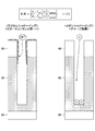
- FIG. 1 is a schematic longitudinal sectional view of an etching apparatus according to an embodiment.
- 1 is a schematic longitudinal sectional view of a film forming apparatus according to an embodiment.
- FIG. 10 is a plan view of the film forming apparatus of FIG. 9.
- 1 is a schematic longitudinal sectional view of a film forming apparatus according to an embodiment.
- FIG. 1A is a diagram showing a hole-shaped cross section according to the etching time.
- FIG. 1B is a diagram showing the relationship between the etching depth of the hole and the etching rate with respect to the etching time.
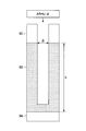
- FIG. 2A is a longitudinal sectional view of a film on a silicon wafer.
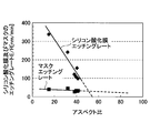
- FIG. 2B is a diagram showing the relationship between the aspect ratio of the hole and the etching rate.
- FIG. 3 is a diagram for explaining a physical phenomenon that occurs when etching a contact hole.
- the required aspect ratio (AR) of the contact hole is about 50.
- the aspect ratio (AR) is indicated by the hole depth h with respect to the diameter ⁇ of the hole opening (here, the top). Therefore, when the hole depth h is 2 ⁇ m and the hole diameter ⁇ is 40 nm, the aspect ratio is 50.
- the etching rate decreases as the hole to be etched becomes deeper.
- the etching rate is an amount that can be removed per unit time. For example, (nm / min) is used as a unit as the etching amount per minute.
- FIG. 1A shows a hole-shaped cross section corresponding to an etching time when a hole is formed in a silicon oxide (SiO 2 ) film by etching.
- SiO 2 silicon oxide
- FIG. 8 a parallel plate etching apparatus using a lower two frequency application type parallel plate etching (see FIG. 8) is used.
- Etching process conditions are as follows: the pressure is 2.66 Pa, the frequency of the high frequency power HF for plasma generation is 40 MHz, the power is 1.18 (W / cm 2 ), the frequency of the high frequency power LF for ion attraction is 3.2 MHz, It is a mixed gas having a power of 4.42 (W / cm 2 ) and a gas type of C 4 F 6 / C 4 F 8 / Ar / O 2 . Under this condition, the silicon oxide film is etched using polysilicon as a mask. In FIG. 1A, the cross-sectional shape of the hole at the etching time of 60 s, 180 s... 600 s, the numerical value of the diameter ⁇ of the hole, and the numerical value of the aspect ratio AR are shown. According to the experimental results, the hole diameter ⁇ increases and the aspect ratio AR increases as the etching depth h increases.
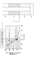
- FIG. 1B shows the etching depth (vertical axis) with respect to the etching time ET (horizontal axis).
- the depth h of the etched hole of the silicon oxide film and the pattern when etching the silicon oxide film are shown.
- the remaining amount of polysilicon mask formed is shown.
- FIG. 1B shows the etching rate of the silicon oxide film and the etching rate of the mask as the etching rate (vertical axis) with respect to the etching time ET (horizontal axis).
- the etching time ET becomes longer and the depth of the etched hole becomes deeper, so that the etching rate of the silicon oxide film decreases and the hole bottom is hard to be etched. You can see that Regardless of the etching time ET, the etching rate of the mask is substantially constant, and the reduction amount of the polysilicon mask is substantially constant.
- FIG. 2B shows the etching rate of the silicon oxide film and the etching rate of the mask with respect to the aspect ratio (horizontal axis). This shows that the etching rate of the silicon oxide film (SiO 2 ) 92 on the silicon wafer 94 is proportional to the aspect ratio (depends on the aspect ratio). From this result, it can be seen that the etching rate of the silicon oxide film decreases as the etching time in FIG. 1A progresses and the aspect ratio increases.
- FIG. 3 shows simplified physical phenomena of CF * radicals and ions when deep holes are formed by etching generated from a fluorocarbon (CF) gas.
- Radical physical phenomena include radical shadowing and radical Knudsen transport, which will be described in order.
- CF * radicals fluorocarbon radicals
- CF * radicals larger than a predetermined angle cannot enter the hole.
- the predetermined angle is determined by the depth of the hole, as the hole becomes deeper, the angle of CF * radicals that can reach the bottom of the hole is limited, and the number of CF * radicals that reach the bottom of the hole decreases. This is called radical shadowing.
- CF * radicals that enter the hole collide with the wall surface in the hole, and are adsorbed or bounced there and further proceed to the depth of the hole.
- the Knudsen transport determines the probability that the gas colliding with the wall surface in the hole will be adsorbed there, or will bounce off the wall surface and proceed toward the hole bottom and reach the hole bottom based on the adsorption coefficient.
- ions having a predetermined incident angle are incident on the holes in the plasma (the right side of FIG. 3). Ions beyond a certain angle cannot enter the hole.
- the predetermined angle at this time is determined by the depth of the hole.
- the predetermined angle is determined by the depth of the hole, as the hole becomes deeper, the angle of ions that can reach the bottom of the hole is limited, and the number of ions that reach the bottom of the hole decreases. This is called ion shadowing.
- each of radicals and ions in plasma in vacuum reduces the number of radicals and ions that reach the bottom of the hole as the hole becomes deeper, and as a result, the etching rate decreases.
- the etching rate also varies depending on the type of radical, the material of the film to be etched that forms the hole, the compatibility between the radical and the material, the temperature, and the like.
- Etching rate is expressed by the following equation (1). Based on equation (1), the main factors that influence the etching rate will be described in more detail.
- E / R A ⁇ [E i ⁇ ⁇ ion ] ⁇ [ ⁇ radical ] / ([E i ⁇ ⁇ ion ] + [ ⁇ radical ]) (1)
- A is a value determined by the type and nature of the material
- E i is ion energy
- ⁇ ion is the number of ions per unit area
- ⁇ radical is the number of radicals per unit area.
- Sputtering yield which expresses how many molecules jump out of a substance when one ion collides with the substance, influences the etching rate, and the sputtering yield correlates with the ion energy to collide. For this reason, in equation (1), ion etching rate is shown by using ion energy E i instead of sputtering yield. On the other hand, since radicals have lower energy than ions, radical etching rates are not considered in equation (1).
- the etching rate is mainly determined by the number of ions, the number of radicals and the ion energy per unit area based on the formula (1). Therefore, in the embodiment described below, by changing the material of the film in the depth direction where the etching rate decreases, the number of radicals and ions reaching the bottom of the hole decreases as the hole becomes deeper. Is suppressed.
- a laminated structure of film types according to an embodiment will be described with reference to FIG.
- a first silicon oxide film 12 and a second silicon oxide film 14 are sequentially stacked on a silicon wafer 10 formed of silicon Si, and a mask 16 is formed on the second silicon oxide film 14.
- the mask 16 is a polysilicon mask having a predetermined pattern shape to be etched.
- the silicon oxide film has a two-layer structure of the first silicon oxide film 12 and the second silicon oxide film 14, but is not limited to this.
- a structure in which the silicon content per unit volume or the volume density changes in the depth direction may be used.
- the second silicon oxide film 14 is formed of a dense SiO 2 film (hard SiO 2 ), and the first silicon oxide film 12 is relatively rougher than the second silicon oxide film 14.
- An SiO 2 film (soft SiO 2 ) is used.
- the silicon oxide film of this embodiment has a silicon content per unit volume and a volume density of the second silicon oxide film 14 of the upper layer, and the silicon content per unit volume of the first silicon oxide film 12 of the lower layer. The film is formed so as to be relatively higher than the rate and the volume density.
- the second silicon oxide film 14 can be a TEOS (Tetraethyl orthosilicate) film or a USG (Undoped Silicate Glass) film.
- TEOS film can be formed by using TEOS gas
- USG film can be formed by, for example, plasma CVD using TEOS gas and oxygen gas.
- the first silicon oxide film 12 may be, for example, a BPSG film that is a silicon oxide film doped with B (boron) and P (phosphorus).
- the silicon content per unit volume is The upper second silicon oxide film 14 so as to be relatively higher than the lower first silicon oxide film 12.
- the first silicon oxide film 12 may be a fluorine-added silicon oxide film (SiOF).
- SiOF fluorine-added silicon oxide film
- the first silicon oxide film 12 may be formed using a coating technique by SOG (Spin-On-Glass), for example. Further, the first silicon oxide film 12 may be, for example, an FSG film. The formation of the FSG film will be described later.
- plasma is generated from an etching gas containing a fluorocarbon (CF) -based gas, and the generated plasma is laminated on the silicon oxide films 12 and 14 that are etching target films. Etching of a predetermined pattern is performed using the polysilicon as a mask 16.
- CF fluorocarbon
- the silicon oxide film and the fluorocarbon react to form silicon fluoride and carbon dioxide.
- Silicon tetrafluoride and carbon dioxide are gases and are exhausted to the outside, whereby the silicon oxide film is etched.
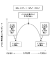
- the relationship between the ratio of carbon C and fluorine F contained in the plasma and the etching rate E / R of the silicon oxide film will be described with reference to the conceptual diagram of FIG.
- the lower the silicon content in the silicon oxide film the more the etching can be performed with fewer fluorine radicals.
- the fluorine radicals that reach the bottom of the hole decrease as the hole in the silicon oxide film becomes deeper. Therefore, when the fluorine radical that reaches the hole bottom decreases, the etching rate decreases.
- the composition of the silicon oxide film is changed in the depth direction. That is, in the present embodiment, a silicon oxide film whose silicon content or volume density decreases as the hole becomes deeper is used.
- the structure of the silicon oxide film according to the present embodiment even if the fluorine radical reaching the hole bottom decreases as the hole of the silicon oxide film becomes deeper, the decrease in the etching rate is suppressed and the etching stop is suppressed. Can be avoided.
- the silicon oxide film is formed such that the silicon content or volume density of the upper second silicon oxide film 14 is relatively higher than the silicon content or volume density of the lower first silicon oxide film 12. use. As a result, even if a deep hole bottom is formed in the lower first silicon oxide film 12, it becomes a coarse silicon oxide film compared to the upper second silicon oxide film 14. Can be suppressed.
- a method of forming a silicon oxide film in which the upper second silicon oxide film 14 is a dense film and the lower first silicon oxide film 12 is a relatively coarse film will be described.
- the dense film has a higher silicon content or volume density than the relatively rough film.
- an SOG (Spin-On-Glass) film is formed as a first silicon oxide film 12 on the silicon wafer 10 by a coating technique.
- USG is formed as the second silicon oxide film 14 by plasma CVD.
- a polysilicon layer is similarly deposited by a CVD method to form a patterned photoresist, and a polysilicon mask 16 is formed by dry etching.
- the photoresist is removed by dry etching using O 2 plasma.
- [Modification 1] Another example of generating a silicon oxide film in which the silicon content of the upper second silicon oxide film 14 is lower than the silicon content of the lower first silicon oxide film 12 is as follows. A method of mixing impurities such as boron B and phosphorus P into one silicon oxide film 12 is conceivable.
- the first silicon oxide film 12 in which impurities are mixed has a lower silicon content than the second silicon oxide film 14 in which impurities are not mixed. Accordingly, since the silicon content is reduced in the lower layer, even if the number of fluorine F radicals reaching the bottom of the deep hole formed in the first silicon oxide film 12 in the lower layer is reduced, the reduction in the etching rate is suppressed. it can.
- a silicate glass such as BPSG is formed as a first silicon oxide film 12 on the silicon wafer 10 by a high density plasma CVD method.
- a TEOS film is formed as the second silicon oxide film 14 by a CVD method in a low pressure state (pressure is higher than that in a low vacuum state), which is a slightly lower pressure than normal pressure.
- a polysilicon layer is similarly deposited by the CVD method, a patterned photoresist is formed, and a polysilicon mask is formed by dry etching. Thereafter, the photoresist is removed by dry etching using O2 plasma.
- the fluorine content per unit volume may be changed in the depth direction. That is, when the silicon oxide film is composed of two layers, a silicon oxide film in which the fluorine content of the lower first silicon oxide film 12 is higher than the fluorine content of the upper second silicon oxide film 14 is used. May be. Also by this, by containing fluorine F in the lower silicon oxide film, fluorine F is supplied from the film even at the deep hole bottom where the number of fluorine F radicals reached has decreased, so the etching rate is reduced. Can be suppressed.
- the silicon oxide film may be formed of a single layer and formed of a multilayer film in which the F content is changed so as to increase in the depth direction. According to this, the lower first silicon oxide film 12 has a higher fluorine content than the upper second silicon oxide film 14, so that the lower first silicon oxide film 12 is the upper first silicon oxide film 12. The silicon content is relatively lower than that of the second silicon oxide film 14.
- a silicon oxide film having a configuration combining the above-described embodiment and the modification 1 may be a silicon oxide film. Other configurations may also be used.
- the silicon content rate or the fluorine content rate in each of the two layers may be uniform or a film in which the content ratio changes in the depth direction.
- the upper second silicon oxide film 14 has a higher silicon content than the lower first silicon oxide film 12, and the lower first silicon oxide film 12 is higher than the upper second silicon oxide film 14.
- the fluorine content may be high.
- the silicon oxide film may be a film in which the impurity content changes in the depth direction.
- the lower first silicon oxide film 12 has a lower impurity content than the upper second silicon oxide film 14, but the impurities in each layer may be uniform, and the depth direction also in each layer.
- a film having a high impurity content may be used.
- a switching portion between the first silicon oxide film 12 and the second silicon oxide film 14 will be described with reference to FIG.
- an etching gas containing a carbon fluoride (CF) -based gas is supplied when the upper second silicon oxide film 14 is formed, and carbon fluoride (CF) is used when the lower first silicon oxide film 12 is formed.
- a fluorine F gas is supplied together with an etching gas containing a system gas.
- the horizontal axis represents the aspect ratio
- the vertical axis represents the etching rate of the silicon oxide film.
- the etching rate at the time of etching the first silicon oxide film 12 (hard SiO 2 ) is shown by the first etching rate
- the second silicon oxide film 14 a rough silicon oxide film such as a fluorine-containing film or SOG is used.
- the etching rate at the time of etching is indicated by a second etching rate.
- the lower layer first aspect ratio is set so that the aspect ratio of the hole formed by the etching method of this embodiment is the second etching rate from the portion after 50 where the first etching rate is less than 55 at which the first etching rate becomes zero.
- the portion up to the aspect ratio of 50 is configured as the upper second silicon oxide film 14, and the subsequent portions are used as the lower first silicon oxide film 12.
- the part having an aspect ratio of 40 or later is a switching part to the first silicon oxide film 12 as a lower layer so that the etching rate does not become 100 nm / min or less because of productivity problems.
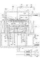
- the etching apparatus 130 has a chamber C (processing vessel) that is hermetically sealed and electrically grounded.
- the etching apparatus 130 is connected to the gas supply source 120.
- the gas supply source 120 supplies an etching gas containing a fluorocarbon (CF) -based gas as an etching gas.
- the fluorocarbon-based gas may contain hexafluoro 1,3 butadiene C 4 F 6 gas.
- the chamber C has a cylindrical shape, and is made of, for example, aluminum whose surface is anodized, and a mounting table 102 that supports the silicon wafer W is provided therein.
- the mounting table 102 also functions as a lower electrode.
- the mounting table 102 is supported by a conductive support table 104 and can be moved up and down by an elevating mechanism 107 via an insulating plate 103.
- the elevating mechanism 107 is disposed in the chamber C and is covered with a bellows 108 made of stainless steel.
- a bellows cover 109 is provided outside the bellows 108.
- a focus ring 105 made of, for example, single crystal silicon is provided on the outer periphery above the mounting table 102.
- a cylindrical inner wall member 103 a made of, for example, quartz is provided so as to surround the periphery of the mounting table 102 and the support table 104.
- a first high frequency power supply 110a is connected to the mounting table 102 via a first matching unit 111a, and high frequency power for plasma generation at a predetermined frequency (for example, 40 MHz) is supplied from the first high frequency power supply 110a. It has become.
- the mounting table 102 is connected to a second high-frequency power source 110b via a second matching unit 111b, and a high-frequency power for bias having a predetermined frequency (for example, 3.2 MHz) is supplied from the second high-frequency power source 110b. It has come to be.
- a shower head 116 that functions as an upper electrode is provided above the mounting table 102 so as to face the mounting table 102 in parallel.
- the shower head 116 and the mounting table 102 function as a pair of electrodes. It has become.
- An electrostatic chuck 106 for electrostatically adsorbing the silicon wafer W is provided on the upper surface of the mounting table 102.
- the electrostatic chuck 106 has an electrode 106a interposed between insulators 106b.
- a DC voltage source 112 is connected to the electrode 106a, and when a DC voltage is applied from the DC voltage source 112 to the electrode 106a, the silicon wafer W is adsorbed by Coulomb force.
- a coolant channel 104 a is formed inside the support body 104.
- a refrigerant inlet pipe 104b and a refrigerant outlet pipe 104c are connected to the refrigerant flow path 104a.
- the silicon wafer W is controlled to a predetermined temperature by appropriately circulating, for example, cooling water or the like as a coolant in the coolant channel 104a.
- a pipe 130 for supplying a cold transfer gas (backside gas) such as helium gas (He) is provided on the back side of the silicon wafer W.
- a cold transfer gas backside gas
- He helium gas
- the shower head 116 is provided in the ceiling portion of the chamber C.
- the shower head 116 has a main body 116a and an upper top plate 116b that forms an electrode plate.
- the shower head 116 is supported on the upper part of the chamber C through an insulating member 145.
- the main body 116a is made of a conductive material, for example, aluminum whose surface is anodized, and supports the upper top plate 116b in a detachable manner at the lower portion thereof.
- a gas diffusion chamber 126a is provided inside the main body 116a, and a large number of gas flow holes 116d are formed at the bottom of the main body 116a so as to be positioned below the diffusion chamber 126a.
- the upper top plate 116b is provided with a gas introduction hole 116e that communicates with the gas flow hole 116d so as to penetrate the upper top plate 116b in the thickness direction.
- the gas supplied to the diffusion chamber 126a is introduced into the plasma processing space in the chamber C through the gas flow hole 116d and the gas introduction hole 116e in a shower shape.
- the main body 116a and the like are provided with a pipe (not shown) for circulating the refrigerant, and the shower head 116 is cooled and adjusted to a desired temperature.
- the main body 116a is formed with a gas inlet 116g for introducing gas into the diffusion chamber 126a.
- a gas supply source 120 is connected to the gas inlet 116g.
- a variable DC voltage source 152 is electrically connected to the shower head 116 via a low pass filter (LPF) 151.
- the variable DC voltage source 152 can be turned on / off by an on / off switch 153.
- the on / off switch 153 is controlled to be turned on as necessary. As a result, a predetermined DC voltage is applied to the shower head 116.
- a cylindrical grounding conductor 101a is provided so as to extend upward from the side wall of the chamber C above the height position of the shower head 116.
- the cylindrical ground conductor 101a has a top plate on the top thereof.
- An exhaust port 171 is formed at the bottom of the chamber C.
- An exhaust device 173 is connected to the exhaust port 171.
- the exhaust device 173 includes a vacuum pump, and depressurizes the inside of the chamber C to a predetermined degree of vacuum by operating the vacuum pump.
- a gate valve 175 for loading or unloading the silicon wafer W from the loading / unloading port 174 by opening and closing is provided.
- a dipole ring magnet 124 extending annularly or concentrically is disposed around the chamber C corresponding to the vertical position at the time of processing of the mounting table 102.
- a vertical RF field is formed by the first high-frequency power source 110a, and a horizontal magnetic field is formed by the dipole ring magnet 124.
- the pressure in the processing vessel is applied to the two-layered silicon oxide film generated in this manner using, for example, a parallel plate plasma with a lower two frequency application type parallel plate etching apparatus (FIG. 8).
- a parallel plate plasma with a lower two frequency application type parallel plate etching apparatus (FIG. 8).
- high frequency power with a frequency of 40 MHz / 3.2 MHz is applied to the lower electrode at a power density of 1.18 / 4.42 (W / cm 2 ), respectively, and C 4 F 6 / C 4 F 8 / Plasma of Ar / O 2 processing gas is generated, and the silicon oxide film is etched using polysilicon as a mask.
- the depth of etching becomes deeper, and the aspect ratio described in FIG.
- the first oxide film (SOG film) having a low silicon content is obtained. Thereby, a decrease in the etching rate is suppressed, and a contact hole having a high aspect ratio, for example, 60 or more can be formed.
- FIG. 9 is a longitudinal sectional view schematically showing an example of a film forming apparatus used in the SOG film of the first embodiment.
- 10 is a plan view of the film forming apparatus of FIG.
- the film forming apparatus 140 of this embodiment used when forming an SOG film applies an SOG solution to the surface of the wafer W by a spin coating method.
- the spin chuck 48 rotated in the cup 46 by the motor M
- the processing liquid supply nozzle 50 provided at the tip of the processing liquid supply pipe 50A
- the rinse liquid supply pipe 52A A rinsing liquid supply nozzle 52 provided at the tip
- a movable arm 56 that grips these nozzles 50 and 52 and scans along the guide rod 54 in the radial direction of the wafer
- a processing liquid that waits for the processing liquid supply nozzle 50 The nozzle standby unit 56A and the dummy dispense unit 56B, the rinse liquid nozzle standby unit 60 for waiting the rinse liquid supply nozzle 52, and the exhaust pipe 62 are provided.
- the coating process in the film forming apparatus 140 will be described.
- the processing liquid supply nozzle 50 is gripped by the movable arm 56 and moved onto the wafer W.
- a SOG solution as a processing solution is dropped.
- This SOG solution is formed by mixing a film component such as a silanol compound and a solvent such as ethyl alcohol.
- the SOG solution is diffused from the central portion to the peripheral portion of the wafer W by the centrifugal force, and an SOG film is formed on the wafer W.
- the rinsing liquid supply nozzle 52 moves onto the wafer W, and the SOG film on the peripheral edge of the wafer W is dissolved and removed with a rinsing liquid such as ethyl alcohol.
- the solvent is evaporated by performing a heat treatment at a temperature of 100 ° C. to 140 ° C. in a preheating process, and then the wafer is loaded into a heating apparatus (not shown), and this is about 400 ° C. to 450 ° C.
- the SOG film is siloxane-bonded by heat treatment at a temperature of. In this way, an SOG film that is a silicon oxide film is formed.
- the applied wafer is carried into the heating apparatus and subjected to heat treatment or the like. To do.
- the pressure is 2.66 Pa, 40 MHz / 3.2 MHz.
- the high frequency power is applied at 1.18 / 4.42 (W / cm 2 ), and the silicon oxide film is etched with C 4 F 6 / C 4 F 8 / Ar / O 2 using polysilicon as a mask.
- the etching rate decreases because the first oxide film (SOG film) having a relatively lower silicon content than the second oxide film (USG film) is formed at the portion where the etching depth is deep. Therefore, contact holes having a high aspect ratio, for example, 60 or more can be formed.
- Example 2 In Example 2, a silicate glass such as a BPSG film is formed as the first silicon oxide film 12 by a high-density plasma CVD method, and a TEOS film is formed as the second silicon oxide film 14 in a slightly lower pressure than normal pressure. In a certain low pressure state (the pressure is higher than that in the low vacuum state), the film is formed by the CVD method.
- FIG. 11 is a longitudinal sectional view schematically showing an example of a film forming apparatus used in the BPSG film of Example 2.
- a film forming apparatus 301 of this embodiment used when forming a BPSG film includes a parallel plate type upper electrode 203 and a chamber 201, as shown in FIG.
- An RF power source 207 that has a lower electrode 202 and supplies RF power with a frequency of 13.56 MHz for converting the deposition gas into plasma is connected between the upper electrode 203 and the lower electrode 202.
- the inside of the chamber 201 is exhausted by an exhaust device connected to the exhaust port 205 and reduced to an appropriate pressure.
- the lower electrode 202 also serves as a mounting table on which the silicon wafer 310 is mounted, and a heating unit 206 for heating the silicon wafer 310 is provided on the lower electrode 202 side.
- the source 21 of SiOP-11 (b) as the phosphorus-containing compound source 33, the source 22 of SiH 4 as the silicon-containing compound source 36, the source of O 2 as the oxidizing gas, and Ar as the dilution gas source Alternatively, a supply source of N 2 is provided, and these supply sources are collectively connected to the gas inlet 204 of the chamber 201 of the film forming apparatus 301 by a pipe 24e.
- the RF power source 207 is connected to the upper electrode 203 through the matching circuit 208.
- pipes 24a to 24d are pipes for introducing each gas, and are connected to the flow meters 25a to 25d.
- the valves 26a to 26d open and close the source gas flow passages provided in the pipes 24a to 24d.
- the means 32 and 35 for adjusting the temperature of the source include a heater, a cooler, and the like.
- a silicon wafer 310 is placed in the chamber 201 of such a film forming apparatus 301.
- the silicon wafer 310 is heated, and the silicon wafer 310 is held within the temperature range of the film forming conditions.
- a base insulating film such as a silicon oxide film is formed on the silicon wafer 310.
- a film forming gas adjusted within the range of the film forming conditions is introduced into the chamber 201, and the film forming gas is turned into plasma with RF power of the film forming conditions.
- a PSG film (phosphorus-containing insulating film) having a predetermined film thickness containing a high concentration of phosphorus is formed.
- the PSG film may be fluidized at about the temperature of the film formation conditions during film formation. In this case, flattening is achieved simultaneously with film formation.
- a PSG film (phosphorus-containing insulating film) is formed on the silicon wafer 310, a separate heat treatment is performed to fluidize and flatten the PSG film. Thereby, a planarized PSG film is formed.
- SiH 4 is used as the silicon-containing compound
- SiOP-11 (b) is used as the phosphorus-containing compound
- an appropriate amount of oxidizing gas, for example, oxygen (O 2 ) is added. Therefore, the fluidization temperature for flattening can be drastically reduced.
- a method of forming a BPSG film containing phosphorus by plasma enhanced CVD is given.
- a mixed gas of SiH 4 + SOP-11 (b) + TMB or TEB + N 2 O was used as a film forming gas.
- the film forming conditions are as follows.
- BPSG film phosphorus-containing insulating film made of a mixture of SiO 2 + phosphorus P + boron B is formed on the silicon wafer 310.
- the pressure is 2.66 Pa, 40 MHz / 3.2 MHz.
- the high frequency power is applied at 1.18 / 4.42 (W / cm 2 ), and the silicon oxide film is etched with C 4 F 6 / C 4 F 8 / Ar / O 2 using polysilicon as a mask.
- the etching rate decreases because the first oxide film (BPSG film) having a relatively lower silicon content than the second oxide film (USG film) is formed at the location where the etching depth is deep. Therefore, contact holes having a high aspect ratio, for example, 60 or more can be formed.
- the first silicon oxide film 12 is formed of an SOG film and the second silicon oxide film 14 is formed of a USG film.
- the first silicon oxide film 12 is formed of BPSG and the second silicon oxide film is formed.
- the film 14 is formed of a TEOS film
- the first silicon oxide film 12 and the second silicon oxide film 14 may be formed by changing the combination of the two layers.
- the TEOS film is generated by plasma CVD using TEOS gas
- the USG film is generated by plasma CVD using TEOS gas and oxygen gas.
- the first silicon oxide film of the second embodiment is changed.
- An FSG film is formed as the first silicon oxide film 12 under the following process conditions using a film forming apparatus (FIG. 11) for forming a BPSG film.
- the FSG film conditions are as follows.
- SiOF film As the first silicon oxide film 12 under the following process conditions using an ICP plasma apparatus. Pressure in the growth furnace: 533.288 ⁇ 10 ⁇ 3 Pa (4 mTorr) Flow rate of silicon fluoride (SiF 4 ) gas to be introduced: 20 to 26 sccm Flow rate of SiH 4 gas to be introduced: 38 sccm O 2 gas flow rate to be introduced: 111 sccm Ar gas flow rate to be introduced: 60 sccm High frequency power (ICP power): 3.93 W / cm 2 Bias power: 2.16 W / cm 2 By forming the fluorine-containing film as the first silicon oxide film 12 in this way, the fluorine content is higher than that of the second silicon oxide film 14 (USG film or TEOS film) at the portion where the etching depth is deep.
- ICP power 3.93 W / cm 2
- Bias power 2.16 W / cm 2
- Example 4 Unlike the first silicon oxide film 12 and the second silicon oxide film 14, the flow rate of the SiF 4 gas is initially set to the flow rate of the SiH 4 gas by the film forming method of the third embodiment.
- the BPSG film and the FSG film are not limited to the plasma CVD film forming apparatus shown in FIG. 11, and the film forming apparatus for forming the SOG film shown in FIG. 9 may be used.
- the film forming apparatus for forming the SOG film shown in FIG. 9 may be used.
- any of a film forming apparatus in which an SOG film is formed and a plasma CVD film forming apparatus can be used.
- the object to be processed in the present invention is not limited to the silicon wafer used in the description in the above embodiment, and for example, a large substrate for a flat panel display, an EL element, or a solar cell It may be a substrate for use.
Landscapes
- Physics & Mathematics (AREA)
- Engineering & Computer Science (AREA)
- Plasma & Fusion (AREA)
- Chemical & Material Sciences (AREA)
- Analytical Chemistry (AREA)
- Drying Of Semiconductors (AREA)
- Internal Circuitry In Semiconductor Integrated Circuit Devices (AREA)
- Formation Of Insulating Films (AREA)
Abstract
Description
前記プラズマにより、シリコン酸化膜に積層された所定パターンのポリシリコンのマスクを介して、単位体積当たりのシリコン含有率、単位体積当たりのフッ素含有率及び体積密度の少なくともいずれかが深さ方向に変化する前記シリコン酸化膜をエッチングするステップと、
が提供される。
前記処理容器は、単位体積当たりのシリコン含有率、単位体積当たりのフッ素含有率及び体積密度の少なくともいずれかが深さ方向に変化するシリコン酸化膜と該シリコン酸化膜に積層された所定パターンのポリシリコンのマスクが積層された被処理体を収容し、
前記ガス供給源は、処理容器内に前記フッ化炭素(CF)系ガスを含むエッチングガスを供給し、
前記エッチングガスから生成されたプラズマにより、前記所定パターンのポリシリコンのマスクを介して前記シリコン酸化膜をエッチングする、
ことを特徴とするエッチング装置が提供される。
高いアスペクト比を有するコンタクトホール(穴)では、ホール底が深くなるに従いエッチングレートが低くなる。この現象を図1A,図1B,図2A,図2B,図3を参照しながら説明する。図1Aは、エッチングタイムに応じた穴形状の断面を示した図である。図1Bは、エッチングタイムに対する穴のエッチング深さとエッチングレートとの関係を示した図である。図2Aは、シリコンウエハ上の膜の縦断面図である。図2Bは、穴のアスペクト比とエッチングレートとの関係を示した図である。図3は、コンタクトホールのエッチングの際に生じる物理現象を説明する図である。
ここで、Aは材料の種類や性質により定まる値であり、Eiはイオンエネルギーである。Γionは単位面積当たりのイオン数であり、Γradicalは単位面積当たりのラジカル数である。
一実施形態に係る膜種の積層構造について、図4を参照しながら説明する。シリコンSiにて形成されたシリコンウエハ10上には、第1のシリコン酸化膜12、第2のシリコン酸化膜14が順に積層され、第2のシリコン酸化膜14上にマスク16が形成されている。マスク16は、エッチングしたい所定のパターンの形状を有したポリシリコンマスクである。本実施形態では、シリコン酸化膜は、第1のシリコン酸化膜12と第2のシリコン酸化膜14の2層構造になっているが、これに限られず、3層以上又は1層であって、単位体積当たりのシリコン含有率又は体積密度が深さ方向に変化する構造であってもよい。
SiO2+CF4→SiF4↑(ガス)+CO2↑(ガス)・・・(2)
プラズマ中に含有される炭素Cとフッ素Fの比率とシリコン酸化膜のエッチングレートE/Rの関係について、図5の概念図を参照して説明する。プラズマ中の炭素C含有率とフッ素F含有率の比率のバランスがよいグラフの中央部分では、シリコン酸化膜中のSi、Oに対して、上記SiF4↑+CO2↑の反応が促進され、上記反応が促進されるため、シリコン酸化膜のエッチングレートE/Rは高くなる。一方、プラズマ中の炭素C含有率がフッ素含有率より低くなっているグラフの左部分では、炭素Cが少ないため、上記SiF4↑+CO2↑の反応のうち、図6に示したCO2↑のガス化が促進されないため、シリコン酸化膜がエッチングされにくくなってシリコン酸化膜のエッチングレートE/Rは下がる。同様に、プラズマ中のフッ素含有率が炭素C含有率より低いグラフの右部分では、上記SiF4↑+CO2↑の反応のうち、図6に示したSiF4↑のガス化が促進されないため、シリコン酸化膜がエッチングされにくくなってシリコン酸化膜のエッチングレートE/Rは下がる。よって、シリコン酸化膜のE/Rはプラズマ中の構成要素に左右され、例えば、フッ素Fラジカルが少ないとエッチングレートE/Rは下がる。
上層の第2のシリコン酸化膜14のシリコン含有率が下層の第1のシリコン酸化膜12のシリコン含有率より低いシリコン酸化膜を生成する他の例としては、シリコン酸化膜の成膜時、第1のシリコン酸化膜12にボロンBやリンP等の不純物を混入させる方法が考えられる。不純物を混入させた第1のシリコン酸化膜12は、不純物を混入させていない第2のシリコン酸化膜14よりシリコン含有率が低い。よって、下層にてシリコン含有率が低下するため、下層の第1のシリコン酸化膜12に形成された深穴の穴底に到達するフッ素Fラジカルの数が低下してもエッチングレートの低下を抑制できる。
単位体積当たりのシリコン含有率を深さ方向に変化させる方法のうち、単位体積当たりのフッ素含有率を深さ方向に変化させてもよい。つまり、シリコン酸化膜が2層から構成されている場合、下層の第1のシリコン酸化膜12のフッ素含有率が上層の第2のシリコン酸化膜14のフッ素含有率より高いシリコン酸化膜を使用してもよい。これによっても、下層のシリコン酸化膜中にフッ素Fを含有することにより、フッ素Fラジカルの到達数が低下した深穴の穴底であっても膜からフッ素Fが供給されるのでエッチングレートの低下を抑制できる。シリコン酸化膜を一層で構成し、F含有率が深さ方向に高くなるように変化させた多層膜により形成されてもよい。これによれば、下層の第1のシリコン酸化膜12は、上層の第2のシリコン酸化膜14よりフッ素含有率が相対的に高い分、下層の第1のシリコン酸化膜12は、上層の第2のシリコン酸化膜14よりシリコン含有率が相対的に低くなっている。
第1のシリコン酸化膜12と第2のシリコン酸化膜14との切り替え部分について、図7を参照しながら説明する。ここでは、上層の第2のシリコン酸化膜14の成膜時にはフッ化炭素(CF)系ガスを含むエッチングガスが供給され、下層の第1のシリコン酸化膜12の成膜時にはフッ化炭素(CF)系ガスを含むエッチングガスとともにフッ素Fガスが供給される。
次に、一実施形態に係る図4に示した積層膜の穴部を形成するために使用されるエッチング装置の一例を、図8に基づき説明する。
次に、一実施形態に係る図4に示した第1のシリコン酸化膜12及び第2のシリコン酸化膜14の積層膜の成膜を形成するために使用される成膜装置の一例を、実施例1~実施例3の順に説明する。
(実施例1)
実施例1では、第1のシリコン酸化膜12としてSOG膜を成膜し、第2のシリコン酸化膜14としてUSG膜をプラズマCVDで成膜する。図9は、実施例1のSOG膜で使用する膜形成装置の一例を概略的に示した縦断面図である。図10は、図9の膜形成装置の平面図である。
(実施例2)
実施例2では、第1のシリコン酸化膜12としてBPSG膜などのシリケードガラスを高密プラズマCVD法で成膜し、第2のシリコン酸化膜14としてTEOS膜を常圧よりも少し低い圧力状態である低圧力状態(低真空状態よりも圧力は高い。)において、CVD法で成膜する。図11は、実施例2のBPSG膜で使用する成膜装置の一例を概略的に示した縦断面図である。
ガス圧力:0.5~3.0Torr(66.66~399.9Pa)
SOP-11(b)バブリングガス(N2又はAr)、流量:300~1500sccm(SOP-11(b)、ソース温度:45℃
SiH4、流量:100~2000sccm
TMP、流量:15~600sccm
TMB又はTEB、流量:10~300sccm
酸化性ガス(O2)、流量:300sccm以下
RF電力:0.147~1.18W/cm2
周波数:100kHz~2.5GHz
上記により、シリコンウエハ310上にSiO2+リンP+ボロンBの混合物からなるBPSG膜(リン含有絶縁膜)が形成される。
(実施例3)
実施例3では、実施例2の第1のシリコン酸化膜を変更した実施例である。第1のシリコン酸化膜12としてFSG膜を、BPSG膜を形成するための成膜装置(図11)を用いて下記のようなプロセス条件で成膜する。
FSG膜条件は以下の通りである。
ガス圧力:533.288×10⁻³Pa
SiF4ガスの流量:26sccm
SiH4ガスの流量:38sccm
O2ガスの流量:111sccm
Arガスの流量:60sccm
RF電力:2.16W/cm2
上記により、シリコンウエハにFSG膜が形成される。FSG膜のフッ素含有率を変更するにはSiF4ガスとSiH4ガスのガス比を変更すればよい。つまり、深さ方向にフッ素含有率が高くなるように、SiH4ガスに対するSiF4ガスの流量を多くする。
成長炉内の圧力:533.288×10⁻³Pa(4mTorr)
導入するフッ化シリコン(SiF4)ガスの流量:20~26sccm
導入するSiH4ガスの流量:38sccm
導入するO2ガスの流量:111sccm
導入するArガスの流量:60sccm
高周波電力(ICP power):3.93W/cm2
バイアス電力(Bias power):2.16W/cm2
このように第1のシリコン酸化膜12としてフッ素含有膜を形成することで、エッチングの深さが深くなった箇所で、第2のシリコン酸化膜14(USG膜やTEOS膜)よりもフッ素含有率が高い第1の酸化膜(FSG)となる。よって、深いホールの底のエッチングに際に、フッ素ラジカルが供給されやすくなるためエッチングレートの低下が抑制され、高いアスペクト比、例えば、60以上のコンタクトホールを形成することができる。
(実施例4)
第1のシリコン酸化膜12及び第2のシリコン酸化膜14のように2層ではなく、実施例3の成膜方法によって、例えば、最初はSiF4ガスの流量をSiH4ガスの流量に対して上昇させフッ素含有率が高いシリコン酸化膜をホールの深い部分で形成し、少しずつSiF4ガスの流量をSiH4ガスの流量に対して減少させていく複数のステップで多層膜を形成する方法を採用することも可能である。
12 第1のシリコン酸化膜
14 第2のシリコン酸化膜
16 マスク
130 エッチング装置
140 膜形成装置
201 チャンバ
301 成膜装置
Claims (12)
- 処理容器内にフッ化炭素(CF)系ガスを含むエッチングガスを供給し、前記エッチングガスからプラズマを生成するステップと、
前記プラズマにより、シリコン酸化膜に積層された所定パターンのポリシリコンのマスクを介して、単位体積当たりのシリコン含有率、単位体積当たりのフッ素含有率及び体積密度の少なくともいずれかが深さ方向に変化する前記シリコン酸化膜をエッチングするステップと、
を含むことを特徴とするエッチング方法。 - 前記シリコン酸化膜のシリコン含有率又は体積密度が、深さ方向に低くなることを特徴とする請求項1に記載のエッチング方法。
- 前記シリコン酸化膜のフッ素含有率は、深さ方向に高くなることを特徴とする請求項1に記載のエッチング方法。
- 前記シリコン酸化膜は、2層から構成され、
前記単位体積当たりのシリコン含有率又は体積密度は、上層のシリコン酸化膜が下層のシリコン酸化膜より高いことを特徴とする請求項1に記載のエッチング方法。 - 前記シリコン酸化膜は、2層から構成され、
前記単位体積当たりのフッ素含有率は、下層のシリコン酸化膜が上層のシリコン酸化膜より高いことを特徴とする請求項1に記載のエッチング方法。 - 前記シリコン酸化膜は、不純物の含有率が変化することを特徴とする請求項1に記載のエッチング方法。
- 前記シリコン酸化膜は、2層から構成され、
前記シリコン酸化膜の上層は、TEOS膜又はUSG膜であり、下層はBPSG膜又はSiOF膜又はFSG膜であることを特徴とする請求項1に記載のエッチング方法。 - 前記シリコン酸化膜は、前記エッチング方法により形成された穴の開口部の直径に対する穴の深さを示すアスペクト比が50以下で前記シリコン酸化膜の上層から下層に切り替わるように形成されていることを特徴とする請求項4に記載のエッチング方法。
- 前記シリコン酸化膜は、前記エッチング方法により形成された穴の開口部の直径に対する穴の深さを示すアスペクト比が40以下で前記シリコン酸化膜の上層から下層に切り替わるように形成されていることを特徴とする請求項8に記載のエッチング方法。
- 前記フッ化炭素系ガスは、ヘキサフルオロ1,3ブタジエンC4F6ガスを含有することを特徴とする請求項1に記載のエッチング方法。
- 前記シリコン酸化膜は、CVD(Chemical Vapor Deposition)又はSOG(Spin-On-Glass)により成膜されることを特徴とする請求項1に記載のエッチング方法。
- 処理容器とガス供給源とを備えるエッチング装置であって、
前記処理容器は、単位体積当たりのシリコン含有率、単位体積当たりのフッ素含有率及び体積密度の少なくともいずれかが深さ方向に変化するシリコン酸化膜と該シリコン酸化膜に積層された所定パターンのポリシリコンのマスクが積層された被処理体を収容し、
前記ガス供給源は、処理容器内に前記フッ化炭素(CF)系ガスを含むエッチングガスを供給し、
前記エッチングガスから生成されたプラズマにより、前記所定パターンのポリシリコンのマスクを介して前記シリコン酸化膜をエッチングする、
ことを特徴とするエッチング装置。
Priority Applications (2)
| Application Number | Priority Date | Filing Date | Title |
|---|---|---|---|
| US14/402,780 US9396968B2 (en) | 2012-06-25 | 2013-06-24 | Etching method and etching apparatus |
| KR1020147033006A KR102151278B1 (ko) | 2012-06-25 | 2013-06-24 | 에칭 방법 및 에칭 장치 |
Applications Claiming Priority (4)
| Application Number | Priority Date | Filing Date | Title |
|---|---|---|---|
| JP2012141660A JP2014007270A (ja) | 2012-06-25 | 2012-06-25 | エッチング方法及びエッチング装置 |
| JP2012-141660 | 2012-06-25 | ||
| US201261667527P | 2012-07-03 | 2012-07-03 | |
| US61/667,527 | 2012-07-03 |
Publications (1)
| Publication Number | Publication Date |
|---|---|
| WO2014002965A1 true WO2014002965A1 (ja) | 2014-01-03 |
Family
ID=49783111
Family Applications (1)
| Application Number | Title | Priority Date | Filing Date |
|---|---|---|---|
| PCT/JP2013/067288 Ceased WO2014002965A1 (ja) | 2012-06-25 | 2013-06-24 | エッチング方法及びエッチング装置 |
Country Status (4)
| Country | Link |
|---|---|
| US (1) | US9396968B2 (ja) |
| JP (1) | JP2014007270A (ja) |
| KR (1) | KR102151278B1 (ja) |
| WO (1) | WO2014002965A1 (ja) |
Families Citing this family (5)
| Publication number | Priority date | Publication date | Assignee | Title |
|---|---|---|---|---|
| JP6216300B2 (ja) | 2014-09-15 | 2017-10-18 | 東芝メモリ株式会社 | 半導体装置及びその製造方法 |
| JP2017098478A (ja) * | 2015-11-27 | 2017-06-01 | 東京エレクトロン株式会社 | エッチング方法 |
| RU2687299C1 (ru) * | 2018-08-17 | 2019-05-13 | Акционерное общество "Научно-исследовательский институт физических измерений" | Способ получения рельефа в диэлектрической подложке |
| KR102760678B1 (ko) * | 2019-11-28 | 2025-02-04 | 삼성전자주식회사 | 3차원 반도체 메모리 장치 |
| US11380697B2 (en) * | 2020-02-25 | 2022-07-05 | Tokyo Electron Limited | Raised pad formations for contacts in three-dimensional structures on microelectronic workpieces |
Citations (2)
| Publication number | Priority date | Publication date | Assignee | Title |
|---|---|---|---|---|
| JPH11307516A (ja) * | 1998-04-23 | 1999-11-05 | Sanyo Electric Co Ltd | 半導体装置の製造方法 |
| JP2003133293A (ja) * | 2001-10-30 | 2003-05-09 | Mitsubishi Electric Corp | 半導体装置の製造方法 |
Family Cites Families (3)
| Publication number | Priority date | Publication date | Assignee | Title |
|---|---|---|---|---|
| US6297163B1 (en) * | 1998-09-30 | 2001-10-02 | Lam Research Corporation | Method of plasma etching dielectric materials |
| US6831018B2 (en) * | 2001-08-21 | 2004-12-14 | Matsushita Electric Industrial Co., Ltd. | Method for fabricating semiconductor device |
| JP2004063512A (ja) | 2002-07-25 | 2004-02-26 | Matsushita Electric Ind Co Ltd | コンタクトホールのエッチング方法 |
-
2012
- 2012-06-25 JP JP2012141660A patent/JP2014007270A/ja active Pending
-
2013
- 2013-06-24 KR KR1020147033006A patent/KR102151278B1/ko not_active Expired - Fee Related
- 2013-06-24 WO PCT/JP2013/067288 patent/WO2014002965A1/ja not_active Ceased
- 2013-06-24 US US14/402,780 patent/US9396968B2/en not_active Expired - Fee Related
Patent Citations (2)
| Publication number | Priority date | Publication date | Assignee | Title |
|---|---|---|---|---|
| JPH11307516A (ja) * | 1998-04-23 | 1999-11-05 | Sanyo Electric Co Ltd | 半導体装置の製造方法 |
| JP2003133293A (ja) * | 2001-10-30 | 2003-05-09 | Mitsubishi Electric Corp | 半導体装置の製造方法 |
Also Published As
| Publication number | Publication date |
|---|---|
| US20150140821A1 (en) | 2015-05-21 |
| KR102151278B1 (ko) | 2020-09-02 |
| JP2014007270A (ja) | 2014-01-16 |
| US9396968B2 (en) | 2016-07-19 |
| KR20150024316A (ko) | 2015-03-06 |
Similar Documents
| Publication | Publication Date | Title |
|---|---|---|
| US9406523B2 (en) | Highly selective doped oxide removal method | |
| US9412608B2 (en) | Dry-etch for selective tungsten removal | |
| KR100978704B1 (ko) | 밀도 및 스텝 커버리지가 개선된 비정질 탄소막 증착 방법 | |
| KR102038608B1 (ko) | 반도체 장치의 제조 방법 | |
| TWI576914B (zh) | Pattern forming method and substrate processing system | |
| TWI530995B (zh) | 用於蝕刻sin膜的方法 | |
| TWI775839B (zh) | 具有選擇性阻隔層的結構 | |
| US9607811B2 (en) | Workpiece processing method | |
| JP7401593B2 (ja) | 空隙を形成するためのシステム及び方法 | |
| US9881806B2 (en) | Method of manufacturing a semiconductor device | |
| JP2017098478A (ja) | エッチング方法 | |
| TW201320220A (zh) | 用於處理晶圓及清潔腔室之感應電漿源 | |
| TW201440138A (zh) | 用於鹵化物驅氣的處理系統及方法 | |
| JP6050944B2 (ja) | プラズマエッチング方法及びプラズマ処理装置 | |
| WO2012173122A1 (ja) | プラズマエッチング方法 | |
| KR102151278B1 (ko) | 에칭 방법 및 에칭 장치 | |
| JP7634642B2 (ja) | ホウ素がドープされたシリコン材料を利用した集積プロセス | |
| JP2014003085A (ja) | プラズマエッチング方法及びプラズマ処理装置 | |
| US20230343598A1 (en) | Method For Improving Etch Rate And Critical Dimension Uniformity When Etching High Aspect Ratio Features Within A Hard Mask Layer | |
| US9305795B2 (en) | Plasma processing method | |
| TWI497586B (zh) | Plasma etching method | |
| JP5452133B2 (ja) | プラズマ処理装置およびプラズマ処理方法 | |
| KR101324941B1 (ko) | 비정질 탄소막 형성 방법 |
Legal Events
| Date | Code | Title | Description |
|---|---|---|---|
| 121 | Ep: the epo has been informed by wipo that ep was designated in this application |
Ref document number: 13808685 Country of ref document: EP Kind code of ref document: A1 |
|
| WWE | Wipo information: entry into national phase |
Ref document number: 14402780 Country of ref document: US |
|
| ENP | Entry into the national phase |
Ref document number: 20147033006 Country of ref document: KR Kind code of ref document: A |
|
| NENP | Non-entry into the national phase |
Ref country code: DE |
|
| 122 | Ep: pct application non-entry in european phase |
Ref document number: 13808685 Country of ref document: EP Kind code of ref document: A1 |