WO2014002807A1 - 電子部品のキャンパッケージ構造 - Google Patents
電子部品のキャンパッケージ構造 Download PDFInfo
- Publication number
- WO2014002807A1 WO2014002807A1 PCT/JP2013/066543 JP2013066543W WO2014002807A1 WO 2014002807 A1 WO2014002807 A1 WO 2014002807A1 JP 2013066543 W JP2013066543 W JP 2013066543W WO 2014002807 A1 WO2014002807 A1 WO 2014002807A1
- Authority
- WO
- WIPO (PCT)
- Prior art keywords
- stem
- support base
- case
- opening
- package structure
- Prior art date
- Legal status (The legal status is an assumption and is not a legal conclusion. Google has not performed a legal analysis and makes no representation as to the accuracy of the status listed.)
- Ceased
Links
Images


Classifications
-
- H—ELECTRICITY
- H10—SEMICONDUCTOR DEVICES; ELECTRIC SOLID-STATE DEVICES NOT OTHERWISE PROVIDED FOR
- H10W—GENERIC PACKAGES, INTERCONNECTIONS, CONNECTORS OR OTHER CONSTRUCTIONAL DETAILS OF DEVICES COVERED BY CLASS H10
- H10W76/00—Containers; Fillings or auxiliary members therefor; Seals
- H10W76/10—Containers or parts thereof
- H10W76/12—Containers or parts thereof characterised by their shape
- H10W76/13—Containers comprising a conductive base serving as an interconnection
- H10W76/136—Containers comprising a conductive base serving as an interconnection having other interconnections perpendicular to the conductive base
-
- G—PHYSICS
- G01—MEASURING; TESTING
- G01J—MEASUREMENT OF INTENSITY, VELOCITY, SPECTRAL CONTENT, POLARISATION, PHASE OR PULSE CHARACTERISTICS OF INFRARED, VISIBLE OR ULTRAVIOLET LIGHT; COLORIMETRY; RADIATION PYROMETRY
- G01J1/00—Photometry, e.g. photographic exposure meter
- G01J1/02—Details
- G01J1/0271—Housings; Attachments or accessories for photometers
-
- G—PHYSICS
- G01—MEASURING; TESTING
- G01J—MEASUREMENT OF INTENSITY, VELOCITY, SPECTRAL CONTENT, POLARISATION, PHASE OR PULSE CHARACTERISTICS OF INFRARED, VISIBLE OR ULTRAVIOLET LIGHT; COLORIMETRY; RADIATION PYROMETRY
- G01J5/00—Radiation pyrometry, e.g. infrared or optical thermometry
- G01J5/02—Constructional details
-
- G—PHYSICS
- G01—MEASURING; TESTING
- G01J—MEASUREMENT OF INTENSITY, VELOCITY, SPECTRAL CONTENT, POLARISATION, PHASE OR PULSE CHARACTERISTICS OF INFRARED, VISIBLE OR ULTRAVIOLET LIGHT; COLORIMETRY; RADIATION PYROMETRY
- G01J5/00—Radiation pyrometry, e.g. infrared or optical thermometry
- G01J5/02—Constructional details
- G01J5/04—Casings
- G01J5/041—Mountings in enclosures or in a particular environment
- G01J5/045—Sealings; Vacuum enclosures; Encapsulated packages; Wafer bonding structures; Getter arrangements
-
- H—ELECTRICITY
- H10—SEMICONDUCTOR DEVICES; ELECTRIC SOLID-STATE DEVICES NOT OTHERWISE PROVIDED FOR
- H10W—GENERIC PACKAGES, INTERCONNECTIONS, CONNECTORS OR OTHER CONSTRUCTIONAL DETAILS OF DEVICES COVERED BY CLASS H10
- H10W76/00—Containers; Fillings or auxiliary members therefor; Seals
- H10W76/10—Containers or parts thereof
- H10W76/12—Containers or parts thereof characterised by their shape
-
- H—ELECTRICITY
- H10—SEMICONDUCTOR DEVICES; ELECTRIC SOLID-STATE DEVICES NOT OTHERWISE PROVIDED FOR
- H10W—GENERIC PACKAGES, INTERCONNECTIONS, CONNECTORS OR OTHER CONSTRUCTIONAL DETAILS OF DEVICES COVERED BY CLASS H10
- H10W90/00—Package configurations
-
- H—ELECTRICITY
- H10—SEMICONDUCTOR DEVICES; ELECTRIC SOLID-STATE DEVICES NOT OTHERWISE PROVIDED FOR
- H10W—GENERIC PACKAGES, INTERCONNECTIONS, CONNECTORS OR OTHER CONSTRUCTIONAL DETAILS OF DEVICES COVERED BY CLASS H10
- H10W99/00—Subject matter not provided for in other groups of this subclass
-
- Y—GENERAL TAGGING OF NEW TECHNOLOGICAL DEVELOPMENTS; GENERAL TAGGING OF CROSS-SECTIONAL TECHNOLOGIES SPANNING OVER SEVERAL SECTIONS OF THE IPC; TECHNICAL SUBJECTS COVERED BY FORMER USPC CROSS-REFERENCE ART COLLECTIONS [XRACs] AND DIGESTS
- Y10—TECHNICAL SUBJECTS COVERED BY FORMER USPC
- Y10T—TECHNICAL SUBJECTS COVERED BY FORMER US CLASSIFICATION
- Y10T29/00—Metal working
- Y10T29/49—Method of mechanical manufacture
- Y10T29/49826—Assembling or joining
- Y10T29/49945—Assembling or joining by driven force fit
Definitions
- the present invention relates to an electronic component package structure, and more particularly, to an electronic component can package structure including a stem and a can case.
- the can package is used for a package structure that is hermetically sealed and has high environmental resistance, a package structure such as a sensor having a window, or a package structure that requires an electrostatic shield.
- a package structure such as a sensor having a window
- a package structure that requires an electrostatic shield for example, Patent Document 1 discloses a pyroelectric infrared sensor having a can package structure.
- an alumina substrate, a FET, and a support base on which a rectangular predetermined electrode pattern is formed are arranged on the stem, and a window portion is formed on the can case.
- An optical filter is bonded to the window.
- the can case is firmly fixed to the stem and sealed.
- the can package including the stem and the can case is configured by fitting the opening of the can case to the stem support base and resistance welding.
- the outer diameter of the stem support base and the inner diameter of the opening of the can case have a fitting tolerance, and when the can case is put on the stem, the outer diameter of the stem support base and the can case A predetermined gap is formed between the opening and the inner diameter of the opening. That is, a gap is provided in advance so that “fitting” at the time of assembly is possible even if the outer diameter of the disc-shaped support base portion of the stem and the inner diameter of the opening portion of the can case vary in size.
- An object of the present invention is to provide a can package structure with high assembling accuracy by preventing the deviation between the can case and the stem during assembly and storage and improving workability.
- the can package structure of the present invention includes a stem having a disk-shaped support base, and a can case in which an opening is fitted to the support base of the stem. At least the opening of the can case is elliptical in a state before being fitted to the support base of the stem, and the minor axis direction of the elliptical shape is slightly smaller than the diameter of the support base of the stem, The opening of the can case matches the shape of the support base portion of the stem by elastic deformation of the can case in the fitted state.
- the present invention has the following effects.
- the can case and the stem can be securely fitted to each other before resistance welding, and a shift during storage can be prevented.
- FIG. 1 is an exploded perspective view of a pyroelectric infrared sensor 10 according to an embodiment of the present invention.
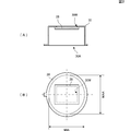
- 2A is a cross-sectional view of the can case with the optical filter 28 attached thereto
- FIG. 2B is a bottom view as seen from the opening side of the can case with the optical filter 28 attached. is there.
- FIG. 3 is a plan view of the pyroelectric infrared sensor 10 as viewed from the window side.
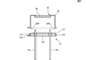
- FIG. 4 is a cross-sectional view showing a state when the can case 30 is fitted into the stem 12.
- FIG. 1 is an exploded perspective view of a pyroelectric infrared sensor 10 according to an embodiment of the present invention.
- 2A is a cross-sectional view of the cancase with the optical filter 28 attached thereto
- FIG. 2B is a bottom view of the cancase with the optical filter 28 attached as seen from the opening side.
- FIG. 3 is a plan view of the pyroelectric infrared sensor 10 as viewed from the window side.
- the pyroelectric infrared sensor 10 shown in FIG. 1 includes a metal stem 12 and a metal can case 30.
- the stem 12 includes a disk-shaped support base (stem base) 12a.
- stem base 12a In the support base 12a, three terminal pins 14a to 14c are formed penetrating the support base 12a in the thickness direction. Among these, the terminal pins 14a and 14b are attached to the support base 12a (hermetically sealed) through the glass material 16, and the terminal pin 14c is directly attached to the support base 12a.
- a hook-like member for floating and supporting the alumina substrate 20 from the support base 12a is projected and formed in a direction perpendicular to the axial direction of the terminal pins 14a to 14c. ing.
- the FET 18 is attached to the lower surface of the alumina substrate 20.
- a plurality of predetermined electrode patterns 22 are formed on the alumina substrate 20.
- Each terminal of the FET 18 is electrically connected to each electrode pattern 22 of the alumina substrate 20.
- recesses 20a to 20c for fitting the terminal pins 14a to 14c are formed.
- the terminal pins 14a to 14c are fitted into the recesses 20a to 20c, and are electrically connected to and fixed to the electrode patterns 22 by a conductive paste or the like.
- a support base 24 having a substantially concave cross section is fixed to the upper surface of the alumina substrate 20.
- the support base 24 functions as a high resistance body for supporting the pyroelectric element 26 and obtaining an output voltage.
- the support table 24 is electrically connected to the corresponding electrode pattern 22 at both ends.
- the support 24 may be formed of a material such as borosilicate glass or alkali-free glass in that it has low thermal conductivity, mechanical strength, and a resistance value of about 10 11 ⁇ . preferable.
- a dual type pyroelectric element 26 is disposed on the upper surface of the support base 24.
- the vicinity of both ends in the longitudinal direction is fixed to and electrically connected to the convex portions 24a and 24a 'of the support base 24, respectively.
- a window 30W is opened in the can case 30, and the optical filter 28 is bonded to the window 30W.
- the opening of the can case 30 is resistance-welded to the outer peripheral portion of the support base 12a of the stem 12 so that the inside of the package is sealed.
- the can case 30 has an oval shape before being fitted into the support 12a of the stem 12 (single unit state).
- the support base 12a of the stem 12 is circular.
- the outer diameter of the support base 12a is smaller than the long diameter MAA of the opening 30A of the can case 30 and larger than the short diameter MIA.
- the opening 30A of the can case is fitted into the support base portion 12a of the stem. That is, the major axis of the opening 30A has a margin with respect to the outer diameter of the stem support base 12a, and the gap corresponding to the margin acts as a margin for shrinkage. Since the short diameter of the opening 30A is smaller than the outer diameter of the stem support base 12a, the support base 12a is sandwiched by this short diameter.
- FIG. 4 is a cross-sectional view showing a state when the can case 30 is fitted into the stem 12.
- This cross section is a plane passing through the short axis MIA shown in FIG.
- the support base 12a includes a tapered portion 12T that contacts the opening 30R of the can case, and a vertical portion 12V that extends from the tapered portion 12T to the flange portion of the stem 12.
- the inner peripheral edge 30R of the opening of the can case is rounded.
- the inner peripheral edge 30R of the opening of the can case slides on the tapered portion 12T of the support base portion 12a of the stem, and the shape of the opening that has been elliptical is changed to a circle. To do.
- the opening of the can case sandwiches the vertical portion 12V of the stem support base in the minor axis direction.
- the tapered portion 12T may have a round shape.
- the can case can be deformed and fitted into the stem simply by press-fitting the can case 30 into the stem 12.
- the opening 30A may be covered with the stem support base 12a in a state of being elastically deformed so as to be substantially circular. If the pressure is released, the can case also holds the stem support 12a due to its elasticity.
- the opening of the can case is fitted into the support base portion 12 a of the stem 12. Since the short diameter part of 30A elastically clamps the support base part 12a of the stem, it is possible to maintain the state in which the opening part 30A of the cancase is fitted in the support base part 12a of the stem 12, and to prevent a shift during storage.
- the deviation is suppressed when the can case opening 30A is set to the resistance welding electrode in order to resistance weld the outer periphery of the support base 12a of the stem. Therefore, the workability of resistance welding is improved. Furthermore, since the resistance welding is performed in a state where the stem 12 and the can case 30 are held at a predetermined fitting strength, they are prevented from being displaced by a shock during welding.
- the positioning during welding can be set up offline, the resistance welding work can be performed efficiently, and the tact of the equipment can be improved.
- FIGS. 2 and 3 show examples in which the entire cylindrical portion of the cancase is an elliptical cylinder. However, a cross-sectional view from the bottom (surface opposite to the opening) of the cancase to the opening is seen. In this case, even if the bottom is circular and the shape gradually becomes elliptical as it approaches the opening, the same effect is obtained.
- the pyroelectric infrared sensor shown in the embodiment is an example, and it goes without saying that the present invention can be applied to various electronic component can package structures including a stem and a can case.
- MAA major axis MIA ... minor axis 10
- pyroelectric infrared sensor 12 ... stem 12a ... support bases 14a, 14b, 14c ... terminal pin 16 ... glass material 18
- FET 20 ... Alumina substrate 20a ... Recess 22
- Electrode pattern 24 ... Support base 26 . Pyroelectric element 28 .
- Optical filter 30 ... Can case 30A ... Opening 30W ... Window
Landscapes
- Physics & Mathematics (AREA)
- General Physics & Mathematics (AREA)
- Spectroscopy & Molecular Physics (AREA)
- Photometry And Measurement Of Optical Pulse Characteristics (AREA)
Abstract
Description
前記キャンケースの少なくとも前記開口部は前記ステムの支持台部に嵌め合わされる前の状態で楕円形状であり、当該楕円形状の短軸方向は前記ステムの支持台部の径よりも僅かに小さく、嵌め合わされた状態で前記キャンケースの弾性変形により前記キャンケースの開口部は前記ステムの支持台部の形状に一致していることを特徴とする。
MIA…短径
10…焦電型赤外線センサ
12…ステム
12a…支持台部
14a,14b,14c…端子ピン
16…ガラス材
18…FET
20…アルミナ基板
20a…凹部
22…電極パターン
24…支持台
26…焦電素子
28…光学フィルタ
30…キャンケース
30A…開口部
30W…窓部
Claims (1)
- 円板状の支持台部を備えたステムと、このステムの支持台部に開口部が嵌め合わされるキャンケースと、を備えた電子部品のキャンパッケージ構造において、
前記キャンケースの少なくとも前記開口部は前記ステムの支持台部に嵌め合わされる前の状態で楕円形状であり、当該楕円形状の短軸方向は前記ステムの支持台部の径よりも僅かに小さく、嵌め合わされた状態で前記キャンケースの弾性変形により前記キャンケースの開口部は前記ステムの支持台部の形状に一致していることを特徴とする、電子部品のキャンパッケージ構造。
Priority Applications (4)
| Application Number | Priority Date | Filing Date | Title |
|---|---|---|---|
| JP2014522547A JP5850151B2 (ja) | 2012-06-28 | 2013-06-17 | 電子部品のキャンパッケージ構造 |
| CN201380034426.2A CN104412379B (zh) | 2012-06-28 | 2013-06-17 | 电子部件的罐封装件结构 |
| DE112013003198.1T DE112013003198T5 (de) | 2012-06-28 | 2013-06-17 | Elektronikbauteil-Dosenverpackungsstruktur |
| US14/573,798 US9299625B2 (en) | 2012-06-28 | 2014-12-17 | Electronic component can package structure |
Applications Claiming Priority (2)
| Application Number | Priority Date | Filing Date | Title |
|---|---|---|---|
| JP2012145535 | 2012-06-28 | ||
| JP2012-145535 | 2012-06-28 |
Related Child Applications (1)
| Application Number | Title | Priority Date | Filing Date |
|---|---|---|---|
| US14/573,798 Continuation US9299625B2 (en) | 2012-06-28 | 2014-12-17 | Electronic component can package structure |
Publications (1)
| Publication Number | Publication Date |
|---|---|
| WO2014002807A1 true WO2014002807A1 (ja) | 2014-01-03 |
Family
ID=49782968
Family Applications (1)
| Application Number | Title | Priority Date | Filing Date |
|---|---|---|---|
| PCT/JP2013/066543 Ceased WO2014002807A1 (ja) | 2012-06-28 | 2013-06-17 | 電子部品のキャンパッケージ構造 |
Country Status (5)
| Country | Link |
|---|---|
| US (1) | US9299625B2 (ja) |
| JP (1) | JP5850151B2 (ja) |
| CN (1) | CN104412379B (ja) |
| DE (1) | DE112013003198T5 (ja) |
| WO (1) | WO2014002807A1 (ja) |
Families Citing this family (1)
| Publication number | Priority date | Publication date | Assignee | Title |
|---|---|---|---|---|
| JP1624076S (ja) * | 2018-04-16 | 2019-02-12 |
Citations (2)
| Publication number | Priority date | Publication date | Assignee | Title |
|---|---|---|---|---|
| JPH08128895A (ja) * | 1994-09-05 | 1996-05-21 | Murata Mfg Co Ltd | 焦電型赤外線検出器 |
| JP2000100981A (ja) * | 1998-09-17 | 2000-04-07 | Nec Kansai Ltd | 電子素子封入容器及びこれを用いた電子部品 |
Family Cites Families (7)
| Publication number | Priority date | Publication date | Assignee | Title |
|---|---|---|---|---|
| US5270555A (en) * | 1989-05-18 | 1993-12-14 | Murata Manufacturing Co., Ltd. | Pyroelectric IR-sensor with a molded inter connection device substrate having a low thermal conductivity coefficient |
| JPH06112342A (ja) * | 1992-09-29 | 1994-04-22 | Shinko Electric Ind Co Ltd | ガラス端子 |
| US5898256A (en) | 1995-08-30 | 1999-04-27 | Miyota Co., Ltd. | Container for enclosing a piezo-electric transducer |
| JP2002314143A (ja) * | 2001-04-09 | 2002-10-25 | Toshiba Corp | 発光装置 |
| JP3743394B2 (ja) * | 2002-05-31 | 2006-02-08 | 株式会社村田製作所 | 赤外線センサおよびそれを用いた電子装置 |
| US7671335B2 (en) * | 2005-11-22 | 2010-03-02 | Panasonic Electric Works Co., Ltd. | Infrared detector and process for fabricating the same |
| CN102575983A (zh) * | 2009-06-25 | 2012-07-11 | 松下电器产业株式会社 | 红外线式气体检测器以及红外线式气体测量装置 |
-
2013
- 2013-06-17 JP JP2014522547A patent/JP5850151B2/ja active Active
- 2013-06-17 CN CN201380034426.2A patent/CN104412379B/zh active Active
- 2013-06-17 DE DE112013003198.1T patent/DE112013003198T5/de not_active Withdrawn
- 2013-06-17 WO PCT/JP2013/066543 patent/WO2014002807A1/ja not_active Ceased
-
2014
- 2014-12-17 US US14/573,798 patent/US9299625B2/en active Active
Patent Citations (2)
| Publication number | Priority date | Publication date | Assignee | Title |
|---|---|---|---|---|
| JPH08128895A (ja) * | 1994-09-05 | 1996-05-21 | Murata Mfg Co Ltd | 焦電型赤外線検出器 |
| JP2000100981A (ja) * | 1998-09-17 | 2000-04-07 | Nec Kansai Ltd | 電子素子封入容器及びこれを用いた電子部品 |
Also Published As
| Publication number | Publication date |
|---|---|
| JP5850151B2 (ja) | 2016-02-03 |
| US20150170984A1 (en) | 2015-06-18 |
| DE112013003198T5 (de) | 2015-03-12 |
| US9299625B2 (en) | 2016-03-29 |
| CN104412379B (zh) | 2017-02-22 |
| CN104412379A (zh) | 2015-03-11 |
| JPWO2014002807A1 (ja) | 2016-05-30 |
Similar Documents
| Publication | Publication Date | Title |
|---|---|---|
| JP6571513B2 (ja) | 蓄電装置 | |
| CN106169554B (zh) | 汇流条及电池模块 | |
| CN107425334B (zh) | 连接器 | |
| WO2016110886A1 (ja) | 蓄電ユニット | |
| US20190221954A1 (en) | Externally-attached ptc element and tubular battery | |
| JP5850151B2 (ja) | 電子部品のキャンパッケージ構造 | |
| US20130180751A1 (en) | Assembling structure of bus bar | |
| JP6670170B2 (ja) | チップ形電解コンデンサ及びその製造方法 | |
| JP2009168845A (ja) | 圧電ブザー | |
| JP6662737B2 (ja) | ヒューズ | |
| CN110750023A (zh) | 镜头模组以及电子设备 | |
| WO2012111245A1 (ja) | ガスセンサ及びその中間部品 | |
| JP6135123B2 (ja) | 圧電素子ユニットおよび圧電アクチュエータ | |
| JP6655499B2 (ja) | ヒューズ | |
| JP6997565B2 (ja) | 流体性状検出装置 | |
| US10553523B2 (en) | Semiconductor device | |
| US20170047504A1 (en) | Piezoelectric sounding body | |
| US10460872B2 (en) | Electronic device | |
| WO2015170589A1 (ja) | コンデンサ | |
| JP2006041125A (ja) | チップ形アルミニウム電解コンデンサ | |
| JP2016181473A (ja) | 外付けptc素子および筒型電池 | |
| JP2009147012A (ja) | 回路装置及びその製造方法 | |
| JP2801121B2 (ja) | 電子部品用キャップ | |
| JP2021170448A (ja) | バッテリー端子 | |
| TW201942920A (zh) | 金屬氧化物變阻器及其製造方法 |
Legal Events
| Date | Code | Title | Description |
|---|---|---|---|
| 121 | Ep: the epo has been informed by wipo that ep was designated in this application |
Ref document number: 13808801 Country of ref document: EP Kind code of ref document: A1 |
|
| ENP | Entry into the national phase |
Ref document number: 2014522547 Country of ref document: JP Kind code of ref document: A |
|
| WWE | Wipo information: entry into national phase |
Ref document number: 112013003198 Country of ref document: DE Ref document number: 1120130031981 Country of ref document: DE |
|
| 122 | Ep: pct application non-entry in european phase |
Ref document number: 13808801 Country of ref document: EP Kind code of ref document: A1 |