WO2014002328A1 - スパッタリング装置およびスパッタリング方法 - Google Patents
スパッタリング装置およびスパッタリング方法 Download PDFInfo
- Publication number
- WO2014002328A1 WO2014002328A1 PCT/JP2013/001095 JP2013001095W WO2014002328A1 WO 2014002328 A1 WO2014002328 A1 WO 2014002328A1 JP 2013001095 W JP2013001095 W JP 2013001095W WO 2014002328 A1 WO2014002328 A1 WO 2014002328A1
- Authority
- WO
- WIPO (PCT)
- Prior art keywords
- substrate
- target
- holder
- sputtering
- center
- Prior art date
- Legal status (The legal status is an assumption and is not a legal conclusion. Google has not performed a legal analysis and makes no representation as to the accuracy of the status listed.)
- Ceased
Links
Images










Classifications
-
- H—ELECTRICITY
- H01—ELECTRIC ELEMENTS
- H01J—ELECTRIC DISCHARGE TUBES OR DISCHARGE LAMPS
- H01J37/00—Discharge tubes with provision for introducing objects or material to be exposed to the discharge, e.g. for the purpose of examination or processing thereof
- H01J37/32—Gas-filled discharge tubes
- H01J37/34—Gas-filled discharge tubes operating with cathodic sputtering
- H01J37/3411—Constructional aspects of the reactor
- H01J37/3435—Target holders (includes backing plates and endblocks)
-
- C—CHEMISTRY; METALLURGY
- C23—COATING METALLIC MATERIAL; COATING MATERIAL WITH METALLIC MATERIAL; CHEMICAL SURFACE TREATMENT; DIFFUSION TREATMENT OF METALLIC MATERIAL; COATING BY VACUUM EVAPORATION, BY SPUTTERING, BY ION IMPLANTATION OR BY CHEMICAL VAPOUR DEPOSITION, IN GENERAL; INHIBITING CORROSION OF METALLIC MATERIAL OR INCRUSTATION IN GENERAL
- C23C—COATING METALLIC MATERIAL; COATING MATERIAL WITH METALLIC MATERIAL; SURFACE TREATMENT OF METALLIC MATERIAL BY DIFFUSION INTO THE SURFACE, BY CHEMICAL CONVERSION OR SUBSTITUTION; COATING BY VACUUM EVAPORATION, BY SPUTTERING, BY ION IMPLANTATION OR BY CHEMICAL VAPOUR DEPOSITION, IN GENERAL
- C23C14/00—Coating by vacuum evaporation, by sputtering or by ion implantation of the coating forming material
- C23C14/22—Coating by vacuum evaporation, by sputtering or by ion implantation of the coating forming material characterised by the process of coating
- C23C14/225—Oblique incidence of vaporised material on substrate
-
- C—CHEMISTRY; METALLURGY
- C23—COATING METALLIC MATERIAL; COATING MATERIAL WITH METALLIC MATERIAL; CHEMICAL SURFACE TREATMENT; DIFFUSION TREATMENT OF METALLIC MATERIAL; COATING BY VACUUM EVAPORATION, BY SPUTTERING, BY ION IMPLANTATION OR BY CHEMICAL VAPOUR DEPOSITION, IN GENERAL; INHIBITING CORROSION OF METALLIC MATERIAL OR INCRUSTATION IN GENERAL
- C23C—COATING METALLIC MATERIAL; COATING MATERIAL WITH METALLIC MATERIAL; SURFACE TREATMENT OF METALLIC MATERIAL BY DIFFUSION INTO THE SURFACE, BY CHEMICAL CONVERSION OR SUBSTITUTION; COATING BY VACUUM EVAPORATION, BY SPUTTERING, BY ION IMPLANTATION OR BY CHEMICAL VAPOUR DEPOSITION, IN GENERAL
- C23C14/00—Coating by vacuum evaporation, by sputtering or by ion implantation of the coating forming material
- C23C14/22—Coating by vacuum evaporation, by sputtering or by ion implantation of the coating forming material characterised by the process of coating
- C23C14/34—Sputtering
-
- C—CHEMISTRY; METALLURGY
- C23—COATING METALLIC MATERIAL; COATING MATERIAL WITH METALLIC MATERIAL; CHEMICAL SURFACE TREATMENT; DIFFUSION TREATMENT OF METALLIC MATERIAL; COATING BY VACUUM EVAPORATION, BY SPUTTERING, BY ION IMPLANTATION OR BY CHEMICAL VAPOUR DEPOSITION, IN GENERAL; INHIBITING CORROSION OF METALLIC MATERIAL OR INCRUSTATION IN GENERAL
- C23C—COATING METALLIC MATERIAL; COATING MATERIAL WITH METALLIC MATERIAL; SURFACE TREATMENT OF METALLIC MATERIAL BY DIFFUSION INTO THE SURFACE, BY CHEMICAL CONVERSION OR SUBSTITUTION; COATING BY VACUUM EVAPORATION, BY SPUTTERING, BY ION IMPLANTATION OR BY CHEMICAL VAPOUR DEPOSITION, IN GENERAL
- C23C14/00—Coating by vacuum evaporation, by sputtering or by ion implantation of the coating forming material
- C23C14/22—Coating by vacuum evaporation, by sputtering or by ion implantation of the coating forming material characterised by the process of coating
- C23C14/34—Sputtering
- C23C14/3407—Cathode assembly for sputtering apparatus, e.g. Target
-
- C—CHEMISTRY; METALLURGY
- C23—COATING METALLIC MATERIAL; COATING MATERIAL WITH METALLIC MATERIAL; CHEMICAL SURFACE TREATMENT; DIFFUSION TREATMENT OF METALLIC MATERIAL; COATING BY VACUUM EVAPORATION, BY SPUTTERING, BY ION IMPLANTATION OR BY CHEMICAL VAPOUR DEPOSITION, IN GENERAL; INHIBITING CORROSION OF METALLIC MATERIAL OR INCRUSTATION IN GENERAL
- C23C—COATING METALLIC MATERIAL; COATING MATERIAL WITH METALLIC MATERIAL; SURFACE TREATMENT OF METALLIC MATERIAL BY DIFFUSION INTO THE SURFACE, BY CHEMICAL CONVERSION OR SUBSTITUTION; COATING BY VACUUM EVAPORATION, BY SPUTTERING, BY ION IMPLANTATION OR BY CHEMICAL VAPOUR DEPOSITION, IN GENERAL
- C23C14/00—Coating by vacuum evaporation, by sputtering or by ion implantation of the coating forming material
- C23C14/22—Coating by vacuum evaporation, by sputtering or by ion implantation of the coating forming material characterised by the process of coating
- C23C14/34—Sputtering
- C23C14/35—Sputtering by application of a magnetic field, e.g. magnetron sputtering
-
- C—CHEMISTRY; METALLURGY
- C23—COATING METALLIC MATERIAL; COATING MATERIAL WITH METALLIC MATERIAL; CHEMICAL SURFACE TREATMENT; DIFFUSION TREATMENT OF METALLIC MATERIAL; COATING BY VACUUM EVAPORATION, BY SPUTTERING, BY ION IMPLANTATION OR BY CHEMICAL VAPOUR DEPOSITION, IN GENERAL; INHIBITING CORROSION OF METALLIC MATERIAL OR INCRUSTATION IN GENERAL
- C23C—COATING METALLIC MATERIAL; COATING MATERIAL WITH METALLIC MATERIAL; SURFACE TREATMENT OF METALLIC MATERIAL BY DIFFUSION INTO THE SURFACE, BY CHEMICAL CONVERSION OR SUBSTITUTION; COATING BY VACUUM EVAPORATION, BY SPUTTERING, BY ION IMPLANTATION OR BY CHEMICAL VAPOUR DEPOSITION, IN GENERAL
- C23C14/00—Coating by vacuum evaporation, by sputtering or by ion implantation of the coating forming material
- C23C14/22—Coating by vacuum evaporation, by sputtering or by ion implantation of the coating forming material characterised by the process of coating
- C23C14/50—Substrate holders
- C23C14/505—Substrate holders for rotation of the substrates
-
- H—ELECTRICITY
- H01—ELECTRIC ELEMENTS
- H01J—ELECTRIC DISCHARGE TUBES OR DISCHARGE LAMPS
- H01J37/00—Discharge tubes with provision for introducing objects or material to be exposed to the discharge, e.g. for the purpose of examination or processing thereof
- H01J37/32—Gas-filled discharge tubes
- H01J37/34—Gas-filled discharge tubes operating with cathodic sputtering
- H01J37/3402—Gas-filled discharge tubes operating with cathodic sputtering using supplementary magnetic fields
- H01J37/3405—Magnetron sputtering
-
- H—ELECTRICITY
- H01—ELECTRIC ELEMENTS
- H01J—ELECTRIC DISCHARGE TUBES OR DISCHARGE LAMPS
- H01J37/00—Discharge tubes with provision for introducing objects or material to be exposed to the discharge, e.g. for the purpose of examination or processing thereof
- H01J37/32—Gas-filled discharge tubes
- H01J37/34—Gas-filled discharge tubes operating with cathodic sputtering
- H01J37/3411—Constructional aspects of the reactor
- H01J37/3414—Targets
- H01J37/3417—Arrangements
Definitions
- the present invention relates to a sputtering apparatus and a sputtering method for forming a thin film using a sputtering method (hereinafter also simply referred to as sputtering).
- Patent Document 1 As a technique for satisfactorily forming a film thickness distribution in the substrate surface using a target smaller than the substrate size, an oblique incident rotation sputtering method in which the target is disposed diagonally opposite the substrate is widely used (for example, Patent Document 1). ).
- the projection surface projected in the substrate normal direction in the direction of the center normal of the target is positioned outside the surface of the substrate. It is necessary to dispose the target away from the substrate along a direction parallel to the substrate surface, or to dispose the target and the substrate with a smaller inclination (that is, with the target and the substrate closer to parallel).
- the target As the size of the substrate increases, the target must be arranged further away from the center point of the substrate.
- the target projection surface is also projected in the substrate direction. For this reason, in order to avoid the target projection plane from within the substrate plane, it is necessary to increase the distance between the target and the substrate or to arrange the target and the substrate in a state of being more parallel. As a result, the amount of film formation at a point far from the target in the substrate surface is remarkably reduced, and even if the film is formed while rotating the substrate, a sufficient film thickness distribution cannot be obtained.
- the present invention has been made with the above-described problem as an opportunity, and provides a sputtering apparatus and method that can obtain a sufficient film thickness distribution in the substrate surface even when the target projection surface is not projected onto the substrate. Objective.
- a first aspect of the present invention is a sputtering apparatus, a processing chamber for processing a substrate, a substrate holder disposed in the processing chamber, and the substrate holder A target holder inclined to the substrate holder and opposed to the substrate holder, and a method of centering the target holding surface of the target holder with respect to a surface including the substrate placement surface of the substrate holder
- the projection surface of the target holding surface projected in a line direction is formed outside the substrate placement surface of the substrate holder, and the center normal of the substrate placement surface and the center normal of the target holder are the same It is not on the surface.
- a sputtering apparatus a processing chamber for processing a substrate, a substrate holder disposed in the processing chamber, and diagonally opposite the substrate holder, the substrate A first holder that is perpendicular to a surface including the substrate placement surface of the substrate holder and passes through a center point of the target holding surface of the target holder.
- an angle formed by the center normal of the target holding surface is ⁇ , the first surface including the first line and the center normal of the substrate mounting surface, and the substrate mounting surface of the substrate holder
- ⁇ is 15 ° ⁇ ⁇ ⁇ 60 °
- the substrate mounting surface With respect to the plane on which includes a projection plane of the target holding surface projected onto the center normal direction of the target holding surface, characterized in that it is formed outside the substrate mounting surface of the substrate holder
- a sputtering method wherein the target is positioned obliquely with respect to the substrate and is disposed so as to be opposed to the substrate while being inclined, and the substrate is rotated with respect to the substrate.
- the center normal of the surface to be processed of the substrate does not exist on the same plane as the center normal of the target surface, and the surface includes the surface to be processed.
- the sputtering process is performed on the substrate in a state where the substrate is placed so that a projection surface of the target surface projected in the direction of the center normal of the target surface is formed outside the surface to be processed.
- a film treatment is performed.
- the sputtering apparatus and method of the present invention it is possible to obtain a sufficient film thickness distribution in the substrate plane even when the target projection plane is not projected onto the substrate.
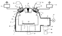
- FIG. 1 is a diagram schematically showing a film forming apparatus 1 according to this embodiment.
- the film forming apparatus 1 includes a vacuum container 2 as a substrate processing chamber.
- the vacuum vessel 2 is connected to a vacuum exhaust device having a turbo molecular pump 48 and a dry pump 49 that exhaust the vacuum vessel 2 through an exhaust port 8.
- the film forming apparatus 1 includes a gas introduction mechanism 15 that can introduce a discharge gas into the vacuum vessel 2.
- the exhaust port 8 is a conduit having a rectangular cross section, for example, and connects the vacuum vessel 2 and the turbo molecular pump 48.
- a main valve 47 is provided between the exhaust port 8 and the turbo molecular pump 48.
- a target 4 having a surface to be sputtered exposed is held by a target holder 6.
- a substrate holder 7 for placing the substrate 10 is provided at a predetermined position where the sputtered particles emitted from the target 4 arrive.
- the substrate 10 is carried in and out through the gate valve 42 provided in the vacuum vessel 2.
- a mask 11 may be provided around the substrate placement surface of the substrate holder 7 to prevent film adhesion to the end, side wall, and back surface of the substrate 10.
- the substrate holder 7 is configured to be able to rotate the substrate mounting surface on which the substrate 10 is mounted, and is configured to be able to rotate the substrate 10 within the surface in a state where the substrate 10 is mounted.
- the rotation axis of the substrate holder 7 and the rotation axis of the substrate 10 are configured to coincide with each other.
- the rotation of the substrate holder 7 is controlled by the substrate holder drive mechanism 31.
- the vacuum vessel 2 is provided with a pressure gauge 41 for measuring the pressure of the vacuum vessel 2.
- a grounded cylindrical shield 40 (an adhesion shield member) is provided on the inner surface of the vacuum vessel 2. The shield 40 prevents sputtered particles from directly attaching to the inner surface of the vacuum vessel 2.
- the number of targets is two, but a larger number may be used.
- the gas inlet is provided beside both targets, but it is not limited to this position and may be provided at other positions.
- the target 4 is disposed diagonally opposite the substrate 10 and is inclined to face the substrate 10.
- the target 4 having a diameter smaller than that of the substrate 10 is used.
- the target 4 by providing the target 4 with the substrate holder 7 and the substrate 10 facing each other at an inclined position, a good film can be formed within the substrate plane even when the target 4 having a small diameter is used. A thickness distribution is obtained.
- the target 4 is inclined with respect to the substrate holder 7 and the substrate 10, as shown in FIG. 1, when an unused target having a flat standard surface is used, the surface and the substrate 10. This means that the surface is not parallel.
- the target holder 6 is connected to a power source 12 for applying sputtering discharge power.
- the present invention is not limited to this.
- the target 4 is an insulator
- an RF power source is used.
- a voltage is applied to the target 4 by the power source 12 to form plasma, whereby sputtering is performed.
- a magnetron unit 19 is disposed on the back surface of the target holder 6, and magnetic lines for confining plasma are formed in the vicinity of the target 4.
- the target holder 6 is insulated from the vacuum vessel 2 by an insulator. Since the target holder 6 is made of a metal such as Cu, it becomes an electrode when DC or RF power is applied. As is well known, the target 4 is composed of material components to be deposited on the substrate. Since it relates to the purity of the film, a high purity is desirable.
- a target shutter 13 may be provided between the target holder 6 and the substrate holder 7.
- the target shutter 13 is controlled by a target shutter drive mechanism 14 and is configured to be switchable between an open state in which the target 4 and the substrate 10 face each other or a closed state in which the target 4 and the substrate 10 are shielded from each other.
- the gas introduction mechanism 15 includes a pipe for introducing a discharge gas, a cylinder for storing the gas, a mass flow controller for controlling the gas flow rate, valves for shutting off and starting the gas flow, It consists of a pressure reducing valve and a filter. Furthermore, the gas introduction mechanism 15 is configured to allow a designated gas flow rate to flow stably by the control device. Further, a mixed gas obtained by mixing a reactive gas with a discharge gas may be introduced from the gas introduction mechanism 15. Other introduction mechanisms for introducing the reactive gas may be provided.
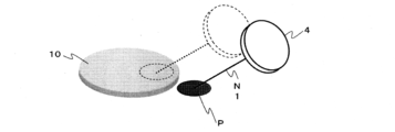
- FIGS. 2, 3A and 3B are diagrams for explaining the positional relationship between the conventional target 4 and the substrate 10.
- FIG. 2 the projection plane P of the target 4 projected onto the surface of the substrate 10 is projected onto the substrate 10 along the direction of the center normal line N ⁇ b> 1 of the target 4.
- the target 4 is separated from the substrate 10 so as to increase the distance between the target 4 and the substrate 10 as shown in FIG. 3A so that the projection plane P does not overlap the substrate 10.
- the inclination of the target 4 and the substrate 10 is made smaller. In the method shown in FIGS.
- the film formation speed is not linear on the surface of the substrate 10, that is, has an irregular distribution. It is difficult to obtain a similar film thickness.
- the broken lines in FIGS. 3A and 3B indicate the position of the target 4 and the position of the normal line N1 in the state of FIG. 2 and the projection plane thereof on FIGS. 3A and 3B, respectively.
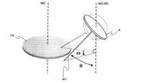
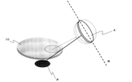
- FIG. 4 is a view for explaining the positional relationship between the target 4 and the substrate 10 according to the present embodiment.
- the projection surface P is rotated about the rotation axis R with respect to the conventional target 4 so that the projection surface P does not overlap the substrate 10, that is, the projection surface P is formed outside the substrate 10.
- the target 4 is arranged at the position where it has been moved.
- the normal line N ⁇ b> 3 that includes the surface of the substrate 10 and passes through the center of the target 4 is the rotation axis R.
- the rotation axis R is used to compare and describe the positional relationship between the target 4 and the substrate 10 in the conventional sputtering apparatus and the positional relationship between the target 4 and the substrate 10 in the sputtering apparatus according to the present embodiment. It is. That is, in the sputtering apparatus according to this embodiment, the target 4 and the target holder 6 that holds the target 4 are not actually driven to rotate about the rotation axis R.
- the projection plane can be obtained without increasing the distance (offset distance) between the center of the target 4 and the substrate 10. P can be removed from the surface to be processed of the substrate 10. As a result, it is possible to perform a film forming process on the substrate 10 with a good in-plane distribution while reducing damage to the coating film caused by negative ions.
- the center normal N1 and the center normal N2 of the substrate 10 intersect on the substrate 10 side with respect to the target 4 (in the following description, the angle ⁇ is It may be explained by omitting +).
- the offset distance is a distance between the center normal line N2 of the substrate 10 and the normal line N3.
- the TS distance is a distance of the normal line N3 from the center position of the surface of the target 4 to the surface S including the surface of the substrate 10.
- the angle ⁇ is a rotation angle when the normal line N1 and the normal line N2 are in the same plane as 0 degrees, and the normal line N1 is rotated about the normal line N3 as the rotation axis.
- FIG. 7 shows a state when the substrate 10 and the target 4 are viewed from above.
- the angle ⁇ will be described with reference to FIG. 7.
- the center of the surface of the target 4 the plane including the center normal N ⁇ b> 2 of the substrate 10, and the center normal of the four targets parallel to the center normal N ⁇ b> 2 of the substrate 10. It is also an angle formed with the surface including N1.
- ⁇ is 0 degree when the normal line N1 and the normal line N2 are in the same plane, so that the rotation angle is equivalent as long as the rotation angle is the same regardless of the direction of rotation. For example, if one rotation angle is + and the other rotation angle is-, + 30 ° and -30 ° are equivalent.
- the angle ⁇ is not particularly limited as long as the film formation process on the substrate 10 is possible, but considering the in-plane distribution of the film thickness when the film is formed on the substrate 10 and the adhesion efficiency of sputtered particles on the substrate, It is preferable that 15 degrees ⁇ ⁇ ⁇ 60 degrees.
- the angle ⁇ is not particularly limited as long as the film forming process can be performed on the substrate 10, but the in-plane distribution of the film thickness when the film is formed on the substrate 10, and the adhesion efficiency of the sputtered particles on the substrate Is considered, it is preferable that 15 degrees ⁇
- the angle ⁇ and the angle ⁇ are also used to explain the positional relationship between the target 4 and the substrate 10 in the sputtering apparatus according to the present embodiment, like the rotation axis R. That is, in the sputtering apparatus according to the present embodiment, the target 4 and the target holder 6 are not actually rotated in the directions of the angle ⁇ and the angle ⁇ .
- the center normal of the substrate 10 is a line perpendicular to the surface to be processed of the substrate 10 at the center point of the substrate 10.
- the center normal of the target 4 is a line perpendicular to the surface to be sputtered of the target 4 at the center point of the surface to be sputtered of the target 4.
- the surface to be sputtered of the target 4 refers to a target having a flat surface when not used. When the surface of the target 4 is processed into a predetermined shape, the perpendicular is obtained based on the back surface of the target 4 or a flat surface such as the target holder 6.
- the size of the substrate 10 that can be placed on the substrate holder 7 from the configuration of the substrate holder 7 or other general components is as follows. Limited.
- the target holder 6 is also limited in the form of the target 4 held by the target holder 6 from other general components (for example, means for fixing the target, form of the target holder 6, shield on the outer periphery). That is, since the projection surface P of the target 4 does not overlap the surface of the substrate 10, the target 4 of the target holder 6 is held with respect to the surface including the substrate placement surface on which the substrate 10 of the substrate holder 7 is placed.
- the apparatus is arranged so that the projection surface obtained by projecting the target holding surface in the center normal direction of the target holding surface does not overlap the substrate mounting surface, that is, the projection surface is formed outside the substrate mounting surface. What is necessary is just to comprise.
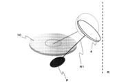
- FIG. 8 shows a state in which the projection plane P is projected on the substrate 10.
- the target 4 is arranged at a position rotated around the rotation axis R that does not pass through the center of the target 4 from the state shown in FIG. 8, and the projection plane P is out of the plane of the substrate 10. positioned.
- the rotation axis R is an arbitrary normal of the surface including the surface of the substrate 10.
- FIG. 10 shows the positional relationship between the target 4 and the substrate 10 according to this embodiment.
- the broken line is the state shown in FIG. 8, and the solid line is the state shown in FIG.
- FIG. 11 it can be seen that the offset distance is changed by rotating around the rotation axis R. That is, the distance between the center C1 of the substrate 10 and the center C2 of the target 4 when the projection plane P exists on the substrate 10, and the center C1 and the center C2 ′ when the projection plane P does not exist on the substrate 10. It can be seen that the distance is changing.
- this embodiment can be considered essentially the same as the first embodiment.
- the target 4 is rotated with the line segment passing through the center C2 ′ as the rotation axis R. It can be considered that the target 4 is arranged at the position. That is, in this embodiment, both the offset distance and the angle ⁇ are changed.
- the projection plane P is projected onto the surface of the substrate 10 while reducing the increase amount of the offset distance compared to the conventional method of changing only the offset distance. Can be avoided.
- FIG. 12 shows a state in which the projection plane P is projected onto the substrate 10 as in FIG. As shown in FIG. 13, the projection surface P is located outside the surface of the substrate 10 by arranging the target 4 at a position where the target 4 is rotated around the rotation axis R.
- This embodiment is essentially the same as the first embodiment.
- the angle ⁇ since the line segment parallel to the surface of the target 4 is the rotation axis R, the angle ⁇ also changes. That is, it can be said that this embodiment changes both the angle ⁇ and the angle ⁇ with reference to the state of FIG.
- the target 4 is disposed at the position where the target 4 is rotated with the line segment having the normal component in the plane of the substrate 10 as the rotation axis R.
- the projection plane P is prevented from overlapping the surface of the substrate 10. That is, conventionally, in order not to overlap the projection plane P on the surface of the substrate 10, a method of separating the target 4 from the substrate or reducing the angle ⁇ has been adopted. It can be said that the angle 4 has the target 4 disposed at a position where the target 4 is rotated with a line segment parallel to the surface of the substrate 10 as a rotation axis.
- the offset distance between the target 4 and the substrate 10 is not changed or the offset distance is changed. It is possible to avoid the projection plane P from overlapping the surface of the substrate 10 while reducing the amount of increase in comparison with the prior art. In other words, when arranging the target 4 and the substrate 10 so that the projection plane P does not overlap the surface to be processed of the substrate 10, the normal line N1 and the normal line N2 do not exist on the same plane.
- the target drive unit 9 may be provided in the target holder 6 in order to adjust the angle ⁇ . For this reason, even when the material of the target 4 attached to the target holder 6 is changed, the angle ⁇ can be set according to the required film characteristics.
- the target driving unit 9 may be further configured to adjust the angle ⁇ .
- one or more drive units that can change the position of the substrate placement surface with respect to the target 4 may be provided. In this case, the angle ⁇ of the target 4 with respect to the substrate 10 can be adjusted by changing the position of the substrate 10 in the in-plane direction of the substrate 10 with respect to the target 4.
- an outer edge portion of about several millimeters from the outer periphery of the substrate 10 may be discarded without being used for an electronic device or the like. In such a case, it is only necessary that the projection plane P is out of the effective use area used for manufacturing the electronic device or the like of the substrate 10.
- a plurality of targets 4 according to Embodiments 1 to 3 may be disposed.
- a film forming process may be performed using a plurality of targets 4 according to the first to third embodiments simultaneously.
- two targets 4 according to the first embodiment may be arranged symmetrically with respect to the normal line N2, and the film forming process on the substrate 10 may be performed by simultaneously sputtering the two targets 4. In this way, the in-plane distribution of the substrate 10 can be improved.
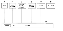
- the control device includes a main control unit 100, and the storage device 63 provided in the main control unit 100 stores control programs for executing various substrate processing processes according to the present invention.
- the control program is implemented as a mask ROM.
- the control program can be installed in a storage device 63 configured by a hard disk drive (HDD) or the like via an external recording medium or a network.
- the main controller 100 is electrically connected to the power source 12 for applying the sputtering discharge power, the gas introduction mechanism 15, the substrate holder driving mechanism 31, the target shutter driving mechanism 14, the pressure gauge 41, the gate valve 42, and the like.
- the operation of the sputtering apparatus can be managed and controlled.
- Example 1 A first example of the simulation according to the first embodiment will be described with reference to FIGS.
- Sputtering was RF sputtering using a MgO target.
- the target diameter was 164 mm, and the tilt angle ⁇ of the target with respect to the substrate was 30 °.
- the diameter of the substrate was 200 mm.
- the offset distance between the target and the substrate was 250 mm.
- the in-plane rotation of the substrate by the substrate holder was 60 rpm.
- Example 2 A second example based on the simulation in the first embodiment will be described with reference to FIGS.
- Sputtering was RF sputtering using a MgO target.
- the target diameter was 164 mm, and the tilt angle ⁇ of the target with respect to the substrate was 30 °.
- the diameter of the substrate was 300 mm.
- the offset distance between the target and the substrate was 270 mm.
- the in-plane rotation of the substrate by the substrate holder was 60 rpm.
- the film forming apparatus 1 is configured so that the projection plane P of the target 4 does not overlap the substrate 10. It can be considered that the target 4 is equal to the target mounting portion of the target holder 6 and the substrate 10 is equal to the substrate mounting surface on the substrate holder 7.
- the size of the substrate 10 used in the sputtering apparatus can be determined by another general module used in a normal sputtering apparatus. That is, the substrate mounting surface can also be determined by another general module in a normal sputtering apparatus. And the effect of this invention can be acquired by setting predetermined angle (omega) so that the projection surface of the target attachment part to the surface containing a substrate mounting surface may remove
- FIG. 18 is a cross-sectional view of the substrate holder 7, the substrate 10, and the mask 11 on the plane including the center normal line N 2 and the normal line N 3 of the substrate 10.
- the line L is a line segment in contact with the end portion of the mask 11 and has an inclination angle similar to the inclination angle of the target 4 with respect to the substrate 10.
- FIG. 19 shows the angle ⁇ , when the mask 11 is provided, the shadow formed on the surface of the substrate 10 by the mask 11 is considered for both the angle ⁇ and the angle ⁇ .
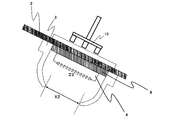
- a region obtained by projecting a circle having a diameter X2 centered on the normal line N1 formed by the deposition preventing member 3 onto the target 4 in a direction perpendicular to the target 4 is defined as Z2.
- a target projection plane P is formed by this region Z2. That is, when the outer edge of the target 4 is covered with the deposition preventing member 3, the target projection surface P formed by the region Z ⁇ b> 2 does not overlap the substrate 10, i.e., the projection surface P is formed outside the substrate 10. It ’s fine.
- the projection plane P when the magnetron sputtering method is used as the sputtering method of the target 4 will be described with reference to FIG.
- a magnetron unit 19 is disposed on the back surface of the target holder 6, and the magnetic lines of force M emitted from the magnet portion of the magnetron unit 19 form a magnetic tunnel in the vicinity of the target 4.
- the surface to be sputtered of the target 4 is determined by the lines of magnetic force M formed by the magnetron unit 19. That is, when the width of the magnetic tunnel portion is smaller than the diameter of the target 4, the surface to be sputtered becomes smaller than the diameter of the target 4. Accordingly, in FIG. 21, the region Z3 is a substantial surface to be sputtered. In such a case, a plane obtained by projecting the region Z3 in the direction of the center normal line of the target 4 is the projection plane P.
Landscapes
- Chemical & Material Sciences (AREA)
- Engineering & Computer Science (AREA)
- Chemical Kinetics & Catalysis (AREA)
- Materials Engineering (AREA)
- Mechanical Engineering (AREA)
- Metallurgy (AREA)
- Organic Chemistry (AREA)
- Physics & Mathematics (AREA)
- Plasma & Fusion (AREA)
- Analytical Chemistry (AREA)
- Physical Vapour Deposition (AREA)
Abstract
Description
マグネトロンスパッタ法ではターゲット近傍に形成されたプラズマ中の粒子がターゲットに入射することで、ターゲットから粒子が弾き出される。この際に一部の弾き出された粒子が負イオンとなる。この負イオンはターゲット表面に形成された電界によって、ターゲットとは反対方向(即ち基板方向)に加速されていく。
このような加速された負イオンが基板上の膜にダメージを与えることがある。この問題は特にターゲットが絶縁体である場合に顕著となる。このため、斜め入射回転スパッタ法において特に精密な膜質コントロールが要求されるプロセスについては、ターゲットの中心法線方向に基板面内に投影された投影面が、該基板の面外に位置するように、基板面に平行な方向に沿ってターゲットを基板から遠ざけて配置するか、ターゲットと基板の傾きをより小さくして(即ちターゲットと基板がより平行に近い状態で)配置する必要がある。
この結果、基板面内においてターゲットと遠い点の成膜量が著しく減少し、基板を回転させつつ成膜したとしても十分な膜厚分布が得られなくなってしまう。
図1を参照して、本実施形態に係るスパッタリング装置(以下、「成膜装置」ともいう)の全体構成について説明する。図1は、本実施形態に係る成膜装置1を模式的に示した図である。成膜装置1は、基板処理室としての真空容器2を備える。真空容器2は、排気ポート8を通じて真空容器2を排気するターボ分子ポンプ48とドライポンプ49とを有する真空排気装置と接続される。また、成膜装置1は、真空容器2へ放電用のガスを導入することのできるガス導入機構15を備えている。
また、放電用ガスに反応性ガスを混合した混合ガスがガス導入機構15から導入されても良い。反応性ガスを導入するための他の導入機構が設けられても良い。
図2、図3A及び図3Bは従来のターゲット4と基板10の位置関係を説明するための図である。図2では、ターゲット4の中心法線N1の方向に沿って、基板10の面に投影されたターゲット4の投影面Pは基板10の上に投影されている。これを避けるために、図3Aのようにターゲット4と基板10との距離を大きくするように、ターゲット4を基板10から離して投影面Pが基板10の上に重ならないようにしていた。もしくは図3Bのように、ターゲット4と基板10の傾きをより小さくして配置していた。図3Aおよび図3Bに示す方法では、成膜速度が基板10の表面上で線形ではない、すなわち不規則な分布になるため、たとえ基板ホルダ7を回転させながら成膜を行ったとしても、一様な膜厚を得ることは難しい。
なお図3A、図3Bの破線は、図2の状態でのターゲット4の位置と法線N1の位置およびその投影面を図3A、図3B上にそれぞれ示したものである。
なお、回転軸Rは従来のスパッタリング装置におけるターゲット4と基板10の位置関係と、本実施形態に係るスパッタリング装置におけるターゲット4と基板10の位置関係とを比較して説明するために用いているものである。すなわち、本実施形態に係るスパッタリング装置において、ターゲット4及びターゲット4を保持するターゲットホルダ6が実際に回転軸Rを中心に回転駆動しているわけではない。
図5に示すように、角度ωは法線N1と法線N2が同一面内に在る場合を0度として、法線N3を回転軸として法線N1を回転させた場合の回転角度である。
一方、図7は基板10及びターゲット4を上面から見たときの様子を示すものである。図7を用いて角度ωについて捕捉説明すると、ターゲット4の表面の中心と基板10の中心法線N2を含む面と、基板10の中心法線N2と平行であって且つ4ターゲットの中心法線N1を含む面とのなす角度でもある。なおωは法線N1と法線N2が同一面内に在る場合を0度としているので、いずれの方向に回転させてもそれらの回転角度が同じである限り等価である。例えば、一方の回転角度を+とし、他方の回転角度を-とした場合、+30°と-30°は等価である。
同様に、角度ωについても基板10への成膜処理が可能な範囲において特に制限は無いが、基板10に成膜した際の膜厚の面内分布、およびスパッタ粒子の基板上への付着効率を考慮すると、15度≦|ω|≦75度であることが好ましい。
なお、角度θおよび角度ωについても、回転軸Rと同様に、本実施形態に係るスパッタリング装置におけるターゲット4と基板10の位置関係を説明するために用いているものである。すなわち、本実施形態に係るスパッタリング装置において、ターゲット4およびターゲットホルダ6が実際に角度θおよび角度ωの方向に回転しているわけではない。
すなわち、ターゲット4の投影面Pが基板10の表面に重ならないために、基板ホルダ7の基板10が載置される基板載置面を含む面に対して、ターゲットホルダ6のターゲット4を保持するターゲット保持面の中心法線方向に該ターゲット保持面を投影した投影面が、基板載置面に重ならないように、すなわち投影面が基板載置面よりも外側に形成されるように、装置を構成すればよい。
第1の実施形態では、ターゲット4の中心を通る線分を回転軸Rとした形態を示した。本実施形態では回転軸Rがターゲット4を通る線分ではない場合について、図8及び図9を用いて説明する。図8は投影面Pが基板10の上に投影されている状態を示す。本実施形態では図9に示すように、図8に示す状態からターゲット4の中心を通らない回転軸Rを中心として回転した位置にターゲット4が配置され、投影面Pが基板10の面外に位置している。ここで回転軸Rは基板10の表面を含む面の任意の法線である。
上述した実施形態では、基板10の表面を含む面の法線を回転軸Rとしていた。本実施形態ではターゲット4の面内に平行な線分を回転軸Rとしている。本実施形態について図12及び図13を用いて説明する。図12は図8と同様に投影面Pが基板10の上に投影されている状態を示す。図13に示されるように、回転軸Rを中心にターゲット4を回転させた位置にターゲット4が配置されることで、投影面Pが基板10の面外に位置している。
即ち、従来では基板10の表面に投影面Pを重ねないために、ターゲット4を基板から離すか、もしくは角度θを小さくする方法を採っていた。この角度θは基板10の面と平行な線分を回転軸として、ターゲット4を回転させた位置に、ターゲット4を配置していると言える。これに対して本発明では、基板10の面内の法線方向の成分を有する線分を回転軸Rとしているために、ターゲット4と基板10とのオフセット距離を変化させることなく、あるいはオフセット距離の増大量を従来に比べ低減させつつ基板10の表面に投影面Pが重なることを回避できる。換言すれば、投影面Pが基板10の被処理面に重ならないようにターゲット4と基板10を配置するにあたって、法線N1と法線N2とが同一面上に存在しないようにしている。
もしくは、基板10が載置されている基板載置面を回転させる回転駆動部に加え、ターゲット4に対する基板載置面の位置を変更可能な駆動部を1以上備える構成としてもよい。この場合、ターゲット4に対して、基板10の位置を、基板10の面内方向で変化させることで、基板10に対するターゲット4の角度ωを調整可能とすることができる。
第1実施形態におけるシミュレーションによる第1の実施例を図14及び図15を用いて説明する。
スパッタはMgOターゲットを用いたRFスパッタとした。ターゲットの直径は164mmとし、ターゲットの基板に対する傾き角度θ=30°とした。基板の直径は200mmとした。ターゲットと基板とのオフセット距離は250mmとした。基板ホルダによる基板の面内回転は60rpmとした。この状態において、ターゲットと基板とのTS距離、及びターゲットの傾き角度ωを変化させて、それぞれの状態で基板10へスパッタリング成膜処理を行った際の、基板面内の膜厚分布の変化を調べた。図14は、ωを変化させたときの基板10及び基板10を含む面へのターゲット投影面Pの変化を示している。図14から分かるように、本実施例における条件では、ω=45°以上において、ターゲット投影面が基板上から外れている。
上述した第1実施形態におけるシミュレーションによる第2の実施例を図16及び図17を用いて説明する。
スパッタはMgOターゲットを用いたRFスパッタとした。ターゲットの直径は164mmとし、ターゲットの基板に対する傾き角度θ=30°とした。基板の直径は300mmとした。ターゲットと基板とのオフセット距離は270mmとした。基板ホルダによる基板の面内回転は60rpmとした。この状態において、ターゲットと基板とのTS距離、及びターゲットの傾き角度ωを変化させて、それぞれの状態で基板10へスパッタリング成膜処理を行った際、基板面内の膜厚分布の変化を調べた。図16は、ωを変化させたときの基板10及び基板10を含む面へのターゲット投影面Pの変化を示している。図16から分かるように、本実施例における条件では、ω=60°以上において、ターゲット投影面が基板上から外れている。
Claims (6)
- 基板を処理するための処理室と、
前記処理室の内部に配置され、前記基板を保持した状態において前記基板の面内方向に回転可能である基板ホルダと、
前記基板ホルダの斜向かいに位置し、前記基板ホルダに対して傾いて対向するターゲットホルダと、を備え、
前記基板ホルダの基板載置面を含む面上に対して、前記ターゲットホルダのターゲット保持面の中心法線方向に投影される前記ターゲット保持面の投影面が、前記基板ホルダの基板載置面よりも外側に形成され、
前記基板載置面の中心法線と前記ターゲットホルダの中心法線とが同一面上に無いことを特徴とするスパッタリング装置。 - 前記ターゲットホルダの裏面に配置されるマグネトロンユニットを備えることを特徴とする請求項1に記載のスパッタリング装置。
- 基板を処理するための処理室と、
前記処理室の内部に配置され、前記基板を保持した状態において前記基板の面内方向に回転可能である基板ホルダと、
前記基板ホルダの斜向かいに位置し、前記基板ホルダに対して傾いて対向するターゲットホルダと、を備え、
前記基板ホルダの基板載置面を含む面の垂線であって且つ前記ターゲットホルダのターゲット保持面の中心点を通過する含む第1の線と、前記ターゲット保持面の中心法線とが為す角度をθとし、
前記第1の線と基板載置面の中心法線とを含む第1の面と、前記基板ホルダの基板載置面の中心法線と平行であって且つ前記ターゲット保持面の中心法線を含む第2の面とが為す角度をωとしたとき、
前記θは、15度≦θ≦60度であり、
前記ωは、15度≦|ω|≦75度であり、
前記基板載置面を含む面上に対して、前記ターゲット保持面の中心法線方向に投影される前記ターゲット保持面の投影面が、前記基板ホルダの基板載置面よりも外側に形成されることを特徴とするスパッタリング装置。 - 前記ターゲットホルダの裏面に配置されるマグネトロンユニットを備えることを特徴とする請求項3に記載のスパッタリング装置。
- 基板の斜向かいに位置し、前記基板に対して傾けて対向配置されたターゲットを用いて、前記基板を回転させながら前記基板に対してスパッタリング成膜処理を行うスパッタリング方法において、
前記基板の被処理面の中心法線が、前記ターゲット表面の中心法線と同一面上に存在せず、且つ、前記被処理面を含む面上に対して前記ターゲット表面の中心法線方向に投影された前記ターゲット表面の投影面が、前記被処理面よりも外側に形成されるように、前記基板を載置した状態で、前記基板に前記スパッタリング成膜処理を行うことを特徴とするスパッタリング方法。 - 前記スパッタリング方法は、前記ターゲットの裏面に配置されたマグネトロンユニットを用いて行うマグネトロンスパッタリング方法であることを特徴とする請求項5に記載のスパッタリング方法。
Priority Applications (3)
| Application Number | Priority Date | Filing Date | Title |
|---|---|---|---|
| JP2014522367A JP5836485B2 (ja) | 2012-06-29 | 2013-02-26 | スパッタリング装置およびスパッタリング方法 |
| GB1422002.4A GB2517372B (en) | 2012-06-29 | 2013-02-26 | Sputtering apparatus and sputtering method |
| US14/570,473 US9449800B2 (en) | 2012-06-29 | 2014-12-15 | Sputtering apparatus and sputtering method |
Applications Claiming Priority (4)
| Application Number | Priority Date | Filing Date | Title |
|---|---|---|---|
| JP2012146853 | 2012-06-29 | ||
| JP2012-146853 | 2012-06-29 | ||
| JP2012-233710 | 2012-10-23 | ||
| JP2012233710 | 2012-10-23 |
Related Child Applications (1)
| Application Number | Title | Priority Date | Filing Date |
|---|---|---|---|
| US14/570,473 Continuation US9449800B2 (en) | 2012-06-29 | 2014-12-15 | Sputtering apparatus and sputtering method |
Publications (1)
| Publication Number | Publication Date |
|---|---|
| WO2014002328A1 true WO2014002328A1 (ja) | 2014-01-03 |
Family
ID=49782537
Family Applications (1)
| Application Number | Title | Priority Date | Filing Date |
|---|---|---|---|
| PCT/JP2013/001095 Ceased WO2014002328A1 (ja) | 2012-06-29 | 2013-02-26 | スパッタリング装置およびスパッタリング方法 |
Country Status (4)
| Country | Link |
|---|---|
| US (1) | US9449800B2 (ja) |
| JP (1) | JP5836485B2 (ja) |
| GB (1) | GB2517372B (ja) |
| WO (1) | WO2014002328A1 (ja) |
Cited By (1)
| Publication number | Priority date | Publication date | Assignee | Title |
|---|---|---|---|---|
| KR20210030486A (ko) * | 2018-08-10 | 2021-03-17 | 어플라이드 머티어리얼스, 인코포레이티드 | 멀티캐소드 증착 시스템 |
Families Citing this family (1)
| Publication number | Priority date | Publication date | Assignee | Title |
|---|---|---|---|---|
| US20220122815A1 (en) * | 2020-10-15 | 2022-04-21 | Oem Group, Llc | Systems and methods for unprecedented crystalline quality in physical vapor deposition-based ultra-thin aluminum nitride films |
Citations (5)
| Publication number | Priority date | Publication date | Assignee | Title |
|---|---|---|---|---|
| JPS6270568A (ja) * | 1985-09-25 | 1987-04-01 | Hitachi Ltd | スパツタ方法 |
| JP2001335924A (ja) * | 2000-05-23 | 2001-12-07 | Canon Inc | スパッタリング装置 |
| WO2008126489A1 (ja) * | 2007-03-30 | 2008-10-23 | Tokyo Electron Limited | スパッタ処理装置およびスパッタ処理装置の使用方法 |
| JP2009235429A (ja) * | 2008-03-25 | 2009-10-15 | Iwate Univ | スパッタ装置 |
| JP2011058073A (ja) * | 2009-09-11 | 2011-03-24 | Ulvac Japan Ltd | 薄膜形成方法及び薄膜形成装置 |
Family Cites Families (7)
| Publication number | Priority date | Publication date | Assignee | Title |
|---|---|---|---|---|
| JPS63195264A (ja) * | 1987-02-10 | 1988-08-12 | Hitachi Ltd | イオンビ−ムスパツタ装置 |
| WO2009044473A1 (ja) | 2007-10-04 | 2009-04-09 | Canon Anelva Corporation | 高周波スパッタリング装置 |
| US20110042209A1 (en) | 2008-06-25 | 2011-02-24 | Canon Anelva Corporation | Sputtering apparatus and recording medium for recording control program thereof |
| JP4727764B2 (ja) | 2008-12-03 | 2011-07-20 | キヤノンアネルバ株式会社 | プラズマ処理装置、磁気抵抗素子の製造装置、磁性薄膜の成膜方法及び成膜制御プログラム |
| CN103924206B (zh) | 2010-03-26 | 2017-01-04 | 佳能安内华股份有限公司 | 一种溅射设备 |
| WO2011122411A1 (ja) * | 2010-03-29 | 2011-10-06 | 株式会社 アルバック | スパッタ装置 |
| CN103080367B (zh) | 2010-06-25 | 2015-09-02 | 佳能安内华股份有限公司 | 膜沉积方法 |
-
2013
- 2013-02-26 JP JP2014522367A patent/JP5836485B2/ja active Active
- 2013-02-26 WO PCT/JP2013/001095 patent/WO2014002328A1/ja not_active Ceased
- 2013-02-26 GB GB1422002.4A patent/GB2517372B/en active Active
-
2014
- 2014-12-15 US US14/570,473 patent/US9449800B2/en active Active
Patent Citations (5)
| Publication number | Priority date | Publication date | Assignee | Title |
|---|---|---|---|---|
| JPS6270568A (ja) * | 1985-09-25 | 1987-04-01 | Hitachi Ltd | スパツタ方法 |
| JP2001335924A (ja) * | 2000-05-23 | 2001-12-07 | Canon Inc | スパッタリング装置 |
| WO2008126489A1 (ja) * | 2007-03-30 | 2008-10-23 | Tokyo Electron Limited | スパッタ処理装置およびスパッタ処理装置の使用方法 |
| JP2009235429A (ja) * | 2008-03-25 | 2009-10-15 | Iwate Univ | スパッタ装置 |
| JP2011058073A (ja) * | 2009-09-11 | 2011-03-24 | Ulvac Japan Ltd | 薄膜形成方法及び薄膜形成装置 |
Cited By (4)
| Publication number | Priority date | Publication date | Assignee | Title |
|---|---|---|---|---|
| KR20210030486A (ko) * | 2018-08-10 | 2021-03-17 | 어플라이드 머티어리얼스, 인코포레이티드 | 멀티캐소드 증착 시스템 |
| JP2021533269A (ja) * | 2018-08-10 | 2021-12-02 | アプライド マテリアルズ インコーポレイテッドApplied Materials, Incorporated | マルチカソード堆積システム |
| JP7253614B2 (ja) | 2018-08-10 | 2023-04-06 | アプライド マテリアルズ インコーポレイテッド | マルチカソード堆積システム |
| KR102528388B1 (ko) * | 2018-08-10 | 2023-05-02 | 어플라이드 머티어리얼스, 인코포레이티드 | 멀티캐소드 증착 시스템 |
Also Published As
| Publication number | Publication date |
|---|---|
| JP5836485B2 (ja) | 2015-12-24 |
| US20150096881A1 (en) | 2015-04-09 |
| US9449800B2 (en) | 2016-09-20 |
| GB2517372B (en) | 2017-05-17 |
| GB2517372A (en) | 2015-02-18 |
| JPWO2014002328A1 (ja) | 2016-05-30 |
Similar Documents
| Publication | Publication Date | Title |
|---|---|---|
| US9322095B2 (en) | Film-forming apparatus | |
| US11211233B2 (en) | Film formation apparatus | |
| TWI386504B (zh) | Film forming apparatus and film forming method | |
| KR102139872B1 (ko) | Pvd 처리 방법 및 pvd 처리 장치 | |
| US9567667B2 (en) | Dual-target sputter deposition with controlled phase difference between target powers | |
| US8741116B2 (en) | Sputtering apparatus, method of operating the same, and method of manufacturing substrate using the same | |
| US8652309B2 (en) | Sputtering apparatus and electronic device manufacturing method | |
| JP5390796B2 (ja) | マグネトロンスパッタ方法及びマグネトロンスパッタ装置 | |
| US11473188B2 (en) | Sputtering apparatus | |
| WO2012033198A1 (ja) | スパッタ装置 | |
| WO2019049472A1 (ja) | スパッタリング装置 | |
| JP5836485B2 (ja) | スパッタリング装置およびスパッタリング方法 | |
| JP7092891B2 (ja) | スパッタリング装置及びスパッタリング方法 | |
| US11286554B2 (en) | Sputtering apparatus | |
| US20230175112A1 (en) | Film forming method and film forming apparatus | |
| JPH11340165A (ja) | スパッタリング装置及びマグネトロンユニット | |
| JP4702530B2 (ja) | プラネタリー方式のスパッタリング装置 | |
| US20130014700A1 (en) | Target shield designs in multi-target deposition system. | |
| US20120073963A1 (en) | Sputtering apparatus having shielding device | |
| JP7358647B2 (ja) | 成膜方法 | |
| JP7831934B2 (ja) | 成膜装置及び成膜装置の制御方法 | |
| TW202202645A (zh) | 用於物理氣相沉積(pvd)的多半徑磁控管及其使用方法 | |
| JPS58199863A (ja) | 薄膜形成装置 |
Legal Events
| Date | Code | Title | Description |
|---|---|---|---|
| 121 | Ep: the epo has been informed by wipo that ep was designated in this application |
Ref document number: 13810431 Country of ref document: EP Kind code of ref document: A1 |
|
| DPE1 | Request for preliminary examination filed after expiration of 19th month from priority date (pct application filed from 20040101) | ||
| ENP | Entry into the national phase |
Ref document number: 1422002 Country of ref document: GB Kind code of ref document: A Free format text: PCT FILING DATE = 20130226 |
|
| WWE | Wipo information: entry into national phase |
Ref document number: 1422002.4 Country of ref document: GB |
|
| ENP | Entry into the national phase |
Ref document number: 2014522367 Country of ref document: JP Kind code of ref document: A |
|
| NENP | Non-entry into the national phase |
Ref country code: DE |
|
| 122 | Ep: pct application non-entry in european phase |
Ref document number: 13810431 Country of ref document: EP Kind code of ref document: A1 |