WO2014002257A1 - 太陽電池 - Google Patents
太陽電池 Download PDFInfo
- Publication number
- WO2014002257A1 WO2014002257A1 PCT/JP2012/066726 JP2012066726W WO2014002257A1 WO 2014002257 A1 WO2014002257 A1 WO 2014002257A1 JP 2012066726 W JP2012066726 W JP 2012066726W WO 2014002257 A1 WO2014002257 A1 WO 2014002257A1
- Authority
- WO
- WIPO (PCT)
- Prior art keywords
- semiconductor layer
- type
- amorphous semiconductor
- amorphous
- crystalline
- Prior art date
- Legal status (The legal status is an assumption and is not a legal conclusion. Google has not performed a legal analysis and makes no representation as to the accuracy of the status listed.)
- Ceased
Links
Images
Classifications
-
- H—ELECTRICITY
- H10—SEMICONDUCTOR DEVICES; ELECTRIC SOLID-STATE DEVICES NOT OTHERWISE PROVIDED FOR
- H10F—INORGANIC SEMICONDUCTOR DEVICES SENSITIVE TO INFRARED RADIATION, LIGHT, ELECTROMAGNETIC RADIATION OF SHORTER WAVELENGTH OR CORPUSCULAR RADIATION
- H10F10/00—Individual photovoltaic cells, e.g. solar cells
- H10F10/10—Individual photovoltaic cells, e.g. solar cells having potential barriers
- H10F10/14—Photovoltaic cells having only PN homojunction potential barriers
- H10F10/146—Back-junction photovoltaic cells, e.g. having interdigitated base-emitter regions on the back side
-
- H—ELECTRICITY
- H10—SEMICONDUCTOR DEVICES; ELECTRIC SOLID-STATE DEVICES NOT OTHERWISE PROVIDED FOR
- H10F—INORGANIC SEMICONDUCTOR DEVICES SENSITIVE TO INFRARED RADIATION, LIGHT, ELECTROMAGNETIC RADIATION OF SHORTER WAVELENGTH OR CORPUSCULAR RADIATION
- H10F10/00—Individual photovoltaic cells, e.g. solar cells
- H10F10/10—Individual photovoltaic cells, e.g. solar cells having potential barriers
- H10F10/16—Photovoltaic cells having only PN heterojunction potential barriers
- H10F10/164—Photovoltaic cells having only PN heterojunction potential barriers comprising heterojunctions with Group IV materials, e.g. ITO/Si or GaAs/SiGe photovoltaic cells
- H10F10/165—Photovoltaic cells having only PN heterojunction potential barriers comprising heterojunctions with Group IV materials, e.g. ITO/Si or GaAs/SiGe photovoltaic cells the heterojunctions being Group IV-IV heterojunctions, e.g. Si/Ge, SiGe/Si or Si/SiC photovoltaic cells
- H10F10/166—Photovoltaic cells having only PN heterojunction potential barriers comprising heterojunctions with Group IV materials, e.g. ITO/Si or GaAs/SiGe photovoltaic cells the heterojunctions being Group IV-IV heterojunctions, e.g. Si/Ge, SiGe/Si or Si/SiC photovoltaic cells the Group IV-IV heterojunctions being heterojunctions of crystalline and amorphous materials, e.g. silicon heterojunction [SHJ] photovoltaic cells
-
- H—ELECTRICITY
- H10—SEMICONDUCTOR DEVICES; ELECTRIC SOLID-STATE DEVICES NOT OTHERWISE PROVIDED FOR
- H10F—INORGANIC SEMICONDUCTOR DEVICES SENSITIVE TO INFRARED RADIATION, LIGHT, ELECTROMAGNETIC RADIATION OF SHORTER WAVELENGTH OR CORPUSCULAR RADIATION
- H10F10/00—Individual photovoltaic cells, e.g. solar cells
- H10F10/10—Individual photovoltaic cells, e.g. solar cells having potential barriers
- H10F10/17—Photovoltaic cells having only PIN junction potential barriers
-
- H—ELECTRICITY
- H10—SEMICONDUCTOR DEVICES; ELECTRIC SOLID-STATE DEVICES NOT OTHERWISE PROVIDED FOR
- H10F—INORGANIC SEMICONDUCTOR DEVICES SENSITIVE TO INFRARED RADIATION, LIGHT, ELECTROMAGNETIC RADIATION OF SHORTER WAVELENGTH OR CORPUSCULAR RADIATION
- H10F71/00—Manufacture or treatment of devices covered by this subclass
- H10F71/121—The active layers comprising only Group IV materials
-
- H—ELECTRICITY
- H10—SEMICONDUCTOR DEVICES; ELECTRIC SOLID-STATE DEVICES NOT OTHERWISE PROVIDED FOR
- H10F—INORGANIC SEMICONDUCTOR DEVICES SENSITIVE TO INFRARED RADIATION, LIGHT, ELECTROMAGNETIC RADIATION OF SHORTER WAVELENGTH OR CORPUSCULAR RADIATION
- H10F77/00—Constructional details of devices covered by this subclass
- H10F77/10—Semiconductor bodies
- H10F77/14—Shape of semiconductor bodies; Shapes, relative sizes or dispositions of semiconductor regions within semiconductor bodies
- H10F77/148—Shapes of potential barriers
-
- Y—GENERAL TAGGING OF NEW TECHNOLOGICAL DEVELOPMENTS; GENERAL TAGGING OF CROSS-SECTIONAL TECHNOLOGIES SPANNING OVER SEVERAL SECTIONS OF THE IPC; TECHNICAL SUBJECTS COVERED BY FORMER USPC CROSS-REFERENCE ART COLLECTIONS [XRACs] AND DIGESTS
- Y02—TECHNOLOGIES OR APPLICATIONS FOR MITIGATION OR ADAPTATION AGAINST CLIMATE CHANGE
- Y02E—REDUCTION OF GREENHOUSE GAS [GHG] EMISSIONS, RELATED TO ENERGY GENERATION, TRANSMISSION OR DISTRIBUTION
- Y02E10/00—Energy generation through renewable energy sources
- Y02E10/50—Photovoltaic [PV] energy
- Y02E10/547—Monocrystalline silicon PV cells
-
- Y—GENERAL TAGGING OF NEW TECHNOLOGICAL DEVELOPMENTS; GENERAL TAGGING OF CROSS-SECTIONAL TECHNOLOGIES SPANNING OVER SEVERAL SECTIONS OF THE IPC; TECHNICAL SUBJECTS COVERED BY FORMER USPC CROSS-REFERENCE ART COLLECTIONS [XRACs] AND DIGESTS
- Y02—TECHNOLOGIES OR APPLICATIONS FOR MITIGATION OR ADAPTATION AGAINST CLIMATE CHANGE
- Y02E—REDUCTION OF GREENHOUSE GAS [GHG] EMISSIONS, RELATED TO ENERGY GENERATION, TRANSMISSION OR DISTRIBUTION
- Y02E10/00—Energy generation through renewable energy sources
- Y02E10/50—Photovoltaic [PV] energy
- Y02E10/548—Amorphous silicon PV cells
-
- Y—GENERAL TAGGING OF NEW TECHNOLOGICAL DEVELOPMENTS; GENERAL TAGGING OF CROSS-SECTIONAL TECHNOLOGIES SPANNING OVER SEVERAL SECTIONS OF THE IPC; TECHNICAL SUBJECTS COVERED BY FORMER USPC CROSS-REFERENCE ART COLLECTIONS [XRACs] AND DIGESTS
- Y02—TECHNOLOGIES OR APPLICATIONS FOR MITIGATION OR ADAPTATION AGAINST CLIMATE CHANGE
- Y02P—CLIMATE CHANGE MITIGATION TECHNOLOGIES IN THE PRODUCTION OR PROCESSING OF GOODS
- Y02P70/00—Climate change mitigation technologies in the production process for final industrial or consumer products
- Y02P70/50—Manufacturing or production processes characterised by the final manufactured product
Definitions
- the present invention relates to a solar cell.
- Patent Document 1 describes a back junction solar cell in which both a p-side electrode and an n-side electrode are provided on the back side as a solar cell that can improve photoelectric conversion efficiency.
- the solar cell described in Patent Document 1 is provided on a first semiconductor layer provided on a first region of one principal surface of a substrate made of a semiconductor material and on a second region on one principal surface. And a second semiconductor layer.
- One of the first and second semiconductor layers is p-type and the other is n-type.
- the second semiconductor layer is provided over the first semiconductor layer from the second region.
- a recombination layer is provided between the first semiconductor layer and the second semiconductor layer. This recombination layer is a layer for constituting a recombination interface where holes and electrons recombine.
- the main object of the present invention is to provide a solar cell having improved photoelectric conversion efficiency.
- a solar cell according to the present invention includes a substrate made of a semiconductor material, a first amorphous semiconductor layer, a second amorphous semiconductor layer, a substantially intrinsic i-type amorphous semiconductor layer, and a third amorphous semiconductor layer. , Comprising a first crystalline semiconductor layer and a second crystalline semiconductor layer.
- the first amorphous semiconductor layer is disposed on a region of the substrate.
- the first amorphous semiconductor layer has one conductivity type.
- the second amorphous semiconductor layer is disposed on another region of the substrate.
- the second amorphous semiconductor layer has another conductivity type.
- the i-type amorphous semiconductor layer is provided on the first amorphous semiconductor layer.
- the third amorphous semiconductor layer is provided on the i-type amorphous semiconductor layer.
- the third amorphous semiconductor layer has another conductivity type.
- the first crystalline semiconductor layer is disposed between the first amorphous semiconductor layer and the i-type amorphous semiconductor layer.
- the first crystalline semiconductor layer has one conductivity type.
- the second crystalline semiconductor layer is disposed between the first crystalline semiconductor layer and the i-type amorphous semiconductor layer.
- the second crystalline semiconductor layer has another conductivity type.
- a solar cell having improved photoelectric conversion efficiency can be provided.
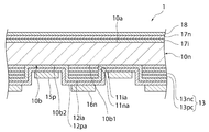
- FIG. 1 is a schematic cross-sectional view of a solar cell according to a first embodiment.
- the solar cell 1 has a substrate 10n made of a semiconductor material.
- the substrate 10n has n-type or p-type conductivity.
- the conductivity type of the substrate 10n is n-type.
- the substrate 10n can be made of, for example, an n-type crystalline semiconductor material.
- the substrate 10n can be composed of, for example, n-type crystalline silicon.
- the crystalline semiconductor material includes a single crystal semiconductor material and a polycrystalline semiconductor material. Crystalline silicon includes single crystal silicon and polycrystalline silicon.
- the substrate 10n has a first main surface 10a and a second main surface 10b that mainly receive light.
- the first main surface 10a is located on the light receiving surface side.
- the “light receiving surface” means a main surface on the side of mainly receiving light, out of the two main surfaces.
- a semiconductor layer 17i, a semiconductor layer 17n, and a protective layer 18 are provided in this order on the first main surface 10a.
- the semiconductor layer 17i is made of a substantially intrinsic i-type semiconductor material.
- the semiconductor layer 17i can be made of, for example, i-type amorphous silicon.
- the thickness of the semiconductor layer 17i is preferably a thickness that does not substantially contribute to power generation (for example, about 0.00 nm to 25 nm).
- the conductivity type of the semiconductor layer 17n is an n-type which is the same conductivity type as the substrate 10n.
- the semiconductor layer 17n can be made of, for example, n-type amorphous silicon.
- the protective layer 18 can be made of, for example, silicon nitride.
- the protective layer 18 may have a function of suppressing surface reflection of incident light as well as a function of protecting the semiconductor layer 17n.
- the amorphous semiconductor layer 11na is disposed on the first region 10b1 of the second main surface 10b.
- the amorphous semiconductor layer 11na has the same conductivity type as the substrate 10n.
- the conductivity type of the amorphous semiconductor layer 11na is n-type.
- the amorphous semiconductor layer 11na may have a conductivity type different from that of the substrate 10n.
- the amorphous semiconductor layer 11na can be made of n-type amorphous silicon, for example.
- a substantially intrinsic i-type amorphous semiconductor layer 11ia is provided between the first amorphous semiconductor layer 11na and the second main surface 10b.
- the i-type amorphous semiconductor layer 11ia has a thickness that does not substantially contribute to power generation (for example, about 0.00 nm to 25 nm).
- the i-type amorphous semiconductor layer 11ia can be made of, for example, i-type amorphous silicon.
- a substantially intrinsic i-type amorphous semiconductor layer 12ia is provided on the second region 10b2 which is at least a part of the region other than the first region 10b1 of the second main surface 10b.
- An amorphous semiconductor layer 12pa is provided on the i-type amorphous semiconductor layer 12ia.
- the amorphous semiconductor layer 12pa constitutes a second amorphous semiconductor layer and a third amorphous semiconductor layer.
- the i-type amorphous semiconductor layer 12ia and the amorphous semiconductor layer 12pa are provided across the second region 10b2 and the amorphous semiconductor layer 11na. Accordingly, the amorphous semiconductor layer 11na and the amorphous semiconductor layer 12pa are stacked in the first region 10b1.
- the i-type amorphous semiconductor layer 12ia can be composed of, for example, i-type amorphous silicon.
- the thickness of the i-type amorphous semiconductor layer 12ia is preferably a thickness that does not substantially contribute to power generation (for example, about 0.00 nm to 25 nm).
- the amorphous semiconductor layer 12pa has a conductivity type different from that of the substrate 10n. Specifically, the conductivity type of the amorphous semiconductor layer 12pa is p-type.
- the amorphous semiconductor layer 12pa can be composed of, for example, p-type amorphous silicon.
- a crystalline semiconductor layer 13 is provided between the amorphous semiconductor layer 11na and the i-type amorphous semiconductor layer 12ia.
- the crystalline semiconductor layer 13 is a layer that recombines holes and electrons.
- the crystalline semiconductor layer 13 has a defect level that can be a recombination center. For this reason, recombination of electrons and holes is likely to occur in the crystalline semiconductor layer 13. Therefore, a current flows through the crystalline semiconductor layer 13.
- the thickness of the crystalline semiconductor layer 13 is preferably about 2 nm to 60 nm, for example, and more preferably 2 nm to 30 nm.
- the crystal semiconductor layer 13 includes a first crystal semiconductor layer 13nc and a second crystal semiconductor layer 13pc.
- the first crystalline semiconductor layer 13nc is provided on the amorphous semiconductor layer 11na.
- the first crystalline semiconductor layer 13nc is in contact with the amorphous semiconductor layer 11na.
- the first crystalline semiconductor layer 13nc has the same conductivity type as the amorphous semiconductor layer 11na.
- the conductivity type of the first crystalline semiconductor layer 13nc is n-type.
- the first crystalline semiconductor layer 13nc can be composed of, for example, n-type microcrystalline silicon.
- the thickness of the first crystalline semiconductor layer 13nc is, for example, preferably about 1 nm to 30 nm, and more preferably 1 nm to 15 nm.
- the second crystal semiconductor layer 13pc is disposed between the first crystal semiconductor layer 13nc and the i-type amorphous semiconductor layer 12ia.
- the second crystal semiconductor layer 13pc is in contact with each of the first crystal semiconductor layer 13nc and the i-type amorphous semiconductor layer 12ia.
- the second crystal semiconductor layer 13pc has a conductivity type different from that of the first crystal semiconductor layer 13nc. Specifically, the conductivity type of the second crystalline semiconductor layer 13pc is p-type.
- the second crystalline semiconductor layer 13pc can be made of, for example, p-type microcrystalline silicon.
- the thickness of the second crystalline semiconductor layer 13pc is, for example, preferably about 1 nm to 30 nm, and more preferably 1 nm to 15 nm.
- microcrystalline semiconductor layer refers to a layer including a plurality of semiconductor crystal grains.
- the microcrystalline semiconductor layer includes a layer that substantially includes only semiconductor crystal grains.
- the microcrystalline semiconductor layer may include an amorphous region of a semiconductor in addition to the semiconductor crystal grains.
- an n-side electrode 16n is provided on the amorphous semiconductor layer 12pa.
- a p-side electrode 15p is provided on the amorphous semiconductor layer 12pa.
- the electrodes 15p and 16n can be made of at least one of metals such as Ag and Cu, for example.
- the first crystalline semiconductor layer 13nc having the same conductivity type as the amorphous semiconductor layer 11na is arranged between the amorphous semiconductor layer 11na and the i-type amorphous semiconductor layer 12ia. Also, between the first crystalline semiconductor layer 13nc and the i-type amorphous semiconductor layer 12ia.
- a second crystal semiconductor layer 13pc having a conductivity type different from that of the first crystal semiconductor layer 13nc is provided.
- the second crystalline semiconductor layer 13pc has the same conductivity type as the amorphous semiconductor layer 12pa.
- the first crystalline semiconductor layer 13nc having the same conductivity type as the amorphous semiconductor layer 11na and the second conductivity type having the same conductivity type as the amorphous semiconductor layer 12pa.
- a crystal semiconductor layer 13 which is a stacked body with the crystal semiconductor layer 13pc is arranged. For this reason, for example, as compared with the case where an amorphous semiconductor layer having the same conductivity type as that of the second amorphous semiconductor layer is provided between the first amorphous semiconductor layer and the i-type amorphous semiconductor layer, the photovoltaic cell of the solar cell is used. Conversion efficiency can be improved. The reason for this is considered to be that the effect of reducing the electrical resistance between the amorphous semiconductor layer 11na and the n-side electrode 16n is great.
- Example 1 of the present invention the electrical resistance between the substrate 10n and the second crystalline semiconductor layer 13pc in Example 1 of the present invention and the electrical resistance of other forms will be compared and examined.
- Example 1 A solar cell was fabricated in the same manner as in Example 1 except that a p-type amorphous silicon layer was provided instead of the first and second crystalline semiconductor layers 13nc and 13pc, and the substrate 10n and the p-type amorphous silicon layer The electrical resistance between was measured. The results are shown in Table 1 below.
- Example 2 A solar cell was fabricated in the same manner as in Example 1 except that a p-type amorphous silicon layer was provided instead of the second crystalline semiconductor layer 13pc, and the electric resistance between the substrate 10n and the p-type amorphous silicon layer was Was measured. The results are shown in Table 1 below.
- Example 3 A solar cell was fabricated in the same manner as in Example 1 except that the first crystal semiconductor layer 13nc was not provided, and the electrical resistance between the substrate 10n and the second crystal semiconductor layer 13pc was measured. The results are shown in Table 1 below.
Landscapes
- Photovoltaic Devices (AREA)
- Life Sciences & Earth Sciences (AREA)
- Engineering & Computer Science (AREA)
- Sustainable Energy (AREA)
Description
本発明は、改善された光電変換効率を有する太陽電池を提供することを主な目的とする。
図1に示されるように、太陽電池1は、半導体材料からなる基板10nを有する。基板10nは、n型またはp型の導電型を有する。本実施形態では、具体的には、基板10nの導電型は、n型である。基板10nは、例えば、n型の結晶半導体材料などにより構成することができる。具体的には、基板10nは、例えば、n型の結晶シリコンにより構成することができる。なお、結晶半導体材料には、単結晶半導体材料と多結晶半導体材料とが含まれるものとする。結晶シリコンには、単結晶シリコンと多結晶シリコンとが含まれるものとする。
第1及び第2の結晶半導体層13nc、13pcに代えて、p型アモルファスシリコン層を設けたこと以外は、実施例1と同様にして太陽電池を作製し、基板10nとp型アモルファスシリコン層との間の電気抵抗を測定した。結果を下記の表1に示す。
第2の結晶半導体層13pcに代えて、p型アモルファスシリコン層を設けたこと以外は、実施例1と同様にして太陽電池を作製し、基板10nとp型アモルファスシリコン層との間の電気抵抗を測定した。結果を下記の表1に示す。
第1の結晶半導体層13ncを設けなかったこと以外は、実施例1と同様にして太陽電池を作製し、基板10nと第2の結晶半導体層13pcとの間の電気抵抗を測定した。結果を下記の表1に示す。

10b1…第1の領域
10b…第2の主面
10b2…第2の領域
10n…半導体材料からなる基板
11ia、12ia…i型アモルファス半導体層
11na…アモルファス半導体層
12pa…アモルファス半導体層
13…結晶半導体層
13nc…第1の結晶半導体層
13pc…第2の結晶半導体層
15p…p側電極
16n…n側電極
Claims (3)
- 半導体材料からなる基板と、
前記基板の一領域の上に配されており、一の導電型を有する第1のアモルファス半導体層と、
前記基板の他の領域の上に配されており、他の導電型を有する第2のアモルファス半導体層と、
前記第1のアモルファス半導体層の上に設けられた実質的に真性なi型アモルファス半導体層と、
前記i型アモルファス半導体層の上に設けられており、他の導電型を有する第3のアモルファス半導体層と、
前記第1のアモルファス半導体層と前記i型アモルファス半導体層との間に配されており、前記一の導電型を有する第1の結晶半導体層と、
前記第1の結晶半導体層と前記i型アモルファス半導体層との間に配されており、前記他の導電型を有する第2の結晶半導体層と、
を備える、太陽電池。 - 前記第1の結晶質半導体及び前記第2の結晶質半導体は、微結晶半導体からなる、請求項1に記載の太陽電池。
- 前記一の導電型がn型であり、前記他の導電型がp型である、請求項1または2に記載の太陽電池。
Priority Applications (4)
| Application Number | Priority Date | Filing Date | Title |
|---|---|---|---|
| JP2014522326A JP5967555B2 (ja) | 2012-06-29 | 2012-06-29 | 太陽電池 |
| PCT/JP2012/066726 WO2014002257A1 (ja) | 2012-06-29 | 2012-06-29 | 太陽電池 |
| DE201211006595 DE112012006595T5 (de) | 2012-06-29 | 2012-06-29 | Solarzelle |
| US14/582,505 US9196780B2 (en) | 2012-06-29 | 2014-12-24 | Solar cell |
Applications Claiming Priority (1)
| Application Number | Priority Date | Filing Date | Title |
|---|---|---|---|
| PCT/JP2012/066726 WO2014002257A1 (ja) | 2012-06-29 | 2012-06-29 | 太陽電池 |
Related Child Applications (1)
| Application Number | Title | Priority Date | Filing Date |
|---|---|---|---|
| US14/582,505 Continuation US9196780B2 (en) | 2012-06-29 | 2014-12-24 | Solar cell |
Publications (1)
| Publication Number | Publication Date |
|---|---|
| WO2014002257A1 true WO2014002257A1 (ja) | 2014-01-03 |
Family
ID=49782481
Family Applications (1)
| Application Number | Title | Priority Date | Filing Date |
|---|---|---|---|
| PCT/JP2012/066726 Ceased WO2014002257A1 (ja) | 2012-06-29 | 2012-06-29 | 太陽電池 |
Country Status (4)
| Country | Link |
|---|---|
| US (1) | US9196780B2 (ja) |
| JP (1) | JP5967555B2 (ja) |
| DE (1) | DE112012006595T5 (ja) |
| WO (1) | WO2014002257A1 (ja) |
Families Citing this family (1)
| Publication number | Priority date | Publication date | Assignee | Title |
|---|---|---|---|---|
| US10217878B2 (en) | 2016-04-01 | 2019-02-26 | Sunpower Corporation | Tri-layer semiconductor stacks for patterning features on solar cells |
Citations (4)
| Publication number | Priority date | Publication date | Assignee | Title |
|---|---|---|---|---|
| JP2005101151A (ja) * | 2003-09-24 | 2005-04-14 | Sanyo Electric Co Ltd | 光起電力素子およびその製造方法 |
| JP2010153930A (ja) * | 2003-10-27 | 2010-07-08 | Mitsubishi Heavy Ind Ltd | 太陽電池及び太陽電池の製造方法 |
| WO2010098445A1 (ja) * | 2009-02-26 | 2010-09-02 | 三洋電機株式会社 | 太陽電池 |
| JP2011014619A (ja) * | 2009-06-30 | 2011-01-20 | Sanyo Electric Co Ltd | 太陽電池及びその製造方法 |
Family Cites Families (3)
| Publication number | Priority date | Publication date | Assignee | Title |
|---|---|---|---|---|
| EP2143144B1 (en) * | 2007-04-27 | 2018-11-28 | Merck Patent GmbH | Organic photovoltaic cells |
| JP5518347B2 (ja) * | 2009-02-26 | 2014-06-11 | 三洋電機株式会社 | 太陽電池の製造方法 |
| US8288645B2 (en) * | 2009-03-17 | 2012-10-16 | Sharp Laboratories Of America, Inc. | Single heterojunction back contact solar cell |
-
2012
- 2012-06-29 DE DE201211006595 patent/DE112012006595T5/de not_active Ceased
- 2012-06-29 WO PCT/JP2012/066726 patent/WO2014002257A1/ja not_active Ceased
- 2012-06-29 JP JP2014522326A patent/JP5967555B2/ja not_active Expired - Fee Related
-
2014
- 2014-12-24 US US14/582,505 patent/US9196780B2/en not_active Expired - Fee Related
Patent Citations (4)
| Publication number | Priority date | Publication date | Assignee | Title |
|---|---|---|---|---|
| JP2005101151A (ja) * | 2003-09-24 | 2005-04-14 | Sanyo Electric Co Ltd | 光起電力素子およびその製造方法 |
| JP2010153930A (ja) * | 2003-10-27 | 2010-07-08 | Mitsubishi Heavy Ind Ltd | 太陽電池及び太陽電池の製造方法 |
| WO2010098445A1 (ja) * | 2009-02-26 | 2010-09-02 | 三洋電機株式会社 | 太陽電池 |
| JP2011014619A (ja) * | 2009-06-30 | 2011-01-20 | Sanyo Electric Co Ltd | 太陽電池及びその製造方法 |
Also Published As
| Publication number | Publication date |
|---|---|
| JP5967555B2 (ja) | 2016-08-10 |
| US20150114465A1 (en) | 2015-04-30 |
| JPWO2014002257A1 (ja) | 2016-05-30 |
| DE112012006595T5 (de) | 2015-04-02 |
| US9196780B2 (en) | 2015-11-24 |
Similar Documents
| Publication | Publication Date | Title |
|---|---|---|
| JP5461028B2 (ja) | 太陽電池 | |
| JP5538360B2 (ja) | 太陽電池の製造方法及び太陽電池 | |
| JP5518347B2 (ja) | 太陽電池の製造方法 | |
| JP6452011B2 (ja) | 太陽電池 | |
| JPWO2009110403A1 (ja) | 光電変換素子構造及び太陽電池 | |
| JP6414767B2 (ja) | 太陽電池セル | |
| JPWO2012132835A1 (ja) | 太陽電池 | |
| JP6706779B2 (ja) | 太陽電池および太陽電池モジュール | |
| TWI506801B (zh) | 太陽能電池組 | |
| US20120180861A1 (en) | Solar cell | |
| JP5967555B2 (ja) | 太陽電池 | |
| JP5971499B2 (ja) | 太陽電池及びその製造方法 | |
| JP6083539B2 (ja) | 太陽電池 | |
| JP4436770B2 (ja) | 光起電力装置 | |
| JP5950136B2 (ja) | 太陽電池 | |
| CN102163629B (zh) | 太阳能电池 | |
| JP6380822B2 (ja) | 太陽電池セル | |
| JP5963024B2 (ja) | 太陽電池の製造方法及び太陽電池 | |
| JP5816800B2 (ja) | 太陽電池の製造方法 | |
| CN103165718B (zh) | 太阳能电池组 | |
| JP2013074277A (ja) | 光電変換装置 |
Legal Events
| Date | Code | Title | Description |
|---|---|---|---|
| 121 | Ep: the epo has been informed by wipo that ep was designated in this application |
Ref document number: 12879727 Country of ref document: EP Kind code of ref document: A1 |
|
| ENP | Entry into the national phase |
Ref document number: 2014522326 Country of ref document: JP Kind code of ref document: A |
|
| WWE | Wipo information: entry into national phase |
Ref document number: 112012006595 Country of ref document: DE Ref document number: 1120120065956 Country of ref document: DE |
|
| 122 | Ep: pct application non-entry in european phase |
Ref document number: 12879727 Country of ref document: EP Kind code of ref document: A1 |