WO2013175865A1 - Capteur de courant - Google Patents
Capteur de courant Download PDFInfo
- Publication number
- WO2013175865A1 WO2013175865A1 PCT/JP2013/059609 JP2013059609W WO2013175865A1 WO 2013175865 A1 WO2013175865 A1 WO 2013175865A1 JP 2013059609 W JP2013059609 W JP 2013059609W WO 2013175865 A1 WO2013175865 A1 WO 2013175865A1
- Authority
- WO
- WIPO (PCT)
- Prior art keywords
- magnetic
- current sensor
- magnetic core
- core
- hall
- Prior art date
Links
Images


Classifications
-
- G—PHYSICS
- G01—MEASURING; TESTING
- G01R—MEASURING ELECTRIC VARIABLES; MEASURING MAGNETIC VARIABLES
- G01R15/00—Details of measuring arrangements of the types provided for in groups G01R17/00 - G01R29/00, G01R33/00 - G01R33/26 or G01R35/00
- G01R15/14—Adaptations providing voltage or current isolation, e.g. for high-voltage or high-current networks
- G01R15/20—Adaptations providing voltage or current isolation, e.g. for high-voltage or high-current networks using galvano-magnetic devices, e.g. Hall-effect devices, i.e. measuring a magnetic field via the interaction between a current and a magnetic field, e.g. magneto resistive or Hall effect devices
- G01R15/202—Adaptations providing voltage or current isolation, e.g. for high-voltage or high-current networks using galvano-magnetic devices, e.g. Hall-effect devices, i.e. measuring a magnetic field via the interaction between a current and a magnetic field, e.g. magneto resistive or Hall effect devices using Hall-effect devices
-
- G—PHYSICS
- G01—MEASURING; TESTING
- G01R—MEASURING ELECTRIC VARIABLES; MEASURING MAGNETIC VARIABLES
- G01R19/00—Arrangements for measuring currents or voltages or for indicating presence or sign thereof
- G01R19/0092—Arrangements for measuring currents or voltages or for indicating presence or sign thereof measuring current only
-
- G—PHYSICS
- G01—MEASURING; TESTING
- G01R—MEASURING ELECTRIC VARIABLES; MEASURING MAGNETIC VARIABLES
- G01R15/00—Details of measuring arrangements of the types provided for in groups G01R17/00 - G01R29/00, G01R33/00 - G01R33/26 or G01R35/00
- G01R15/14—Adaptations providing voltage or current isolation, e.g. for high-voltage or high-current networks
- G01R15/20—Adaptations providing voltage or current isolation, e.g. for high-voltage or high-current networks using galvano-magnetic devices, e.g. Hall-effect devices, i.e. measuring a magnetic field via the interaction between a current and a magnetic field, e.g. magneto resistive or Hall effect devices
- G01R15/207—Constructional details independent of the type of device used
-
- G—PHYSICS
- G01—MEASURING; TESTING
- G01R—MEASURING ELECTRIC VARIABLES; MEASURING MAGNETIC VARIABLES
- G01R33/00—Arrangements or instruments for measuring magnetic variables
- G01R33/02—Measuring direction or magnitude of magnetic fields or magnetic flux
- G01R33/06—Measuring direction or magnitude of magnetic fields or magnetic flux using galvano-magnetic devices
- G01R33/07—Hall effect devices
- G01R33/072—Constructional adaptation of the sensor to specific applications
Definitions
- the present invention relates to a magnetic proportional type or magnetic balance type current sensor used for current measurement and detection.
- Patent Document 1 is an example of prior art relating to a magnetic proportional current detector.
- the current detector according to the fifth embodiment of Patent Document 1 will be described with reference to FIG.
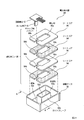
- FIG. 21 is an exploded perspective view showing the current sensor according to the fifth embodiment of Patent Document 1 as components.
- the current detector 90 includes a resin case 92, and a plurality of plate-like sheet cores 94 and 96 are accommodated in the resin case 92 so as to overlap each other. These sheet cores 94 and 96 constitute one magnetic core 98 while being accommodated in the resin case 92. Although two sheet cores 94 and 96 are shown in FIG. 21, the actual number is larger than this, and they are not shown.
- Each of the sheet cores 94 and 96 has a substantially square C shape, and the sheet cores 94 and 96 having such a shape are formed by punching a plate-shaped magnetic material. At that time, each of the sheet cores 94 and 96 is formed with openings 94a and 96a at the center thereof, and gap slits 94b and 96b extending from the openings 94a and 96a toward one side edge.
- the openings 94 a and 96 a are substantially square shapes that match the outer shape of the seat cores 94 and 96.
- the openings 94a and 96a and the gap slits 94b and 96b match each other when viewed in the overlapping direction.
- a continuous through hole is formed at the center position, and a core gap is formed in a part in the circumferential direction. It will be.
- an accommodating portion 92a and a guide sleeve 92b are formed.
- the accommodation portion 92a is open at the top shown in FIG. 21, but a bottom plate 92c is formed below the accommodation portion 92a.
- the guide sleeve 92b extends upward from the bottom plate 92c, and the inside thereof is formed as a hollow current conducting portion 92d.
- the outer shape of the guide sleeve 92b is slightly smaller than the openings 94a and 96a of the seat cores 94 and 96, and the inner dimension of the accommodating portion 92a is larger than the outer shape of the seat cores 94 and 96.
- the openings 94a and 96a are guided along the outer surface of the guide sleeve 92b, so that the seat cores 94 and 96 can be easily positioned relative to each other. It has been done.
- the resin case 92 accommodates the Hall element 10 together with the sheet cores 94 and 96.
- the Hall element 10 is mounted on a circuit board 12, and the circuit board 12 is accommodated so as to be superimposed on the upper surface of the outermost sheet core 96. At this time, the Hall element 10 is positioned in the core gap of the magnetic core 98 by being inserted between the gap slits 94b and 96b of the respective sheet cores 94 and 96.
- the sheet core 96 is a non-oriented silicon steel plate and has a portion (particularly hysteresis width) inferior in magnetic properties as a current detection core, but another sheet core 94 is a permalloy, and is used as a current detection core. Excellent magnetic characteristics (output linearity, hysteresis width, saturation characteristics).
- the magnetic core 98 By forming the magnetic cores 98 by superimposing the sheet cores 94 and 96 made of different magnetic materials on each other, defects inherent to the sheet core 96 can be compensated for by another sheet core 94. As a result, the magnetic core 98 as a whole can exhibit good magnetic characteristics, and can exhibit sufficient characteristics as a product.
- the non-oriented silicon steel plate which is a relatively inexpensive magnetic material
- permalloy which is a relatively expensive magnetic material
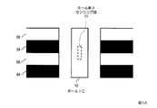
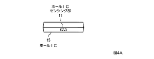
- FIG. 1 is a diagram schematically showing a problem of a current detector using a magnetic core formed by laminating a plurality of conventional materials.
- FIG. 1A is a schematic diagram of the AA cross section in FIG. 21 in a state in which the Hall element 10 is inserted into the core gap of the magnetic core 98.
- FIG. 1B is a schematic diagram for explaining the variation in the total number of magnetic fluxes penetrating through the Hall element sensing unit 11 caused by the position variation of the Hall element sensing unit 11 and the position variation. As shown by a broken line in FIG.
- a Hall element sensing unit 11 that is a region for detecting a magnetic field generated from the magnetic core 98 exists in the Hall element 10.
- the Hall element 10 including the Hall element sensing unit 11 is roughly positioned when the circuit board 12 is accommodated in the accommodating portion 92 a and placed on the uppermost sheet core of the magnetic core 98.
- the inside of the housing portion 92a of the resin case 92 is sealed with a potting resin (not shown).
- the position of the Hall element sensing unit 11 may vary in position as compared with the product as shown by the broken line in FIG. 1B.
- the sheet cores 94 and 96 are made of materials having different magnetic permeability, even if the currents to be measured are equal, the total number of magnetic fluxes penetrating the sensing unit 11 varies between products, and the sensitivity of the current sensor is increased. There was a problem that an error would occur. Further, not only the position variation among products but also the position of the sensing unit 11 may fluctuate due to vibrations applied to the current sensor body during use, thereby changing the sensitivity of the current sensor.
- an object of the present invention is to provide a current sensor that can suppress fluctuations in sensitivity due to variations in the position of a Hall element even when a magnetic core formed by laminating a plurality of materials is used.
- the current sensor of the present invention includes a magnetic core formed in an annular shape with a gap at a part of the circumference, and a magnetic flux that is arranged in the gap and changes according to a current to be measured that passes through a hollow portion of the magnetic core. And a magnetoelectric conversion element for detecting.
- a magnetic core is formed by laminating a plurality of materials in a direction other than the circumferential direction, and is laminated in a region (hereinafter referred to as a sensing unit existence region) predetermined as a region where a sensing unit of a magnetoelectric conversion element can exist. It is characterized in that it is formed so that the magnetic flux density at two points whose direction distances are separated by the length in the stacking direction of the sensing unit is approximate.
- the above-described magnetic core may be formed by irregularly laminating a plurality of materials.
- the above-mentioned magnetic cores may be formed by concentrically laminating.
- the above-described magnetic core may be formed by being laminated in the conduction direction of the current to be measured.
- the above-described magnetic core may be formed by rounding a flat plate in which a plurality of different materials are laminated, and cutting a part of the circumference.
- the magnetic core described above may be formed by alternately laminating directional electromagnetic steel and amorphous magnetic alloy.
- the magnetic core described above may be formed by alternately laminating directional electromagnetic steel and ferrite.
- the perspective view of the magnetic body core with which the current sensor which concerns on the Example of this invention is provided.
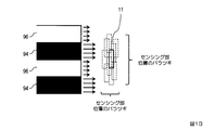
- the figure (top view) which shows typically the positional relationship of the magnetic body core with which the current sensor which concerns on the Example of this invention is provided, and a Hall IC sensing part.
- the figure (front view) which shows typically the positional relationship of the magnetic body core with which the current sensor which concerns on the Example of this invention is provided, and a Hall IC sensing part.
- the figure which shows typically the variation in the position of the Hall IC sensing part with which the current sensor which concerns on the Example of this invention is provided.
- FIG. The figure which shows typically the characteristic of magnetic flux density distribution in the gap of the current sensor of Example 2.
- FIG. 3 is a schematic diagram illustrating an application example 1 that can be employed in the current sensor according to the first embodiment.
- FIG. 3 is a schematic diagram illustrating an application example 2 that can be employed in the current sensor according to the first embodiment.
- FIG. 6 is a schematic diagram illustrating an application example 3 that can be employed in the current sensor according to the first embodiment.
- FIG. 6 is a schematic diagram illustrating an application example 4 that can be employed in the current sensor according to the first embodiment.
- FIG. 6 is a schematic diagram illustrating an application example 5 that can be employed in the current sensor according to the first embodiment.
- FIG. 6 is a schematic diagram illustrating an application example 6 that can be employed in the current sensor according to the first embodiment.
- FIG. 6 is a schematic diagram illustrating an application example 7 that can be employed in the current sensor according to the first embodiment.
- FIG. 6 is a schematic diagram showing an application example 8 that can be employed in the current sensor of the first embodiment.
- FIG. 6 is a schematic diagram illustrating an application example 9 that can be employed in the current sensor according to the first embodiment.
- FIG. 10 is a schematic diagram illustrating an application example 10 that can be employed in the current sensor according to the second embodiment.
- FIG. 10 is a schematic diagram illustrating an application example 11 that can be employed in the current sensor according to the second embodiment.
- FIG. 10 is a schematic diagram illustrating an application example 12 that can be employed in the current sensor according to the second embodiment.
- FIG. 10 is a schematic diagram illustrating an application example 13 that can be employed in the current sensor according to the second embodiment.
- FIG. 10 is a schematic diagram showing an application example 14 that can be employed in the current sensor according to the second embodiment.
- FIG. 10 is a schematic diagram illustrating an application example 15 that can be employed in the current sensor according to the second embodiment.
- FIG. 9 is a schematic diagram illustrating an application example 16 that can be employed in the current sensor according to the second embodiment.
- FIG. 9 is a schematic diagram illustrating an application example 17 that can be employed in the current sensor according to the second embodiment.
- FIG. 10 is a schematic diagram illustrating an application example 12 that can be employed in the current sensor according to the second embodiment.
- FIG. 10 is a schematic diagram illustrating an application example 13 that can be employed in the current sensor according to the second embodiment.
- FIG. 10 is a schematic diagram showing an application example 14 that can
- FIG. 10 is a schematic diagram illustrating an application example 18 that can be employed in the current sensor according to the second embodiment.
- FIG. 10 is a schematic diagram illustrating an application example 19 that can be employed in the current sensor according to the third embodiment.
- FIG. 10 is a schematic diagram illustrating an application example 20 that can be employed in the current sensor according to the third embodiment.
- FIG. 10 is a schematic diagram showing an application example 21 that can be employed in the current sensor of the third embodiment.
- FIG. 14 is a schematic diagram showing an application example 22 that can be employed in the current sensor according to the third embodiment.
- FIG. 14 is a schematic diagram showing an application example 23 that can be employed in the current sensor of the third embodiment.
- FIG. 10 is a schematic diagram illustrating an application example 24 that can be employed in the current sensor according to the third embodiment.
- the perspective view shown about the example of the magnetic core which the shape of the magnetic body with which the current sensor of this invention is provided, and the shape which is the variation of the lamination direction were made into the substantially square C shape, and were laminated
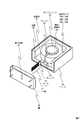
- FIG. 2 is an exploded perspective view of main components of the current sensor according to the embodiment of the present invention.
- FIG. 3 is a perspective view of a magnetic core provided in the current sensor according to the embodiment of the present invention.
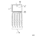
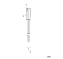
- 4A and 4B are three views of the Hall IC included in the current sensor according to the embodiment of the present invention.
- FIG. 4A is a plan view
- FIG. 4B is a front view
- FIG. 4C is a right side view.
- a current sensor is a device that detects a current flowing in a bus bar or a cable that electrically connects a battery and a device such as a motor in a vehicle such as an electric vehicle or a hybrid vehicle.
- the current sensor according to the embodiment of the present invention includes a magnetic core 100 (101 to 108, 200 to 208, 300 to 305, the reference numeral is properly used for each embodiment described later), a Hall IC 15, A lead wire 13 connected to the Hall IC 15, a case 50, and a lid 60 are provided.
- the magnetic core 100 (101 to 108, 200 to 208, 300 to 305) of the present invention is a soft magnetic material (a material having a small coercive force and a high magnetic permeability, such as iron, silicon steel, permalloy, sendust, permendur, Soft ferrite, amorphous magnetic alloy, nanocrystal magnetic alloy, electromagnetic steel, etc.).
- the electromagnetic steel there are a non-oriented steel plate that is not magnetized by being biased in a specific direction, and a directional steel plate that is easily magnetized only in a specific direction.
- the stacking direction of the plurality of materials may be any direction as long as it is a direction other than the circumferential direction of the core.
- the kind of material may be two kinds, may be three kinds, and may be any kind as long as it is two or more kinds.
- the plurality of materials may be laminated irregularly. Details will be described later.
- the Hall IC 15 provided in the current sensor of the present invention changes according to the current to be measured flowing through the bus bar or cable inserted through the hollow portion 30 of the magnetic core 100 (101 to 108, 200 to 208, 300 to 305).
- the magnetic flux to be detected is detected, and the magnetic flux detection signal is output as an electric signal.
- the Hall IC 15 is connected to an external circuit (not shown) via the lead wire 13.
- the Hall IC 15 may be realized by a combination of a Hall element and an electric circuit.
- the Hall IC 15 and the Hall element are examples of a magnetoelectric conversion element.
- the case 50 has a rectangular parallelepiped box shape, and an upper surface and one side surface are open.
- a cylindrical guide sleeve 52 is provided so as to penetrate the bottom surface 55 of the case 50, and a bus bar or a cable (not shown) can be inserted into the inner cavity (current conducting portion 54) of the guide sleeve 52.
- a stopper 53 that is a plate-like convex portion perpendicular to the outer surface is formed on the outer surface of the guide sleeve 52 adjacent to the opening on the side surface of the case 50.
- a region surrounded by the inner wall of the case 50 and the outer surface of the guide sleeve 52 is referred to as an accommodating portion 51. As shown in FIG.
- the magnetic core 100 (101 to 108, 200 to 208, 300 to 305) has a gap 20 at a part of its circumference and is formed in an annular shape.
- the magnetic core 100 (101 to 108, 200 to 208, 300 to 305) is formed by rounding a plate-like material in an annular shape in the longitudinal direction so as to surround the hollow portion 30, and both ends in the longitudinal direction are interposed via the gap 20. Opposite.
- the outer shape of the guide sleeve 52 is slightly smaller than the hollow part 30 of the magnetic core 100 (101 to 108, 200 to 208, 300 to 305).
- the width of the stopper 53 in the circumferential direction of the guide sleeve 52 is slightly smaller than the width of the gap 20 in the circumferential direction of the core.
- the inner dimension of the accommodating portion 51 is larger than the outer shape of the magnetic core 100 (101 to 108, 200 to 208, 300 to 305). Therefore, when the magnetic core 100 (101 to 108, 200 to 208, 300 to 305) is accommodated in the case 50, the hollow portion 30 and the gap 20 are guided along the outer surfaces of the guide sleeve 52 and the stopper 53.
- the magnetic core 100 (101 to 108, 200 to 208, 300 to 305) is roughly positioned by being placed on the bottom surface 55.
- the Hall IC 15 includes a rectangular parallelepiped case 15b, a magnetoelectric conversion circuit board (not shown) in the case 15b, and a Hall IC sensing unit 11 (the approximate position is indicated by a broken line).
- Five lead wires 13 (13 a, 13 b, 13 c, 13 d, 13 e) are provided at the lower end of the Hall IC 15, and the lead wire 13 is passed through a lead wire hole provided in the oval recess 61 of the lid 60. .
- the central lead wire 13c is provided with a flange portion 13c-1 in which a part of the lead wire 13c is thickened in a hook shape.
- the Hall IC 15 is held with respect to the lid 60 by catching the lead wire hole.
- the lid 60 is attached to the side opening of the case 50. At this time, the end 15a opposite to the end provided with the lead wire 13 of the Hall IC 15 contacts the stopper 53 and is roughly positioned.
- FIG. 5 is a diagram (plan view) schematically showing a positional relationship between the magnetic core and the Hall IC sensing unit provided in the current sensor according to the embodiment of the present invention.
- FIG. 6 is a diagram (front view) schematically illustrating the positional relationship between the magnetic core and the Hall IC sensing unit included in the current sensor according to the embodiment of the present invention. As shown in FIG.
- the end of the Hall IC sensing unit 11 in the core outer edge direction is referred to as an outer edge direction end 11a
- the end of the Hall IC sensing unit 11 in the core center direction is referred to as a center direction end 11b. I will do it.
- the end of the Hall IC sensing unit 11 in the core upper surface direction is referred to as an upper end 11c
- the end of the Hall IC sensing unit 11 in the core lower surface direction is the lower end 11d. I will call it.
- the positional variation of the Hall IC sensing unit 11 will be described with reference to FIG. As shown in FIG. 7, there is a possibility that the Hall IC sensing unit 11 may vary in position due to the addition of vibrations between products or in use in the core outer edge-center direction and in the core upper surface-lower surface direction. . This is the same as in the case of Patent Document 1.
- a region estimated to be the maximum as the position variation of the Hall IC sensing unit 11 is defined in advance as a sensing unit existence region.
- the sensing unit existence area includes a design value of play generated between the case 50 and the magnetic core 100 (101 to 108, 200 to 208, 300 to 305), a design value of play generated between the lid 60 and the case 50, You may estimate by calculating the largest play which can be theoretically generated from the design value of the play which arises between the lid
- the sensing unit existence region may be set with a margin as a region where the Hall IC sensing unit 11 exists reliably.
- the length in the stacking direction of the sensing portion existence region is represented as S, and is used as a parameter when determining the magnetic flux density distribution of the magnetic core described later.
- the lamination direction of the magnetic core of the present invention may be any direction as long as it is a direction other than the circumferential direction of the core.
- the stacking direction is the core outer edge-center direction. Therefore, in this case, the length S in the stacking direction of the sensing unit existing region is the maximum deviation position in the outer edge direction of the outer edge direction end 11a of the Hall IC sensing unit 11 and the central direction of the center direction end 11b of the Hall IC sensing unit 11 It is determined based on the maximum deviation position.
- the laminating direction is the core upper surface-lower surface direction. Therefore, in this case, the length S in the stacking direction of the sensing unit existence region is the maximum displacement position in the upper direction of the upper end 11c of the Hall IC sensing unit 11 and the lower direction of the lower end 11d of the Hall IC sensing unit 11 It is determined based on the maximum deviation position.
- FIG. 8 is a diagram schematically illustrating the characteristics of the magnetic flux density distribution in the gap of the current sensor according to the first embodiment.
- FIG. 9 is a diagram schematically illustrating the characteristics of the magnetic flux density distribution in the gap of the current sensor according to the second embodiment.
- the coordinates in the stacking direction of the outer edge direction maximum deviation position of the outer edge direction end portion 11a are referred to as EE.
- the coordinate in the stacking direction of the center direction maximum deviation position of the outer edge direction end portion 11a is referred to as EC.
- the coordinates in the stacking direction of the outer edge direction maximum deviation position of the center direction end portion 11b are referred to as CE.
- the coordinate in the stacking direction of the center direction maximum deviation position of the center direction end portion 11b is referred to as CC.
- the coordinate in the stacking direction of the maximum upward shift position of the upper end 11c is referred to as EE.
- the coordinate in the stacking direction of the downward maximum displacement position of the upper end portion 11c is referred to as EC.
- the coordinates in the stacking direction of the upward maximum shift position of the lower end portion 11d are referred to as CE.
- the coordinate in the stacking direction of the downward maximum displacement position of the downward end 11d is referred to as CC.
- the coordinates EE, EC, CE, and CC are used in the same definition in FIG.
- the magnetic flux generated near the right side of the coordinates CE newly penetrates the Hall IC sensing unit 11. Therefore, when the total number of magnetic fluxes penetrating the Hall IC sensing unit 11 is to be kept constant, the magnetic flux density at the coordinates at which the movement of the Hall IC sensing unit 11 does not affect the Hall IC sensing unit 11 and the movement are newly added. It suffices if the magnetic flux density at the coordinates that affect the Hall IC sensing unit 11 is approximate. Specifically, the magnetic flux densities in the vicinity of the coordinates EE and the coordinates CE need only be approximate. Similarly, the magnetic flux densities in the vicinity of the coordinates EC and the coordinates CC need only be approximate. These both corresponding coordinates are spaced a distance L H.
- the section from the left end of the core to the coordinate EE and the section from the coordinate CC to the right end of the core in the figure that do not affect the Hall IC sensing section 11 affects the total number of magnetic fluxes penetrating the Hall IC sensing section 11. No conditions are imposed.
- the magnetic flux generated near the coordinates CE newly penetrates the Hall IC sensing unit 11. Therefore, when the total number of magnetic fluxes penetrating the Hall IC sensing unit 11 is to be kept constant, the magnetic flux density at the coordinates at which the movement of the Hall IC sensing unit 11 does not affect the Hall IC sensing unit 11 and the movement are newly added. It suffices if the magnetic flux density at the coordinates that affect the Hall IC sensing unit 11 is approximate. Specifically, the magnetic flux densities in the vicinity of the coordinates EE and the coordinates CE need only be approximate. These both corresponding coordinates are spaced a distance L H. Up to this point, the process is the same as in FIG. However, in the case of FIG. 9, there is no region where the condition between the coordinates EC and CE existing in FIG. 8 is not imposed.
- section from the left end of the core to the coordinate EE and the section from the coordinate CC to the right end of the core in the figure that do not affect the Hall IC sensing section 11 affects the total number of magnetic fluxes penetrating the Hall IC sensing section 11. No conditions are imposed. This is the same as in FIG.
- the conditions to be satisfied by the magnetic cores 200 to 208 of the current sensor according to the second embodiment described in FIG. 9 are summarized again.
- the magnetic core 200 from 208 of the current sensor of Example 2 with the proviso that the magnetic flux density of the two-point distance in the stacking direction spaced apart by L H in the sensing part presence region is formed so as to approximate.
- the superordinate concept of the present invention described with reference to FIGS. 8 and 9 stipulates that the magnetic flux density at any two points in the region separated by L H is only approximate, and therefore, for example, the coordinate EE in FIG.
- the magnetic flux density distribution in the CC section may be irregular distribution.
- the magnetic flux density distribution from the coordinate EE to the CE section in FIG. 9 may be an irregular distribution.
- FIG. 10 is a schematic diagram schematically showing the regularity of the magnetic flux density distribution of the magnetic core included in the current sensor of the first embodiment.
- FIG. 11 is a diagram schematically illustrating the regularity of the magnetic flux density distribution of the magnetic core included in the current sensor according to the second embodiment.
- the relationship mutually compensating each other by the magnetic flux density of any two points exist in regions spaced L H approximates to suppress the variation in the sensitivity of the current sensor be able to.
- the compensation relationship is established.
- FIG. 12 is a schematic diagram illustrating an application example that can be employed in the current sensor according to the first embodiment.
- 12A is a schematic diagram illustrating the configuration of the magnetic core 100 of Application Example 1
- FIG. 12B is a schematic diagram illustrating the configuration of the magnetic core 101 of Application Example 2
- FIG. 12C illustrates the configuration of the magnetic core 102 of Application Example 3. It is a schematic diagram shown.
- the magnetic core 100 As an application example in which the magnetic core 100 is modified, a material different from the first magnetic body 1 and the second magnetic body 2 (fourth magnetic body) in the section between the coordinates EC and CE, as in the magnetic core 101 of this application example. 4).
- the magnetic core is formed of three kinds of magnetic bodies.
- the section from the left end of the core to the coordinate EE, the section from the coordinate CC to the right end of the core in the figure, and the section from the coordinates EC to CE are formed by laminating a plurality of types of magnetic materials. May be.
- FIG. 13 is a schematic diagram illustrating an application example that can be employed in the current sensor according to the first embodiment.
- 13A is a schematic diagram illustrating the configuration of the magnetic core 103 of Application Example 4
- FIG. 13B is a schematic diagram illustrating the configuration of the magnetic core 104 of Application Example 5
- FIG. 13C illustrates the configuration of the magnetic core 105 of Application Example 6. It is a schematic diagram shown.
- L H spaced magnetic flux density of any two points exist in regions becomes a condition that the approximate not impose any condition from the coordinate EC in magnetic flux density between the CE. Therefore, for example, two kinds of magnetic materials are arranged in an arbitrary pattern between EE and EC, and two kinds of magnetic materials used between EE and EC are arranged between CE and CC. Magnetic materials may be formed by arranging them in the same pattern. As shown in FIG. 13A, in the magnetic core 103 of this application example, the first magnetic body 1 and the third magnetic body 3 are alternately arranged in the sections from the coordinates EE to EC and CE to CC so that the same magnetic flux is obtained. A density distribution is formed.
- this section may have any configuration, such as a magnetic material, a non-magnetic material, and a plurality of types of magnetic materials laminated as in the first to third application examples.
- the first magnetic body 1 and the third magnetic body 3 are alternately arranged in the sections from the coordinates EE to EC and CE to CC, and the same magnetic flux density distribution is formed.
- This is the same as Application Example 4 in that the thicknesses of the first magnetic body 1 and the third magnetic body 3 are different. Specifically, the third magnetic body 3 was formed thinner than the layer of the first magnetic body 1.
- the magnetic core 105 of this application example is formed by alternately arranging two kinds of materials in the section from the coordinates EE to EC and CE to CC, as in the application examples 4 and 5.
- the magnetic core 105 of this application example is formed by alternately laminating magnetic bodies (in the figure, the third magnetic body 3 is shown, but there is no particular limitation on the type of magnetic body) and nonmagnetic bodies 9.
- the magnetic core can also be formed by laminating in an arbitrary pattern using the magnetic material and the non-magnetic material in the sections from the coordinates EE to EC and CE to CC.
- FIG. 14 is a schematic diagram illustrating an application example that can be employed in the current sensor according to the first embodiment.
- 14A is a schematic diagram illustrating the configuration of the magnetic core 106 of Application Example 7
- FIG. 14B is a schematic diagram illustrating the configuration of the magnetic core 107 of Application Example 8
- FIG. 14C illustrates the configuration of the magnetic core 108 of Application Example 9. It is a schematic diagram shown.
- the first magnetic body 1, the second magnetic body 2, and the third magnetic body 3 are arranged in the section from the coordinates EE to EC and CE to CC. , The same magnetic flux density distribution is formed.
- the first magnetic body 1 is formed thicker than the other layers.
- the magnetic core 108 of this application example has four types of magnetic bodies (first magnetic body 1, second magnetic body 2, third magnetic body 3, and fourth magnetic body in the sections from coordinates EE to EC and CE to CC. 4) are arranged to form the same magnetic flux density distribution.
- the application example 7 to the application example 9 show the magnetic core formed by irregularly arranging a plurality of types of magnetic bodies.
- the magnetic core is formed by regularly arranging the magnetic cores. It goes without saying that it is possible. In this case, as described with reference to FIG.
- the fluctuation of the current sensor sensitivity due to the position variation when the Hall IC 15 is disposed in the gap 20 is suppressed. Therefore, it is possible to realize a more accurate current sensor by suppressing variation between products (between operations).
- electromagnetic steel sheets have the disadvantage that high frequency currents of 10 kHz or higher cannot be measured due to iron loss such as eddy current loss, but by forming a magnetic core by combining electromagnetic steel sheets and materials with good frequency characteristics. A current sensor with improved frequency characteristics can be realized.
- ferrite has a demerit that the saturation magnetic flux density is small and the sensor sensitivity is lowered in a large current region, but a magnetic core is formed by laminating ferrite and a directional electrical steel sheet having a high saturation magnetic flux density.
- a current sensor with improved sensitivity in a large current region can be realized.
- Amorphous magnetic alloys have good properties as soft magnetic materials, but have the disadvantage of low mechanical strength, but form a magnetic core by laminating amorphous magnetic alloys and directional electrical steel sheets with high mechanical strength. By doing so, a magnetic core and a current sensor with high mechanical strength can be realized.
- FIG. 15 is a schematic diagram illustrating an application example that can be employed in the current sensor according to the second embodiment.
- 15A is a schematic diagram illustrating the configuration of the magnetic core 200 of Application Example 10
- FIG. 15B is a schematic diagram illustrating the configuration of the magnetic core 201 of Application Example 11
- FIG. 15C illustrates the configuration of the magnetic core 202 of Application Example 12. It is a schematic diagram shown.
- the magnetic flux density of any two points exist in regions spaced L H is that it is the conditions are similar, for example, for inter-CC from the coordinate EE, the magnetic flux density is flat distribution In this way, it is sufficient to configure only one type of magnetic body (first magnetic body 1). Since no condition is imposed on the section of the magnetic core 200 from the left end of the core in the drawing to the coordinate EE, and the section from the coordinate CC to the right end of the core in the drawing, for example, a second magnet different from the first magnetic body 1 is used. A layer of the body 2 may be formed.
- the magnetic core 200 As an application example in which the magnetic core 200 is deformed, a material different from the first magnetic body 1 and the second magnetic body 2 in the section from the coordinate CC to the right end of the core in the figure as in the magnetic core 201 of this application example (The fourth magnetic body 4 may be used.
- the magnetic core is formed of three kinds of magnetic bodies.
- the section from the left end of the core to the coordinate EE and the section from the coordinate CC to the right end of the core in the figure are not magnetic bodies.
- You may comprise a substance (nonmagnetic material 9).
- the section from the core left end in the figure to the coordinate EE and the section from the coordinate CC to the core right end in the figure may be configured by laminating a plurality of types of magnetic materials.
- FIG. 16 is a schematic diagram illustrating an application example that can be employed in the current sensor according to the second embodiment.
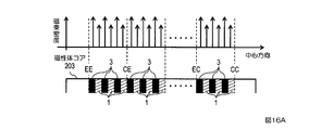
- 16A is a schematic diagram showing the configuration of the magnetic core 203 of the application example 13
- FIG. 16B is a schematic diagram showing the configuration of the magnetic core 204 of the application example 14
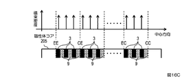
- FIG. 16C shows the configuration of the magnetic core 205 of the application example 15. It is a schematic diagram shown.
- any structure such as a magnetic body, a non-magnetic body, and a stack of a plurality of types of magnetic bodies may be used.
- the thicknesses of the first magnetic body 1 and the third magnetic body 3 are made different from each other.
- the third magnetic body 3 was formed thinner than the layer of the first magnetic body 1.
- the magnetic core 205 of this application example is formed by alternately laminating magnetic bodies (in the figure, the third magnetic body 3 is shown, but there is no particular limitation on the type of magnetic body) and nonmagnetic bodies 9.
- FIG. 17 is a schematic diagram illustrating an application example that can be employed in the current sensor according to the second embodiment.
- 17A is a schematic diagram showing the configuration of the magnetic core 206 of Application Example 16
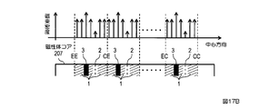
- FIG. 17B is a schematic diagram showing the configuration of the magnetic core 207 of Application Example 17
- FIG. 17C shows the configuration of the magnetic core 208 of Application Example 18. It is a schematic diagram shown.
- the first magnetic body 1 is formed thicker than the other layers.
- the variation in the current sensor products (between operations) is suppressed, and a more accurate current sensor is realized. It is possible to supplement the disadvantages of each material and enjoy the advantages of each material.
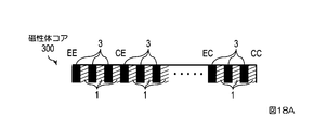
- FIG. 18 is a schematic diagram illustrating an application example that can be employed in the current sensor according to the third embodiment.
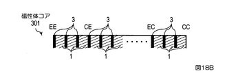
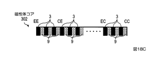
- FIG. 18A to FIG. 18F are schematic views showing the configurations of the magnetic cores 300 to 305 of application examples 19 to 24, respectively.
- the section from the coordinates EE to CC which is the sensing unit existence area set in the second embodiment, to an area including the entire magnetic core.
- the wavelength of the magnetic flux density distribution ⁇ B L H / m (where m is the same) under the condition of S ⁇ 2L H
- the compensation relationship is established as described in FIG. Therefore, in this embodiment, the region from the left end of the core to the right end of the core in the drawing is set as coordinates EE to CC, and the application examples 13 to 18 of the second embodiment are modified to be application examples 19 to 24.
- the magnetic cores 300 to 305 of the current sensor of the present embodiment in addition to the same effects as those of the first and second embodiments, even if the sensing portion existence region is unknown, the condition of S ⁇ 2L H Since the compensation relationship is established, variations in the current sensor between products (operations) can be suppressed.
- Magnetic material> a plurality of types of magnetic bodies are shown as the first magnetic body 1 to the fourth magnetic body 4, but these magnetic bodies are specifically the above-described soft magnetic materials such as iron and silicon steel. , Permalloy, sendust, permendur, soft ferrite (ferrite sheet), amorphous magnetic alloy (amorphous ribbon), nanocrystal magnetic alloy, electromagnetic steel (non-oriented steel sheet, directional steel sheet) and the like.
- a suitable combination in the case of constituting two kinds of magnetic bodies is a magnetic steel plate and a material having good frequency characteristics, a ferrite and a directional magnetic steel plate, an amorphous magnetic alloy and a directional magnetic steel plate, an amorphous magnetic alloy and a ferrite.
- Non-magnetic material Although shown as the nonmagnetic material 9 in Examples 1 to 3, specifically, the nonmagnetic material means a diamagnetic material or a paramagnetic material.
- FIG. 19 is a diagram schematically showing the change in the magnetic flux total number of cases in which the sensing unit stacking direction length L H is not an integer multiple of the wavelength lambda B.
- FIG. 19 shows an example in which two types of magnetic bodies (first magnetic body 1 and third magnetic body 3) are alternately stacked to form a periodic distribution.
- the first thickness of the magnetic substance 1 and L 1, the third thickness of the magnetic body 3 and L 3.
- L 1 > L 3 it is assumed that L 1 > L 3 .
- the aforementioned wavelength ⁇ B L 1 + L 3 .
- the first magnetic permeability of the magnetic substance 1 and mu 1, the third magnetic permeability of the magnetic body 3 and mu 3.
- ⁇ 1 > ⁇ 3 it is assumed that ⁇ 1 > ⁇ 3 .
- ⁇ A ⁇ L ⁇ L 3 >
- ⁇ L is included in the coordinate section where one layer of the first magnetic body 1 exists
- ⁇ L is included in the coordinate section where one layer of the third magnetic body 3 exists.
- the change ⁇ of the total number of magnetic fluxes of the Hall IC sensing unit 11 becomes the largest.
- ⁇ L is included in the coordinate section where one layer of the first magnetic body 1 exists
- ⁇ L is one layer of the third magnetic body 3.
- the change ⁇ in the total number of magnetic fluxes of the Hall IC sensing unit 11 becomes the largest between the case where the Hall IC sensing unit 11 is included in the coordinate section.
- ⁇ C L 3 ⁇ L ⁇ L 1 >
- ⁇ L is included in a coordinate section where one layer of the first magnetic body 1 exists
- ⁇ L is a coordinate section (length L 3) where one layer of the third magnetic body 3 exists.
- the change ⁇ in the total number of magnetic fluxes of the Hall IC sensing unit 11 is the largest.
- ⁇ L is included in the coordinate section where one layer of the first magnetic body 1 exists
- ⁇ L is one layer of the third magnetic body 3.
- the change ⁇ in the total number of magnetic fluxes of the Hall IC sensing unit 11 is the largest between the case where all the coordinate sections (length L 3 ) are included.
- ⁇ E L 1 ⁇ L>
- ⁇ L includes the entire coordinate section (length L 1 ) in which one layer of the first magnetic body 1 exists
- ⁇ L includes the coordinate section in which one layer of the third magnetic body 3 exists (length L 1 ).
- the change ⁇ in the total number of magnetic fluxes of the Hall IC sensing unit 11 is the largest between the case where all the lengths L 3 ) are included.
- L H is precisely not an integral multiple of the wavelength lambda B, even if the excess length ⁇ L occurs, .DELTA..PHI is sufficiently small, the sensitivity deviation of the Hall element by .DELTA..PHI, product As long as it falls within the measurement error range guaranteed by the For example, the total error of an on-vehicle high-precision sensor for an electric vehicle is about 1%. Therefore, if the allowable value of the error caused by the position variation of the Hall element is considered to be about 1/10 of the total error, the ratio of ⁇ to the total number of magnetic fluxes ⁇ may be about 0.1%.
- the allowable value of the error caused by the position variation of the Hall element is considered to be about 1/10 of the total error
- the ratio of ⁇ to the total number of magnetic fluxes ⁇ may be about 0.1%.
- the material is selected so as to satisfy (the setting of ⁇ 1 and ⁇ 3 ), and the layer thicknesses L 1 and L 3 of each material may be determined. From equation (1), The more the L 3 ⁇ L 1, the .DELTA..PHI / [Phi enough mu 1 and mu 3 is if the approximation becomes It can be seen small.
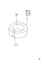
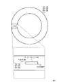
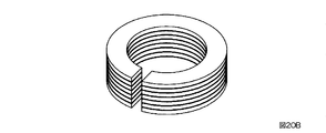
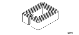
- FIG. 20 is a perspective view showing the shape of the magnetic core provided in the current sensor of the present invention and variations in the stacking direction.
- 20A is an example of a magnetic core laminated in a ring shape and concentric ring
- FIG. 20B is an example of a magnetic core laminated in a ring shape and current conduction direction
- FIG. 20C is a concentric ring having a substantially square C shape. Examples of laminated magnetic cores are shown respectively.
- FIG. 20A is an example of a magnetic core laminated in a ring shape and concentric ring
- FIG. 20B is an example of a magnetic core laminated in a ring shape and current con
- the magnetic core 100 (101 to 108, 200 to 208, 300 to 305) according to the embodiment has been described as having a shape obtained by rounding a plate, but the present invention is not limited to this.
- the shape may be a substantially square C-shape.
- the stacking direction may be any direction other than the circumferential direction. Therefore, as shown in FIG. 20B, the magnetic core may be formed by laminating in the current conduction direction.
- FIG. 20A a flat plate made of a plurality of materials is laminated to form a laminated plate, the laminated plate is formed into a pipe, and then a part of the circumference of the pipe is cut to form a gap. Can be manufactured. This manufacturing process is easy and is one of the preferable manufacturing processes because the gap end surface formed by cutting becomes uniform.
- the magnetic core in FIG. 20A can be manufactured by rounding a laminated plate formed by laminating flat plates made of a plurality of materials into a C shape.
- the magnetic core of FIG. 20C can be manufactured by the same manufacturing method.
- the magnetic core of FIG. 20B In the case of the magnetic core of FIG. 20B, a flat plate made of a plurality of materials is laminated to form a laminated plate, and after punching the laminated plate into a ring shape, a part of the circumference is cut to form a gap. Can be manufactured.
- the magnetic core of FIG. 20B may be formed by alternately laminating a plurality of different ring-shaped sheet materials and then cutting a part of the circumference to form a gap.
Landscapes
- Physics & Mathematics (AREA)
- General Physics & Mathematics (AREA)
- Condensed Matter Physics & Semiconductors (AREA)
- Measuring Instrument Details And Bridges, And Automatic Balancing Devices (AREA)
Abstract
Le but de la présente invention est de fournir un capteur de courant qui, même lors de l'utilisation d'un noyau magnétique formé par une superposition en couches de multiples matériaux magnétiques, est apte à réduire la fluctuation de sensibilité provoquée par une variation de position d'un élément à effet Hall. L'invention est constituée : d'un noyau magnétique, qui comprend un entrefer dans une partie de la périphérie de celui-ci, et qui est formé selon une forme annulaire ; et d'un élément de conversion magnétoélectrique qui est placé dans l'entrefer et détecte un flux magnétique qui varie selon un courant pour une mesure qui passe à travers une partie creuse du noyau magnétique. Le noyau magnétique est caractérisé : en étant formé par une superposition en couches de multiples matériaux magnétiques dans une direction autre que la direction de périphérie ; et en étant formé de telle sorte que des densités de flux magnétique à deux points sont approximativement égales, lesdits points existant dans une zone (mentionnée ci-dessous comme étant 'la zone d'existence de partie de détection') prédéfinie en tant que zone dans laquelle une partie de détection de l'élément de conversion magnétoélectrique est apte à exister, lesdits points étant séparés par une distance dans la direction de superposition en couches qui est la longueur dans la direction de superposition en couches de la partie de détection.
Priority Applications (2)
| Application Number | Priority Date | Filing Date | Title |
|---|---|---|---|
| US14/387,423 US9488679B2 (en) | 2012-05-25 | 2013-03-29 | Current sensor having a laminated magnetic core |
| EP13793450.1A EP2824462B1 (fr) | 2012-05-25 | 2013-03-29 | Capteur de courant |
Applications Claiming Priority (2)
| Application Number | Priority Date | Filing Date | Title |
|---|---|---|---|
| JP2012120132A JP5547234B2 (ja) | 2012-05-25 | 2012-05-25 | 電流センサ |
| JP2012-120132 | 2012-05-25 |
Publications (1)
| Publication Number | Publication Date |
|---|---|
| WO2013175865A1 true WO2013175865A1 (fr) | 2013-11-28 |
Family
ID=49623569
Family Applications (1)
| Application Number | Title | Priority Date | Filing Date |
|---|---|---|---|
| PCT/JP2013/059609 WO2013175865A1 (fr) | 2012-05-25 | 2013-03-29 | Capteur de courant |
Country Status (4)
| Country | Link |
|---|---|
| US (1) | US9488679B2 (fr) |
| EP (1) | EP2824462B1 (fr) |
| JP (1) | JP5547234B2 (fr) |
| WO (1) | WO2013175865A1 (fr) |
Cited By (4)
| Publication number | Priority date | Publication date | Assignee | Title |
|---|---|---|---|---|
| US20150285841A1 (en) * | 2014-04-04 | 2015-10-08 | Cooper Technologies Company | Magnetic sensor with thin-walled magnetic core and methods of manufacture |
| WO2016080135A1 (fr) * | 2014-11-19 | 2016-05-26 | 株式会社東海理化電機製作所 | Capteur de courant |
| CN106501594A (zh) * | 2016-12-25 | 2017-03-15 | 杭州亿为科技有限公司 | 交流电机控制器用电流数字传感器 |
| US20240118319A1 (en) * | 2022-09-21 | 2024-04-11 | Basis NZ Limited | Current detection device and related devices, systems and methods thereof |
Families Citing this family (4)
| Publication number | Priority date | Publication date | Assignee | Title |
|---|---|---|---|---|
| US20170175512A1 (en) * | 2015-12-17 | 2017-06-22 | Schlumberger Technology Corporation | High amplitude magnetic core |
| JP2018004269A (ja) * | 2016-06-27 | 2018-01-11 | アイシン精機株式会社 | 電流センサ |
| JP6544338B2 (ja) * | 2016-11-01 | 2019-07-17 | トヨタ自動車株式会社 | 電流センサ |
| US20220065902A1 (en) * | 2019-02-18 | 2022-03-03 | Panasonic Intellectual Property Management Co., Ltd. | Three-phase current detection device |
Citations (3)
| Publication number | Priority date | Publication date | Assignee | Title |
|---|---|---|---|---|
| JPH05275255A (ja) * | 1992-03-27 | 1993-10-22 | Nippon Steel Corp | 磁気特性の優れたトランスの製造方法 |
| JPH0618977U (ja) * | 1992-08-18 | 1994-03-11 | 三菱電機株式会社 | 電流検出器 |
| JP2008224488A (ja) | 2007-03-14 | 2008-09-25 | Tamura Seisakusho Co Ltd | 電流検出器 |
Family Cites Families (6)
| Publication number | Priority date | Publication date | Assignee | Title |
|---|---|---|---|---|
| FR970066A (fr) * | 1947-08-16 | 1950-12-29 | ||
| FR2764707B1 (fr) * | 1997-06-12 | 1999-07-30 | Schlumberger Ind Sa | Transformateur de mesure |
| US6348800B1 (en) * | 1999-09-28 | 2002-02-19 | Rockwell Automation Technologies, Inc. | Multi-phase ground fault current sensor system |
| JP4479758B2 (ja) * | 2007-07-05 | 2010-06-09 | 株式会社デンソー | 電流センサ用コア |
| JP4424412B2 (ja) * | 2007-11-21 | 2010-03-03 | 株式会社デンソー | 電流センサ |
| JP2013124875A (ja) | 2011-12-13 | 2013-06-24 | Japan Aviation Electronics Industry Ltd | 電流センサ |
-
2012
- 2012-05-25 JP JP2012120132A patent/JP5547234B2/ja not_active Expired - Fee Related
-
2013
- 2013-03-29 EP EP13793450.1A patent/EP2824462B1/fr not_active Not-in-force
- 2013-03-29 WO PCT/JP2013/059609 patent/WO2013175865A1/fr active Application Filing
- 2013-03-29 US US14/387,423 patent/US9488679B2/en active Active
Patent Citations (3)
| Publication number | Priority date | Publication date | Assignee | Title |
|---|---|---|---|---|
| JPH05275255A (ja) * | 1992-03-27 | 1993-10-22 | Nippon Steel Corp | 磁気特性の優れたトランスの製造方法 |
| JPH0618977U (ja) * | 1992-08-18 | 1994-03-11 | 三菱電機株式会社 | 電流検出器 |
| JP2008224488A (ja) | 2007-03-14 | 2008-09-25 | Tamura Seisakusho Co Ltd | 電流検出器 |
Non-Patent Citations (1)
| Title |
|---|
| See also references of EP2824462A4 |
Cited By (6)
| Publication number | Priority date | Publication date | Assignee | Title |
|---|---|---|---|---|
| US20150285841A1 (en) * | 2014-04-04 | 2015-10-08 | Cooper Technologies Company | Magnetic sensor with thin-walled magnetic core and methods of manufacture |
| US10345344B2 (en) * | 2014-04-04 | 2019-07-09 | Eaton Intelligent Power Limited | Magnetic sensor with thin-walled magnetic core and methods of manufacture |
| WO2016080135A1 (fr) * | 2014-11-19 | 2016-05-26 | 株式会社東海理化電機製作所 | Capteur de courant |
| CN106501594A (zh) * | 2016-12-25 | 2017-03-15 | 杭州亿为科技有限公司 | 交流电机控制器用电流数字传感器 |
| US20240118319A1 (en) * | 2022-09-21 | 2024-04-11 | Basis NZ Limited | Current detection device and related devices, systems and methods thereof |
| US12032004B2 (en) * | 2022-09-21 | 2024-07-09 | Basis NZ Limited | Current detection device and related devices, systems and methods thereof |
Also Published As
| Publication number | Publication date |
|---|---|
| EP2824462A4 (fr) | 2015-11-18 |
| JP5547234B2 (ja) | 2014-07-09 |
| EP2824462B1 (fr) | 2016-08-17 |
| US9488679B2 (en) | 2016-11-08 |
| JP2013246056A (ja) | 2013-12-09 |
| EP2824462A1 (fr) | 2015-01-14 |
| US20150084621A1 (en) | 2015-03-26 |
Similar Documents
| Publication | Publication Date | Title |
|---|---|---|
| JP5547234B2 (ja) | 電流センサ | |
| JP5732679B2 (ja) | 電流センサ | |
| US9069016B2 (en) | Current sensor | |
| EP2770333B1 (fr) | Capteur de courant | |
| EP2124067B1 (fr) | Détecteur de courant | |
| JP5619163B2 (ja) | 磁界センサおよび磁界センサ製造方法 | |
| JP6512061B2 (ja) | 電流センサ | |
| WO2013099215A1 (fr) | Capteur de courant | |
| US20160187387A1 (en) | Electrical current transducer with wound magnetic core | |
| JP5957706B2 (ja) | 電流センサ | |
| CN102749491A (zh) | 具有磁芯的电流传感器 | |
| JP2016148620A (ja) | 電流センサ | |
| JP2013246005A (ja) | 電流センサ | |
| JP5516947B2 (ja) | 電流センサ | |
| US8836062B2 (en) | Integrated passive component | |
| JP6251967B2 (ja) | 電流センサ | |
| WO2013161496A1 (fr) | Capteur de courant | |
| US8754643B2 (en) | Coil design for miniaturized fluxgate sensors | |
| JP2014070914A (ja) | 電流センサ | |
| JP4499707B2 (ja) | 電流センサ | |
| WO2011158633A1 (fr) | Capteur de courant et réseau de capteurs de courant | |
| JP2009175019A (ja) | 電流センサ | |
| JP2014202737A (ja) | 電流センサ | |
| JP4459011B2 (ja) | 電流センサ | |
| JP2014098633A (ja) | 電流センサ |
Legal Events
| Date | Code | Title | Description |
|---|---|---|---|
| 121 | Ep: the epo has been informed by wipo that ep was designated in this application |
Ref document number: 13793450 Country of ref document: EP Kind code of ref document: A1 |
|
| WWE | Wipo information: entry into national phase |
Ref document number: 14387423 Country of ref document: US |
|
| REEP | Request for entry into the european phase |
Ref document number: 2013793450 Country of ref document: EP |
|
| WWE | Wipo information: entry into national phase |
Ref document number: 2013793450 Country of ref document: EP |
|
| NENP | Non-entry into the national phase |
Ref country code: DE |