WO2013168688A1 - 有機エレクトロルミネッセンス素子、照明装置及び表示装置 - Google Patents
有機エレクトロルミネッセンス素子、照明装置及び表示装置 Download PDFInfo
- Publication number
- WO2013168688A1 WO2013168688A1 PCT/JP2013/062807 JP2013062807W WO2013168688A1 WO 2013168688 A1 WO2013168688 A1 WO 2013168688A1 JP 2013062807 W JP2013062807 W JP 2013062807W WO 2013168688 A1 WO2013168688 A1 WO 2013168688A1
- Authority
- WO
- WIPO (PCT)
- Prior art keywords
- group
- hydrocarbon ring
- aromatic
- aromatic hydrocarbon
- general formula
- Prior art date
Links
- 0 *[n]1c(c(Ic2c3[n](*)c4ccccc4c3ccc2)ccc2)c2c2ccccc12 Chemical compound *[n]1c(c(Ic2c3[n](*)c4ccccc4c3ccc2)ccc2)c2c2ccccc12 0.000 description 2
Images


Classifications
-
- C—CHEMISTRY; METALLURGY
- C07—ORGANIC CHEMISTRY
- C07D—HETEROCYCLIC COMPOUNDS
- C07D209/00—Heterocyclic compounds containing five-membered rings, condensed with other rings, with one nitrogen atom as the only ring hetero atom
- C07D209/56—Ring systems containing three or more rings
- C07D209/80—[b, c]- or [b, d]-condensed
- C07D209/82—Carbazoles; Hydrogenated carbazoles
- C07D209/86—Carbazoles; Hydrogenated carbazoles with only hydrogen atoms, hydrocarbon or substituted hydrocarbon radicals, directly attached to carbon atoms of the ring system
-
- C—CHEMISTRY; METALLURGY
- C07—ORGANIC CHEMISTRY
- C07D—HETEROCYCLIC COMPOUNDS
- C07D401/00—Heterocyclic compounds containing two or more hetero rings, having nitrogen atoms as the only ring hetero atoms, at least one ring being a six-membered ring with only one nitrogen atom
- C07D401/14—Heterocyclic compounds containing two or more hetero rings, having nitrogen atoms as the only ring hetero atoms, at least one ring being a six-membered ring with only one nitrogen atom containing three or more hetero rings
-
- C—CHEMISTRY; METALLURGY
- C07—ORGANIC CHEMISTRY
- C07D—HETEROCYCLIC COMPOUNDS
- C07D403/00—Heterocyclic compounds containing two or more hetero rings, having nitrogen atoms as the only ring hetero atoms, not provided for by group C07D401/00
- C07D403/14—Heterocyclic compounds containing two or more hetero rings, having nitrogen atoms as the only ring hetero atoms, not provided for by group C07D401/00 containing three or more hetero rings
-
- C—CHEMISTRY; METALLURGY
- C07—ORGANIC CHEMISTRY
- C07D—HETEROCYCLIC COMPOUNDS
- C07D405/00—Heterocyclic compounds containing both one or more hetero rings having oxygen atoms as the only ring hetero atoms, and one or more rings having nitrogen as the only ring hetero atom
- C07D405/14—Heterocyclic compounds containing both one or more hetero rings having oxygen atoms as the only ring hetero atoms, and one or more rings having nitrogen as the only ring hetero atom containing three or more hetero rings
-
- C—CHEMISTRY; METALLURGY
- C07—ORGANIC CHEMISTRY
- C07D—HETEROCYCLIC COMPOUNDS
- C07D409/00—Heterocyclic compounds containing two or more hetero rings, at least one ring having sulfur atoms as the only ring hetero atoms
- C07D409/14—Heterocyclic compounds containing two or more hetero rings, at least one ring having sulfur atoms as the only ring hetero atoms containing three or more hetero rings
-
- C—CHEMISTRY; METALLURGY
- C07—ORGANIC CHEMISTRY
- C07D—HETEROCYCLIC COMPOUNDS
- C07D413/00—Heterocyclic compounds containing two or more hetero rings, at least one ring having nitrogen and oxygen atoms as the only ring hetero atoms
- C07D413/14—Heterocyclic compounds containing two or more hetero rings, at least one ring having nitrogen and oxygen atoms as the only ring hetero atoms containing three or more hetero rings
-
- C—CHEMISTRY; METALLURGY
- C07—ORGANIC CHEMISTRY
- C07F—ACYCLIC, CARBOCYCLIC OR HETEROCYCLIC COMPOUNDS CONTAINING ELEMENTS OTHER THAN CARBON, HYDROGEN, HALOGEN, OXYGEN, NITROGEN, SULFUR, SELENIUM OR TELLURIUM
- C07F15/00—Compounds containing elements of Groups 8, 9, 10 or 18 of the Periodic System
- C07F15/0006—Compounds containing elements of Groups 8, 9, 10 or 18 of the Periodic System compounds of the platinum group
- C07F15/0033—Iridium compounds
-
- C—CHEMISTRY; METALLURGY
- C09—DYES; PAINTS; POLISHES; NATURAL RESINS; ADHESIVES; COMPOSITIONS NOT OTHERWISE PROVIDED FOR; APPLICATIONS OF MATERIALS NOT OTHERWISE PROVIDED FOR
- C09K—MATERIALS FOR MISCELLANEOUS APPLICATIONS, NOT PROVIDED FOR ELSEWHERE
- C09K11/00—Luminescent, e.g. electroluminescent, chemiluminescent materials
- C09K11/06—Luminescent, e.g. electroluminescent, chemiluminescent materials containing organic luminescent materials
-
- H—ELECTRICITY
- H10—SEMICONDUCTOR DEVICES; ELECTRIC SOLID-STATE DEVICES NOT OTHERWISE PROVIDED FOR
- H10K—ORGANIC ELECTRIC SOLID-STATE DEVICES
- H10K85/00—Organic materials used in the body or electrodes of devices covered by this subclass
- H10K85/30—Coordination compounds
- H10K85/341—Transition metal complexes, e.g. Ru(II)polypyridine complexes
- H10K85/342—Transition metal complexes, e.g. Ru(II)polypyridine complexes comprising iridium
-
- C—CHEMISTRY; METALLURGY
- C09—DYES; PAINTS; POLISHES; NATURAL RESINS; ADHESIVES; COMPOSITIONS NOT OTHERWISE PROVIDED FOR; APPLICATIONS OF MATERIALS NOT OTHERWISE PROVIDED FOR
- C09K—MATERIALS FOR MISCELLANEOUS APPLICATIONS, NOT PROVIDED FOR ELSEWHERE
- C09K2211/00—Chemical nature of organic luminescent or tenebrescent compounds
- C09K2211/10—Non-macromolecular compounds
- C09K2211/1003—Carbocyclic compounds
- C09K2211/1007—Non-condensed systems
-
- C—CHEMISTRY; METALLURGY
- C09—DYES; PAINTS; POLISHES; NATURAL RESINS; ADHESIVES; COMPOSITIONS NOT OTHERWISE PROVIDED FOR; APPLICATIONS OF MATERIALS NOT OTHERWISE PROVIDED FOR
- C09K—MATERIALS FOR MISCELLANEOUS APPLICATIONS, NOT PROVIDED FOR ELSEWHERE
- C09K2211/00—Chemical nature of organic luminescent or tenebrescent compounds
- C09K2211/10—Non-macromolecular compounds
- C09K2211/1003—Carbocyclic compounds
- C09K2211/1011—Condensed systems
-
- C—CHEMISTRY; METALLURGY
- C09—DYES; PAINTS; POLISHES; NATURAL RESINS; ADHESIVES; COMPOSITIONS NOT OTHERWISE PROVIDED FOR; APPLICATIONS OF MATERIALS NOT OTHERWISE PROVIDED FOR
- C09K—MATERIALS FOR MISCELLANEOUS APPLICATIONS, NOT PROVIDED FOR ELSEWHERE
- C09K2211/00—Chemical nature of organic luminescent or tenebrescent compounds
- C09K2211/10—Non-macromolecular compounds
- C09K2211/1018—Heterocyclic compounds
- C09K2211/1025—Heterocyclic compounds characterised by ligands
- C09K2211/1029—Heterocyclic compounds characterised by ligands containing one nitrogen atom as the heteroatom
- C09K2211/1033—Heterocyclic compounds characterised by ligands containing one nitrogen atom as the heteroatom with oxygen
-
- C—CHEMISTRY; METALLURGY
- C09—DYES; PAINTS; POLISHES; NATURAL RESINS; ADHESIVES; COMPOSITIONS NOT OTHERWISE PROVIDED FOR; APPLICATIONS OF MATERIALS NOT OTHERWISE PROVIDED FOR
- C09K—MATERIALS FOR MISCELLANEOUS APPLICATIONS, NOT PROVIDED FOR ELSEWHERE
- C09K2211/00—Chemical nature of organic luminescent or tenebrescent compounds
- C09K2211/10—Non-macromolecular compounds
- C09K2211/1018—Heterocyclic compounds
- C09K2211/1025—Heterocyclic compounds characterised by ligands
- C09K2211/1029—Heterocyclic compounds characterised by ligands containing one nitrogen atom as the heteroatom
- C09K2211/1037—Heterocyclic compounds characterised by ligands containing one nitrogen atom as the heteroatom with sulfur
-
- C—CHEMISTRY; METALLURGY
- C09—DYES; PAINTS; POLISHES; NATURAL RESINS; ADHESIVES; COMPOSITIONS NOT OTHERWISE PROVIDED FOR; APPLICATIONS OF MATERIALS NOT OTHERWISE PROVIDED FOR
- C09K—MATERIALS FOR MISCELLANEOUS APPLICATIONS, NOT PROVIDED FOR ELSEWHERE
- C09K2211/00—Chemical nature of organic luminescent or tenebrescent compounds
- C09K2211/10—Non-macromolecular compounds
- C09K2211/1018—Heterocyclic compounds
- C09K2211/1025—Heterocyclic compounds characterised by ligands
- C09K2211/1044—Heterocyclic compounds characterised by ligands containing two nitrogen atoms as heteroatoms
-
- C—CHEMISTRY; METALLURGY
- C09—DYES; PAINTS; POLISHES; NATURAL RESINS; ADHESIVES; COMPOSITIONS NOT OTHERWISE PROVIDED FOR; APPLICATIONS OF MATERIALS NOT OTHERWISE PROVIDED FOR
- C09K—MATERIALS FOR MISCELLANEOUS APPLICATIONS, NOT PROVIDED FOR ELSEWHERE
- C09K2211/00—Chemical nature of organic luminescent or tenebrescent compounds
- C09K2211/10—Non-macromolecular compounds
- C09K2211/1018—Heterocyclic compounds
- C09K2211/1025—Heterocyclic compounds characterised by ligands
- C09K2211/1088—Heterocyclic compounds characterised by ligands containing oxygen as the only heteroatom
-
- C—CHEMISTRY; METALLURGY
- C09—DYES; PAINTS; POLISHES; NATURAL RESINS; ADHESIVES; COMPOSITIONS NOT OTHERWISE PROVIDED FOR; APPLICATIONS OF MATERIALS NOT OTHERWISE PROVIDED FOR
- C09K—MATERIALS FOR MISCELLANEOUS APPLICATIONS, NOT PROVIDED FOR ELSEWHERE
- C09K2211/00—Chemical nature of organic luminescent or tenebrescent compounds
- C09K2211/10—Non-macromolecular compounds
- C09K2211/1018—Heterocyclic compounds
- C09K2211/1025—Heterocyclic compounds characterised by ligands
- C09K2211/1092—Heterocyclic compounds characterised by ligands containing sulfur as the only heteroatom
-
- C—CHEMISTRY; METALLURGY
- C09—DYES; PAINTS; POLISHES; NATURAL RESINS; ADHESIVES; COMPOSITIONS NOT OTHERWISE PROVIDED FOR; APPLICATIONS OF MATERIALS NOT OTHERWISE PROVIDED FOR
- C09K—MATERIALS FOR MISCELLANEOUS APPLICATIONS, NOT PROVIDED FOR ELSEWHERE
- C09K2211/00—Chemical nature of organic luminescent or tenebrescent compounds
- C09K2211/10—Non-macromolecular compounds
- C09K2211/1018—Heterocyclic compounds
- C09K2211/1025—Heterocyclic compounds characterised by ligands
- C09K2211/1096—Heterocyclic compounds characterised by ligands containing other heteroatoms
-
- C—CHEMISTRY; METALLURGY
- C09—DYES; PAINTS; POLISHES; NATURAL RESINS; ADHESIVES; COMPOSITIONS NOT OTHERWISE PROVIDED FOR; APPLICATIONS OF MATERIALS NOT OTHERWISE PROVIDED FOR
- C09K—MATERIALS FOR MISCELLANEOUS APPLICATIONS, NOT PROVIDED FOR ELSEWHERE
- C09K2211/00—Chemical nature of organic luminescent or tenebrescent compounds
- C09K2211/18—Metal complexes
- C09K2211/185—Metal complexes of the platinum group, i.e. Os, Ir, Pt, Ru, Rh or Pd
-
- H—ELECTRICITY
- H10—SEMICONDUCTOR DEVICES; ELECTRIC SOLID-STATE DEVICES NOT OTHERWISE PROVIDED FOR
- H10K—ORGANIC ELECTRIC SOLID-STATE DEVICES
- H10K2101/00—Properties of the organic materials covered by group H10K85/00
- H10K2101/10—Triplet emission
-
- H—ELECTRICITY
- H10—SEMICONDUCTOR DEVICES; ELECTRIC SOLID-STATE DEVICES NOT OTHERWISE PROVIDED FOR
- H10K—ORGANIC ELECTRIC SOLID-STATE DEVICES
- H10K50/00—Organic light-emitting devices
- H10K50/10—OLEDs or polymer light-emitting diodes [PLED]
- H10K50/11—OLEDs or polymer light-emitting diodes [PLED] characterised by the electroluminescent [EL] layers
Definitions
- the present invention relates to an organic electroluminescence element, a lighting device, and a display device.
- An organic electroluminescence element (hereinafter also referred to as an organic EL element) has a configuration in which a light-emitting layer containing a light-emitting compound is sandwiched between a cathode and an anode, and a positive electrode injected from the anode by applying an electric field.
- This is a light emitting device that uses the emission of light (fluorescence / phosphorescence) when excitons are generated by recombining electrons injected from holes and cathodes in the light emitting layer to generate excitons. is there.
- An organic EL element is an all-solid-state element composed of an organic material film with a thickness of only a submicron between electrodes, and can emit light at a voltage of several volts to several tens of volts. It is expected to be used for next-generation flat display and lighting.
- organic EL elements that utilize phosphorescence emission can in principle achieve a light emission efficiency that is approximately four times that of organic EL elements that utilize previous fluorescence emission.
- Research and development of device layer configurations and electrodes are performed all over the world. For example, many compounds have been studied focusing on heavy metal complexes such as iridium complexes.
- the phosphorescence emission method is a method having a very high potential.
- an organic EL device using phosphorescence emission is greatly different from an organic EL device using fluorescence emission, and controls the position of the emission center.
- the method particularly how to recombine within the light emitting layer to stabilize the light emission, is an important technical issue for capturing the efficiency and lifetime of the device.
- a multi-layered element having a hole transport layer located on the anode side of the light emitting layer and an electron transport layer located on the cathode side of the light emitting layer in a form adjacent to the light emitting layer is well known.
- a mixed layer using a host compound and a phosphorescent compound as a dopant is often used for the light emitting layer.
- FIrpic is known as a typical blue phosphorescent compound, and a short wave is realized by substituting fluorine for the main ligand phenylpyridine and using picolinic acid as a secondary ligand. Yes.
- These dopants have achieved high-efficiency devices by combining carbazole derivatives and triarylsilanes as host compounds. However, since the light emission lifetime of the devices is greatly deteriorated, improvement of the trade-off has been demanded. .
- Patent Document 2 As a blue phosphorescent compound having a high potential, a metal complex having a specific ligand has been disclosed in Patent Document 2, and a combined material for extracting the potential of this complex is disclosed in Patent Document 3. It is disclosed.
- an object of the present invention is to improve the thermal stability and sublimation property of a dopant compound of an organic electroluminescence device, and to use a host compound and an adjacent layer material matched to the dopant compound, so that the luminous efficiency is high and the lifetime is long.
- Another object of the present invention is to provide an organic electroluminescence element having a low driving voltage, a lighting device and a display device using the element.
- an organic electroluminescence device in which at least one organic layer including at least one light emitting layer is sandwiched between an anode and a cathode, At least one layer of the light emitting layer contains an iridium complex compound represented by the following general formula (1), A compound represented by the following general formula (2) is contained in at least one of the organic layers.
- An organic electroluminescence device is provided.
- ring Am, ring An, ring Bm and ring Bn represent a 5-membered or 6-membered aromatic hydrocarbon ring or aromatic heterocycle.
- R1m, R2m, R1n and R2n each independently represents an alkyl group having 2 or more carbon atoms, an aromatic hydrocarbon ring group, an aromatic heterocyclic group, a non-aromatic hydrocarbon ring group or a non-aromatic heterocyclic group; It may have a substituent.
- Ra, Rb and Rc are each independently a hydrogen atom, halogen atom, cyano group, alkyl group, alkenyl group, alkynyl group, alkoxy group, amino group, silyl group, arylalkyl group, aryl group, heteroaryl group, non-aromatic It represents a hydrocarbon ring group or a non-aromatic heterocyclic group, and may further have a substituent.
- na represents an integer of 1 to 3
- nb represents an integer of 1 to 4
- nc represents 1 or 2.
- m represents 1 or 2
- n represents 1 or 2
- m + n is 3. Note that the structures of the three ligands coordinated to Ir are not all the same.
- R1 and R2 each independently represent a hydrogen atom, an alkyl group, an aromatic hydrocarbon ring group, an aromatic heterocyclic group, a non-aromatic hydrocarbon ring group, or a non-aromatic heterocyclic group, Furthermore, you may have a substituent.
- L represents a simple bond, an alkylene group, an aromatic hydrocarbon ring group, an aromatic heterocyclic group, a non-aromatic hydrocarbon ring group or a non-aromatic heterocyclic group.
- an organic electroluminescence device in which at least one organic layer including at least one light emitting layer is sandwiched between an anode and a cathode, At least one layer of the light emitting layer contains an iridium complex compound represented by the following general formula (3), A compound represented by the following general formula (2) is contained in at least one of the organic layers.
- An organic electroluminescence device is provided.
- ring Am, ring An, ring Bm and ring Bn represent a 5-membered or 6-membered aromatic hydrocarbon ring or aromatic heterocycle.
- Ar represents an aromatic hydrocarbon ring group, an aromatic heterocyclic group, a non-aromatic hydrocarbon ring group or a non-aromatic heterocyclic group.
- R1m, R2m, R1n and R2n each independently represents an alkyl group having 2 or more carbon atoms, an aromatic hydrocarbon ring group, an aromatic heterocyclic group, a non-aromatic hydrocarbon ring group or a non-aromatic heterocyclic group; It may have a substituent.
- Ra, Rb and Rc are each independently a hydrogen atom, halogen atom, cyano group, alkyl group, alkenyl group, alkynyl group, alkoxy group, amino group, silyl group, arylalkyl group, aryl group, heteroaryl group, non-aromatic It represents a hydrocarbon ring group or a non-aromatic heterocyclic group, may further have a substituent, and Ra may form a ring with Ar.
- na represents an integer of 1 to 3
- nb represents an integer of 1 to 4
- nc represents 1 or 2.
- m represents 1 or 2
- n represents 1 or 2
- m + n is 3. Note that the structures of the three ligands coordinated to Ir are not all the same.
- R1 and R2 each independently represent a hydrogen atom, an alkyl group, an aromatic hydrocarbon ring group, an aromatic heterocyclic group, a non-aromatic hydrocarbon ring group, or a non-aromatic heterocyclic group, Furthermore, you may have a substituent.
- L represents a simple bond, an alkylene group, an aromatic hydrocarbon ring group, an aromatic heterocyclic group, a non-aromatic hydrocarbon ring group or a non-aromatic heterocyclic group.
- an organic electroluminescence device in which at least one organic layer including at least one light emitting layer is sandwiched between an anode and a cathode,
- the iridium complex compound represented by the following general formula (4) is contained in at least one layer of the light emitting layer
- a compound represented by the following general formula (2) is contained in at least one of the organic layers.
- R1m, R2m, R1n and R2n are each independently an alkyl group having 2 or more carbon atoms, an aromatic hydrocarbon ring group, an aromatic heterocyclic group, a non-aromatic hydrocarbon ring group or a non-aromatic group. It represents a heterocyclic group and may further have a substituent.
- Ra, Rc and Ra3 are each independently a hydrogen atom, halogen atom, cyano group, alkyl group, alkenyl group, alkynyl group, alkoxy group, amino group, silyl group, arylalkyl group, aryl group, heteroaryl group, non-aromatic It represents a hydrocarbon ring group or a non-aromatic heterocyclic group, and may further have a substituent.
- na and nc represent 1 or 2
- nR3 represents an integer of 1 to 5.
- m represents 1 or 2
- n represents 1 or 2
- m + n is 3. Note that the structures of the three ligands coordinated to Ir are not all the same.
- R1 and R2 each independently represent a hydrogen atom, an alkyl group, an aromatic hydrocarbon ring group, an aromatic heterocyclic group, a non-aromatic hydrocarbon ring group, or a non-aromatic heterocyclic group, Furthermore, you may have a substituent.
- L represents a simple bond, an alkylene group, an aromatic hydrocarbon ring group, an aromatic heterocyclic group, a non-aromatic hydrocarbon ring group or a non-aromatic heterocyclic group.
- an organic electroluminescence device in which at least one organic layer including at least one light emitting layer is sandwiched between an anode and a cathode, At least one layer of the light emitting layer contains an iridium complex compound represented by the following general formula (5), A compound represented by the following general formula (2) is contained in at least one of the organic layers.
- An organic electroluminescence device is provided.
- R1m, R2m, R1n and R2n are each independently an alkyl group having 2 or more carbon atoms, an aromatic hydrocarbon ring group, an aromatic heterocyclic group, a non-aromatic hydrocarbon ring group or a non-aromatic group. It represents a heterocyclic group and may further have a substituent.
- Ra, Rc and Ra3 are each independently a hydrogen atom, halogen atom, cyano group, alkyl group, alkenyl group, alkynyl group, alkoxy group, amino group, silyl group, arylalkyl group, aryl group, heteroaryl group, non-aromatic It represents a hydrocarbon ring group or a non-aromatic heterocyclic group, and may further have a substituent.
- na and nc represent 1 or 2
- nR3 represents an integer of 1 to 4.
- X represents O, S, SiRz1Rz2, NRz1 or CRz1Rz2, and Rz1 and Rz2 each represents an alkyl group, an aromatic hydrocarbon ring group, an aromatic heterocyclic group, a non-aromatic hydrocarbon ring group, or a non-aromatic heterocyclic group.
- m represents 1 or 2
- n represents 1 or 2
- m + n 3.
- R1 and R2 each independently represent a hydrogen atom, an alkyl group, an aromatic hydrocarbon ring group, an aromatic heterocyclic group, a non-aromatic hydrocarbon ring group, or a non-aromatic heterocyclic group, Furthermore, you may have a substituent.
- L represents a simple bond, an alkylene group, an aromatic hydrocarbon ring group, an aromatic heterocyclic group, a non-aromatic hydrocarbon ring group or a non-aromatic heterocyclic group.
- an organic electroluminescence device in which at least one organic layer including at least one light emitting layer is sandwiched between an anode and a cathode, In at least one layer of the light emitting layer, an iridium complex compound represented by the following general formula (6) is contained, A compound represented by the following general formula (2) is contained in at least one of the organic layers.
- An organic electroluminescence device is provided.
- R1m, R2m, R1n and R2n are each independently an alkyl group having 2 or more carbon atoms, an aromatic hydrocarbon ring group, an aromatic heterocyclic group, a non-aromatic hydrocarbon ring group or a non-aromatic group. It represents a heterocyclic group and may further have a substituent.
- Ra, Rc and Ra3 are each independently a hydrogen atom, halogen atom, cyano group, alkyl group, alkenyl group, alkynyl group, alkoxy group, amino group, silyl group, arylalkyl group, aryl group, heteroaryl group, non-aromatic It represents a hydrocarbon ring group or a non-aromatic heterocyclic group, and may further have a substituent.
- na and nc represent 1 or 2
- nR3 represents an integer of 1 to 4.
- X represents O, S, SiRz1Rz2, NRz1 or CRz1Rz2, and Rz1 and Rz2 each represents an alkyl group, an aromatic hydrocarbon ring group, an aromatic heterocyclic group, a non-aromatic hydrocarbon ring group, or a non-aromatic heterocyclic group.
- m represents 1 or 2
- n represents 1 or 2
- m + n 3.
- R1 and R2 each independently represent a hydrogen atom, an alkyl group, an aromatic hydrocarbon ring group, an aromatic heterocyclic group, a non-aromatic hydrocarbon ring group, or a non-aromatic heterocyclic group, Furthermore, you may have a substituent.
- L represents a simple bond, an alkylene group, an aromatic hydrocarbon ring group, an aromatic heterocyclic group, a non-aromatic hydrocarbon ring group or a non-aromatic heterocyclic group.
- an organic electroluminescence device in which at least one organic layer including at least one light emitting layer is sandwiched between an anode and a cathode, At least one layer of the light emitting layer contains an iridium complex compound represented by the following general formula (1), A compound represented by the following general formula (7) is contained in at least one of the organic layers, and an organic electroluminescence device is provided.
- ring Am, ring An, ring Bm and ring Bn represent a 5-membered or 6-membered aromatic hydrocarbon ring or aromatic heterocycle.
- R1m, R2m, R1n and R2n each independently represents an alkyl group having 2 or more carbon atoms, an aromatic hydrocarbon ring group, an aromatic heterocyclic group, a non-aromatic hydrocarbon ring group or a non-aromatic heterocyclic group; It may have a substituent.
- Ra, Rb and Rc are each independently a hydrogen atom, halogen atom, cyano group, alkyl group, alkenyl group, alkynyl group, alkoxy group, amino group, silyl group, arylalkyl group, aryl group, heteroaryl group, non-aromatic It represents a hydrocarbon ring group or a non-aromatic heterocyclic group, and may further have a substituent.
- na represents an integer of 1 to 3
- nb represents an integer of 1 to 4
- nc represents 1 or 2.
- m represents 1 or 2
- n represents 1 or 2
- m + n is 3. Note that the structures of the three ligands coordinated to Ir are not all the same.
- R1 and R2 each independently represent a hydrogen atom, an alkyl group, an aromatic hydrocarbon ring group, an aromatic heterocyclic group, a non-aromatic hydrocarbon ring group, or a non-aromatic heterocyclic group, Furthermore, you may have a substituent.
- L represents a simple bond, an alkylene group, an aromatic hydrocarbon ring group, an aromatic heterocyclic group, a non-aromatic hydrocarbon ring group or a non-aromatic heterocyclic group.
- an organic electroluminescence device in which at least one organic layer including at least one light emitting layer is sandwiched between an anode and a cathode, At least one layer of the light emitting layer contains an iridium complex compound represented by the following general formula (1), A compound represented by the following general formula (8) is contained in at least one of the organic layers, and an organic electroluminescence device is provided.
- ring Am, ring An, ring Bm and ring Bn represent a 5-membered or 6-membered aromatic hydrocarbon ring or aromatic heterocycle.
- R1m, R2m, R1n and R2n each independently represents an alkyl group having 2 or more carbon atoms, an aromatic hydrocarbon ring group, an aromatic heterocyclic group, a non-aromatic hydrocarbon ring group or a non-aromatic heterocyclic group; It may have a substituent.
- Ra, Rb and Rc are each independently a hydrogen atom, halogen atom, cyano group, alkyl group, alkenyl group, alkynyl group, alkoxy group, amino group, silyl group, arylalkyl group, aryl group, heteroaryl group, non-aromatic It represents a hydrocarbon ring group or a non-aromatic heterocyclic group, and may further have a substituent.
- na represents an integer of 1 to 3
- nb represents an integer of 1 to 4
- nc represents 1 or 2.
- m represents 1 or 2
- n represents 1 or 2
- m + n is 3. Note that the structures of the three ligands coordinated to Ir are not all the same.
- R1 and R2 each independently represent a hydrogen atom, an alkyl group, an aromatic hydrocarbon ring group, an aromatic heterocyclic group, a non-aromatic hydrocarbon ring group, or a non-aromatic heterocyclic group, Furthermore, you may have a substituent.
- L represents a simple bond, an alkylene group, an aromatic hydrocarbon ring group, an aromatic heterocyclic group, a non-aromatic hydrocarbon ring group or a non-aromatic heterocyclic group.
- an organic electroluminescence device in which at least one organic layer including at least one light emitting layer is sandwiched between an anode and a cathode, At least one layer of the light emitting layer contains an iridium complex compound represented by the following general formula (1), A compound represented by the following general formula (9) is contained in at least one layer of the organic layer, and an organic electroluminescence device is provided.
- ring Am, ring An, ring Bm and ring Bn represent a 5-membered or 6-membered aromatic hydrocarbon ring or aromatic heterocycle.
- R1m, R2m, R1n and R2n each independently represents an alkyl group having 2 or more carbon atoms, an aromatic hydrocarbon ring group, an aromatic heterocyclic group, a non-aromatic hydrocarbon ring group or a non-aromatic heterocyclic group; It may have a substituent.
- Ra, Rb and Rc are each independently a hydrogen atom, halogen atom, cyano group, alkyl group, alkenyl group, alkynyl group, alkoxy group, amino group, silyl group, arylalkyl group, aryl group, heteroaryl group, non-aromatic It represents a hydrocarbon ring group or a non-aromatic heterocyclic group, and may further have a substituent.
- na represents an integer of 1 to 3
- nb represents an integer of 1 to 4
- nc represents 1 or 2.
- m represents 1 or 2
- n represents 1 or 2
- m + n is 3. Note that the structures of the three ligands coordinated to Ir are not all the same.
- R1 and R2 each independently represent a hydrogen atom, an alkyl group, an aromatic hydrocarbon ring group, an aromatic heterocyclic group, a non-aromatic hydrocarbon ring group, or a non-aromatic heterocyclic group, Furthermore, you may have a substituent.
- L represents a simple bond, an alkylene group, an aromatic hydrocarbon ring group, an aromatic heterocyclic group, a non-aromatic hydrocarbon ring group or a non-aromatic heterocyclic group.
- a lighting device comprising the organic electroluminescence element.
- a display device comprising the organic electroluminescence element is provided.
- the present invention by improving the thermal stability and sublimation property of the dopant compound of the organic electroluminescence device, and using the host compound and the adjacent layer material matched to the dopant compound, the luminous efficiency is high, the lifetime is low, and the low
- An organic electroluminescence element having a driving voltage, and an illumination device and a display device using the element can be provided.
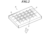
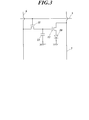
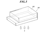
- FIG. 4 is a schematic diagram of a display unit A.
- FIG. It is a schematic diagram of a pixel. It is a schematic diagram of a passive matrix type full-color display device. It is the schematic of an illuminating device. It is a schematic diagram of an illuminating device.
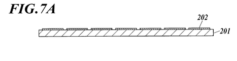
- the schematic block diagram of an organic electroluminescent full color display apparatus is shown.
- the schematic block diagram of an organic electroluminescent full color display apparatus is shown.
- the schematic block diagram of an organic electroluminescent full color display apparatus is shown.
- the schematic block diagram of an organic electroluminescent full color display apparatus is shown.
- the schematic block diagram of an organic electroluminescent full color display apparatus is shown.
- the schematic block diagram of an organic electroluminescent full color display apparatus is shown.
- the schematic block diagram of an organic electroluminescent full color display apparatus is shown.
- the schematic block diagram of an organic electroluminescent full color display apparatus is shown.
- the light emitting layer unit may have a non-light emitting intermediate layer between a plurality of light emitting layers, and may have a multi-photon unit configuration in which the intermediate layer is a charge generation layer.
- the charge generation layer includes ITO (indium tin oxide), IZO (indium zinc oxide), ZnO 2 , TiN, ZrN, HfN, TiO x , VO x , CuI, InN, GaN, CuAlO 2.
- the light emitting layer in the organic EL element of the present invention is preferably a white light emitting layer, and an illumination device using these is preferable.
- the light emitting layer according to the present invention is a layer that emits light by recombination of electrons and holes injected from the electrode or the electron transport layer and the hole transport layer, and the light emitting portion is in the layer of the light emitting layer. May be the interface between the light emitting layer and the adjacent layer.
- the organic EL device according to the present invention has at least one light emitting layer, and may have a plurality of light emitting layers (light emitting layer units).
- the total thickness of the light emitting layer is not particularly limited, but from the viewpoint of improving the uniformity of the film, preventing application of unnecessary high voltage during light emission, and improving the stability of the emission color with respect to the drive current. It is preferably adjusted in the range of 2 nm to 5 ⁇ m, more preferably adjusted in the range of 2 nm to 200 nm, particularly preferably in the range of 5 nm to 100 nm.
- a light-emitting dopant or a host compound which will be described later, is used. And the like can be formed by a method, an inkjet method, a printing method, a spray coating method, a curtain coating method, an LB method (Langmuir Brodgett method, etc.).
- the light emitting layer of the organic EL device of the present invention contains a light emitting dopant (phosphorescent dopant (also referred to as phosphorescent dopant, phosphorescent dopant group) or fluorescent dopant) compound and a light emitting host compound. Is preferred.
- a light emitting dopant phosphorescent dopant (also referred to as phosphorescent dopant, phosphorescent dopant group) or fluorescent dopant) compound and a light emitting host compound. Is preferred.
- Luminescent dopant compound The luminescent dopant compound (a luminescent dopant, a dopant compound, and also only a dopant) is demonstrated.
- a fluorescent dopant also referred to as a fluorescent compound
- a phosphorescent dopant also referred to as a phosphorescent emitter, a phosphorescent compound, a phosphorescent compound, or the like
- a fluorescent dopant also referred to as a fluorescent compound
- a phosphorescent dopant also referred to as a phosphorescent emitter, a phosphorescent compound, a phosphorescent compound, or the like
- the phosphorescent dopant according to the present invention is a compound in which light emission from an excited triplet is observed, specifically, a compound that emits phosphorescence at room temperature (25 ° C.), and has a phosphorescence quantum yield of 25. Although it is defined as a compound of 0.01 or more at ° C., a preferable phosphorescence quantum yield is 0.1 or more.
- the phosphorescent quantum yield can be measured by the method described in Spectroscopic II, page 398 (1992 edition, Maruzen) of the Fourth Edition Experimental Chemistry Course 7. Although the phosphorescence quantum yield in a solution can be measured using various solvents, the phosphorescence dopant according to the present invention achieves the phosphorescence quantum yield (0.01 or more) in any solvent. That's fine.
- the phosphorescent dopant There are two types of light emission of the phosphorescent dopant in principle. One is the recombination of carriers on the host compound to which carriers are transported to generate an excited state of the luminescent host compound, and this energy is used as the phosphorescent dopant. It is an energy transfer type in which light emission from a phosphorescent dopant is obtained by moving to. The other is a carrier trap type in which a phosphorescent dopant serves as a carrier trap, carrier recombination occurs on the phosphorescent dopant, and light emission from the phosphorescent dopant compound is obtained. In any case, it is a condition that the excited state energy of the phosphorescent dopant is lower than the excited state energy of the host compound.
- the present inventors have added an iridium complex compound represented by the following general formula (1) as a dopant compound to the light emitting layer of the organic EL device. It has been clarified that the thermal stability and sublimation property of the organic EL element can be improved by adding as. That is, any one of a plurality of ligands coordinated to an iridium atom is made different from each other, and R1m, R2m, R1n, and R2n in the general formula (1) are substituents having 2 or more carbon atoms.
- the interaction between the iridium complex compounds was relaxed to improve the sublimation property, and further the thermal stability of the iridium complex compounds was improved.
- the said iridium complex compound was formed into a film by vapor deposition and an organic layer was formed, continuous repetition vapor deposition became possible.
- the dopant / dopant interaction was reduced by improving the sublimation property of the dopant compound, it was necessary to design a host compound and an adjacent layer material in accordance with the dopant compound.
- the uniform dispersibility of the dopant compound is improved, and the device The drive voltage could be reduced. Further, by using such a host compound / adjacent layer material, the lifetime of the device could be improved by expanding the light emitting region by improving the carrier balance.
- the host compound / adjacent layer material according to the present invention will be described later.
- Iridium complex compound represented by general formula (1) The iridium complex compound represented by general formula (1) contained in the light emitting layer of the organic EL device of the present invention will be described.
- the iridium complex compound is represented by the following general formula (1).
- ring An, ring Am, ring Bn, and ring Bm represent a 5-membered or 6-membered aromatic hydrocarbon ring or aromatic heterocycle.
- examples of the 5-membered or 6-membered aromatic hydrocarbon ring represented by the ring An, the ring Am, the ring Bn, and the ring Bm include a benzene ring.
- examples of the 5-membered or 6-membered aromatic heterocycle represented by ring An, ring Am, ring Bn and ring Bm include a furan ring, a thiophene ring, an oxazole ring, a pyrrole ring, and a pyridine.
- the rings Bn and Bm are preferably benzene rings, and the rings An and Am are also preferably benzene rings.
- R1m and R2m are each independently an alkyl group having 2 or more carbon atoms, an aromatic hydrocarbon ring group, an aromatic heterocyclic group, a non-aromatic hydrocarbon ring group, or a non-aromatic heterocyclic ring. Represents a group, and may further have a substituent.
- examples of the alkyl group having 2 or more carbon atoms represented by R1m and R2m include an ethyl group, a trifluoromethyl group, an isopropyl group, an n-butyl group, a t-butyl group, and an n-hexyl group. Group, 2-methylhexyl group, pentyl group, adamantyl group, n-decyl group, n-dodecyl group and the like.
- examples of the aromatic hydrocarbon ring group represented by R1m and R2m include a benzene ring, biphenyl ring, naphthalene ring, azulene ring, anthracene ring, phenanthrene ring, pyrene ring, chrysene ring, naphthacene.
- examples of the aromatic heterocyclic group represented by R1m and R2m include a silole ring, a furan ring, a thiophene ring, an oxazole ring, a pyrrole ring, a pyridine ring, a pyridazine ring, a pyrimidine ring, and a pyrazine ring.
- examples of the non-aromatic hydrocarbon ring group represented by R1m and R2m include a cycloalkane (eg, cyclopentane ring, cyclohexane ring, etc.), a cycloalkoxy group (eg, cyclopentyloxy group, Cyclohexyloxy groups, etc.), cycloalkylthio groups (eg, cyclopentylthio groups, cyclohexylthio groups, etc.), cyclohexylaminosulfonyl groups, tetrahydronaphthalene rings, 9,10-dihydroanthracene rings, biphenylene rings, etc. Is mentioned.
- a cycloalkane eg, cyclopentane ring, cyclohexane ring, etc.
- a cycloalkoxy group eg, cyclopentyloxy group, Cyclohexyloxy groups, etc.
- examples of the non-aromatic heterocyclic group represented by R1m and R2m include an epoxy ring, an aziridine ring, a thiirane ring, an oxetane ring, an azetidine ring, a thietane ring, a tetrahydrofuran ring, a dioxolane ring, and a pyrrolidine.
- examples of the substituent that the group represented by R1m and R2m may further include a halogen atom, a cyano group, an alkyl group, an alkenyl group, an alkynyl group, an alkoxy group, and an amino group.
- R1m and R2m are preferably both an alkyl group or a cycloalkyl group having 2 or more carbon atoms, and at least one of R1m and R2m is a branched alkyl group having 3 or more carbon atoms. It is also preferable that there is. More preferably, both R1m and R2m are branched alkyl groups having 3 or more carbon atoms.
- R1n and R2n have the same meanings as R1m and R2m in the general formula (1).
- Ra, Rb and Rc are each independently a hydrogen atom, halogen atom, cyano group, alkyl group, alkenyl group, alkynyl group, alkoxy group, amino group, silyl group, arylalkyl group, aryl Represents a group, a heteroaryl group, a non-aromatic hydrocarbon ring group or a non-aromatic heterocyclic group, and may further have a substituent.
- the aryl group and heteroaryl group represented by Ra, Rb and Rc include the aromatic hydrocarbon ring group and aromatic heterocycle represented by R1m and R2m in the above general formula (1). The same thing as a cyclic group is mentioned.
- examples of the substituent that the group represented by Ra, Rb and Rc may further include a halogen atom, a cyano group, an alkyl group, an alkenyl group, an alkynyl group, an alkoxy group, Examples thereof include an amino group, a silyl group, an arylalkyl group, an aryl group, a heteroaryl group, a non-aromatic hydrocarbon ring group, and a non-aromatic heterocyclic group.
- na represents an integer of 1 to 3
- nb represents an integer of 1 to 4
- nc represents 1 or 2.
- m represents 1 or 2
- n represents 1 or 2
- m + n is 3.
- Iridium complex compound represented by general formula (3) The iridium complex compound represented by general formula (1) is preferably represented by the following general formula (3).
- ring An, ring Am, ring Bn, ring Bm, R1m, R2m, R1n, R2n, Ra, Rb, Rc, na, nb, nc, m and n are the same as in general formula (1).
- Ring An, Ring Am, Ring Bn, Ring Bm, R1m, R2m, R1n, R2n, Ra, Rb, Rc, na, nb, nc, m and n are synonymous.
- Ar represents an aromatic hydrocarbon ring group, an aromatic heterocyclic group, a non-aromatic hydrocarbon ring group, or a non-aromatic heterocyclic group.
- the aromatic hydrocarbon ring group, aromatic heterocyclic group, non-aromatic hydrocarbon ring group or non-aromatic heterocyclic group represented by Ar is R1m in the above general formula (1).
- Ar is preferably an aromatic hydrocarbon ring or an aromatic heterocyclic ring, more preferably an aromatic hydrocarbon ring, and still more preferably a benzene ring.
- iridium complex compounds represented by the general formula (1) or (3) according to the present invention can be synthesized by referring to known methods described in International Publication No. 2006/121811, etc.
- R1m, R2m, R1n, R2n, Ra, Rc, nc, m, and n are R1m, R2m, R1n, R2n, Ra, Rc, nc, m, and n in the general formula (1). It is synonymous.
- Ra3 is synonymous with Ra, Rb, and Rc in General formula (1).
- na represents 1 or 2.
- nR3 represents an integer of 1 to 5.
- the iridium complex compound represented by the general formula (5) The iridium complex compound represented by the above general formula (1) or (3) is represented by the following general formula (5). Is preferred.
- R1m, R2m, R1n, R2n, Ra, Rc, nc, m, and n are R1m, R2m, R1n, R2n, Ra, Rc, nc, m, and n in the general formula (1). It is synonymous.
- Ra3 is synonymous with Ra, Rb, and Rc in General formula (1).
- na represents 1 or 2.
- nR3 represents an integer of 1 to 4.
- X represents O, S, SiRz1Rz2, NRz1 or CRz1Rz2, and Rz1 and Rz2 are alkyl groups, aromatic hydrocarbon ring groups, aromatic heterocyclic groups, non-aromatic hydrocarbon ring groups or Represents a non-aromatic heterocyclic group.
- the aromatic hydrocarbon ring group, aromatic heterocyclic group, non-aromatic hydrocarbon ring group or non-aromatic heterocyclic group represented by Rz1 and Rz2 is represented by R1m and R2m in the above general formula (1).
- Rz1 and Rz2 is represented by R1m and R2m in the above general formula (1).
- the iridium complex compound represented by the general formula (6) (1.1.5) The iridium complex compound represented by the general formula (6)
- the iridium complex compound represented by the above general formula (1) or (3) is represented by the following general formula (6). Is preferred.
- R1m, R2m, R1n, R2n, Ra, Rc, nc, m, and n are R1m, R2m, R1n, R2n, Ra, Rc, nc, m, and n in the general formula (1). It is synonymous.
- Ra3 is synonymous with Ra, Rb, and Rc in General formula (1).
- nR3 represents an integer of 1 to 4.
- na represents 1 or 2.
- X is synonymous with X in General formula (5).
- Fluorescent dopant also called fluorescent compound
- fluorescent dopants coumarin dyes, pyran dyes, cyanine dyes, croconium dyes, squalium dyes, oxobenzanthracene dyes, fluorescein dyes, rhodamine dyes, pyrylium dyes, perylene dyes, stilbene dyes , Polythiophene dyes, rare earth complex phosphors, and the like, and compounds having a high fluorescence quantum yield such as laser dyes.
- the luminescent dopant according to the present invention may be used in combination with a plurality of types of compounds, a combination of phosphorescent dopants having different structures, a phosphorescent dopant and A combination of fluorescent dopants may also be used.
- Luminescent host compound also referred to as luminescent host or host compound
- the host compound has a mass ratio of 20% or more in the layer, and the phosphorescence quantum yield of phosphorescence emission is 0 at room temperature (25 ° C.). Defined as less than 1 compound.
- the phosphorescence quantum yield is preferably less than 0.01.
- the mass ratio in the layer is 20% or more among the compounds contained in a light emitting layer.
- the light-emitting host that can be used in the present invention is not particularly limited, and compounds conventionally used in organic EL devices can be used.
- a compound that has a hole transporting ability and an electron transporting ability, prevents the emission of light from being increased in wavelength, and has a high Tg (glass transition temperature) is preferable.
- a conventionally known light-emitting host may be used alone, or a plurality of types may be used in combination.
- the movement of charges can be adjusted, and the organic EL element can be made highly efficient.
- it becomes possible to mix different light emission by using multiple types of the metal complex of this invention used as said phosphorescence dopant, and / or a conventionally well-known compound, and, thereby, arbitrary luminescent colors can be obtained.
- the light emitting host used in the present invention may be a low molecular compound, a high molecular compound having a repeating unit, or a low molecular compound having a polymerizable group such as a vinyl group or an epoxy group (polymerizable light emitting host). Of course, one or more of such compounds may be used.
- the light emitting layer of the organic EL device contains the iridium complex compound represented by the general formula (1) or (3) to (6) as a dopant compound, and the iridium complex compound.
- a host compound that can be preferably combined with the compound include a compound represented by the following general formula (2).
- the compound represented by following General formula (2) is contained as a host compound in the light emitting layer of an organic EL element, it is good also as what is contained in organic layers other than a light emitting layer.
- the compound represented by the general formula (2) is preferably contained in the electron blocking layer as described later.
- R1 and R2 each independently represent a hydrogen atom, an alkyl group, an aromatic hydrocarbon ring group, an aromatic heterocyclic group, a non-aromatic hydrocarbon ring group, or a non-aromatic heterocyclic group. Further, it may have a substituent.
- examples of the alkyl group represented by R1 and R2 are the same as the alkyl group having 2 or more carbon atoms represented by R1m and R2m in the general formula (1). Things.
- the aromatic hydrocarbon ring group, aromatic heterocyclic group, non-aromatic hydrocarbon ring group or non-aromatic heterocyclic group represented by R1 and R2 is the above-described general formula (1
- the same aromatic hydrocarbon ring group, aromatic heterocyclic group, non-aromatic hydrocarbon ring group or non-aromatic heterocyclic group represented by R1m and R2m is the same.
- the group represented by R1 and R2 may have a group represented by R1m and R2m in the general formula (1). The same thing as a substituent is mentioned.
- any one of R1 and R2 is preferably an aromatic hydrocarbon ring group or an aromatic heterocyclic group, and more preferably a phenyl group, dibenzofuran, dibenzothiophene or carbazole.
- L represents a simple bond, an alkylene group, an aromatic hydrocarbon ring group, an aromatic heterocyclic group, a non-aromatic hydrocarbon ring group, or a non-aromatic heterocyclic group.
- examples of the alkylene group represented by L include a methylene group and two alkylene groups derived from an alkyl group having 2 or more carbon atoms represented by R1m and R2m in the general formula (1).
- the aromatic hydrocarbon ring group, the aromatic heterocyclic group, the non-aromatic hydrocarbon ring group or the non-aromatic heterocyclic group represented by L can be represented by the above general formula (1). Examples thereof include a divalent group derived from an aromatic hydrocarbon ring group, an aromatic heterocyclic group, a non-aromatic hydrocarbon ring group, or a non-aromatic heterocyclic group represented by R1m and R2m.
- L is preferably a simple bond, an aromatic hydrocarbon ring group or an aromatic heterocyclic group, and more preferably a phenylene group, dibenzofuran, dibenzothiophene or carbazole.
- R1, R2 and L have the same meanings as R1, R2 and L in the general formula (2).
- R1, R2 and L have the same meanings as R1, R2 and L in the general formula (2).
- R1, R2 and L are synonymous with R1, R2 and L in the general formula (2).
- the electron transport layer is made of a material having a function of transporting electrons, and in a broad sense, an electron injection layer and a hole blocking layer are also included in the electron transport layer.
- the electron transport layer can be provided with a single layer or a plurality of layers.
- the electron transport layer only needs to have a function of transmitting electrons injected from the cathode to the light emitting layer.
- any conventionally known compound may be selected and used in combination. Is possible.
- electron transport materials examples include polycyclic aromatic hydrocarbons such as nitro-substituted fluorene derivatives, diphenylquinone derivatives, thiopyran dioxide derivatives, naphthalene perylene, Ring tetracarboxylic anhydride, carbodiimide, fluorenylidenemethane derivative, anthraquinodimethane and anthrone derivative, oxadiazole derivative, carboline derivative, or at least carbon atoms of the hydrocarbon ring constituting the carboline ring of the carboline derivative Derivatives having a ring structure, one of which is substituted with a nitrogen atom, hexaazatriphenylene derivatives and the like.
- polycyclic aromatic hydrocarbons such as nitro-substituted fluorene derivatives, diphenylquinone derivatives, thiopyran dioxide derivatives, naphthalene perylene, Ring tetracarboxylic anhydride, carbod
- a thiadiazole derivative in which the oxygen atom of the oxadiazole ring is substituted with a sulfur atom, or a quinoxaline derivative having a quinoxaline ring known as an electron-withdrawing group can also be used as an electron transport material. It is also possible to use a polymer material in which these materials are introduced into a polymer chain or these materials are used as a polymer main chain.
- metal complexes of 8-quinolinol derivatives such as tris (8-quinolinol) aluminum (Alq), tris (5,7-dichloro-8-quinolinol) aluminum, tris (5,7-dibromo-8-quinolinol) aluminum Tris (2-methyl-8-quinolinol) aluminum, tris (5-methyl-8-quinolinol) aluminum, bis (8-quinolinol) zinc (Znq), and the like, and the central metals of these metal complexes are In, Mg, Metal complexes replaced with Cu, Ca, Sn, Ga or Pb can also be used as the electron transport material.
- metal-free or metal phthalocyanine, or those having terminal ends substituted with an alkyl group or a sulfonic acid group can also be used as the electron transport material.
- An inorganic semiconductor such as n-type-Si and n-type-SiC can also be used as an electron transport material.
- the electron transport layer is made of an electron transport material such as a vacuum deposition method, a wet method (also referred to as a wet process, such as a spin coating method, a casting method, a die coating method, a blade coating method, a roll coating method, an ink jet method, a printing method, or a spraying method.
- the film is preferably formed by thinning by a coating method, curtain coating method, LB method (Langmuir Brodgett method, etc.).
- the film thickness of the electron transport layer is not particularly limited, but is usually about 5 nm to 5000 nm, preferably 5 nm to 200 nm.
- This electron transport layer may have a single layer structure composed of one or more of the above materials.
- an n-type dopant such as a metal compound such as a metal complex or a metal halide may be doped.
- cathode a material having a low work function (4 eV or less) metal (referred to as an electron injecting metal), an alloy, an electrically conductive compound, and a mixture thereof as an electrode material is used.
- electrode materials include sodium, sodium-potassium alloy, magnesium, lithium, magnesium / copper mixture, magnesium / silver mixture, magnesium / aluminum mixture, magnesium / indium mixture, aluminum / aluminum oxide (Al 2 O 3 ) Mixtures, indium, lithium / aluminum mixtures, rare earth metals and the like.
- a mixture of an electron injecting metal and a second metal which is a stable metal having a larger work function than this for example, a magnesium / silver mixture, Magnesium / aluminum mixtures, magnesium / indium mixtures, aluminum / aluminum oxide (Al 2 O 3 ) mixtures, lithium / aluminum mixtures, aluminum and the like are preferred.
- the cathode can be produced by forming a thin film of these electrode materials by a method such as vapor deposition or sputtering.
- the sheet resistance as the cathode is preferably several hundred ⁇ / ⁇ or less, and the film thickness is usually selected in the range of 10 nm to 5 ⁇ m, preferably 50 nm to 200 nm.
- a transparent or semi-transparent cathode can be produced by producing the above metal on the cathode in a thickness of 1 nm to 20 nm and then producing a conductive transparent material mentioned in the explanation of the anode described later. By applying this, an element in which both the anode and the cathode are transmissive can be manufactured.
- Injection layer electron injection layer (cathode buffer layer), hole injection layer >> The injection layer is provided as necessary, and there are an electron injection layer and a hole injection layer, and as described above, it exists between the anode and the light emitting layer or the hole transport layer and between the cathode and the light emitting layer or the electron transport layer. May be.
- An injection layer is a layer provided between an electrode and an organic layer in order to reduce drive voltage and improve light emission luminance.
- Organic EL element and its forefront of industrialization (issued by NTT Corporation on November 30, 1998) ) ”, Chapter 2,“ Electrode Materials ”(pages 123 to 166), which has a hole injection layer (anode buffer layer) and an electron injection layer (cathode buffer layer).
- anode buffer layer hole injection layer
- copper phthalocyanine is used.
- cathode buffer layer (electron injection layer) The details of the cathode buffer layer (electron injection layer) are described in JP-A-6-325871, JP-A-9-17574, JP-A-10-74586, and the like. Specifically, strontium, aluminum, etc.
- Metal buffer layer typified by, alkali metal compound buffer layer typified by lithium fluoride and potassium fluoride, alkaline earth metal compound buffer layer typified by magnesium fluoride and cesium fluoride, typified by aluminum oxide Examples thereof include an oxide buffer layer.
- the buffer layer (injection layer) is preferably a very thin film, and the film thickness is preferably in the range of 0.1 nm to 5 ⁇ m, although it depends on the material.
- ⁇ Blocking layer hole blocking layer, electron blocking layer>
- the blocking layer is provided as necessary in addition to the basic constituent layer of the organic compound thin film as described above. For example, it is described in JP-A Nos. 11-204258 and 11-204359, and “Organic EL elements and the forefront of industrialization (published by NTT Corporation on November 30, 1998)” on page 237. There is a hole blocking (hole blocking) layer.
- the hole blocking layer has a function of an electron transport layer in a broad sense, and is made of a hole blocking material that has a function of transporting electrons and has a remarkably small ability to transport holes. The probability of recombination of electrons and holes can be improved by blocking.
- the structure of the electron transport layer described above can be used as a hole blocking layer according to the present invention, if necessary.
- the hole blocking layer of the organic EL device of the present invention is preferably provided adjacent to the light emitting layer.
- the hole blocking layer includes a carbazole derivative, a carboline derivative, a diazacarbazole derivative (the diazacarbazole derivative is a nitrogen atom in which any one of carbon atoms constituting the carboline ring is mentioned as the host compound described above. It is preferable to contain (represented by).
- the light emitting layer having the shortest wavelength of light emission is preferably closest to the anode among all the light emitting layers.
- 50% by mass or more of the compound contained in the hole blocking layer provided at the position has an ionization potential of 0.3 eV or more larger than the host compound of the shortest wave emitting layer.
- the ionization potential is defined by the energy required to emit electrons at the HOMO (highest occupied orbital) level of the compound to the vacuum level, and can be determined by, for example, the following method.
- Gaussian 98 Gaussian 98, Revision A.11.4, MJ Frisch, et al, Gaussian, Inc., Pittsburgh PA, 2002.
- a molecular orbital calculation software manufactured by Gaussian, USA.
- eV unit converted value As a value (eV unit converted value) calculated by performing structure optimization using B3LYP / 6-31G *. This calculation value is effective because the correlation between the calculation value obtained by this method and the experimental value is high.
- the ionization potential can also be obtained by a method of directly measuring by photoelectron spectroscopy. For example, a low energy electron spectrometer “Model AC-1” manufactured by Riken Keiki Co., Ltd. or a method known as ultraviolet photoelectron spectroscopy can be suitably used.
- the electron blocking layer has a function of a hole transport layer in a broad sense, and is made of a material that has a function of transporting holes and has an extremely small ability to transport electrons, and transports electrons while transporting holes. By blocking, the recombination probability of electrons and holes can be improved.
- the structure of the hole transport layer described later can be used as an electron blocking layer as necessary.
- the film thickness of the hole blocking layer and the electron transport layer according to the present invention is preferably 3 nm to 100 nm, and more preferably 5 nm to 30 nm.
- the organic EL device of the present invention preferably has an electron blocking layer as an organic layer, and the electron blocking layer includes a compound represented by the above general formula (2) or (7) to (9). Is preferably contained.
- the electron blocking layer is preferably provided between the light emitting layer and the hole transport layer.
- the hole transport layer is made of a hole transport material having a function of transporting holes, and in a broad sense, a hole injection layer and an electron blocking layer are also included in the hole transport layer.
- the hole transport layer can be provided as a single layer or a plurality of layers.
- the hole transport material has any one of hole injection or transport and electron barrier properties, and may be either organic or inorganic.
- triazole derivatives, oxadiazole derivatives, imidazole derivatives, polyarylalkane derivatives, pyrazoline derivatives and pyrazolone derivatives, phenylenediamine derivatives, arylamine derivatives, amino-substituted chalcone derivatives, oxazole derivatives, styrylanthracene derivatives, fluorenone derivatives, hydrazone derivatives examples thereof include stilbene derivatives, silazane derivatives, aniline copolymers, and conductive polymer oligomers, particularly thiophene oligomers.
- azatriphenylene derivatives such as those described in JP-T-2003-519432 and JP-A-2006-135145 can also be used as hole transport materials.
- the above-mentioned materials can be used as the hole transport material, but it is preferable to use a porphyrin compound, an aromatic tertiary amine compound and a styrylamine compound, particularly an aromatic tertiary amine compound.
- aromatic tertiary amine compounds and styrylamine compounds include N, N, N ′, N′-tetraphenyl-4,4′-diaminophenyl; N, N′-diphenyl-N, N′— Bis (3-methylphenyl)-[1,1′-biphenyl] -4,4′-diamine (TPD); 2,2-bis (4-di-p-tolylaminophenyl) propane; 1,1-bis (4-di-p-tolylaminophenyl) cyclohexane; N, N, N ′, N′-tetra-p-tolyl-4,4′-diaminobiphenyl; 1,1-bis (4-di-p-tolyl) Aminophenyl) -4-phenylcyclohexane; bis (4-dimethylamino-2-methylphenyl) phenylmethane; bis (4-di-p-tolylaminoph
- a polymer material in which these materials are introduced into a polymer chain or these materials are used as a polymer main chain can also be used.
- inorganic compounds such as p-type-Si and p-type-SiC can also be used as the hole injection material and the hole transport material.
- JP-A-11-251067 J. Org. Huang et. al.
- a so-called p-type hole transport material described in a book (Applied Physics Letters 80 (2002), p. 139) can also be used.
- these materials are preferably used because a light-emitting element with higher efficiency can be obtained.
- the hole transport layer can be formed by thinning the hole transport material by a known method such as a vacuum deposition method, a spin coating method, a casting method, a printing method including an ink jet method, or an LB method. it can.
- the thickness of the hole transport layer is not particularly limited, but is usually about 5 nm to 5 ⁇ m, preferably 5 nm to 200 nm.
- the hole transport layer may have a single layer structure composed of one or more of the above materials.
- a hole transport layer having a high p property doped with impurities can be used.
- examples thereof include JP-A-4-297076, JP-A-2000-196140, and JP-A-2001-102175. Appl. Phys. 95, 5773 (2004), and the like.
- anode As the anode in the organic EL element, an electrode material made of a metal, an alloy, an electrically conductive compound, or a mixture thereof having a high work function (4 eV or more) is preferably used. Specific examples of such electrode substances include metals such as Au, and conductive transparent materials such as CuI, indium tin oxide (ITO), SnO 2 , and ZnO.
- an amorphous material such as IDIXO (In 2 O 3 —ZnO) capable of forming a transparent conductive film may be used.
- these electrode materials may be formed into a thin film by a method such as vapor deposition or sputtering, and a pattern having a desired shape may be formed by a photolithography method, or when pattern accuracy is not so high (about 100 ⁇ m or more)
- a pattern may be formed through a mask having a desired shape at the time of vapor deposition or sputtering of the electrode material.
- a wet film forming method such as a printing method or a coating method can be used.
- the transmittance be greater than 10%, and the sheet resistance as the anode is preferably several hundred ⁇ / ⁇ or less.
- the film thickness depends on the material, it is usually selected in the range of 10 nm to 1000 nm, preferably 10 nm to 200 nm.
- a support substrate (hereinafter also referred to as a substrate, substrate, substrate, support, etc.) that can be used in the organic EL device of the present invention, there is no particular limitation on the type of glass, plastic, etc., and it is transparent. May be opaque. When extracting light from the support substrate side, the support substrate is preferably transparent. Examples of the transparent support substrate preferably used include glass, quartz, and a transparent resin film. A particularly preferable support substrate is a resin film capable of giving flexibility to the organic EL element.
- polyesters such as polyethylene terephthalate (PET) and polyethylene naphthalate (PEN), polyethylene, polypropylene, cellophane, cellulose diacetate, cellulose triacetate, cellulose acetate butyrate, cellulose acetate propionate (CAP), Cellulose esters such as cellulose acetate phthalate (TAC) and cellulose nitrate or derivatives thereof, polyvinylidene chloride, polyvinyl alcohol, polyethylene vinyl alcohol, syndiotactic polystyrene, polycarbonate, norbornene resin, polymethylpentene, polyether ketone, polyimide , Polyethersulfone (PES), polyphenylene sulfide, polysulfone , Polyetherimide, polyetherketoneimide, polyamide, fluororesin, nylon, polymethylmethacrylate, acrylic or polyarylates, cyclone resins such as Arton (trade name JSR) or Appel (trade name Mits
- an inorganic film, an organic film or a hybrid film of both may be formed on the surface of the resin film.
- the water vapor permeability (25 ⁇ 0.5 ° C.) measured by a method according to JIS K 7129-1992. , Relative humidity (90 ⁇ 2)% RH) is preferably 0.01 g / (m 2 ⁇ 24 h) or less, and further, oxygen measured by a method according to JIS K 7126-1987.
- a high barrier film having a permeability of 10 ⁇ 3 ml / (m 2 ⁇ 24 h ⁇ atm) or less and a water vapor permeability of 10 ⁇ 5 g / (m 2 ⁇ 24 h) or less is preferable.
- the material for forming the barrier film may be any material that has a function of suppressing intrusion of elements that cause deterioration of elements such as moisture and oxygen.
- silicon oxide, silicon dioxide, silicon nitride, or the like can be used.
- the method for forming the barrier film is not particularly limited.
- the vacuum deposition method, sputtering method, reactive sputtering method, molecular beam epitaxy method, cluster ion beam method, ion plating method, plasma polymerization method, atmospheric pressure plasma weight A combination method, a plasma CVD method, a laser CVD method, a thermal CVD method, a coating method, and the like can be used, but an atmospheric pressure plasma polymerization method as described in JP-A-2004-68143 is particularly preferable.
- the opaque support substrate examples include metal plates such as aluminum and stainless steel, films, opaque resin substrates, ceramic substrates, and the like.
- the external extraction efficiency at room temperature of light emission of the organic EL device of the present invention is preferably 1% or more, and more preferably 5% or more.
- the external extraction quantum efficiency (%) the number of photons emitted to the outside of the organic EL element / the number of electrons sent to the organic EL element ⁇ 100.
- a hue improvement filter such as a color filter may be used in combination, or a color conversion filter that converts the emission color from the organic EL element into multiple colors using a phosphor may be used in combination.
- the ⁇ max of light emission of the organic EL element is preferably 480 nm or less.
- a thin film made of a desired electrode material for example, an anode material, is formed on a suitable substrate so as to have a thickness of 1 ⁇ m or less, preferably 10 nm to 200 nm, and an anode is manufactured.
- a thin film containing an organic compound such as a hole injection layer, a hole transport layer, a light emitting layer, a hole blocking layer, an electron transport layer, or a cathode buffer layer, which is an element material, is formed thereon.
- the thin film can be formed by a vacuum deposition method, a wet method (also referred to as a wet process), or the like.
- Wet methods include spin coating, casting, die coating, blade coating, roll coating, ink jet, printing, spray coating, curtain coating, and LB, but precise thin films can be formed.
- a method having high suitability for a roll-to-roll method such as a die coating method, a roll coating method, an ink jet method, and a spray coating method is preferable. Different film formation methods may be applied for each layer.
- liquid medium for dissolving or dispersing the organic EL material according to the present invention examples include ketones such as methyl ethyl ketone and cyclohexanone, fatty acid esters such as ethyl acetate, halogenated hydrocarbons such as dichlorobenzene, toluene, xylene, and mesitylene.
- Aromatic hydrocarbons such as cyclohexylbenzene, aliphatic hydrocarbons such as cyclohexane, decalin, and dodecane, and organic solvents such as DMF and DMSO can be used.
- a dispersion method it can disperse
- a thin film made of a cathode material is formed thereon so as to have a thickness of 1 ⁇ m or less, preferably in the range of 50 to 200 nm, and a desired organic EL device can be obtained by providing a cathode. .
- the cathode, cathode buffer layer, electron transport layer, hole blocking layer, light emitting layer, hole transport layer, hole injection layer, and anode can be formed in the reverse order.
- the organic EL device of the present invention it is preferable to produce from the hole injection layer to the cathode consistently by a single evacuation, but it may be taken out halfway and subjected to different film forming methods. At that time, it is preferable to perform the work in a dry inert gas atmosphere.
- ⁇ Sealing> As a sealing means used for this invention, the method of adhere
- the sealing member may be disposed so as to cover the display area of the organic EL element, and may be a concave plate shape or a flat plate shape. Further, transparency and electrical insulation are not particularly limited.
- Specific examples include a glass plate, a polymer plate / film, and a metal plate / film.
- the glass plate include soda-lime glass, barium / strontium-containing glass, lead glass, aluminosilicate glass, borosilicate glass, barium borosilicate glass, and quartz.
- the polymer plate include those formed from polycarbonate, acrylic, polyethylene terephthalate, polyether sulfide, polysulfone and the like.
- Examples of the metal plate include those made of one or more metals or alloys selected from the group consisting of stainless steel, iron, copper, aluminum, magnesium, nickel, zinc, chromium, titanium, molybdenum, silicon, germanium, and tantalum.
- a polymer film and a metal film can be preferably used because the element can be thinned.
- the polymer film has an oxygen permeability measured by a method according to JIS K 7126-1987 of 1 ⁇ 10 ⁇ 3 ml / (m 2 ⁇ 24 h ⁇ atm) or less, and a method according to JIS K 7129-1992. It is preferable that the water vapor permeability (25 ⁇ 0.5 ° C., relative humidity (90 ⁇ 2)% RH) measured in (1) is 1 ⁇ 10 ⁇ 3 g / (m 2 ⁇ 24 h) or less.
- sealing member For processing the sealing member into a concave shape, sandblasting, chemical etching, or the like is used.
- the adhesive include photocuring and thermosetting adhesives having reactive vinyl groups of acrylic acid oligomers and methacrylic acid oligomers, and moisture curing adhesives such as 2-cyanoacrylates. be able to.
- hot-melt type polyamide, polyester, and polyolefin can be mentioned.
- a cationic curing type ultraviolet curing epoxy resin adhesive can be mentioned.
- an organic EL element may deteriorate by heat processing, what can be adhesively cured from room temperature to 80 ° C. is preferable.
- a desiccant may be dispersed in the adhesive.
- coating of the adhesive agent to a sealing part may use commercially available dispenser, and may print like screen printing.
- the electrode and the organic layer are coated on the outside of the electrode facing the support substrate with the organic layer interposed therebetween, and an inorganic or organic layer is formed in contact with the support substrate to form a sealing film.
- the material for forming the film may be any material that has a function of suppressing intrusion of elements that cause deterioration of elements such as moisture and oxygen.
- silicon oxide, silicon dioxide, silicon nitride, or the like may be used. it can.
- vacuum deposition sputtering, reactive sputtering, molecular beam epitaxy, cluster ion beam method, ion plating method, plasma polymerization method, atmospheric pressure plasma
- a polymerization method a plasma CVD method, a laser CVD method, a thermal CVD method, a coating method, or the like can be used.
- an inert gas such as nitrogen or argon, or an inert liquid such as fluorinated hydrocarbon or silicon oil can be injected in the gas phase and liquid phase.
- an inert gas such as nitrogen or argon, or an inert liquid such as fluorinated hydrocarbon or silicon oil
- a vacuum is also possible.
- a hygroscopic compound can also be enclosed inside.
- hygroscopic compound examples include metal oxides (for example, sodium oxide, potassium oxide, calcium oxide, barium oxide, magnesium oxide, aluminum oxide) and sulfates (for example, sodium sulfate, calcium sulfate, magnesium sulfate, cobalt sulfate).
- metal oxides for example, sodium oxide, potassium oxide, calcium oxide, barium oxide, magnesium oxide, aluminum oxide
- sulfates for example, sodium sulfate, calcium sulfate, magnesium sulfate, cobalt sulfate.
- metal halides eg calcium chloride, magnesium chloride, cesium fluoride, tantalum fluoride, cerium bromide, magnesium bromide, barium iodide, magnesium iodide etc.
- perchloric acids eg perchloric acid Barium, magnesium perchlorate, and the like
- anhydrous salts are preferably used in sulfates, metal halides, and perchloric acids.
- a protective film or a protective plate may be provided on the outer side of the sealing film on the side facing the support substrate with the organic layer interposed therebetween or on the sealing film.
- the mechanical strength is not necessarily high, and thus it is preferable to provide such a protective film and a protective plate.
- the same glass plate, polymer plate / film, metal plate / film, and the like used for the sealing can be used, but the polymer film is light and thin. Is preferably used.
- the organic EL element emits light inside a layer having a refractive index higher than that of air (refractive index is about 1.7 to 2.1) and can extract only about 15% to 20% of the light generated in the light emitting layer. It is generally said. This is because light incident on the interface (interface between the transparent substrate and air) at an angle ⁇ greater than the critical angle causes total reflection and cannot be taken out of the device, or between the transparent electrode or light emitting layer and the transparent substrate. This is because the light undergoes total reflection between the light and the light, and the light is guided through the transparent electrode or the light emitting layer.
- a method of improving the light extraction efficiency for example, a method of forming irregularities on the surface of the transparent substrate and preventing total reflection at the transparent substrate and the air interface (US Pat. No. 4,774,435), A method for improving efficiency by giving light condensing property to a substrate (Japanese Patent Laid-Open No. 63-314795), a method of forming a reflective surface on the side surface of an element (Japanese Patent Laid-Open No. 1-220394), light emission from a substrate A method of forming an antireflection film by introducing a flat layer having an intermediate refractive index between the bodies (Japanese Patent Laid-Open No.
- these methods can be used in combination with the organic EL device of the present invention.
- a method of introducing a flat layer having a lower refractive index than the substrate between the substrate and the light emitter, or a substrate, transparent A method of forming a diffraction grating between any layers of the electrode layer and the light emitting layer (including between the substrate and the outside) can be suitably used.
- the low refractive index layer examples include aerogel, porous silica, magnesium fluoride, and a fluorine-based polymer. Since the refractive index of the transparent substrate is generally about 1.5 to 1.7, the low refractive index layer preferably has a refractive index of about 1.5 or less. Further, it is preferably 1.35 or less.
- the thickness of the low refractive index medium is preferably at least twice the wavelength in the medium. This is because the effect of the low refractive index layer is diminished when the thickness of the low refractive index medium is about the wavelength of light and the electromagnetic wave that has exuded by evanescent enters the substrate.
- the method of introducing a diffraction grating into an interface or any medium that causes total reflection is characterized by a high effect of improving light extraction efficiency.
- This method uses the property that the diffraction grating can change the direction of light to a specific direction different from refraction by so-called Bragg diffraction such as first-order diffraction and second-order diffraction.
- Light that cannot be emitted due to total internal reflection between layers is diffracted by introducing a diffraction grating in any layer or medium (in a transparent substrate or transparent electrode), and the light is removed. I want to take it out.
- the diffraction grating to be introduced has a two-dimensional periodic refractive index. This is because light emitted from the light-emitting layer is randomly generated in all directions, so in a general one-dimensional diffraction grating having a periodic refractive index distribution only in a certain direction, only light traveling in a specific direction is diffracted. Therefore, the light extraction efficiency does not increase so much.
- the refractive index distribution a two-dimensional distribution
- the light traveling in all directions is diffracted, and the light extraction efficiency is increased.
- the position where the diffraction grating is introduced may be in any of the layers or in the medium (in the transparent substrate or the transparent electrode), but is preferably in the vicinity of the organic light emitting layer where light is generated.
- the period of the diffraction grating is preferably about 1/2 to 3 times the wavelength of light in the medium.
- the arrangement of the diffraction grating is preferably two-dimensionally repeated such as a square lattice, a triangular lattice, or a honeycomb lattice.
- the organic EL device of the present invention is processed on the light extraction side of the substrate so as to provide, for example, a microlens array structure, or combined with a so-called condensing sheet, for example, with respect to a specific direction, for example, the device light emitting surface.
- a specific direction for example, the device light emitting surface.
- quadrangular pyramids having a side of 30 ⁇ m and an apex angle of 90 degrees are arranged two-dimensionally on the light extraction side of the substrate.
- One side is preferably 10 ⁇ m to 100 ⁇ m. If it becomes smaller than this, the effect of diffraction will generate
- the condensing sheet for example, a sheet that has been put into practical use for an LED backlight of a liquid crystal display device can be used.
- a sheet for example, a brightness enhancement film (BEF) manufactured by Sumitomo 3M Limited can be used.
- BEF brightness enhancement film
- the shape of the prism sheet for example, the base material may be formed with a triangle stripe having a vertex angle of 90 degrees and a pitch of 50 ⁇ m, or the vertex angle is rounded and the pitch is changed randomly. Other shapes may be used.
- a light diffusion plate / film may be used in combination with the light collecting sheet.
- a diffusion film (light-up) manufactured by Kimoto Co., Ltd. can be used.
- the organic EL element of the present invention can be used as a display device, a display, and various light emission sources.
- lighting devices home lighting, interior lighting
- clock and liquid crystal backlights billboard advertisements, traffic lights, light sources of optical storage media, light sources of electrophotographic copying machines, light sources of optical communication processors, light
- the light source of a sensor etc. are mentioned, It is not limited to this, It can use effectively for the use as a backlight of a liquid crystal display device, and an illumination light source especially.
- patterning may be performed by a metal mask, an ink jet printing method, or the like during film formation, if necessary.
- patterning only the electrode may be patterned, the electrode and the light emitting layer may be patterned, or the entire layer of the element may be patterned.
- a conventionally known method is used. Can do.
- the light emission color of the organic EL device of the present invention and the compound according to the present invention is shown in FIG. 4.16 on page 108 of “New Color Science Handbook” (edited by the Japan Color Society, University of Tokyo Press, 1985). It is determined by the color when the result measured with a total of CS-1000 (manufactured by Konica Minolta Sensing Co., Ltd.) is applied to the CIE chromaticity coordinates.
- the display device of the present invention comprises the organic EL element of the present invention.
- the display device of the present invention may be single color or multicolor, the multicolor display device will be described here.
- a shadow mask is provided only at the time of forming a light emitting layer, and a film can be formed on one surface by vapor deposition, casting, spin coating, ink jet, printing, or the like.
- the method is not limited. However, the vapor deposition method, the ink jet method, the spin coating method, and the printing method are preferable.
- the configuration of the organic EL element included in the display device is selected from the above-described configuration examples of the organic EL element as necessary.
- the manufacturing method of an organic EL element is as having shown in the one aspect
- a DC voltage When a DC voltage is applied to the multicolor display device thus obtained, light emission can be observed by applying a voltage of about 2 V to 40 V with the positive polarity of the anode and the negative polarity of the cathode. Further, even when a voltage is applied with the opposite polarity, no current flows and no light emission occurs. Further, when an AC voltage is applied, light is emitted only when the anode is in the + state and the cathode is in the-state.
- the alternating current waveform to be applied may be arbitrary.
- the multicolor display device can be used as a display device, a display, and various light sources.
- a display device or display full-color display is possible by using three types of organic EL elements of blue, red, and green light emission.
- Display devices and displays include televisions, personal computers, mobile devices, AV devices, teletext displays, information displays in automobiles, and the like. In particular, it may be used as a display device for reproducing still images and moving images, and the driving method when used as a display device for reproducing moving images may be either a simple matrix (passive matrix) method or an active matrix method.
- Light sources include home lighting, interior lighting, clock and liquid crystal backlights, billboard advertisements, traffic lights, light sources for optical storage media, light sources for electrophotographic copying machines, light sources for optical communication processors, light sources for optical sensors, etc.
- the present invention is not limited to these examples.
- FIG. 1 is a schematic view showing an example of a display device composed of organic EL elements. It is a schematic diagram of a display such as a mobile phone that displays image information by light emission of an organic EL element.
- the display 1 includes a display unit A having a plurality of pixels, a control unit B that performs image scanning of the display unit A based on image information, and the like.
- the control unit B is electrically connected to the display unit A, and sends a scanning signal and an image data signal to each of a plurality of pixels based on image information from the outside, and the pixels for each scanning line respond to the image data signal by the scanning signal.
- the image information is sequentially emitted to scan the image and display the image information on the display unit A.
- FIG. 2 is a schematic diagram of the display unit A.
- the display unit A includes a wiring unit including a plurality of scanning lines 5 and data lines 6, a plurality of pixels 3 and the like on a substrate.
- the main members of the display unit A will be described below.
- FIG. 2 shows a case where the light emitted from the pixel 3 is extracted in the direction of the white arrow (downward).
- the scanning line 5 and the plurality of data lines 6 in the wiring portion are each made of a conductive material, and the scanning lines 5 and the data lines 6 are orthogonal to each other in a grid pattern and are connected to the pixels 3 at the orthogonal positions (details are illustrated). Not) When a scanning signal is applied from the scanning line 5, the pixel 3 receives an image data signal from the data line 6 and emits light according to the received image data. Full-color display is possible by appropriately arranging pixels in the red region, the green region, and the blue region on the same substrate.
- FIG. 3 is a schematic diagram of a pixel.
- the pixel includes an organic EL element 10, a switching transistor 11, a driving transistor 12, a capacitor 13, and the like.
- a full color display can be performed by using red, green, and blue light emitting organic EL elements as the organic EL elements 10 in a plurality of pixels, and juxtaposing them on the same substrate.
- an image data signal is applied from the control unit B to the drain of the switching transistor 11 via the data line 6.
- a scanning signal is applied from the control unit B to the gate of the switching transistor 11 via the scanning line 5
- the driving of the switching transistor 11 is turned on, and the image data signal applied to the drain is supplied to the capacitor 13 and the driving transistor 12. Is transmitted to the gate.
- the capacitor 13 is charged according to the potential of the image data signal, and the drive transistor 12 is turned on.
- the drive transistor 12 has a drain connected to the power supply line 7 and a source connected to the electrode of the organic EL element 10.
- the power supply line 7 connects the organic EL element 10 to the potential of the image data signal applied to the gate. Current is supplied.
- the driving of the switching transistor 11 is turned off.
- the driving of the driving transistor 12 is kept on and the next scanning signal is applied. Until then, the light emission of the organic EL element 10 continues.
- the driving transistor 12 is driven according to the potential of the next image data signal synchronized with the scanning signal, and the organic EL element 10 emits light.
- the organic EL element 10 emits light by the switching transistor 11 and the drive transistor 12 that are active elements for the organic EL elements 10 of the plurality of pixels, and the organic EL elements 10 of the plurality of pixels 3 emit light. It is carried out.
- Such a light emitting method is called an active matrix method.
- the light emission of the organic EL element 10 may be light emission of a plurality of gradations by a multi-value image data signal having a plurality of gradation potentials, or by turning on / off a predetermined light emission amount by a binary image data signal. Good.
- the potential of the capacitor 13 may be held continuously until the next scanning signal is applied, or may be discharged immediately before the next scanning signal is applied.
- a passive matrix light emission drive in which the organic EL element emits light according to the data signal only when the scanning signal is scanned.
- FIG. 4 is a schematic diagram of a passive matrix display device.
- a plurality of scanning lines 5 and a plurality of image data lines 6 are provided in a lattice shape so as to face each other with the pixel 3 interposed therebetween.
- the scanning signal of the scanning line 5 is applied by sequential scanning, the pixels 3 connected to the applied scanning line 5 emit light according to the image data signal.
- the pixel 3 has no active element, and the manufacturing cost can be reduced.
- the lighting device of the present invention has the said organic EL element.
- the organic EL element of the present invention may be used as an organic EL element having a resonator structure.
- the purpose of use of the organic EL element having such a resonator structure is as follows.
- the light source of a machine, the light source of an optical communication processing machine, the light source of an optical sensor, etc. are mentioned, However It is not limited to these. Moreover, you may use for the said use by making a laser oscillation.
- the organic EL element of the present invention may be used as a kind of lamp for illumination or exposure light source, a projection device for projecting an image, or a display for directly viewing a still image or a moving image. It may be used as a device (display).
- the driving method when used as a display device for moving image reproduction may be either a simple matrix (passive matrix) method or an active matrix method.
- a full color display device can be produced by using two or more organic EL elements of the present invention having different emission colors.
- the organic EL material of the present invention can be applied to an organic EL element that emits substantially white light as a lighting device.
- a plurality of light emitting colors are simultaneously emitted by a plurality of light emitting materials to obtain white light emission by color mixing.
- the combination of a plurality of emission colors may include three emission maximum wavelengths of the three primary colors of red, green and blue, or two using the complementary colors such as blue and yellow, blue green and orange.
- the thing containing the light emission maximum wavelength may be used.
- a combination of light emitting materials for obtaining a plurality of emission colors is a combination of a plurality of phosphorescent or fluorescent materials, a light emitting material that emits fluorescence or phosphorescence, and light from the light emitting material as excitation light. Any of those combined with a dye material that emits light may be used, but in the white organic EL device according to the present invention, only a combination of a plurality of light-emitting dopants may be mixed.
- an electrode film can be formed by a vapor deposition method, a cast method, a spin coating method, an ink jet method, a printing method, etc., and productivity is also improved. According to this method, unlike the white organic EL device in which light emitting elements of a plurality of colors are arranged in parallel in an array, the elements themselves are luminescent white.
- a luminescent material used for a light emitting layer For example, if it is a backlight in a liquid crystal display element, the metal complex which concerns on this invention so that it may suit the wavelength range corresponding to CF (color filter) characteristic, Any one of known light emitting materials may be selected and combined to be whitened.
- CF color filter
- One aspect of the lighting device of the present invention that includes the organic EL element of the present invention will be described.
- the non-light-emitting surface of the organic EL device of the present invention is covered with a glass case, a glass substrate having a thickness of 300 ⁇ m is used as a sealing substrate, and an epoxy-based photocurable adhesive (LUX TRACK manufactured by Toagosei Co., Ltd.) is used as a sealing material around.
- LC0629B is applied, and this is overlaid on the cathode and brought into close contact with the transparent support substrate, irradiated with UV light from the glass substrate side, cured and sealed, and as shown in FIG. 5 and FIG. Can be formed.
- FIG. 5 shows a schematic diagram of a lighting device, and the organic EL element 101 of the present invention is covered with a glass cover 102 (in addition, the sealing operation with the glass cover is to bring the organic EL element 101 into contact with the atmosphere. And a glove box under a nitrogen atmosphere (in an atmosphere of high-purity nitrogen gas having a purity of 99.999% or more).
- FIG. 6 shows a cross-sectional view of the lighting device.
- 105 denotes a cathode
- 106 denotes an organic EL layer
- 107 denotes a glass substrate with a transparent electrode.
- the glass cover 102 is filled with nitrogen gas 108 and a water catching agent 109 is provided.
- the supporting substrate was ultrasonically cleaned with isopropyl alcohol, dried with dry nitrogen gas, and UV ozone cleaning was performed for 5 minutes.
- PEDOT / PSS polystyrene sulfonate
- This transparent support substrate is fixed to a substrate holder of a commercially available vacuum deposition apparatus, while 200 mg of ⁇ -NPD is added as a hole transport material to a resistance heating boat made of molybdenum, and as a host compound in another resistance heating boat made of molybdenum.
- 200 mg of ET-8 as an electron transport material was put into another molybdenum resistance heating boat, and 100 mg of Comparative D1 as a dopant compound was put into another molybdenum resistance heating boat, and attached to a vacuum deposition apparatus.
- the pressure in the vacuum chamber was reduced to 4 ⁇ 10 ⁇ 4 Pa, and the heating boat containing ⁇ -NPD was energized and heated, and deposited on the transparent support substrate at a deposition rate of 0.1 nm / second.
- the second hole transport layer was provided.
- the heating boat containing Comparative H1 as the host compound and Comparative D1 as the dopant compound was energized and heated, and deposited on the second hole transport layer at the deposition rates of 0.1 nm / second and 0.006 nm / second, respectively.
- a 40 nm-thick luminescent layer was provided by co-evaporation.
- the heating boat containing ET-8 was energized and heated, and deposited on the light emitting layer at a deposition rate of 0.1 nm / second to provide an electron transport layer having a thickness of 30 nm.
- the substrate temperature at the time of vapor deposition was room temperature.
- lithium fluoride was vapor-deposited to form a cathode buffer layer having a thickness of 0.5 nm, and aluminum was further vapor-deposited to form a cathode having a thickness of 110 nm.
- an organic EL element 1-1 was produced.
- External extraction quantum efficiency also simply referred to as efficiency or luminous efficiency
- ⁇ emission luminance [cd / m 2 ]
- the measurement of emission luminance was performed using CS-1000 (manufactured by Konica Minolta Sensing), and the external extraction quantum efficiency was expressed as a relative value where the organic EL element 1-1 was 100.
- the organic EL elements 1-6 to 1-20 of the present invention have higher luminous efficiency, longer life and lower drive than the organic EL elements 1-1 to 1-5 of the comparative example. It can be seen that the device characteristics are improved.
- the organic EL elements 1-1 to 1-4 of the comparative example are the first fabricated element, the third fabricated element, the fifth fabricated element, and the half-life gradually decreases.
- the organic EL element 1-5 of the comparative example and the organic EL elements 1-6 to 1-20 of the present invention were produced in the first element, the third element, and the fifth element.
- the dopant compound represented by the general formula (1) or (3) to (6) is excellent in thermal stability. Further, by combining the dopant compound represented by the general formula (1) or (3) to (6) with the host compound represented by the general formula (2) or (7) to (9), Luminous efficiency, long life, and low voltage driving have been achieved. This is considered to be because a uniform dispersion film of the dopant compound was formed in the light emitting layer.
- ⁇ Preparation of organic EL element 2-1 A transparent substrate provided with this ITO transparent electrode after patterning on a substrate (NH45 manufactured by NH Techno Glass Co., Ltd.) formed by depositing 100 nm of ITO (indium tin oxide) as an anode on a glass substrate of 100 mm ⁇ 100 mm ⁇ 1.1 mm.
- the supporting substrate was ultrasonically cleaned with isopropyl alcohol, dried with dry nitrogen gas, and UV ozone cleaning was performed for 5 minutes.
- PEDOT / PSS polystyrene sulfonate
- This transparent support substrate is fixed to a substrate holder of a commercially available vacuum deposition apparatus, while 200 mg of ⁇ -NPD is added as a hole transport material to a resistance heating boat made of molybdenum, and as a host compound in another resistance heating boat made of molybdenum.
- the pressure in the vacuum chamber was reduced to 4 ⁇ 10 ⁇ 4 Pa, and the heating boat containing ⁇ -NPD was energized and heated, and deposited on the transparent support substrate at a deposition rate of 0.1 nm / second.
- the second hole transport layer was provided.
- the heating boat containing the comparative H1 as an electron blocking material was energized and heated to provide an electron blocking layer having a film thickness of 5 nm at a deposition rate of 0.1 nm / second.
- the heating boat containing Comparative H1 as the host compound and Comparative D1 as the dopant compound was energized and heated, and deposited on the second hole transport layer at the deposition rates of 0.1 nm / second and 0.006 nm / second, respectively.
- a 40 nm-thick luminescent layer was provided by co-evaporation.
- the heating boat containing ET-8 was energized and heated, and deposited on the light emitting layer at a deposition rate of 0.1 nm / second to provide an electron transport layer having a thickness of 30 nm.
- the substrate temperature at the time of vapor deposition was room temperature.
- the organic EL elements 2-6 to 2-20 of the present invention show high luminous efficiency, long life and low driving voltage, respectively, compared to the organic EL elements 2-1 to 2-6 of the comparative example. It turns out that the characteristic as an element is improving.
- the organic EL elements 2-1 to 2-4 of the comparative example are the first manufactured element, the third manufactured element, the fifth manufactured element, and the half-life.
- the organic EL element 2-5 of the comparative example and the organic EL elements 2-6 to 2-20 of the present invention were produced in the first element, the third element, and the fifth element. It can be seen that the half life of the device obtained is almost not lowered, and the dopant compound represented by the general formula (1) or (3) to (6) is excellent in thermal stability.
- the organic EL elements 2-7 to 2-20 of the present invention exhibited a longer life and a lower driving voltage than the organic EL elements 2-6 in the general formulas (2) or (7) to (9). This is because the compound represented is contained in the light emitting layer and the electron blocking layer, and is due to the effect of improving hole injection by controlling the interaction between the light emitting layer / electron blocking layer interface.
- a poly (3,4-ethylenedioxythiophene) -polystyrene sulfonate (PEDOT / PSS, Bayer, Baytron P Al 4083) diluted to 70% with pure water was used to spin. After forming a thin film by the coating method, it was dried at 200 ° C. for 1 hour to provide a first hole transport layer having a thickness of 30 nm.
- a hole transport material Poly N, N′-bis (4-butylphenyl) -N, N′-bis (phenyl)) benzidine (manufactured by American Dye Source, ADS- A thin film was formed by spin coating using the chlorobenzene solution of No. 254). It heat-dried at 150 degreeC for 1 hour, and provided the 2nd hole transport layer with a film thickness of 40 nm.
- a thin film was formed by spin coating using a 1-butanol solution of ET-11 as an electron transport material, and an electron transport layer having a thickness of 20 nm was provided.
- This substrate was attached to a vacuum deposition apparatus, and the vacuum chamber was depressurized to 4 ⁇ 10 ⁇ 4 Pa.
- lithium fluoride was vapor-deposited to form an electron injection layer having a thickness of 1.0 nm
- aluminum was vapor-deposited to form a cathode having a thickness of 110 nm.
- an organic EL element 3-1 was produced.
- the organic EL elements 3-3 to 3-8 of the present invention show higher luminous efficiency and longer life than the organic EL elements 3-1 and 3-2 of the comparative example, and the voltage rise during driving It can be seen that the characteristics of the device are improved, such as suppressing the above. Further, using the iridium complex compound represented by the general formula (1) or (3) to (6) and the compound represented by the general formula (2) or (7) to (9), a light emitting layer is formed by a wet process. It can be seen that the characteristics of the device can be improved even when formed by the same method as in the case where the light emitting layer is formed by vapor deposition.
- Preparation of white light-emitting organic EL element 3-1 A transparent substrate provided with this ITO transparent electrode after patterning on a substrate (NH45 manufactured by NH Techno Glass Co., Ltd.) formed by depositing 100 nm of ITO (indium tin oxide) as an anode on a glass substrate of 100 mm ⁇ 100 mm ⁇ 1.1 mm.
- the supporting substrate was ultrasonically cleaned with isopropyl alcohol, dried with dry nitrogen gas, and UV ozone cleaning was performed for 5 minutes.
- This transparent support substrate is fixed to a substrate holder of a commercially available vacuum deposition apparatus, while 200 mg of ⁇ -NPD is added as a hole transport material to a resistance heating boat made of molybdenum, and as a host compound in another resistance heating boat made of molybdenum.
- 200 mg of ET-11 as an electron transport material in another molybdenum resistance heating boat, 100 mg of Comparative D1 as a dopant compound in another molybdenum resistance heating boat, and a dopant compound in another molybdenum resistance heating boat As a result, 100 mg of D-10 was added and attached to a vacuum deposition apparatus.
- each of the heating boats containing ⁇ -NPD was separately energized and deposited on the transparent support substrate at a deposition rate of 0.1 nm / sec.
- a first hole transport layer was provided.
- the deposition rate of Comparative H1, Comparative D1, and D-10 is 100: 5: 0.6.
- the light emitting layer was provided by vapor deposition so as to have a thickness of 30 nm.
- the heating boat containing ET-11 was energized and heated, and deposited on the light emitting layer at a deposition rate of 0.1 nm / second to provide an electron transport layer having a thickness of 30 nm.
- the substrate temperature at the time of vapor deposition was room temperature.
- lithium fluoride was vapor-deposited to form a cathode buffer layer having a thickness of 0.5 nm, and aluminum was further vapor-deposited to form a cathode having a thickness of 110 nm to produce an organic EL element 4-1.
- the organic EL elements 4-3 to 4-9 of the present invention show higher luminous efficiency and longer life than the organic EL elements 4-1 and 4-2 of the comparative example, and the voltage rise during driving It can be seen that the characteristics as an element are improved. Furthermore, the organic EL elements 4-1 and 4-2 of the comparative example are the elements manufactured for the first time, the elements manufactured for the third time, the elements manufactured for the fifth time, and the half-life is gradually reduced. On the other hand, the organic EL elements 4-3 to 4-9 of the present invention are almost the half-life of the element manufactured for the first time, the element manufactured for the third time, the element manufactured for the fifth time element. It can be seen that the dopant compound represented by the general formula (1) or (3) to (6) is excellent in thermal stability.
- FIG. 7 shows a schematic configuration diagram of an organic EL full-color display device.
- a hole injection layer composition having the following composition is ejected and injected on the ITO electrode 202 between the partition walls 203 using an inkjet head (manufactured by Epson Corporation; MJ800C), irradiated with ultraviolet light for 200 seconds, and 60 ° C.
- a 40-nm-thick hole injection layer 204 was provided by a drying process for 10 minutes (see FIG. 7C).
- a blue light-emitting layer composition, a green light-emitting layer composition, and a red light-emitting layer composition having the following compositions are similarly ejected and injected onto the hole injection layer 204 using an inkjet head, and dried at 60 ° C. for 10 minutes.
- light emitting layers 205B, 205G, and 205R for each color were provided (see FIG. 7D).
- an electron transport material is deposited so as to cover each of the light emitting layers 205B, 205G, and 205R to provide an electron transport layer (not shown) with a thickness of 20 nm, and further lithium fluoride is deposited to have a thickness of 0.6 nm.
- a cathode buffer layer (not shown) was provided, Al was vapor-deposited, and a cathode 206 having a film thickness of 130 nm was provided to produce an organic EL element (see FIG. 7E).
- the produced organic EL elements showed blue, green, and red light emission by applying a voltage to the electrodes, respectively, and were found to be usable as a full-color display device.
- the present invention improves the thermal stability and sublimation property of a dopant compound of an organic electroluminescence device, and uses a host compound and an adjacent layer material that are matched to the dopant compound. It is suitable for providing an organic electroluminescence element having a low lifetime and a low driving voltage, and an illumination device and a display device using the element.
Abstract
有機エレクトロルミネッセンス素子は、陽極と陰極との間に、少なくとも1層の発光層を含む少なくとも1層の有機層が挟持され、発光層の少なくとも1層に、一般式(1)で表されるイリジウム錯体化合物が含有され、有機層の少なくとも1層に、一般式(2)で表される化合物が含有されている。
Description
本発明は、有機エレクトロルミネッセンス素子、照明装置及び表示装置に関する。
有機エレクトロルミネッセンス素子(以下、有機EL素子ともいう)は、発光する化合物を含有する発光層を、陰極と陽極とで挟んだ構成を有し、電界を印加することにより、陽極から注入された正孔と陰極から注入された電子を発光層内で再結合させることで励起子(エキシトン)を生成させ、このエキシトンが失活する際の光の放出(蛍光・リン光)を利用した発光素子である。また、有機EL素子は、電極と電極の間を厚さわずかサブミクロン程度の有機材料の膜で構成する全固体素子であり、数V~数十V程度の電圧で発光が可能であることから、次世代の平面ディスプレイや照明への利用が期待されている。
実用化に向けた有機EL素子の開発としては、プリンストン大より、励起三重項からのリン光発光を用いる有機EL素子の報告がされ、以来、室温でリン光を示す材料の研究が活発になってきている。
更に、リン光発光を利用する有機EL素子は、以前の蛍光発光を利用する有機EL素子に比べ原理的に約4倍の発光効率が実現可能であることから、その材料開発を初めとし、発光素子の層構成や電極の研究開発が世界中で行われている。例えば、イリジウム錯体系等重金属錯体を中心に多くの化合物が合成検討なされている。
このように、リン光発光方式は大変ポテンシャルの高い方式であるが、リン光発光を利用する有機ELデバイスにおいては、蛍光発光を利用する有機ELデバイスとは大きく異なり、発光中心の位置をコントロールする方法、とりわけ発光層の内部で再結合を行い、いかに発光を安定に行わせることができるかが、素子の効率・寿命を捕らえる上で重要な技術的課題となっている。
そこで近年、発光層に隣接する形で、発光層の陽極側に位置する正孔輸送層と発光層の陰極側に位置する電子輸送層とを備えた多層積層型の素子が良く知られている(例えば、特許文献1参照)。また、発光層にはホスト化合物とドーパントとしてのリン光発光性化合物とを用いた混合層が多く用いられている。
一方、材料の観点からは高いキャリア輸送性や熱的、電気的に安定な材料が求められている。特に青色リン光発光を利用するにあたっては、青色リン光発光性化合物自身が高い三重項励起エネルギー(T1)を有しているために、適用可能な周辺材料の開発と精密な発光中心の制御が強く求められている。
代表的な青色リン光発光性化合物としてはFIrpicが知られており、主配位子のフェニルピリジンにフッ素置換をすること、及び副配位子としてピコリン酸を用いることにより短波化が実現されている。これらのドーパントはカルバゾール誘導体やトリアリールシラン類をホスト化合物として組み合わせることによって高効率の素子を達成しているが、素子の発光寿命は大幅に劣化するため、そのトレードオフの改善が求められていた。
また、近年、高いポテンシャルを有する青色リン光発光性化合物として、特定の配位子を有する金属錯体が特許文献2で開示されており、また、この錯体のポテンシャルを引き出す併用材料が特許文献3で開示されている。
しかしながら、上記特許文献2に記載の技術にあっては、有機EL素子の発光効率及び発光寿命は改善されているが、有機EL素子材料である金属錯体の熱安定性及び昇華性に課題があり、当該金属錯体を用いて蒸着により有機層を形成する際に分解物が発生することにより素子の発光寿命が低下する場合がある。
また、ドーパントとしての金属錯体の昇華性を改良する場合、これに合わせてホスト化合物及び隣接層材料を設計する必要がある。
また、ドーパントとしての金属錯体の昇華性を改良する場合、これに合わせてホスト化合物及び隣接層材料を設計する必要がある。
したがって、本発明の目的は、有機エレクトロルミネッセンス素子のドーパント化合物の熱安定性及び昇華性を向上させ、当該ドーパント化合物に合わせたホスト化合物及び隣接層材料を用いることで、発光効率が高く、長寿命で低駆動電圧な有機エレクトロルミネッセンス素子、該素子を用いた照明装置及び表示装置を提供することにある。
本発明の上記目的を達成するため、本発明の一態様によれば、
陽極と陰極との間に、少なくとも1層の発光層を含む少なくとも1層の有機層が挟持された有機エレクトロルミネッセンス素子において、
前記発光層の少なくとも1層に、下記一般式(1)で表されるイリジウム錯体化合物が含有され、
前記有機層の少なくとも1層に、下記一般式(2)で表される化合物が含有されていることを特徴とする有機エレクトロルミネッセンス素子が提供される。
陽極と陰極との間に、少なくとも1層の発光層を含む少なくとも1層の有機層が挟持された有機エレクトロルミネッセンス素子において、
前記発光層の少なくとも1層に、下記一般式(1)で表されるイリジウム錯体化合物が含有され、
前記有機層の少なくとも1層に、下記一般式(2)で表される化合物が含有されていることを特徴とする有機エレクトロルミネッセンス素子が提供される。

一般式(1)中、環Am、環An、環Bm及び環Bnは5員又は6員の芳香族炭化水素環又は芳香族複素環を表す。R1m、R2m、R1n及びR2nはそれぞれ独立に炭素数2以上のアルキル基、芳香族炭化水素環基、芳香族複素環基、非芳香族炭化水素環基又は非芳香族複素環基を表し、更に置換基を有していても良い。Ra、Rb及びRcはそれぞれ独立に水素原子、ハロゲン原子、シアノ基、アルキル基、アルケニル基、アルキニル基、アルコキシ基、アミノ基、シリル基、アリールアルキル基、アリール基、ヘテロアリール基、非芳香族炭化水素環基又は非芳香族複素環基を表し、更に置換基を有していても良い。naは1~3の整数を表し、nbは1~4の整数を表し、ncは1又は2を表す。mは1又は2を表し、nは1又は2を表し、m+nは3である。なお、Irに配位している3つの配位子の構造が全て同じであることはない。

一般式(2)中、R1及びR2はそれぞれ独立に水素原子、アルキル基、芳香族炭化水素環基、芳香族複素環基、非芳香族炭化水素環基又は非芳香族複素環基を表し、更に置換基を有していても良い。Lは単なる結合手、アルキレン基、芳香族炭化水素環基、芳香族複素環基、非芳香族炭化水素環基又は非芳香族複素環基を表す。
また、本発明の他の態様によれば、
陽極と陰極との間に、少なくとも1層の発光層を含む少なくとも1層の有機層が挟持された有機エレクトロルミネッセンス素子において、
前記発光層の少なくとも1層に、下記一般式(3)で表されるイリジウム錯体化合物が含有され、
前記有機層の少なくとも1層に、下記一般式(2)で表される化合物が含有されていることを特徴とする有機エレクトロルミネッセンス素子が提供される。
陽極と陰極との間に、少なくとも1層の発光層を含む少なくとも1層の有機層が挟持された有機エレクトロルミネッセンス素子において、
前記発光層の少なくとも1層に、下記一般式(3)で表されるイリジウム錯体化合物が含有され、
前記有機層の少なくとも1層に、下記一般式(2)で表される化合物が含有されていることを特徴とする有機エレクトロルミネッセンス素子が提供される。

一般式(3)中、環Am、環An、環Bm及び環Bnは5員又は6員の芳香族炭化水素環又は芳香族複素環を表す。Arは芳香族炭化水素環基、芳香族複素環基、非芳香族炭化水素環基又は非芳香族複素環基を表す。R1m、R2m、R1n及びR2nはそれぞれ独立に炭素数2以上のアルキル基、芳香族炭化水素環基、芳香族複素環基、非芳香族炭化水素環基又は非芳香族複素環基を表し、更に置換基を有していても良い。Ra、Rb及びRcはそれぞれ独立に水素原子、ハロゲン原子、シアノ基、アルキル基、アルケニル基、アルキニル基、アルコキシ基、アミノ基、シリル基、アリールアルキル基、アリール基、ヘテロアリール基、非芳香族炭化水素環基又は非芳香族複素環基を表し、更に置換基を有していても良く、RaはArと環を形成していても良い。naは1~3の整数を表し、nbは1~4の整数を表し、ncは1又は2を表す。mは1又は2を表し、nは1又は2を表し、m+nは3である。なお、Irに配位している3つの配位子の構造が全て同じであることはない。

一般式(2)中、R1及びR2はそれぞれ独立に水素原子、アルキル基、芳香族炭化水素環基、芳香族複素環基、非芳香族炭化水素環基又は非芳香族複素環基を表し、更に置換基を有していても良い。Lは単なる結合手、アルキレン基、芳香族炭化水素環基、芳香族複素環基、非芳香族炭化水素環基又は非芳香族複素環基を表す。
また、本発明の更に他の態様によれば、
陽極と陰極との間に、少なくとも1層の発光層を含む少なくとも1層の有機層が挟持された有機エレクトロルミネッセンス素子において、
前記発光層の少なくとも1層に、下記一般式(4)で表されるイリジウム錯体化合物が含有され、
前記有機層の少なくとも1層に、下記一般式(2)で表される化合物が含有されていることを特徴とする有機エレクトロルミネッセンス素子が提供される。
陽極と陰極との間に、少なくとも1層の発光層を含む少なくとも1層の有機層が挟持された有機エレクトロルミネッセンス素子において、
前記発光層の少なくとも1層に、下記一般式(4)で表されるイリジウム錯体化合物が含有され、
前記有機層の少なくとも1層に、下記一般式(2)で表される化合物が含有されていることを特徴とする有機エレクトロルミネッセンス素子が提供される。

一般式(4)中、R1m、R2m、R1n及びR2nはそれぞれ独立に炭素数2以上のアルキル基、芳香族炭化水素環基、芳香族複素環基、非芳香族炭化水素環基又は非芳香族複素環基を表し、更に置換基を有していても良い。Ra、Rc及びRa3はそれぞれ独立に水素原子、ハロゲン原子、シアノ基、アルキル基、アルケニル基、アルキニル基、アルコキシ基、アミノ基、シリル基、アリールアルキル基、アリール基、ヘテロアリール基、非芳香族炭化水素環基又は非芳香族複素環基を表し、更に置換基を有していても良い。na及びncは1又は2を表し、nR3は1~5の整数を表す。mは1又は2を表し、nは1又は2を表し、m+nは3である。なお、Irに配位している3つの配位子の構造が全て同じであることはない。

一般式(2)中、R1及びR2はそれぞれ独立に水素原子、アルキル基、芳香族炭化水素環基、芳香族複素環基、非芳香族炭化水素環基又は非芳香族複素環基を表し、更に置換基を有していても良い。Lは単なる結合手、アルキレン基、芳香族炭化水素環基、芳香族複素環基、非芳香族炭化水素環基又は非芳香族複素環基を表す。
また、本発明の更に他の態様によれば、
陽極と陰極との間に、少なくとも1層の発光層を含む少なくとも1層の有機層が挟持された有機エレクトロルミネッセンス素子において、
前記発光層の少なくとも1層に、下記一般式(5)で表されるイリジウム錯体化合物が含有され、
前記有機層の少なくとも1層に、下記一般式(2)で表される化合物が含有されていることを特徴とする有機エレクトロルミネッセンス素子が提供される。
陽極と陰極との間に、少なくとも1層の発光層を含む少なくとも1層の有機層が挟持された有機エレクトロルミネッセンス素子において、
前記発光層の少なくとも1層に、下記一般式(5)で表されるイリジウム錯体化合物が含有され、
前記有機層の少なくとも1層に、下記一般式(2)で表される化合物が含有されていることを特徴とする有機エレクトロルミネッセンス素子が提供される。

一般式(5)中、R1m、R2m、R1n及びR2nはそれぞれ独立に炭素数2以上のアルキル基、芳香族炭化水素環基、芳香族複素環基、非芳香族炭化水素環基又は非芳香族複素環基を表し、更に置換基を有していても良い。Ra、Rc及びRa3はそれぞれ独立に水素原子、ハロゲン原子、シアノ基、アルキル基、アルケニル基、アルキニル基、アルコキシ基、アミノ基、シリル基、アリールアルキル基、アリール基、ヘテロアリール基、非芳香族炭化水素環基又は非芳香族複素環基を表し、更に置換基を有していても良い。na及びncは1又は2を表し、nR3は1~4の整数を表す。XはO、S、SiRz1Rz2、NRz1又はCRz1Rz2を表し、Rz1及びRz2はアルキル基、芳香族炭化水素環基、芳香族複素環基、非芳香族炭化水素環基又は非芳香族複素環基を表す。mは1又は2を表し、nは1又は2を表し、m+n=3である。

一般式(2)中、R1及びR2はそれぞれ独立に水素原子、アルキル基、芳香族炭化水素環基、芳香族複素環基、非芳香族炭化水素環基又は非芳香族複素環基を表し、更に置換基を有していても良い。Lは単なる結合手、アルキレン基、芳香族炭化水素環基、芳香族複素環基、非芳香族炭化水素環基又は非芳香族複素環基を表す。
また、本発明の更に他の態様によれば、
陽極と陰極との間に、少なくとも1層の発光層を含む少なくとも1層の有機層が挟持された有機エレクトロルミネッセンス素子において、
前記発光層の少なくとも1層に、下記一般式(6)で表されるイリジウム錯体化合物が含有され、
前記有機層の少なくとも1層に、下記一般式(2)で表される化合物が含有されていることを特徴とする有機エレクトロルミネッセンス素子が提供される。
陽極と陰極との間に、少なくとも1層の発光層を含む少なくとも1層の有機層が挟持された有機エレクトロルミネッセンス素子において、
前記発光層の少なくとも1層に、下記一般式(6)で表されるイリジウム錯体化合物が含有され、
前記有機層の少なくとも1層に、下記一般式(2)で表される化合物が含有されていることを特徴とする有機エレクトロルミネッセンス素子が提供される。

一般式(6)中、R1m、R2m、R1n及びR2nはそれぞれ独立に炭素数2以上のアルキル基、芳香族炭化水素環基、芳香族複素環基、非芳香族炭化水素環基又は非芳香族複素環基を表し、更に置換基を有していても良い。Ra、Rc及びRa3はそれぞれ独立に水素原子、ハロゲン原子、シアノ基、アルキル基、アルケニル基、アルキニル基、アルコキシ基、アミノ基、シリル基、アリールアルキル基、アリール基、ヘテロアリール基、非芳香族炭化水素環基又は非芳香族複素環基を表し、更に置換基を有していても良い。na及びncは1又は2を表し、nR3は1~4の整数を表す。XはO、S、SiRz1Rz2、NRz1又はCRz1Rz2を表し、Rz1及びRz2はアルキル基、芳香族炭化水素環基、芳香族複素環基、非芳香族炭化水素環基又は非芳香族複素環基を表す。mは1又は2を表し、nは1又は2を表し、m+n=3である。

一般式(2)中、R1及びR2はそれぞれ独立に水素原子、アルキル基、芳香族炭化水素環基、芳香族複素環基、非芳香族炭化水素環基又は非芳香族複素環基を表し、更に置換基を有していても良い。Lは単なる結合手、アルキレン基、芳香族炭化水素環基、芳香族複素環基、非芳香族炭化水素環基又は非芳香族複素環基を表す。
また、本発明の更に他の態様によれば、
陽極と陰極との間に、少なくとも1層の発光層を含む少なくとも1層の有機層が挟持された有機エレクトロルミネッセンス素子において、
前記発光層の少なくとも1層に、下記一般式(1)で表されるイリジウム錯体化合物が含有され、
前記有機層の少なくとも1層に、下記一般式(7)で表される化合物が含有されていることを特徴とする有機エレクトロルミネッセンス素子が提供される。
陽極と陰極との間に、少なくとも1層の発光層を含む少なくとも1層の有機層が挟持された有機エレクトロルミネッセンス素子において、
前記発光層の少なくとも1層に、下記一般式(1)で表されるイリジウム錯体化合物が含有され、
前記有機層の少なくとも1層に、下記一般式(7)で表される化合物が含有されていることを特徴とする有機エレクトロルミネッセンス素子が提供される。

一般式(1)中、環Am、環An、環Bm及び環Bnは5員又は6員の芳香族炭化水素環又は芳香族複素環を表す。R1m、R2m、R1n及びR2nはそれぞれ独立に炭素数2以上のアルキル基、芳香族炭化水素環基、芳香族複素環基、非芳香族炭化水素環基又は非芳香族複素環基を表し、更に置換基を有していても良い。Ra、Rb及びRcはそれぞれ独立に水素原子、ハロゲン原子、シアノ基、アルキル基、アルケニル基、アルキニル基、アルコキシ基、アミノ基、シリル基、アリールアルキル基、アリール基、ヘテロアリール基、非芳香族炭化水素環基又は非芳香族複素環基を表し、更に置換基を有していても良い。naは1~3の整数を表し、nbは1~4の整数を表し、ncは1又は2を表す。mは1又は2を表し、nは1又は2を表し、m+nは3である。なお、Irに配位している3つの配位子の構造が全て同じであることはない。

また、本発明の更に他の態様によれば、
陽極と陰極との間に、少なくとも1層の発光層を含む少なくとも1層の有機層が挟持された有機エレクトロルミネッセンス素子において、
前記発光層の少なくとも1層に、下記一般式(1)で表されるイリジウム錯体化合物が含有され、
前記有機層の少なくとも1層に、下記一般式(8)で表される化合物が含有されていることを特徴とする有機エレクトロルミネッセンス素子が提供される。
陽極と陰極との間に、少なくとも1層の発光層を含む少なくとも1層の有機層が挟持された有機エレクトロルミネッセンス素子において、
前記発光層の少なくとも1層に、下記一般式(1)で表されるイリジウム錯体化合物が含有され、
前記有機層の少なくとも1層に、下記一般式(8)で表される化合物が含有されていることを特徴とする有機エレクトロルミネッセンス素子が提供される。

一般式(1)中、環Am、環An、環Bm及び環Bnは5員又は6員の芳香族炭化水素環又は芳香族複素環を表す。R1m、R2m、R1n及びR2nはそれぞれ独立に炭素数2以上のアルキル基、芳香族炭化水素環基、芳香族複素環基、非芳香族炭化水素環基又は非芳香族複素環基を表し、更に置換基を有していても良い。Ra、Rb及びRcはそれぞれ独立に水素原子、ハロゲン原子、シアノ基、アルキル基、アルケニル基、アルキニル基、アルコキシ基、アミノ基、シリル基、アリールアルキル基、アリール基、ヘテロアリール基、非芳香族炭化水素環基又は非芳香族複素環基を表し、更に置換基を有していても良い。naは1~3の整数を表し、nbは1~4の整数を表し、ncは1又は2を表す。mは1又は2を表し、nは1又は2を表し、m+nは3である。なお、Irに配位している3つの配位子の構造が全て同じであることはない。

一般式(8)中、R1及びR2はそれぞれ独立に水素原子、アルキル基、芳香族炭化水素環基、芳香族複素環基、非芳香族炭化水素環基又は非芳香族複素環基を表し、更に置換基を有していても良い。Lは単なる結合手、アルキレン基、芳香族炭化水素環基、芳香族複素環基、非芳香族炭化水素環基又は非芳香族複素環基を表す。
また、本発明の更に他の態様によれば、
陽極と陰極との間に、少なくとも1層の発光層を含む少なくとも1層の有機層が挟持された有機エレクトロルミネッセンス素子において、
前記発光層の少なくとも1層に、下記一般式(1)で表されるイリジウム錯体化合物が含有され、
前記有機層の少なくとも1層に、下記一般式(9)で表される化合物が含有されていることを特徴とする有機エレクトロルミネッセンス素子が提供される。
陽極と陰極との間に、少なくとも1層の発光層を含む少なくとも1層の有機層が挟持された有機エレクトロルミネッセンス素子において、
前記発光層の少なくとも1層に、下記一般式(1)で表されるイリジウム錯体化合物が含有され、
前記有機層の少なくとも1層に、下記一般式(9)で表される化合物が含有されていることを特徴とする有機エレクトロルミネッセンス素子が提供される。

一般式(1)中、環Am、環An、環Bm及び環Bnは5員又は6員の芳香族炭化水素環又は芳香族複素環を表す。R1m、R2m、R1n及びR2nはそれぞれ独立に炭素数2以上のアルキル基、芳香族炭化水素環基、芳香族複素環基、非芳香族炭化水素環基又は非芳香族複素環基を表し、更に置換基を有していても良い。Ra、Rb及びRcはそれぞれ独立に水素原子、ハロゲン原子、シアノ基、アルキル基、アルケニル基、アルキニル基、アルコキシ基、アミノ基、シリル基、アリールアルキル基、アリール基、ヘテロアリール基、非芳香族炭化水素環基又は非芳香族複素環基を表し、更に置換基を有していても良い。naは1~3の整数を表し、nbは1~4の整数を表し、ncは1又は2を表す。mは1又は2を表し、nは1又は2を表し、m+nは3である。なお、Irに配位している3つの配位子の構造が全て同じであることはない。

一般式(9)中、R1及びR2はそれぞれ独立に水素原子、アルキル基、芳香族炭化水素環基、芳香族複素環基、非芳香族炭化水素環基又は非芳香族複素環基を表し、更に置換基を有していても良い。Lは単なる結合手、アルキレン基、芳香族炭化水素環基、芳香族複素環基、非芳香族炭化水素環基又は非芳香族複素環基を表す。
また、本発明の更に他の態様によれば、
上記有機エレクトロルミネッセンス素子を備えたことを特徴とする照明装置が提供される。
上記有機エレクトロルミネッセンス素子を備えたことを特徴とする照明装置が提供される。
また、本発明の更に他の態様によれば、
上記有機エレクトロルミネッセンス素子を備えたことを特徴とする表示装置が提供される。
上記有機エレクトロルミネッセンス素子を備えたことを特徴とする表示装置が提供される。
本発明によれば、有機エレクトロルミネッセンス素子のドーパント化合物の熱安定性及び昇華性を向上させ、当該ドーパント化合物に合わせたホスト化合物及び隣接層材料を用いることで、発光効率が高く、長寿命で低駆動電圧な有機エレクトロルミネッセンス素子、該素子を用いた照明装置及び表示装置を提供することができる。
以下、本発明を実施するための形態について詳細に説明するが、本発明はこれらに限定されるものではない。
《有機EL素子の構成層》
本発明の有機EL素子の構成層について説明する。本発明の有機EL素子において、陽極と陰極との間に挟持される各種有機層の層構成の好ましい具体例を以下に示すが、本発明はこれらに限定されない。
本発明の有機EL素子の構成層について説明する。本発明の有機EL素子において、陽極と陰極との間に挟持される各種有機層の層構成の好ましい具体例を以下に示すが、本発明はこれらに限定されない。
(i)陽極/発光層ユニット/電子輸送層/陰極
(ii)陽極/正孔輸送層/発光層ユニット/電子輸送層/陰極
(iii)陽極/正孔輸送層/発光層ユニット/正孔阻止層/電子輸送層/陰極
(iv)陽極/正孔輸送層/発光層ユニット/正孔阻止層/電子輸送層/陰極バッファー層/陰極
(v)陽極/陽極バッファー層/正孔輸送層/発光層ユニット/正孔阻止層/電子輸送層/陰極バッファー層/陰極
(vi)陽極/正孔輸送層/電子阻止層/発光層ユニット/電子輸送層/陰極バッファー層/陰極
(ii)陽極/正孔輸送層/発光層ユニット/電子輸送層/陰極
(iii)陽極/正孔輸送層/発光層ユニット/正孔阻止層/電子輸送層/陰極
(iv)陽極/正孔輸送層/発光層ユニット/正孔阻止層/電子輸送層/陰極バッファー層/陰極
(v)陽極/陽極バッファー層/正孔輸送層/発光層ユニット/正孔阻止層/電子輸送層/陰極バッファー層/陰極
(vi)陽極/正孔輸送層/電子阻止層/発光層ユニット/電子輸送層/陰極バッファー層/陰極
更に、発光層ユニットは複数の発光層の間に非発光性の中間層を有していてもよく、該中間層が電荷発生層であるようなマルチフォトンユニット構成であってもよい。この場合、電荷発生層としては、ITO(インジウム・錫酸化物)、IZO(インジウム・亜鉛酸化物)、ZnO2、TiN、ZrN、HfN、TiOx、VOx、CuI、InN、GaN、CuAlO2、CuGaO2、SrCu2O2、LaB6、RuO2等の導電性無機化合物層や、Au/Bi2O3等の2層膜や、SnO2/Ag/SnO2、ZnO/Ag/ZnO、Bi2O3/Au/Bi2O3、TiO2/TiN/TiO2、TiO2/ZrN/TiO2等の多層膜、またC60等のフラーレン類、オリゴチオフェン等の導電性有機物層、金属フタロシアニン類、無金属フタロシアニン類、金属ポルフィリン類、無金属ポルフィリン類等の導電性有機化合物層等が挙げられる。
本発明の有機EL素子における発光層としては白色発光層であることが好ましく、これらを用いた照明装置であることが好ましい。
本発明の有機EL素子を構成する各層について以下説明する。
《発光層》
本発明に係る発光層は、電極または電子輸送層及び正孔輸送層から注入されてくる電子及び正孔が再結合して発光する層であり、発光する部分は発光層の層内であっても発光層と隣接層との界面であってもよい。なお、本発明に係る有機EL素子は、少なくとも1層の発光層を有しており、複数層の発光層(発光層ユニット)を有していても良い。
本発明に係る発光層は、電極または電子輸送層及び正孔輸送層から注入されてくる電子及び正孔が再結合して発光する層であり、発光する部分は発光層の層内であっても発光層と隣接層との界面であってもよい。なお、本発明に係る有機EL素子は、少なくとも1層の発光層を有しており、複数層の発光層(発光層ユニット)を有していても良い。
発光層の膜厚の総和は特に制限はないが、膜の均質性や、発光時に不必要な高電圧を印加することを防止し、且つ、駆動電流に対する発光色の安定性向上の観点から、好ましくは2nm~5μmの範囲に調整され、更に好ましくは2nm~200nmの範囲に調整され、特に好ましくは5nm~100nmの範囲に調整される。
発光層の作製には、後述する発光ドーパントやホスト化合物を用いて、例えば、真空蒸着法、湿式法(ウェットプロセスともいい、例えば、スピンコート法、キャスト法、ダイコート法、ブレードコート法、ロールコート法、インクジェット法、印刷法、スプレーコート法、カーテンコート法、LB法(ラングミュア・ブロジェット(Langmuir Blodgett法))等を挙げることができる。)等により成膜して形成することができる。
本発明の有機EL素子の発光層には、発光ドーパント(リン光発光性ドーパント(リン光ドーパント、リン光発光性ドーパント基ともいう)や蛍光ドーパント等)化合物と、発光ホスト化合物とを含有することが好ましい。
(1)発光性ドーパント化合物
発光性ドーパント化合物(発光ドーパント、ドーパント化合物、単にドーパントともいう)について説明する。
発光性ドーパントとしては、蛍光ドーパント(蛍光性化合物ともいう)、リン光ドーパント(リン光発光体、リン光性化合物、リン光発光性化合物等ともいう)を用いることができる。
発光性ドーパント化合物(発光ドーパント、ドーパント化合物、単にドーパントともいう)について説明する。
発光性ドーパントとしては、蛍光ドーパント(蛍光性化合物ともいう)、リン光ドーパント(リン光発光体、リン光性化合物、リン光発光性化合物等ともいう)を用いることができる。
(1.1)リン光ドーパント(リン光発光ドーパントともいう)
本発明に係るリン光ドーパントについて説明する。
本発明に係るリン光ドーパント化合物は、励起三重項からの発光が観測される化合物であり、具体的には室温(25℃)にてリン光発光する化合物であり、リン光量子収率が、25℃において0.01以上の化合物であると定義されるが、好ましいリン光量子収率は0.1以上である。
本発明に係るリン光ドーパントについて説明する。
本発明に係るリン光ドーパント化合物は、励起三重項からの発光が観測される化合物であり、具体的には室温(25℃)にてリン光発光する化合物であり、リン光量子収率が、25℃において0.01以上の化合物であると定義されるが、好ましいリン光量子収率は0.1以上である。
上記リン光量子収率は、第4版実験化学講座7の分光IIの398頁(1992年版、丸善)に記載の方法により測定できる。溶液中でのリン光量子収率は種々の溶媒を用いて測定できるが、本発明に係るリン光ドーパントは、任意の溶媒のいずれかにおいて上記リン光量子収率(0.01以上)が達成されればよい。
リン光ドーパントの発光は原理としては2種挙げられ、1つはキャリアが輸送されるホスト化合物上でキャリアの再結合が起こって発光性ホスト化合物の励起状態が生成し、このエネルギーをリン光ドーパントに移動させることでリン光ドーパントからの発光を得るというエネルギー移動型である。もう1つはリン光ドーパントがキャリアトラップとなり、リン光ドーパント上でキャリアの再結合が起こり、リン光ドーパント化合物からの発光が得られるというキャリアトラップ型である。いずれの場合においても、リン光ドーパントの励起状態のエネルギーはホスト化合物の励起状態のエネルギーよりも低いことが条件である。
ここで、本発明者らは、上記本発明の目的を達成するために鋭意研究を重ねた結果、有機EL素子の発光層に、下記一般式(1)で表されるイリジウム錯体化合物をドーパント化合物として含有させることで、有機EL素子の熱安定性及び昇華性を向上させられることを明らかにした。即ち、イリジウム原子に配位する複数の配位子のうちの何れかの構造を互いに異ならせ、且つ一般式(1)におけるR1m、R2m、R1n及びR2nを炭素数2以上の置換基とすることで、イリジウム錯体化合物間の相互作用を緩和して昇華性を改良し、更にはイリジウム錯体化合物の熱安定性の向上に至った。これにより、当該イリジウム錯体化合物を蒸着により成膜して有機層を形成する際に、連続繰り返し蒸着が可能となった。
また、ドーパント化合物の昇華性を改良したことで、ドーパント/ドーパント相互作用が小さくなったため、当該ドーパント化合物に合わせたホスト化合物及び隣接層材料を設計する必要が生じた。具体的にいうと、本発明に係るドーパント化合物の相互作用に合わせたホスト化合物・隣接層材料を設計し、当該ドーパント化合物と組み合わせて用いたことで、ドーパント化合物の均一分散性を向上させ、素子の駆動電圧を低下させることができた。また、そのようなホスト化合物・隣接層材料を用いることで、キャリアバランス向上による発光領域の拡大により、素子寿命を向上させることができた。本発明に係るホスト化合物・隣接層材料については後述する。
また、ドーパント化合物の昇華性を改良したことで、ドーパント/ドーパント相互作用が小さくなったため、当該ドーパント化合物に合わせたホスト化合物及び隣接層材料を設計する必要が生じた。具体的にいうと、本発明に係るドーパント化合物の相互作用に合わせたホスト化合物・隣接層材料を設計し、当該ドーパント化合物と組み合わせて用いたことで、ドーパント化合物の均一分散性を向上させ、素子の駆動電圧を低下させることができた。また、そのようなホスト化合物・隣接層材料を用いることで、キャリアバランス向上による発光領域の拡大により、素子寿命を向上させることができた。本発明に係るホスト化合物・隣接層材料については後述する。
(1.1.1)一般式(1)で表されるイリジウム錯体化合物
本発明の有機EL素子の発光層に含有される一般式(1)で表されるイリジウム錯体化合物について説明する。当該イリジウム錯体化合物は下記一般式(1)で表される。
本発明の有機EL素子の発光層に含有される一般式(1)で表されるイリジウム錯体化合物について説明する。当該イリジウム錯体化合物は下記一般式(1)で表される。

一般式(1)において、環An、環Am、環Bn及び環Bmは、5員又は6員の芳香族炭化水素環又は芳香族複素環を表す。
一般式(1)において、環An、環Am、環Bn及び環Bmで表される5員又は6員の芳香族炭化水素環としては、例えば、ベンゼン環が挙げられる。
一般式(1)において、環An、環Am、環Bn及び環Bmで表される5員又は6員の芳香族複素環としては、例えば、フラン環、チオフェン環、オキサゾール環、ピロール環、ピリジン環、ピリダジン環、ピリミジン環、ピラジン環、トリアジン環、オキサジアゾール環、トリアゾール環、イミダゾール環、ピラゾール環、チアゾール環等が挙げられる。
一般式(1)においては、環Bn及びBmはベンゼン環であることが好ましく、また、環An及びAmがベンゼン環であることも好ましい。
一般式(1)において、環An、環Am、環Bn及び環Bmで表される5員又は6員の芳香族炭化水素環としては、例えば、ベンゼン環が挙げられる。
一般式(1)において、環An、環Am、環Bn及び環Bmで表される5員又は6員の芳香族複素環としては、例えば、フラン環、チオフェン環、オキサゾール環、ピロール環、ピリジン環、ピリダジン環、ピリミジン環、ピラジン環、トリアジン環、オキサジアゾール環、トリアゾール環、イミダゾール環、ピラゾール環、チアゾール環等が挙げられる。
一般式(1)においては、環Bn及びBmはベンゼン環であることが好ましく、また、環An及びAmがベンゼン環であることも好ましい。
一般式(1)において、R1m及びR2mは、それぞれ独立に、炭素数2以上のアルキル基、芳香族炭化水素環基、芳香族複素環基、非芳香族炭化水素環基又は非芳香族複素環基を表し、更に置換基を有していても良い。
一般式(1)において、R1m及びR2mで表される炭素数2以上のアルキル基としては、例えば、エチル基、トリフルオロメチル基、イソプロピル基、n-ブチル基、t‐ブチル基、n-ヘキシル基、2-メチルヘキシル基、ペンチル基、アダマンチル基、n-デシル基、n-ドデシル基等が挙げられる。
一般式(1)において、R1m及びR2mで表される炭素数2以上のアルキル基としては、例えば、エチル基、トリフルオロメチル基、イソプロピル基、n-ブチル基、t‐ブチル基、n-ヘキシル基、2-メチルヘキシル基、ペンチル基、アダマンチル基、n-デシル基、n-ドデシル基等が挙げられる。
一般式(1)において、R1m及びR2mで表される芳香族炭化水素環基としては、例えば、ベンゼン環、ビフェニル環、ナフタレン環、アズレン環、アントラセン環、フェナントレン環、ピレン環、クリセン環、ナフタセン環、トリフェニレン環、o-テルフェニル環、m-テルフェニル環、p-テルフェニル環、アセナフテン環、コロネン環、フルオレン環、フルオラントレン環、ナフタセン環、ペンタセン環、ペリレン環、ペンタフェン環、ピセン環、ピレン環、ピラントレン環、アンスラアントレン環等から導出される1価の基が挙げられる。
一般式(1)において、R1m及びR2mで表される芳香族複素環基としては、例えば、シロール環、フラン環、チオフェン環、オキサゾール環、ピロール環、ピリジン環、ピリダジン環、ピリミジン環、ピラジン環、トリアジン環、オキサジアゾール環、トリアゾール環、イミダゾール環、ピラゾール環、チアゾール環、インドール環、ベンズイミダゾール環、ベンズチアゾール環、ベンズオキサゾール環、キノキサリン環、キナゾリン環、フタラジン環、チエノチオフェン環、カルバゾール環、アザカルバゾール環(カルバゾール環を構成する炭素原子の任意の一つ以上が窒素原子で置き換わったものを表す)、ジベンゾシロール環、ジベンゾフラン環、ジベンゾチオフェン環、ベンゾチオフェン環やジベンゾフラン環を構成する炭素原子の任意の一つ以上が窒素原子で置き換わった環、ベンゾジフラン環、ベンゾジチオフェン環、アクリジン環、ベンゾキノリン環、フェナジン環、フェナントリジン環、フェナントロリン環、サイクラジン環、キンドリン環、テペニジン環、キニンドリン環、トリフェノジチアジン環、トリフェノジオキサジン環、フェナントラジン環、アントラジン環、ペリミジン環、ナフトフラン環、ナフトチオフェン環、ナフトジフラン環、ナフトジチオフェン環、アントラフラン環、アントラジフラン環、アントラチオフェン環、アントラジチオフェン環、チアントレン環、フェノキサチイン環、ジベンゾカルバゾール環、インドロカルバゾール環、ジチエノベンゼン環等から導出される1価の基が挙げられる。
一般式(1)において、R1m及びR2mで表される非芳香族炭化水素環基としては、例えば、シクロアルカン(例えば、シクロペンタン環、シクロヘキサン環等)、シクロアルコキシ基(例えば、シクロペンチルオキシ基、シクロヘキシルオキシ基等)、シクロアルキルチオ基(例えば、シクロペンチルチオ基、シクロヘキシルチオ基等)、シクロヘキシルアミノスルホニル基、テトラヒドロナフタレン環、9,10-ジヒドロアントラセン環、ビフェニレン環等から導出される1価の基が挙げられる。
一般式(1)において、R1m及びR2mで表される非芳香族複素環基としては、例えば、エポキシ環、アジリジン環、チイラン環、オキセタン環、アゼチジン環、チエタン環、テトラヒドロフラン環、ジオキソラン環、ピロリジン環、ピラゾリジン環、イミダゾリジン環、オキサゾリジン環、テトラヒドロチオフェン環、スルホラン環、チアゾリジン環、ε-カプロラクトン環、ε-カプロラクタム環、ピペリジン環、ヘキサヒドロピリダジン環、ヘキサヒドロピリミジン環、ピペラジン環、モルホリン環、テトラヒドロピラン環、1,3-ジオキサン環、1,4-ジオキサン環、トリオキサン環、テトラヒドロチオピラン環、チオモルホリン環、チオモルホリン-1,1-ジオキシド環、ピラノース環、ジアザビシクロ[2,2,2]-オクタン環、フェノキサジン環、フェノチアジン環、オキサントレン環、チオキサンテン環、フェノキサチイン環等から導出される1価の基が挙げられる。
一般式(1)において、R1m及びR2mで表される基が更に有していても良い置換基としては、例えば、ハロゲン原子、シアノ基、アルキル基、アルケニル基、アルキニル基、アルコキシ基、アミノ基、シリル基、アリールアルキル基、アリール基、ヘテロアリール基、非芳香族炭化水素環基又は非芳香族複素環基等が挙げられる。
一般式(1)においては、R1m及びR2mが共に炭素原子数2以上のアルキル基又はシクロアルキル基であることが好ましく、また、R1m及びR2mの少なくとも一方が炭素原子数3以上の分岐アルキル基であることも好ましい。また、R1m及びR2mが共に炭素原子数3以上の分岐アルキル基であることが更に好ましい。
一般式(1)において、R1n及びR2nは、上述の一般式(1)におけるR1m及びR2mと同義である。
一般式(1)において、Ra、Rb及びRcは、それぞれ独立に、水素原子、ハロゲン原子、シアノ基、アルキル基、アルケニル基、アルキニル基、アルコキシ基、アミノ基、シリル基、アリールアルキル基、アリール基、ヘテロアリール基、非芳香族炭化水素環基又は非芳香族複素環基を表し、更に置換基を有していても良い。
一般式(1)において、Ra、Rb及びRcで表されるアリール基及びヘテロアリール基としては、上述の一般式(1)においてR1m及びR2mで表される芳香族炭化水素環基及び芳香族複素環基と同様のものが挙げられる。
一般式(1)において、Ra、Rb及びRcで表される非芳香族炭化水素環基及び非芳香族複素環基としては、上述の一般式(1)においてR1m及びR2mで表される非芳香族炭化水素環基及び非芳香族複素環基と同様のものが挙げられる。
一般式(1)において、Ra、Rb及びRcで表される基が更に有していても良い置換基としては、例えば、ハロゲン原子、シアノ基、アルキル基、アルケニル基、アルキニル基、アルコキシ基、アミノ基、シリル基、アリールアルキル基、アリール基、ヘテロアリール基、非芳香族炭化水素環基又は非芳香族複素環基等が挙げられる。
一般式(1)において、naは1~3の整数を表し、nbは1~4の整数を表し、ncは1又は2を表す。
一般式(1)において、mは1又は2を表し、nは1又は2を表し、m+nは3である。
一般式(1)において、mは1又は2を表し、nは1又は2を表し、m+nは3である。
なお、一般式(1)において、Irに配位している3つの配位子の構造が全て同じであることはない。
(1.1.2)一般式(3)で表されるイリジウム錯体化合物
上述の一般式(1)で表されるイリジウム錯体化合物は、下記一般式(3)で表されることが好ましい。
上述の一般式(1)で表されるイリジウム錯体化合物は、下記一般式(3)で表されることが好ましい。

一般式(3)において、環An、環Am、環Bn、環Bm、R1m、R2m、R1n、R2n、Ra、Rb、Rc、na、nb、nc、m及びnは、一般式(1)における環An、環Am、環Bn、環Bm、R1m、R2m、R1n、R2n、Ra、Rb、Rc、na、nb、nc、m及びnと同義である。
一般式(3)において、Arは、芳香族炭化水素環基、芳香族複素環基、非芳香族炭化水素環基又は非芳香族複素環基を表す。
一般式(3)において、Arで表される芳香族炭化水素環基、芳香族複素環基、非芳香族炭化水素環基又は非芳香族複素環基は、上述の一般式(1)においてR1m及びR2mで表される芳香族炭化水素環基、芳香族複素環基、非芳香族炭化水素環基又は非芳香族複素環基と同様のものが挙げられる。
一般式(3)において、Arは、好ましくは芳香族炭化水素環又は芳香族複素環であり、より好ましくは芳香族炭化水素環であり、更に好ましくはベンゼン環である。
一般式(3)において、Arで表される芳香族炭化水素環基、芳香族複素環基、非芳香族炭化水素環基又は非芳香族複素環基は、上述の一般式(1)においてR1m及びR2mで表される芳香族炭化水素環基、芳香族複素環基、非芳香族炭化水素環基又は非芳香族複素環基と同様のものが挙げられる。
一般式(3)において、Arは、好ましくは芳香族炭化水素環又は芳香族複素環であり、より好ましくは芳香族炭化水素環であり、更に好ましくはベンゼン環である。
なお、一般式(3)において、Irに配位している3つの配位子の構造が全て同じであることはない。
また、本発明に係る一般式(1)又は(3)で各々表されるイリジウム錯体化合物は、国際公開第2006/121811号等に記載の公知の方法を参照することにより合成可能である。
(1.1.3)一般式(4)で表されるイリジウム錯体化合物
上述の一般式(1)又は(3)で表されるイリジウム錯体化合物は、下記一般式(4)で表されることが好ましい。
上述の一般式(1)又は(3)で表されるイリジウム錯体化合物は、下記一般式(4)で表されることが好ましい。

一般式(4)において、R1m、R2m、R1n、R2n、Ra、Rc、nc、m及びnは、一般式(1)におけるR1m、R2m、R1n、R2n、Ra、Rc、nc、m及びnと同義である。
一般式(4)において、Ra3は、一般式(1)におけるRa、Rb及びRcと同義である。
一般式(4)において、naは、1又は2を表す。
一般式(4)において、nR3は、1~5の整数を表す。
一般式(4)において、Ra3は、一般式(1)におけるRa、Rb及びRcと同義である。
一般式(4)において、naは、1又は2を表す。
一般式(4)において、nR3は、1~5の整数を表す。
なお、一般式(4)において、Irに配位している3つの配位子の構造が全て同じであることはない。
(1.1.4)一般式(5)で表されるイリジウム錯体化合物
上述の一般式(1)又は(3)で表されるイリジウム錯体化合物は、下記一般式(5)で表されることが好ましい。
上述の一般式(1)又は(3)で表されるイリジウム錯体化合物は、下記一般式(5)で表されることが好ましい。

一般式(5)において、R1m、R2m、R1n、R2n、Ra、Rc、nc、m及びnは、一般式(1)におけるR1m、R2m、R1n、R2n、Ra、Rc、nc、m及びnと同義である。
一般式(5)において、Ra3は、一般式(1)におけるRa、Rb及びRcと同義である。
一般式(5)において、naは、1又は2を表す。
一般式(5)において、nR3は、1~4の整数を表す。
一般式(5)において、Ra3は、一般式(1)におけるRa、Rb及びRcと同義である。
一般式(5)において、naは、1又は2を表す。
一般式(5)において、nR3は、1~4の整数を表す。
一般式(5)において、Xは、O、S、SiRz1Rz2、NRz1又はCRz1Rz2を表し、Rz1及びRz2はアルキル基、芳香族炭化水素環基、芳香族複素環基、非芳香族炭化水素環基又は非芳香族複素環基を表す。
Rz1及びRz2で表される芳香族炭化水素環基、芳香族複素環基、非芳香族炭化水素環基又は非芳香族複素環基としては、上述の一般式(1)においてR1m及びR2mで表される芳香族炭化水素環基、芳香族複素環基、非芳香族炭化水素環基又は非芳香族炭化水素環基と同様のものが挙げられる。
Rz1及びRz2で表される芳香族炭化水素環基、芳香族複素環基、非芳香族炭化水素環基又は非芳香族複素環基としては、上述の一般式(1)においてR1m及びR2mで表される芳香族炭化水素環基、芳香族複素環基、非芳香族炭化水素環基又は非芳香族炭化水素環基と同様のものが挙げられる。
(1.1.5)一般式(6)で表されるイリジウム錯体化合物
上述の一般式(1)又は(3)で表されるイリジウム錯体化合物は、下記一般式(6)で表されることが好ましい。
上述の一般式(1)又は(3)で表されるイリジウム錯体化合物は、下記一般式(6)で表されることが好ましい。

一般式(6)において、R1m、R2m、R1n、R2n、Ra、Rc、nc、m及びnは、一般式(1)におけるR1m、R2m、R1n、R2n、Ra、Rc、nc、m及びnと同義である。
一般式(6)において、Ra3は、一般式(1)におけるRa、Rb及びRcと同義である。
一般式(6)において、nR3は、1~4の整数を表す。
一般式(6)において、naは、1又は2を表す。
一般式(6)において、Xは、一般式(5)におけるXと同義である。
一般式(6)において、Ra3は、一般式(1)におけるRa、Rb及びRcと同義である。
一般式(6)において、nR3は、1~4の整数を表す。
一般式(6)において、naは、1又は2を表す。
一般式(6)において、Xは、一般式(5)におけるXと同義である。
(1.1.6)具体例
以下に、一般式(1)又は(3)~(6)で表されるイリジウム錯体化合物の具体例を挙げるが、本発明はこれらに限定されるものではない。
以下に、一般式(1)又は(3)~(6)で表されるイリジウム錯体化合物の具体例を挙げるが、本発明はこれらに限定されるものではない。


(1.1.7)合成例
以下に、一般式(1)又は(3)~(6)で表される化合物の合成例を説明するが、本発明はこれに限定されるものではない。上記した具体例のうちDP-1の合成方法を例にとって以下に説明する。
DP-1は以下のスキームに従って合成できる。
以下に、一般式(1)又は(3)~(6)で表される化合物の合成例を説明するが、本発明はこれに限定されるものではない。上記した具体例のうちDP-1の合成方法を例にとって以下に説明する。
DP-1は以下のスキームに従って合成できる。

(工程1)
3頭フラスコに、中間体Aを5g、塩化イリジウムを1.9g、エトキシエタノールを100ml、水を30ml入れ、窒素雰囲気下にて100℃で4時間加熱撹拌した。
析出した結晶をろ取し、ろ取した結晶をメタノール洗浄して、中間体Bを4.5g得た。
3頭フラスコに、中間体Aを5g、塩化イリジウムを1.9g、エトキシエタノールを100ml、水を30ml入れ、窒素雰囲気下にて100℃で4時間加熱撹拌した。
析出した結晶をろ取し、ろ取した結晶をメタノール洗浄して、中間体Bを4.5g得た。
(工程2)
3頭フラスコに、工程1で得られた中間体Bを4.0g、アセチルアセトンを2.5g、炭酸カリウムを7g、エトキシエタノールを100ml入れ、窒素雰囲気下にて80℃で5時間加熱撹拌した。
析出した結晶をろ取し、ろ取した結晶をメタノール洗浄した後、水洗し、中間体Cを2.8g得た。
3頭フラスコに、工程1で得られた中間体Bを4.0g、アセチルアセトンを2.5g、炭酸カリウムを7g、エトキシエタノールを100ml入れ、窒素雰囲気下にて80℃で5時間加熱撹拌した。
析出した結晶をろ取し、ろ取した結晶をメタノール洗浄した後、水洗し、中間体Cを2.8g得た。
(工程3)
3頭フラスコに、工程2で得られた中間体Cを2.8g、中間体Dを1.6g、エチレングリコールを50ml入れ、窒素雰囲気下にて150℃で7時間加熱撹拌した。
析出した結晶をろ取し、ろ取した結晶をメタノール洗浄した後、シリカゲルクロマトグラフィーで分離精製しDP-1を0.7g得た。
3頭フラスコに、工程2で得られた中間体Cを2.8g、中間体Dを1.6g、エチレングリコールを50ml入れ、窒素雰囲気下にて150℃で7時間加熱撹拌した。
析出した結晶をろ取し、ろ取した結晶をメタノール洗浄した後、シリカゲルクロマトグラフィーで分離精製しDP-1を0.7g得た。
化合物例DP-1の構造はマススペクトル及び1H-NMRで確認した。
MASS spectrum(ESI):m/z=1254[M+]
1H-NMR(CD2Cl2,400MHz)δ:7.72(4H,d,J=7.8Hz),7.49-7.58(9H,m),7.33-7.43(4H,m),6.83-6.87(6H,m),6.57-6.70(6H,m),6.32-6.45(5H,m),6.17(1H,d,J=6.8Hz),2.67-2.81(3H,m,CHof iso-Pr),2.30-2.44(3H,m,CHof iso-Pr),1.27(6H,d,J=6.8Hz,CH3of iso-Pr),1.22(3H,d,CH3of iso-Pr),0.93-1.09(27H,m,CH3of iso-Pr)
(1.2)蛍光ドーパント(蛍光性化合物ともいう)
蛍光ドーパントとしては、クマリン系色素、ピラン系色素、シアニン系色素、クロコニウム系色素、スクアリウム系色素、オキソベンツアントラセン系色素、フルオレセイン系色素、ローダミン系色素、ピリリウム系色素、ペリレン系色素、スチルベン系色素、ポリチオフェン系色素、または希土類錯体系蛍光体等や、レーザー色素に代表される蛍光量子収率が高い化合物が挙げられる。
蛍光ドーパントとしては、クマリン系色素、ピラン系色素、シアニン系色素、クロコニウム系色素、スクアリウム系色素、オキソベンツアントラセン系色素、フルオレセイン系色素、ローダミン系色素、ピリリウム系色素、ペリレン系色素、スチルベン系色素、ポリチオフェン系色素、または希土類錯体系蛍光体等や、レーザー色素に代表される蛍光量子収率が高い化合物が挙げられる。
(1.3)従来公知のドーパントとの併用
また、本発明に係る発光ドーパントは、複数種の化合物を併用して用いてもよく、構造の異なるリン光ドーパント同士の組み合わせや、リン光ドーパントと蛍光ドーパントを組み合わせて用いてもよい。
また、本発明に係る発光ドーパントは、複数種の化合物を併用して用いてもよく、構造の異なるリン光ドーパント同士の組み合わせや、リン光ドーパントと蛍光ドーパントを組み合わせて用いてもよい。
ここで、発光ドーパントとして、本発明に係る一般式(1)で表されるイリジウム錯体化合物と併用して用いてもよい従来公知の発光ドーパントの具体例を挙げるが、本発明はこれらに限定されない。

(2)発光ホスト化合物(発光ホスト、ホスト化合物ともいう)
本発明においてホスト化合物は、発光層に含有される化合物の内で、その層中での質量比が20%以上であり、且つ室温(25℃)においてリン光発光のリン光量子収率が、0.1未満の化合物と定義される。好ましくはリン光量子収率が0.01未満である。また、発光層に含有される化合物の中で、その層中での質量比が20%以上であることが好ましい。
本発明においてホスト化合物は、発光層に含有される化合物の内で、その層中での質量比が20%以上であり、且つ室温(25℃)においてリン光発光のリン光量子収率が、0.1未満の化合物と定義される。好ましくはリン光量子収率が0.01未満である。また、発光層に含有される化合物の中で、その層中での質量比が20%以上であることが好ましい。
本発明に用いることができる発光ホストとしては、特に制限はなく、従来有機EL素子で用いられる化合物を用いることができる。代表的にはカルバゾール誘導体、トリアリールアミン誘導体、芳香族誘導体、含窒素複素環化合物、チオフェン誘導体、フラン誘導体、オリゴアリーレン化合物等の基本骨格を有するもの、または、カルボリン誘導体やジアザカルバゾール誘導体(ここで、ジアザカルバゾール誘導体とは、カルボリン誘導体のカルボリン環を構成する炭化水素環の少なくとも1つの炭素原子が窒素原子で置換されているものを表す。)等が挙げられる。
本発明に用いることができる公知の発光ホストとしては正孔輸送能、電子輸送能を有しつつ、且つ、発光の長波長化を防ぎ、なおかつ高Tg(ガラス転移温度)である化合物が好ましい。
また、本発明においては、従来公知の発光ホストを単独で用いてもよく、または複数種併用して用いてもよい。発光ホストを複数種用いることで、電荷の移動を調整することが可能であり、有機EL素子を高効率化することができる。また、前記リン光ドーパントとして用いられる本発明の金属錯体及び/または従来公知の化合物を複数種用いることで、異なる発光を混ぜることが可能となり、これにより任意の発光色を得ることができる。
また、本発明に用いられる発光ホストとしては、低分子化合物でも、繰り返し単位をもつ高分子化合物でもよく、ビニル基やエポキシ基のような重合性基を有する低分子化合物(重合性発光ホスト)でもよく、このような化合物を一種または複数種用いても良い。
公知の発光ホストの具体例としては、以下の文献に記載の化合物が挙げられる。
特開2001-257076号公報、同2002-308855号公報、同2001-313179号公報、同2002-319491号公報、同2001-357977号公報、同2002-334786号公報、同2002-8860号公報、同2002-334787号公報、同2002-15871号公報、同2002-334788号公報、同2002-43056号公報、同2002-334789号公報、同2002-75645号公報、同2002-338579号公報、同2002-105445号公報、同2002-343568号公報、同2002-141173号公報、同2002-352957号公報、同2002-203683号公報、同2002-363227号公報、同2002-231453号公報、同2003-3165号公報、同2002-234888号公報、同2003-27048号公報、同2002-255934号公報、同2002-260861号公報、同2002-280183号公報、同2002-299060号公報、同2002-302516号公報、同2002-305083号公報、同2002-305084号公報、同2002-308837号公報等。
特開2001-257076号公報、同2002-308855号公報、同2001-313179号公報、同2002-319491号公報、同2001-357977号公報、同2002-334786号公報、同2002-8860号公報、同2002-334787号公報、同2002-15871号公報、同2002-334788号公報、同2002-43056号公報、同2002-334789号公報、同2002-75645号公報、同2002-338579号公報、同2002-105445号公報、同2002-343568号公報、同2002-141173号公報、同2002-352957号公報、同2002-203683号公報、同2002-363227号公報、同2002-231453号公報、同2003-3165号公報、同2002-234888号公報、同2003-27048号公報、同2002-255934号公報、同2002-260861号公報、同2002-280183号公報、同2002-299060号公報、同2002-302516号公報、同2002-305083号公報、同2002-305084号公報、同2002-308837号公報等。
上記した通り、本発明に係る有機EL素子の発光層には、ドーパント化合物として上記した一般式(1)又は(3)~(6)で表されるイリジウム錯体化合物が含有され、当該イリジウム錯体化合物と好ましく組み合わせることのできるホスト化合物としては以下に説明する一般式(2)で表される化合物が挙げられる。
なお、下記一般式(2)で表される化合物は、有機EL素子の発光層にホスト化合物として含有されていることが好ましいが、発光層以外の有機層に含有されているものとしても良い。例えば、一般式(2)で表される化合物は、後述するように電子阻止層に含有されていることが好ましい。
なお、下記一般式(2)で表される化合物は、有機EL素子の発光層にホスト化合物として含有されていることが好ましいが、発光層以外の有機層に含有されているものとしても良い。例えば、一般式(2)で表される化合物は、後述するように電子阻止層に含有されていることが好ましい。
(2.1)一般式(2)で表される化合物
本発明の有機EL素子における発光層のホスト化合物としては、下記一般式(2)で表される化合物が用いられることが好ましい。
本発明の有機EL素子における発光層のホスト化合物としては、下記一般式(2)で表される化合物が用いられることが好ましい。

一般式(2)において、R1及びR2は、それぞれ独立に水素原子、アルキル基、芳香族炭化水素環基、芳香族複素環基、非芳香族炭化水素環基又は非芳香族複素環基を表し、更に置換基を有していても良い。
一般式(2)において、R1及びR2で表されるアルキル基としては、例えば、メチル基や、上述の一般式(1)においてR1m及びR2mで表される炭素数2以上のアルキル基と同様のものが挙げられる。
一般式(2)において、R1及びR2で表される芳香族炭化水素環基、芳香族複素環基、非芳香族炭化水素環基又は非芳香族複素環基としては、上述の一般式(1)においてR1m及びR2mで表される芳香族炭化水素環基、芳香族複素環基、非芳香族炭化水素環基又は非芳香族複素環基と同様のものが挙げられる。
一般式(2)において、R1及びR2で表される基が有していても良い置換基としては、上述の一般式(1)においてR1m及びR2mで表される基が有していても良い置換基と同様のものが挙げられる。
一般式(2)においては、R1及びR2の何れか一方が芳香族炭化水素環基又は芳香族複素環基であることが好ましく、フェニル基、ジベンゾフラン、ジベンゾチオフェン又はカルバゾールであることがより好ましい。
一般式(2)において、Lは、単なる結合手、アルキレン基、芳香族炭化水素環基、芳香族複素環基、非芳香族炭化水素環基又は非芳香族複素環基を表す。
一般式(2)において、Lで表されるアルキレン基としては、例えば、メチレン基や、上述の一般式(1)においてR1m及びR2mで表される炭素数2以上のアルキル基から導出される二価の基が挙げられる。
一般式(2)において、Lで表される芳香族炭化水素環基、芳香族複素環基、非芳香族炭化水素環基又は非芳香族複素環基としては、上述の一般式(1)においてR1m及びR2mで表される芳香族炭化水素環基、芳香族複素環基、非芳香族炭化水素環基又は非芳香族複素環基から導出される二価の基が挙げられる。
一般式(2)において、Lで表されるアルキレン基としては、例えば、メチレン基や、上述の一般式(1)においてR1m及びR2mで表される炭素数2以上のアルキル基から導出される二価の基が挙げられる。
一般式(2)において、Lで表される芳香族炭化水素環基、芳香族複素環基、非芳香族炭化水素環基又は非芳香族複素環基としては、上述の一般式(1)においてR1m及びR2mで表される芳香族炭化水素環基、芳香族複素環基、非芳香族炭化水素環基又は非芳香族複素環基から導出される二価の基が挙げられる。
一般式(2)においては、Lが単なる結合手、芳香族炭化水素環基又は芳香族複素環基であることが好ましく、フェニレン基、ジベンゾフラン、ジベンゾチオフェン又はカルバゾールであることがより好ましい。
(2.2)一般式(7)で表される化合物
上述の一般式(2)で表される化合物は、下記一般式(7)で表されることが好ましい。
上述の一般式(2)で表される化合物は、下記一般式(7)で表されることが好ましい。

一般式(7)において、R1、R2及びLは、一般式(2)におけるR1、R2及びLと同義である。
(2.3)一般式(8)で表される化合物
上述の一般式(2)で表される化合物は、下記一般式(8)で表されることが好ましい。
上述の一般式(2)で表される化合物は、下記一般式(8)で表されることが好ましい。

一般式(8)において、R1、R2及びLは、一般式(2)におけるR1、R2及びLと同義である。
(2.4)一般式(9)で表される化合物
上述の一般式(2)で表される化合物は、下記一般式(9)で表されることが好ましい。
上述の一般式(2)で表される化合物は、下記一般式(9)で表されることが好ましい。

一般式(9)において、R1、R2及びLは、一般式(2)におけるR1、R2及びLと同義である。
(2.5)具体例
以下に、一般式(2)又は(7)~(9)で表される化合物の具体例を挙げるが、本発明はこれらに限定されるものではない。
以下に、一般式(2)又は(7)~(9)で表される化合物の具体例を挙げるが、本発明はこれらに限定されるものではない。


《電子輸送層》
電子輸送層とは電子を輸送する機能を有する材料からなり、広い意味で電子注入層、正孔阻止層も電子輸送層に含まれる。電子輸送層は単層もしくは複数層を設けることができる。
電子輸送層とは電子を輸送する機能を有する材料からなり、広い意味で電子注入層、正孔阻止層も電子輸送層に含まれる。電子輸送層は単層もしくは複数層を設けることができる。
電子輸送層は陰極より注入された電子を発光層に伝達する機能を有していればよく、電子輸送層の構成材料としては従来公知の化合物の中から任意のものを選択し併用することも可能である。
電子輸送層に用いられる従来公知の材料(以下、電子輸送材料という)の例としては、ニトロ置換フルオレン誘導体、ジフェニルキノン誘導体、チオピランジオキシド誘導体、ナフタレンペリレン等の多環芳香族炭化水素、複素環テトラカルボン酸無水物、カルボジイミド、フレオレニリデンメタン誘導体、アントラキノジメタン及びアントロン誘導体、オキサジアゾール誘導体、カルボリン誘導体、または、該カルボリン誘導体のカルボリン環を構成する炭化水素環の炭素原子の少なくとも一つが窒素原子で置換されている環構造を有する誘導体、ヘキサアザトリフェニレン誘導体等が挙げられる。
更に、上記オキサジアゾール誘導体において、オキサジアゾール環の酸素原子を硫黄原子に置換したチアジアゾール誘導体、電子吸引性基として知られているキノキサリン環を有するキノキサリン誘導体も電子輸送材料として用いることができる。
これらの材料を高分子鎖に導入した、またはこれらの材料を高分子の主鎖とした高分子材料を用いることもできる。
更に、上記オキサジアゾール誘導体において、オキサジアゾール環の酸素原子を硫黄原子に置換したチアジアゾール誘導体、電子吸引性基として知られているキノキサリン環を有するキノキサリン誘導体も電子輸送材料として用いることができる。
これらの材料を高分子鎖に導入した、またはこれらの材料を高分子の主鎖とした高分子材料を用いることもできる。
また、8-キノリノール誘導体の金属錯体、例えば、トリス(8-キノリノール)アルミニウム(Alq)、トリス(5,7-ジクロロ-8-キノリノール)アルミニウム、トリス(5,7-ジブロモ-8-キノリノール)アルミニウム、トリス(2-メチル-8-キノリノール)アルミニウム、トリス(5-メチル-8-キノリノール)アルミニウム、ビス(8-キノリノール)亜鉛(Znq)等、及びこれらの金属錯体の中心金属がIn、Mg、Cu、Ca、Sn、GaまたはPbに置き替わった金属錯体も電子輸送材料として用いることができる。
その他、メタルフリーもしくはメタルフタロシアニン、またはそれらの末端がアルキル基やスルホン酸基等で置換されているものも電子輸送材料として用いることができる。
また、n型-Si、n型-SiC等の無機半導体も電子輸送材料として用いることができる。
また、n型-Si、n型-SiC等の無機半導体も電子輸送材料として用いることができる。
電子輸送層は電子輸送材料を、例えば、真空蒸着法、湿式法(ウェットプロセスともいい、例えば、スピンコート法、キャスト法、ダイコート法、ブレードコート法、ロールコート法、インクジェット法、印刷法、スプレーコート法、カーテンコート法、LB法(ラングミュア・ブロジェット(Langmuir Blodgett法)等を挙げることができる。))等により、薄膜化することにより形成することが好ましい。
電子輸送層の膜厚については特に制限はないが、通常は5nm~5000nm程度、好ましくは5nm~200nmである。この電子輸送層は上記材料の一種または二種以上からなる一層構造であってもよい。
また、金属錯体やハロゲン化金属など金属化合物等のn型ドーパントをドープして用いてもよい。
以下、本発明の白色有機EL素子の電子輸送層の形成に好ましく用いられる従来公知の化合物(電子輸送材料)の具体例を挙げるが、本発明はこれらに限定されない。

《陰極》
一方、陰極としては仕事関数の小さい(4eV以下)金属(電子注入性金属と称する)、合金、電気伝導性化合物及びこれらの混合物を電極物質とするものが用いられる。このような電極物質の具体例としては、ナトリウム、ナトリウム-カリウム合金、マグネシウム、リチウム、マグネシウム/銅混合物、マグネシウム/銀混合物、マグネシウム/アルミニウム混合物、マグネシウム/インジウム混合物、アルミニウム/酸化アルミニウム(Al2O3)混合物、インジウム、リチウム/アルミニウム混合物、希土類金属等が挙げられる。これらの中で、電子注入性及び酸化等に対する耐久性の点から、電子注入性金属とこれより仕事関数の値が大きく安定な金属である第二金属との混合物、例えば、マグネシウム/銀混合物、マグネシウム/アルミニウム混合物、マグネシウム/インジウム混合物、アルミニウム/酸化アルミニウム(Al2O3)混合物、リチウム/アルミニウム混合物、アルミニウム等が好適である。
一方、陰極としては仕事関数の小さい(4eV以下)金属(電子注入性金属と称する)、合金、電気伝導性化合物及びこれらの混合物を電極物質とするものが用いられる。このような電極物質の具体例としては、ナトリウム、ナトリウム-カリウム合金、マグネシウム、リチウム、マグネシウム/銅混合物、マグネシウム/銀混合物、マグネシウム/アルミニウム混合物、マグネシウム/インジウム混合物、アルミニウム/酸化アルミニウム(Al2O3)混合物、インジウム、リチウム/アルミニウム混合物、希土類金属等が挙げられる。これらの中で、電子注入性及び酸化等に対する耐久性の点から、電子注入性金属とこれより仕事関数の値が大きく安定な金属である第二金属との混合物、例えば、マグネシウム/銀混合物、マグネシウム/アルミニウム混合物、マグネシウム/インジウム混合物、アルミニウム/酸化アルミニウム(Al2O3)混合物、リチウム/アルミニウム混合物、アルミニウム等が好適である。
陰極はこれらの電極物質を蒸着やスパッタリング等の方法により薄膜を形成させることにより、作製することができる。また、陰極としてのシート抵抗は数百Ω/□以下が好ましく、膜厚は通常10nm~5μm、好ましくは50nm~200nmの範囲で選ばれる。
なお、発光した光を透過させるため、有機EL素子の陽極または陰極のいずれか一方が透明または半透明であれば発光輝度が向上し好都合である。
また、陰極に上記金属を1nm~20nmの膜厚で作製した後に、後述する陽極の説明で挙げる導電性透明材料をその上に作製することで、透明または半透明の陰極を作製することができ、これを応用することで陽極と陰極の両方が透過性を有する素子を作製することができる。
また、陰極に上記金属を1nm~20nmの膜厚で作製した後に、後述する陽極の説明で挙げる導電性透明材料をその上に作製することで、透明または半透明の陰極を作製することができ、これを応用することで陽極と陰極の両方が透過性を有する素子を作製することができる。
《注入層:電子注入層(陰極バッファー層)、正孔注入層》
注入層は必要に応じて設け、電子注入層と正孔注入層があり、上記の如く陽極と発光層または正孔輸送層の間、及び陰極と発光層または電子輸送層との間に存在させてもよい。
注入層は必要に応じて設け、電子注入層と正孔注入層があり、上記の如く陽極と発光層または正孔輸送層の間、及び陰極と発光層または電子輸送層との間に存在させてもよい。
注入層とは、駆動電圧低下や発光輝度向上のために電極と有機層間に設けられる層のことで、「有機EL素子とその工業化最前線(1998年11月30日エヌ・ティー・エス社発行)」の第2編第2章「電極材料」(123頁~166頁)に詳細に記載されており、正孔注入層(陽極バッファー層)と電子注入層(陰極バッファー層)とがある。
陽極バッファー層(正孔注入層)は、特開平9-45479号公報、同9-260062号公報、同8-288069号公報等にもその詳細が記載されており、具体例として、銅フタロシアニンに代表されるフタロシアニンバッファー層、特表2003-519432や特開2006-135145等に記載されているようなヘキサアザトリフェニレン誘導体バッファー層、酸化バナジウムに代表される酸化物バッファー層、アモルファスカーボンバッファー層、ポリアニリン(エメラルディン)やポリチオフェン等の導電性高分子を用いた高分子バッファー層、トリス(2-フェニルピリジン)イリジウム錯体等に代表されるオルトメタル化錯体層等が挙げられる。
陰極バッファー層(電子注入層)は、特開平6-325871号公報、同9-17574号公報、同10-74586号公報等にもその詳細が記載されており、具体的にはストロンチウムやアルミニウム等に代表される金属バッファー層、フッ化リチウム、フッ化カリウムに代表されるアルカリ金属化合物バッファー層、フッ化マグネシウム、フッ化セシウムに代表されるアルカリ土類金属化合物バッファー層、酸化アルミニウムに代表される酸化物バッファー層等が挙げられる。上記バッファー層(注入層)はごく薄い膜であることが望ましく、素材にもよるがその膜厚は0.1nm~5μmの範囲が好ましい。
《阻止層:正孔阻止層、電子阻止層》
阻止層は、上記の如く有機化合物薄膜の基本構成層の他に必要に応じて設けられるものである。例えば、特開平11-204258号公報、同11-204359号公報、及び「有機EL素子とその工業化最前線(1998年11月30日エヌ・ティー・エス社発行)」の237頁等に記載されている正孔阻止(ホールブロック)層がある。
阻止層は、上記の如く有機化合物薄膜の基本構成層の他に必要に応じて設けられるものである。例えば、特開平11-204258号公報、同11-204359号公報、及び「有機EL素子とその工業化最前線(1998年11月30日エヌ・ティー・エス社発行)」の237頁等に記載されている正孔阻止(ホールブロック)層がある。
正孔阻止層とは広い意味では電子輸送層の機能を有し、電子を輸送する機能を有しつつ正孔を輸送する能力が著しく小さい正孔阻止材料からなり、電子を輸送しつつ正孔を阻止することで電子と正孔の再結合確率を向上させることができる。
また、前述する電子輸送層の構成を必要に応じて、本発明に係わる正孔阻止層として用いることができる。
本発明の有機EL素子の正孔阻止層は、発光層に隣接して設けられていることが好ましい。
正孔阻止層には、前述のホスト化合物として挙げた、カルバゾール誘導体、カルボリン誘導体、ジアザカルバゾール誘導体(ここで、ジアザカルバゾール誘導体とは、カルボリン環を構成する炭素原子のいずれかひとつが窒素原子で置き換わったものを示す)を含有することが好ましい。
また、本発明においては、複数の発光色の異なる複数の発光層を有する場合、その発光極大波長が最も短波にある発光層が、全発光層中、最も陽極に近いことが好ましいが、このような場合、該最短波層と該層の次に陽極に近い発光層との間に正孔阻止層を追加して設けることが好ましい。更には、該位置に設けられる正孔阻止層に含有される化合物の50質量%以上が、前記最短波発光層のホスト化合物に対しそのイオン化ポテンシャルが0.3eV以上大きいことが好ましい。
イオン化ポテンシャルは化合物のHOMO(最高占有軌道)レベルにある電子を真空準位に放出するのに必要なエネルギーで定義され、例えば下記に示すような方法により求めることができる。
(1)米国Gaussian社製の分子軌道計算用ソフトウェアであるGaussian98(Gaussian98、Revision A.11.4,M.J.Frisch,et al,Gaussian,Inc.,Pittsburgh PA,2002.)を用い、キーワードとしてB3LYP/6-31G*を用いて構造最適化を行うことにより算出した値(eV単位換算値)として求めることができる。この計算値が有効な背景には、この手法で求めた計算値と実験値の相関が高いためである。
(2)イオン化ポテンシャルは光電子分光法で直接測定する方法により求めることもできる。例えば、理研計器社製の低エネルギー電子分光装置「Model AC-1」を用いて、あるいは紫外光電子分光として知られている方法を好適に用いることができる。
一方、電子阻止層とは広い意味では正孔輸送層の機能を有し、正孔を輸送する機能を有しつつ電子を輸送する能力が著しく小さい材料からなり、正孔を輸送しつつ電子を阻止することで電子と正孔の再結合確率を向上させることができる。
また、後述する正孔輸送層の構成を必要に応じて電子阻止層として用いることができる。本発明に係る正孔阻止層、電子輸送層の膜厚としては、好ましくは3nm~100nmであり、更に好ましくは5nm~30nmである。
本発明の有機EL素子は、有機層として電子阻止層を有していることが好ましく、当該電子阻止層には、上述の一般式(2)又は(7)~(9)で表される化合物が含有されていることが好ましい。
本発明の有機EL素子が電子阻止層を有する場合には、当該電子阻止層は、発光層と正孔輸送層との間に設けられることが好ましい。
本発明の有機EL素子が電子阻止層を有する場合には、当該電子阻止層は、発光層と正孔輸送層との間に設けられることが好ましい。
《正孔輸送層》
正孔輸送層とは正孔を輸送する機能を有する正孔輸送材料からなり、広い意味で正孔注入層、電子阻止層も正孔輸送層に含まれる。正孔輸送層は単層または複数層設けることができる。
正孔輸送層とは正孔を輸送する機能を有する正孔輸送材料からなり、広い意味で正孔注入層、電子阻止層も正孔輸送層に含まれる。正孔輸送層は単層または複数層設けることができる。
正孔輸送材料としては、正孔の注入または輸送、電子の障壁性のいずれかを有するものであり、有機物、無機物のいずれであってもよい。例えば、トリアゾール誘導体、オキサジアゾール誘導体、イミダゾール誘導体、ポリアリールアルカン誘導体、ピラゾリン誘導体及びピラゾロン誘導体、フェニレンジアミン誘導体、アリールアミン誘導体、アミノ置換カルコン誘導体、オキサゾール誘導体、スチリルアントラセン誘導体、フルオレノン誘導体、ヒドラゾン誘導体、スチルベン誘導体、シラザン誘導体、アニリン系共重合体、また導電性高分子オリゴマー、特にチオフェンオリゴマー等が挙げられる。
また、特表2003-519432号公報や特開2006-135145号公報等に記載されているようなアザトリフェニレン誘導体も同様に正孔輸送材料として用いることができる。
また、特表2003-519432号公報や特開2006-135145号公報等に記載されているようなアザトリフェニレン誘導体も同様に正孔輸送材料として用いることができる。
正孔輸送材料としては上記のものを使用することができるが、ポルフィリン化合物、芳香族第3級アミン化合物及びスチリルアミン化合物、特に芳香族第3級アミン化合物を用いることが好ましい。
芳香族第3級アミン化合物及びスチリルアミン化合物の代表例としては、N,N,N′,N′-テトラフェニル-4,4′-ジアミノフェニル;N,N′-ジフェニル-N,N′-ビス(3-メチルフェニル)-〔1,1′-ビフェニル〕-4,4′-ジアミン(TPD);2,2-ビス(4-ジ-p-トリルアミノフェニル)プロパン;1,1-ビス(4-ジ-p-トリルアミノフェニル)シクロヘキサン;N,N,N′,N′-テトラ-p-トリル-4,4′-ジアミノビフェニル;1,1-ビス(4-ジ-p-トリルアミノフェニル)-4-フェニルシクロヘキサン;ビス(4-ジメチルアミノ-2-メチルフェニル)フェニルメタン;ビス(4-ジ-p-トリルアミノフェニル)フェニルメタン;N,N′-ジフェニル-N,N′-ジ(4-メトキシフェニル)-4,4′-ジアミノビフェニル;N,N,N′,N′-テトラフェニル-4,4′-ジアミノジフェニルエーテル;4,4′-ビス(ジフェニルアミノ)クオードリフェニル;N,N,N-トリ(p-トリル)アミン;4-(ジ-p-トリルアミノ)-4′-〔4-(ジ-p-トリルアミノ)スチリル〕スチルベン;4-N,N-ジフェニルアミノ-(2-ジフェニルビニル)ベンゼン;3-メトキシ-4′-N,N-ジフェニルアミノスチルベン;N-フェニルカルバゾール、更には米国特許第5,061,569号明細書に記載されている2個の縮合芳香族環を分子内に有するもの、例えば、4,4′-ビス〔N-(1-ナフチル)-N-フェニルアミノ〕ビフェニル(NPD)、特開平4-308688号公報に記載されているトリフェニルアミンユニットが3つスターバースト型に連結された4,4′,4″-トリス〔N-(3-メチルフェニル)-N-フェニルアミノ〕トリフェニルアミン(MTDATA)等が挙げられる。
更にこれらの材料を高分子鎖に導入した、またはこれらの材料を高分子の主鎖とした高分子材料を用いることもできる。
また、p型-Si、p型-SiC等の無機化合物も正孔注入材料、正孔輸送材料として使用することができる。
また、p型-Si、p型-SiC等の無機化合物も正孔注入材料、正孔輸送材料として使用することができる。
また、特開平11-251067号公報、J.Huang et.al.著文献(Applied Physics Letters 80(2002),p.139)に記載されているような、所謂p型正孔輸送材料を用いることもできる。本発明においては、より高効率の発光素子が得られることからこれらの材料を用いることが好ましい。
正孔輸送層は上記正孔輸送材料を、例えば、真空蒸着法、スピンコート法、キャスト法、インクジェット法を含む印刷法、LB法等の公知の方法により、薄膜化することにより形成することができる。
正孔輸送層の膜厚については特に制限はないが、通常は5nm~5μm程度、好ましくは5nm~200nmである。この正孔輸送層は上記材料の一種または2種以上からなる一層構造であってもよい。
正孔輸送層の膜厚については特に制限はないが、通常は5nm~5μm程度、好ましくは5nm~200nmである。この正孔輸送層は上記材料の一種または2種以上からなる一層構造であってもよい。
また、不純物をドープしたp性の高い正孔輸送層を用いることもできる。その例としては、特開平4-297076号公報、特開2000-196140号公報、同2001-102175号公報の各公報、J.Appl.Phys.,95,5773(2004)等に記載されたものが挙げられる。
本発明においては、このようなp性の高い正孔輸送層を用いることが、より低消費電力の素子を作製することができるため好ましい。
本発明においては、このようなp性の高い正孔輸送層を用いることが、より低消費電力の素子を作製することができるため好ましい。
《陽極》
有機EL素子における陽極としては、仕事関数の大きい(4eV以上)金属、合金、電気伝導性化合物及びこれらの混合物を電極物質とするものが好ましく用いられる。このような電極物質の具体例としては、Au等の金属、CuI、インジウムチンオキシド(ITO)、SnO2、ZnO等の導電性透明材料が挙げられる。
有機EL素子における陽極としては、仕事関数の大きい(4eV以上)金属、合金、電気伝導性化合物及びこれらの混合物を電極物質とするものが好ましく用いられる。このような電極物質の具体例としては、Au等の金属、CuI、インジウムチンオキシド(ITO)、SnO2、ZnO等の導電性透明材料が挙げられる。
また、IDIXO(In2O3-ZnO)等非晶質で透明導電膜を作製可能な材料を用いてもよい。陽極はこれらの電極物質を蒸着やスパッタリング等の方法により薄膜を形成させ、フォトリソグラフィー法で所望の形状のパターンを形成してもよく、あるいはパターン精度をあまり必要としない場合は(100μm以上程度)、上記電極物質の蒸着やスパッタリング時に所望の形状のマスクを介してパターンを形成してもよい。
あるいは、有機導電性化合物のように塗布可能な物質を用いる場合には、印刷方式、コーティング方式等湿式成膜法を用いることもできる。この陽極より発光を取り出す場合には、透過率を10%より大きくすることが望ましく、また陽極としてのシート抵抗は数百Ω/□以下が好ましい。更に膜厚は材料にもよるが、通常10nm~1000nm、好ましくは10nm~200nmの範囲で選ばれる。
《支持基板》
本発明の有機EL素子に用いることのできる支持基板(以下、基体、基板、基材、支持体等とも言う)としては、ガラス、プラスチック等の種類には特に限定はなく、また透明であっても不透明であってもよい。支持基板側から光を取り出す場合には、支持基板は透明であることが好ましい。好ましく用いられる透明な支持基板としては、ガラス、石英、透明樹脂フィルムを挙げることができる。特に好ましい支持基板は、有機EL素子にフレキシブル性を与えることが可能な樹脂フィルムである。
本発明の有機EL素子に用いることのできる支持基板(以下、基体、基板、基材、支持体等とも言う)としては、ガラス、プラスチック等の種類には特に限定はなく、また透明であっても不透明であってもよい。支持基板側から光を取り出す場合には、支持基板は透明であることが好ましい。好ましく用いられる透明な支持基板としては、ガラス、石英、透明樹脂フィルムを挙げることができる。特に好ましい支持基板は、有機EL素子にフレキシブル性を与えることが可能な樹脂フィルムである。
樹脂フィルムとしては、例えば、ポリエチレンテレフタレート(PET)、ポリエチレンナフタレート(PEN)等のポリエステル、ポリエチレン、ポリプロピレン、セロファン、セルロースジアセテート、セルローストリアセテート、セルロースアセテートブチレート、セルロースアセテートプロピオネート(CAP)、セルロースアセテートフタレート(TAC)、セルロースナイトレート等のセルロースエステル類またはそれらの誘導体、ポリ塩化ビニリデン、ポリビニルアルコール、ポリエチレンビニルアルコール、シンジオタクティックポリスチレン、ポリカーボネート、ノルボルネン樹脂、ポリメチルペンテン、ポリエーテルケトン、ポリイミド、ポリエーテルスルホン(PES)、ポリフェニレンスルフィド、ポリスルホン類、ポリエーテルイミド、ポリエーテルケトンイミド、ポリアミド、フッ素樹脂、ナイロン、ポリメチルメタクリレート、アクリルあるいはポリアリレート類、アートン(商品名JSR社製)あるいはアペル(商品名三井化学社製)といったシクロオレフィン系樹脂等を挙げられる。
樹脂フィルムの表面には、無機物、有機物の被膜またはその両者のハイブリッド被膜が形成されていてもよく、JIS K 7129-1992に準拠した方法で測定された、水蒸気透過度(25±0.5℃、相対湿度(90±2)%RH)が0.01g/(m2・24h)以下のバリア性フィルムであることが好ましく、更には、JIS K 7126-1987に準拠した方法で測定された酸素透過度が、10-3ml/(m2・24h・atm)以下、水蒸気透過度が、10-5g/(m2・24h)以下の高バリア性フィルムであることが好ましい。
バリア膜を形成する材料としては、水分や酸素等素子の劣化をもたらすものの浸入を抑制する機能を有する材料であればよく、例えば、酸化珪素、二酸化珪素、窒化珪素等を用いることができる。更に該膜の脆弱性を改良するために、これら無機層と有機材料からなる層の積層構造を持たせることがより好ましい。無機層と有機層の積層順については特に制限はないが、両者を交互に複数回積層させることが好ましい。
バリア膜の形成方法については特に限定はなく、例えば、真空蒸着法、スパッタリング法、反応性スパッタリング法、分子線エピタキシー法、クラスタ-イオンビーム法、イオンプレーティング法、プラズマ重合法、大気圧プラズマ重合法、プラズマCVD法、レーザーCVD法、熱CVD法、コーティング法等を用いることができるが、特開2004-68143号公報に記載されているような大気圧プラズマ重合法によるものが特に好ましい。
不透明な支持基板としては、例えば、アルミ、ステンレス等の金属板、フィルムや不透明樹脂基板、セラミック製の基板等が挙げられる。
本発明の有機EL素子の発光の室温における外部取り出し効率は、1%以上であることが好ましく、5%以上であるとより好ましい。
ここで、外部取り出し量子効率(%)=有機EL素子外部に発光した光子数/有機EL素子に流した電子数×100である。
また、カラーフィルター等の色相改良フィルター等を併用しても、有機EL素子からの発光色を蛍光体を用いて多色へ変換する色変換フィルターを併用してもよい。色変換フィルターを用いる場合においては、有機EL素子の発光のλmaxは480nm以下が好ましい。
《有機EL素子の作製方法》
有機EL素子の作製方法の一例として、陽極/正孔注入層/正孔輸送層/発光層/正孔阻止層/電子輸送層/陰極バッファー層(電子注入層)/陰極からなる素子の作製方法について説明する。
有機EL素子の作製方法の一例として、陽極/正孔注入層/正孔輸送層/発光層/正孔阻止層/電子輸送層/陰極バッファー層(電子注入層)/陰極からなる素子の作製方法について説明する。
まず、適当な基体上に所望の電極物質、例えば、陽極用物質からなる薄膜を1μm以下、好ましくは10nm~200nmの膜厚になるように形成させ、陽極を作製する。
次に、この上に素子材料である正孔注入層、正孔輸送層、発光層、正孔阻止層、電子輸送層、陰極バッファー層等の有機化合物を含有する薄膜を形成させる。
薄膜の形成方法としては、例えば、真空蒸着法、湿式法(ウェットプロセスともいう)等により成膜して形成することができる。
湿式法としては、スピンコート法、キャスト法、ダイコート法、ブレードコート法、ロールコート法、インクジェット法、印刷法、スプレーコート法、カーテンコート法、LB法等があるが、精密な薄膜が形成可能で、且つ高生産性の点から、ダイコート法、ロールコート法、インクジェット法、スプレーコート法などのロール・ツー・ロール方式適性の高い方法が好ましい。また、層ごとに異なる成膜法を適用してもよい。
湿式法としては、スピンコート法、キャスト法、ダイコート法、ブレードコート法、ロールコート法、インクジェット法、印刷法、スプレーコート法、カーテンコート法、LB法等があるが、精密な薄膜が形成可能で、且つ高生産性の点から、ダイコート法、ロールコート法、インクジェット法、スプレーコート法などのロール・ツー・ロール方式適性の高い方法が好ましい。また、層ごとに異なる成膜法を適用してもよい。
本発明に係る有機EL材料を溶解または分散する液媒体としては、例えば、メチルエチルケトン、シクロヘキサノン等のケトン類、酢酸エチル等の脂肪酸エステル類、ジクロロベンゼン等のハロゲン化炭化水素類、トルエン、キシレン、メシチレン、シクロヘキシルベンゼン等の芳香族炭化水素類、シクロヘキサン、デカリン、ドデカン等の脂肪族炭化水素類、DMF、DMSO等の有機溶媒を用いることができる。
また、分散方法としては、超音波、高剪断力分散やメディア分散等の分散方法により分散することができる。
また、分散方法としては、超音波、高剪断力分散やメディア分散等の分散方法により分散することができる。
これらの層の形成後、その上に陰極用物質からなる薄膜を1μm以下、好ましくは50~200nmの範囲の膜厚になるように形成させ、陰極を設けることにより所望の有機EL素子が得られる。
また、順序を逆にして、陰極、陰極バッファー層、電子輸送層、正孔阻止層、発光層、正孔輸送層、正孔注入層、陽極の順に作製することも可能である。
本発明の有機EL素子の作製は、一回の真空引きで一貫して正孔注入層から陰極まで作製するのが好ましいが、途中で取り出して異なる成膜法を施しても構わない。その際、作業を乾燥不活性ガス雰囲気下で行うことが好ましい。
《封止》
本発明に用いられる封止手段としては、例えば、封止部材と電極、支持基板とを接着剤で接着する方法を挙げることができる。
本発明に用いられる封止手段としては、例えば、封止部材と電極、支持基板とを接着剤で接着する方法を挙げることができる。
封止部材としては、有機EL素子の表示領域を覆うように配置されておればよく、凹板状でも平板状でもよい。また透明性、電気絶縁性は特に問わない。
具体的には、ガラス板、ポリマー板・フィルム、金属板・フィルム等が挙げられる。ガラス板としては、特にソーダ石灰ガラス、バリウム・ストロンチウム含有ガラス、鉛ガラス、アルミノケイ酸ガラス、ホウケイ酸ガラス、バリウムホウケイ酸ガラス、石英等を挙げることができる。
また、ポリマー板としては、ポリカーボネート、アクリル、ポリエチレンテレフタレート、ポリエーテルサルファイド、ポリサルフォン等から形成されたものを挙げることができる。
金属板としては、ステンレス、鉄、銅、アルミニウム、マグネシウム、ニッケル、亜鉛、クロム、チタン、モリブテン、シリコン、ゲルマニウム及びタンタルからなる群から選ばれる一種以上の金属または合金からなるものが挙げられる。
また、ポリマー板としては、ポリカーボネート、アクリル、ポリエチレンテレフタレート、ポリエーテルサルファイド、ポリサルフォン等から形成されたものを挙げることができる。
金属板としては、ステンレス、鉄、銅、アルミニウム、マグネシウム、ニッケル、亜鉛、クロム、チタン、モリブテン、シリコン、ゲルマニウム及びタンタルからなる群から選ばれる一種以上の金属または合金からなるものが挙げられる。
本発明においては、素子を薄膜化できるということからポリマーフィルム、金属フィルムを好ましく使用することができる。
更には、ポリマーフィルムは、JIS K 7126-1987に準拠した方法で測定された酸素透過度が1×10⁻³ml/(m2・24h・atm)以下、JIS K 7129-1992に準拠した方法で測定された、水蒸気透過度(25±0.5℃、相対湿度(90±2)%RH)が、1×10⁻³g/(m2・24h)以下のものであることが好ましい。
更には、ポリマーフィルムは、JIS K 7126-1987に準拠した方法で測定された酸素透過度が1×10⁻³ml/(m2・24h・atm)以下、JIS K 7129-1992に準拠した方法で測定された、水蒸気透過度(25±0.5℃、相対湿度(90±2)%RH)が、1×10⁻³g/(m2・24h)以下のものであることが好ましい。
封止部材を凹状に加工するのは、サンドブラスト加工、化学エッチング加工等が使われる。
接着剤として具体的には、アクリル酸系オリゴマー、メタクリル酸系オリゴマーの反応性ビニル基を有する光硬化及び熱硬化型接着剤、2-シアノアクリル酸エステル等の湿気硬化型等の接着剤を挙げることができる。また、エポキシ系等の熱及び化学硬化型(二液混合)を挙げることができる。また、ホットメルト型のポリアミド、ポリエステル、ポリオレフィンを挙げることができる。また、カチオン硬化タイプの紫外線硬化型エポキシ樹脂接着剤を挙げることができる。
なお、有機EL素子が熱処理により劣化する場合があるので、室温から80℃までに接着硬化できるものが好ましい。また、前記接着剤中に乾燥剤を分散させておいてもよい。封止部分への接着剤の塗布は市販のディスペンサーを使ってもよいし、スクリーン印刷のように印刷してもよい。
また、有機層を挟み支持基板と対向する側の電極の外側に該電極と有機層を被覆し、支持基板と接する形で無機物、有機物の層を形成し封止膜とすることも好適にできる。この場合、該膜を形成する材料としては、水分や酸素等素子の劣化をもたらすものの浸入を抑制する機能を有する材料であればよく、例えば、酸化珪素、二酸化珪素、窒化珪素等を用いることができる。
更に、該膜の脆弱性を改良するために、これら無機層と有機材料からなる層の積層構造を持たせることが好ましい。これらの膜の形成方法については、特に限定はなく、例えば真空蒸着法、スパッタリング法、反応性スパッタリング法、分子線エピタキシー法、クラスタ-イオンビーム法、イオンプレーティング法、プラズマ重合法、大気圧プラズマ重合法、プラズマCVD法、レーザーCVD法、熱CVD法、コーティング法等を用いることができる。
更に、該膜の脆弱性を改良するために、これら無機層と有機材料からなる層の積層構造を持たせることが好ましい。これらの膜の形成方法については、特に限定はなく、例えば真空蒸着法、スパッタリング法、反応性スパッタリング法、分子線エピタキシー法、クラスタ-イオンビーム法、イオンプレーティング法、プラズマ重合法、大気圧プラズマ重合法、プラズマCVD法、レーザーCVD法、熱CVD法、コーティング法等を用いることができる。
封止部材と有機EL素子の表示領域との間隙には、気相及び液相では、窒素、アルゴン等の不活性気体やフッ化炭化水素、シリコンオイルのような不活性液体を注入することが好ましい。また真空とすることも可能である。また、内部に吸湿性化合物を封入することもできる。
吸湿性化合物としては、例えば、金属酸化物(例えば、酸化ナトリウム、酸化カリウム、酸化カルシウム、酸化バリウム、酸化マグネシウム、酸化アルミニウム等)、硫酸塩(例えば、硫酸ナトリウム、硫酸カルシウム、硫酸マグネシウム、硫酸コバルト等)、金属ハロゲン化物(例えば、塩化カルシウム、塩化マグネシウム、フッ化セシウム、フッ化タンタル、臭化セリウム、臭化マグネシウム、沃化バリウム、沃化マグネシウム等)、過塩素酸類(例えば、過塩素酸バリウム、過塩素酸マグネシウム等)等が挙げられ、硫酸塩、金属ハロゲン化物及び過塩素酸類においては無水塩が好適に用いられる。
《保護膜、保護板》
有機層を挟み支持基板と対向する側の前記封止膜、あるいは前記封止用フィルムの外側に、素子の機械的強度を高めるために保護膜、あるいは保護板を設けてもよい。特に封止が前記封止膜により行われている場合には、その機械的強度は必ずしも高くないため、このような保護膜、保護板を設けることが好ましい。これに使用することができる材料としては、前記封止に用いたのと同様なガラス板、ポリマー板・フィルム、金属板・フィルム等を用いることができるが、軽量且つ薄膜化ということからポリマーフィルムを用いることが好ましい。
有機層を挟み支持基板と対向する側の前記封止膜、あるいは前記封止用フィルムの外側に、素子の機械的強度を高めるために保護膜、あるいは保護板を設けてもよい。特に封止が前記封止膜により行われている場合には、その機械的強度は必ずしも高くないため、このような保護膜、保護板を設けることが好ましい。これに使用することができる材料としては、前記封止に用いたのと同様なガラス板、ポリマー板・フィルム、金属板・フィルム等を用いることができるが、軽量且つ薄膜化ということからポリマーフィルムを用いることが好ましい。
《光取り出し》
有機EL素子は空気よりも屈折率の高い(屈折率が1.7~2.1程度)層の内部で発光し、発光層で発生した光のうち15%から20%程度の光しか取り出せないことが一般的に言われている。これは、臨界角以上の角度θで界面(透明基板と空気との界面)に入射する光は、全反射を起こし素子外部に取り出すことができないことや、透明電極ないし発光層と透明基板との間で光が全反射を起こし、光が透明電極ないし発光層を導波し、結果として光が素子側面方向に逃げるためである。
有機EL素子は空気よりも屈折率の高い(屈折率が1.7~2.1程度)層の内部で発光し、発光層で発生した光のうち15%から20%程度の光しか取り出せないことが一般的に言われている。これは、臨界角以上の角度θで界面(透明基板と空気との界面)に入射する光は、全反射を起こし素子外部に取り出すことができないことや、透明電極ないし発光層と透明基板との間で光が全反射を起こし、光が透明電極ないし発光層を導波し、結果として光が素子側面方向に逃げるためである。
この光の取り出しの効率を向上させる手法としては、例えば、透明基板表面に凹凸を形成し、透明基板と空気界面での全反射を防ぐ方法(米国特許第4,774,435号明細書)、基板に集光性を持たせることにより効率を向上させる方法(特開昭63-314795号公報)、素子の側面等に反射面を形成する方法(特開平1-220394号公報)、基板と発光体の間に中間の屈折率を持つ平坦層を導入し、反射防止膜を形成する方法(特開昭62-172691号公報)、基板と発光体の間に基板よりも低屈折率を持つ平坦層を導入する方法(特開2001-202827号公報)、基板、透明電極層や発光層のいずれかの層間(含む、基板と外界間)に回折格子を形成する方法(特開平11-283751号公報)等がある。
本発明においては、これらの方法を本発明の有機EL素子と組み合わせて用いることができるが、基板と発光体の間に基板よりも低屈折率を持つ平坦層を導入する方法、あるいは基板、透明電極層や発光層のいずれかの層間(含む、基板と外界間)に回折格子を形成する方法を好適に用いることができる。
本発明はこれらの手段を組み合わせることにより、更に高輝度あるいは耐久性に優れた素子を得ることができる。
透明電極と透明基板の間に低屈折率の媒質を光の波長よりも長い厚みで形成すると、透明電極から出てきた光は、媒質の屈折率が低いほど外部への取り出し効率が高くなる。
低屈折率層としては、例えば、エアロゲル、多孔質シリカ、フッ化マグネシウム、フッ素系ポリマー等が挙げられる。透明基板の屈折率は一般に1.5~1.7程度であるので、低屈折率層は屈折率がおよそ1.5以下であることが好ましい。また、更に1.35以下であることが好ましい。
また、低屈折率媒質の厚みは媒質中の波長の2倍以上となるのが望ましい。これは低屈折率媒質の厚みが、光の波長程度になってエバネッセントで染み出した電磁波が基板内に入り込む膜厚になると、低屈折率層の効果が薄れるからである。
全反射を起こす界面もしくはいずれかの媒質中に回折格子を導入する方法は、光取り出し効率の向上効果が高いという特徴がある。この方法は回折格子が1次の回折や2次の回折といった所謂ブラッグ回折により、光の向きを屈折とは異なる特定の向きに変えることができる性質を利用して、発光層から発生した光のうち層間での全反射等により外に出ることができない光を、いずれかの層間もしくは、媒質中(透明基板内や透明電極内)に回折格子を導入することで光を回折させ、光を外に取り出そうとするものである。
導入する回折格子は、二次元的な周期屈折率を持っていることが望ましい。これは発光層で発光する光はあらゆる方向にランダムに発生するので、ある方向にのみ周期的な屈折率分布を持っている一般的な1次元回折格子では、特定の方向に進む光しか回折されず、光の取り出し効率がさほど上がらない。
しかしながら、屈折率分布を二次元的な分布にすることにより、あらゆる方向に進む光が回折され、光の取り出し効率が上がる。
回折格子を導入する位置としては前述の通り、いずれかの層間もしくは媒質中(透明基板内や透明電極内)でもよいが、光が発生する場所である有機発光層の近傍が望ましい。
このとき、回折格子の周期は媒質中の光の波長の約1/2~3倍程度が好ましい。
回折格子の配列は正方形のラチス状、三角形のラチス状、ハニカムラチス状等、2次元的に配列が繰り返されることが好ましい。
《集光シート》
本発明の有機EL素子は基板の光取り出し側に、例えば、マイクロレンズアレイ状の構造を設けるように加工したり、あるいは所謂集光シートと組み合わせることにより、特定方向、例えば、素子発光面に対し正面方向に集光することにより、特定方向上の輝度を高めることができる。
本発明の有機EL素子は基板の光取り出し側に、例えば、マイクロレンズアレイ状の構造を設けるように加工したり、あるいは所謂集光シートと組み合わせることにより、特定方向、例えば、素子発光面に対し正面方向に集光することにより、特定方向上の輝度を高めることができる。
マイクロレンズアレイの例としては、基板の光取り出し側に一辺が30μmでその頂角が90度となるような四角錐を2次元に配列する。一辺は10μm~100μmが好ましい。これより小さくなると回折の効果が発生して色付く、大きすぎると厚みが厚くなり好ましくない。
集光シートとしては、例えば、液晶表示装置のLEDバックライトで実用化されているものを用いることが可能である。このようなシートとして、例えば、住友スリーエム社製輝度上昇フィルム(BEF)等を用いることができる。
プリズムシートの形状としては、例えば、基材に頂角90度、ピッチ50μmの△状のストライプが形成されたものであってもよいし、頂角が丸みを帯びた形状、ピッチをランダムに変化させた形状、その他の形状であってもよい。
プリズムシートの形状としては、例えば、基材に頂角90度、ピッチ50μmの△状のストライプが形成されたものであってもよいし、頂角が丸みを帯びた形状、ピッチをランダムに変化させた形状、その他の形状であってもよい。
また、発光素子からの光放射角を制御するために、光拡散板・フィルムを集光シートと併用してもよい。例えば、(株)きもと製拡散フィルム(ライトアップ)等を用いることができる。
《用途》
本発明の有機EL素子は、表示デバイス、ディスプレイ、各種発光光源として用いることができる。発光光源として、例えば、照明装置(家庭用照明、車内照明)、時計や液晶用バックライト、看板広告、信号機、光記憶媒体の光源、電子写真複写機の光源、光通信処理機の光源、光センサーの光源等が挙げられるがこれに限定するものではないが、特に液晶表示装置のバックライト、照明用光源としての用途に有効に用いることができる。
本発明の有機EL素子は、表示デバイス、ディスプレイ、各種発光光源として用いることができる。発光光源として、例えば、照明装置(家庭用照明、車内照明)、時計や液晶用バックライト、看板広告、信号機、光記憶媒体の光源、電子写真複写機の光源、光通信処理機の光源、光センサーの光源等が挙げられるがこれに限定するものではないが、特に液晶表示装置のバックライト、照明用光源としての用途に有効に用いることができる。
本発明の有機EL素子においては、必要に応じ成膜時にメタルマスクやインクジェットプリンティング法等でパターニングを施してもよい。パターニングする場合は、電極のみをパターニングしてもよいし、電極と発光層をパターニングしてもよいし、素子全層をパターニングしてもよく、素子の作製においては、従来公知の方法を用いることができる。
本発明の有機EL素子や本発明に係る化合物の発光する色は、「新編色彩科学ハンドブック」(日本色彩学会編、東京大学出版会、1985)の108頁の図4.16において、分光放射輝度計CS-1000(コニカミノルタセンシング(株)製)で測定した結果をCIE色度座標に当てはめたときの色で決定される。
また、本発明の有機EL素子が白色素子の場合には、白色とは、2度視野角正面輝度を上記方法により測定した際に、1000cd/m2でのCIE1931表色系における色度がX=0.33±0.07、Y=0.33±0.1の領域内にあることを言う。
《表示装置》
本発明の表示装置について説明する。本発明の表示装置は、本発明の有機EL素子を具備したものである。本発明の表示装置は単色でも多色でもよいが、ここでは多色表示装置について説明する。
本発明の表示装置について説明する。本発明の表示装置は、本発明の有機EL素子を具備したものである。本発明の表示装置は単色でも多色でもよいが、ここでは多色表示装置について説明する。
多色表示装置の場合は発光層形成時のみシャドーマスクを設け、一面に蒸着法、キャスト法、スピンコート法、インクジェット法、印刷法等で膜を形成できる。
発光層のみパターニングを行う場合、その方法に限定はないが、好ましくは蒸着法、インクジェット法、スピンコート法、印刷法である。
発光層のみパターニングを行う場合、その方法に限定はないが、好ましくは蒸着法、インクジェット法、スピンコート法、印刷法である。
表示装置に具備される有機EL素子の構成は、必要に応じて上記の有機EL素子の構成例の中から選択される。
また、有機EL素子の製造方法は、上記の本発明の有機EL素子の製造の一態様に示したとおりである。
このようにして得られた多色表示装置に直流電圧を印加する場合には、陽極を+、陰極を-の極性として電圧2V~40V程度を印加すると発光が観測できる。また、逆の極性で電圧を印加しても電流は流れずに発光は全く生じない。更に交流電圧を印加する場合には、陽極が+、陰極が-の状態になったときのみ発光する。なお、印加する交流の波形は任意でよい。
多色表示装置は、表示デバイス、ディスプレイ、各種発光光源として用いることができる。表示デバイス、ディスプレイにおいて、青、赤、緑発光の3種の有機EL素子を用いることによりフルカラーの表示が可能となる。
表示デバイス、ディスプレイとしては、テレビ、パソコン、モバイル機器、AV機器、文字放送表示、自動車内の情報表示等が挙げられる。特に静止画像や動画像を再生する表示装置として使用してもよく、動画再生用の表示装置として使用する場合の駆動方式は単純マトリクス(パッシブマトリクス)方式でもアクティブマトリクス方式でもどちらでもよい。
発光光源としては家庭用照明、車内照明、時計や液晶用のバックライト、看板広告、信号機、光記憶媒体の光源、電子写真複写機の光源、光通信処理機の光源、光センサーの光源等が挙げられるが、本発明はこれらに限定されない。
以下、本発明の有機EL素子を有する表示装置の一例を図面に基づいて説明する。
図1は有機EL素子から構成される表示装置の一例を示した模式図である。有機EL素子の発光により画像情報の表示を行う、例えば、携帯電話等のディスプレイの模式図である。
図1は有機EL素子から構成される表示装置の一例を示した模式図である。有機EL素子の発光により画像情報の表示を行う、例えば、携帯電話等のディスプレイの模式図である。
ディスプレイ1は複数の画素を有する表示部A、画像情報に基づいて表示部Aの画像走査を行う制御部B等からなる。
制御部Bは表示部Aと電気的に接続され、複数の画素それぞれに外部からの画像情報に基づいて走査信号と画像データ信号を送り、走査信号により走査線毎の画素が画像データ信号に応じて順次発光して画像走査を行って画像情報を表示部Aに表示する。
制御部Bは表示部Aと電気的に接続され、複数の画素それぞれに外部からの画像情報に基づいて走査信号と画像データ信号を送り、走査信号により走査線毎の画素が画像データ信号に応じて順次発光して画像走査を行って画像情報を表示部Aに表示する。
図2は表示部Aの模式図である。
表示部Aは基板上に、複数の走査線5及びデータ線6を含む配線部と複数の画素3等とを有する。表示部Aの主要な部材の説明を以下に行う。
図2においては、画素3の発光した光が白矢印方向(下方向)へ取り出される場合を示している。
表示部Aは基板上に、複数の走査線5及びデータ線6を含む配線部と複数の画素3等とを有する。表示部Aの主要な部材の説明を以下に行う。
図2においては、画素3の発光した光が白矢印方向(下方向)へ取り出される場合を示している。
配線部の走査線5及び複数のデータ線6はそれぞれ導電材料からなり、走査線5とデータ線6は格子状に直交して、直交する位置で画素3に接続している(詳細は図示していない)。
画素3は走査線5から走査信号が印加されると、データ線6から画像データ信号を受け取り、受け取った画像データに応じて発光する。
発光の色が赤領域の画素、緑領域の画素、青領域の画素を適宜同一基板上に並置することによって、フルカラー表示が可能となる。
画素3は走査線5から走査信号が印加されると、データ線6から画像データ信号を受け取り、受け取った画像データに応じて発光する。
発光の色が赤領域の画素、緑領域の画素、青領域の画素を適宜同一基板上に並置することによって、フルカラー表示が可能となる。
次に、画素の発光プロセスを説明する。図3は画素の模式図である。
画素は有機EL素子10、スイッチングトランジスター11、駆動トランジスター12、コンデンサー13等を備えている。複数の画素に有機EL素子10として、赤色、緑色、青色発光の有機EL素子を用い、これらを同一基板上に並置することでフルカラー表示を行うことができる。
画素は有機EL素子10、スイッチングトランジスター11、駆動トランジスター12、コンデンサー13等を備えている。複数の画素に有機EL素子10として、赤色、緑色、青色発光の有機EL素子を用い、これらを同一基板上に並置することでフルカラー表示を行うことができる。
図3において、制御部Bからデータ線6を介してスイッチングトランジスター11のドレインに画像データ信号が印加される。そして、制御部Bから走査線5を介してスイッチングトランジスター11のゲートに走査信号が印加されると、スイッチングトランジスター11の駆動がオンし、ドレインに印加された画像データ信号がコンデンサー13と駆動トランジスター12のゲートに伝達される。
画像データ信号の伝達により、コンデンサー13が画像データ信号の電位に応じて充電されるとともに、駆動トランジスター12の駆動がオンする。駆動トランジスター12は、ドレインが電源ライン7に接続され、ソースが有機EL素子10の電極に接続されており、ゲートに印加された画像データ信号の電位に応じて電源ライン7から有機EL素子10に電流が供給される。
制御部Bの順次走査により走査信号が次の走査線5に移ると、スイッチングトランジスター11の駆動がオフする。しかし、スイッチングトランジスター11の駆動がオフしてもコンデンサー13は充電された画像データ信号の電位を保持するので、駆動トランジスター12の駆動はオン状態が保たれて、次の走査信号の印加が行われるまで有機EL素子10の発光が継続する。順次走査により次に走査信号が印加されたとき、走査信号に同期した次の画像データ信号の電位に応じて駆動トランジスター12が駆動して有機EL素子10が発光する。
即ち、有機EL素子10の発光は、複数の画素それぞれの有機EL素子10に対して、アクティブ素子であるスイッチングトランジスター11と駆動トランジスター12を設けて、複数の画素3それぞれの有機EL素子10の発光を行っている。このような発光方法をアクティブマトリクス方式と呼んでいる。
即ち、有機EL素子10の発光は、複数の画素それぞれの有機EL素子10に対して、アクティブ素子であるスイッチングトランジスター11と駆動トランジスター12を設けて、複数の画素3それぞれの有機EL素子10の発光を行っている。このような発光方法をアクティブマトリクス方式と呼んでいる。
ここで、有機EL素子10の発光は複数の階調電位を持つ多値の画像データ信号による複数の階調の発光でもよいし、2値の画像データ信号による所定の発光量のオン、オフでもよい。また、コンデンサー13の電位の保持は次の走査信号の印加まで継続して保持してもよいし、次の走査信号が印加される直前に放電させてもよい。
本発明においては、上述したアクティブマトリクス方式に限らず、走査信号が走査されたときのみデータ信号に応じて有機EL素子を発光させるパッシブマトリクス方式の発光駆動でもよい。
本発明においては、上述したアクティブマトリクス方式に限らず、走査信号が走査されたときのみデータ信号に応じて有機EL素子を発光させるパッシブマトリクス方式の発光駆動でもよい。
図4はパッシブマトリクス方式による表示装置の模式図である。図4において、複数の走査線5と複数の画像データ線6が画素3を挟んで対向して格子状に設けられている。
順次走査により走査線5の走査信号が印加されたとき、印加された走査線5に接続している画素3が画像データ信号に応じて発光する。
パッシブマトリクス方式では画素3にアクティブ素子が無く、製造コストの低減が計れる。
順次走査により走査線5の走査信号が印加されたとき、印加された走査線5に接続している画素3が画像データ信号に応じて発光する。
パッシブマトリクス方式では画素3にアクティブ素子が無く、製造コストの低減が計れる。
《照明装置》
本発明の照明装置について説明する。本発明の照明装置は上記有機EL素子を有する。
本発明の有機EL素子に共振器構造を持たせた有機EL素子として用いてもよく、このような共振器構造を有した有機EL素子の使用目的としては、光記憶媒体の光源、電子写真複写機の光源、光通信処理機の光源、光センサーの光源等が挙げられるが、これらに限定されない。また、レーザー発振をさせることにより上記用途に使用してもよい。
また、本発明の有機EL素子は照明用や露光光源のような一種のランプとして使用してもよいし、画像を投影するタイプのプロジェクション装置や、静止画像や動画像を直接視認するタイプの表示装置(ディスプレイ)として使用してもよい。
動画再生用の表示装置として使用する場合の駆動方式は、単純マトリクス(パッシブマトリクス)方式でもアクティブマトリクス方式でもどちらでもよい。または、異なる発光色を有する本発明の有機EL素子を2種以上使用することにより、フルカラー表示装置を作製することが可能である。
また、本発明の有機EL材料は照明装置として、実質白色の発光を生じる有機EL素子に適用できる。複数の発光材料により複数の発光色を同時に発光させて混色により白色発光を得る。複数の発光色の組み合わせとしては、赤色、緑色、青色の3原色の3つの発光極大波長を含有させたものでもよいし、青色と黄色、青緑と橙色等の補色の関係を利用した2つの発光極大波長を含有したものでもよい。
また複数の発光色を得るための発光材料の組み合わせは、複数のリン光または蛍光で発光する材料を複数組み合わせたもの、蛍光またはリン光で発光する発光材料と、発光材料からの光を励起光として発光する色素材料との組み合わせたもののいずれでもよいが、本発明に係る白色有機EL素子においては、発光ドーパントを複数組み合わせ混合するだけでよい。
また複数の発光色を得るための発光材料の組み合わせは、複数のリン光または蛍光で発光する材料を複数組み合わせたもの、蛍光またはリン光で発光する発光材料と、発光材料からの光を励起光として発光する色素材料との組み合わせたもののいずれでもよいが、本発明に係る白色有機EL素子においては、発光ドーパントを複数組み合わせ混合するだけでよい。
発光層、正孔輸送層あるいは電子輸送層等の形成時のみマスクを設け、マスクにより塗り分ける等単純に配置するだけでよく、他層は共通であるのでマスク等のパターニングは不要であり、一面に蒸着法、キャスト法、スピンコート法、インクジェット法、印刷法等で例えば電極膜を形成でき、生産性も向上する。
この方法によれば、複数色の発光素子をアレー状に並列配置した白色有機EL装置と異なり、素子自体が発光白色である。
発光層に用いる発光材料としては特に制限はなく、例えば、液晶表示素子におけるバックライトであれば、CF(カラーフィルター)特性に対応した波長範囲に適合するように、本発明に係る金属錯体、また公知の発光材料の中から任意のものを選択して組み合わせて白色化すればよい。
この方法によれば、複数色の発光素子をアレー状に並列配置した白色有機EL装置と異なり、素子自体が発光白色である。
発光層に用いる発光材料としては特に制限はなく、例えば、液晶表示素子におけるバックライトであれば、CF(カラーフィルター)特性に対応した波長範囲に適合するように、本発明に係る金属錯体、また公知の発光材料の中から任意のものを選択して組み合わせて白色化すればよい。
《本発明の照明装置の一態様》
本発明の有機EL素子を具備した、本発明の照明装置の一態様について説明する。
本発明の有機EL素子の非発光面をガラスケースで覆い、厚み300μmのガラス基板を封止用基板として用いて、周囲にシール材として、エポキシ系光硬化型接着剤(東亞合成社製ラックストラックLC0629B)を適用し、これを陰極上に重ねて透明支持基板と密着させ、ガラス基板側からUV光を照射して、硬化させて、封止し、図5、図6に示すような照明装置を形成することができる。
本発明の有機EL素子を具備した、本発明の照明装置の一態様について説明する。
本発明の有機EL素子の非発光面をガラスケースで覆い、厚み300μmのガラス基板を封止用基板として用いて、周囲にシール材として、エポキシ系光硬化型接着剤(東亞合成社製ラックストラックLC0629B)を適用し、これを陰極上に重ねて透明支持基板と密着させ、ガラス基板側からUV光を照射して、硬化させて、封止し、図5、図6に示すような照明装置を形成することができる。
図5は、照明装置の概略図を示し、本発明の有機EL素子101はガラスカバー102で覆われている(なお、ガラスカバーでの封止作業は、有機EL素子101を大気に接触させることなく窒素雰囲気下のグローブボックス(純度99.999%以上の高純度窒素ガスの雰囲気下)で行った。)。
図6は、照明装置の断面図を示し、図6において、105は陰極、106は有機EL層、107は透明電極付きガラス基板を示す。なお、ガラスカバー102内には窒素ガス108が充填され、捕水剤109が設けられている。
以下、実施例により本発明を詳細に説明するが、本発明はこれらに限定されない。
また、以下に説明する実施例で用いられる化合物の構造を以下に示す。
また、以下に説明する実施例で用いられる化合物の構造を以下に示す。

《有機EL素子1-1の作製》
100mm×100mm×1.1mmのガラス基板上に、陽極としてITO(インジウムチンオキシド)を100nm製膜した基板(NHテクノグラス社製NA45)にパターニングを行った後、このITO透明電極を設けた透明支持基板をイソプロピルアルコールで超音波洗浄し、乾燥窒素ガスで乾燥し、UVオゾン洗浄を5分間行った。
100mm×100mm×1.1mmのガラス基板上に、陽極としてITO(インジウムチンオキシド)を100nm製膜した基板(NHテクノグラス社製NA45)にパターニングを行った後、このITO透明電極を設けた透明支持基板をイソプロピルアルコールで超音波洗浄し、乾燥窒素ガスで乾燥し、UVオゾン洗浄を5分間行った。
この透明支持基板上に、ポリ(3,4-エチレンジオキシチオフェン)-ポリスチレンスルホネート(PEDOT/PSS、H.C. スタルク社製、CLEVIO P VP AI 4083)を純水で70%に希釈した溶液を用い、3000rpm、30秒の条件でスピンコート法により薄膜を形成した後、200℃にて1時間乾燥し、膜厚20nmの第1正孔輸送層を設けた。
この透明支持基板を市販の真空蒸着装置の基板ホルダーに固定し、一方、モリブデン製抵抗加熱ボートに正孔輸送材料としてα-NPDを200mg入れ、別のモリブデン製抵抗加熱ボートにホスト化合物として比較H1を200mg入れ、別のモリブデン製抵抗加熱ボートに電子輸送材料としてET-8を200mg入れ、別のモリブデン製抵抗加熱ボートにドーパント化合物として比較D1を100mg入れ、真空蒸着装置に取り付けた。
次いで真空槽を4×10⁻⁴Paまで減圧した後、α-NPDの入った前記加熱ボートに通電して加熱し、蒸着速度0.1nm/秒で透明支持基板上に蒸着し、膜厚20nmの第2正孔輸送層を設けた。
更に、ホスト化合物として比較H1とドーパント化合物として比較D1の入った前記加熱ボートに通電して加熱し、それぞれ蒸着速度0.1nm/秒、0.006nm/秒で前記第2正孔輸送層上に共蒸着して膜厚40nmの発光層を設けた。
更にET-8の入った前記加熱ボートに通電して加熱し、蒸着速度0.1nm/秒で前記発光層上に蒸着して膜厚30nmの電子輸送層を設けた。
なお、蒸着時の基板温度は室温であった。
なお、蒸着時の基板温度は室温であった。
引き続き、フッ化リチウムを蒸着して膜厚0.5nmの陰極バッファー層を形成し、更にアルミニウムを蒸着して膜厚110nmの陰極を形成し、有機EL素子1-1を作製した。
《有機EL素子1-2~1-18の作製》
有機EL素子1-1の作製において、発光層におけるホスト化合物及びドーパント化合物を表1に記載の化合物に変更した。
それ以外は同様にして、有機EL素子1-2~1-20を各々作製した。
有機EL素子1-1の作製において、発光層におけるホスト化合物及びドーパント化合物を表1に記載の化合物に変更した。
それ以外は同様にして、有機EL素子1-2~1-20を各々作製した。
《有機EL素子1-1~1-20の評価》
得られた有機EL素子1-1~1-20を評価するに際しては、作製後の各有機EL素子の非発光面をガラスケースで覆い、厚み300μmのガラス基板を封止用基板として用いて、周囲にシール材としてエポキシ系光硬化型接着剤(東亞合成社製ラックストラックLC0629B)を適用し、これを上記陰極上に重ねて前記透明支持基板と密着させ、ガラス基板側からUV光を照射して硬化させて封止し、図5及び図6に示すような照明装置を作製して評価した。
このようにして作製した各サンプルについて下記の評価を行った。評価結果を表1に示す。
得られた有機EL素子1-1~1-20を評価するに際しては、作製後の各有機EL素子の非発光面をガラスケースで覆い、厚み300μmのガラス基板を封止用基板として用いて、周囲にシール材としてエポキシ系光硬化型接着剤(東亞合成社製ラックストラックLC0629B)を適用し、これを上記陰極上に重ねて前記透明支持基板と密着させ、ガラス基板側からUV光を照射して硬化させて封止し、図5及び図6に示すような照明装置を作製して評価した。
このようにして作製した各サンプルについて下記の評価を行った。評価結果を表1に示す。
(1)外部取り出し量子効率(単に、効率又は発光効率ともいう)
有機EL素子を室温(約23~25℃)、2.5mA/cm2の定電流条件下による点灯を行い、点灯開始直後の発光輝度(L)[cd/m2]を測定することにより、外部取り出し量子効率(η)を算出した。
ここで、発光輝度の測定はCS-1000(コニカミノルタセンシング製)を用いて行い、外部取り出し量子効率は有機EL素子1-1を100とする相対値で表した。
有機EL素子を室温(約23~25℃)、2.5mA/cm2の定電流条件下による点灯を行い、点灯開始直後の発光輝度(L)[cd/m2]を測定することにより、外部取り出し量子効率(η)を算出した。
ここで、発光輝度の測定はCS-1000(コニカミノルタセンシング製)を用いて行い、外部取り出し量子効率は有機EL素子1-1を100とする相対値で表した。
(2)半減寿命
下記に示す測定法に従って、半減寿命の評価を行った。
各有機EL素子を初期輝度1000cd/m2を与える電流で定電流駆動して、初期輝度の1/2(500cd/m2)になる時間を求め、これを半減寿命の尺度とした。
なお、半減寿命は有機EL素子1-1を100とする相対値で表した。
下記に示す測定法に従って、半減寿命の評価を行った。
各有機EL素子を初期輝度1000cd/m2を与える電流で定電流駆動して、初期輝度の1/2(500cd/m2)になる時間を求め、これを半減寿命の尺度とした。
なお、半減寿命は有機EL素子1-1を100とする相対値で表した。
(3)駆動電圧
有機EL素子を室温(約23℃~25℃)、2.5mA/cm2の定電流条件下により駆動した時の電圧を各々測定し有機EL素子1-1を100とする相対値で表した。
有機EL素子を室温(約23℃~25℃)、2.5mA/cm2の定電流条件下により駆動した時の電圧を各々測定し有機EL素子1-1を100とする相対値で表した。
(4)熱安定性評価
有機EL素子1-1~1-20のそれぞれについて、同じ蒸着ボート(モリブデン製抵抗加熱ボート)を用い同じ構成の素子を5素子ずつ作製した(例えば、有機EL素子1-1,1-1b,1-1c,1-1d,1-1e)。
それぞれ1回目に作製した素子(例えば、有機EL素子1-1)、3回目に作製した素子(例えば、有機EL素子1-1c)、5回目に作製した素子(例えば、有機EL素子1-1e)のそれぞれについて上記と同様の方法で半減寿命を測定した。各素子の半減寿命は、1回目に作製した有機EL素子1-1を100とする相対値で表した。
有機EL素子1-1~1-20のそれぞれについて、同じ蒸着ボート(モリブデン製抵抗加熱ボート)を用い同じ構成の素子を5素子ずつ作製した(例えば、有機EL素子1-1,1-1b,1-1c,1-1d,1-1e)。
それぞれ1回目に作製した素子(例えば、有機EL素子1-1)、3回目に作製した素子(例えば、有機EL素子1-1c)、5回目に作製した素子(例えば、有機EL素子1-1e)のそれぞれについて上記と同様の方法で半減寿命を測定した。各素子の半減寿命は、1回目に作製した有機EL素子1-1を100とする相対値で表した。

(5)まとめ
表1から、本発明の有機EL素子1-6~1-20は、比較例の有機EL素子1-1~1-5に対して、各々高い発光効率、長寿命及び低駆動電圧を示し、素子としての特性が向上していることが分かる。
また、比較例の有機EL素子1-1~1-4は1回目に作製された素子、3回目に作製された素子、5回目に作製された素子、と半減寿命が徐々に低下していくのに対して、比較例の有機EL素子1-5及び本発明の有機EL素子1-6~1-20は1回目に作製された素子、3回目に作製された素子、5回目素子に作製された素子、と半減寿命がほとんど低下しておらず、一般式(1)又は(3)~(6)で表されるドーパント化合物は熱安定性に優れていることが分かる。
更に、一般式(1)又は(3)~(6)で表されるドーパント化合物に対して、一般式(2)又は(7)~(9)で表されるホスト化合物を組み合わせることにより、高発光効率・長寿命・低電圧駆動が達成されており、これは、発光層内でドーパント化合物の均一分散膜が形成されたためと考えられる。
《有機EL素子2-1の作製》
100mm×100mm×1.1mmのガラス基板上に、陽極としてITO(インジウムチンオキシド)を100nm製膜した基板(NHテクノグラス社製NA45)にパターニングを行った後、このITO透明電極を設けた透明支持基板をイソプロピルアルコールで超音波洗浄し、乾燥窒素ガスで乾燥し、UVオゾン洗浄を5分間行った。
100mm×100mm×1.1mmのガラス基板上に、陽極としてITO(インジウムチンオキシド)を100nm製膜した基板(NHテクノグラス社製NA45)にパターニングを行った後、このITO透明電極を設けた透明支持基板をイソプロピルアルコールで超音波洗浄し、乾燥窒素ガスで乾燥し、UVオゾン洗浄を5分間行った。
この透明支持基板上に、ポリ(3,4-エチレンジオキシチオフェン)-ポリスチレンスルホネート(PEDOT/PSS、H.C. スタルク社製、CLEVIO P VP AI 4083)を純水で70%に希釈した溶液を用い、3000rpm、30秒の条件でスピンコート法により薄膜を形成した後、200℃にて1時間乾燥し、膜厚20nmの第1正孔輸送層を設けた。
この透明支持基板を市販の真空蒸着装置の基板ホルダーに固定し、一方、モリブデン製抵抗加熱ボートに正孔輸送材料としてα-NPDを200mg入れ、別のモリブデン製抵抗加熱ボートにホスト化合物として比較H1を200mg入れ、別のモリブデン製抵抗加熱ボートに電子輸送材料としてET-8を200mg入れ、別のモリブデン製抵抗加熱ボートにドーパント化合物として比較D1を100mg入れ、別のモリブデン製抵抗加熱ボートに電子阻止材料(電子阻止層の材料)として比較H1を200mg入れ、別の真空蒸着装置に取り付けた。
次いで真空槽を4×10⁻⁴Paまで減圧した後、α-NPDの入った前記加熱ボートに通電して加熱し、蒸着速度0.1nm/秒で透明支持基板上に蒸着し、膜厚20nmの第2正孔輸送層を設けた。
更に、電子阻止材料として比較H1の入った前記加熱ボートに通電して加熱し、蒸着速度0.1nm/秒で膜厚5nmの電子阻止層を設けた。
更に、ホスト化合物として比較H1とドーパント化合物として比較D1の入った前記加熱ボートに通電して加熱し、それぞれ蒸着速度0.1nm/秒、0.006nm/秒で前記第2正孔輸送層上に共蒸着して膜厚40nmの発光層を設けた。
更にET-8入った前記加熱ボートに通電して加熱し、蒸着速度0.1nm/秒で前記発光層上に蒸着して膜厚30nmの電子輸送層を設けた。
なお、蒸着時の基板温度は室温であった。
なお、蒸着時の基板温度は室温であった。
引き続き、フッ化リチウムを蒸着して膜厚0.5nmの陰極バッファー層を形成し、更にアルミニウムを蒸着して膜厚110nmの陰極を形成し、有機EL素子2-1を作製した。
《有機EL素子2-2~2-20の作製》
有機EL素子2-1の作製において、電子阻止材料、発光層におけるホスト化合物及びドーパント化合物を表2に記載の化合物に変更した。
それ以外は同様にして、有機EL素子2-2~2-20を各々作製した。
有機EL素子2-1の作製において、電子阻止材料、発光層におけるホスト化合物及びドーパント化合物を表2に記載の化合物に変更した。
それ以外は同様にして、有機EL素子2-2~2-20を各々作製した。
《有機EL素子2-2~2-20の評価》
得られた有機EL素子2-1~2-20を評価するに際しては、当該有機EL素子を実施例1の有機EL素子1-1~1-20と同様に封止し、図5及び図6に示すような照明装置を作製して評価した。
このようにして作製した各サンプルに対し、実施例1と同様に、外部取り出し量子効率、半減寿命、駆動電圧及び熱安定性について評価を行った。評価結果を表2に示す。なお、表2における外部取り出し量子効率、半減寿命及び駆動電圧の測定結果は、有機EL素子2-1(1回目に作製した素子)の測定値を100とする相対値で表した。
得られた有機EL素子2-1~2-20を評価するに際しては、当該有機EL素子を実施例1の有機EL素子1-1~1-20と同様に封止し、図5及び図6に示すような照明装置を作製して評価した。
このようにして作製した各サンプルに対し、実施例1と同様に、外部取り出し量子効率、半減寿命、駆動電圧及び熱安定性について評価を行った。評価結果を表2に示す。なお、表2における外部取り出し量子効率、半減寿命及び駆動電圧の測定結果は、有機EL素子2-1(1回目に作製した素子)の測定値を100とする相対値で表した。

表2から、本発明の有機EL素子2-6~2-20は、比較例の有機EL素子2-1~2-6に対して、各々高い発光効率、長寿命及び低駆動電圧を示し、素子としての特性が向上していることが分かる。
また、比較例の有機EL素子2-1~2-4は1回目に作製された素子、3回目に作製された素子、5回目に作製された素子、と半減寿命が徐々に低下していくのに対して、比較例の有機EL素子2-5及び本発明の有機EL素子2-6~2-20は1回目に作製された素子、3回目に作製された素子、5回目素子に作製された素子、と半減寿命がほとんど低下しておらず、一般式(1)又は(3)~(6)で表されるドーパント化合物は熱安定性に優れていることが分かる。
特に、本発明の有機EL素子2-7~2-20が有機EL素子2-6よりも長寿命及び低駆動電圧を示したのは、一般式(2)又は(7)~(9)で表される化合物が発光層及び電子阻止層に含有されていることによるものであって、発光層/電子阻止層界面の相互作用制御による正孔注入向上効果によるものである。
《有機EL素子3-1の作製》
100mm×100mm×1.1mmのガラス基板上に、陽極としてITO(インジウムチンオキシド)を100nm成膜した基板(AvanStrate株式会社製、NA-45)にパターニングを行った。その後、このITO透明電極を設けた透明支持基板をイソプロピルアルコールで超音波洗浄し、乾燥窒素ガスで乾燥して、UVオゾン洗浄を5分間行った。
100mm×100mm×1.1mmのガラス基板上に、陽極としてITO(インジウムチンオキシド)を100nm成膜した基板(AvanStrate株式会社製、NA-45)にパターニングを行った。その後、このITO透明電極を設けた透明支持基板をイソプロピルアルコールで超音波洗浄し、乾燥窒素ガスで乾燥して、UVオゾン洗浄を5分間行った。
この透明支持基板上に、ポリ(3,4-エチレンジオキシチオフェン)-ポリスチレンスルホネート(PEDOT/PSS、Bayer株式会社製、Baytron P Al 4083)を純水で70%に希釈した溶液を用い、スピンコート法により薄膜を形成した後、200℃にて1時間乾燥し、膜厚30nmの第1正孔輸送層を設けた。
この第1正孔輸送層上に、正孔輸送材料Poly(N,N′-ビス(4-ブチルフェニル)-N,N′-ビス(フェニル))ベンジジン(American Dye Source株式会社製、ADS-254)のクロロベンゼン溶液を用い、スピンコート法により薄膜を形成した。150℃で1時間加熱乾燥し、膜厚40nmの第2正孔輸送層を設けた。
この第2正孔輸送層上に、ホスト化合物としての比較H1及びドーパント化合物としての比較D1の酢酸ブチル溶液を用い、スピンコート法により薄膜を形成し、120℃で1時間加熱乾燥し、膜厚30nmの発光層を設けた。
この発光層上に、電子輸送材料としてのET-11の1-ブタノール溶液を用い、スピンコート法により薄膜を形成し、膜厚20nmの電子輸送層を設けた。
この基板を、真空蒸着装置に取付け、真空槽を4×10⁻⁴Paまで減圧した。次いで、フッ化リチウムを蒸着して膜厚1.0nmの電子注入層を形成し、アルミニウムを蒸着して膜厚110nmの陰極を形成し、有機EL素子3-1を作製した。
《有機EL素子3-2~3-9の作製》
有機EL素子3-1の作製において、発光層におけるホスト化合物及びドーパント化合物を表3に示す化合物に変更した。
それ以外は同様にして、有機EL素子3-2~3-9を各々作製した。
有機EL素子3-1の作製において、発光層におけるホスト化合物及びドーパント化合物を表3に示す化合物に変更した。
それ以外は同様にして、有機EL素子3-2~3-9を各々作製した。
《有機EL素子3-1~3-9の評価》
得られた有機EL素子3-1~3-9を評価するに際しては、当該有機EL素子を実施例1の有機EL素子1-1~1-20と同様に封止し、図5及び図6に示すような照明装置を作製して評価した。
このようにして作製した各サンプルに対し、実施例1と同様に、外部取り出し量子効率及び半減寿命について評価を行い、更に下記の評価を行った。評価結果を表3に示す。なお、表3における外部取り出し量子効率及び半減寿命の測定結果は、有機EL素子3-1の測定値を100とする相対値で表した。
得られた有機EL素子3-1~3-9を評価するに際しては、当該有機EL素子を実施例1の有機EL素子1-1~1-20と同様に封止し、図5及び図6に示すような照明装置を作製して評価した。
このようにして作製した各サンプルに対し、実施例1と同様に、外部取り出し量子効率及び半減寿命について評価を行い、更に下記の評価を行った。評価結果を表3に示す。なお、表3における外部取り出し量子効率及び半減寿命の測定結果は、有機EL素子3-1の測定値を100とする相対値で表した。
〈駆動時の電圧上昇〉
有機EL素子を室温(約23℃~25℃)、2.5mA/cm2の定電流条件下により駆動した時の電圧を各々測定し、測定結果を下記に示した計算式により計算し、得られた結果を表3に示した。
有機EL素子3-1を100とする相対値で表した。
駆動時の電圧上昇(相対値)=輝度半減時の駆動電圧-初期駆動電圧
なお、値が小さいほうが比較に対して駆動時の電圧上昇が小さいことを示す。
有機EL素子を室温(約23℃~25℃)、2.5mA/cm2の定電流条件下により駆動した時の電圧を各々測定し、測定結果を下記に示した計算式により計算し、得られた結果を表3に示した。
有機EL素子3-1を100とする相対値で表した。
駆動時の電圧上昇(相対値)=輝度半減時の駆動電圧-初期駆動電圧
なお、値が小さいほうが比較に対して駆動時の電圧上昇が小さいことを示す。

表3から、本発明の有機EL素子3-3~3-8は、比較例の有機EL素子3-1,3-2に対して、高い発光効率及び長寿命を示し、駆動時の電圧上昇を抑える等、素子としての特性が向上していることが分かる。
また、一般式(1)又は(3)~(6)で表されるイリジウム錯体化合物及び一般式(2)又は(7)~(9)で表される化合物を用いて、発光層をウェットプロセスで形成した場合であっても、蒸着法で発光層を形成した場合と同様、素子の特性を向上させることができることが分かる。
また、一般式(1)又は(3)~(6)で表されるイリジウム錯体化合物及び一般式(2)又は(7)~(9)で表される化合物を用いて、発光層をウェットプロセスで形成した場合であっても、蒸着法で発光層を形成した場合と同様、素子の特性を向上させることができることが分かる。
《白色発光有機EL素子3-1の作製》
100mm×100mm×1.1mmのガラス基板上に、陽極としてITO(インジウムチンオキシド)を100nm製膜した基板(NHテクノグラス社製NA45)にパターニングを行った後、このITO透明電極を設けた透明支持基板をイソプロピルアルコールで超音波洗浄し、乾燥窒素ガスで乾燥し、UVオゾン洗浄を5分間行った。
100mm×100mm×1.1mmのガラス基板上に、陽極としてITO(インジウムチンオキシド)を100nm製膜した基板(NHテクノグラス社製NA45)にパターニングを行った後、このITO透明電極を設けた透明支持基板をイソプロピルアルコールで超音波洗浄し、乾燥窒素ガスで乾燥し、UVオゾン洗浄を5分間行った。
この透明支持基板を市販の真空蒸着装置の基板ホルダーに固定し、一方、モリブデン製抵抗加熱ボートに正孔輸送材料としてα-NPDを200mg入れ、別のモリブデン製抵抗加熱ボートにホスト化合物として比較H1を200mg入れ、別のモリブデン製抵抗加熱ボートに電子輸送材料としてET-11を200mg入れ、別のモリブデン製抵抗加熱ボートにドーパント化合物として比較D1を100mg入れ、別のモリブデン製抵抗加熱ボートにドーパント化合物としてD-10を100mg入れ、真空蒸着装置に取り付けた。
次いで真空槽を4×10⁻⁴Paまで減圧した後、α-NPDの入った前記加熱ボートをそれぞれ別々に通電して、蒸着速度0.1nm/秒で透明支持基板に蒸着し膜厚20nmの第1正孔輸送層を設けた。
更に、ホスト化合物として比較H1、ドーパント化合物として比較D1及びD-10の入った前記加熱ボートに通電して、比較H1、比較D1、D-10の蒸着速度が100:5:0.6になるように調節し、膜厚30nmの厚さになるように蒸着して発光層を設けた。
更にET-11入った前記加熱ボートに通電して加熱し、蒸着速度0.1nm/秒で前記発光層上に蒸着して膜厚30nmの電子輸送層を設けた。
なお、蒸着時の基板温度は室温であった。
なお、蒸着時の基板温度は室温であった。
引き続き、フッ化リチウムを蒸着して膜厚0.5nmの陰極バッファー層を形成し、更にアルミニウムを蒸着して膜厚110nmの陰極を形成して、有機EL素子4-1を作製した。
作製した有機EL素子4-1に通電したところほぼ白色の光が得られ、照明装置として使用出来ることが分かった。なお、例示の他の化合物に置き換えても同様に白色の発光が得られることが分かった。
《有機EL素子4-2~4-9の作製》
有機EL素子4-1の作製において、発光層において、比較H1に替えて用いるホスト化合物及び比較D1に替えて用いるドーパント化合物を表4に示す。
それ以外は同様にして、有機EL素子4-2~4-9を各々作製した。
有機EL素子4-1の作製において、発光層において、比較H1に替えて用いるホスト化合物及び比較D1に替えて用いるドーパント化合物を表4に示す。
それ以外は同様にして、有機EL素子4-2~4-9を各々作製した。
《有機EL素子4-2~4-9の評価》
得られた有機EL素子4-1~4-9を評価するに際しては、当該有機EL素子を実施例1の有機EL素子1-1~1-20と同様に封止し、図5及び図6に示すような照明装置を作製して評価した。
このようにして作製した各サンプルに対し、実施例1と同様に外部取り出し量子効率、半減寿命及び熱安定性について評価を行い、実施例3と同様に駆動時の電圧上昇について評価を行った。評価結果を表4に示す。なお、表4における外部取り出し量子効率、発光寿命及び駆動時の電圧上昇の測定結果は、有機EL素子4-1(1回目に作製した素子)の測定値を100とする相対値で表した。
得られた有機EL素子4-1~4-9を評価するに際しては、当該有機EL素子を実施例1の有機EL素子1-1~1-20と同様に封止し、図5及び図6に示すような照明装置を作製して評価した。
このようにして作製した各サンプルに対し、実施例1と同様に外部取り出し量子効率、半減寿命及び熱安定性について評価を行い、実施例3と同様に駆動時の電圧上昇について評価を行った。評価結果を表4に示す。なお、表4における外部取り出し量子効率、発光寿命及び駆動時の電圧上昇の測定結果は、有機EL素子4-1(1回目に作製した素子)の測定値を100とする相対値で表した。

表4から、本発明の有機EL素子4-3~4-9は、比較例の有機EL素子4-1,4-2に対して、高い発光効率及び長寿命を示し、駆動時の電圧上昇も抑える等、素子としての特性が向上していることが分かる。
更には、比較例の有機EL素子4-1,4-2は1回目に作製された素子、3回目に作製された素子、5回目に作製された素子、と半減寿命が徐々に低下していくのに対して、本発明の有機EL素子4-3~4-9は1回目に作製された素子、3回目に作製された素子、5回目素子に作製された素子、と半減寿命がほとんど低下しておらず、一般式(1)又は(3)~(6)で表されるドーパント化合物は熱安定性に優れていることが分かる。
更には、比較例の有機EL素子4-1,4-2は1回目に作製された素子、3回目に作製された素子、5回目に作製された素子、と半減寿命が徐々に低下していくのに対して、本発明の有機EL素子4-3~4-9は1回目に作製された素子、3回目に作製された素子、5回目素子に作製された素子、と半減寿命がほとんど低下しておらず、一般式(1)又は(3)~(6)で表されるドーパント化合物は熱安定性に優れていることが分かる。
《有機ELフルカラー表示装置の作製》
図7は、有機ELフルカラー表示装置の概略構成図を示す。
ガラス基板201上に、陽極としてITO透明電極202を100nm成膜した基板(NHテクノグラス社製NA45)に100μmのピッチでパターニングを行った後(図7(a)参照)、このガラス基板201上であってITO透明電極202の間に非感光性ポリイミドの隔壁203(幅20μm、厚さ2.0μm)をフォトリソグラフィーで形成した(図7(b)参照)。
図7は、有機ELフルカラー表示装置の概略構成図を示す。
ガラス基板201上に、陽極としてITO透明電極202を100nm成膜した基板(NHテクノグラス社製NA45)に100μmのピッチでパターニングを行った後(図7(a)参照)、このガラス基板201上であってITO透明電極202の間に非感光性ポリイミドの隔壁203(幅20μm、厚さ2.0μm)をフォトリソグラフィーで形成した(図7(b)参照)。
ITO電極202上であって隔壁203同士の間に下記組成の正孔注入層組成物を、インクジェットヘッド(エプソン社製;MJ800C)を用いて吐出注入し、紫外光を200秒間照射し、60℃、10分間の乾燥処理により、膜厚40nmの正孔注入層204を設けた(図7(c)参照)。
この正孔注入層204上に、各々下記組成の青色発光層組成物、緑色発光層組成物、赤色発光層組成物を同様にインクジェットヘッドを使用して吐出注入し、60℃、10分間乾燥処理し、各色の発光層205B,205G,205Rを設けた(図7(d)参照)。
次に、各発光層205B,205G,205Rを覆うように電子輸送材料を蒸着して膜厚20nmの電子輸送層(図示略)を設け、更にフッ化リチウムを蒸着して膜厚0.6nmの陰極バッファー層(図示略)を設け、Alを蒸着して膜厚130nmの陰極206を設けて有機EL素子を作製した(図7(e)参照)。
作製した有機EL素子はそれぞれ電極に電圧を印加することにより青色、緑色、赤色の発光を示し、フルカラー表示装置として利用できることがわかった。
(正孔注入層組成物)
正孔輸送材料7 20質量部
シクロヘキシルベンゼン 50質量部
イソプロピルビフェニル 50質量部
(青色発光層組成物)
H12 0.7質量部
DP-38 0.04質量部
シクロヘキシルベンゼン 50質量部
イソプロピルビフェニル 50質量部
(緑色発光層組成物)
ホスト材料2 0.7質量部
D-1 0.04質量部
シクロヘキシルベンゼン 50質量部
イソプロピルビフェニル 50質量部
(赤色発光層組成物)
ホスト材料2 0.7質量部
D-10 0.04質量部
シクロヘキシルベンゼン 50質量部
イソプロピルビフェニル 50質量部
正孔輸送材料7 20質量部
シクロヘキシルベンゼン 50質量部
イソプロピルビフェニル 50質量部
(青色発光層組成物)
H12 0.7質量部
DP-38 0.04質量部
シクロヘキシルベンゼン 50質量部
イソプロピルビフェニル 50質量部
(緑色発光層組成物)
ホスト材料2 0.7質量部
D-1 0.04質量部
シクロヘキシルベンゼン 50質量部
イソプロピルビフェニル 50質量部
(赤色発光層組成物)
ホスト材料2 0.7質量部
D-10 0.04質量部
シクロヘキシルベンゼン 50質量部
イソプロピルビフェニル 50質量部
以上のように、本発明は、有機エレクトロルミネッセンス素子のドーパント化合物の熱安定性及び昇華性を向上させ、当該ドーパント化合物に合わせたホスト化合物及び隣接層材料を用いることで、発光効率が高く、長寿命で低駆動電圧な有機エレクトロルミネッセンス素子、該素子を用いた照明装置及び表示装置を提供することに適している。
1 ディスプレイ
3 画素
5 走査線
6 データ線
7 電源ライン
10 有機EL素子
11 スイッチングトランジスター
12 駆動トランジスター
13 コンデンサー
101 有機EL素子
102 ガラスカバー
105 陰極
106 有機EL層
107 透明電極付きガラス基板
108 窒素ガス
109 捕水剤
201 ガラス基板
202 ITO透明電極
203 隔壁
204 正孔注入層
205B、205G、205R 発光層
206 陰極
A 表示部
B 制御部
3 画素
5 走査線
6 データ線
7 電源ライン
10 有機EL素子
11 スイッチングトランジスター
12 駆動トランジスター
13 コンデンサー
101 有機EL素子
102 ガラスカバー
105 陰極
106 有機EL層
107 透明電極付きガラス基板
108 窒素ガス
109 捕水剤
201 ガラス基板
202 ITO透明電極
203 隔壁
204 正孔注入層
205B、205G、205R 発光層
206 陰極
A 表示部
B 制御部
Claims (31)
- 陽極と陰極との間に、少なくとも1層の発光層を含む少なくとも1層の有機層が挟持された有機エレクトロルミネッセンス素子において、
前記発光層の少なくとも1層に、下記一般式(1)で表されるイリジウム錯体化合物が含有され、
前記有機層の少なくとも1層に、下記一般式(2)で表される化合物が含有されていることを特徴とする有機エレクトロルミネッセンス素子。


- 陽極と陰極との間に、少なくとも1層の発光層を含む少なくとも1層の有機層が挟持された有機エレクトロルミネッセンス素子において、
前記発光層の少なくとも1層に、下記一般式(3)で表されるイリジウム錯体化合物が含有され、
前記有機層の少なくとも1層に、下記一般式(2)で表される化合物が含有されていることを特徴とする有機エレクトロルミネッセンス素子。


- 陽極と陰極との間に、少なくとも1層の発光層を含む少なくとも1層の有機層が挟持された有機エレクトロルミネッセンス素子において、
前記発光層の少なくとも1層に、下記一般式(4)で表されるイリジウム錯体化合物が含有され、
前記有機層の少なくとも1層に、下記一般式(2)で表される化合物が含有されていることを特徴とする有機エレクトロルミネッセンス素子。


- 陽極と陰極との間に、少なくとも1層の発光層を含む少なくとも1層の有機層が挟持された有機エレクトロルミネッセンス素子において、
前記発光層の少なくとも1層に、下記一般式(5)で表されるイリジウム錯体化合物が含有され、
前記有機層の少なくとも1層に、下記一般式(2)で表される化合物が含有されていることを特徴とする有機エレクトロルミネッセンス素子。


- 陽極と陰極との間に、少なくとも1層の発光層を含む少なくとも1層の有機層が挟持された有機エレクトロルミネッセンス素子において、
前記発光層の少なくとも1層に、下記一般式(6)で表されるイリジウム錯体化合物が含有され、
前記有機層の少なくとも1層に、下記一般式(2)で表される化合物が含有されていることを特徴とする有機エレクトロルミネッセンス素子。


- 前記一般式(1)又は(3)において、環Bnがベンゼン環であることを特徴とする請求項1又は2に記載の有機エレクトロルミネッセンス素子。
- 前記一般式(1)又は(3)において、環Bmがベンゼン環であることを特徴とする請求項1又は2に記載の有機エレクトロルミネッセンス素子。
- 前記一般式(1)、(3)~(6)において、R1n及びR2nが共に炭素原子数2以上のアルキル基又はシクロアルキル基であることを特徴とする請求項1~7の何れか1項に記載の有機エレクトロルミネッセンス素子。
- 前記一般式(1)、(3)~(6)において、R1m及びR2mが共に炭素原子数2以上のアルキル基又はシクロアルキル基であることを特徴とする請求項1~8の何れか1項に記載の有機エレクトロルミネッセンス素子。
- 前記一般式(1)、(3)~(6)において、R1n及びR2nの少なくとも一方が炭素原子数3以上の分岐アルキル基であることを特徴とする請求項1~9の何れか1項に記載の有機エレクトロルミネッセンス素子。
- 前記一般式(1)、(3)~(6)において、R1m及びR2mの少なくとも一方が炭素原子数3以上の分岐アルキル基であることを特徴とする請求項1~10の何れか1項に記載の有機エレクトロルミネッセンス素子。
- 前記一般式(1)、(3)~(6)において、R1n、R2n、R1m及びR2mの全てが炭素原子数3以上の分岐アルキル基であることを特徴とする請求項1~11の何れか1項に記載の有機エレクトロルミネッセンス素子。
- 前記一般式(1)、(3)~(6)において、mが2であり、nが1であることを特徴とする請求項1~12の何れか1項に記載の有機エレクトロルミネッセンス素子。
- 前記一般式(1)、(3)~(6)において、mが1であり、nが2であることを特徴とする請求項1~12の何れか1項に記載の有機エレクトロルミネッセンス素子。
- 陽極と陰極との間に、少なくとも1層の発光層を含む少なくとも1層の有機層が挟持された有機エレクトロルミネッセンス素子において、
前記発光層の少なくとも1層に、下記一般式(1)で表されるイリジウム錯体化合物が含有され、
前記有機層の少なくとも1層に、下記一般式(7)で表される化合物が含有されていることを特徴とする有機エレクトロルミネッセンス素子。


- 陽極と陰極との間に、少なくとも1層の発光層を含む少なくとも1層の有機層が挟持された有機エレクトロルミネッセンス素子において、
前記発光層の少なくとも1層に、下記一般式(1)で表されるイリジウム錯体化合物が含有され、
前記有機層の少なくとも1層に、下記一般式(8)で表される化合物が含有されていることを特徴とする有機エレクトロルミネッセンス素子。


- 陽極と陰極との間に、少なくとも1層の発光層を含む少なくとも1層の有機層が挟持された有機エレクトロルミネッセンス素子において、
前記発光層の少なくとも1層に、下記一般式(1)で表されるイリジウム錯体化合物が含有され、
前記有機層の少なくとも1層に、下記一般式(9)で表される化合物が含有されていることを特徴とする有機エレクトロルミネッセンス素子。


- 前記一般式(2)、(7)~(9)において、Lが単なる結合手であることを特徴とする請求項1~17の何れか1項に記載の有機エレクトロルミネッセンス素子。
- 前記一般式(2)、(7)~(9)において、Lが芳香族炭化水素環基であることを特徴とする請求項1~17の何れか1項に記載の有機エレクトロルミネッセンス素子。
- 前記一般式(2)、(7)~(9)において、Lがフェニレン基であることを特徴とする請求項1~17の何れか1項に記載の有機エレクトロルミネッセンス素子。
- 前記一般式(2)、(7)~(9)において、Lが芳香族複素環基であることを特徴とする請求項1~17の何れか1項に記載の有機エレクトロルミネッセンス素子。
- 前記一般式(2)、(7)~(9)において、Lがジベンゾフラン、ジベンゾチオフェン又はカルバゾールであることを特徴とする請求項1~17の何れか1項に記載の有機エレクトロルミネッセンス素子。
- 前記一般式(2)、(7)~(9)において、R1及びR2の何れか一方が芳香族炭化水素環基であることを特徴とする請求項1~22の何れか1項に記載の有機エレクトロルミネッセンス素子。
- 前記一般式(2)、(7)~(9)において、R1及びR2の何れか一方が芳香族複素環基であることを特徴とする請求項1~23の何れか1項に記載の有機エレクトロルミネッセンス素子。
- 前記一般式(2)、(7)~(9)において、R1及びR2の何れか一方がフェニル基であることを特徴とする請求項1~24の何れか1項に記載の有機エレクトロルミネッセンス素子。
- 前記一般式(2)、(7)~(9)において、R1及びR2の何れか一方がジベンゾフラン、ジベンゾチオフェン又はカルバゾールであることを特徴とする請求項1~25の何れか1項に記載の有機エレクトロルミネッセンス素子。
- 前記発光層の少なくとも1層に、前記一般式(2)、(7)~(9)で表される化合物が含有されることを特徴とする請求項1~26の何れか1項に記載の有機エレクトロルミネッセンス素子。
- 前記有機層には、前記一般式(2)、(7)~(9)で表される化合物が含有される電子阻止層が含まれることを特徴とする請求項1~26の何れか1項に記載の有機エレクトロルミネッセンス素子。
- 発光色が白色であることを特徴とする請求項1~28の何れか1項に記載の有機エレクトロルミネッセンス素子。
- 請求項1~29の何れか1項に記載の有機エレクトロルミネッセンス素子を備えたことを特徴とする照明装置。
- 請求項1~29の何れか1項に記載の有機エレクトロルミネッセンス素子を備えたことを特徴とする表示装置。
Applications Claiming Priority (2)
| Application Number | Priority Date | Filing Date | Title |
|---|---|---|---|
| JP2012-108139 | 2012-05-10 | ||
| JP2012108139 | 2012-05-10 |
Publications (2)
| Publication Number | Publication Date |
|---|---|
| WO2013168688A1 true WO2013168688A1 (ja) | 2013-11-14 |
| WO2013168688A8 WO2013168688A8 (ja) | 2013-12-27 |
Family
ID=49550723
Family Applications (1)
| Application Number | Title | Priority Date | Filing Date |
|---|---|---|---|
| PCT/JP2013/062807 WO2013168688A1 (ja) | 2012-05-10 | 2013-05-07 | 有機エレクトロルミネッセンス素子、照明装置及び表示装置 |
Country Status (2)
| Country | Link |
|---|---|
| JP (1) | JPWO2013168688A1 (ja) |
| WO (1) | WO2013168688A1 (ja) |
Cited By (17)
| Publication number | Priority date | Publication date | Assignee | Title |
|---|---|---|---|---|
| JP2013235994A (ja) * | 2012-05-10 | 2013-11-21 | Konica Minolta Inc | 有機エレクトロルミネッセンス素子、表示装置及び照明装置 |
| WO2014081206A1 (en) * | 2012-11-21 | 2014-05-30 | Rohm And Haas Electronic Materials Korea Ltd. | Novel organic electroluminescence compounds and organic electroluminescence device containing the same |
| JP2014111549A (ja) * | 2012-12-05 | 2014-06-19 | Konica Minolta Inc | イリジウム錯体、有機エレクトロルミネッセンス素子材料およびこれを用いた有機エレクトロルミネッセンス素子 |
| WO2014097813A1 (ja) * | 2012-12-17 | 2014-06-26 | 新日鉄住金化学株式会社 | 有機電界発光素子 |
| WO2015076035A1 (ja) * | 2013-11-22 | 2015-05-28 | Dic株式会社 | 有機エレクトロルミネッセンス素子用材料、有機エレクトロルミネッセンス素子及び照明装置 |
| WO2015160224A1 (en) | 2014-04-18 | 2015-10-22 | Rohm And Haas Electronic Materials Korea Ltd. | Multi-component host material and an organic electroluminescence device comprising the same |
| WO2016010402A1 (en) | 2014-07-18 | 2016-01-21 | Rohm And Haas Electronic Materials Korea Ltd. | Organic electroluminescent device |
| KR20160011522A (ko) | 2014-07-22 | 2016-02-01 | 롬엔드하스전자재료코리아유한회사 | 유기 전계 발광 소자 |
| KR20160011582A (ko) | 2014-07-22 | 2016-02-01 | 롬엔드하스전자재료코리아유한회사 | 유기 전계 발광 소자 |
| KR20160045604A (ko) | 2014-10-17 | 2016-04-27 | 롬엔드하스전자재료코리아유한회사 | 복수종의 호스트 재료 및 이를 포함하는 유기 전계 발광 소자 |
| KR20160056298A (ko) | 2014-11-11 | 2016-05-19 | 롬엔드하스전자재료코리아유한회사 | 복수종의 호스트 재료 및 이를 포함하는 유기 전계 발광 소자 |
| KR20160075485A (ko) | 2014-04-08 | 2016-06-29 | 롬엔드하스전자재료코리아유한회사 | 복수종의 호스트 재료와 이를 포함하는 유기 전계 발광 소자 |
| CN106278995A (zh) * | 2015-06-23 | 2017-01-04 | 三星电子株式会社 | 稠环化合物和包括其的有机发光器件 |
| WO2017170812A1 (ja) * | 2016-03-31 | 2017-10-05 | コニカミノルタ株式会社 | 発光性薄膜及び有機エレクトロルミネッセンス素子 |
| KR20180073239A (ko) * | 2016-12-22 | 2018-07-02 | 삼성에스디아이 주식회사 | 유기 광전자 소자용 화합물, 유기 광전자 소자용 조성물, 유기 광전자 소자 및 표시 장치 |
| US20210210699A1 (en) * | 2015-06-26 | 2021-07-08 | Rohm And Haas Electronic Materials Korea Ltd. | Multi-component host material and organic electroluminescent device comprising the same |
| KR20230040324A (ko) | 2014-11-11 | 2023-03-22 | 롬엔드하스전자재료코리아유한회사 | 복수종의 호스트 재료 및 이를 포함하는 유기 전계 발광 소자 |
Citations (6)
| Publication number | Priority date | Publication date | Assignee | Title |
|---|---|---|---|---|
| WO2009060757A1 (ja) * | 2007-11-08 | 2009-05-14 | Konica Minolta Holdings, Inc. | 有機エレクトロルミネッセンス素子、表示装置及び照明装置 |
| WO2010004877A1 (ja) * | 2008-07-10 | 2010-01-14 | コニカミノルタホールディングス株式会社 | 有機エレクトロルミネッセンス素子、表示装置及び照明装置 |
| WO2011081061A1 (ja) * | 2009-12-28 | 2011-07-07 | 新日鐵化学株式会社 | 有機電界発光素子 |
| US20110204333A1 (en) * | 2010-02-25 | 2011-08-25 | Universal Display Corporation | Phosphorescent emitters |
| WO2011105161A1 (ja) * | 2010-02-26 | 2011-09-01 | 新日鐵化学株式会社 | 有機電界発光素子 |
| WO2011132683A1 (ja) * | 2010-04-20 | 2011-10-27 | 出光興産株式会社 | ビスカルバゾール誘導体、有機エレクトロルミネッセンス素子用材料及びそれを用いた有機エレクトロルミネッセンス素子 |
-
2013
- 2013-05-07 WO PCT/JP2013/062807 patent/WO2013168688A1/ja active Application Filing
- 2013-05-07 JP JP2014514713A patent/JPWO2013168688A1/ja active Pending
Patent Citations (6)
| Publication number | Priority date | Publication date | Assignee | Title |
|---|---|---|---|---|
| WO2009060757A1 (ja) * | 2007-11-08 | 2009-05-14 | Konica Minolta Holdings, Inc. | 有機エレクトロルミネッセンス素子、表示装置及び照明装置 |
| WO2010004877A1 (ja) * | 2008-07-10 | 2010-01-14 | コニカミノルタホールディングス株式会社 | 有機エレクトロルミネッセンス素子、表示装置及び照明装置 |
| WO2011081061A1 (ja) * | 2009-12-28 | 2011-07-07 | 新日鐵化学株式会社 | 有機電界発光素子 |
| US20110204333A1 (en) * | 2010-02-25 | 2011-08-25 | Universal Display Corporation | Phosphorescent emitters |
| WO2011105161A1 (ja) * | 2010-02-26 | 2011-09-01 | 新日鐵化学株式会社 | 有機電界発光素子 |
| WO2011132683A1 (ja) * | 2010-04-20 | 2011-10-27 | 出光興産株式会社 | ビスカルバゾール誘導体、有機エレクトロルミネッセンス素子用材料及びそれを用いた有機エレクトロルミネッセンス素子 |
Cited By (33)
| Publication number | Priority date | Publication date | Assignee | Title |
|---|---|---|---|---|
| JP2013235994A (ja) * | 2012-05-10 | 2013-11-21 | Konica Minolta Inc | 有機エレクトロルミネッセンス素子、表示装置及び照明装置 |
| CN104781253B (zh) * | 2012-11-21 | 2018-09-07 | 罗门哈斯电子材料韩国有限公司 | 新颖有机电致发光化合物和含有所述化合物的有机电致发光装置 |
| CN104781253A (zh) * | 2012-11-21 | 2015-07-15 | 罗门哈斯电子材料韩国有限公司 | 新颖有机电致发光化合物和含有所述化合物的有机电致发光装置 |
| WO2014081206A1 (en) * | 2012-11-21 | 2014-05-30 | Rohm And Haas Electronic Materials Korea Ltd. | Novel organic electroluminescence compounds and organic electroluminescence device containing the same |
| JP2014111549A (ja) * | 2012-12-05 | 2014-06-19 | Konica Minolta Inc | イリジウム錯体、有機エレクトロルミネッセンス素子材料およびこれを用いた有機エレクトロルミネッセンス素子 |
| WO2014097813A1 (ja) * | 2012-12-17 | 2014-06-26 | 新日鉄住金化学株式会社 | 有機電界発光素子 |
| US10361378B2 (en) | 2012-12-17 | 2019-07-23 | Nippon Steel Chemical & Material Co., Ltd. | Organic electroluminescent device |
| WO2015076035A1 (ja) * | 2013-11-22 | 2015-05-28 | Dic株式会社 | 有機エレクトロルミネッセンス素子用材料、有機エレクトロルミネッセンス素子及び照明装置 |
| JPWO2015076035A1 (ja) * | 2013-11-22 | 2017-03-16 | Dic株式会社 | 有機エレクトロルミネッセンス素子用材料、有機エレクトロルミネッセンス素子及び照明装置 |
| JP2022123051A (ja) * | 2014-04-08 | 2022-08-23 | ローム・アンド・ハース・エレクトロニック・マテリアルズ・コリア・リミテッド | 多成分ホスト材料及びそれを含む有機電界発光デバイス |
| JP7270099B2 (ja) | 2014-04-08 | 2023-05-09 | ローム・アンド・ハース・エレクトロニック・マテリアルズ・コリア・リミテッド | 多成分ホスト材料及びそれを含む有機電界発光デバイス |
| US20170117488A1 (en) * | 2014-04-08 | 2017-04-27 | Rohm And Haas Electronic Materials Korea Ltd. | Multi-component host material and organic electroluminescent device comprising the same |
| KR20160075485A (ko) | 2014-04-08 | 2016-06-29 | 롬엔드하스전자재료코리아유한회사 | 복수종의 호스트 재료와 이를 포함하는 유기 전계 발광 소자 |
| KR20180027468A (ko) | 2014-04-08 | 2018-03-14 | 롬엔드하스전자재료코리아유한회사 | 복수종의 호스트 재료와 이를 포함하는 유기 전계 발광 소자 |
| US20220216430A1 (en) * | 2014-04-18 | 2022-07-07 | Rohm And Haas Electronic Materials Korea Ltd. | Multi-component host material and an organic electroluminescence device comprising the same |
| CN106164046A (zh) * | 2014-04-18 | 2016-11-23 | 罗门哈斯电子材料韩国有限公司 | 多组分主体材料和包含所述多组分主体材料的有机电致发光装置 |
| WO2015160224A1 (en) | 2014-04-18 | 2015-10-22 | Rohm And Haas Electronic Materials Korea Ltd. | Multi-component host material and an organic electroluminescence device comprising the same |
| KR20160010373A (ko) | 2014-07-18 | 2016-01-27 | 롬엔드하스전자재료코리아유한회사 | 유기 전계 발광 소자 |
| WO2016010402A1 (en) | 2014-07-18 | 2016-01-21 | Rohm And Haas Electronic Materials Korea Ltd. | Organic electroluminescent device |
| US11917907B2 (en) | 2014-07-22 | 2024-02-27 | Rohm And Haas Electronic Materials Korea Ltd. | Organic electroluminescent device |
| KR20160011522A (ko) | 2014-07-22 | 2016-02-01 | 롬엔드하스전자재료코리아유한회사 | 유기 전계 발광 소자 |
| KR20160011582A (ko) | 2014-07-22 | 2016-02-01 | 롬엔드하스전자재료코리아유한회사 | 유기 전계 발광 소자 |
| KR20160045604A (ko) | 2014-10-17 | 2016-04-27 | 롬엔드하스전자재료코리아유한회사 | 복수종의 호스트 재료 및 이를 포함하는 유기 전계 발광 소자 |
| US11130747B2 (en) | 2014-11-11 | 2021-09-28 | Rohm And Haas Electronic Materials Korea Ltd | Plurality of host materials and an organic electroluminescence device comprising the same |
| KR20160056298A (ko) | 2014-11-11 | 2016-05-19 | 롬엔드하스전자재료코리아유한회사 | 복수종의 호스트 재료 및 이를 포함하는 유기 전계 발광 소자 |
| KR20230040324A (ko) | 2014-11-11 | 2023-03-22 | 롬엔드하스전자재료코리아유한회사 | 복수종의 호스트 재료 및 이를 포함하는 유기 전계 발광 소자 |
| CN106278995B (zh) * | 2015-06-23 | 2022-02-18 | 三星电子株式会社 | 稠环化合物和包括其的有机发光器件 |
| CN106278995A (zh) * | 2015-06-23 | 2017-01-04 | 三星电子株式会社 | 稠环化合物和包括其的有机发光器件 |
| US20210210699A1 (en) * | 2015-06-26 | 2021-07-08 | Rohm And Haas Electronic Materials Korea Ltd. | Multi-component host material and organic electroluminescent device comprising the same |
| WO2017170812A1 (ja) * | 2016-03-31 | 2017-10-05 | コニカミノルタ株式会社 | 発光性薄膜及び有機エレクトロルミネッセンス素子 |
| JPWO2017170812A1 (ja) * | 2016-03-31 | 2019-02-14 | コニカミノルタ株式会社 | 発光性薄膜及び有機エレクトロルミネッセンス素子 |
| KR102129510B1 (ko) | 2016-12-22 | 2020-07-08 | 삼성에스디아이 주식회사 | 유기 광전자 소자용 화합물, 유기 광전자 소자용 조성물, 유기 광전자 소자 및 표시 장치 |
| KR20180073239A (ko) * | 2016-12-22 | 2018-07-02 | 삼성에스디아이 주식회사 | 유기 광전자 소자용 화합물, 유기 광전자 소자용 조성물, 유기 광전자 소자 및 표시 장치 |
Also Published As
| Publication number | Publication date |
|---|---|
| WO2013168688A8 (ja) | 2013-12-27 |
| JPWO2013168688A1 (ja) | 2016-01-07 |
Similar Documents
| Publication | Publication Date | Title |
|---|---|---|
| JP6119754B2 (ja) | 有機エレクトロルミネッセンス素子、照明装置及び表示装置 | |
| JP5978843B2 (ja) | イリジウム錯体化合物、有機エレクトロルミネッセンス素子材料、有機エレクトロルミネッセンス素子、照明装置及び表示装置 | |
| JP5880274B2 (ja) | 有機エレクトロルミネッセンス素子、照明装置及び表示装置 | |
| JP5747736B2 (ja) | 有機エレクトロルミネッセンス素子、表示装置及び照明装置 | |
| WO2013168688A1 (ja) | 有機エレクトロルミネッセンス素子、照明装置及び表示装置 | |
| JP5742581B2 (ja) | 有機エレクトロルミネッセンス素子、表示装置、照明装置 | |
| JP6146415B2 (ja) | 有機エレクトロルミネッセンス素子、照明装置及び表示装置 | |
| JP6065557B2 (ja) | イリジウム錯体、有機エレクトロルミネッセンス素子材料およびこれを用いた有機エレクトロルミネッセンス素子 | |
| JP5884626B2 (ja) | 有機エレクトロルミネッセンス素子、表示装置及び照明装置 | |
| JP2015213119A (ja) | 有機エレクトロルミネッセンス素子用材料、有機エレクトロルミネッセンス素子、照明装置及び表示装置 | |
| WO2013061850A1 (ja) | 有機エレクトロルミネッセンス素子、表示装置及び照明装置 | |
| JP6187214B2 (ja) | 金属錯体、有機エレクトロルミネッセンス素子材料、有機エレクトロルミネッセンス素子、表示装置及び照明装置 | |
| WO2016056562A1 (ja) | イリジウム錯体、有機エレクトロルミネッセンス材料、有機エレクトロルミネッセンス素子、表示装置及び照明装置 | |
| JP5418083B2 (ja) | 有機エレクトロルミネッセンス素子、表示装置及び照明装置 | |
| JP6020473B2 (ja) | イリジウム錯体化合物、有機エレクトロルミネッセンス素子材料、有機エレクトロルミネッセンス素子、照明装置及び表示装置 | |
| WO2015046452A1 (ja) | イリジウム錯体、イリジウム錯体の製造方法、有機エレクトロルミネッセンス素子、表示装置及び照明装置 | |
| JP6020466B2 (ja) | 有機エレクトロルミネッセンス素子、表示装置及び照明装置 | |
| JP5817640B2 (ja) | 有機エレクトロルミネッセンス素子、照明装置及び表示装置 | |
| JP6036313B2 (ja) | 有機エレクトロルミネッセンス素子、それを具備した表示装置及び照明装置 | |
| JP6011616B2 (ja) | 有機エレクトロルミネッセンス素子 | |
| JP5924401B2 (ja) | 有機エレクトロルミネッセンス素子、照明装置及び表示装置 | |
| JP2017031184A (ja) | イリジウム錯体、有機エレクトロルミネッセンス素子材料およびこれを用いた有機エレクトロルミネッセンス素子 |
Legal Events
| Date | Code | Title | Description |
|---|---|---|---|
| 121 | Ep: the epo has been informed by wipo that ep was designated in this application |
Ref document number: 13787231 Country of ref document: EP Kind code of ref document: A1 |
|
| ENP | Entry into the national phase |
Ref document number: 2014514713 Country of ref document: JP Kind code of ref document: A |
|
| NENP | Non-entry into the national phase |
Ref country code: DE |
|
| 122 | Ep: pct application non-entry in european phase |
Ref document number: 13787231 Country of ref document: EP Kind code of ref document: A1 |