WO2013150876A1 - 液晶表示装置 - Google Patents
液晶表示装置 Download PDFInfo
- Publication number
- WO2013150876A1 WO2013150876A1 PCT/JP2013/057395 JP2013057395W WO2013150876A1 WO 2013150876 A1 WO2013150876 A1 WO 2013150876A1 JP 2013057395 W JP2013057395 W JP 2013057395W WO 2013150876 A1 WO2013150876 A1 WO 2013150876A1
- Authority
- WO
- WIPO (PCT)
- Prior art keywords
- liquid crystal
- electrode
- region
- crystal display
- display device
- Prior art date
- Legal status (The legal status is an assumption and is not a legal conclusion. Google has not performed a legal analysis and makes no representation as to the accuracy of the status listed.)
- Ceased
Links
Images









Classifications
-
- G—PHYSICS
- G02—OPTICS
- G02F—OPTICAL DEVICES OR ARRANGEMENTS FOR THE CONTROL OF LIGHT BY MODIFICATION OF THE OPTICAL PROPERTIES OF THE MEDIA OF THE ELEMENTS INVOLVED THEREIN; NON-LINEAR OPTICS; FREQUENCY-CHANGING OF LIGHT; OPTICAL LOGIC ELEMENTS; OPTICAL ANALOGUE/DIGITAL CONVERTERS
- G02F1/00—Devices or arrangements for the control of the intensity, colour, phase, polarisation or direction of light arriving from an independent light source, e.g. switching, gating or modulating; Non-linear optics
- G02F1/01—Devices or arrangements for the control of the intensity, colour, phase, polarisation or direction of light arriving from an independent light source, e.g. switching, gating or modulating; Non-linear optics for the control of the intensity, phase, polarisation or colour
- G02F1/13—Devices or arrangements for the control of the intensity, colour, phase, polarisation or direction of light arriving from an independent light source, e.g. switching, gating or modulating; Non-linear optics for the control of the intensity, phase, polarisation or colour based on liquid crystals, e.g. single liquid crystal display cells
- G02F1/133—Constructional arrangements; Operation of liquid crystal cells; Circuit arrangements
- G02F1/1333—Constructional arrangements; Manufacturing methods
- G02F1/1343—Electrodes
- G02F1/134309—Electrodes characterised by their geometrical arrangement
-
- G—PHYSICS
- G02—OPTICS
- G02F—OPTICAL DEVICES OR ARRANGEMENTS FOR THE CONTROL OF LIGHT BY MODIFICATION OF THE OPTICAL PROPERTIES OF THE MEDIA OF THE ELEMENTS INVOLVED THEREIN; NON-LINEAR OPTICS; FREQUENCY-CHANGING OF LIGHT; OPTICAL LOGIC ELEMENTS; OPTICAL ANALOGUE/DIGITAL CONVERTERS
- G02F1/00—Devices or arrangements for the control of the intensity, colour, phase, polarisation or direction of light arriving from an independent light source, e.g. switching, gating or modulating; Non-linear optics
- G02F1/01—Devices or arrangements for the control of the intensity, colour, phase, polarisation or direction of light arriving from an independent light source, e.g. switching, gating or modulating; Non-linear optics for the control of the intensity, phase, polarisation or colour
- G02F1/13—Devices or arrangements for the control of the intensity, colour, phase, polarisation or direction of light arriving from an independent light source, e.g. switching, gating or modulating; Non-linear optics for the control of the intensity, phase, polarisation or colour based on liquid crystals, e.g. single liquid crystal display cells
- G02F1/133—Constructional arrangements; Operation of liquid crystal cells; Circuit arrangements
- G02F1/136—Liquid crystal cells structurally associated with a semi-conducting layer or substrate, e.g. cells forming part of an integrated circuit
- G02F1/1362—Active matrix addressed cells
- G02F1/136286—Wiring, e.g. gate line, drain line
Definitions
- the present invention relates to a liquid crystal display device.
- a liquid crystal display device including a vertical alignment type liquid crystal layer is called a VA (Vertical Alignment) mode liquid crystal display device.
- VA mode liquid crystal display devices currently used in large display devices such as televisions employ an alignment division structure in which a plurality of liquid crystal domains are formed in one pixel in order to improve viewing angle characteristics.
- an MVA (Multi-domain / Vertical / Alignment) mode is mainly used as a method of forming the alignment division structure.
- the MVA mode is disclosed in Patent Document 1, for example.
- a plurality of liquid crystal domains having different alignment directions (tilt directions) in each pixel are provided by providing an alignment regulating structure on each liquid crystal layer side of a pair of substrates facing each other with a vertical alignment type liquid crystal layer interposed therebetween. Specifically, four types of orientation directions are formed.
- the alignment regulating structure slits (openings) and ribs (projection structure) formed in the electrode are used, and the alignment regulating force is exhibited from both sides of the liquid crystal layer.
- the slits and ribs are linear, unlike the case where the pretilt direction is defined by the alignment film used in the conventional TN (Twisted ⁇ Nematic) mode. Since the force becomes non-uniform in the pixel, there is a problem that the response speed is distributed.
- the PSA technology (Polymer Sustained Alignment Technology) has been developed for the purpose of improving the response characteristics of the MVA mode.
- the PSA technique is disclosed in Patent Documents 2 and 3, for example.
- a polymer layer called an alignment maintaining layer is used to give a pretilt to liquid crystal molecules.
- the alignment maintaining layer is formed by polymerizing a photopolymerizable monomer previously mixed with a liquid crystal material in a state where a voltage is applied to the liquid crystal layer after producing a liquid crystal cell.
- the pretilt azimuth azimuth angle in the substrate surface
- pretilt angle rise angle from the substrate surface
- Patent Document 3 discloses a configuration using a pixel electrode having a fine stripe pattern together with the PSA technique (sometimes referred to as “fishbone pixel electrode”).
- the PSA technique sometimes referred to as “fishbone pixel electrode”.
- the liquid crystal molecules are aligned parallel to the longitudinal direction of the stripe pattern.
- the line and space of the fine stripe pattern may be smaller than the width of the conventional MVA mode alignment regulating structure. Therefore, the fishbone type pixel electrode has an advantage that it is easier to apply to a small pixel than the conventional MVA mode alignment regulating structure.
- VA mode technology PSA technology or fishbone type pixel electrode
- high viewing angle characteristics can be realized.
- pixel division driving technology has been put into practical use (for example, Patent Documents 4 and 5).
- the pixel division driving technique improves the problem that the ⁇ (gamma) characteristic when observed from the front direction is different from the ⁇ characteristic when observed from the oblique direction, that is, the viewing angle dependency of the ⁇ characteristic.
- the ⁇ characteristic is the gradation dependency of display luminance.
- one pixel can be configured by a plurality of subpixels that can apply different voltages to the liquid crystal layer, that is, can exhibit different luminances, and has a predetermined value corresponding to a display signal voltage input to the pixel. Is realized by one whole pixel.
- the pixel division driving technique is a technique for improving the viewing angle dependency of the ⁇ characteristics of the pixels by combining different ⁇ characteristics of a plurality of sub-pixels.
- the effective applied voltage to the liquid crystal layer needs to be different for each sub-pixel, so that the pixel electrode provided in each pixel has a plurality of sub-pixels corresponding to a plurality of sub-pixels.
- a pixel electrode is provided, and a switching element (for example, TFT) is provided corresponding to each sub-pixel electrode.
- TFT switching element
- the present invention has been made in view of the above problems, and an object of the present invention is to provide a liquid crystal display device that has excellent viewing angle characteristics and each pixel has a sufficiently high light transmittance.
- a liquid crystal display device includes an active matrix substrate, a counter substrate facing the active matrix substrate, and a liquid crystal layer provided between the active matrix substrate and the counter substrate.
- a liquid crystal display device having a plurality of pixels arranged in a matrix including rows and a plurality of columns, wherein the active matrix substrate is provided in each of the plurality of pixels, and includes a gate electrode, a source electrode, and a drain electrode.
- a thin film transistor an upper electrode electrically connected to the drain electrode of the thin film transistor, a lower electrode provided below the upper electrode, and a dielectric layer provided between the upper electrode and the lower electrode
- the counter substrate has a counter electrode facing the upper layer electrode, and the upper layer
- the pole includes a first region and a second region having different electrode structures, and a third region for electrically connecting the first region and the second region to the drain electrode, and the upper layer electrode
- the third region includes a symmetric connection portion that is a conductive film pattern having a substantially symmetric shape with respect to a virtual straight line that divides each pixel into two regions adjacent in the row direction.
- the active matrix substrate further includes an interlayer insulating layer provided so as to cover the thin film transistor, and the interlayer insulating layer and the dielectric layer have a contact exposing a part of the drain electrode.
- the active matrix substrate extends substantially parallel to a row direction, and is electrically connected to the gate electrode of the thin film transistor, and extends substantially parallel to a column direction, and the thin film transistor And a signal wiring electrically connected to the source electrode.
- an electric field generated in the liquid crystal layer on the first region of the upper layer electrode, and the liquid crystal layer on the second region of the upper layer electrode The direction and / or strength differs from the generated electric field.
- a luminance of a region corresponding to the first region of the upper layer electrode of the certain pixel is that of the certain pixel, It is lower than the brightness of the region corresponding to the second region of the upper electrode.
- a plurality of slits are formed in the first region of the upper layer electrode, and no slit is formed in the second region of the upper layer electrode.
- liquid crystal molecules when a voltage is applied to the liquid crystal layer, in the liquid crystal layer on the first region of the upper electrode, liquid crystal molecules are aligned substantially parallel to the plurality of slits, and the upper layer electrode In the liquid crystal layer on the second region, the liquid crystal molecules are aligned radially.
- the third region of the upper electrode is continuous with the first region.
- the third region of the upper electrode is continuous with the second region.
- the liquid crystal layer is a vertical alignment type liquid crystal layer.
- At least one of the active matrix substrate and the counter substrate is a vertical alignment film, and an alignment maintaining layer provided between the vertical alignment film and the liquid crystal layer, and a voltage is applied to the liquid crystal layer.
- An alignment maintaining layer that defines a pretilt azimuth of the liquid crystal molecules when not applied.
- different electric potentials are applied to the upper layer electrode and the lower layer electrode.
- the upper layer electrode and the lower layer electrode are each formed of a transparent conductive material.
- the upper electrode overlaps at least part of the lower electrode via the dielectric layer when viewed from the normal direction of the display surface, and the upper electrode, the dielectric layer, and the lower electrode are Configure the auxiliary capacity.
- the liquid crystal display device further includes a pair of polarizing plates facing each other through the liquid crystal layer.
- the thin film transistor has an oxide semiconductor layer.
- the oxide semiconductor layer includes an In—Ga—Zn—O based semiconductor.
- a liquid crystal display device which has excellent viewing angle characteristics and each pixel has a sufficiently high light transmittance.
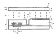
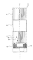
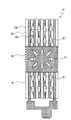
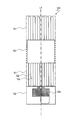
- FIG. 2 is a diagram schematically illustrating a liquid crystal display device 100 according to an embodiment of the present invention, and is a cross-sectional view taken along line 2A-2A ′ in FIG. 1. It is a top view which shows typically the upper layer electrode 12 with which the liquid crystal display device 100 of embodiment by this invention is provided.
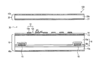
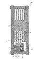
- FIG. 2 is a diagram schematically illustrating a liquid crystal display device 100 according to an embodiment of the present invention, and is a cross-sectional view taken along line 4A-4A ′ in FIG. 1.
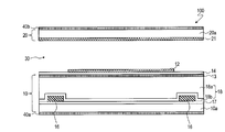
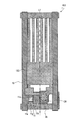
- FIG. 2 is a diagram schematically illustrating a liquid crystal display device 100 according to an embodiment of the present invention, and is a cross-sectional view taken along line 5A-5A ′ in FIG. 1. It is a figure which shows typically the orientation state of the liquid crystal molecule 31 when a voltage is applied to the liquid crystal layer 30 with which the liquid crystal display device 100 of embodiment by this invention is provided. It is a top view which shows typically one pixel of the liquid crystal display device 1000 of a comparative example. It is a top view which shows typically upper layer electrode 12 'with which the liquid crystal display device 1000 of a comparative example is provided.
- FIG. 6 is a diagram showing the result of simulating the alignment state and light transmittance of liquid crystal molecules 31 when a voltage is applied in the device 100. It is a top view which shows typically one pixel of the liquid crystal display device 200 of embodiment by this invention. It is a top view which shows typically upper layer electrode 12A with which the liquid crystal display device 200 of embodiment by this invention is provided. It is a top view which shows typically one pixel of the liquid crystal display device 200 of embodiment by this invention.
- FIG. 1 is a plan view schematically showing one pixel of the liquid crystal display device 100
- FIG. 2 is a cross-sectional view taken along line 2A-2A ′ in FIG.
- the liquid crystal display device 100 includes an active matrix substrate (hereinafter referred to as “TFT substrate”) 10, a counter substrate 20 facing the TFT substrate 10, and a liquid crystal layer 30 provided between the TFT substrate 10 and the counter substrate 20. Is provided.
- TFT substrate active matrix substrate
- counter substrate 20 facing the TFT substrate
- liquid crystal layer 30 provided between the TFT substrate 10 and the counter substrate 20. Is provided.
- the TFT substrate 10 has a thin film transistor (TFT) 11 provided in each of a plurality of pixels.
- the TFT 11 includes a semiconductor layer 11a, a gate electrode 11g, a source electrode 11s, and a drain electrode 11d. In the present embodiment, only one TFT 11 is provided for each pixel.
- the TFT substrate 10 includes an upper layer electrode (first electrode) 12 electrically connected to the drain electrode 11d of the TFT 11, a lower layer electrode (second electrode) 13 provided below the upper layer electrode 12, and an upper layer electrode. 12 and a dielectric layer 14 provided between the lower electrode 13 and the lower layer electrode 13. Different potentials are applied to the upper layer electrode 12 and the lower layer electrode 13.
- the upper layer electrode 12 and the lower layer electrode 13 are each formed from a transparent conductive material (for example, ITO). When viewed from the normal direction of the display surface, the upper layer electrode 12 overlaps at least a part of the lower layer electrode 13 via the dielectric layer 14, and the upper layer electrode 12, the dielectric layer 14, and the lower layer electrode 13 constitute an auxiliary capacitance. To do.
- the TFT substrate 10 further has a scanning wiring (gate bus line) 15 extending substantially parallel to the row direction and a signal wiring (source bus line) 16 extending substantially parallel to the column direction.
- the scanning wiring 15 is electrically connected to the gate electrode 11 g of the TFT 11 and supplies a scanning signal to the TFT 11.
- the signal wiring 16 is electrically connected to the source electrode 11 s of the TFT 11 and supplies a display signal to the TFT 11.
- the above-described components of the TFT substrate 10 are supported by a transparent insulating substrate (for example, a glass substrate) 10a.
- a gate electrode 11g and a scanning wiring 15 of the TFT 11 are provided on the surface of the insulating substrate 10a on the liquid crystal layer 30 side, and a gate insulating layer 17 is formed so as to cover them.
- a semiconductor layer 11 a that functions as a channel region, a source region, and a drain region of the TFT 11 is provided on the gate insulating layer 17.
- various known semiconductor materials can be used. For example, amorphous silicon, polycrystalline silicon, continuous grain boundary crystal silicon (CGS), or the like can be used.
- the semiconductor layer 11a may be an oxide semiconductor layer.
- the oxide semiconductor layer includes, for example, an In—Ga—Zn—O-based semiconductor.
- the In—Ga—Zn—O-based semiconductor may be amorphous or crystalline.
- a semiconductor in which the c-axis is oriented substantially perpendicular to the layer surface is preferable.
- Such a crystal structure of an In—Ga—Zn—O-based semiconductor is disclosed in, for example, Japanese Patent Laid-Open No. 2012-134475.
- Japanese Patent Laid-Open No. 2012-134475 the entire disclosure of Japanese Patent Application Laid-Open No. 2012-134475 is incorporated herein by reference.
- a TFT having an In—Ga—Zn—O-based semiconductor layer has high mobility (more than 20 times that of an a-Si TFT) and low leakage current (less than one hundredth of that of an a-Si TFT).
- the oxide semiconductor layer is not limited to the In—Ga—Zn—O-based semiconductor layer.
- the oxide semiconductor layer includes, for example, a Zn—O based semiconductor (ZnO), an In—Zn—O based semiconductor (IZO), a Zn—Ti—O based semiconductor (ZTO), a Cd—Ge—O based semiconductor, a Cd—Pb—
- ZnO Zn—O based semiconductor
- IZO In—Zn—O based semiconductor
- ZTO Zn—Ti—O based semiconductor
- Cd—Ge—O based semiconductor a Cd—Pb—
- An O-based semiconductor, an In—Sn—Zn—O-based semiconductor (eg, In 2 O 3 —SnO 2 —ZnO), an In—Ga—Sn—O-based semiconductor, or the like may be included.
- a source electrode 11s and a drain electrode 11d are provided in contact with the source region and the drain region of the semiconductor layer 11a.
- a signal wiring 16 is also provided on the gate insulating layer 17.
- An interlayer insulating layer 18 is provided so as to cover the TFT 11 and the signal wiring 16.
- the interlayer insulating layer 18 has a laminated structure including an inorganic insulating film 18a and an organic insulating film 18b formed on the inorganic insulating film 18a.
- the organic insulating film 18b is made of, for example, a photosensitive resin.
- the interlayer insulating layer 18 may be a single layer.
- the lower layer electrode 13 is provided on the interlayer insulating layer 18, and the dielectric layer 14 is formed so as to cover the lower layer electrode 13.
- An upper layer electrode 12 is provided on the dielectric layer 14.
- a contact hole CH exposing a part of the drain electrode 11d is formed.
- the upper layer electrode 12 (more specifically, a third region R3 described later) is electrically connected to the drain electrode 11d.
- the counter substrate 20 has a counter electrode (third electrode) 21 facing the upper layer electrode 12.
- the counter electrode 21 is typically a common electrode provided in common for all pixels.
- the counter electrode 21 is made of a transparent conductive material (for example, ITO).
- the counter substrate 20 typically further includes a color filter and a light shielding layer (black matrix).
- the scanning wiring 15, signal wiring 16, TFT 11, contact hole CH, etc. of the TFT substrate 10 are shielded from light by the light shielding layer.
- the components of the counter electrode 21 (such as the counter electrode 21) are supported by a transparent insulating substrate (for example, a glass substrate) 20a.
- the liquid crystal layer 30 is a vertical alignment type liquid crystal layer. That is, the liquid crystal molecules 31 included in the liquid crystal layer 30 are substantially perpendicular to the substrate surface (typically 85 ° or more as shown in FIG. 2) when no voltage is applied to the liquid crystal layer 30. Orient (to make a corner). Although not shown here, at least one (typically both) of the TFT substrate 10 and the counter substrate 20 has a vertical alignment film provided in contact with the liquid crystal layer 30.
- the orientation maintaining layer may be formed by the PSA technique disclosed in Patent Documents 2 and 3.
- the alignment maintaining layer is provided between the vertical alignment film and the liquid crystal layer 30 and defines the pretilt orientation of the liquid crystal molecules 31 when no voltage is applied to the liquid crystal layer 30.
- the orientation maintaining layer is composed of a photopolymer.
- the photopolymerized material constituting the alignment maintaining layer photopolymerizes a photopolymerizable compound (typically photopolymerizable monomer) added to the liquid crystal material in a voltage applied state (for example, photopolymerization by ultraviolet irradiation). Can be formed.
- the liquid crystal display device 100 further includes a pair of polarizing plates 40 a and 40 b that face each other with the liquid crystal layer 30 interposed therebetween.
- the polarizing plates 40 a and 40 b are provided outside the pair of substrates 10 and 20.
- the polarizing plates 40 a and 40 b are arranged so that a normally black mode display can be performed in combination with the vertically aligned liquid crystal layer 30.
- the polarizing plates 40a and 40b are linear polarizing plates
- the polarizing plates 40a and 40b are arranged so that the polarization axes (transmission axis or absorption axis) are substantially orthogonal to each other (crossed Nicols arrangement).
- the polarizing plates 40a and 40b may be circular polarizing plates.
- FIG. 3 is a plan view showing only the upper layer electrode 12 of the liquid crystal display device 100 of the present embodiment.
- 4 and 5 are cross-sectional views taken along lines 4A-4A 'and 5A-5A' in FIG. 1, respectively.
- the upper layer electrode 12 has a first region R1 and a second region R2 having different electrode structures.
- the upper layer electrode 12 has a third region R3 for electrically connecting the first region R1 and the second region R2 to the drain electrode 11d.
- a plurality of slits (portions from which the conductive film has been removed) 12s are formed in the first region R1 of the upper electrode 12 as shown in FIGS.
- the first region R1 has a plurality of branch portions 12b extending substantially parallel to each other, and each slit 12s is located between two adjacent branch portions 12b.
- the first region R1 has a comb-like electrode structure.
- the first region R1 is also referred to as a “slit formation region”.
- the second region R2 has a planar (that is, solid) electrode structure.
- the second region R2 is also referred to as a “slit non-formation region” or a “solid region”.
- first regions R1 across the second region R2 located in the center of the pixel.
- first region R1 and the first region R1 The number and arrangement of the two regions R2 are not limited to this.
- the third region R3 of the upper layer electrode 12 is continuous with the first region R1. That is, the third region R3 is physically connected to the first region R1. A more specific structure of the third region R3 will be described in detail later.
- the lower layer electrode 13 is formed so that the conductive film is present over almost the whole of the pixel (excluding the portion on the TFT 11 and the vicinity of the contact hole CH). That is, the lower layer electrode 13 is a substantially solid electrode.
- the structure of the lower layer electrode 13 is not limited to this, but it is preferable that the lower layer electrode 13 overlaps at least a part of the slit 12s of the upper layer electrode 12 in order to form a lateral electric field described later. .
- the upper layer electrode 12 is electrically connected to the drain electrode 11d of the TFT 11, a potential corresponding to the display signal supplied from the signal wiring 16 is applied.
- a potential different from that applied to the upper electrode 12 is applied to the lower electrode 13.
- the lower electrode 13 is supplied with the same potential as that applied to the counter electrode 21.
- the first region (slit forming region) R1 and the second region (non-slit forming region, solid region) R2 of the upper electrode 12 have different electrode structures.
- the electric field generated in the liquid crystal layer 30 on the first region R1 and the electric field generated on the liquid crystal layer 30 on the second region R2 have different directions and / or strengths.
- a vertical electric field corresponding to the potential difference between the upper layer electrode 12 and the counter electrode 21 is formed in the liquid crystal layer 30 on the second region R2, whereas the liquid crystal layer 30 on the first region R1
- a horizontal electric field corresponding to the potential difference between the upper layer electrode 12 and the lower layer electrode 13 is also formed.
- the voltage-transmittance (VT) characteristic of the region corresponding to the first region R1 (a relatively dark dark region) is Therefore, the voltage-transmittance (VT) characteristic of the region corresponding to the second region R2 (a relatively bright bright region) is shifted to a higher voltage side.
- FIG. 6 schematically shows the alignment state of the liquid crystal molecules 31 when a voltage is applied to the liquid crystal layer 30.
- the liquid crystal molecules 31 are aligned substantially parallel to the plurality of slits 12s (that is, also to the plurality of branch portions 12b).
- the alignment azimuth differs by approximately 180 ° between the liquid crystal layer 30 on the first region R1 located above the pixel and the liquid crystal layer 30 on the first region R1 located below the pixel.
- the liquid crystal molecules 31 are aligned radially (that is, almost in all directions).
- the liquid crystal display device 100 when a pixel displays a predetermined halftone, two types of regions having different luminances are formed in the pixel, and the voltage-transmittance ( Two types of regions having different (VT) characteristics are formed. Therefore, the viewing angle dependency of the ⁇ characteristic can be improved. Further, in the liquid crystal display device 100 of this embodiment, since it is not necessary to provide a plurality of TFTs 11 for each pixel, the aperture ratio and light transmittance in each pixel can be sufficiently increased. As described above, the liquid crystal display device 100 according to the present embodiment is excellent in viewing angle characteristics, and each pixel has a sufficiently high light transmittance.
- the ratio of the area of the first region R1 (here, the total of the two first regions R1) to the area of the second region R2 is 5: 1. It is preferably ⁇ 1: 2, more preferably 3: 1 to 1: 1.
- the width w1 of the branch part 12b in the first region R1 is preferably 2.0 ⁇ m or more and 8.0 ⁇ m or less
- the width w2 of the slit 12s is preferably 2.0 ⁇ m or more and 8.0 ⁇ m or less.
- the ratio (w1 / w2) of the width w1 of the branch part 12b to the width w2 of the slit 12s is preferably 0.4 or more and 3.0 or less, and more preferably 0.5 or more and 1.5 or less. .
- WO 2012/090773 is a liquid crystal display device having an upper electrode and a lower electrode on the TFT substrate side and a counter electrode on the counter substrate side.
- a liquid crystal display device in which two types of regions having different structures (referred to as “slit region” and “planar region” in the above application) are proposed is proposed.
- the entire disclosure of WO 2012/090773 is incorporated herein by reference.
- the region for electrically connecting the slit region and the planar region to the TFT (the region near the TFT and the contact hole, the upper layer electrode in the liquid crystal display device 100 of the present embodiment
- the structure of the 12th third region R3) is not specifically studied in detail.
- the region of the upper electrode near the contact hole and on the TFT has a “planar electrode structure”, and a conductive film is formed over the entire region of the upper electrode.
- the conductive film of the upper layer electrode is removed on the TFT. In that case, there is no particular problem as long as the contact hole is located at the center in the left-right direction.
- the contact hole may not be arranged in the center in the left-right direction. For this reason, the slit region and the planar region of the upper electrode are electrically connected to the TFT. Therefore, the conductive film in the region for doing so has a left-right asymmetric shape, which deteriorates the display quality.
- the third region R3 of the upper electrode 12 has a structure described later, which suppresses the deterioration in display quality as described above.
- the structure of the third region R3 of the upper layer electrode 12 of the liquid crystal display device 100 of the present embodiment will be described in comparison with the upper layer electrode 12 'of the liquid crystal display device 1000 of the comparative example shown in FIGS.
- FIG. 7 is a plan view schematically showing one pixel of the liquid crystal display device 1000 of the comparative example
- FIG. 8 is a plan view showing only the upper layer electrode 12 ′ of the liquid crystal display device 1000 of the comparative example.
- each pixel is divided into two adjacent areas along the row direction (that is, divided into two in the left-right direction).
- L1 is considered, as shown in FIGS. 1 and 7, the center of the contact hole CH is at a position deviated from this virtual straight line (hereinafter referred to as “left and right dividing line”) L1.
- the first region R1 and the second region R2 of the upper layer electrode 12 ′ in the liquid crystal display device 1000 of the comparative example are the same as the first region R1 and the second region R2 of the upper layer electrode 12 in the liquid crystal display device 100 of the present embodiment, respectively. It has an electrode structure.
- the third region R3 of the upper layer electrode 12 in the liquid crystal display device 100 of the present embodiment has a symmetrical connection portion 12c that is a conductive film pattern having a shape that is substantially symmetrical with respect to the left-right dividing line L1. Is included. In FIG. 3, only the symmetrical connection portion 12c is hatched for ease of understanding. In the configuration illustrated in FIG. 3, the symmetric connection portion 12c is connected (continuous) to the leftmost branch portion 12b and the rightmost branch portion 12b in the first region R1.
- the third region R3 ′ of the upper layer electrode 12 ′ in the liquid crystal display device 1000 of the comparative example includes a conductive film pattern having a substantially symmetric shape with respect to the left-right dividing line L1, as shown in FIG.
- the conductive film in the third region R3 ′ has a remarkably asymmetric shape that is continuous with only the rightmost branch 12b of the first region R1. Since the upper layer electrode 12 ′ is greatly recessed on the contact hole CH (which is easily inferred from FIG. 2), the third region is separated from the orientation change in the first region R1 and the second region R2 when a voltage is applied. In R3, a change in orientation starts from the liquid crystal molecules 31 on the contact holes CH.
- the conductive film in the third region R3 ′ has a remarkably asymmetric shape, the propagation of the orientation starting from the liquid crystal molecule 31 on the contact hole CH differs between the left and right pixels, and the liquid crystal molecule 31 Since the orientation of is also asymmetrical to the left and right, this adversely affects the display.
- the area of the conductive film in the third region R3 ' is large, the laterally asymmetric alignment regulating force from the third region R3' increases, and thus a desired alignment state may not be obtained.
- the third region R3 of the upper electrode 12 has a symmetrical connection portion (conductive film pattern) 12c having a shape that is substantially symmetrical with respect to the left and right dividing line L1.
- the alignment regulating force on the liquid crystal molecules 31 in the third region R3 is approximately the same on the left and right of the pixel, so that the alignment of the liquid crystal layer 30 approaches to the left-right symmetry and is stabilized.
- FIG. 9A shows the result of simulating the alignment state and light transmittance of the liquid crystal molecules 31 when a voltage is applied in the liquid crystal display device 1000 of the comparative example
- FIG. 9B shows the liquid crystal display device of the present embodiment.
- the result of having simulated the orientation state and light transmittance of the liquid crystal molecule 31 at the time of the voltage application in 100 is shown.
- the pixel length was 28.25 ⁇ m in the horizontal direction (X direction), 84.75 ⁇ m in the vertical direction (Y direction), and the voltage applied to the liquid crystal layer 30 was 5.0V.
- the alignment change starts from the liquid crystal molecules 31 in the vicinity of the contact hole CH, and the conductive film in the lower right conductive film (the third region R3 ′ of the upper electrode 12 ′) is changed. It can be seen that the orientation change propagates on the film. As a result, the liquid crystal molecules 31 in the lower left region of the pixel are not well aligned, and the region is dark.
- the orientation change propagates from both the lower left and lower right of the pixel.
- the liquid crystal molecules 31 in the lower left region of the pixel are also well aligned and the region is bright.
- the third region R3 of the upper layer electrode 12 includes the symmetrical connection portion 12c, so that a symmetrical orientation is realized, and the display quality is improved.
- FIG. 10 is a plan view schematically showing one pixel of the liquid crystal display device 200
- FIG. 11 is a plan view showing only the upper layer electrode 12 ⁇ / b> A of the liquid crystal display device 200.
- the liquid crystal display device 200 of the present embodiment will be described focusing on the differences from the liquid crystal display device 100 of the first embodiment.
- the upper layer electrode 12A of the liquid crystal display device 200 of the present embodiment has a first region R1, a second region R2, and a third region R3, similarly to the upper layer electrode 12 of the liquid crystal display device 100 of the first embodiment.
- the first region R1 and the second region R2 of the upper layer electrode 12A of the liquid crystal display device 200 have the same electrode structure as the first region R1 and the second region R2 of the upper layer electrode 12 of the liquid crystal display device 100 of Embodiment 1, respectively. is doing.
- the third region R3 of the upper layer electrode 12A of the liquid crystal display device 200 has a slightly different electrode structure from the third region R3 of the upper layer electrode 12 of the liquid crystal display device 100 of the first embodiment.
- the symmetrical connection portion 12c of the third region R3 of the upper layer electrode 12 is the leftmost branch portion 12b and the most of the first region R1.
- the symmetrical connection portion 12c of the third region R3 of the upper layer electrode 12A has the first region R1. Is continuous with the two branches 12b located in the center.
- the third region R3 of the upper layer electrode 12A includes the symmetric connection portion 12c that is a conductive film pattern having a substantially symmetric shape with respect to the left and right dividing line L1. For this reason, the alignment regulating force applied to the liquid crystal molecules 31 in the third region R3 is approximately the same on the left and right of the pixel, so that the alignment of the liquid crystal layer 30 approaches left-right symmetry and is stabilized. Therefore, the display quality is improved.
- the symmetrical connection portion 12c of the third region R3 is continuous with the branch portion 12b located in the center of the first region R1, and therefore, the signal wiring 16 of the upper layer electrode 12 is connected to the signal wiring 16 of the upper layer electrode 12. Since the area of the adjacent region is reduced, the parasitic capacitance between the signal wiring 16 and the upper layer electrode 12 can be suppressed.
- the symmetrical connection portion 12c of the third region R3 is continuous with the branch portion 12b located at the left end and the right end in the first region R1, and thus on the same branch portion 12b.
- the alignment direction of the liquid crystal molecules 31 is the same direction, and there is an effect that the alignment direction of the liquid crystal molecules 31 is opposite in a region corresponding to one branch portion 12 and no dark line is generated.
- a connection portion region surrounded by a broken line in the drawing
- the alignment boundary appears as a dark line, and such a dark line appears in a region contributing to display in the pixel, the transmittance is lowered.
- FIG. 13 is a plan view schematically showing one pixel of the liquid crystal display device 300
- FIG. 14 is a plan view showing only the upper layer electrode 12 ⁇ / b> B of the liquid crystal display device 300.
- the liquid crystal display device 300 of the present embodiment will be described focusing on differences from the liquid crystal display device 100 of the first embodiment.
- the upper layer electrode 12 is connected to the TFT 11 located on the lower side thereof.
- the upper layer electrode 12B is connected to the TFT 11 located on the upper side thereof. That is, in the liquid crystal display device 100 according to the first embodiment, each pixel is scanned by the scanning wiring 15 positioned below the pixel, whereas in the liquid crystal display device 300 according to the present embodiment, each pixel is located above the pixel. Scanning is performed by the scanning wiring 15 located.
- the third region R3 of the upper layer electrode 12B is a symmetrical connection that is a conductive film pattern having a shape that is substantially symmetrical with respect to the left-right dividing line L1, as shown in FIG. Part 12c is included.
- the alignment regulating force applied to the liquid crystal molecules 31 in the third region R3 is approximately the same on the left and right of the pixel, so that the alignment of the liquid crystal layer 30 approaches left-right symmetry and is stabilized. Therefore, the display quality is improved.
- FIG. 15 is a plan view schematically showing one pixel of the liquid crystal display device 400
- FIG. 16 is a plan view showing only the upper layer electrode 12C of the liquid crystal display device 400.
- the liquid crystal display device 400 according to the present embodiment will be described focusing on differences from the liquid crystal display device 100 according to the first embodiment.
- the upper layer electrode 12C of the liquid crystal display device 400 of the present embodiment has a first region R1, a second region R2, and a third region R3, similar to the upper layer electrode 12 of the liquid crystal display device 100 of the first embodiment.
- the upper layer electrode 12 has two first regions R1, whereas in the liquid crystal display device 400 of the present embodiment, the upper layer electrode 12C has the first region R1. It has only one. Specifically, the first region R1 is located above the pixel, and the second region R2 is located below it. Therefore, the third region R3 of the upper electrode 13C is continuous (connected) with the second region R2.
- the third region R3 of the upper layer electrode 12C includes the symmetric connection portion 12c that is a conductive film pattern having a substantially symmetric shape with respect to the left and right dividing line L1. For this reason, the alignment regulating force applied to the liquid crystal molecules 31 in the third region R3 is approximately the same on the left and right of the pixel, so that the alignment of the liquid crystal layer 30 approaches left-right symmetry and is stabilized. Therefore, the display quality is improved.
- FIG. 17 is a plan view schematically showing one pixel of the liquid crystal display device 500
- FIG. 18 is a plan view showing only the upper layer electrode 12 ⁇ / b> D of the liquid crystal display device 500.
- the upper layer electrode 12D of the liquid crystal display device 500 also has only one first region R1. Specifically, the second region R2 is located above the pixel and the first region R1 is located below the second region R2. Therefore, the third region R3 of the upper layer electrode 13D is continuous (connected) with the first region R1.
- the third region R3 of the upper layer electrode 12D includes a symmetric connection portion 12c that is a conductive film pattern having a substantially symmetric shape with respect to the left and right dividing line L1. For this reason, the alignment regulating force applied to the liquid crystal molecules 31 in the third region R3 is approximately the same on the left and right of the pixel, so that the alignment of the liquid crystal layer 30 approaches left-right symmetry and is stabilized. Therefore, the display quality is improved.
- the orientation in which the liquid crystal molecules 31 are aligned in the dark region of the pixel is One.
- the upper layer electrodes 12, 12A, and 12B of each pixel have two first regions R1, and the liquid crystal molecules in the dark region of the pixel. There are two orientations in which 31 is oriented. Therefore, from the viewpoint of sufficiently improving the viewing angle characteristics in the dark region, the liquid crystal display devices 100, 200, and 300 of the first and second embodiments are more advantageous.
- FIG. 19 is a plan view schematically showing one pixel of the liquid crystal display device 600
- FIG. 20 is a plan view showing only the upper layer electrode 12E of the liquid crystal display device 600.
- the liquid crystal display device 600 of the present embodiment will be described focusing on differences from the liquid crystal display device 100 of the first embodiment.
- the liquid crystal display device 600 of the present embodiment is different from the liquid crystal display device 100 of the first embodiment in that the upper layer electrode 12E has four first regions R1.
- the upper layer electrode 12E includes two first regions R1 located on the left side and the right side of the second region R2 in addition to the two first regions R1 located above and below the second region R2. .
- the plurality of slits 12s and the plurality of branch portions 12b extend in a direction substantially orthogonal to the plurality of slits 12s and the plurality of branch portions 12b in the former two first regions R1. .
- the liquid crystal molecules 31 on the latter two first regions R1 are aligned in a direction substantially orthogonal to the alignment direction of the liquid crystal molecules 31 on the former two first regions R1.
- the orientation direction of the liquid crystal layer 30 on the first region R1 located on the left side of the second region R2 and the liquid crystal layer 30 on the first region R1 located on the right side of the second region R2 are different by about 180 °. . Therefore, in the liquid crystal display device 600 of the present embodiment, the liquid crystal molecules 31 are aligned in four directions in the dark region of the pixel. Therefore, the viewing angle characteristics can be further improved.
- FIG. 21 is a plan view schematically showing one pixel of the liquid crystal display device 700
- FIG. 22 is a plan view showing only the upper layer electrode 12F of the liquid crystal display device 700.
- the upper layer electrode 12F of the liquid crystal display device 700 also has four first regions R1, and the liquid crystal molecules 31 are aligned in four different directions in the dark region of the pixel.
- the plurality of slits 12s and the plurality of branch portions 12b extend in a direction substantially parallel to or substantially orthogonal to the row direction and the column direction.
- the plurality of slits 12s and the plurality of branches 12b have an angle of about 45 ° with respect to the row direction and the column direction. It extends in the direction of making.
- the areas of the four first regions R1 are substantially equal to each other. Therefore, the effect of improving the viewing angle characteristic is even higher.
- a liquid crystal display device which has excellent viewing angle characteristics and each pixel has a sufficiently high light transmittance.
- the liquid crystal display device according to the embodiment of the present invention can perform high-quality display even when the pixel size is small with high definition.
- TFT substrate 10 Active matrix substrate (TFT substrate) 10a Insulating substrate 11 Thin film transistor (TFT) 11a Semiconductor layer 11g Gate electrode 11s Source electrode 11d Drain electrode 12, 12A, 12B, 12C, 12D, 12E, 12F Upper layer electrode 12b Branch portion 12c Symmetric connection portion 12s Slit 13 Lower layer electrode 14 Dielectric layer 15 Scanning wiring (gate bus line) ) 16 Signal wiring (source bus line) 17 Gate insulating layer 18 Interlayer insulating layer 18a Inorganic insulating film 18b Organic insulating film 20 Counter substrate 20a Insulating substrate 21 Counter electrode 30 Liquid crystal layer 31 Liquid crystal molecule 40a, 40b Polarizer CH Contact hole R1 First region of upper electrode R2 Upper electrode Second region R3 Third region of upper electrode 100, 200, 300, 400 Liquid crystal display device 500, 600, 700 Liquid crystal display device
Landscapes
- Physics & Mathematics (AREA)
- Nonlinear Science (AREA)
- Mathematical Physics (AREA)
- Chemical & Material Sciences (AREA)
- Crystallography & Structural Chemistry (AREA)
- General Physics & Mathematics (AREA)
- Optics & Photonics (AREA)
- Geometry (AREA)
- Engineering & Computer Science (AREA)
- Microelectronics & Electronic Packaging (AREA)
- Liquid Crystal (AREA)
Abstract
液晶表示装置(100)のTFT基板(10)は、各画素に設けられたTFT(11)と、TFTのドレイン電極(11d)に電気的に接続された上層電極(12)と、上層電極の下方に設けられた下層電極(13)と、上層電極および下層電極の間に設けられた誘電体層(14)とを有し、対向基板(20)は、上層電極に対向する対向電極(21)を有する。上層電極は、互いに異なる電極構造を有する第1領域(R1)および第2領域(R2)と、第1領域および第2領域をドレイン電極に電気的に接続するための第3領域(R3)とを有する。上層電極の第3領域は、各画素を行方向に沿って隣接する2つの領域に分割する仮想的な直線(L1)に対して実質的に対称な形状を有する導電膜パターンである対称接続部(12c)を含む。
Description
本発明は、液晶表示装置に関する。
液晶表示装置の表示特性が改善され、テレビジョン受像機などへの利用が進んでいる。液晶表示装置の視野角特性は向上したものの、さらなる改善が望まれている。特に、垂直配向型の液晶層を用いた液晶表示装置の視野角特性を改善する要求は強い。垂直配向型液晶層を備えた液晶表示装置は、VA(Vertical Alignment)モードの液晶表示装置と呼ばれる。
現在、テレビ等の大型表示装置に用いられているVAモードの液晶表示装置には、視野角特性を改善するために、1つの画素に複数の液晶ドメインを形成する配向分割構造が採用されている。配向分割構造を形成する方法としては、MVA(Multi-domain Vertical Alignment)モードが主流である。MVAモードは、例えば特許文献1に開示されている。
MVAモードでは、垂直配向型液晶層を挟んで対向する一対の基板のそれぞれの液晶層側に配向規制構造を設けることによって、各画素内に配向方向(チルト方向)が異なる複数の液晶ドメイン(典型的には配向方向は4種類)が形成される。配向規制構造としては、電極に形成されたスリット(開口部)や、リブ(突起構造)が用いられ、液晶層の両側から配向規制力が発揮される。
しかしながら、スリットやリブを用いると、従来のTN(Twisted Nematic)モードで用いられていた配向膜によってプレチルト方向を規定した場合と異なり、スリットやリブが線状であることから、液晶分子に対する配向規制力が画素内で不均一となるため、応答速度に分布が生じるという問題がある。
MVAモードの応答特性を改善する目的で、PSA技術(Polymer Sustained Alignment Technology)が開発されている。PSA技術は、例えば特許文献2および3に開示されている。PSA技術では、液晶分子にプレチルトを付与するために、配向維持層と呼ばれるポリマー層が用いられる。配向維持層は、液晶材料に予め混合しておいた光重合性モノマーを、液晶セルを作製した後、液晶層に電圧が印加された状態で重合することによって形成される。モノマーを重合するときに印加される電界の分布および強度を調整することによって、液晶分子のプレチルト方位(基板面内の方位角)およびプレチルト角(基板面からの立ち上がり角)を制御することができる。
また、特許文献3には、PSA技術とともに微細なストライプ状パターンを有する画素電極(「フィッシュボーン型画素電極」と呼ばれることもある)を用いた構成が開示されている。この構成では、液晶層に電圧を印加すると、液晶分子はストライプ状パターンの長手方向に平行に配向する。これは、特許文献1に記載されている従来のMVAモードではスリットやリブなどの直線状の配向規制構造に対して直交する方向に液晶分子が配向するのとは対照的である。微細なストライプ状パターンのライン&スペースは、従来のMVAモードの配向規制構造の幅よりも小さくてよい。従って、フィッシュボーン型画素電極は、従来のMVAモードの配向規制構造よりも小型の画素に適用しやすいという利点を有する。
上述したようなVAモードの改良技術(PSA技術やフィッシュボーン型画素電極)によれば、高い視野角特性を実現することができる。しかしながら、近年、VAモードの液晶表示装置の視野角特性のさらなる改善が望まれており、そのために「画素分割駆動技術」が実用化されている(例えば特許文献4および5)。
画素分割駆動技術によれば、正面方向から観測したときのγ(ガンマ)特性と斜め方向から観測したときのγ特性とが異なるという問題点、すなわち、γ特性の視角依存性が改善される。ここで、γ特性とは、表示輝度の階調依存性である。
画素分割駆動技術では、1つの画素を、互いに異なる電圧を液晶層に印加し得る、つまり、互いに異なる輝度を呈し得る複数の副画素で構成し、画素に入力される表示信号電圧に対応する所定の輝度を、1つの画素全体で実現する。つまり、画素分割駆動技術とは、複数の副画素の互いに異なるγ特性を合成することによって、画素のγ特性の視角依存性を改善する技術である。
しかしながら、画素分割駆動技術を用いる場合、液晶層への実効的な印加電圧を副画素ごとに異ならせる必要があるので、各画素に設けられる画素電極は、複数の副画素に対応した複数の副画素電極を有しており、それぞれの副画素電極に対応してスイッチング素子(例えばTFT)が設けられる。このように、各画素に少なくとも2つのスイッチング素子が設けられるので、各画素の開口率および光透過率が低減してしまう。開口率および光透過率の低減は、1画素の面積が小さくなる高精細な液晶表示装置において特に顕著である。
本発明は、上記問題に鑑みてなされたものであり、その目的は、視野角特性に優れ、且つ、各画素が十分に高い光透過率を有する液晶表示装置を提供することにある。
本発明による実施形態の液晶表示装置は、アクティブマトリクス基板と、前記アクティブマトリクス基板に対向する対向基板と、前記アクティブマトリクス基板および前記対向基板の間に設けられた液晶層と、を備え、複数の行および複数の列を含むマトリクス状に配置された複数の画素を有する液晶表示装置であって、前記アクティブマトリクス基板は、前記複数の画素のそれぞれに設けられ、ゲート電極、ソース電極およびドレイン電極を有する薄膜トランジスタと、前記薄膜トランジスタの前記ドレイン電極に電気的に接続された上層電極と、前記上層電極の下方に設けられた下層電極と、前記上層電極および前記下層電極の間に設けられた誘電体層と、を有し、前記対向基板は、前記上層電極に対向する対向電極を有し、前記上層電極は、互いに異なる電極構造を有する第1領域および第2領域と、前記第1領域および前記第2領域を前記ドレイン電極に電気的に接続するための第3領域とを有し、前記上層電極の前記第3領域は、各画素を行方向に沿って隣接する2つの領域に分割する仮想的な直線に対して実質的に対称な形状を有する導電膜パターンである対称接続部を含む。
ある実施形態において、前記アクティブマトリクス基板は、前記薄膜トランジスタを覆うように設けられた層間絶縁層をさらに有し、前記層間絶縁層および前記誘電体層には、前記ドレイン電極の一部を露出するコンタクトホールであって、その中で前記ドレイン電極に前記上層電極の前記第3領域が電気的に接続されるコンタクトホールが形成されており、前記コンタクトホールの中心は、前記仮想的な直線からずれた位置にある。
ある実施形態において、前記アクティブマトリクス基板は、行方向に略平行に延設され、前記薄膜トランジスタの前記ゲート電極に電気的に接続された走査配線と、列方向に略平行に延設され、前記薄膜トランジスタの前記ソース電極に電気的に接続された信号配線と、をさらに有する。
ある実施形態において、前記液晶層に電圧が印加されたとき、前記上層電極の前記第1領域上の前記液晶層に生成される電界と、前記上層電極の前記第2領域上の前記液晶層に生成される電界とは、向きおよび/または強さが異なる。
ある実施形態において、前記複数の画素のうちのある画素が所定の中間調を表示するとき、前記ある画素の、前記上層電極の前記第1領域に対応する領域の輝度は、前記ある画素の、前記上層電極の前記第2領域に対応する領域の輝度よりも低い。
ある実施形態において、前記上層電極の前記第1領域には、複数のスリットが形成されており、前記上層電極の前記第2領域には、スリットが形成されていない。
ある実施形態において、前記液晶層に電圧が印加されたとき、前記上層電極の前記第1領域上の前記液晶層において、液晶分子は前記複数のスリットに略平行に配向し、前記上層電極の前記第2領域上の前記液晶層において、液晶分子は放射状に配向する。
ある実施形態において、前記上層電極の前記第3領域は、前記第1領域と連続している。
ある実施形態において、前記上層電極の前記第3領域は、前記第2領域と連続している。
ある実施形態において、前記液晶層は、垂直配向型の液晶層である。
ある実施形態において、前記アクティブマトリクス基板および前記対向基板の少なくとも一方は、垂直配向膜と、前記垂直配向膜および前記液晶層の間に設けられた配向維持層であって、前記液晶層に電圧が印加されていないときに液晶分子のプレチルト方位を規定する配向維持層と、を有する。
ある実施形態において、前記上層電極および前記下層電極には、互いに異なる電位が与えられる。
ある実施形態において、前記上層電極および前記下層電極は、それぞれ透明な導電材料から形成されている。
ある実施形態において、前記上層電極は、表示面法線方向から見たとき、前記誘電体層を介して前記下層電極の少なくとも一部に重なり、前記上層電極、前記誘電体層および前記下層電極は、補助容量を構成する。
ある実施形態において、本発明による液晶表示装置は、前記液晶層を介して互いに対向する一対の偏光板をさらに備える。
ある実施形態において、前記薄膜トランジスタは、酸化物半導体層を有する。
ある実施形態において、前記酸化物半導体層は、In-Ga-Zn-O系の半導体を含む。
本発明の実施形態によれば、視野角特性に優れ、且つ、各画素が十分に高い光透過率を有する液晶表示装置が提供される。
以下、図面を参照しながら本発明の実施形態を説明する。なお、本発明は以下の実施形態に限定されるものではない。
(実施形態1)
図1および図2に、本実施形態における液晶表示装置100を示す。液晶表示装置100は、複数の行および複数の列を含むマトリクス状に配置された複数の画素を有している。図1は、液晶表示装置100の1つの画素を模式的に示す平面図であり、図2は、図1中の2A-2A’線に沿った断面図である。
図1および図2に、本実施形態における液晶表示装置100を示す。液晶表示装置100は、複数の行および複数の列を含むマトリクス状に配置された複数の画素を有している。図1は、液晶表示装置100の1つの画素を模式的に示す平面図であり、図2は、図1中の2A-2A’線に沿った断面図である。
液晶表示装置100は、アクティブマトリクス基板(以下では「TFT基板」と称する)10と、TFT基板10に対向する対向基板20と、TFT基板10および対向基板20の間に設けられた液晶層30とを備える。
TFT基板10は、複数の画素のそれぞれに設けられた薄膜トランジスタ(TFT)11を有する。TFT11は、半導体層11aと、ゲート電極11g、ソース電極11sおよびドレイン電極11dとを有する。本実施形態では、各画素にTFT11が1つだけ設けられている。
また、TFT基板10は、TFT11のドレイン電極11dに電気的に接続された上層電極(第1電極)12と、上層電極12の下方に設けられた下層電極(第2電極)13と、上層電極12および下層電極13の間に設けられた誘電体層14とを有する。上層電極12および下層電極13には、互いに異なる電位が与えられる。上層電極12および下層電極13は、それぞれ透明な導電材料(例えばITO)から形成されている。上層電極12は、表示面法線方向から見たとき、誘電体層14を介して下層電極13の少なくとも一部に重なり、上層電極12、誘電体層14および下層電極13は、補助容量を構成する。
TFT基板10は、さらに、行方向に略平行に延設された走査配線(ゲートバスライン)15と、列方向に略平行に延設された信号配線(ソースバスライン)16とを有する。走査配線15は、TFT11のゲート電極11gに電気的に接続されており、TFT11に走査信号を供給する。信号配線16は、TFT11のソース電極11sに電気的に接続されており、TFT11に表示信号を供給する。
上述したTFT基板10の構成要素は、透明な絶縁性基板(例えばガラス基板)10aによって支持されている。絶縁性基板10aの液晶層30側の表面上に、TFT11のゲート電極11gおよび走査配線15が設けられており、これらを覆うようにゲート絶縁層17が形成されている。
ゲート絶縁層17上に、TFT11のチャネル領域、ソース領域およびドレイン領域として機能する半導体層11aが設けられている。半導体層11aの材料としては、公知の種々の半導体材料を用いることができ、例えば、アモルファスシリコン、多結晶シリコン、連続粒界結晶シリコン(CGS:Continuous Grain Silicon)などを用いることができる。
また、半導体層11aは、酸化物半導体層であってもよい。酸化物半導体層は、例えばIn-Ga-Zn-O系の半導体を含む。ここで、In-Ga-Zn-O系半導体は、In(インジウム)、Ga(ガリウム)、Zn(亜鉛)の三元系酸化物であって、In、GaおよびZnの割合(組成比)は特に限定されず、例えばIn:Ga:Zn=2:2:1、In:Ga:Zn=1:1:1、In:Ga:Zn=1:1:2等を含む。In-Ga-Zn-O系半導体は、アモルファスでもよいし、結晶質でもよい。結晶質のIn-Ga-Zn-O系半導体としては、c軸が層面に概ね垂直に配向したものが好ましい。このようなIn-Ga-Zn-O系半導体の結晶構造は、例えば、特開2012-134475号公報に開示されている。参考のために、特開2012-134475号公報の開示内容の全てを本明細書に援用する。In-Ga-Zn-O系半導体層を有するTFTは、高い移動度(a-SiTFTに比べ20倍超)および低いリーク電流(a-SiTFTに比べ100分の1未満)を有している。
なお、酸化物半導体層は、In-Ga-Zn-O系半導体層に限定されない。酸化物半導体層は、例えばZn-O系半導体(ZnO)、In-Zn-O系半導体(IZO)、Zn-Ti-O系半導体(ZTO)、Cd-Ge-O系半導体、Cd-Pb-O系半導体、In―Sn―Zn―O系半導体(例えばIn2O3-SnO2-ZnO)、In-Ga-Sn-O系半導体などを含んでいてもよい。
半導体層11aのソース領域およびドレイン領域に接するように、ソース電極11sおよびドレイン電極11dが設けられている。また、ゲート絶縁層17上には、信号配線16も設けられている。
TFT11や信号配線16を覆うように、層間絶縁層18が設けられている。本実施形態では、層間絶縁層18は、無機絶縁膜18aと、無機絶縁膜18a上に形成された有機絶縁膜18bとを含む積層構造を有している。有機絶縁膜18bは、例えば感光性樹脂から形成されている。勿論、層間絶縁層18は単層であってもよい。
層間絶縁層18上に、下層電極13が設けられており、下層電極13を覆うように、誘電体層14が形成されている。誘電体層14上に、上層電極12が設けられている。層間絶縁層18および誘電体層14には、ドレイン電極11dの一部を露出するコンタクトホールCHが形成されている。コンタクトホールCHの中で、ドレイン電極11dに上層電極12が(より具体的には後述する第3領域R3が)電気的に接続されている。
対向基板20は、上層電極12に対向する対向電極(第3電極)21を有する。対向電極21は、典型的には、すべての画素に共通に設けられた共通電極である。対向電極21は、透明な導電材料(例えばITO)から形成されている。なお、ここでは図示していないが、対向基板20は、典型的には、カラーフィルタおよび遮光層(ブラックマトリクス)をさらに有する。TFT基板10の走査配線15、信号配線16、TFT11、コンタクトホールCHなどは、遮光層によって遮光されている。対向電極21の構成要素(対向電極21など)は、透明な絶縁性基板(例えばガラス基板)20aによって支持されている。
液晶層30は、垂直配向型の液晶層である。つまり、液晶層30に含まれる液晶分子31は、液晶層30に電圧が印加されていない状態において、図2に示すように、基板面に対して略垂直に(典型的には85°以上の角をなすように)配向する。なお、ここでは図示していないが、TFT基板10および対向基板20の少なくとも一方(典型的には両方)は、液晶層30に接するように設けられた垂直配向膜を有する。
なお、特許文献2および3に開示されているようなPSA技術により、配向維持層を形成してもよい。配向維持層は、垂直配向膜および液晶層30の間に設けられ、液晶層30に電圧が印加されていないときに液晶分子31のプレチルト方位を規定する。配向維持層は、光重合物から構成される。配向維持層を構成する光重合物は、液晶材料中に添加されている光重合性化合物(典型的には光重合性モノマー)を、電圧印加状態で光重合(例えば紫外線照射による光重合)することによって形成することができる。
また、液晶表示装置100は、液晶層30を介して互いに対向する一対の偏光板40aおよび40bをさらに備える。図2に例示している構成では、偏光板40aおよび40bは、一対の基板10および20の外側に設けられている。偏光板40aおよび40bは、垂直配向型の液晶層30と組み合わせてノーマリブラックモードの表示を行い得るように、配置されている。例えば偏光板40aおよび40bが直線偏光板である場合には、偏光板40aおよび40bは、偏光軸(透過軸または吸収軸)が互いに略直交するように配置されている(クロスニコル配置)。勿論、偏光板40aおよび40bは、円偏光板であってもよい。
ここで、図3、図4および図5も参照しながら、TFT基板10が有する上層電極12および下層電極13の構造をより具体的に説明する。図3は、本実施形態の液晶表示装置100の上層電極12のみを示す平面図である。図4および図5は、それぞれ図1中の4A-4A’線および5A-5A’線に沿った断面図である。
上層電極12は、互いに異なる電極構造を有する第1領域R1および第2領域R2を有する。また、上層電極12は、第1領域R1および第2領域R2をドレイン電極11dに電気的に接続するための第3領域R3を有する。
本実施形態では、上層電極12の第1領域R1には、図3および図4に示すように、複数のスリット(導電膜が除去された部分)12sが形成されている。第1領域R1は、互いに略平行に延びる複数の枝部12bを有し、隣接する2つの枝部12b間に、各スリット12sが位置している。このように、第1領域R1は、櫛歯状の電極構造を有する。以下では、第1領域R1を「スリット形成領域」とも呼ぶ。
これに対し、上層電極12の第2領域R2には、図3および図5に示すように、スリットは形成されていない。つまり、第2領域R2は、面状の(つまりべた)電極構造を有する。以下では、第2領域R2を「スリット非形成領域」、あるいは、「べた領域」とも呼ぶ。
なお、図3などに例示している構成では、画素の中央に位置する第2領域R2を挟んで2つの第1領域R1が存在しているが、後述するように、第1領域R1および第2領域R2の個数や配置はこれに限定されるものではない。
上層電極12の第3領域R3は、図3などに例示している構成では、第1領域R1と連続している。つまり、第3領域R3は、第1領域R1に物理的に接続されている。第3領域R3のより具体的な構造については、後に詳述する。
下層電極13は、画素内のほぼ全体(TFT11上やコンタクトホールCH近傍を除く部分)にわたって導電膜が存在するように形成されている。つまり、下層電極13は、ほぼべた電極である。勿論、下層電極13の構造はこれに限定されるものではないが、後述する横電界を形成するために、下層電極13は、上層電極12のスリット12sの少なくとも一部に重なっていることが好ましい。
上層電極12は、TFT11のドレイン電極11dに電気的に接続されているので、信号配線16から供給される表示信号に対応した電位を与えられる。これに対し、下層電極13には、上層電極12に与えられる電位とは異なる電位が与えられる。典型的には、下層電極13には、対向電極21に与えられる電位と同じ電位が与えられる。
上述したように、上層電極12の第1領域(スリット形成領域)R1と第2領域(スリット非形成領域、べた領域)R2とは、互いに異なる電極構造を有しているので、液晶層30に電圧が印加されたとき、第1領域R1上の液晶層30に生成される電界と、第2領域R2上の液晶層30に生成される電界とは、向きおよび/または強さが異なる。具体的には、第2領域R2上の液晶層30には、上層電極12と対向電極21との電位差に応じた縦電界が形成されるのに対し、第1領域R1上の液晶層30には、上層電極12と対向電極21との電位差に応じた縦電界に加え、上層電極12と下層電極13との電位差に応じた横電界も形成される。
このように、第1領域R1上の液晶層30には縦電界だけでなく横電界も形成されるので、第1領域R1上の液晶層30においては、第2領域R2上の液晶層30においてよりも、液晶分子31の傾斜する程度が低くなる。従って、ある画素が所定の中間調を表示するとき、その画素の第1領域R1に対応する領域の輝度は、その画素の第2領域R2に対応する領域の輝度よりも低くなる。つまり、画素内に、互いに輝度の異なる2種類の領域が形成されることになり、第1領域R1に対応する領域(相対的に暗い暗領域)の電圧-透過率(V-T)特性は、第2領域R2に対応する領域(相対的に明るい明領域)の電圧-透過率(V-T)特性よりも高電圧側にシフトすることになる。
図6に、液晶層30に電圧が印加されたときの液晶分子31の配向状態を模式的に示す。上層電極12の第1領域R1上の液晶層30において、図6に示すように、液晶分子31は、複数のスリット12sに(つまり複数の枝部12bにも)略平行に配向する。ただし、画素の上側に位置する第1領域R1上の液晶層30と、画素の下側に位置する第1領域R1上の液晶層30とでは、配向方位は略180°異なる。これに対し、上層電極12の第2領域R2上の液晶層30においては、液晶分子31は、放射状に(つまりほぼ全方位に)配向する。
上述したように、本実施形態における液晶表示装置100では、ある画素が所定の中間調を表示するとき、画素内に互いに輝度の異なる2種類の領域が形成され、画素内に電圧-透過率(V-T)特性の異なる2種類の領域が形成されることになる。そのため、γ特性の視角依存性を改善することができる。また、本実施形態の液晶表示装置100では、各画素に複数のTFT11を設ける必要がないので、各画素における開口率および光透過率を十分に高くすることができる。このように、本実施形態における液晶表示装置100は、視野角特性に優れ、且つ、各画素が十分に高い光透過率を有する。
なお、γ特性の視角依存性を十分に改善する観点からは、第1領域R1の面積(ここでは2つの第1領域R1の合計)と第2領域R2の面積との比は、5:1~1:2であることが好ましく、3:1~1:1であることがより好ましい。
また、第1領域R1における枝部12bの幅w1は、2.0μm以上8.0μm以下であることが好ましく、スリット12sの幅w2は、2.0μm以上8.0μm以下であることが好ましい。枝部12bの幅w1の、スリット12sの幅w2に対する比(w1/w2)は、0.4以上3.0以下であることが好ましく、0.5以上1.5以下であることがより好ましい。
なお、本願出願人は、国際公開第2012/090773号に、TFT基板側に上層電極および下層電極を備えるとともに対向基板側に対向電極を備える液晶表示装置であって、さらに、上層電極に互いに電極構造の異なる2種類の領域(上記出願では「スリット領域」および「面状領域」と呼ばれている)が形成された液晶表示装置を提案している。上記国際公開第2012/090773号の全ての開示内容を、本明細書に参考のために援用する。
しかしながら、上記出願では、上層電極のうち、スリット領域および面状領域をTFTに電気的に接続するための領域(TFTおよびコンタクトホール近傍の領域であり、本実施形態の液晶表示装置100における上層電極12の第3領域R3に対応)の構造に関しては、特別に詳細な検討がなされているわけではない。例えば、上記出願では、上層電極の、コンタクトホール近傍およびTFT上の領域が「面状電極構造」を有しているとされており、上層電極の当該領域全体に導電膜が形成されている。
ところが、上層電極のTFT上に位置する領域がそのような構造を有していると、TFT特性が変化してしまうことがある。そのため、TFT上においては、上層電極の導電膜が除去されていることが好ましい。その場合、コンタクトホールが左右方向における中央に位置していれば、特に問題はない。しかしながら、高精細な液晶パネルでは、画素サイズが小さいので、コンタクトホールを左右方向における中央に配置できないことがあり、そのために、上層電極のうち、スリット領域および面状領域をTFTに電気的に接続するための領域の導電膜が、左右非対称な形状となってしまい、そのことによって表示品位が低下してしまう。
これに対し、本実施形態における液晶表示装置100では、上層電極12の第3領域R3が後述する構造を有しているので、そのことによって上述したような表示品位の低下が抑制される。以下、図7および図8に示す比較例の液晶表示装置1000の上層電極12’と比較しながら、本実施形態の液晶表示装置100の上層電極12の第3領域R3の構造を説明する。図7は、比較例の液晶表示装置1000の1つの画素を模式的に示す平面図であり、図8は、比較例の液晶表示装置1000の上層電極12’のみを示す平面図である。
本実施形態の液晶表示装置100および比較例の液晶表示装置1000のいずれにおいても、各画素を行方向に沿って隣接する2つの領域に分割する(つまり左右方向に2分割する)仮想的な直線L1を考えたとき、図1および図7に示すように、コンタクトホールCHの中心は、この仮想的な直線(以下では「左右分割線」と呼ぶ)L1からずれた位置にある。
比較例の液晶表示装置1000における上層電極12’の第1領域R1および第2領域R2は、それぞれ、本実施形態の液晶表示装置100における上層電極12の第1領域R1および第2領域R2と同じ電極構造を有している。
本実施形態の液晶表示装置100における上層電極12の第3領域R3は、図3に示すように、左右分割線L1に対して実質的に対称な形状を有する導電膜パターンである対称接続部12cを含んでいる。図3では、理解の容易さのために、対称接続部12cにのみハッチングを付している。図3に例示している構成では、対称接続部12cは、第1領域R1におけるもっとも左側の枝部12bおよびもっとも右側の枝部12bと接続されている(連続している)。
一方、比較例の液晶表示装置1000における上層電極12’の第3領域R3’は、図8に示すように、左右分割線L1に対して実質的に対称な形状を有する導電膜パターンを含んでおらず、第3領域R3’内の導電膜は、第1領域R1のもっとも右側の枝部12bのみと連続するような、著しく左右非対称な形状を有する。上層電極12’は、コンタクトホールCH上で大きく凹む(図2からも容易に類推される)ので、電圧印加時に、第1領域R1および第2領域R2における配向変化とは別途に、第3領域R3では、コンタクトホールCH上の液晶分子31を起点とした配向の変化が開始される。このとき、第3領域R3’内の導電膜が著しく左右非対称な形状を有していると、コンタクトホールCH上の液晶分子31を起点とした配向の伝播が画素の左右で異なり、液晶分子31の配向も著しく左右非対称となるので、そのことが表示に悪影響を与える。また、第3領域R3’における導電膜の面積が大きいと、第3領域R3’からの左右非対称な配向規制力が大きくなり、そのことによって所望の配向状態が得られないこともある。
これに対し、本実施形態の液晶表示装置100のように、上層電極12の第3領域R3が、左右分割線L1に対して実質的に対称な形状を有する対称接続部(導電膜パターン)12cを含んでいると、第3領域R3における液晶分子31への配向規制力が画素の左右で同程度となるので、液晶層30の配向が左右対称に近づき、安定化される。
図9(a)に、比較例の液晶表示装置1000における電圧印加時の液晶分子31の配向状態および光透過率をシミュレーションした結果を示し、図9(b)に、本実施形態の液晶表示装置100における電圧印加時の液晶分子31の配向状態および光透過率をシミュレーションした結果を示す。シミュレーションに際しては、画素の長さを左右方向(X方向)について28.25μm、上下方向(Y方向)について84.75μmとし、液晶層30への印加電圧を5.0Vとした。
図9(a)から、比較例の液晶表示装置1000では、コンタクトホールCH近傍の液晶分子31を起点として配向変化が始まり、右下の導電膜(上層電極12’の第3領域R3’の導電膜)上を配向変化が伝播している様子が分かる。その結果、画素の左下の領域の液晶分子31はうまく配向せず、その領域が暗くなってしまっている。
これに対し、図9(b)から、本実施形態の液晶表示装置100では、画素の左下および右下の両方から配向変化が伝播している様子が分かる。その結果、画素の左下の領域の液晶分子31もうまく配向し、その領域が明るくなっている。
このように、本実施形態の液晶表示装置100では、上層電極12の第3領域R3が対称接続部12cを含んでいることにより、左右対称な配向が実現され、表示品位が向上する。
(実施形態2)
図10および図11を参照しながら、本実施形態における液晶表示装置200を説明する。図10は、液晶表示装置200の1つの画素を模式的に示す平面図であり、図11は、液晶表示装置200の上層電極12Aのみを示す平面図である。以下では、本実施形態の液晶表示装置200が、実施形態1の液晶表示装置100と異なる点を中心に説明を行う。
図10および図11を参照しながら、本実施形態における液晶表示装置200を説明する。図10は、液晶表示装置200の1つの画素を模式的に示す平面図であり、図11は、液晶表示装置200の上層電極12Aのみを示す平面図である。以下では、本実施形態の液晶表示装置200が、実施形態1の液晶表示装置100と異なる点を中心に説明を行う。
本実施形態の液晶表示装置200の上層電極12Aは、実施形態1の液晶表示装置100の上層電極12と同様に、第1領域R1、第2領域R2および第3領域R3を有する。
液晶表示装置200の上層電極12Aの第1領域R1および第2領域R2は、それぞれ、実施形態1の液晶表示装置100の上層電極12の第1領域R1および第2領域R2と同じ電極構造を有している。
これに対し、液晶表示装置200の上層電極12Aの第3領域R3は、実施形態1の液晶表示装置100の上層電極12の第3領域R3とはやや異なる電極構造を有している。具体的には、実施形態1の液晶表示装置100では、図3に示したように、上層電極12の第3領域R3の対称接続部12cが第1領域R1におけるもっとも左側の枝部12bおよびもっとも右側の枝部12bと連続しているのに対し、本実施形態の液晶表示装置200では、図11に示すように、上層電極12Aの第3領域R3の対称接続部12cは、第1領域R1における中央に位置する2つの枝部12bと連続している。
本実施形態の液晶表示装置200においても、上層電極12Aの第3領域R3は、左右分割線L1に対して実質的に対称な形状を有する導電膜パターンである対称接続部12cを含んでいる。そのため、第3領域R3における液晶分子31への配向規制力が画素の左右で同程度となるので、液晶層30の配向が左右対称に近づき、安定化される。それ故、表示品位が向上する。
なお、本実施形態の液晶表示装置200では、第3領域R3の対称接続部12cが第1領域R1における中央に位置する枝部12bと連続しているので、上層電極12の、信号配線16に近接する領域の面積が小さくなるため、信号配線16と上層電極12との間での寄生容量が抑えられるという効果も得られる。一方、実施形態1の液晶表示装置100では、第3領域R3の対称接続部12cが第1領域R1における左端および右端に位置する枝部12bと連続しているので、同一の枝部12b上における液晶分子31の配向方向が同一方向となり、1つの枝部12に対応する領域内で液晶分子31の配向方向が反対になって暗線が生じるということがないという効果が得られる。これに対し、液晶表示装置200では、図12に模式的に示すように、中央に位置する枝部12bと対称接続部12cとの接続部(図中の破線で囲まれた領域)を境として液晶分子31の配向方向が反対になって配向の境界が暗線となって現れ、そのような暗線が画素内の表示に寄与する領域に現れると透過率が下がってしまう。
続いて、図13および図14を参照しながら、本実施形態における他の液晶表示装置300を説明する。図13は、液晶表示装置300の1つの画素を模式的に示す平面図であり、図14は、液晶表示装置300の上層電極12Bのみを示す平面図である。以下では、本実施形態の液晶表示装置300が、実施形態1の液晶表示装置100と異なる点を中心に説明を行う。
実施形態1の液晶表示装置100では、図1に示したように、上層電極12は、その下側に位置するTFT11に接続されている。これに対し、本実施形態の液晶表示装置300では、図13に示すように、上層電極12Bは、その上側に位置するTFT11に接続されている。つまり、実施形態1の液晶表示装置100では、各画素は、その下側に位置する走査配線15によって走査されるのに対し、本実施形態の液晶表示装置300では、各画素は、その上側に位置する走査配線15によって走査される。
本実施形態の液晶表示装置300においても、上層電極12Bの第3領域R3は、図14に示すように、左右分割線L1に対して実質的に対称な形状を有する導電膜パターンである対称接続部12cを含んでいる。そのため、第3領域R3における液晶分子31への配向規制力が画素の左右で同程度となるので、液晶層30の配向が左右対称に近づき、安定化される。それ故、表示品位が向上する。
(実施形態3)
図15および図16を参照しながら、本実施形態における液晶表示装置400を説明する。図15は、液晶表示装置400の1つの画素を模式的に示す平面図であり、図16は、液晶表示装置400の上層電極12Cのみを示す平面図である。以下では、本実施形態の液晶表示装置400が、実施形態1の液晶表示装置100と異なる点を中心に説明を行う。
図15および図16を参照しながら、本実施形態における液晶表示装置400を説明する。図15は、液晶表示装置400の1つの画素を模式的に示す平面図であり、図16は、液晶表示装置400の上層電極12Cのみを示す平面図である。以下では、本実施形態の液晶表示装置400が、実施形態1の液晶表示装置100と異なる点を中心に説明を行う。
本実施形態の液晶表示装置400の上層電極12Cは、実施形態1の液晶表示装置100の上層電極12と同様に、第1領域R1、第2領域R2および第3領域R3を有する。
ただし、実施形態1の液晶表示装置100では、上層電極12が2つの第1領域R1を有しているのに対し、本実施形態の液晶表示装置400では、上層電極12Cは、第1領域R1を1つだけ有している。具体的には、画素の上側に第1領域R1が位置し、その下側に第2領域R2が位置している。そのため、上層電極13Cの第3領域R3は、第2領域R2と連続している(接続されている)。
本実施形態の液晶表示装置400においても、上層電極12Cの第3領域R3は、左右分割線L1に対して実質的に対称な形状を有する導電膜パターンである対称接続部12cを含んでいる。そのため、第3領域R3における液晶分子31への配向規制力が画素の左右で同程度となるので、液晶層30の配向が左右対称に近づき、安定化される。それ故、表示品位が向上する。
続いて、図17および図18を参照しながら、本実施形態における他の液晶表示装置500を説明する。図17は、液晶表示装置500の1つの画素を模式的に示す平面図であり、図18は、液晶表示装置500の上層電極12Dのみを示す平面図である。
液晶表示装置500の上層電極12Dも、第1領域R1を1つだけ有している。具体的には、画素の上側に第2領域R2が位置し、その下側に第1領域R1が位置している。そのため、上層電極13Dの第3領域R3は、第1領域R1と連続している(接続されている)。
液晶表示装置500においても、上層電極12Dの第3領域R3は、左右分割線L1に対して実質的に対称な形状を有する導電膜パターンである対称接続部12cを含んでいる。そのため、第3領域R3における液晶分子31への配向規制力が画素の左右で同程度となるので、液晶層30の配向が左右対称に近づき、安定化される。それ故、表示品位が向上する。
なお、本実施形態における液晶表示装置400および500では、各画素の上層電極12Cおよび12Dが第1領域R1を1つだけ有しているため、画素の暗領域において液晶分子31が配向する方位は1つである。これに対し、実施形態1および2における液晶表示装置100、200および300では、各画素の上層電極12、12Aおよび12Bが第1領域R1を2つ有しており、画素の暗領域において液晶分子31が配向する方位は2つである。そのため、暗領域における視野角特性を十分に向上させる観点からは、実施形態1および2の液晶表示装置100、200および300の方が有利である。
(実施形態4)
図19および図20を参照しながら、本実施形態における液晶表示装置600を説明する。図19は、液晶表示装置600の1つの画素を模式的に示す平面図であり、図20は、液晶表示装置600の上層電極12Eのみを示す平面図である。以下では、本実施形態の液晶表示装置600が、実施形態1の液晶表示装置100と異なる点を中心に説明を行う。
図19および図20を参照しながら、本実施形態における液晶表示装置600を説明する。図19は、液晶表示装置600の1つの画素を模式的に示す平面図であり、図20は、液晶表示装置600の上層電極12Eのみを示す平面図である。以下では、本実施形態の液晶表示装置600が、実施形態1の液晶表示装置100と異なる点を中心に説明を行う。
本実施形態の液晶表示装置600は、上層電極12Eが第1領域R1を4つ有している点において、実施形態1の液晶表示装置100と異なっている。具体的には、上層電極12Eは、第2領域R2の上側および下側に位置する2つの第1領域R1に加え、第2領域R2の左側および右側に位置する2つの第1領域R1を有する。後者の2つの第1領域R1では、複数のスリット12sおよび複数の枝部12bは、前者の2つの第1領域R1における複数のスリット12sおよび複数の枝部12bと略直交する方向に延びている。そのため、後者の2つの第1領域R1上の液晶分子31は、前者の2つの第1領域R1上の液晶分子31の配向方向とは略直交する方向に配向する。また、第2領域R2の左側に位置する第1領域R1上の液晶層30と、第2領域R2の右側に位置する第1領域R1上の液晶層30とでは、配向方位は略180°異なる。そのため、本実施形態の液晶表示装置600では、画素の暗領域において液晶分子31が4つの方位に配向する。そのため、視野角特性のいっそうの向上を図ることができる。
続いて、図21および図22を参照しながら、本実施形態における他の液晶表示装置700を説明する。図21は、液晶表示装置700の1つの画素を模式的に示す平面図であり、図22は、液晶表示装置700の上層電極12Fのみを示す平面図である。
液晶表示装置700の上層電極12Fも、4つの第1領域R1を有し、画素の暗領域において液晶分子31が4つの異なる方位に配向する。ただし、液晶表示装置600の上層電極12Eが有する4つの第1領域R1では、複数のスリット12sおよび複数の枝部12bが、行方向および列方向に対して略平行かまたは略直交する方向に延びているのに対し、液晶表示装置700の上層電極12Fが有する4つの第1領域R1では、複数のスリット12sおよび複数の枝部12bは、行方向および列方向に対して略45°の角をなす方向に延びている。
また、液晶表示装置700の上層電極12Fでは、4つの第1領域R1の面積が互いに略等しい。そのため、視野角特性を向上する効果がいっそう高い。
本発明の実施形態によれば、視野角特性に優れ、且つ、各画素が十分に高い光透過率を有する液晶表示装置が提供される。本発明の実施形態による液晶表示装置は、高精細で画素サイズが小さくても、高品位の表示を行うことができる。
10 アクティブマトリクス基板(TFT基板)
10a 絶縁性基板
11 薄膜トランジスタ(TFT)
11a 半導体層
11g ゲート電極
11s ソース電極
11d ドレイン電極
12、12A、12B、12C、12D、12E、12F 上層電極
12b 枝部
12c 対称接続部
12s スリット
13 下層電極
14 誘電体層
15 走査配線(ゲートバスライン)
16 信号配線(ソースバスライン)
17 ゲート絶縁層
18 層間絶縁層
18a 無機絶縁膜
18b 有機絶縁膜
20 対向基板
20a 絶縁性基板
21 対向電極
30 液晶層
31 液晶分子
40a、40b 偏光板
CH コンタクトホール
R1 上層電極の第1領域
R2 上層電極の第2領域
R3 上層電極の第3領域
100、200、300、400 液晶表示装置
500、600、700 液晶表示装置
10a 絶縁性基板
11 薄膜トランジスタ(TFT)
11a 半導体層
11g ゲート電極
11s ソース電極
11d ドレイン電極
12、12A、12B、12C、12D、12E、12F 上層電極
12b 枝部
12c 対称接続部
12s スリット
13 下層電極
14 誘電体層
15 走査配線(ゲートバスライン)
16 信号配線(ソースバスライン)
17 ゲート絶縁層
18 層間絶縁層
18a 無機絶縁膜
18b 有機絶縁膜
20 対向基板
20a 絶縁性基板
21 対向電極
30 液晶層
31 液晶分子
40a、40b 偏光板
CH コンタクトホール
R1 上層電極の第1領域
R2 上層電極の第2領域
R3 上層電極の第3領域
100、200、300、400 液晶表示装置
500、600、700 液晶表示装置
Claims (17)
- アクティブマトリクス基板と、
前記アクティブマトリクス基板に対向する対向基板と、
前記アクティブマトリクス基板および前記対向基板の間に設けられた液晶層と、を備え、
複数の行および複数の列を含むマトリクス状に配置された複数の画素を有する液晶表示装置であって、
前記アクティブマトリクス基板は、
前記複数の画素のそれぞれに設けられ、ゲート電極、ソース電極およびドレイン電極を有する薄膜トランジスタと、
前記薄膜トランジスタの前記ドレイン電極に電気的に接続された上層電極と、
前記上層電極の下方に設けられた下層電極と、
前記上層電極および前記下層電極の間に設けられた誘電体層と、を有し、
前記対向基板は、
前記上層電極に対向する対向電極を有し、
前記上層電極は、互いに異なる電極構造を有する第1領域および第2領域と、前記第1領域および前記第2領域を前記ドレイン電極に電気的に接続するための第3領域とを有し、
前記上層電極の前記第3領域は、各画素を行方向に沿って隣接する2つの領域に分割する仮想的な直線に対して実質的に対称な形状を有する導電膜パターンである対称接続部を含む、液晶表示装置。 - 前記アクティブマトリクス基板は、前記薄膜トランジスタを覆うように設けられた層間絶縁層をさらに有し、
前記層間絶縁層および前記誘電体層には、前記ドレイン電極の一部を露出するコンタクトホールであって、その中で前記ドレイン電極に前記上層電極の前記第3領域が電気的に接続されるコンタクトホールが形成されており、
前記コンタクトホールの中心は、前記仮想的な直線からずれた位置にある請求項1に記載の液晶表示装置。 - 前記アクティブマトリクス基板は、
行方向に略平行に延設され、前記薄膜トランジスタの前記ゲート電極に電気的に接続された走査配線と、
列方向に略平行に延設され、前記薄膜トランジスタの前記ソース電極に電気的に接続された信号配線と、をさらに有する請求項1または2に記載の液晶表示装置。 - 前記液晶層に電圧が印加されたとき、前記上層電極の前記第1領域上の前記液晶層に生成される電界と、前記上層電極の前記第2領域上の前記液晶層に生成される電界とは、向きおよび/または強さが異なる請求項1から3のいずれかに記載の液晶表示装置。
- 前記複数の画素のうちのある画素が所定の中間調を表示するとき、
前記ある画素の、前記上層電極の前記第1領域に対応する領域の輝度は、前記ある画素の、前記上層電極の前記第2領域に対応する領域の輝度よりも低い請求項1から4のいずれかに記載の液晶表示装置。 - 前記上層電極の前記第1領域には、複数のスリットが形成されており、
前記上層電極の前記第2領域には、スリットが形成されていない請求項1から5のいずれかに記載の液晶表示装置。 - 前記液晶層に電圧が印加されたとき、
前記上層電極の前記第1領域上の前記液晶層において、液晶分子は前記複数のスリットに略平行に配向し、
前記上層電極の前記第2領域上の前記液晶層において、液晶分子は放射状に配向する請求項6に記載の液晶表示装置。 - 前記上層電極の前記第3領域は、前記第1領域と連続している請求項6または7に記載の液晶表示装置。
- 前記上層電極の前記第3領域は、前記第2領域と連続している請求項6または7に記載の液晶表示装置。
- 前記液晶層は、垂直配向型の液晶層である請求項1から9のいずれかに記載の液晶表示装置。
- 前記アクティブマトリクス基板および前記対向基板の少なくとも一方は、垂直配向膜と、前記垂直配向膜および前記液晶層の間に設けられた配向維持層であって、前記液晶層に電圧が印加されていないときに液晶分子のプレチルト方位を規定する配向維持層と、を有する請求項10に記載の液晶表示装置。
- 前記上層電極および前記下層電極には、互いに異なる電位が与えられる請求項1から11のいずれかに記載の液晶表示装置。
- 前記上層電極および前記下層電極は、それぞれ透明な導電材料から形成されている請求項1から12のいずれかに記載の液晶表示装置。
- 前記上層電極は、表示面法線方向から見たとき、前記誘電体層を介して前記下層電極の少なくとも一部に重なり、
前記上層電極、前記誘電体層および前記下層電極は、補助容量を構成する請求項1から13のいずれかに記載の液晶表示装置。 - 前記液晶層を介して互いに対向する一対の偏光板をさらに備える請求項1から14のいずれかに記載の液晶表示装置。
- 前記薄膜トランジスタは、酸化物半導体層を有する請求項1から15のいずれかに記載の液晶表示装置。
- 前記酸化物半導体層は、In-Ga-Zn-O系の半導体を含む請求項16に記載の液晶表示装置。
Priority Applications (2)
| Application Number | Priority Date | Filing Date | Title |
|---|---|---|---|
| CN201380018502.0A CN104204927B (zh) | 2012-04-04 | 2013-03-15 | 液晶显示装置 |
| US14/390,460 US9341904B2 (en) | 2012-04-04 | 2013-03-15 | Liquid-crystal display apparatus with large viewing angle and high optical transmittance |
Applications Claiming Priority (2)
| Application Number | Priority Date | Filing Date | Title |
|---|---|---|---|
| JP2012-085803 | 2012-04-04 | ||
| JP2012085803 | 2012-04-04 |
Publications (1)
| Publication Number | Publication Date |
|---|---|
| WO2013150876A1 true WO2013150876A1 (ja) | 2013-10-10 |
Family
ID=49300370
Family Applications (1)
| Application Number | Title | Priority Date | Filing Date |
|---|---|---|---|
| PCT/JP2013/057395 Ceased WO2013150876A1 (ja) | 2012-04-04 | 2013-03-15 | 液晶表示装置 |
Country Status (3)
| Country | Link |
|---|---|
| US (1) | US9341904B2 (ja) |
| CN (1) | CN104204927B (ja) |
| WO (1) | WO2013150876A1 (ja) |
Cited By (1)
| Publication number | Priority date | Publication date | Assignee | Title |
|---|---|---|---|---|
| CN107015685A (zh) * | 2015-12-07 | 2017-08-04 | 乐金显示有限公司 | 集成触摸屏面板的显示装置 |
Citations (3)
| Publication number | Priority date | Publication date | Assignee | Title |
|---|---|---|---|---|
| JP2006003840A (ja) * | 2004-06-21 | 2006-01-05 | Sharp Corp | 表示素子および表示装置 |
| JP2010145871A (ja) * | 2008-12-19 | 2010-07-01 | Sony Corp | 液晶パネル及び電子機器 |
| JP2012064932A (ja) * | 2010-08-20 | 2012-03-29 | Semiconductor Energy Lab Co Ltd | 半導体装置 |
Family Cites Families (10)
| Publication number | Priority date | Publication date | Assignee | Title |
|---|---|---|---|---|
| TW589504B (en) | 1997-06-12 | 2004-06-01 | Sharp Kk | Liquid crystal display device |
| US6577368B1 (en) | 1997-11-03 | 2003-06-10 | Samsung Electronics Co., Ltd. | IPS-LCD having a third electrode having aperture and formed on counter substrate |
| US6977704B2 (en) | 2001-03-30 | 2005-12-20 | Fujitsu Display Technologies Corporation | Liquid crystal display |
| JP2002357851A (ja) * | 2001-03-30 | 2002-12-13 | Minolta Co Ltd | 液晶表示装置 |
| US7113241B2 (en) | 2001-08-31 | 2006-09-26 | Sharp Kabushiki Kaisha | Liquid crystal display and method of manufacturing the same |
| JP4342200B2 (ja) | 2002-06-06 | 2009-10-14 | シャープ株式会社 | 液晶表示装置 |
| JP4248306B2 (ja) | 2002-06-17 | 2009-04-02 | シャープ株式会社 | 液晶表示装置 |
| TWI375842B (en) * | 2007-01-29 | 2012-11-01 | Au Optronics Corp | Liquid crystal display panel |
| CN103339715B (zh) | 2010-12-03 | 2016-01-13 | 株式会社半导体能源研究所 | 氧化物半导体膜以及半导体装置 |
| WO2012090773A1 (ja) | 2010-12-28 | 2012-07-05 | シャープ株式会社 | 液晶表示パネル及び液晶表示装置 |
-
2013
- 2013-03-15 WO PCT/JP2013/057395 patent/WO2013150876A1/ja not_active Ceased
- 2013-03-15 US US14/390,460 patent/US9341904B2/en active Active
- 2013-03-15 CN CN201380018502.0A patent/CN104204927B/zh not_active Expired - Fee Related
Patent Citations (3)
| Publication number | Priority date | Publication date | Assignee | Title |
|---|---|---|---|---|
| JP2006003840A (ja) * | 2004-06-21 | 2006-01-05 | Sharp Corp | 表示素子および表示装置 |
| JP2010145871A (ja) * | 2008-12-19 | 2010-07-01 | Sony Corp | 液晶パネル及び電子機器 |
| JP2012064932A (ja) * | 2010-08-20 | 2012-03-29 | Semiconductor Energy Lab Co Ltd | 半導体装置 |
Cited By (3)
| Publication number | Priority date | Publication date | Assignee | Title |
|---|---|---|---|---|
| CN107015685A (zh) * | 2015-12-07 | 2017-08-04 | 乐金显示有限公司 | 集成触摸屏面板的显示装置 |
| US10394394B2 (en) | 2015-12-07 | 2019-08-27 | Lg Display Co., Ltd. | Touch screen panel-integrated display device and method for fabricating the same |
| US10739925B2 (en) | 2015-12-07 | 2020-08-11 | Lg Display Co. Ltd. | Touch screen panel-integrated display device and method for fabricating the same |
Also Published As
| Publication number | Publication date |
|---|---|
| CN104204927B (zh) | 2016-10-12 |
| US20150049290A1 (en) | 2015-02-19 |
| CN104204927A (zh) | 2014-12-10 |
| US9341904B2 (en) | 2016-05-17 |
Similar Documents
| Publication | Publication Date | Title |
|---|---|---|
| JP6240432B2 (ja) | 液晶表示装置 | |
| KR101006202B1 (ko) | 수평 전계형 액정 표시 장치용 픽셀 구조체 | |
| US9213209B2 (en) | Liquid crystal display | |
| CN101943834B (zh) | 液晶显示装置 | |
| CN102667595B (zh) | 液晶显示装置 | |
| US9274392B2 (en) | Liquid crystal display | |
| KR100498632B1 (ko) | 액정 표시패널 및 그 제조방법 | |
| JP5791593B2 (ja) | 液晶表示パネルおよび液晶表示装置 | |
| JPWO2011093243A1 (ja) | 液晶表示装置 | |
| JP2009145424A (ja) | 液晶表示装置 | |
| CN102804036B (zh) | 液晶显示装置 | |
| US20120182512A1 (en) | Liquid crystal display device | |
| KR20130139548A (ko) | 액정 표시 장치 | |
| US9989815B2 (en) | Liquid crystal display device | |
| KR20100024222A (ko) | 액정 표시 장치 | |
| US8045079B2 (en) | Display device | |
| US20150168751A1 (en) | Liquid crystal display | |
| JP5355775B2 (ja) | 液晶表示装置 | |
| KR20120090369A (ko) | 액정 표시 장치 | |
| JP4995942B2 (ja) | 液晶表示装置 | |
| US20150253633A1 (en) | Liquid crystal display device | |
| KR101794283B1 (ko) | 박막 트랜지스터 표시판 및 액정 표시 장치 | |
| KR102294632B1 (ko) | 프린지 필드 스위칭 모드 액정표시장치 | |
| CN104204927B (zh) | 液晶显示装置 | |
| KR100794892B1 (ko) | 수직배열형 액정 디스플레이 |
Legal Events
| Date | Code | Title | Description |
|---|---|---|---|
| 121 | Ep: the epo has been informed by wipo that ep was designated in this application |
Ref document number: 13772779 Country of ref document: EP Kind code of ref document: A1 |
|
| WWE | Wipo information: entry into national phase |
Ref document number: 14390460 Country of ref document: US |
|
| NENP | Non-entry into the national phase |
Ref country code: DE |
|
| 122 | Ep: pct application non-entry in european phase |
Ref document number: 13772779 Country of ref document: EP Kind code of ref document: A1 |
|
| NENP | Non-entry into the national phase |
Ref country code: JP |