WO2013145607A1 - 光反射用樹脂組成物、光半導体素子搭載用基板および光半導体装置 - Google Patents
光反射用樹脂組成物、光半導体素子搭載用基板および光半導体装置 Download PDFInfo
- Publication number
- WO2013145607A1 WO2013145607A1 PCT/JP2013/001693 JP2013001693W WO2013145607A1 WO 2013145607 A1 WO2013145607 A1 WO 2013145607A1 JP 2013001693 W JP2013001693 W JP 2013001693W WO 2013145607 A1 WO2013145607 A1 WO 2013145607A1
- Authority
- WO
- WIPO (PCT)
- Prior art keywords
- resin composition
- optical semiconductor
- light
- epoxy resin
- mass
- Prior art date
- Legal status (The legal status is an assumption and is not a legal conclusion. Google has not performed a legal analysis and makes no representation as to the accuracy of the status listed.)
- Ceased
Links
Images


Classifications
-
- H—ELECTRICITY
- H10—SEMICONDUCTOR DEVICES; ELECTRIC SOLID-STATE DEVICES NOT OTHERWISE PROVIDED FOR
- H10H—INORGANIC LIGHT-EMITTING SEMICONDUCTOR DEVICES HAVING POTENTIAL BARRIERS
- H10H20/00—Individual inorganic light-emitting semiconductor devices having potential barriers, e.g. light-emitting diodes [LED]
- H10H20/80—Constructional details
- H10H20/85—Packages
- H10H20/855—Optical field-shaping means, e.g. lenses
- H10H20/856—Reflecting means
-
- C—CHEMISTRY; METALLURGY
- C08—ORGANIC MACROMOLECULAR COMPOUNDS; THEIR PREPARATION OR CHEMICAL WORKING-UP; COMPOSITIONS BASED THEREON
- C08G—MACROMOLECULAR COMPOUNDS OBTAINED OTHERWISE THAN BY REACTIONS ONLY INVOLVING UNSATURATED CARBON-TO-CARBON BONDS
- C08G59/00—Polycondensates containing more than one epoxy group per molecule; Macromolecules obtained by polymerising compounds containing more than one epoxy group per molecule using curing agents or catalysts which react with the epoxy groups
- C08G59/18—Macromolecules obtained by polymerising compounds containing more than one epoxy group per molecule using curing agents or catalysts which react with the epoxy groups ; e.g. general methods of curing
- C08G59/20—Macromolecules obtained by polymerising compounds containing more than one epoxy group per molecule using curing agents or catalysts which react with the epoxy groups ; e.g. general methods of curing characterised by the epoxy compounds used
- C08G59/32—Epoxy compounds containing three or more epoxy groups
-
- C—CHEMISTRY; METALLURGY
- C08—ORGANIC MACROMOLECULAR COMPOUNDS; THEIR PREPARATION OR CHEMICAL WORKING-UP; COMPOSITIONS BASED THEREON
- C08G—MACROMOLECULAR COMPOUNDS OBTAINED OTHERWISE THAN BY REACTIONS ONLY INVOLVING UNSATURATED CARBON-TO-CARBON BONDS
- C08G59/00—Polycondensates containing more than one epoxy group per molecule; Macromolecules obtained by polymerising compounds containing more than one epoxy group per molecule using curing agents or catalysts which react with the epoxy groups
- C08G59/18—Macromolecules obtained by polymerising compounds containing more than one epoxy group per molecule using curing agents or catalysts which react with the epoxy groups ; e.g. general methods of curing
- C08G59/20—Macromolecules obtained by polymerising compounds containing more than one epoxy group per molecule using curing agents or catalysts which react with the epoxy groups ; e.g. general methods of curing characterised by the epoxy compounds used
- C08G59/32—Epoxy compounds containing three or more epoxy groups
- C08G59/3218—Carbocyclic compounds
-
- C—CHEMISTRY; METALLURGY
- C08—ORGANIC MACROMOLECULAR COMPOUNDS; THEIR PREPARATION OR CHEMICAL WORKING-UP; COMPOSITIONS BASED THEREON
- C08G—MACROMOLECULAR COMPOUNDS OBTAINED OTHERWISE THAN BY REACTIONS ONLY INVOLVING UNSATURATED CARBON-TO-CARBON BONDS
- C08G59/00—Polycondensates containing more than one epoxy group per molecule; Macromolecules obtained by polymerising compounds containing more than one epoxy group per molecule using curing agents or catalysts which react with the epoxy groups
- C08G59/18—Macromolecules obtained by polymerising compounds containing more than one epoxy group per molecule using curing agents or catalysts which react with the epoxy groups ; e.g. general methods of curing
- C08G59/20—Macromolecules obtained by polymerising compounds containing more than one epoxy group per molecule using curing agents or catalysts which react with the epoxy groups ; e.g. general methods of curing characterised by the epoxy compounds used
- C08G59/32—Epoxy compounds containing three or more epoxy groups
- C08G59/3236—Heterocylic compounds
-
- C—CHEMISTRY; METALLURGY
- C08—ORGANIC MACROMOLECULAR COMPOUNDS; THEIR PREPARATION OR CHEMICAL WORKING-UP; COMPOSITIONS BASED THEREON
- C08G—MACROMOLECULAR COMPOUNDS OBTAINED OTHERWISE THAN BY REACTIONS ONLY INVOLVING UNSATURATED CARBON-TO-CARBON BONDS
- C08G59/00—Polycondensates containing more than one epoxy group per molecule; Macromolecules obtained by polymerising compounds containing more than one epoxy group per molecule using curing agents or catalysts which react with the epoxy groups
- C08G59/18—Macromolecules obtained by polymerising compounds containing more than one epoxy group per molecule using curing agents or catalysts which react with the epoxy groups ; e.g. general methods of curing
- C08G59/20—Macromolecules obtained by polymerising compounds containing more than one epoxy group per molecule using curing agents or catalysts which react with the epoxy groups ; e.g. general methods of curing characterised by the epoxy compounds used
- C08G59/32—Epoxy compounds containing three or more epoxy groups
- C08G59/38—Epoxy compounds containing three or more epoxy groups together with di-epoxy compounds
-
- C—CHEMISTRY; METALLURGY
- C08—ORGANIC MACROMOLECULAR COMPOUNDS; THEIR PREPARATION OR CHEMICAL WORKING-UP; COMPOSITIONS BASED THEREON
- C08K—Use of inorganic or non-macromolecular organic substances as compounding ingredients
- C08K3/00—Use of inorganic substances as compounding ingredients
- C08K3/34—Silicon-containing compounds
- C08K3/36—Silica
-
- C—CHEMISTRY; METALLURGY
- C08—ORGANIC MACROMOLECULAR COMPOUNDS; THEIR PREPARATION OR CHEMICAL WORKING-UP; COMPOSITIONS BASED THEREON
- C08L—COMPOSITIONS OF MACROMOLECULAR COMPOUNDS
- C08L63/00—Compositions of epoxy resins; Compositions of derivatives of epoxy resins
-
- H—ELECTRICITY
- H10—SEMICONDUCTOR DEVICES; ELECTRIC SOLID-STATE DEVICES NOT OTHERWISE PROVIDED FOR
- H10H—INORGANIC LIGHT-EMITTING SEMICONDUCTOR DEVICES HAVING POTENTIAL BARRIERS
- H10H20/00—Individual inorganic light-emitting semiconductor devices having potential barriers, e.g. light-emitting diodes [LED]
- H10H20/80—Constructional details
- H10H20/85—Packages
- H10H20/858—Means for heat extraction or cooling
- H10H20/8581—Means for heat extraction or cooling characterised by their material
-
- C—CHEMISTRY; METALLURGY
- C08—ORGANIC MACROMOLECULAR COMPOUNDS; THEIR PREPARATION OR CHEMICAL WORKING-UP; COMPOSITIONS BASED THEREON
- C08L—COMPOSITIONS OF MACROMOLECULAR COMPOUNDS
- C08L2203/00—Applications
- C08L2203/20—Applications use in electrical or conductive gadgets
-
- C—CHEMISTRY; METALLURGY
- C08—ORGANIC MACROMOLECULAR COMPOUNDS; THEIR PREPARATION OR CHEMICAL WORKING-UP; COMPOSITIONS BASED THEREON
- C08L—COMPOSITIONS OF MACROMOLECULAR COMPOUNDS
- C08L2205/00—Polymer mixtures characterised by other features
- C08L2205/02—Polymer mixtures characterised by other features containing two or more polymers of the same C08L -group
-
- C—CHEMISTRY; METALLURGY
- C08—ORGANIC MACROMOLECULAR COMPOUNDS; THEIR PREPARATION OR CHEMICAL WORKING-UP; COMPOSITIONS BASED THEREON
- C08L—COMPOSITIONS OF MACROMOLECULAR COMPOUNDS
- C08L2205/00—Polymer mixtures characterised by other features
- C08L2205/02—Polymer mixtures characterised by other features containing two or more polymers of the same C08L -group
- C08L2205/025—Polymer mixtures characterised by other features containing two or more polymers of the same C08L -group containing two or more polymers of the same hierarchy C08L, and differing only in parameters such as density, comonomer content, molecular weight, structure
-
- C—CHEMISTRY; METALLURGY
- C08—ORGANIC MACROMOLECULAR COMPOUNDS; THEIR PREPARATION OR CHEMICAL WORKING-UP; COMPOSITIONS BASED THEREON
- C08L—COMPOSITIONS OF MACROMOLECULAR COMPOUNDS
- C08L2205/00—Polymer mixtures characterised by other features
- C08L2205/03—Polymer mixtures characterised by other features containing three or more polymers in a blend
-
- H—ELECTRICITY
- H10—SEMICONDUCTOR DEVICES; ELECTRIC SOLID-STATE DEVICES NOT OTHERWISE PROVIDED FOR
- H10H—INORGANIC LIGHT-EMITTING SEMICONDUCTOR DEVICES HAVING POTENTIAL BARRIERS
- H10H20/00—Individual inorganic light-emitting semiconductor devices having potential barriers, e.g. light-emitting diodes [LED]
- H10H20/01—Manufacture or treatment
- H10H20/036—Manufacture or treatment of packages
-
- H—ELECTRICITY
- H10—SEMICONDUCTOR DEVICES; ELECTRIC SOLID-STATE DEVICES NOT OTHERWISE PROVIDED FOR
- H10W—GENERIC PACKAGES, INTERCONNECTIONS, CONNECTORS OR OTHER CONSTRUCTIONAL DETAILS OF DEVICES COVERED BY CLASS H10
- H10W72/00—Interconnections or connectors in packages
- H10W72/851—Dispositions of multiple connectors or interconnections
- H10W72/874—On different surfaces
- H10W72/884—Die-attach connectors and bond wires
Definitions
- the present invention relates to a light reflecting resin composition, a substrate for mounting an optical semiconductor element, and an optical semiconductor device.
- a light reflecting member e.g., white
- Film, white coating film, silver film, silver coating film, etc. are arranged to improve reflectivity.
- Such a light reflecting member is generally composed of a resin composition (a resin composition for light reflection) containing a resin, a curing agent, a colorant and the like (see, for example, Patent Document 1).
- An object of the present invention is to provide a resin composition for light reflection excellent in heat resistance, and to provide an optical semiconductor element mounting substrate and an optical semiconductor device excellent in reliability.
- epoxy resin B having unit structure X of alicyclic acid anhydride and unit structure Y of hydrogenated bisphenol; A colorant; A resin composition for light reflection, comprising: (2) The resin composition for light reflection according to (1), wherein the epoxy resin B further has a unit structure Z of a bisphenol type epoxy. (3) The resin composition for light reflection according to (1) or (2), further comprising an epoxy resin A having a structure represented by the following formula (1). (4) When the content of the epoxy resin A is M [mass%] and the content of the epoxy resin B is N [mass%], the relationship of 0.1 ⁇ M / N ⁇ 10 is satisfied (3 ) The resin composition for light reflection as described in.
- (6) The resin composition for light reflection according to any one of (1) to (5), wherein the content of the epoxy resin B is 1 to 15% by mass.
- (7) The resin composition for light reflection according to any one of (1) to (6), further including an epoxy resin C having an isocyanuric ring.
- (8) The light reflecting resin composition according to (7), wherein the content of the epoxy resin C is 1 to 15% by mass.
- 10 The light reflecting resin composition according to any one of (1) to (9), wherein the concentration of iron ions is 15 ppm or less.
- An optical semiconductor device comprising: a reflective member made of the light reflecting resin composition according to any one of (1) to (13); and a light emitting element.
- the present invention it is possible to provide a light reflecting resin composition capable of preventing deterioration of characteristics due to yellowing due to heat during molding, heat of a light emitting element, or the like.
- an optical semiconductor element mounting substrate and an optical semiconductor device excellent in reliability can be provided.
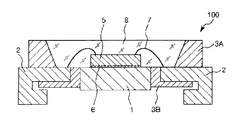
- 1 is a longitudinal sectional view showing a first embodiment of an optical semiconductor device.
- It is a longitudinal cross-sectional view which shows 2nd Embodiment of an optical semiconductor device.
- FIG. 1 is a longitudinal sectional view showing a first embodiment of the substrate for mounting an optical semiconductor element
- FIG. 2 is a longitudinal sectional view showing the first embodiment of the optical semiconductor device.
- an optical semiconductor element mounting substrate 10 As shown in FIG. 1, an optical semiconductor element mounting substrate 10 according to this embodiment includes a mounting portion 1 on which an optical semiconductor element 5 is to be mounted, a wiring pattern 2 disposed adjacent to the mounting portion 1, and a mounting.
- the reflection member 3 ⁇ / b> A is formed so as to surround the portion 1, and the reflection member 3 ⁇ / b> B is provided between the mounting portion 1 and the wiring pattern 2.
- the mounting portion 1 is a portion on which an optical semiconductor element 5 described later is mounted, and is located at substantially the center of the optical semiconductor element mounting substrate 10.
- the mounting portion 1 is made of a conductive material and is configured to be electrically connected to the optical semiconductor element 5.
- the wiring pattern 2 is arranged around the mounting portion 1 and is made of a conductive material like the mounting portion 1.
- the wiring pattern 2 is configured to be electrically connected to the optical semiconductor element 5 by a bonding wire 7 described later.
- the reflecting member 3A and the reflecting member 3B are made of the resin composition for light reflection of the present invention described later.
- the reflecting member 3 ⁇ / b> A and the reflecting member 3 ⁇ / b> B have a function of reflecting light emitted from the optical semiconductor element 5.
- the reflective member 3A is formed so as to surround the mounting portion 1 (optical semiconductor element 5).
- the reflection member 3 ⁇ / b> A has a surface on the mounting portion 1 side that is inclined outward.
- the reflective member 3B is formed so as to fill the space between the mounting portion 1 and the wiring pattern 2, and is formed integrally with the reflective member 3A.
- the optical semiconductor device 100 includes the above-described optical semiconductor element mounting substrate 10 and the optical semiconductor element 5 mounted on the mounting portion 1 of the optical semiconductor element mounting substrate 10. .
- the optical semiconductor element 5 is mounted on the mounting portion 1 of the optical semiconductor element mounting substrate 10 by a die attach material 6 (die attach paste, die attach film, etc.).
- a die attach material 6 die attach paste, die attach film, etc.
- the optical semiconductor element 5 is electrically connected to the wiring pattern 2 by bonding wires 7.
- optical semiconductor element 5 and the bonding wire 7 are sealed with a transparent sealing material 8 as shown in FIG.
- optical semiconductor element 5 examples include a light emitting element such as an LED (Light Emitting Diode), a liquid crystal display element, a semiconductor laser element using a compound semiconductor, and a light receiving element such as a photocoupler.
- a light emitting element such as an LED (Light Emitting Diode)
- a liquid crystal display element such as a liquid crystal display element
- a semiconductor laser element using a compound semiconductor such as a light receiving element
- a photocoupler such as a photocoupler
- the resin composition for light reflection of the present invention is a material used to form a reflection member as described above, and an epoxy having a unit structure X of alicyclic acid anhydride and a unit structure Y of hydrogenated bisphenol. Resin B and a colorant are included.
- the epoxy resin B preferably further has a unit structure Z of bisphenol type epoxy.
- the resin composition for light reflections of this invention further contains the epoxy resin A which has a structure represented by following formula (1).
- the light reflecting resin composition of the present invention further includes an epoxy resin C having an isocyanuric ring.
- the conventional light-reflecting resin composition has low moldability and is difficult to mold into a desired shape.
- the conventional light reflecting resin composition has low heat resistance, and yellowing occurs due to heat during molding, heat during soldering, heat of the light emitting element, and the like, resulting in a decrease in reflectance. It was. Moreover, there also existed a problem that peeling and a crack produced in a light reflection member with heat.
- the epoxy resin B having the above structure by including the epoxy resin B having the above structure and a colorant, characteristics such as reflectance are deteriorated due to yellowing caused by heat during molding, heat from the light emitting element, or the like. Can be prevented. Further, it is possible to prevent the reflective member from being peeled off or cracked by heat. That is, it is possible to provide a light reflecting resin composition having excellent heat resistance.
- the moldability of the light reflecting resin composition can be improved.
- the resin composition for light reflection further contains the epoxy resin C, the light resistance of the resin composition for light reflection can be improved.
- Epoxy resin A has a structure represented by the above formula (1). By including such an epoxy resin A, the moldability of the light reflecting resin composition can be improved.
- R is a monovalent organic group having 2 to 10 carbon atoms, and specifically, a group derived from 2,2-bis (hydroxyethyl) -1-butanol. Is preferred.
- the weight average molecular weight of such an epoxy resin A is preferably 500 to 5000, and more preferably 1000 to 3000. Thereby, a moldability can be improved more effectively, maintaining the outstanding heat resistance.
- the content of epoxy resin A in the light reflecting resin composition is preferably 1 to 15% by mass, more preferably 5 to 10% by mass. Thereby, moldability can be improved more efficiently, suppressing yellowing by heat.
- Epoxy resin B has a unit structure X of alicyclic acid anhydride and a unit structure Y of hydrogenated bisphenol.
- the epoxy resin B preferably further has a unit structure Z of bisphenol type epoxy.
- Examples of the unit structure X of the alicyclic acid anhydride include acid anhydride structures such as hexahydrophthalic acid and tetrahydrophthalic acid. Among these, it is preferable to have a unit structure of an acid anhydride of hexahydrophthalic acid. Thereby, moldability can be further improved while improving heat resistance.
- the content of the unit structure X of the alicyclic acid anhydride contained in the epoxy resin B is x [mass%] and the content of the unit structure Y of the hydrogenated bisphenol is y [mass%], 0.5 It is preferable that the relationship of ⁇ y / x is satisfied. By satisfying such a relationship, yellowing due to heat at the time of molding, heat at the time of soldering, heat of the light emitting element, or the like can be more reliably prevented. Further, it is possible to more effectively prevent the reflective member from being cracked or peeled off due to heat at the time of molding, heat at the time of soldering, heat of the light emitting element, or the like.
- the content of the unit structure X of the alicyclic acid anhydride contained in the epoxy resin B is x [mass%] and the content of the unit structure Z of the bisphenol type epoxy is z [mass%], 1 It is preferable to satisfy the relationship of 0.0 ⁇ z / x. By satisfying such a relationship, yellowing due to heat during molding, heat from the light emitting element, or the like can be more reliably prevented.
- the content of the epoxy resin B in the light reflecting resin composition is preferably 1 to 15% by mass, and more preferably 1 to 10% by mass.
- the content of the epoxy resin A is M [mass%] and the content of the epoxy resin B is N [mass%], it is preferable that the relationship of 0.1 ⁇ M / N ⁇ 10 is satisfied. More preferably, the relationship of 5 ⁇ M / N ⁇ 6.0 is satisfied. By satisfying such a relationship, moldability and heat resistance can be improved more efficiently.
- Epoxy resin C is an epoxy resin having an isocyanuric ring.
- the epoxy resin C is not particularly limited as long as it has two or more epoxy groups and an isocyanuric ring in the molecule.
- an epoxy resin having a structure in which two or more glycidyl groups are bonded to a nitrogen atom of one isocyanuric ring can be mentioned.
- the light resistance of the light reflecting resin composition can be improved.
- the weight average molecular weight of the epoxy resin C is preferably 200 to 3000, and more preferably 240 to 1500. Thereby, light resistance can be improved more effectively, maintaining the outstanding heat resistance.
- the content of the epoxy resin C in the light reflecting resin composition is preferably 1 to 15% by mass, and more preferably 5 to 10% by mass. Thereby, light resistance can be improved more efficiently, suppressing yellowing by heat.
- the light reflecting resin composition of the present invention preferably contains a curing agent.
- the curing agent is not particularly limited, and those generally used as a curing agent for epoxy resins can be used.
- a curing agent include an acid anhydride curing agent, an isocyanuric acid derivative curing agent, and a phenol curing agent.
- the acid anhydride curing agent include phthalic anhydride, maleic anhydride, trimellitic anhydride, pyromellitic anhydride, hexahydrophthalic anhydride, tetrahydrophthalic anhydride, methyl nadic anhydride, nadic anhydride, glutaric anhydride.
- Isocyanuric acid derivatives include 1,3,5-tris (1-carboxymethyl) isocyanurate, 1,3,5-tris (2-carboxyethyl) isocyanurate, 1,3,5-tris (3-carboxypropyl) ) Isocyanurate, 1,3-bis (2-carboxyethyl) isocyanurate.
- tetrahydrophthalic anhydride is preferably used, and 1,2,3,6-tetrahydrophthalic anhydride is more preferably used. Thereby, a moldability and heat resistance can further be improved.
- the curing agent has 0.5 to 1.0 equivalent of an active group (an acid anhydride group or a hydroxyl group) in the curing agent capable of reacting with the epoxy group with respect to 1 equivalent of the epoxy group in the epoxy resin. It is preferable to blend them in such a manner that 0.6 to 0.9 equivalents are more preferable. Thereby, hardening of the resin composition for light reflection can be advanced more reliably. Further, the heat resistance of the reflecting member can be made higher.
- an active group an acid anhydride group or a hydroxyl group
- the resin composition for light reflection contains a colorant.
- the colorant it is preferable to use a colorant having high light reflectivity, and it is particularly preferable to use a white pigment.
- white pigment known pigments can be used and are not particularly limited.
- white pigments include alumina, magnesium oxide, antimony oxide, titanium oxide, zirconium oxide, and inorganic hollow particles. Among these, one or more of these can be used in combination. Among these, when titanium oxide is used, the light reflectance can be further increased. In addition, such a white pigment functions also as an inorganic filler mentioned later.
- the content of the colorant is preferably 50% by mass or less, and more preferably 10 to 40% by mass. Thereby, light reflectance can be improved more, maintaining the intensity
- the light reflecting resin composition may contain, for example, an inorganic filler, a curing accelerator, a coupling agent, and the like.
- the light reflecting resin composition may contain an inorganic filler.
- inorganic fillers examples include silica, antimony oxide, aluminum hydroxide, magnesium hydroxide, barium sulfate, magnesium carbonate, barium carbonate, alumina, mica, beryllia, barium titanate, potassium titanate, strontium titanate, calcium titanate , Aluminum carbonate, aluminum silicate, calcium carbonate, calcium silicate, magnesium silicate, silicon nitride, boron nitride, clay such as calcined clay, talc, aluminum borate, and silicon carbide.
- silica as the inorganic filler. Thereby, the heat resistance of a reflective member can be improved more.
- the average particle diameter of the inorganic filler is preferably 5 to 30 ⁇ m, and more preferably 10 to 25 ⁇ m.
- the content of the inorganic filler in the light reflecting resin composition is preferably 30% by mass or more, and more preferably 40 to 80% by mass. Thereby, heat resistance can further be improved, maintaining the excellent moldability.
- the resin composition for light reflection may contain a curing accelerator.
- curing accelerator examples include amine compounds, imidazole compounds, organic phosphorus compounds, alkali metal compounds, alkaline earth metal compounds, quaternary ammonium salts, and the like, and these may be used alone or in combination of two or more. it can.
- an amine compound an imidazole compound, or an organic phosphorus compound.
- the amine compound include 1,8-diaza-bicyclo (5.4.0) undecene-7, triethylenediamine, and tri-2,4,6-dimethylaminomethylphenol.
- the imidazole compound include 2-ethyl-4-methylimidazole.
- organic phosphorus compound for example, triphenylphosphine, tetraphenylphosphonium tetraphenylborate, tetra-n-butylphosphonium-o, o-diethylphosphorodithioate, tetra-n-butylphosphonium-tetrafluoroborate, tetra -N-butylphosphonium-tetraphenylborate.
- the content of the curing accelerator in the resin composition for light reflection is preferably 0.05 to 5.0% by mass, and more preferably 0.1 to 1.0% by mass.
- the resin composition for light reflection may contain the coupling agent. Thereby, the adhesiveness of the said epoxy resin, a coloring agent, etc. can be improved.
- the coupling agent is not particularly limited, and examples thereof include a silane coupling agent and a titanate coupling agent.
- silane coupling agents generally include epoxy silanes, amino silanes, cationic silanes, vinyl silanes, acrylic silanes, mercapto silanes, and composites thereof, which can be used in any amount.
- the content of the coupling agent in the light reflecting resin composition is preferably 5% by mass or less.
- the light reflecting resin composition of the present invention may contain additives such as an antioxidant, a release agent, and an ion scavenger in addition to the above components.
- the iron ion concentration is preferably 15 ppm or less, and more preferably 10 ppm or less. Thereby, the light reflectance can be further improved.
- the measuring method of iron ion concentration can be measured by atomic absorption spectrometry.
- Such a light reflecting resin composition can be obtained by uniformly dispersing and mixing the various components described above.
- the above components are kneaded by an extruder, a kneader, a roll, an extruder, etc., and then the kneaded product is cooled and pulverized.
- the light reflecting resin composition thus obtained can be molded by a method such as injection molding, transfer molding or compression molding to obtain a reflecting member.
- FIG. 3 is a longitudinal sectional view showing a second embodiment of the optical semiconductor device.
- the optical semiconductor device 100 ′ includes a mounting portion 1 on which the optical semiconductor element 5 is mounted, a wiring pattern 2 disposed adjacent to the mounting portion 1, and the mounting portion 1.
- a reflection member 3 and an optical semiconductor element 5 are disposed around the periphery.
- optical semiconductor element 5 is mounted on the mounting portion 1 by the die attach material 6 in the same manner as the above-described embodiment.
- the optical semiconductor element 5 is electrically connected to the wiring pattern 2 by bonding wires 7.
- the optical semiconductor element 5 and the bonding wire 7 are sealed with a transparent sealing material 8 as shown in FIG.
- optical semiconductor element 5 examples include a light emitting element such as an LED (Light Emitting Diode), a liquid crystal display element, a semiconductor laser element using a compound semiconductor, and a light receiving element such as a photocoupler.
- a light emitting element such as an LED (Light Emitting Diode)
- a liquid crystal display element such as a liquid crystal display element
- a semiconductor laser element using a compound semiconductor such as a light receiving element
- a photocoupler such as a photocoupler
- the optical semiconductor device 100 ′ of this embodiment is different from the above-described embodiment in that the reflecting member 3 having no inclined surface is used.
- the light reflecting resin composition, the optical semiconductor element mounting substrate, and the optical semiconductor device of the present invention have been described above.
- the present invention is not limited to this, and for example, the optical semiconductor element mounting substrate and the optical semiconductor Arbitrary components may be added to the apparatus.
- the resin composition for light reflection was obtained by melt-kneading using a kneader, followed by cooling and pulverization.
- the silica was a particle cut of 30 ⁇ m or more.
- EHPE-3150 (manufactured by Daicel Chemical Industries) is a 1,2-epoxy-4- (2-oxiranyl) cyclohexane adduct of 2,2-bis (hydroxymethyl) -1-butanol.
- ST-6100 (manufactured by Nippon Steel Chemical Co., Ltd., softening point 100 ° C.) is a polymerization of hexahydrophthalic acid anhydride, 2,2′-bis (4-hydroxycyclohexyl) propane and bisphenol A type epoxy. It is a reaction product.
- TEPIC-SP (manufactured by Nissan Chemical Co., Ltd.) is triglycidyl isocyanurate.
- MA-DGIC (manufactured by Shikoku Chemicals) is monoallyl diglycidyl isocyanurate.
- each example and each comparative example was 15 ppm or less as measured by atomic absorption spectrometry.
- the composition of each example and each comparative example is shown in Table 1.
- the quality of the whiteness was judged as follows. ⁇ : Whiteness is 90% or more ⁇ : Whiteness is 80% or more and less than 90% ⁇ : Whiteness is 70% or more and less than 80% ⁇ : Whiteness is less than 70%
- A Good filling property and releasability, no problem.
- ⁇ The mold was released by air.
- ⁇ It was difficult to release even if air was applied.
- X Unfilled resin composition for light reflection is seen and molding is poor.
- the light reflecting resin composition of the present invention was excellent in moldability. Moreover, in the optical semiconductor element mounting substrate using the light reflecting resin composition of the present invention, the heat resistance was excellent and the decrease in the light reflectance was suppressed. On the other hand, satisfactory results were not obtained in the comparative example.
Landscapes
- Chemical & Material Sciences (AREA)
- Health & Medical Sciences (AREA)
- Chemical Kinetics & Catalysis (AREA)
- Medicinal Chemistry (AREA)
- Polymers & Plastics (AREA)
- Organic Chemistry (AREA)
- Led Device Packages (AREA)
- Compositions Of Macromolecular Compounds (AREA)
- Epoxy Resins (AREA)
Abstract
Description
(1) 脂環式酸無水物の単位構造Xと水素化ビスフェノールの単位構造Yとを有するエポキシ樹脂Bと、
着色剤と、
を含むことを特徴とする光反射用樹脂組成物。
(2) 上記エポキシ樹脂Bは、さらにビスフェノール型エポキシの単位構造Zを有する、(1)に記載の光反射用樹脂組成物。
(3) 下記式(1)で表される構造を有するエポキシ樹脂Aをさらに含む、(1)または(2)に記載の光反射用樹脂組成物。

(5) 上記エポキシ樹脂Aの含有量は、1~15質量%である(3)または(4)に記載の光反射用樹脂組成物。
(6) 上記エポキシ樹脂Bの含有量は、1~15質量%である(1)ないし(5)のいずれか1つに記載の光反射用樹脂組成物。
(7) イソシアヌル環を有するエポキシ樹脂Cをさらに含む、(1)ないし(6)のいずれか1つに記載の光反射用樹脂組成物。
(8) 上記エポキシ樹脂Cの含有量は、1~15質量%である(7)に記載の光反射用樹脂組成物。
(9) さらに硬化剤を含む、(1)ないし(8)のいずれか1つに記載の光反射用樹脂組成物。
(10) 鉄イオンの濃度が、15ppm以下である(1)ないし(9)のいずれか1つに記載の光反射用樹脂組成物。
(11) 無機充填材を含み、
当該無機充填材の含有量は、30質量%以上である(1)ないし(10)のいずれか1つに記載の光反射用樹脂組成物。
(12) 上記着色剤は、酸化チタンである(1)ないし(11)のいずれか1つに記載の光反射用樹脂組成物。
(13) 上記着色剤の含有量は、50質量%以下である(1)ないし(12)のいずれか1つに記載の光反射用樹脂組成物。
(14) (1)ないし(13)のいずれか1つに記載の光反射用樹脂組成物で構成された反射部材を備えたことを特徴とする光半導体素子搭載用基板。
(15) (1)ないし(13)のいずれか1つに記載の光反射用樹脂組成物で構成された反射部材と、発光素子と、を備えることを特徴とする光半導体装置。
まず、本発明の光反射用樹脂組成物の説明に先立ち、光半導体素子搭載用基板および光半導体装置の第1実施形態について説明する。
図1に示すように、本実施形態に係る光半導体素子搭載用基板10は、光半導体素子5を搭載すべき搭載部1と、搭載部1に隣接して配された配線パターン2と、搭載部1を囲むように形成された反射部材3Aと、搭載部1と配線パターン2との間に設けられた反射部材3Bとを有している。
光半導体装置100は、図2に示すように、上述した光半導体素子搭載用基板10と、当該光半導体素子搭載用基板10の搭載部1に搭載された光半導体素子5とを有している。
次に、本発明の光反射用樹脂組成物について説明する。
また、本発明の光反射用樹脂組成物は、下記式(1)で表される構造を有するエポキシ樹脂Aをさらに含むことが好ましい。

[エポキシ樹脂A]
エポキシ樹脂Aは、上記式(1)で表される構造を有している。このようなエポキシ樹脂Aを含むことにより、光反射用樹脂組成物の成形性を向上させることができる。
エポキシ樹脂Bは、脂環式酸無水物の単位構造Xと、水素化ビスフェノールの単位構造Yとを有している。また、エポキシ樹脂Bは、さらにビスフェノール型エポキシの単位構造Zを有することが好ましい。このようなエポキシ樹脂Bを含むことにより、光反射用樹脂組成物の耐熱性を向上させることができる。
エポキシ樹脂Cは、イソシアヌル環を有するエポキシ樹脂である。エポキシ樹脂Cは分子中に2以上のエポキシ基とイソシアヌル環を有するものであれば特に限定されない。例えば、2つ以上のグリシジル基が1つのイソシアヌル環の窒素原子に結合した構造を有するエポキシ樹脂が挙げられる。
このようなエポキシ樹脂Cを含むことにより、光反射用樹脂組成物の耐光性を向上させることができる。
本発明の光反射用樹脂組成物は、硬化剤を含んでいるのが好ましい。
光反射用樹脂組成物は、着色剤を含んでいる。
光反射用樹脂組成物は、上記成分の他、例えば、無機充填材、硬化促進剤、カップリング剤等を含んでいてもよい。
光反射用樹脂組成物は、無機充填材を含んでいてもよい。
光反射用樹脂組成物は、硬化促進剤を含んでいてもよい。
また、光反射用樹脂組成物は、カップリング剤を含んでいてもよい。これにより、上記エポキシ樹脂と、着色剤等との接着性を向上させることができる。
なお、鉄イオン濃度の測定方法は、原子吸光分析法により測定することができる。
次に、光半導体装置の第2実施形態について説明する。
図3は、光半導体装置の第2実施形態を示す縦断面図である。
[1]光反射用樹脂組成物の製造
(実施例1~13)
表1に示す各成分を、ミキサーを用いて10~50℃で均一に混合した。
エポキシ樹脂Bを添加せず、上記実施例と同様の方法により、光反射用樹脂組成物を得た。
エポキシ樹脂Aおよびエポキシ樹脂Bを添加せず、上記実施例と同様の方法により、光反射用樹脂組成物を得た。
また、EHPE-3150(ダイセル化学工業社製)は、2,2-ビス(ヒドロキシメチル)-1-ブタノールの1,2-エポキシ-4-(2-オキシラニル)シクロヘキサン付加物である。
また、ST-6100(新日鐵化学社製、軟化点100℃)は、ヘキサヒドロフタル酸の酸無水物と2,2'-ビス(4-ヒドロキシシクロヘキシル)プロパンとビスフェノールA型エポキシとの重合反応生成物である。
また、TEPIC-SP(日産化学社製)は、トリグリシジルイソシアヌレートである。また、MA-DGIC(四国化成工業社製)は、モノアリルジグリシジルイソシアヌレートである。
各実施例および各比較例の組成を表1に示した。

得られた光反射用樹脂組成物を銀メッキされた銅フレーム上に、成形温度:175℃、注入圧力:12MPa、硬化時間:120秒の条件で反射部材を形成した。
[3-1]光反射率(白色度)の評価
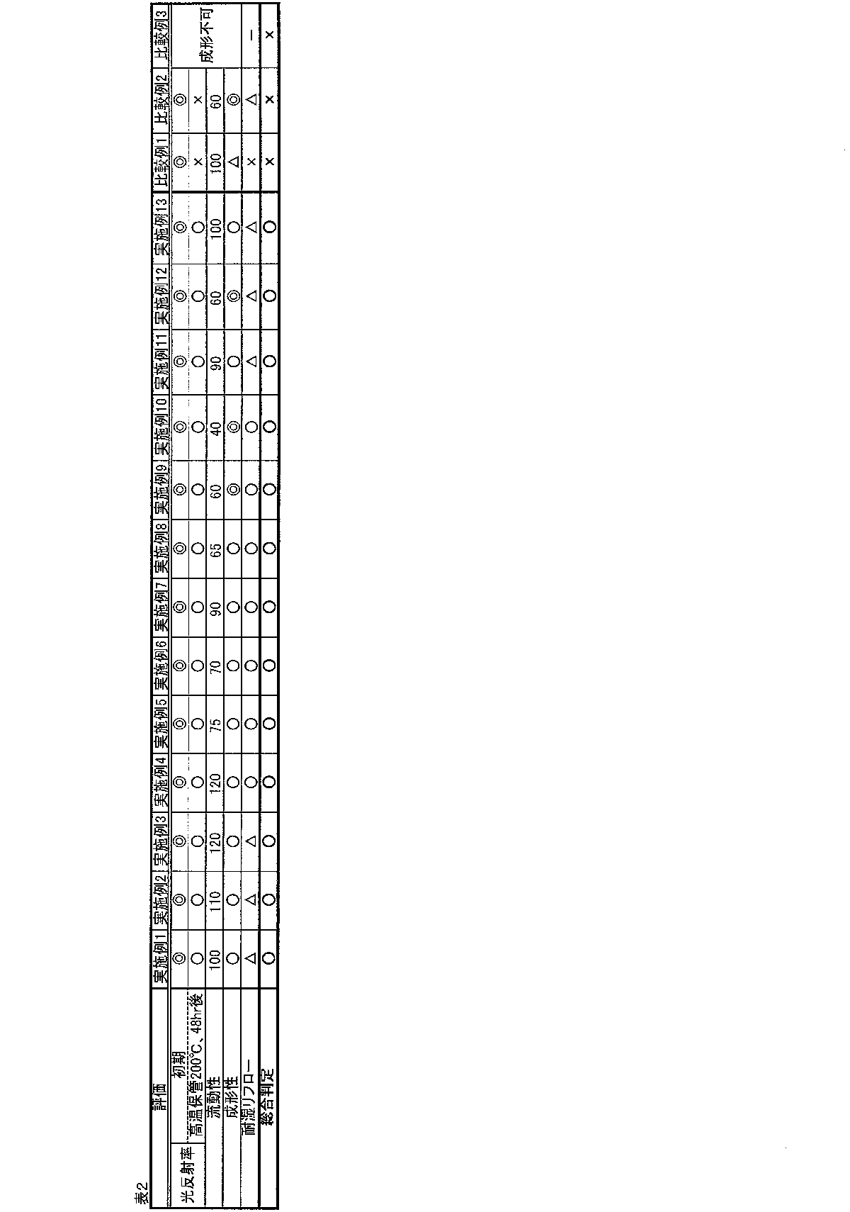
得られた光反射用樹脂組成物を低圧トランスファー成形機(藤和精機社製、TEP-50-30)を用いて、金型温度175℃、注入圧力9.8MPa、硬化時間120秒間の条件下で成形し、直径50mmΦ、厚さ2.5mmの試験円盤を作製した。色彩計(カラーリーダー、CR13、コニカミノルタ製)を用いて、上記試験円盤の表面の初期白色度と200℃、48時間処理後の白色度を測定した。
◎ :白色度が90%以上
○ :白色度が80%以上、90%未満
△ :白色度が70%以上、80%未満
× :白色度が70%未満
スパイラルフロー:低圧トランスファー成形機(コータキ精機株式会社製、KTS-15)を用いて、EMMI-1-66に準じたスパイラルフロー測定用金型に、175℃、注入圧力6.9MPa、保圧時間120秒間の条件で光反射用樹脂組成物を注入し、流動長(cm)を測定した。
得られた光反射用樹脂組成物をトランスファー成形機(藤和精機(株)製、TEP-50-30)を用いて、金型温度175℃、注入圧力9.8MPa、硬化時間120秒間の条件下で成形し、直径50mmΦ、厚さ2.5mmの試験円盤を作成した。この試験円盤を成形金型から取り外す際の離型し易さおよび外観の状態を以下のように評価した。
○ :エアー掛けして離型できた。
△ :エアー掛けしても離型し難かった。
× :光反射用樹脂組成物の未充填が見られ、成形不良。
上記[2]の方法により、作製した光半導体素子搭載用基板をポストキュアとして150℃で4時間加熱処理し、その後、30℃、相対湿度60%で168時間加湿処理した。その後、IRリフロー処理(260℃、JEDEC・LEVEL3)を行い、光反射用樹脂組成物(成形品)と光半導体素子搭載用基板との界面の密着状態、及びクラックの有無を超音波探傷機(日立建機ファインテック製)で観察した。剥離発生率[剥離発生素子数/全光半導体素子数×100(%)]を算出し、以下の判断基準で評価した。
○ :剥離発生無し
△ :剥離発生率が20%未満
× :剥離発生率が20%以上
評価結果を表2に示した。
Claims (15)
- 脂環式酸無水物の単位構造Xと水素化ビスフェノールの単位構造Yとを有するエポキシ樹脂Bと、
着色剤と、
を含むことを特徴とする光反射用樹脂組成物。 - 前記エポキシ樹脂Bは、さらにビスフェノール型エポキシの単位構造Zを有する、請求項1に記載の光反射用樹脂組成物。
- 下記式(1)で表される構造を有するエポキシ樹脂Aをさらに含む、請求項1または2に記載の光反射用樹脂組成物。

- 前記エポキシ樹脂Aの含有量をM[質量%]、前記エポキシ樹脂Bの含有量をN[質量%]としたとき、0.1≦M/N≦10の関係を満足する請求項3に記載の光反射用樹脂組成物。
- 前記エポキシ樹脂Aの含有量は、1~15質量%である請求項3または4に記載の光反射用樹脂組成物。
- 前記エポキシ樹脂Bの含有量は、1~15質量%である請求項1ないし5のいずれか1項に記載の光反射用樹脂組成物。
- イソシアヌル環を有するエポキシ樹脂Cをさらに含む、請求項1ないし6のいずれか1項に記載の光反射用樹脂組成物。
- 前記エポキシ樹脂Cの含有量は、1~15質量%である請求項7に記載の光反射用樹脂組成物。
- さらに硬化剤を含む、請求項1ないし8のいずれか1項に記載の光反射用樹脂組成物。
- 鉄イオンの濃度が、15ppm以下である請求項1ないし9のいずれか1項に記載の光反射用樹脂組成物。
- 無機充填材を含み、
当該無機充填材の含有量は、30質量%以上である請求項1ないし10のいずれか1項に記載の光反射用樹脂組成物。 - 前記着色剤は、酸化チタンである請求項1ないし11のいずれか1項に記載の光反射用樹脂組成物。
- 前記着色剤の含有量は、50質量%以下である請求項1ないし12のいずれか1項に記載の光反射用樹脂組成物。
- 請求項1ないし13のいずれか1項に記載の光反射用樹脂組成物で構成された反射部材を備えたことを特徴とする光半導体素子搭載用基板。
- 請求項1ないし13のいずれか1項に記載の光反射用樹脂組成物で構成された反射部材と、発光素子と、を備えることを特徴とする光半導体装置。
Priority Applications (4)
| Application Number | Priority Date | Filing Date | Title |
|---|---|---|---|
| KR1020147028840A KR20140148417A (ko) | 2012-03-27 | 2013-03-14 | 광 반사용 수지 조성물, 광 반도체 소자 탑재용 기판 및 광 반도체 장치 |
| SG11201404289WA SG11201404289WA (en) | 2012-03-27 | 2013-03-14 | Resin composition for reflecting light, substrate for mounting optical semiconductor element, and optical semiconductor device |
| CN201380016746.5A CN104204024A (zh) | 2012-03-27 | 2013-03-14 | 光反射用树脂组合物、光半导体元件搭载用基板和光半导体装置 |
| US14/376,032 US20150014729A1 (en) | 2012-03-27 | 2013-03-14 | Resin composition for reflecting light, substrate for mounting optical semiconductor element, and optical semiconductor device |
Applications Claiming Priority (6)
| Application Number | Priority Date | Filing Date | Title |
|---|---|---|---|
| JP2012-072566 | 2012-03-27 | ||
| JP2012072566 | 2012-03-27 | ||
| JP2012-112746 | 2012-05-16 | ||
| JP2012112746 | 2012-05-16 | ||
| JP2012-148620 | 2012-07-02 | ||
| JP2012148620 | 2012-07-02 |
Publications (1)
| Publication Number | Publication Date |
|---|---|
| WO2013145607A1 true WO2013145607A1 (ja) | 2013-10-03 |
Family
ID=49258922
Family Applications (1)
| Application Number | Title | Priority Date | Filing Date |
|---|---|---|---|
| PCT/JP2013/001693 Ceased WO2013145607A1 (ja) | 2012-03-27 | 2013-03-14 | 光反射用樹脂組成物、光半導体素子搭載用基板および光半導体装置 |
Country Status (7)
| Country | Link |
|---|---|
| US (1) | US20150014729A1 (ja) |
| JP (1) | JPWO2013145607A1 (ja) |
| KR (1) | KR20140148417A (ja) |
| CN (1) | CN104204024A (ja) |
| SG (1) | SG11201404289WA (ja) |
| TW (1) | TW201348326A (ja) |
| WO (1) | WO2013145607A1 (ja) |
Cited By (3)
| Publication number | Priority date | Publication date | Assignee | Title |
|---|---|---|---|---|
| WO2016017531A1 (ja) * | 2014-07-31 | 2016-02-04 | 株式会社ダイセル | 硬化性樹脂組成物及びその硬化物、光半導体素子搭載用基板、並びに光半導体装置 |
| JP2016046398A (ja) * | 2014-08-25 | 2016-04-04 | 株式会社カネカ | 光半導体パッケージ集合体、発光装置 |
| JP2018009065A (ja) * | 2016-07-11 | 2018-01-18 | パナソニックIpマネジメント株式会社 | エポキシ樹脂組成物、プリプレグ、金属張積層板及びプリント配線板 |
Families Citing this family (1)
| Publication number | Priority date | Publication date | Assignee | Title |
|---|---|---|---|---|
| US12537328B2 (en) | 2023-04-24 | 2026-01-27 | Google Llc | Force distributing spring contacts |
Citations (5)
| Publication number | Priority date | Publication date | Assignee | Title |
|---|---|---|---|---|
| JP2002317178A (ja) * | 1996-09-20 | 2002-10-31 | Siemens Ag | 波長変換注型材料及びその製造方法並びに発光素子 |
| JP2006241353A (ja) * | 2005-03-04 | 2006-09-14 | Kyocera Chemical Corp | エポキシ樹脂組成物及び電子部品装置 |
| JP2008106180A (ja) * | 2006-10-26 | 2008-05-08 | Matsushita Electric Works Ltd | 光半導体封止用樹脂組成物及び光半導体装置 |
| JP2010120989A (ja) * | 2008-11-17 | 2010-06-03 | Toto Kasei Co Ltd | エポキシ樹脂組成物 |
| JP2011122116A (ja) * | 2009-12-14 | 2011-06-23 | Hitachi Chem Co Ltd | 熱硬化性樹脂組成物、光半導体素子搭載用基板及びその製造方法、並びに光半導体装置 |
Family Cites Families (3)
| Publication number | Priority date | Publication date | Assignee | Title |
|---|---|---|---|---|
| EP1441395B9 (de) * | 1996-06-26 | 2012-08-15 | OSRAM Opto Semiconductors GmbH | Lichtabstrahlendes Halbleiterbauelement mit Lumineszenzkonversionselement |
| JP2011074355A (ja) * | 2009-09-07 | 2011-04-14 | Nitto Denko Corp | 光半導体装置用樹脂組成物およびそれを用いて得られる光半導体装置用リードフレーム、ならびに光半導体装置 |
| CN103080144B (zh) * | 2010-05-28 | 2015-02-25 | 住友电木株式会社 | 酯化物的制造方法 |
-
2013
- 2013-03-14 SG SG11201404289WA patent/SG11201404289WA/en unknown
- 2013-03-14 CN CN201380016746.5A patent/CN104204024A/zh active Pending
- 2013-03-14 KR KR1020147028840A patent/KR20140148417A/ko not_active Withdrawn
- 2013-03-14 US US14/376,032 patent/US20150014729A1/en not_active Abandoned
- 2013-03-14 WO PCT/JP2013/001693 patent/WO2013145607A1/ja not_active Ceased
- 2013-03-14 JP JP2014507385A patent/JPWO2013145607A1/ja active Pending
- 2013-03-15 TW TW102109346A patent/TW201348326A/zh unknown
Patent Citations (5)
| Publication number | Priority date | Publication date | Assignee | Title |
|---|---|---|---|---|
| JP2002317178A (ja) * | 1996-09-20 | 2002-10-31 | Siemens Ag | 波長変換注型材料及びその製造方法並びに発光素子 |
| JP2006241353A (ja) * | 2005-03-04 | 2006-09-14 | Kyocera Chemical Corp | エポキシ樹脂組成物及び電子部品装置 |
| JP2008106180A (ja) * | 2006-10-26 | 2008-05-08 | Matsushita Electric Works Ltd | 光半導体封止用樹脂組成物及び光半導体装置 |
| JP2010120989A (ja) * | 2008-11-17 | 2010-06-03 | Toto Kasei Co Ltd | エポキシ樹脂組成物 |
| JP2011122116A (ja) * | 2009-12-14 | 2011-06-23 | Hitachi Chem Co Ltd | 熱硬化性樹脂組成物、光半導体素子搭載用基板及びその製造方法、並びに光半導体装置 |
Cited By (3)
| Publication number | Priority date | Publication date | Assignee | Title |
|---|---|---|---|---|
| WO2016017531A1 (ja) * | 2014-07-31 | 2016-02-04 | 株式会社ダイセル | 硬化性樹脂組成物及びその硬化物、光半導体素子搭載用基板、並びに光半導体装置 |
| JP2016046398A (ja) * | 2014-08-25 | 2016-04-04 | 株式会社カネカ | 光半導体パッケージ集合体、発光装置 |
| JP2018009065A (ja) * | 2016-07-11 | 2018-01-18 | パナソニックIpマネジメント株式会社 | エポキシ樹脂組成物、プリプレグ、金属張積層板及びプリント配線板 |
Also Published As
| Publication number | Publication date |
|---|---|
| TW201348326A (zh) | 2013-12-01 |
| JPWO2013145607A1 (ja) | 2015-12-10 |
| US20150014729A1 (en) | 2015-01-15 |
| SG11201404289WA (en) | 2014-10-30 |
| CN104204024A (zh) | 2014-12-10 |
| KR20140148417A (ko) | 2014-12-31 |
Similar Documents
| Publication | Publication Date | Title |
|---|---|---|
| JP5298468B2 (ja) | 熱硬化性光反射用樹脂組成物、これを用いた光半導体素子搭載用基板とその製造方法および光半導体装置 | |
| JP6361761B2 (ja) | 発光装置及びその製造方法並びに成形体 | |
| JP5764423B2 (ja) | 光半導体装置用エポキシ樹脂組成物およびそれを用いて得られる光半導体装置用リードフレームまたは光半導体装置用基板、ならびに光半導体装置 | |
| JP5599561B2 (ja) | 熱硬化性樹脂組成物、これを用いた光半導体素子搭載用基板及びその製造方法並びに光半導体装置 | |
| JP5119368B1 (ja) | 光半導体装置用白色硬化性組成物の製造方法及び光半導体装置用成形体の製造方法 | |
| JP6096090B2 (ja) | 熱硬化性樹脂組成物、これを用いた光半導体素子搭載用基板及びその製造方法並びに光半導体装置 | |
| JP5233186B2 (ja) | 熱硬化性光反射用樹脂組成物、これを用いた光半導体素子搭載用基板とその製造方法および光半導体装置 | |
| JP6061471B2 (ja) | 光半導体装置及び光半導体装置の製造方法 | |
| JPWO2013145607A1 (ja) | 光反射用樹脂組成物、光半導体素子搭載用基板および光半導体装置 | |
| JP6133004B2 (ja) | 光反射用熱硬化性樹脂組成物、光半導体素子搭載用基板及びその製造方法、並びに光半導体装置 | |
| JP2009246334A (ja) | 光反射用熱硬化性樹脂組成物、光半導体素子搭載用基板及びその製造方法、並びに光半導体装置 | |
| JP2011122116A (ja) | 熱硬化性樹脂組成物、光半導体素子搭載用基板及びその製造方法、並びに光半導体装置 | |
| WO2013146404A1 (ja) | 光半導体装置用白色硬化性組成物、光半導体装置用成形体及び光半導体装置 | |
| TW202307059A (zh) | 光反射用熱硬化性樹脂組成物、光半導體元件搭載用基板及光半導體裝置 | |
| JP6191705B2 (ja) | 光反射用熱硬化性樹脂組成物、光半導体素子搭載用基板及びその製造方法、並びに光半導体装置 | |
| JP6883185B2 (ja) | 光半導体装置用熱硬化性樹脂組成物およびそれを用いて得られる光半導体装置用リードフレーム、光半導体装置、光半導体素子 | |
| JP5831424B2 (ja) | 光反射用熱硬化性樹脂組成物、光半導体素子搭載用基板及びその製造方法、並びに光半導体装置 | |
| KR101405532B1 (ko) | 에폭시 수지 조성물 및 이를 포함하는 광반도체 장치 | |
| CN114174372B (zh) | 光反射用热固性树脂组合物、光半导体元件搭载用基板及光半导体装置 | |
| JP7831992B2 (ja) | 光反射用熱硬化性樹脂組成物、光半導体素子搭載用基板及び光半導体装置 | |
| JP5798839B2 (ja) | 光半導体装置 | |
| JP6988234B2 (ja) | 光反射用熱硬化性樹脂組成物、光半導体素子搭載用基板及びその製造方法、並びに光半導体装置 | |
| JP5735378B2 (ja) | 光半導体装置用白色硬化性組成物、光半導体装置用成形体、光半導体装置用成形体の製造方法、光半導体装置及び光半導体装置の製造方法 | |
| JP6337996B2 (ja) | 光反射用熱硬化性樹脂組成物、光半導体素子搭載用基板及びその製造方法、並びに光半導体装置 | |
| JP2009298901A (ja) | 光半導体素子封止用固形エポキシ樹脂組成物およびそれを用いた光半導体装置 |
Legal Events
| Date | Code | Title | Description |
|---|---|---|---|
| 121 | Ep: the epo has been informed by wipo that ep was designated in this application |
Ref document number: 13768090 Country of ref document: EP Kind code of ref document: A1 |
|
| ENP | Entry into the national phase |
Ref document number: 2014507385 Country of ref document: JP Kind code of ref document: A |
|
| WWE | Wipo information: entry into national phase |
Ref document number: 14376032 Country of ref document: US |
|
| ENP | Entry into the national phase |
Ref document number: 20147028840 Country of ref document: KR Kind code of ref document: A |
|
| NENP | Non-entry into the national phase |
Ref country code: DE |
|
| 122 | Ep: pct application non-entry in european phase |
Ref document number: 13768090 Country of ref document: EP Kind code of ref document: A1 |