WO2013136895A1 - Semiconductor device - Google Patents
Semiconductor device Download PDFInfo
- Publication number
- WO2013136895A1 WO2013136895A1 PCT/JP2013/053292 JP2013053292W WO2013136895A1 WO 2013136895 A1 WO2013136895 A1 WO 2013136895A1 JP 2013053292 W JP2013053292 W JP 2013053292W WO 2013136895 A1 WO2013136895 A1 WO 2013136895A1
- Authority
- WO
- WIPO (PCT)
- Prior art keywords
- conductive
- block
- conductive pattern
- semiconductor device
- fixed
- Prior art date
Links
- 239000004065 semiconductor Substances 0.000 title claims abstract description 71
- 239000000758 substrate Substances 0.000 claims abstract description 68
- 239000011347 resin Substances 0.000 claims abstract description 35
- 229920005989 resin Polymers 0.000 claims abstract description 35
- 238000007789 sealing Methods 0.000 claims abstract description 19
- 230000003247 decreasing effect Effects 0.000 claims description 7
- 239000002184 metal Substances 0.000 claims description 7
- 229910052751 metal Inorganic materials 0.000 claims description 7
- 230000007423 decrease Effects 0.000 abstract description 4
- 229910052802 copper Inorganic materials 0.000 description 89
- 239000010949 copper Substances 0.000 description 89
- RYGMFSIKBFXOCR-UHFFFAOYSA-N Copper Chemical compound [Cu] RYGMFSIKBFXOCR-UHFFFAOYSA-N 0.000 description 87
- 238000005553 drilling Methods 0.000 description 18
- 230000000694 effects Effects 0.000 description 12
- 239000000919 ceramic Substances 0.000 description 11
- 239000000463 material Substances 0.000 description 6
- 230000035882 stress Effects 0.000 description 5
- 238000009792 diffusion process Methods 0.000 description 4
- 238000009413 insulation Methods 0.000 description 4
- 238000000034 method Methods 0.000 description 4
- 229910000679 solder Inorganic materials 0.000 description 4
- 230000008646 thermal stress Effects 0.000 description 4
- 125000004122 cyclic group Chemical group 0.000 description 3
- 230000002093 peripheral effect Effects 0.000 description 3
- 238000005336 cracking Methods 0.000 description 2
- 239000012528 membrane Substances 0.000 description 2
- 230000000149 penetrating effect Effects 0.000 description 2
- HBMJWWWQQXIZIP-UHFFFAOYSA-N silicon carbide Chemical compound [Si+]#[C-] HBMJWWWQQXIZIP-UHFFFAOYSA-N 0.000 description 2
- 229910010271 silicon carbide Inorganic materials 0.000 description 2
- 239000004020 conductor Substances 0.000 description 1
- 238000001816 cooling Methods 0.000 description 1
- 230000017525 heat dissipation Effects 0.000 description 1
- 230000002040 relaxant effect Effects 0.000 description 1
- 238000000926 separation method Methods 0.000 description 1
- 229910052710 silicon Inorganic materials 0.000 description 1
- 239000010703 silicon Substances 0.000 description 1
- 239000000126 substance Substances 0.000 description 1
Images


Classifications
-
- H—ELECTRICITY
- H05—ELECTRIC TECHNIQUES NOT OTHERWISE PROVIDED FOR
- H05K—PRINTED CIRCUITS; CASINGS OR CONSTRUCTIONAL DETAILS OF ELECTRIC APPARATUS; MANUFACTURE OF ASSEMBLAGES OF ELECTRICAL COMPONENTS
- H05K1/00—Printed circuits
- H05K1/02—Details
- H05K1/0296—Conductive pattern lay-out details not covered by sub groups H05K1/02 - H05K1/0295
-
- H—ELECTRICITY
- H01—ELECTRIC ELEMENTS
- H01L—SEMICONDUCTOR DEVICES NOT COVERED BY CLASS H10
- H01L21/00—Processes or apparatus adapted for the manufacture or treatment of semiconductor or solid state devices or of parts thereof
- H01L21/02—Manufacture or treatment of semiconductor devices or of parts thereof
- H01L21/04—Manufacture or treatment of semiconductor devices or of parts thereof the devices having at least one potential-jump barrier or surface barrier, e.g. PN junction, depletion layer or carrier concentration layer
- H01L21/50—Assembly of semiconductor devices using processes or apparatus not provided for in a single one of the subgroups H01L21/06 - H01L21/326, e.g. sealing of a cap to a base of a container
- H01L21/56—Encapsulations, e.g. encapsulation layers, coatings
- H01L21/563—Encapsulation of active face of flip-chip device, e.g. underfilling or underencapsulation of flip-chip, encapsulation preform on chip or mounting substrate
-
- H—ELECTRICITY
- H01—ELECTRIC ELEMENTS
- H01L—SEMICONDUCTOR DEVICES NOT COVERED BY CLASS H10
- H01L23/00—Details of semiconductor or other solid state devices
- H01L23/12—Mountings, e.g. non-detachable insulating substrates
-
- H—ELECTRICITY
- H01—ELECTRIC ELEMENTS
- H01L—SEMICONDUCTOR DEVICES NOT COVERED BY CLASS H10
- H01L23/00—Details of semiconductor or other solid state devices
- H01L23/28—Encapsulations, e.g. encapsulating layers, coatings, e.g. for protection
-
- H—ELECTRICITY
- H01—ELECTRIC ELEMENTS
- H01L—SEMICONDUCTOR DEVICES NOT COVERED BY CLASS H10
- H01L23/00—Details of semiconductor or other solid state devices
- H01L23/28—Encapsulations, e.g. encapsulating layers, coatings, e.g. for protection
- H01L23/31—Encapsulations, e.g. encapsulating layers, coatings, e.g. for protection characterised by the arrangement or shape
- H01L23/3107—Encapsulations, e.g. encapsulating layers, coatings, e.g. for protection characterised by the arrangement or shape the device being completely enclosed
- H01L23/3121—Encapsulations, e.g. encapsulating layers, coatings, e.g. for protection characterised by the arrangement or shape the device being completely enclosed a substrate forming part of the encapsulation
-
- H—ELECTRICITY
- H01—ELECTRIC ELEMENTS
- H01L—SEMICONDUCTOR DEVICES NOT COVERED BY CLASS H10
- H01L23/00—Details of semiconductor or other solid state devices
- H01L23/34—Arrangements for cooling, heating, ventilating or temperature compensation ; Temperature sensing arrangements
- H01L23/36—Selection of materials, or shaping, to facilitate cooling or heating, e.g. heatsinks
- H01L23/373—Cooling facilitated by selection of materials for the device or materials for thermal expansion adaptation, e.g. carbon
- H01L23/3735—Laminates or multilayers, e.g. direct bond copper ceramic substrates
-
- H—ELECTRICITY
- H01—ELECTRIC ELEMENTS
- H01L—SEMICONDUCTOR DEVICES NOT COVERED BY CLASS H10
- H01L23/00—Details of semiconductor or other solid state devices
- H01L23/34—Arrangements for cooling, heating, ventilating or temperature compensation ; Temperature sensing arrangements
- H01L23/42—Fillings or auxiliary members in containers or encapsulations selected or arranged to facilitate heating or cooling
- H01L23/433—Auxiliary members in containers characterised by their shape, e.g. pistons
- H01L23/4334—Auxiliary members in encapsulations
-
- H—ELECTRICITY
- H01—ELECTRIC ELEMENTS
- H01L—SEMICONDUCTOR DEVICES NOT COVERED BY CLASS H10
- H01L23/00—Details of semiconductor or other solid state devices
- H01L23/48—Arrangements for conducting electric current to or from the solid state body in operation, e.g. leads, terminal arrangements ; Selection of materials therefor
- H01L23/488—Arrangements for conducting electric current to or from the solid state body in operation, e.g. leads, terminal arrangements ; Selection of materials therefor consisting of soldered or bonded constructions
- H01L23/498—Leads, i.e. metallisations or lead-frames on insulating substrates, e.g. chip carriers
- H01L23/49811—Additional leads joined to the metallisation on the insulating substrate, e.g. pins, bumps, wires, flat leads
-
- H—ELECTRICITY
- H01—ELECTRIC ELEMENTS
- H01L—SEMICONDUCTOR DEVICES NOT COVERED BY CLASS H10
- H01L23/00—Details of semiconductor or other solid state devices
- H01L23/48—Arrangements for conducting electric current to or from the solid state body in operation, e.g. leads, terminal arrangements ; Selection of materials therefor
- H01L23/488—Arrangements for conducting electric current to or from the solid state body in operation, e.g. leads, terminal arrangements ; Selection of materials therefor consisting of soldered or bonded constructions
- H01L23/498—Leads, i.e. metallisations or lead-frames on insulating substrates, e.g. chip carriers
- H01L23/49833—Leads, i.e. metallisations or lead-frames on insulating substrates, e.g. chip carriers the chip support structure consisting of a plurality of insulating substrates
-
- H—ELECTRICITY
- H01—ELECTRIC ELEMENTS
- H01L—SEMICONDUCTOR DEVICES NOT COVERED BY CLASS H10
- H01L24/00—Arrangements for connecting or disconnecting semiconductor or solid-state bodies; Methods or apparatus related thereto
- H01L24/01—Means for bonding being attached to, or being formed on, the surface to be connected, e.g. chip-to-package, die-attach, "first-level" interconnects; Manufacturing methods related thereto
-
- H—ELECTRICITY
- H01—ELECTRIC ELEMENTS
- H01L—SEMICONDUCTOR DEVICES NOT COVERED BY CLASS H10
- H01L31/00—Semiconductor devices sensitive to infrared radiation, light, electromagnetic radiation of shorter wavelength or corpuscular radiation and specially adapted either for the conversion of the energy of such radiation into electrical energy or for the control of electrical energy by such radiation; Processes or apparatus specially adapted for the manufacture or treatment thereof or of parts thereof; Details thereof
- H01L31/04—Semiconductor devices sensitive to infrared radiation, light, electromagnetic radiation of shorter wavelength or corpuscular radiation and specially adapted either for the conversion of the energy of such radiation into electrical energy or for the control of electrical energy by such radiation; Processes or apparatus specially adapted for the manufacture or treatment thereof or of parts thereof; Details thereof adapted as photovoltaic [PV] conversion devices
- H01L31/042—PV modules or arrays of single PV cells
- H01L31/048—Encapsulation of modules
-
- H—ELECTRICITY
- H01—ELECTRIC ELEMENTS
- H01L—SEMICONDUCTOR DEVICES NOT COVERED BY CLASS H10
- H01L33/00—Semiconductor devices with at least one potential-jump barrier or surface barrier specially adapted for light emission; Processes or apparatus specially adapted for the manufacture or treatment thereof or of parts thereof; Details thereof
- H01L33/48—Semiconductor devices with at least one potential-jump barrier or surface barrier specially adapted for light emission; Processes or apparatus specially adapted for the manufacture or treatment thereof or of parts thereof; Details thereof characterised by the semiconductor body packages
- H01L33/52—Encapsulations
- H01L33/56—Materials, e.g. epoxy or silicone resin
-
- H—ELECTRICITY
- H05—ELECTRIC TECHNIQUES NOT OTHERWISE PROVIDED FOR
- H05K—PRINTED CIRCUITS; CASINGS OR CONSTRUCTIONAL DETAILS OF ELECTRIC APPARATUS; MANUFACTURE OF ASSEMBLAGES OF ELECTRICAL COMPONENTS
- H05K1/00—Printed circuits
- H05K1/02—Details
- H05K1/11—Printed elements for providing electric connections to or between printed circuits
- H05K1/115—Via connections; Lands around holes or via connections
-
- H—ELECTRICITY
- H05—ELECTRIC TECHNIQUES NOT OTHERWISE PROVIDED FOR
- H05K—PRINTED CIRCUITS; CASINGS OR CONSTRUCTIONAL DETAILS OF ELECTRIC APPARATUS; MANUFACTURE OF ASSEMBLAGES OF ELECTRICAL COMPONENTS
- H05K1/00—Printed circuits
- H05K1/18—Printed circuits structurally associated with non-printed electric components
- H05K1/182—Printed circuits structurally associated with non-printed electric components associated with components mounted in the printed circuit board, e.g. insert mounted components [IMC]
- H05K1/185—Components encapsulated in the insulating substrate of the printed circuit or incorporated in internal layers of a multilayer circuit
-
- H—ELECTRICITY
- H01—ELECTRIC ELEMENTS
- H01L—SEMICONDUCTOR DEVICES NOT COVERED BY CLASS H10
- H01L25/00—Assemblies consisting of a plurality of individual semiconductor or other solid state devices ; Multistep manufacturing processes thereof
- H01L25/03—Assemblies consisting of a plurality of individual semiconductor or other solid state devices ; Multistep manufacturing processes thereof all the devices being of a type provided for in the same subgroup of groups H01L27/00 - H01L33/00, or in a single subclass of H10K, H10N, e.g. assemblies of rectifier diodes
- H01L25/04—Assemblies consisting of a plurality of individual semiconductor or other solid state devices ; Multistep manufacturing processes thereof all the devices being of a type provided for in the same subgroup of groups H01L27/00 - H01L33/00, or in a single subclass of H10K, H10N, e.g. assemblies of rectifier diodes the devices not having separate containers
- H01L25/07—Assemblies consisting of a plurality of individual semiconductor or other solid state devices ; Multistep manufacturing processes thereof all the devices being of a type provided for in the same subgroup of groups H01L27/00 - H01L33/00, or in a single subclass of H10K, H10N, e.g. assemblies of rectifier diodes the devices not having separate containers the devices being of a type provided for in group H01L29/00
- H01L25/072—Assemblies consisting of a plurality of individual semiconductor or other solid state devices ; Multistep manufacturing processes thereof all the devices being of a type provided for in the same subgroup of groups H01L27/00 - H01L33/00, or in a single subclass of H10K, H10N, e.g. assemblies of rectifier diodes the devices not having separate containers the devices being of a type provided for in group H01L29/00 the devices being arranged next to each other
-
- H—ELECTRICITY
- H01—ELECTRIC ELEMENTS
- H01L—SEMICONDUCTOR DEVICES NOT COVERED BY CLASS H10
- H01L2924/00—Indexing scheme for arrangements or methods for connecting or disconnecting semiconductor or solid-state bodies as covered by H01L24/00
- H01L2924/15—Details of package parts other than the semiconductor or other solid state devices to be connected
- H01L2924/151—Die mounting substrate
- H01L2924/156—Material
- H01L2924/157—Material with a principal constituent of the material being a metal or a metalloid, e.g. boron [B], silicon [Si], germanium [Ge], arsenic [As], antimony [Sb], tellurium [Te] and polonium [Po], and alloys thereof
- H01L2924/15738—Material with a principal constituent of the material being a metal or a metalloid, e.g. boron [B], silicon [Si], germanium [Ge], arsenic [As], antimony [Sb], tellurium [Te] and polonium [Po], and alloys thereof the principal constituent melting at a temperature of greater than or equal to 950 C and less than 1550 C
- H01L2924/15747—Copper [Cu] as principal constituent
-
- H—ELECTRICITY
- H01—ELECTRIC ELEMENTS
- H01L—SEMICONDUCTOR DEVICES NOT COVERED BY CLASS H10
- H01L2924/00—Indexing scheme for arrangements or methods for connecting or disconnecting semiconductor or solid-state bodies as covered by H01L24/00
- H01L2924/15—Details of package parts other than the semiconductor or other solid state devices to be connected
- H01L2924/151—Die mounting substrate
- H01L2924/156—Material
- H01L2924/15786—Material with a principal constituent of the material being a non metallic, non metalloid inorganic material
- H01L2924/15787—Ceramics, e.g. crystalline carbides, nitrides or oxides
-
- H—ELECTRICITY
- H01—ELECTRIC ELEMENTS
- H01L—SEMICONDUCTOR DEVICES NOT COVERED BY CLASS H10
- H01L2924/00—Indexing scheme for arrangements or methods for connecting or disconnecting semiconductor or solid-state bodies as covered by H01L24/00
- H01L2924/30—Technical effects
- H01L2924/35—Mechanical effects
- H01L2924/351—Thermal stress
-
- H—ELECTRICITY
- H05—ELECTRIC TECHNIQUES NOT OTHERWISE PROVIDED FOR
- H05K—PRINTED CIRCUITS; CASINGS OR CONSTRUCTIONAL DETAILS OF ELECTRIC APPARATUS; MANUFACTURE OF ASSEMBLAGES OF ELECTRICAL COMPONENTS
- H05K2201/00—Indexing scheme relating to printed circuits covered by H05K1/00
- H05K2201/09—Shape and layout
- H05K2201/09209—Shape and layout details of conductors
- H05K2201/095—Conductive through-holes or vias
- H05K2201/09609—Via grid, i.e. two-dimensional array of vias or holes in a single plane
-
- H—ELECTRICITY
- H05—ELECTRIC TECHNIQUES NOT OTHERWISE PROVIDED FOR
- H05K—PRINTED CIRCUITS; CASINGS OR CONSTRUCTIONAL DETAILS OF ELECTRIC APPARATUS; MANUFACTURE OF ASSEMBLAGES OF ELECTRICAL COMPONENTS
- H05K2201/00—Indexing scheme relating to printed circuits covered by H05K1/00
- H05K2201/09—Shape and layout
- H05K2201/09209—Shape and layout details of conductors
- H05K2201/09654—Shape and layout details of conductors covering at least two types of conductors provided for in H05K2201/09218 - H05K2201/095
- H05K2201/09727—Varying width along a single conductor; Conductors or pads having different widths
-
- H—ELECTRICITY
- H05—ELECTRIC TECHNIQUES NOT OTHERWISE PROVIDED FOR
- H05K—PRINTED CIRCUITS; CASINGS OR CONSTRUCTIONAL DETAILS OF ELECTRIC APPARATUS; MANUFACTURE OF ASSEMBLAGES OF ELECTRICAL COMPONENTS
- H05K2201/00—Indexing scheme relating to printed circuits covered by H05K1/00
- H05K2201/09—Shape and layout
- H05K2201/09209—Shape and layout details of conductors
- H05K2201/09654—Shape and layout details of conductors covering at least two types of conductors provided for in H05K2201/09218 - H05K2201/095
- H05K2201/098—Special shape of the cross-section of conductors, e.g. very thick plated conductors
-
- Y—GENERAL TAGGING OF NEW TECHNOLOGICAL DEVELOPMENTS; GENERAL TAGGING OF CROSS-SECTIONAL TECHNOLOGIES SPANNING OVER SEVERAL SECTIONS OF THE IPC; TECHNICAL SUBJECTS COVERED BY FORMER USPC CROSS-REFERENCE ART COLLECTIONS [XRACs] AND DIGESTS
- Y02—TECHNOLOGIES OR APPLICATIONS FOR MITIGATION OR ADAPTATION AGAINST CLIMATE CHANGE
- Y02E—REDUCTION OF GREENHOUSE GAS [GHG] EMISSIONS, RELATED TO ENERGY GENERATION, TRANSMISSION OR DISTRIBUTION
- Y02E10/00—Energy generation through renewable energy sources
- Y02E10/50—Photovoltaic [PV] energy
Definitions
- the present invention relates to a semiconductor device such as a power semiconductor module.
- FIG. 11 is a cross-sectional view of a main part of a conventional semiconductor device having a structure similar to the structure described in Patent Document 1.
- a power semiconductor module which is a conventional semiconductor device includes a DCB (Direct Copper Bonding) substrate 104 which is an insulating substrate with a conductive pattern composed of an insulating substrate 101 and copper circuit patterns 102a and 102b formed on the front and back of the insulating substrate 101. Is provided.
- the power semiconductor module also includes a copper block 103a that is fixed to the copper circuit pattern 102a of the DCB substrate 104 by diffusion bonding or the like, and a copper block 103b that is fixed to the copper circuit pattern 102b of the DCB substrate 104 by diffusion bonding or the like.
- this power semiconductor module includes a semiconductor chip 106 whose back surface is fixed to the copper block 103a with a bonding material 105 such as solder, and a conductive post 108 fixed to the upper surface electrode of the semiconductor chip 106 with a bonding material 107 such as solder, And a printed circuit board 109 having the conductive posts 108. Furthermore, the power semiconductor module includes a sealing resin 111 that seals the semiconductor chip 106, the DCB substrate 104, and the printed circuit board 109.
- Reference numeral 110 denotes an external lead-out terminal.
- Patent Document 2 it is described that when a power semiconductor chip is solder-bonded to a DCB substrate, a plurality of stress relaxation dimples are provided at the edge of the conductor pattern along the boundary portion with the ceramic substrate.
- Patent Document 3 describes that irregularities are formed in a plan view on the outer peripheral edge of a metal layer for joining a circuit member and a support base in order to reduce thermal stress repeatedly applied to the heat dissipation base. Yes.
- Patent Document 4 in a ceramic circuit board formed by bonding a metal plate such as a copper plate to a ceramic substrate by a direct bonding method, an active metal method, or the like, the inner side of the outer peripheral edge on the side opposite to the bonding surface of the copper plate In addition, for example, linearly discontinuous grooves are formed at predetermined intervals along the outer peripheral edge.
- the copper circuit pattern in the vicinity of the insulating substrate 101 is caused by the difference in linear expansion coefficient between the insulating substrate 101 made of ceramic constituting the DCB substrate 104 and the copper circuit patterns 102a and 102b formed of copper.
- stress is generated between the sealing resin 111 a and the sealing resin 111, and peeling occurs between the DCB substrate 104 and the sealing resin 111.
- Patent Documents 1 to 4 the difference in linear expansion coefficient between the copper circuit pattern and the insulating substrate is reduced by reducing the average volume of copper in the copper circuit pattern around the copper block outward from the copper block. There is no description about relaxing the resin to avoid concentration of thermal stress and to prevent the resin from peeling off.
- the object of the present invention is to solve the above-mentioned problems and maintain the adhesion of the sealing resin in a semiconductor device such as a resin-encapsulated power semiconductor module, thereby improving the reliability and life of the module. To provide an apparatus.
- the present invention provides an insulating substrate with a conductive pattern (for example, a DCB substrate) and a conductive block fixed on the conductive pattern (for example, a circuit pattern) of the insulating substrate with a conductive pattern.
- a conductive pattern for example, a DCB substrate
- a conductive block fixed on the conductive pattern for example, a circuit pattern
- the semiconductor device is provided with a configuration in which the volume of the average conductive film per unit area of the conductive pattern around the portion where the conductive block is fixed is arranged so as to decrease outward from the conductive block.
- a perforation hole is arranged so that the number per unit area increases outward from the conductive block, It is preferable to reduce the volume of the conductive film of the conductive pattern.
- the conductive pattern around the portion where the conductive block is fixed is provided with a perforated hole having a cross-sectional area that increases outward from the conductive block, so that the conductive pattern is electrically conductive. It is good to reduce the volume of the membrane.
- an annular perforated groove whose number per unit length increases outward from the conductive block is arranged, The volume of the conductive film of the conductive pattern may be reduced.
- annular perforated groove having a width increasing outwardly from the conductive block is disposed in the conductive pattern around the portion where the conductive block is fixed, so that the conductive pattern is electrically conductive. It is good to reduce the volume of the membrane.
- the bottom of the perforated hole or the annular perforated groove may be closed with the conductive film.
- the volume of the conductive film of the conductive pattern is reduced by gradually reducing the thickness of the conductive pattern around the portion where the conductive block is fixed outward from the conductive block. It is good to let them.
- the cross-sectional shape of the conductive pattern whose thickness is gradually reduced is a slope shape or a step shape.
- the conductive pattern is bonded to the front surface side of the insulating substrate with a conductive pattern, and the conductive block and the semiconductor chip are fixed in order on the conductive pattern, And another conductive pattern is joined to the back side of the insulating substrate with the conductive pattern, and another conductive block is fixed on the other conductive pattern, and one main surface of the other conductive block is the resin. It is good to be exposed from.
- the conductive pattern and the other conductive pattern may be a metal film, and the conductive block and the other conductive block may be a metal block.
- the average volume per unit area of the conductive pattern around the portion where the conductive block is fixed is decreased outward from the conductive block.
- FIG. 10A is a plan view of relevant parts of a DCB substrate of a semiconductor device according to a fourth embodiment of the present invention
- FIG. 10A is a plan view of relevant parts of a DCB substrate of a semiconductor device according to a fourth embodiment of the present invention
- FIG. 10A is principal part sectional drawing of a DCB board
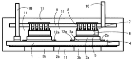
- FIG. 1 is a cross-sectional view of a principal part of a semiconductor device according to a first embodiment of the present invention.
- FIG. 2 is a plan view of an essential part of the DCB substrate of FIG.
- a semiconductor power module as a semiconductor device includes a DCB (Direct Copper Bonding) which is an insulating substrate with a conductive pattern composed of an insulating substrate 1 and copper circuit patterns 2a and 2b formed on the front and back of the insulating substrate 1.
- a substrate 4 is provided.
- the semiconductor power module also includes a copper block 3a that is fixed to the copper circuit pattern 2a of the DCB substrate 4 by diffusion bonding or the like, and a copper block 3b that is fixed to the copper circuit pattern 2b of the DCB substrate 4 by diffusion bonding or the like.
- the semiconductor power module includes a semiconductor chip 6 whose back surface is fixed to the copper block 3a with a bonding material 5 such as solder, a conductive post 8 fixed to the upper surface electrode of the semiconductor chip 6 with a bonding material 7 such as solder, And a printed circuit board 9 having the conductive posts 8. Furthermore, in this semiconductor power module, the external lead-out terminals 10 are fixed to the copper block 3a and the printed board 9 with a bonding material (not shown). Furthermore, the semiconductor power module includes a sealing resin 11 that seals the semiconductor chip 6, the DCB substrate 4, and the printed board 9. From the sealing resin 11, the end part of the external lead-out terminal 10 and one main surface of the copper block 3b are exposed.
- the copper circuit pattern 2 a has a circular cross-sectional shape when seen in a plan view, and a plurality of small drill holes 12 a opened to the position of the surface of the insulating substrate 1 are arranged. These drill holes 12a are arranged so that the number per unit area increases as the distance from the end of the copper block 3a increases, thereby reducing the volume of the copper film per unit area of the copper circuit pattern 2a. It is decreasing towards the outside.
- the average area density So is decreased outward from the copper block.
- the resin 11 is filled in the hole 12a formed in the copper circuit pattern 2a and cured.
- the resin 11 is cured, in addition to adhesion by chemical bonding between the resin 11 and a member (for example, the copper circuit pattern 2a), the resin 11 is physically peeled by being cured after the hole 11a is filled with the resin 11. It becomes difficult (anchor effect).
- the area (or volume) of the copper circuit pattern portion is reduced in the portion where the apparent perforated holes 12 a are large, and the volume of the copper film of the copper circuit pattern occupied in the ceramic forming the insulating substrate 1. Becomes smaller. Therefore, the linear expansion coefficient of the copper circuit pattern is close to that of the insulating substrate. Further, the area (or volume) of the copper circuit pattern 2a is large in the portion where the perforated holes 12a are small, the copper volume of the copper circuit pattern occupying the ceramic is large, and the linear expansion coefficient of the copper circuit pattern is close to copper.
- the copper area (or volume) in the vicinity of the ceramic (the copper circuit pattern 2a away from the copper block 3a) is reduced, and the copper area (or volume) in the vicinity of the copper block 3a is increased.
- the difference in the linear expansion coefficient between the copper circuit pattern 2a and the ceramic that is the insulating substrate 1 becomes gradual, and the stress concentration between the copper circuit pattern near the insulating substrate and the sealing resin by the heat around the semiconductor chip serving as the heat source is reduced.
- separation of the resin 11 is prevented in combination with the anchor effect of the drilled hole 12a. Further, insulation failure due to ceramic cracking is suppressed, and high reliability can be realized.
- perforated holes may be similarly formed in the copper circuit pattern 2b on the back side where the semiconductor chip 6 is not mounted.
- the semiconductor device is used so that one main surface of the copper block 3b is in contact with the cooler, and the periphery of the copper block 3b is lower in temperature than the periphery of the copper block 3a to which the semiconductor chip 6 is fixed.
- the area occupied by the pattern 2b on the insulating substrate 1 is large, the difference in the linear expansion coefficient between the copper circuit patterns 2a and 2b and the insulating substrate 1 can be reduced as a whole by forming the pattern 2b on both the copper circuit patterns 2a and 2b, and further reliability. Can be improved.
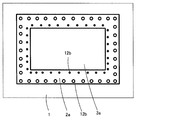
- FIG. 4 is a plan view of the main part of the semiconductor device according to the second embodiment of the present invention. This figure is a plan view of the main part of the DCB substrate 4 constituting the semiconductor device. This plan view is a plan view corresponding to FIG.
- the difference from FIG. 2 is that the number of holes 12b (area of the cross section) is changed by making the number per unit area substantially the same.
- the effect similar to Example 1 is acquired by making the drilling hole 12b small in the copper block 3a vicinity, and enlarging the drilling hole 12b of the distant place.
- FIG. 6 is a plan view of the main part of the semiconductor device according to the third embodiment of the present invention. This figure is a plan view of the main part of the DCB substrate 4 constituting the semiconductor device. This plan view is a plan view corresponding to FIG.
- the difference from FIG. 2 is that the formed drilling hole 12a is changed to an annular drilling groove 12d.
- the area of copper near the ceramic away from the copper block can be reduced.
- the effect similar to Example 1 is acquired by making small and enlarging the copper area of the copper block vicinity. As shown in FIG. 7, the same effect can be obtained even if the width of each of the drilling grooves 12e is increased outward.
- annular drilling grooves 12d and 12e may have the shape interrupted on the way irrespective of the cyclic
- FIGS. 9A and 9B are a plan view (a) and a cross-sectional view (b) of the main part of the DCB substrate of the semiconductor device according to the fourth embodiment of the present invention. The difference from FIG. 2 is that the thickness of the copper circuit pattern 2a is changed instead of forming the drilled hole.
- a similar effect can be obtained by the slope-like copper circuit pattern 14 whose thickness is gradually decreased at a constant rate toward the outside. Further, the same effect can be obtained even if the stepped copper circuit pattern 15 is thinned in a step shape instead of a slope shape as shown in FIG. Although not shown in the figure, when the drilling holes or the annular drilling grooves are uniformly arranged in this structure, an anchor effect is generated, so that the adhesion of the resin 11 is further improved.
Abstract
Provided is a resin-sealed semiconductor device capable of maintaining sealing resin adhesion and of increasing module reliability. This semiconductor device is provided with an insulating substrate with conductive pattern (1), conductive blocks (3a, 3b) fixed on the conductive patterns (2a, 2b) of the insulating substrate (1), a semiconductor chip (6) fixed on the conductive block, a print substrate (9) having conductive posts (8) fixed on the semiconductor chip, and a resin (11) which seals these. The average volume of the conductive film per unit surface area of the conductive pattern around the position where the conductive block is fixed decreases outwards from the conductive block.
Description
この発明は、パワー半導体モジュールなどの半導体装置に関する。
The present invention relates to a semiconductor device such as a power semiconductor module.
図11は、特許文献1に記載の構造と類似の構造をした従来の半導体装置の要部断面図である。従来の半導体装置であるパワー半導体モジュールは、絶縁基板101とこの絶縁基板101の表裏に形成される銅回路パターン102a,102bで構成される導電パターン付絶縁基板であるDCB(Direct Copper Bonding)基板104を備える。また、このパワー半導体モジュールは、DCB基板104の銅回路パターン102aに拡散接合等で固着する銅ブロック103aと、DCB基板104の銅回路パターン102bに拡散接合等で固着する銅ブロック103bを備える。さらに、このパワー半導体モジュールは、銅ブロック103a上に半田などの接合材105で裏面が固着する半導体チップ106と、半導体チップ106の上面電極に半田などの接合材107で固着する導電ポスト108と、この導電ポスト108を有するプリント基板109とを備える。さらにまた、このパワー半導体モジュールは、前記の半導体チップ106およびDCB基板104およびプリント基板109を封止する封止樹脂111を備える。符号110は、外部導出端子を示す。
FIG. 11 is a cross-sectional view of a main part of a conventional semiconductor device having a structure similar to the structure described in Patent Document 1. A power semiconductor module which is a conventional semiconductor device includes a DCB (Direct Copper Bonding) substrate 104 which is an insulating substrate with a conductive pattern composed of an insulating substrate 101 and copper circuit patterns 102a and 102b formed on the front and back of the insulating substrate 101. Is provided. The power semiconductor module also includes a copper block 103a that is fixed to the copper circuit pattern 102a of the DCB substrate 104 by diffusion bonding or the like, and a copper block 103b that is fixed to the copper circuit pattern 102b of the DCB substrate 104 by diffusion bonding or the like. Further, this power semiconductor module includes a semiconductor chip 106 whose back surface is fixed to the copper block 103a with a bonding material 105 such as solder, and a conductive post 108 fixed to the upper surface electrode of the semiconductor chip 106 with a bonding material 107 such as solder, And a printed circuit board 109 having the conductive posts 108. Furthermore, the power semiconductor module includes a sealing resin 111 that seals the semiconductor chip 106, the DCB substrate 104, and the printed circuit board 109. Reference numeral 110 denotes an external lead-out terminal.
また、特許文献2では、DCB基板にパワー半導体チップを半田接合するときに、セラミック基板との境界部分に沿う導体パターンの縁部に複数の応力緩和用のディンブルを設けることが記載されている。
In Patent Document 2, it is described that when a power semiconductor chip is solder-bonded to a DCB substrate, a plurality of stress relaxation dimples are provided at the edge of the conductor pattern along the boundary portion with the ceramic substrate.
さらに、特許文献3では、放熱基体に繰り返し与えられる熱応力を低減するために、回路部材と支持基体を接合するための金属層の外周縁部に平面視で凹凸を形成することが記載されている。
Furthermore, Patent Document 3 describes that irregularities are formed in a plan view on the outer peripheral edge of a metal layer for joining a circuit member and a support base in order to reduce thermal stress repeatedly applied to the heat dissipation base. Yes.
さらにまた、特許文献4では、セラミックス基板に銅板等の金属板を、直接接合法や活性金属法等で接合して構成したセラミックス回路基板において、銅板の接合面と反対面側の外周縁部内側に、例えば外周縁部に沿って所定の間隔で直線状に不連続な溝を形成している。こうすることで、冷熱サイクルが付加された場合等においても、セラミックス基板のクラック発生や強度低下を有効に防止することができることが記載されている。
Furthermore, in Patent Document 4, in a ceramic circuit board formed by bonding a metal plate such as a copper plate to a ceramic substrate by a direct bonding method, an active metal method, or the like, the inner side of the outer peripheral edge on the side opposite to the bonding surface of the copper plate In addition, for example, linearly discontinuous grooves are formed at predetermined intervals along the outer peripheral edge. By doing so, it is described that cracking and strength reduction of the ceramic substrate can be effectively prevented even when a cooling cycle is added.
樹脂封止型半導体においては、内蔵される部材との樹脂密着性が信頼性に大きく影響を与える。図11の構造においては、DCB基板104を構成するセラミックからなる絶縁基板101と、銅で形成される銅回路パターン102a,102bとの線膨張率差が原因となり、絶縁基板101近傍の銅回路パターン102a,102bと封止樹脂111の間で応力が発生し、DCB基板104と封止樹脂111との間に剥離が生じるという課題があった。
In resin-encapsulated semiconductors, resin adhesion with built-in members greatly affects reliability. In the structure of FIG. 11, the copper circuit pattern in the vicinity of the insulating substrate 101 is caused by the difference in linear expansion coefficient between the insulating substrate 101 made of ceramic constituting the DCB substrate 104 and the copper circuit patterns 102a and 102b formed of copper. There is a problem that stress is generated between the sealing resin 111 a and the sealing resin 111, and peeling occurs between the DCB substrate 104 and the sealing resin 111.
半導体チップ106が搭載されるDCB基板104と封止樹脂111との間に剥離が進行した場合、半導体チップ106と銅ブロック103aとの接合部にも応力が集中し、接合部劣化が発生して、故障の原因となる。
When peeling progresses between the DCB substrate 104 on which the semiconductor chip 106 is mounted and the sealing resin 111, stress is concentrated on the joint between the semiconductor chip 106 and the copper block 103a, and the joint is deteriorated. Cause failure.
特に、銅回路パターン102aと封止樹脂111との間に生じた剥離が絶縁基板101にまで進展すると、絶縁不良が発生する。また、封止樹脂111が絶縁基板101とのみ密着し、銅回路パターン102aから剥離している状態でも、銅回路パターン102a近傍の絶縁基板101に応力が集中するため、絶縁基板101にクラックが発生し、同様に絶縁不良となる。
In particular, when the peeling that occurs between the copper circuit pattern 102a and the sealing resin 111 progresses to the insulating substrate 101, an insulation failure occurs. In addition, even when the sealing resin 111 is in close contact with the insulating substrate 101 and peeled off from the copper circuit pattern 102a, the stress is concentrated on the insulating substrate 101 near the copper circuit pattern 102a, so that the insulating substrate 101 is cracked. In the same manner, insulation failure occurs.
さらに、近年適用が進むSiC(炭化珪素)デバイス等のWBG(ワイドバンドギャップ)素子を搭載したパワー半導体モジュールでは、動作温度範囲が従来のSi(シリコン)デバイスを搭載したパワー半導体モジュールと比べ高くなっており、Siデバイスを搭載したパワー半導体モジュール以上(Tjmax≧175℃)の高温駆動となる。そのような場合、さらに熱応力が増大するため、前記のような封止樹脂111の剥離が起こりやすくなることが想定され、信頼性の低下が懸念される。
Furthermore, power semiconductor modules equipped with WBG (wide band gap) elements such as SiC (silicon carbide) devices, which have been increasingly applied in recent years, have a higher operating temperature range than power semiconductor modules equipped with conventional Si (silicon) devices. Therefore, it is driven at a high temperature higher than that of a power semiconductor module equipped with a Si device (Tjmax ≧ 175 ° C.). In such a case, since the thermal stress further increases, it is assumed that the sealing resin 111 as described above is likely to be peeled off, and there is a concern about a decrease in reliability.
前記の特許文献1~特許文献4では、銅ブロックの周囲の銅回路パターンの銅の平均の体積を銅ブロックから外に向って小さくすることで、銅回路パターンと絶縁基板との線膨張率差を緩やかにして、熱応力集中を回避し、樹脂の剥離を生じにくくすることについては記載されていない。
In Patent Documents 1 to 4, the difference in linear expansion coefficient between the copper circuit pattern and the insulating substrate is reduced by reducing the average volume of copper in the copper circuit pattern around the copper block outward from the copper block. There is no description about relaxing the resin to avoid concentration of thermal stress and to prevent the resin from peeling off.
この発明の目的は、前記の課題を解決して、樹脂封止型パワー半導体モジュールなどの半導体装置において、封止樹脂の密着性を保持し、モジュールの信頼性および寿命を向上させることができる半導体装置を提供することにある。
The object of the present invention is to solve the above-mentioned problems and maintain the adhesion of the sealing resin in a semiconductor device such as a resin-encapsulated power semiconductor module, thereby improving the reliability and life of the module. To provide an apparatus.
前記の目的を達成するために、本発明は、導電パターン付絶縁基板(例えば、DCB基板など)と、該導電パターン付絶縁基板の導電パターン(例えば、回路パターンなど)上に固着された導電ブロック(例えば、銅ブロックなど)と、該導電ブロック上に固着された半導体チップと、該半導体チップ上に固着された導電ポストを備えるプリント基板と、これらを封止する樹脂(封止樹脂)とを備えている半導体装置において、前記導電ブロックが固着した箇所の周囲の前記導電パターンの単位面積あたりの平均の導電膜の体積を、該導電ブロックから外に向って減少するように配置した構成とする。
In order to achieve the above object, the present invention provides an insulating substrate with a conductive pattern (for example, a DCB substrate) and a conductive block fixed on the conductive pattern (for example, a circuit pattern) of the insulating substrate with a conductive pattern. (For example, a copper block), a semiconductor chip fixed on the conductive block, a printed board including a conductive post fixed on the semiconductor chip, and a resin (sealing resin) for sealing them The semiconductor device is provided with a configuration in which the volume of the average conductive film per unit area of the conductive pattern around the portion where the conductive block is fixed is arranged so as to decrease outward from the conductive block. .
また、本発明によれば、前記導電ブロックが固着した箇所の周囲の前記導電パターンに、該導電ブロックから外に向って単位面積あたりの個数が増加するように穿設穴を配置して、前記導電パターンの導電膜の体積を減少させるとよい。
According to the present invention, in the conductive pattern around the portion where the conductive block is fixed, a perforation hole is arranged so that the number per unit area increases outward from the conductive block, It is preferable to reduce the volume of the conductive film of the conductive pattern.
また、本発明によれば、前記導電ブロックが固着した箇所の周囲の前記導電パターンに、該導電ブロックから外に向って断面の面積が大きくなる穿設穴を配置して、前記導電パターンの導電膜の体積を減少させるとよい。
Further, according to the present invention, the conductive pattern around the portion where the conductive block is fixed is provided with a perforated hole having a cross-sectional area that increases outward from the conductive block, so that the conductive pattern is electrically conductive. It is good to reduce the volume of the membrane.
また、本発明によれば、前記導電ブロックが固着した箇所の周囲の前記導電パターンに、該導電ブロックから外に向って単位長さあたりの本数が増加する環状の穿設溝を配置して、前記導電パターンの導電膜の体積を減少させるとよい。
Further, according to the present invention, in the conductive pattern around the portion where the conductive block is fixed, an annular perforated groove whose number per unit length increases outward from the conductive block is arranged, The volume of the conductive film of the conductive pattern may be reduced.
また、本発明によれば、前記導電ブロックが固着した箇所の周囲の前記導電パターンに、該導電ブロックから外に向って幅が増加する環状の穿設溝を配置して、前記導電パターンの導電膜の体積を減少させるとよい。
Further, according to the present invention, an annular perforated groove having a width increasing outwardly from the conductive block is disposed in the conductive pattern around the portion where the conductive block is fixed, so that the conductive pattern is electrically conductive. It is good to reduce the volume of the membrane.
また、本発明によれば、前記穿設穴もしくは前記環状の穿設溝の底部を、前記導電膜により塞いでもよい。
Further, according to the present invention, the bottom of the perforated hole or the annular perforated groove may be closed with the conductive film.
また、本発明によれば、前記導電ブロックが固着した箇所の周囲の前記導電パターンの厚さを該導電ブロックから外に向って徐々に薄くすることで、前記導電パターンの導電膜の体積を減少させるとよい。
In addition, according to the present invention, the volume of the conductive film of the conductive pattern is reduced by gradually reducing the thickness of the conductive pattern around the portion where the conductive block is fixed outward from the conductive block. It is good to let them.
また、本発明によれば、前記導電ブロックが固着した箇所の周囲の前記導電パターンに、穿設穴もしくは環状の穿設溝を設けるとよい。
Further, according to the present invention, it is preferable to provide a drill hole or an annular drill groove in the conductive pattern around the portion where the conductive block is fixed.
また、本発明によれば、厚さが徐々に薄くなる前記導電パターンの断面形状が、スロープ状もしくは階段状であるとよい。
In addition, according to the present invention, it is preferable that the cross-sectional shape of the conductive pattern whose thickness is gradually reduced is a slope shape or a step shape.
また、本発明によれば、前記導電パターン付絶縁基板の表(おもて)面側に前記導電パターンが接合され、該導電パターン上に前記導電ブロックおよび前記半導体チップが順に固着されており、かつ、前記導電パターン付絶縁基板の裏面側に他の導電パターンが接合され、該他の導電パターン上に他の導電ブロックが固着されており、前記他の導電ブロックの一の主面が前記樹脂から露出しているとよい。
Further, according to the present invention, the conductive pattern is bonded to the front surface side of the insulating substrate with a conductive pattern, and the conductive block and the semiconductor chip are fixed in order on the conductive pattern, And another conductive pattern is joined to the back side of the insulating substrate with the conductive pattern, and another conductive block is fixed on the other conductive pattern, and one main surface of the other conductive block is the resin. It is good to be exposed from.
また、本発明によれば、前記導電パターンおよび他の導電パターンが金属膜であり、前記導電ブロックおよび他の導電ブロックが金属ブロックであるとよい。
Further, according to the present invention, the conductive pattern and the other conductive pattern may be a metal film, and the conductive block and the other conductive block may be a metal block.
本発明によれば、導電ブロックが固着した導電パターン付絶縁基板の導電パターンにおいて、導電ブロックが固着した箇所の周囲の導電パターンの単位面積あたりの平均の体積を導電ブロックから外に向って減少させるように配置したことで、導電パターン付絶縁基板と封止樹脂の密着性を向上させ、半導体装置の信頼性および寿命を向上させることができる。
According to the present invention, in the conductive pattern of the insulating substrate with a conductive pattern to which the conductive block is fixed, the average volume per unit area of the conductive pattern around the portion where the conductive block is fixed is decreased outward from the conductive block. By arrange | positioning in this way, the adhesiveness of the insulating substrate with a conductive pattern and sealing resin can be improved, and the reliability and lifetime of a semiconductor device can be improved.
本発明を実施するための形態のポイントは、銅ブロックの周囲の銅回路パターンの銅の単位面積あたりの平均の体積を外に向って小さくすることで、銅回路パターンと絶縁基板との線膨張率差を緩やかにして、熱応力集中を回避し、樹脂の剥離を生じにくくすることである。平均の体積を減少させる方法としては、穿設穴の配置密度や、環状の穿設溝の占める面積、厚さなどを変える方法がある。また、穿設穴や環状の穿設溝を形成することでアンカー効果が出てきて、さらに樹脂の剥離が生じにくくなる。実施の形態を以下の実施例で説明する。
<実施例1>
図1は、本発明の第1実施例における半導体装置の要部断面図である。 The point of the embodiment for carrying out the present invention is that the average volume per unit area of copper of the copper circuit pattern around the copper block is decreased outwardly, thereby linear expansion of the copper circuit pattern and the insulating substrate. It is to reduce the rate difference, avoid concentration of thermal stress, and make it difficult for the resin to peel off. As a method of reducing the average volume, there is a method of changing the arrangement density of the drilling holes, the area occupied by the annular drilling groove, the thickness, and the like. In addition, the anchor effect can be obtained by forming the perforated hole or the annular perforated groove, and the resin is hardly peeled off. Embodiments will be described in the following examples.
<Example 1>
FIG. 1 is a cross-sectional view of a principal part of a semiconductor device according to a first embodiment of the present invention.
図2は、図1のDCB基板の要部平面図である。
図1において、半導体装置である半導体パワーモジュールは、絶縁基板1とこの絶縁基板1の表裏に形成される銅回路パターン2a,2bで構成される導電パターン付絶縁基板であるDCB(Direct Copper Bonding)基板4を備える。また、この半導体パワーモジュールは、DCB基板4の銅回路パターン2aに拡散接合等で固着する銅ブロック3aと、DCB基板4の銅回路パターン2bに拡散接合等で固着する銅ブロック3bを備える。さらに、この半導体パワーモジュールは、銅ブロック3a上に半田などの接合材5で裏面が固着する半導体チップ6と、半導体チップ6の上面電極に半田などの接合材7で固着する導電ポスト8と、この導電ポスト8を有するプリント基板9とを備える。さらにまた、この半導体パワーモジュールにおいて、銅ブロック3aとプリント基板9にはそれぞれ、外部導出端子10が、図示しない接合材により固着されている。さらにまた、この半導体パワーモジュールは、前記の半導体チップ6およびDCB基板4およびプリント基板9を封止する封止樹脂11を備える。封止樹脂11からは、外部導出端子10の端部と銅ブロック3bの一の主面が露出している。 FIG. 2 is a plan view of an essential part of the DCB substrate of FIG.
In FIG. 1, a semiconductor power module as a semiconductor device includes a DCB (Direct Copper Bonding) which is an insulating substrate with a conductive pattern composed of an insulatingsubstrate 1 and copper circuit patterns 2a and 2b formed on the front and back of the insulating substrate 1. A substrate 4 is provided. The semiconductor power module also includes a copper block 3a that is fixed to the copper circuit pattern 2a of the DCB substrate 4 by diffusion bonding or the like, and a copper block 3b that is fixed to the copper circuit pattern 2b of the DCB substrate 4 by diffusion bonding or the like. Further, the semiconductor power module includes a semiconductor chip 6 whose back surface is fixed to the copper block 3a with a bonding material 5 such as solder, a conductive post 8 fixed to the upper surface electrode of the semiconductor chip 6 with a bonding material 7 such as solder, And a printed circuit board 9 having the conductive posts 8. Furthermore, in this semiconductor power module, the external lead-out terminals 10 are fixed to the copper block 3a and the printed board 9 with a bonding material (not shown). Furthermore, the semiconductor power module includes a sealing resin 11 that seals the semiconductor chip 6, the DCB substrate 4, and the printed board 9. From the sealing resin 11, the end part of the external lead-out terminal 10 and one main surface of the copper block 3b are exposed.
図1において、半導体装置である半導体パワーモジュールは、絶縁基板1とこの絶縁基板1の表裏に形成される銅回路パターン2a,2bで構成される導電パターン付絶縁基板であるDCB(Direct Copper Bonding)基板4を備える。また、この半導体パワーモジュールは、DCB基板4の銅回路パターン2aに拡散接合等で固着する銅ブロック3aと、DCB基板4の銅回路パターン2bに拡散接合等で固着する銅ブロック3bを備える。さらに、この半導体パワーモジュールは、銅ブロック3a上に半田などの接合材5で裏面が固着する半導体チップ6と、半導体チップ6の上面電極に半田などの接合材7で固着する導電ポスト8と、この導電ポスト8を有するプリント基板9とを備える。さらにまた、この半導体パワーモジュールにおいて、銅ブロック3aとプリント基板9にはそれぞれ、外部導出端子10が、図示しない接合材により固着されている。さらにまた、この半導体パワーモジュールは、前記の半導体チップ6およびDCB基板4およびプリント基板9を封止する封止樹脂11を備える。封止樹脂11からは、外部導出端子10の端部と銅ブロック3bの一の主面が露出している。 FIG. 2 is a plan view of an essential part of the DCB substrate of FIG.
In FIG. 1, a semiconductor power module as a semiconductor device includes a DCB (Direct Copper Bonding) which is an insulating substrate with a conductive pattern composed of an insulating
図2に示すように、銅回路パターン2aには、平面視したときの断面形状が円形であり、絶縁基板1の表面の位置まで開口した小さな穿設穴12aが複数配置されている。これらの穿設穴12aは、銅ブロック3aの端部から外に向かって離れるにつれて、単位面積あたりの個数を増やすように配置することで、銅回路パターン2aの単位面積あたりの銅膜の体積を外に向かって減少させている。
As shown in FIG. 2, the copper circuit pattern 2 a has a circular cross-sectional shape when seen in a plan view, and a plurality of small drill holes 12 a opened to the position of the surface of the insulating substrate 1 are arranged. These drill holes 12a are arranged so that the number per unit area increases as the distance from the end of the copper block 3a increases, thereby reducing the volume of the copper film per unit area of the copper circuit pattern 2a. It is decreasing towards the outside.
このように、銅回路パターン2aに形成される穿設穴12aの数を銅ブロック3aから外に向かって離れるにつれて増加させることで、銅膜の平均の体積密度は外に向って減少する。平均の体積密度とは、銅ブロックを一周する穿設穴12aの中央線20の長さをL、所定の幅(例えば、穿設穴の直径の1倍超の幅)をW、環状の帯の面積S1、穿設穴12aの面積をS2、環状の面積S1に存在する穿設穴12aの数をn、環状の面積S1に存在する穿設穴12aの総面積をS3、銅の平均の面積密度Soとしたとき、S1=L×W、S3=S2×nであり、So=(S1-S3)/S1となる。この平均の面積密度Soを銅ブロックから外に向って小さくする。このSoに銅回路パターン12aの厚さtを掛けたもの(So×t)が平均の体積密度Voとなり、この平均の体積密度Voを銅ブロック3aから外に向って離れるにつれて小さくする。
Thus, by increasing the number of perforated holes 12a formed in the copper circuit pattern 2a toward the outside from the copper block 3a, the average volume density of the copper film decreases outward. The average volume density means that the length of the center line 20 of the drilled hole 12a that goes around the copper block is L, a predetermined width (for example, a width that is more than 1 times the diameter of the drilled hole), W, and an annular belt Area S1, the area of the hole 12a is S2, the number of holes 12a existing in the annular area S1 is n, the total area of the holes 12a existing in the annular area S1 is S3, the average of copper When the area density is So, S1 = L × W, S3 = S2 × n, and So = (S1−S3) / S1. The average area density So is decreased outward from the copper block. This So multiplied by the thickness t of the copper circuit pattern 12a (So × t) becomes the average volume density Vo, and this average volume density Vo is reduced as it goes away from the copper block 3a.
樹脂封止することにより、銅回路パターン2aに形成される穿設穴12aに樹脂11が充填され硬化する。樹脂11が硬化することで、樹脂11と部材(例えば、銅回路パターン2a)の化学的結合による接着に加え、穿設穴12aに樹脂11が充填された後に硬化することで、物理的に剥がれにくくなる(アンカー効果)。
By sealing with resin, the resin 11 is filled in the hole 12a formed in the copper circuit pattern 2a and cured. When the resin 11 is cured, in addition to adhesion by chemical bonding between the resin 11 and a member (for example, the copper circuit pattern 2a), the resin 11 is physically peeled by being cured after the hole 11a is filled with the resin 11. It becomes difficult (anchor effect).
さらに、DCB基板4全体では、見かけ上の穿設穴12aが多い部分は銅回路パターン部分の面積(または体積)が小さくなり、絶縁基板1を形成するセラミックに占める銅回路パターンの銅膜の体積が小さくなる。そのため、銅回路パターンの線膨張率は絶縁基板に近くなる。また、穿設穴12aが少ない部分は銅回路パターン2aの面積(または体積)が大きく、セラミックに占める銅回路パターンの銅の体積が大きくなり、銅回路パターンの線膨張率は銅に近くなる。
Further, in the entire DCB substrate 4, the area (or volume) of the copper circuit pattern portion is reduced in the portion where the apparent perforated holes 12 a are large, and the volume of the copper film of the copper circuit pattern occupied in the ceramic forming the insulating substrate 1. Becomes smaller. Therefore, the linear expansion coefficient of the copper circuit pattern is close to that of the insulating substrate. Further, the area (or volume) of the copper circuit pattern 2a is large in the portion where the perforated holes 12a are small, the copper volume of the copper circuit pattern occupying the ceramic is large, and the linear expansion coefficient of the copper circuit pattern is close to copper.
そのため、セラミック付近(銅ブロック3aから外の方へ離れた箇所の銅回路パターン2a)の銅の面積(または体積)を小さくし、銅ブロック3a付近の銅の面積(または体積)を大きくすることで、銅回路パターン2aと絶縁基板1であるセラミックの線膨張率差が緩やかとなり、熱源となる半導体チップ周辺での、熱による絶縁基板近傍の銅回路パターンと封止樹脂の間の応力集中を回避できる。その結果、穿設穴12aのアンカー効果と相まって樹脂11の剥離が防止される。また、セラミックの割れによる絶縁不良が抑制されて、高い信頼性を実現することができる。
Therefore, the copper area (or volume) in the vicinity of the ceramic (the copper circuit pattern 2a away from the copper block 3a) is reduced, and the copper area (or volume) in the vicinity of the copper block 3a is increased. Thus, the difference in the linear expansion coefficient between the copper circuit pattern 2a and the ceramic that is the insulating substrate 1 becomes gradual, and the stress concentration between the copper circuit pattern near the insulating substrate and the sealing resin by the heat around the semiconductor chip serving as the heat source is reduced. Can be avoided. As a result, separation of the resin 11 is prevented in combination with the anchor effect of the drilled hole 12a. Further, insulation failure due to ceramic cracking is suppressed, and high reliability can be realized.
尚、図1には図示していないが、半導体チップ6が搭載されない裏面側の銅回路パターン2bにも、同様に穿設穴を形成してもよい。半導体装置は銅ブロック3bの一の主面が冷却器に接触するように使用され、銅ブロック3bの周辺は、半導体チップ6が固着した銅ブロック3aの周辺に比べれば低温となるが、銅回路パターン2bの絶縁基板1に占める面積が大きい場合には、銅回路パターン2a,2b両方に形成することにより銅回路パターン2a,2bと絶縁基板1の線膨張率差を全体として小さくでき、さらに信頼性を向上できる。
Although not shown in FIG. 1, perforated holes may be similarly formed in the copper circuit pattern 2b on the back side where the semiconductor chip 6 is not mounted. The semiconductor device is used so that one main surface of the copper block 3b is in contact with the cooler, and the periphery of the copper block 3b is lower in temperature than the periphery of the copper block 3a to which the semiconductor chip 6 is fixed. When the area occupied by the pattern 2b on the insulating substrate 1 is large, the difference in the linear expansion coefficient between the copper circuit patterns 2a and 2b and the insulating substrate 1 can be reduced as a whole by forming the pattern 2b on both the copper circuit patterns 2a and 2b, and further reliability. Can be improved.
また、図3に示すように、穿設穴12aの個数を増やすことでアンカー効果が増進され、一層樹脂11の剥離が防止される。
<実施例2>
図4は、本発明の第2実施例における半導体装置の要部平面図である。この図は半導体装置を構成するDCB基板4の要部平面図である。この平面図は図2に相当する平面図である。 Further, as shown in FIG. 3, the anchor effect is enhanced by increasing the number of theperforated holes 12a, and the resin 11 is further prevented from peeling off.
<Example 2>
FIG. 4 is a plan view of the main part of the semiconductor device according to the second embodiment of the present invention. This figure is a plan view of the main part of theDCB substrate 4 constituting the semiconductor device. This plan view is a plan view corresponding to FIG.
<実施例2>
図4は、本発明の第2実施例における半導体装置の要部平面図である。この図は半導体装置を構成するDCB基板4の要部平面図である。この平面図は図2に相当する平面図である。 Further, as shown in FIG. 3, the anchor effect is enhanced by increasing the number of the
<Example 2>
FIG. 4 is a plan view of the main part of the semiconductor device according to the second embodiment of the present invention. This figure is a plan view of the main part of the
図2との違いは、単位面積あたりの個数をほぼ同じにして穿設穴12bのそれぞれの大きさ(断面の面積)を変えた点である。銅ブロック3a近傍で穿設穴12bを小さくし、離れた箇所の穿設穴12bを大きくすることで、実施例1と同様の効果が得られる。
The difference from FIG. 2 is that the number of holes 12b (area of the cross section) is changed by making the number per unit area substantially the same. The effect similar to Example 1 is acquired by making the drilling hole 12b small in the copper block 3a vicinity, and enlarging the drilling hole 12b of the distant place.
尚、実施例1、実施例2ともに穿設穴12a,12bの形状は円形であるが、これに限られるものではなく、図5に示すような矩形の穿設穴12c等にしても構わない。また、矩形と円形の組み合わせでも構わない。
<実施例3>
図6は、本発明の第3実施例における半導体装置の要部平面図である。この図は半導体装置を構成するDCB基板4の要部平面図である。この平面図は図2に相当する平面図である。 In both the first and second embodiments, the shape of the drill holes 12a and 12b is circular. However, the shape is not limited to this, and arectangular drill hole 12c as shown in FIG. 5 may be used. . A combination of a rectangle and a circle may be used.
<Example 3>
FIG. 6 is a plan view of the main part of the semiconductor device according to the third embodiment of the present invention. This figure is a plan view of the main part of theDCB substrate 4 constituting the semiconductor device. This plan view is a plan view corresponding to FIG.
<実施例3>
図6は、本発明の第3実施例における半導体装置の要部平面図である。この図は半導体装置を構成するDCB基板4の要部平面図である。この平面図は図2に相当する平面図である。 In both the first and second embodiments, the shape of the drill holes 12a and 12b is circular. However, the shape is not limited to this, and a
<Example 3>
FIG. 6 is a plan view of the main part of the semiconductor device according to the third embodiment of the present invention. This figure is a plan view of the main part of the
図2との違いは、形成する穿設穴12aを環状の穿設溝12dに変えた点である。環状の穿設溝12dの、銅ブロック3aから外に向かう方向における単位長さあたりの本数を外に向かって密にする(大きくする)ことで、銅ブロックから離れたセラミック付近の銅の面積を小さくし、銅ブロック付近の銅の面積を大きくすることで、実施例1と同様の効果が得られる。図7に示すように、穿設溝12eのそれぞれの幅を外に向って広くしても同様の効果が得られる。また、図示しないが、環状の穿設溝12d,12eは、環状によらず途中で途切れた形状等でもよく、部分的に穿設溝が形成されている箇所があっても構わない。
The difference from FIG. 2 is that the formed drilling hole 12a is changed to an annular drilling groove 12d. By increasing the number of annular perforated grooves 12d per unit length in the direction outward from the copper block 3a toward the outside (enlarging), the area of copper near the ceramic away from the copper block can be reduced. The effect similar to Example 1 is acquired by making small and enlarging the copper area of the copper block vicinity. As shown in FIG. 7, the same effect can be obtained even if the width of each of the drilling grooves 12e is increased outward. Moreover, although not shown in figure, the cyclic | annular drilling grooves 12d and 12e may have the shape interrupted on the way irrespective of the cyclic | annular form, and may have the location in which the drilling groove is partially formed.
前記実施例1~実施例3において、図8の断面図に示すように、穿設穴12hもしくは環状の穿設溝12jを絶縁基板1の表面の位置まで貫通させないで薄い銅層を底部13に残した構造としても同様の効果が得られる。また、残す銅層の厚さを銅ブロック3aから外に向って徐々に薄くしても同様の効果が得られる。
<実施例4>
図9は、本発明の第4実施例における半導体装置のDCB基板の要部平面図(a)および要部断面図(b)である。図2との違いは、穿設穴を形成するのではなく、銅回路パターン2aの厚さを変えた点である。厚さを外に向って一定の割合で徐々に薄くしたスロープ状銅回路パターン14により、同様の効果が得られる。また、図10のようにスロープ状でなく階段状に薄くした階段状銅回路パターン15にしても同様の効果が得られる。また、図示しないが、この構造に穿設穴もしくは環状の穿設溝を均一に配置すると、アンカー効果が発生するため、樹脂11の密着性はさらに向上する。 In the first to third embodiments, as shown in the cross-sectional view of FIG. 8, a thin copper layer is not formed on thebottom portion 13 without penetrating the hole 12h or the annular hole 12j to the position of the surface of the insulating substrate 1. The same effect can be obtained with the remaining structure. Further, the same effect can be obtained even if the thickness of the remaining copper layer is gradually reduced from the copper block 3a toward the outside.
<Example 4>
FIGS. 9A and 9B are a plan view (a) and a cross-sectional view (b) of the main part of the DCB substrate of the semiconductor device according to the fourth embodiment of the present invention. The difference from FIG. 2 is that the thickness of thecopper circuit pattern 2a is changed instead of forming the drilled hole. A similar effect can be obtained by the slope-like copper circuit pattern 14 whose thickness is gradually decreased at a constant rate toward the outside. Further, the same effect can be obtained even if the stepped copper circuit pattern 15 is thinned in a step shape instead of a slope shape as shown in FIG. Although not shown in the figure, when the drilling holes or the annular drilling grooves are uniformly arranged in this structure, an anchor effect is generated, so that the adhesion of the resin 11 is further improved.
<実施例4>
図9は、本発明の第4実施例における半導体装置のDCB基板の要部平面図(a)および要部断面図(b)である。図2との違いは、穿設穴を形成するのではなく、銅回路パターン2aの厚さを変えた点である。厚さを外に向って一定の割合で徐々に薄くしたスロープ状銅回路パターン14により、同様の効果が得られる。また、図10のようにスロープ状でなく階段状に薄くした階段状銅回路パターン15にしても同様の効果が得られる。また、図示しないが、この構造に穿設穴もしくは環状の穿設溝を均一に配置すると、アンカー効果が発生するため、樹脂11の密着性はさらに向上する。 In the first to third embodiments, as shown in the cross-sectional view of FIG. 8, a thin copper layer is not formed on the
<Example 4>
FIGS. 9A and 9B are a plan view (a) and a cross-sectional view (b) of the main part of the DCB substrate of the semiconductor device according to the fourth embodiment of the present invention. The difference from FIG. 2 is that the thickness of the
1 絶縁基板
2a,2b 銅回路パターン
3a,3b 銅ブロック
4 DCB基板
5,7 接合材
6 半導体チップ
8 導電ポスト
9 プリント基板
10 外部導出端子
11 封止樹脂
12a,b,c 穿設穴
12d,12e 環状の穿設溝
12h 底面がある穿設穴
12j 底面がある環状の穿設溝
13 底部
14 スロープ状銅回路パターン
15 階段状銅回路パターン DESCRIPTION OFSYMBOLS 1 Insulation board | substrate 2a, 2b Copper circuit pattern 3a, 3b Copper block 4 DCB board | substrate 5,7 Joining material 6 Semiconductor chip 8 Conductive post 9 Printed circuit board 10 External lead-out terminal 11 Sealing resin 12a, b, c Drilling holes 12d, 12e Annular drilling groove 12h Drilling hole with bottom surface 12j Annular drilling groove with bottom surface 13 Bottom 14 Slope copper circuit pattern 15 Stepped copper circuit pattern
2a,2b 銅回路パターン
3a,3b 銅ブロック
4 DCB基板
5,7 接合材
6 半導体チップ
8 導電ポスト
9 プリント基板
10 外部導出端子
11 封止樹脂
12a,b,c 穿設穴
12d,12e 環状の穿設溝
12h 底面がある穿設穴
12j 底面がある環状の穿設溝
13 底部
14 スロープ状銅回路パターン
15 階段状銅回路パターン DESCRIPTION OF
Claims (11)
- 導電パターン付絶縁基板と、該導電パターン付絶縁基板の導電パターン上に固着された導電ブロックと、該導電ブロック上に固着された半導体チップと、該半導体チップ上に固着された導電ポストを備えるプリント基板と、これらを封止する樹脂とを備えている半導体装置において、
前記導電ブロックが固着した箇所の周囲の前記導電パターンの単位面積あたりの平均の導電膜の体積を、該導電ブロックから外に向って減少するようにしたことを特徴とする半導体装置。 An insulating substrate with a conductive pattern, a conductive block fixed on the conductive pattern of the insulating substrate with a conductive pattern, a semiconductor chip fixed on the conductive block, and a conductive post fixed on the semiconductor chip In a semiconductor device comprising a substrate and a resin for sealing them,
A semiconductor device, wherein an average volume of a conductive film per unit area of the conductive pattern around a portion where the conductive block is fixed is decreased outward from the conductive block. - 前記導電ブロックが固着した箇所の周囲の前記導電パターンに、該導電ブロックから外に向って単位面積あたりの個数が増加するように穿設穴を配置して、前記導電パターンの導電膜の体積を減少させたことを特徴とする請求項1に記載の半導体装置。 A perforation hole is arranged in the conductive pattern around the portion where the conductive block is fixed so that the number per unit area increases outward from the conductive block, and the volume of the conductive film of the conductive pattern is increased. The semiconductor device according to claim 1, wherein the semiconductor device is reduced.
- 前記導電ブロックが固着した箇所の周囲の前記導電パターンに、該導電ブロックから外に向って断面の面積が大きくなる穿設穴を配置して、前記導電パターンの導電膜の体積を減少させたことを特徴とする請求項1に記載の半導体装置。 In the conductive pattern around the portion where the conductive block is fixed, a perforated hole having a cross-sectional area that increases outward from the conductive block is arranged to reduce the volume of the conductive film of the conductive pattern. The semiconductor device according to claim 1.
- 前記導電ブロックが固着した箇所の周囲の前記導電パターンに、該導電ブロックから外に向って単位長さあたりの本数が増加する環状の穿設溝を配置して、前記導電パターンの導電膜の体積を減少させたことを特徴とする請求項1に記載の半導体装置。 An annular perforated groove that increases in number per unit length outward from the conductive block is disposed in the conductive pattern around the portion where the conductive block is fixed, and the volume of the conductive film of the conductive pattern The semiconductor device according to claim 1, wherein:
- 前記導電ブロックが固着した箇所の周囲の前記導電パターンに、該導電ブロックから外に向って幅が増加する環状の穿設溝を配置して、前記導電パターンの導電膜の体積を減少させたことを特徴とする請求項1に記載の半導体装置。 The conductive pattern around the portion where the conductive block is fixed is provided with an annular perforated groove whose width increases outward from the conductive block to reduce the volume of the conductive film of the conductive pattern. The semiconductor device according to claim 1.
- 前記穿設穴もしくは前記環状の穿設溝の底部が、前記導電膜により塞がれていることを特徴とする請求項2に記載の半導体装置。 3. The semiconductor device according to claim 2, wherein a bottom of the drilled hole or the annular drilled groove is closed by the conductive film.
- 前記導電ブロックが固着した箇所の周囲の前記導電パターンの厚さを該導電ブロックから外に向って徐々に薄くすることで、前記導電パターンの導電膜の体積を減少させたことを特徴とする請求項1に記載の半導体装置。 The volume of the conductive film of the conductive pattern is reduced by gradually decreasing the thickness of the conductive pattern around the portion where the conductive block is fixed outward from the conductive block. Item 14. The semiconductor device according to Item 1.
- 前記導電ブロックが固着した箇所の周囲の前記導電パターンに、穿設穴もしくは環状の穿設溝を設けたことを特徴とする請求項7に記載の半導体装置。 8. The semiconductor device according to claim 7, wherein a drill hole or an annular drill groove is provided in the conductive pattern around the portion where the conductive block is fixed.
- 厚さが徐々に薄くなる前記導電パターンの断面形状が、スロープ状もしくは階段状であることを特徴とする請求項7に記載の半導体装置。 The semiconductor device according to claim 7, wherein a cross-sectional shape of the conductive pattern whose thickness is gradually reduced is a slope shape or a step shape.
- 前記導電パターン付絶縁基板の表面側に前記導電パターンが接合され、該導電パターン上に前記導電ブロックおよび前記半導体チップが順に固着されており、かつ、前記導電パターン付絶縁基板の裏面側に他の導電パターンが接合され、該他の導電パターン上に他の導電ブロックが固着されており、
前記他の導電ブロックの一の主面が前記樹脂から露出していることを特徴とする請求項1に記載の半導体装置。 The conductive pattern is bonded to the surface side of the insulating substrate with the conductive pattern, the conductive block and the semiconductor chip are fixed in order on the conductive pattern, and another surface is provided on the back side of the insulating substrate with the conductive pattern. Conductive patterns are joined, and other conductive blocks are fixed on the other conductive patterns.
The semiconductor device according to claim 1, wherein one main surface of the other conductive block is exposed from the resin. - 前記導電パターンおよび他の導電パターンが金属膜であり、前記導電ブロックおよび他の導電ブロックが金属ブロックであることを特徴とする請求項10に記載の半導体装置。 The semiconductor device according to claim 10, wherein the conductive pattern and the other conductive pattern are metal films, and the conductive block and the other conductive block are metal blocks.
Priority Applications (4)
| Application Number | Priority Date | Filing Date | Title |
|---|---|---|---|
| JP2014504743A JP6028793B2 (en) | 2012-03-15 | 2013-02-12 | Semiconductor device |
| EP13760607.5A EP2827364B1 (en) | 2012-03-15 | 2013-02-12 | Semiconductor device |
| CN201380012379.1A CN104170075B (en) | 2012-03-15 | 2013-02-12 | Semiconductor device |
| US14/455,052 US9648732B2 (en) | 2012-03-15 | 2014-08-08 | Semiconductor device |
Applications Claiming Priority (2)
| Application Number | Priority Date | Filing Date | Title |
|---|---|---|---|
| JP2012-058729 | 2012-03-15 | ||
| JP2012058729 | 2012-03-15 |
Related Child Applications (1)
| Application Number | Title | Priority Date | Filing Date |
|---|---|---|---|
| US14/455,052 Continuation US9648732B2 (en) | 2012-03-15 | 2014-08-08 | Semiconductor device |
Publications (1)
| Publication Number | Publication Date |
|---|---|
| WO2013136895A1 true WO2013136895A1 (en) | 2013-09-19 |
Family
ID=49160814
Family Applications (1)
| Application Number | Title | Priority Date | Filing Date |
|---|---|---|---|
| PCT/JP2013/053292 WO2013136895A1 (en) | 2012-03-15 | 2013-02-12 | Semiconductor device |
Country Status (5)
| Country | Link |
|---|---|
| US (1) | US9648732B2 (en) |
| EP (1) | EP2827364B1 (en) |
| JP (1) | JP6028793B2 (en) |
| CN (1) | CN104170075B (en) |
| WO (1) | WO2013136895A1 (en) |
Cited By (11)
| Publication number | Priority date | Publication date | Assignee | Title |
|---|---|---|---|---|
| JP2014216459A (en) * | 2013-04-25 | 2014-11-17 | 三菱電機株式会社 | Semiconductor device |
| JP2015198171A (en) * | 2014-04-01 | 2015-11-09 | 富士電機株式会社 | power semiconductor module |
| WO2015182284A1 (en) * | 2014-05-30 | 2015-12-03 | 富士電機株式会社 | Semiconductor device |
| JP2015225948A (en) * | 2014-05-28 | 2015-12-14 | Ngkエレクトロデバイス株式会社 | Power module substrate |
| JP2016058574A (en) * | 2014-09-10 | 2016-04-21 | 三菱電機株式会社 | Semiconductor device |
| CN105612613A (en) * | 2014-04-01 | 2016-05-25 | 富士电机株式会社 | Semiconductor device |
| JP2017028952A (en) * | 2015-07-28 | 2017-02-02 | 株式会社デンソー | Rotary electric machine and its manufacturing method |
| JP2018093235A (en) * | 2018-03-07 | 2018-06-14 | ローム株式会社 | Power module |
| JP2018113487A (en) * | 2018-04-25 | 2018-07-19 | ルネサスエレクトロニクス株式会社 | Semiconductor device |
| WO2018173921A1 (en) * | 2017-03-23 | 2018-09-27 | 株式会社 東芝 | Ceramic metal circuit board and semiconductor device using same |
| DE112017001838T5 (en) | 2016-04-04 | 2018-12-20 | Rohm Co., Ltd. | Power module and manufacturing method therefor |
Families Citing this family (7)
| Publication number | Priority date | Publication date | Assignee | Title |
|---|---|---|---|---|
| KR20150072898A (en) * | 2013-12-20 | 2015-06-30 | 삼성전기주식회사 | Semi-Conductor Package and the Method of Manufacturing for the same |
| JP6369228B2 (en) | 2014-08-29 | 2018-08-08 | 富士電機株式会社 | Semiconductor device |
| JP2017022346A (en) * | 2015-07-15 | 2017-01-26 | 富士電機株式会社 | Semiconductor device, and method of manufacturing the same |
| JP6604184B2 (en) * | 2015-12-17 | 2019-11-13 | 富士電機株式会社 | Semiconductor module |
| CN109156080B (en) * | 2016-05-16 | 2021-10-08 | 株式会社村田制作所 | Ceramic electronic component |
| CN108346649B (en) * | 2017-01-24 | 2021-03-02 | 比亚迪半导体股份有限公司 | Half-bridge power module and manufacturing method thereof |
| DE102021125557A1 (en) * | 2021-10-01 | 2023-04-06 | Rogers Germany Gmbh | Metal-ceramic substrate and method of manufacturing a metal-ceramic substrate |
Citations (8)
| Publication number | Priority date | Publication date | Assignee | Title |
|---|---|---|---|---|
| JPH0758282A (en) * | 1993-08-11 | 1995-03-03 | Hitachi Ltd | Power semiconductor module and inverter device for vehicle |
| JPH08274423A (en) | 1995-03-30 | 1996-10-18 | Toshiba Corp | Ceramic circuit board |
| JP2002299495A (en) * | 2001-03-30 | 2002-10-11 | Fuji Electric Co Ltd | Semiconductor circuit board |
| JP2006237058A (en) * | 2005-02-22 | 2006-09-07 | Mitsubishi Materials Corp | Insulated circuit board and power module |
| JP2008207207A (en) * | 2007-02-26 | 2008-09-11 | Fuji Electric Device Technology Co Ltd | Method for solder joining, and method for manufacturing semiconductor device using the same |
| JP2009064852A (en) | 2007-09-05 | 2009-03-26 | Okutekku:Kk | Semiconductor device, and manufacturing method of semiconductor device |
| JP2009088176A (en) | 2007-09-28 | 2009-04-23 | Kyocera Corp | Heat dissipation substrate and electronic device using the same |
| JP2009094135A (en) | 2007-10-04 | 2009-04-30 | Fuji Electric Device Technology Co Ltd | Semiconductor device, its manufacturing process, and metal mask for applying solder paste |
Family Cites Families (6)
| Publication number | Priority date | Publication date | Assignee | Title |
|---|---|---|---|---|
| DE4318241C2 (en) * | 1993-06-02 | 1995-06-29 | Schulz Harder Juergen | Metal coated substrate with improved resistance to thermal shock |
| JP3206717B2 (en) * | 1996-04-02 | 2001-09-10 | 富士電機株式会社 | Power semiconductor module |
| US6670216B2 (en) * | 2001-10-31 | 2003-12-30 | Ixys Corporation | Method for manufacturing a power semiconductor device and direct bonded substrate thereof |
| JP2005347356A (en) * | 2004-05-31 | 2005-12-15 | Sanyo Electric Co Ltd | Manufacturing method for circuit arrangement |
| JP5083226B2 (en) * | 2009-01-14 | 2012-11-28 | 富士電機株式会社 | Semiconductor device and manufacturing method thereof |
| US8907477B2 (en) * | 2010-01-05 | 2014-12-09 | Fuji Electric Co., Ltd. | Unit for semiconductor device and semiconductor device |
-
2013
- 2013-02-12 JP JP2014504743A patent/JP6028793B2/en active Active
- 2013-02-12 WO PCT/JP2013/053292 patent/WO2013136895A1/en active Application Filing
- 2013-02-12 CN CN201380012379.1A patent/CN104170075B/en active Active
- 2013-02-12 EP EP13760607.5A patent/EP2827364B1/en active Active
-
2014
- 2014-08-08 US US14/455,052 patent/US9648732B2/en active Active
Patent Citations (8)
| Publication number | Priority date | Publication date | Assignee | Title |
|---|---|---|---|---|
| JPH0758282A (en) * | 1993-08-11 | 1995-03-03 | Hitachi Ltd | Power semiconductor module and inverter device for vehicle |
| JPH08274423A (en) | 1995-03-30 | 1996-10-18 | Toshiba Corp | Ceramic circuit board |
| JP2002299495A (en) * | 2001-03-30 | 2002-10-11 | Fuji Electric Co Ltd | Semiconductor circuit board |
| JP2006237058A (en) * | 2005-02-22 | 2006-09-07 | Mitsubishi Materials Corp | Insulated circuit board and power module |
| JP2008207207A (en) * | 2007-02-26 | 2008-09-11 | Fuji Electric Device Technology Co Ltd | Method for solder joining, and method for manufacturing semiconductor device using the same |
| JP2009064852A (en) | 2007-09-05 | 2009-03-26 | Okutekku:Kk | Semiconductor device, and manufacturing method of semiconductor device |
| JP2009088176A (en) | 2007-09-28 | 2009-04-23 | Kyocera Corp | Heat dissipation substrate and electronic device using the same |
| JP2009094135A (en) | 2007-10-04 | 2009-04-30 | Fuji Electric Device Technology Co Ltd | Semiconductor device, its manufacturing process, and metal mask for applying solder paste |
Cited By (20)
| Publication number | Priority date | Publication date | Assignee | Title |
|---|---|---|---|---|
| JP2014216459A (en) * | 2013-04-25 | 2014-11-17 | 三菱電機株式会社 | Semiconductor device |
| JP2015198171A (en) * | 2014-04-01 | 2015-11-09 | 富士電機株式会社 | power semiconductor module |
| CN105612613A (en) * | 2014-04-01 | 2016-05-25 | 富士电机株式会社 | Semiconductor device |
| EP3043379A4 (en) * | 2014-04-01 | 2017-08-02 | Fuji Electric Co., Ltd. | Semiconductor device |
| JP2015225948A (en) * | 2014-05-28 | 2015-12-14 | Ngkエレクトロデバイス株式会社 | Power module substrate |
| WO2015182284A1 (en) * | 2014-05-30 | 2015-12-03 | 富士電機株式会社 | Semiconductor device |
| US20160300778A1 (en) * | 2014-05-30 | 2016-10-13 | Fuji Electric Co., Ltd. | Semiconductor device |
| JPWO2015182284A1 (en) * | 2014-05-30 | 2017-04-20 | 富士電機株式会社 | Semiconductor device |
| US10192806B2 (en) | 2014-05-30 | 2019-01-29 | Fuji Electric Co., Ltd. | Semiconductor device |
| JP2016058574A (en) * | 2014-09-10 | 2016-04-21 | 三菱電機株式会社 | Semiconductor device |
| JP2017028952A (en) * | 2015-07-28 | 2017-02-02 | 株式会社デンソー | Rotary electric machine and its manufacturing method |
| DE112017001838T5 (en) | 2016-04-04 | 2018-12-20 | Rohm Co., Ltd. | Power module and manufacturing method therefor |
| JPWO2018173921A1 (en) * | 2017-03-23 | 2020-01-30 | 株式会社東芝 | Ceramic metal circuit board and semiconductor device using the same |
| WO2018173921A1 (en) * | 2017-03-23 | 2018-09-27 | 株式会社 東芝 | Ceramic metal circuit board and semiconductor device using same |
| JP2022177207A (en) * | 2017-03-23 | 2022-11-30 | 株式会社東芝 | Ceramic metal circuit board and semiconductor device using same |
| JP7204637B2 (en) | 2017-03-23 | 2023-01-16 | 株式会社東芝 | CERAMIC METAL CIRCUIT BOARD AND SEMICONDUCTOR DEVICE USING SAME |
| US11594467B2 (en) | 2017-03-23 | 2023-02-28 | Kabushiki Kaisha Toshiba | Ceramic metal circuit board and semiconductor device using the same |
| JP7451638B2 (en) | 2017-03-23 | 2024-03-18 | 株式会社東芝 | Method for manufacturing ceramic metal circuit board and method for manufacturing semiconductor device |
| JP2018093235A (en) * | 2018-03-07 | 2018-06-14 | ローム株式会社 | Power module |
| JP2018113487A (en) * | 2018-04-25 | 2018-07-19 | ルネサスエレクトロニクス株式会社 | Semiconductor device |
Also Published As
| Publication number | Publication date |
|---|---|
| CN104170075B (en) | 2018-06-26 |
| JPWO2013136895A1 (en) | 2015-08-03 |
| US20140347836A1 (en) | 2014-11-27 |
| CN104170075A (en) | 2014-11-26 |
| US9648732B2 (en) | 2017-05-09 |
| JP6028793B2 (en) | 2016-11-16 |
| EP2827364A1 (en) | 2015-01-21 |
| EP2827364A4 (en) | 2015-11-18 |
| EP2827364B1 (en) | 2019-11-27 |
Similar Documents
| Publication | Publication Date | Title |
|---|---|---|
| JP6028793B2 (en) | Semiconductor device | |
| US8441121B2 (en) | Package carrier and manufacturing method thereof | |
| JP4984485B2 (en) | Semiconductor device | |
| JP6210818B2 (en) | Semiconductor device and manufacturing method thereof | |
| JP5928485B2 (en) | Semiconductor device and manufacturing method of semiconductor device | |
| JP6093455B2 (en) | Semiconductor module | |
| JP2012243890A (en) | Semiconductor device, and method for manufacturing the same | |
| US9524929B2 (en) | Semiconductor module package and method of manufacturing the same | |
| JP7006812B2 (en) | Semiconductor device | |
| JP2016207910A (en) | Semiconductor device | |
| JP2015005681A (en) | Semiconductor device and method of manufacturing the same | |
| JP2014154613A (en) | Semiconductor device and manufacturing method of the same | |
| KR20150108685A (en) | Power Semi-Conductor package and Method of Manufacturing for the same | |
| JP2017135183A (en) | Semiconductor device | |
| CN111937127B (en) | Reduced material metal plate on power semiconductor chip | |
| JP2012089563A (en) | Semiconductor module | |
| JP2002222998A (en) | Optical semiconductor element | |
| CN111834307A (en) | Semiconductor module | |
| KR20170095681A (en) | Power module and method for the same | |
| JP2008277595A (en) | Semiconductor device, and manufacturing method thereof | |
| JP4992302B2 (en) | Power semiconductor module | |
| KR101910587B1 (en) | Substrate and unit substrate for optical device | |
| JP2016058574A (en) | Semiconductor device | |
| JP2016111255A (en) | Semiconductor device manufacturing method | |
| JPWO2013046617A1 (en) | Device mounting substrate, semiconductor module, and device mounting substrate manufacturing method |
Legal Events
| Date | Code | Title | Description |
|---|---|---|---|
| 121 | Ep: the epo has been informed by wipo that ep was designated in this application |
Ref document number: 13760607 Country of ref document: EP Kind code of ref document: A1 |
|
| WWE | Wipo information: entry into national phase |
Ref document number: 2013760607 Country of ref document: EP |
|
| ENP | Entry into the national phase |
Ref document number: 2014504743 Country of ref document: JP Kind code of ref document: A |
|
| NENP | Non-entry into the national phase |
Ref country code: DE |