WO2013129124A1 - 荷電粒子線装置 - Google Patents
荷電粒子線装置 Download PDFInfo
- Publication number
- WO2013129124A1 WO2013129124A1 PCT/JP2013/053607 JP2013053607W WO2013129124A1 WO 2013129124 A1 WO2013129124 A1 WO 2013129124A1 JP 2013053607 W JP2013053607 W JP 2013053607W WO 2013129124 A1 WO2013129124 A1 WO 2013129124A1
- Authority
- WO
- WIPO (PCT)
- Prior art keywords
- charged particle
- particle beam
- acceleration voltage
- optical element
- objective lens
- Prior art date
- Legal status (The legal status is an assumption and is not a legal conclusion. Google has not performed a legal analysis and makes no representation as to the accuracy of the status listed.)
- Ceased
Links
Images





Classifications
-
- H—ELECTRICITY
- H01—ELECTRIC ELEMENTS
- H01J—ELECTRIC DISCHARGE TUBES OR DISCHARGE LAMPS
- H01J37/00—Discharge tubes with provision for introducing objects or material to be exposed to the discharge, e.g. for the purpose of examination or processing thereof
- H01J37/02—Details
- H01J37/04—Arrangements of electrodes and associated parts for generating or controlling the discharge, e.g. electron-optical arrangement or ion-optical arrangement
-
- H—ELECTRICITY
- H01—ELECTRIC ELEMENTS
- H01J—ELECTRIC DISCHARGE TUBES OR DISCHARGE LAMPS
- H01J37/00—Discharge tubes with provision for introducing objects or material to be exposed to the discharge, e.g. for the purpose of examination or processing thereof
- H01J37/02—Details
- H01J37/21—Means for adjusting the focus
-
- H—ELECTRICITY
- H01—ELECTRIC ELEMENTS
- H01J—ELECTRIC DISCHARGE TUBES OR DISCHARGE LAMPS
- H01J37/00—Discharge tubes with provision for introducing objects or material to be exposed to the discharge, e.g. for the purpose of examination or processing thereof
- H01J37/26—Electron or ion microscopes; Electron or ion diffraction tubes
- H01J37/28—Electron or ion microscopes; Electron or ion diffraction tubes with scanning beams
-
- H—ELECTRICITY
- H01—ELECTRIC ELEMENTS
- H01J—ELECTRIC DISCHARGE TUBES OR DISCHARGE LAMPS
- H01J2237/00—Discharge tubes exposing object to beam, e.g. for analysis treatment, etching, imaging
- H01J2237/04—Means for controlling the discharge
- H01J2237/047—Changing particle velocity
-
- H—ELECTRICITY
- H01—ELECTRIC ELEMENTS
- H01J—ELECTRIC DISCHARGE TUBES OR DISCHARGE LAMPS
- H01J2237/00—Discharge tubes exposing object to beam, e.g. for analysis treatment, etching, imaging
- H01J2237/245—Detection characterised by the variable being measured
- H01J2237/24571—Measurements of non-electric or non-magnetic variables
- H01J2237/24585—Other variables, e.g. energy, mass, velocity, time, temperature
Definitions
- the present invention relates to a charged particle beam apparatus, and more particularly to a charged particle beam apparatus capable of effectively suppressing an influence on optical conditions due to a temperature change.
- the optimal optical conditions are set according to the sample to be measured. Measure. This is because it is necessary to set a low acceleration voltage for a sample that is not resistant to an electron beam whose pattern shrinks when irradiated with an electron beam. On the other hand, a high acceleration voltage is required to measure a sample such as a hole with a high aspect ratio. This is because it is necessary to set.
- Patent Document 1 discloses a scanning electron microscope that sets the excitation current of the objective lens according to the set acceleration voltage and adjusts the temperature of the objective lens using cooling water according to the change in the excitation current. Has been.
- the temperature of the objective lens can be controlled in accordance with the change in the acceleration voltage, but in practice, the portion where the temperature changes is selectively selected using cooling water, In addition, it is difficult to precisely adjust the temperature. In order to maintain a highly accurate focus condition for a long time, it is necessary to control the lens condition of the objective lens according to the temperature change. However, if the focus adjustment is frequently performed in order to optimize the excitation state of the objective lens, it takes time to adjust the optical conditions, and the throughput of the apparatus is reduced.
- a charged particle source an acceleration electrode for accelerating charged particles emitted from the charged particle source, an optical element for adjusting a charged particle beam accelerated by the acceleration electrode
- the control device detects a first temperature change when an acceleration voltage higher than a predetermined acceleration voltage is set.
- the optical element is adjusted and an acceleration voltage equal to or lower than a predetermined acceleration voltage is set, the optical element is detected when a second temperature change smaller than the first temperature change is detected.
- the control device changes from a low voltage to a high voltage compared to when the voltage applied to the acceleration voltage is changed from a high voltage to a low voltage. Then, a charged particle beam apparatus for controlling the optical element so as to reduce the frequency of adjusting the optical condition of the charged particle beam by the optical element when the optical element is operated is proposed.
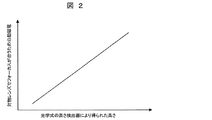
- the block diagram of a scanning electron microscope The graph which shows the relationship between the excitation current of a height detector and an objective lens.
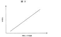
- the graph which shows the relationship between the temperature of an objective lens, and a working distance (WD).
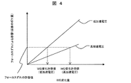
- the graph which shows that the allowable value of a working distance change changes with acceleration voltages.
- the conceptual diagram which replaces the allowable value of a working distance change with the allowable value of a temperature change.
- the graph which shows that the allowable value of a temperature change changes with acceleration voltages.
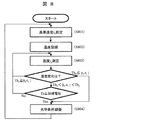
- the flowchart which shows the process of adjusting optical conditions with a different frequency according to measured temperature.
- the figure which shows the outline
- the flowchart which shows the process of adjusting optical conditions with a different frequency according to measured temperature.
- the flowchart which shows the process of adjusting optical conditions with a different frequency according to measured temperature.
- the scanning electron microscope is equipped with a magnetic field type objective lens for focusing and irradiating a sample with an electron beam emitted from an electron gun.
- the excitation current of the objective lens is increased or decreased in accordance with changes in observation conditions such as change in acceleration voltage and change in sample height. Heat is generated when an excitation current is passed through the objective lens.
- the excitation current increases or decreases due to changes in acceleration voltage or sample height, the heat generated from the objective lens changes.
- the acceleration voltage is low, the amount of heat generated is low and the temperature is low, and when the acceleration voltage is high, The calorific value is large and high.
- a working distance (WD) that is a distance between the objective lens and the sample changes.
- Focus adjustment is generally performed by autofocus, but it takes time and throughput decreases.
- a method is used in which the wafer surface height is detected by an optical height detector, a so-called Z sensor, and the focus is adjusted based on the surface height.
- the Z sensor it is necessary to adjust the relationship between the height information obtained by the Z sensor and the focal position of the objective lens in advance, but when the temperature of the objective lens changes and the WD changes, Since the relationship between the focal positions of the Z sensor and the objective lens changes, adjustment is necessary again.
- a charged particle beam apparatus that optimizes the frequency of correction such as focus adjustment during operation of the apparatus until the temperature monitored by the thermometer stabilizes or during a predetermined time. Specifically, when the acceleration voltage is changed from a high acceleration voltage to a low acceleration voltage and when the acceleration voltage is changed from a low acceleration voltage to a high acceleration voltage, the latter is more resistant to defocus due to a temperature change.
- a charged particle beam apparatus that sets an appropriate adjustment frequency in accordance with how the acceleration voltage is switched, such as setting the adjustment frequency lower than the former, will be described.
- FIG. 1 is a diagram illustrating an example of the configuration of a scanning electron microscope.
- the electrons generated from the electron source 101 are accelerated by the primary electron acceleration electrode 113 to which a voltage is applied from the primary electron acceleration power source 112 and then decelerated by the retarding voltage applied to the sample 107 from the retarding power source 110. Further, the light is focused by the objective lens 106 and irradiated onto the sample 107 on the sample stage 111.
- a height sensor 112 is provided in order to monitor the change in the surface height of the sample 107. Since the change in height affects the focus shift, the focal length is adjusted by changing the excitation intensity of the objective lens 106 so as to focus on the height of the surface of the sample 107 measured by the height sensor 112. .
- the control device 128 performs electrical control of each control unit shown below.
- the beam of the primary electron beam 102 is scanned on the sample by the deflection (scanning) coil 105, and the output of the secondary electron detector 109 is amplified by the amplifier 121 as an electric signal in synchronization with the scanning.
- the amplified electric signal is calculated by the calculation unit 122, converted into luminance information such as image density, and stored in the image memory 123 as a captured image.
- the stored image is displayed on the display device 125 after being acquired as a two-dimensional image of the shape of the sample surface or after being calculated by the calculation device 124 described later.
- image processing according to the purpose is performed by image processing hardware such as a CPU.
- the arithmetic device 124 also has a function of creating a line profile based on the luminance information of the image stored in the image memory 123 and measuring a dimension between peaks of the profile.
- a result obtained by the processing is displayed on a display device 125 such as an external display connected to the arithmetic device 124.
- the display device 125 has a function such as a GUI that displays an image, an inspection result, and the like to the operator.
- the control device 128 is an apparatus and network or path for creating an imaging recipe for creating an imaging recipe including the coordinates of an electronic device required for length measurement and inspection, a pattern matching template used for positioning, imaging conditions, and the like. Etc. can also be connected.
- the control device 128 naturally includes a control unit (not shown).
- each control unit included in the control device 128 may be implemented by hardware or software, and a plurality of control units may be implemented collectively according to device conditions.
- the height sensor 113 will be briefly described with reference to FIG.
- a method is used in which the wafer surface height is detected by an optical height detector and a Z sensor, and focusing is performed based on the surface height. This is because the relationship between the height obtained by the Z sensor and the excitation current focused by the objective lens is obtained in advance using samples having different heights, and the height obtained by the Z sensor is measured in the objective lens during actual measurement.
- the electron beam is focused at high speed.
- the excitation current of the objective lens When changing the acceleration voltage, it is necessary to change the excitation current of the objective lens. Generally, when the acceleration voltage is set high, the energy of primary electrons becomes strong. Therefore, in order to converge the electrons, the excitation current is increased and the magnetic field is strengthened. Conversely, when the acceleration voltage is set low, the excitation current is reduced and the magnetic field is weakened.
- the excitation current of the objective lens needs to be increased or decreased according to the acceleration voltage used in this way, but the amount of heat generated from the objective lens changes by increasing or decreasing the excitation current. That is, when the acceleration voltage is high, the temperature of the objective lens is high, and when the acceleration voltage is low, the temperature of the objective lens is low. When the temperature of the objective lens changes, the objective lens expands or contracts.
- the distance (WD) between the objective lens and the sample changes as the objective lens expands or contracts.
- the relationship between the height obtained by the Z sensor and the focal position of the objective lens changes. Therefore, even if the objective lens is used for focusing from the height obtained from the Z sensor, the focus is not achieved.
- FIG. 3 shows the relationship of the distance (WD) from the sample with respect to the temperature of the objective lens, and shows that WD changes when the temperature of the objective lens changes.
- the focus shift due to the change in WD differs depending on the acceleration voltage used.
- the influence of the focus shift is large at a low acceleration voltage, and the influence is small at a high acceleration voltage.
- the allowable value of the focus shift is constant regardless of the acceleration voltage, the allowable change amount of WD is small at the low acceleration voltage and large at the high acceleration voltage.
- the allowable WD change amount is converted into an allowable temperature change amount, as shown in FIG. 5, since the allowable value of the WD change is small at the low acceleration voltage, the allowable value of the temperature change is small, and the WD change is high at the high acceleration voltage. Since the allowable value of is large, the allowable value of the temperature change is also large.
- the sign changes, but the amount of change is the same.
- the amount of temperature change that occurs when the acceleration voltage is changed is the same, but when changing from a low acceleration voltage to a high acceleration voltage, it is more resistant to defocus due to temperature change, so the adjustment frequency is high acceleration.
- the voltage can be set lower than when changing from a voltage to a low acceleration voltage.
- FIG. 8 is a flowchart showing a process of determining the adjustment timing of the optical conditions.
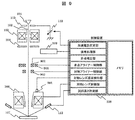
- FIG. 9 is a diagram for explaining the control device of the scanning electron microscope in more detail.
- the control device 128 controls an acceleration voltage setting unit that controls the acceleration voltage power source 112 and an astigmatism corrector 902, and performs an astigmatism correction unit that performs beam astigmatism correction, and the center of the astigmatism corrector 902 (ideal optical axis). ),
- An astigmatism controller for controlling the astigmatism aligner 905 for aligning the beam, an objective aligner control section for controlling the objective aligner 903 for aligning the beam at the center of the objective lens 106, and an objective lens.
- An objective lens temperature control unit that detects a temperature change of the objective lens using a thermometer 901 that measures the temperature of the objective lens, an objective lens control unit that controls the objective lens 106 based on the height measurement of the Z sensor, and a Z sensor ( A sample height measuring unit or the like for measuring the height of the sample surface using the height sensor 113) is included.
- the optical conditions are adjusted and the reference temperature t1 of the objective lens is measured (step 801).
- the objective lens condition which is one of the optical conditions. Since an appropriate condition changes according to the height of the sample, the height of the object is measured using the Z sensor, and the condition of the objective lens is set so that the measured height is in focus.
- the relationship between the measured value (sample height) of the Z sensor and the objective lens condition (excitation current) is stored in advance in a memory or the like in the control device as a table or a relational expression. Based on this information, objective lens control is performed.
- the unit controls the excitation current of the objective lens 106.
- thermometer 901 is directly attached to the objective lens 901 .
- the present invention is not limited to this, and any position suitable for identifying the shape change of the objective lens may be used.
- the position does not matter.
- the measured temperature t1 is stored in the memory (step 802).
- the temperature t2 is measured after obtaining the reference temperature t1 (step 803).
- the temperature of the objective lens is constantly monitored, and when a predetermined change appears in the temperature, control is performed as described later.
- temperature measurement is performed in predetermined time units. May be.
- the adjustment frequency of the optical condition is changed according to the apparatus condition, it is possible to suppress a decrease in throughput due to high-frequency adjustment, and further adjust the optical condition at an appropriate timing. Therefore, it is possible to keep the condition of the apparatus stable.
- the optical conditions may vary greatly, so the optical conditions are adjusted uniformly regardless of the acceleration voltage.
- the flowchart of FIG. 8 is one of “do not adjust the optical condition”, “select whether or not to adjust the optical condition according to the acceleration voltage”, and “adjust the optical condition” according to the temperature change.
- the present invention is not limited to this, and the adjustment frequency may be changed linearly according to the value of the acceleration voltage or the magnitude of the change in the acceleration voltage.
- the optical frequency adjustment frequency when changing from "low acceleration voltage to high acceleration voltage” should be less than the adjustment frequency when changing from "high acceleration voltage to low acceleration voltage”. It is possible to adjust the optical conditions at a frequent adjustment frequency.
- FIG. 10 is a flowchart showing a process of adjusting the adjustment frequency of the optical condition depending on whether the temperature of the objective lens is decreasing or increasing.
- the fact that the temperature is decreasing is a state after the excitation current of the objective lens is weakened, that is, after the acceleration voltage is changed from a high state to a low state. Increase the frequency of adjustment.
- the temperature rise means that the excitation current of the objective lens is intensified, that is, the state after the state after the acceleration voltage is changed from a low state to a high state, so that it is relatively adjusted. Reduce frequency.
- the optical conditions can be adjusted with an appropriate adjustment frequency by such a determination process.
- FIG. 11 is a flowchart showing still another optical condition adjustment frequency determination step.
- An acceleration voltage is set according to the sample to be measured (S01). After the acceleration voltage is set, the electron beam axis adjustment and the relationship between the height obtained by the Z sensor and the focal position of the objective lens are adjusted (S02). At this time, the temperature of the objective lens unit is stored together (S02). Pattern dimensions and the like are measured by recipe processing (S03). During the processing of the recipe, the temperature of the objective lens is periodically measured (S04) and compared with the temperature recorded in S02 (S06). If there is a temperature change, an inquiry is made about the acceleration voltage currently in use (S06). If the allowable temperature change is exceeded, the electron beam axis adjustment and the height obtained by the Z sensor and the focal position of the objective lens Are adjusted (S02).
- the adjustment frequency of the optical condition when changing from “low acceleration voltage to high acceleration voltage” is set to “high acceleration voltage to low acceleration voltage”. Less than the adjustment frequency when changing to.
- Example 2 In Example 1, the temperature of the objective lens was measured periodically, and an allowable value for temperature change was set for each acceleration voltage, and the adjustment frequency was optimized, but the amount of temperature change when the acceleration voltage was changed was experimental. If the knowledge is obtained by the above, the frequency of adjustment can be optimized from the acceleration voltage used and the allowable temperature change with respect to the acceleration voltage in FIG. 6 without measuring the temperature.
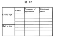
- the type of change in acceleration voltage (change from low acceleration voltage to high acceleration voltage (Low to High), or change from high acceleration voltage to low acceleration voltage (High to Low)).
- different adjustment frequencies may be stored as a table in advance, and the adjustment frequency may be read based on the acceleration voltage setting to set the apparatus.
- the adjustment frequency stored in “Low to High” is set relatively low compared to the adjustment frequency stored in “High to Low”.
- an arithmetic expression for calculating the difference ( ⁇ Vacc) between the acceleration voltages before and after adjusting the acceleration voltage is stored in the control device 128, and the adjustment frequency is automatically set according to the setting of the acceleration voltage. good.
- FIG. 12 shows an example in which a different adjustment frequency (Frequency of adjustment) and an adjustment period (Adjustment Period) based on the data stored in this table are stored according to the magnitude of ⁇ Vacc.
- the method of the present embodiment it is possible to select an appropriate adjustment frequency that changes depending on the temperature change condition without performing temperature measurement, and further, adjustment is performed based on a predetermined database. It is also possible to accurately manage the operation time.
- Example 3 In the first embodiment, an example has been given regarding the focus shift caused by the temperature change of the objective lens. Similarly, the electron beam axis shift and the astigmatism shift caused by the temperature change of the objective lens are similarly performed. Adjustment frequency can be optimized. In this case, the adjustment frequency using the objective aligner 903 and the astigmatism corrector 902 is set as in the first and second embodiments.
- Example 4 In the third embodiment, an example has been given regarding the deviation of the electron beam axis and the astigmatism caused by the temperature change of the objective lens. Similarly, the electron beam axis deviation caused by the temperature change of the condenser lens and the astigmatism corrector. Regarding the axis deviation with respect to 902, the temperature of the condenser lens unit is monitored and the allowable temperature change amount is obtained, whereby the axis adjustment frequency of the electron beam can be optimized. In this case, the adjustment frequency using the astigmatism aligner 905 or the like is set as in the first embodiment or the second embodiment.
- Electron Source 102 Primary Electron Beam 103 Condenser Lens 104 Reflector 105 Deflection (Scanning) Coil 106 Objective Lens 107 Wafer (Sample) 108 Secondary Electron 109 Secondary Electron Detector 110 Retarding Power Supply 111 Sample Stage 112 Acceleration Power Supply 113 Height Sensor 121 Amplifier 122 Operation Unit 123 Image Memory 124 Operation Device 125 Display Device 128 Control Device
Landscapes
- Chemical & Material Sciences (AREA)
- Analytical Chemistry (AREA)
- Electron Sources, Ion Sources (AREA)
Abstract
本発明の荷電粒子線装置は、荷電粒子源(101)と、加速電極(113)と、一次荷電粒子線(102)を調整する光学素子(106,902,903,905)と、対物レンズ(106)の温度変化を測定する温度計(901)と、前記加速電極及び前記光学素子を制御する制御装置(128)を備える。 前記制御装置は、(ア)一次荷電粒子線の加速電圧が所定の値より高い場合は、第1の温度変化を検出したときに、(イ)一次荷電粒子線の加速電圧が所定の値以下の場合は前記第1の温度変化より小さな第2の温度変化を検出したときに、光学素子の調整を行う。 これにより、一次荷電粒子線の加速電圧を変化させたときの光学条件への影響の抑制と、装置の高スループット化の両立を実現できる。
Description
本発明は荷電粒子線装置に係り、特に温度変化による光学条件への影響を効果的に抑制し得る荷電粒子線装置に関する。
半導体デバイス等を測定、検査する走査電子顕微鏡に代表される荷電粒子線装置では、測定等の対象となる試料を装置内に搬入した後、測定する試料に応じ最適な光学条件に設定し試料の測定を行う。これは電子線を照射によりパターンが収縮するような電子線に耐性のない試料には加速電圧を低く設定する必要があり、一方、アスペクト比の高いホールなどの試料を測定するには高い加速電圧を設定する必要があるためである。
特許文献1には、設定された加速電圧に応じて対物レンズの励磁電流を設定すると共に、当該励磁電流の変化に応じて対物レンズの温度調整を、冷却水を用いて行う走査電子顕微鏡が開示されている。
特許文献1に開示の手法によれば、加速電圧の変化に応じて、対物レンズの温度を制御することができるが、実際には冷却水を用いて、温度が変化する部分を選択的に、且つ精密に温度調整することは困難である。高精度なフォーカス条件を長時間に亘って維持するためには、その温度変化に応じて対物レンズのレンズ条件を制御する必要がある。しかしながら、対物レンズの励磁状態を適正化するために、高頻度でフォーカス調整を行うと、光学条件調整に時間がかかり、装置のスループットが低下する。
以下に、ビームの加速電圧を変化させたときの光学条件への影響の抑制と、装置の高スループット化の両立を目的とする荷電粒子線装置について説明する。
上記目的を達成するための一態様として、荷電粒子源と、当該荷電粒子源から放出される荷電粒子を加速する加速電極と、当該加速電極によって加速された荷電粒子線を調整する光学素子と、当該加速電極及び光学素子を制御する制御装置を備えた荷電粒子線装置において、当該制御装置は、所定の加速電圧より高い加速電圧が設定されている場合には、第1の温度変化を検出したときに、前記光学素子の調整を行い、所定の加速電圧以下の加速電圧が設定されている場合には、前記第1の温度変化より小さな第2の温度変化を検出したときに、前記光学素子の調整を行う荷電粒子線装置を提案する。
また、上記目的を達成するための他の一態様として、上記制御装置が、前記加速電圧に印加する電圧を高電圧から低電圧に変化させたときと比較して、低電圧から高電圧に変化させたときに、前記光学素子による前記荷電粒子線の光学条件の調整頻度を少なくするように、前記光学素子を制御する荷電粒子線装置を提案する。
上記構成によれば、ビームの加速電圧を変化させたときの光学条件への影響の抑制と、装置の高スループット化の両立が可能となる。
走査電子顕微鏡は電子銃から放出された電子線を試料に焦点合わせして照射するために磁界型対物レンズが備えられている。対物レンズの励磁電流は、加速電圧の変更や試料高さの変更など、観察条件の変更に合わせて増減される。対物レンズに励磁電流を流すと熱が発生する。加速電圧の変更や試料高さの変更などで励磁電流が増減すると、対物レンズから発生する熱は変化し、一般的に加速電圧が低い場合、発熱量は少なく低温となり、加速電圧が高い場合、発熱量は大きく高温となる。
対物レンズの温度が変化すると、対物レンズが膨張あるいは収縮する。対物レンズが膨張あるいは収縮することで対物レンズと試料との距離であるワーキングディスタンス(WD)が変化する。
一般的にフォーカス調整はオートフォーカスにより行われるが、時間がかかりスループットが低下する。フォーカス調整に必要な時間を短縮するため、ウェハ表面高さを光学式の高さ検出器、いわゆるZセンサで検出し、その表面高さを元にフォーカスを合わせる方式が用いられる。Zセンサによってフォーカスをあわせるには、あらかじめZセンサにより得られる高さ情報と対物レンズでの焦点位置の関係を調整しておく必要があるが、対物レンズの温度が変化し、WDが変化すると、Zセンサと対物レンズでの焦点位置の関係が変化するため再び調整が必要になる。
加速電圧の変更により対物レンズの温度が変化し、温度が安定するまでには長時間を要する。そのため、温度が安定するまでは定期的に調整が必要となり、スループットが低下する。
以下に説明する実施例では、例えば装置の稼動中、温度計によりモニタした温度が安定するまで、あるいは所定時間中、フォーカス調整などの補正頻度を適正化する荷電粒子線装置を説明する。具体的には、加速電圧を高加速電圧から低加速電圧に変化させる場合と、低加速電圧から高加速電圧に変化させる場合とでは、後者の方が温度変化に伴うフォーカスずれに対する耐性があるため、調整頻度は前者よりも少なく設定するなど、加速電圧の切り替え方に応じた適切な調整頻度を設定する荷電粒子線装置を説明する。
上記構成によれば、光学条件の調整状態の維持と、調整頻度の適正化によるスループット低下の抑制の両立を実現できる。特に加速電圧変更時の調整頻度の適正化を実現することが可能となる。
(実施例1)
図1は、走査電子顕微鏡の構成の1例を示す図である。電子源101から発生した電子は、一次電子加速電源112から電圧が印加された一次電子加速電極113によって加速されたのちに、リターディング電源110から試料107に印加されたリターディング電圧により減速され、かつ対物レンズ106により集束されて試料ステージ111上の試料107上に照射される。試料107に一次電子線102が照射されると、試料107から二次電子108が発生し、二次電子108はリターディング電圧によって形成される電界により電子源側に加速される。二次電子108は反射板104にあたり、反射板104で発生した二次電子108が二次電子検出器109で捕捉され、二次電子検出器109に入射する電子の量に応じて二次電子検出器109の出力が変化する。
(実施例1)
図1は、走査電子顕微鏡の構成の1例を示す図である。電子源101から発生した電子は、一次電子加速電源112から電圧が印加された一次電子加速電極113によって加速されたのちに、リターディング電源110から試料107に印加されたリターディング電圧により減速され、かつ対物レンズ106により集束されて試料ステージ111上の試料107上に照射される。試料107に一次電子線102が照射されると、試料107から二次電子108が発生し、二次電子108はリターディング電圧によって形成される電界により電子源側に加速される。二次電子108は反射板104にあたり、反射板104で発生した二次電子108が二次電子検出器109で捕捉され、二次電子検出器109に入射する電子の量に応じて二次電子検出器109の出力が変化する。
試料107の表面高さの変化をモニタリングするために、高さセンサ112が設けられている。高さの変化は、焦点のずれに影響するため、高さセンサ112で計測された試料107の表面の高さに焦点を合わせるように、対物レンズ106の励磁強度を変えて焦点距離を調整する。
制御装置128は、以下に示す各制御部の電気的制御を行う。一次電子線102のビームは、偏向(走査)コイル105により試料上にて走査され、走査に同期して二次電子検出器109の出力が電気信号として増幅器121で増幅される。増幅された電気信号は演算部122によって演算され、画像の濃淡などの輝度情報に変換されて撮像画像として画像メモリ123に格納される。格納された画像は、試料表面の形状の二次元画像として取得されたのち、もしくは後述する演算装置124にて演算されたのち、表示装置125に表示される。
演算装置124では、CPU等の画像処理ハードウェアによって、目的に応じた画像処理が行われる。また、演算装置124は、画像メモリ123に格納された画像の輝度情報に基づいて、ラインプロファイルを作成し、プロファイルのピーク間の寸法を測定する機能をも備えている。当該処理により得られた結果は、演算装置124に接続された外部ディスプレイ等の表示装置125に表示される。表示装置125には、操作者に対して画像や検査結果等を表示するGUI等の機能を有する。
制御装置128は、測長や検査等に必要とされる電子デバイスの座標、位置決めに利用するパターンマッチング用のテンプレート、撮影条件等を含む撮像レシピを作成する撮像レシピを作成する装置とネットワークまたはパス等を介して接続することもできる。また、制御装置128には、当然のことながら図示しない制御部も含まれている。また、制御装置128に含まれる各制御部はハード実装されてもソフト実装されてもよく、装置条件に応じて複数の制御部がまとめて実装されていてもよい。
高さセンサ113に関して図2を使用して簡単に説明する。走査電子顕微鏡による検査、測定位置でのフォーカス合わせはウェハ表面高さを光学式の高さ検出器、Zセンサで検出し、その表面高さを元にフォーカスを合わせる方式が用いられる。これは、あらかじめ高さの異なる試料を使用してZセンサにより得られる高さと対物レンズで焦点が合う励磁電流の関係を求めておき、実際の測定時にはZセンサにより得られた高さを対物レンズの電流値に変換し、電子線のフォーカスを高速に合わせる方式である。
加速電圧を変更した場合、対物レンズの励磁電流を変更する必要がある。一般的に加速電圧を高く設定すると、1次電子のエネルギーが強くなるため、電子を収束させるには励磁電流を増やし磁界を強くする。反対に加速電圧を低く設定する場合は励磁電流を減らし磁界を弱くする。このように使用する加速電圧に応じて、対物レンズの励磁電流は増減する必要があるが、励磁電流を増減することで対物レンズからの発熱量が変化する。つまり、加速電圧が高い場合は対物レンズの温度は高く、加速電圧が低い場合は対物レンズの温度は低くなる。対物レンズの温度が変化すると、対物レンズが膨張あるいは収縮する。対物レンズが膨張あるいは収縮することで対物レンズと試料との距離(WD)が変化する。WDが変化すると、Zセンサにより得られる高さと対物レンズでの焦点位置の関係が変わるため、Zセンサから求めた高さから、対物レンズでフォーカスを合わせてもフォーカスは合わない。Zセンサによりフォーカスが合うようにするには再度、Zセンサにより得られる高さと対物レンズでの焦点位置の関係を調整する必要があるが、対物レンズの温度は安定するまでに数時間を要するため、その間は定期的に調整を行う必要がある。
図3は対物レンズの温度に対する試料との距離(WD)の関係を示しており、対物レンズの温度が変化するとWDが変化することを示している。WDが変わるとZセンサで検出する高さとの相関が変化し、フォーカスがずれる。
WDの変化によるフォーカスのずれは図4に示すとおり、使用する加速電圧により異なり、一般的に低加速電圧ではフォーカスずれによる影響は大きく、高加速電圧では影響は少なくなる。つまりフォーカスずれの許容値は加速電圧によらず一定であるため、許容できるWDの変化量は低加速電圧では少なく、高加速電圧では大きくなる。
許容できるWDの変化量を許容できる温度変化量に換算すると、図5に示すように、低加速電圧ではWD変化の許容値が少ないため、温度変化の許容値も少なく、高加速電圧ではWD変化の許容値が大きいため、温度変化の許容値も大きくなる。
加速電圧と温度変化の許容値の関係を求めると図6のような関係が得られ、使用する加速電圧により、許容できる温度変化量は異なる。
一方、図7に示すとおり、加速電圧を低加速電圧から高加速電圧に切り替えたときに変化する温度Δt1と、高加速電圧から低加速電圧に切り替えたときに変化する温度Δt2はΔt1=-Δt2の関係が成り立ち、符号が変転するが変化量は同じである。
つまり、加速電圧を変更した際に生じる温度変化量は同じであるが、低加速電圧から高加速電圧に変化させる場合の方が温度変化に伴うフォーカスずれに対する耐性があるため、調整頻度は高加速電圧から低加速電圧に変化させる場合よりも低く設定することができる。このように加速電圧の切り替え方に応じて適切な調整頻度を設定することにより、スループットの低下を防ぐことができる。
図8は光学条件の調整タイミングを決定する工程を示すフローチャートである。図9は走査電子顕微鏡の制御装置をより詳細に説明する図である。制御装置128には、加速電圧電源112を制御する加速電圧設定部、非点補正器902を制御し、ビームの非点補正を行う非点補正部、非点補正器902の中心(理想光軸)にビームの軸合わせを行うための非点アライナー905を制御する非点アライナー制御部、対物レンズ106の中心にビームの軸合わせを行うための対物アライナー903を制御する対物アライナー制御部、対物レンズの温度を測定する温度計901を用いて対物レンズの温度変化を検出する対物レンズ温度制御部、Zセンサの高さ測定に基づいて、対物レンズ106を制御する対物レンズ制御部、及びZセンサ(高さセンサ113)を用いて試料面の高さ測定を行う試料高さ計測部等が含まれている。
まず、ある加速電圧から、他の加速電圧に切り換えたときに、光学条件を調整し、対物レンズの基準温度t1を計測する(ステップ801)。光学条件の1つである対物レンズ条件は。試料の高さに応じて適正な条件が変化するため、Zセンサを用いて高さ計測を行い、当該計測された高さに焦点が合うように、対物レンズの条件を設定する。Zセンサの計測値(試料高さ)と対物レンズ条件(励磁電流)との関係は予め制御装置内のメモリ等に、テーブル、或いは関係式として記憶されており、この情報に基づいて対物レンズ制御部は対物レンズ106の励磁電流を制御する。なお、本実施例では温度計901が対物レンズ901に直に取り付けられている例を説明するが、これに限られることはなく、対物レンズの形状変化を同定するのに好適な位置であればその位置は問わない。測定された温度t1はメモリに記憶される(ステップ802)。
次に、対物レンズの温度変化を同定するために、基準温度t1の取得後に温度t2を測定する(ステップ803)。本実施例では、対物レンズの温度を常時モニタし、当該温度に所定の変化が現れた場合に、後述するような制御を行う例について説明するが、所定の時間単位で温度計測を行うようにしても良い。
以上のようにして計測された温度から求められる|t2-t1|が第1の閾値Th1である場合には、大きな温度変化がなく、対物レンズの変形量も許容できる範囲であるため、温度計測を継続する。一方、|t2-t1|が第1の閾値Th1より大きく、第2の閾値Th2より小さい場合には、そのときに設定されている加速電圧の大きさによって、その後の処理を変化させる。加速電圧が所定の閾値より大きい場合は、上述したように温度変化に対する耐性があるため、スループットを優先して光学条件を調整することなく、現状の光学条件を維持する。一方、加速電圧が所定値以下の場合、上述のように温度変化によるフォーカスずれの影響が顕著に発生するため、装置条件の適正化を優先して、光学条件の調整を行う(ステップ804)。
このように、装置条件に応じて光学条件の調整頻度を変化させているため、高頻度で調整を行うことによるスループットの低下を抑制することができ、更に適正なタイミングで光学条件を調整することになるため、装置のコンディションを安定に保つことが可能となる。
なお、温度変化が第2の閾値Th2を越えた場合には、光学条件が大きく変動している可能性があるため、加速電圧に関らず一様に光学条件を調整する。図8のフローチャートは、温度変化に応じて、「光学条件を調整しない」、「加速電圧に応じて光学条件を調整するか否か選択する」、及び「光学条件を調整する」の内の1つを選択する例を説明したものであるが、これに限られることはなく、加速電圧の値や加速電圧の変化の大きさに応じて、調整頻度をリニアに変化させるようにしても良い。結果として「低加速電圧から高加速電圧」に変化させたときの光学条件の調整頻度を、「高加速電圧から低加速電圧」に変化させたときの調整頻度より少なくするようにすれば、適正な調整頻度で光学条件の調整を行うことができる。
図10は、対物レンズの温度が下降しているのか、上昇しているのかによって、光学条件の調整頻度を調整する工程を示すフローチャートである。温度が下降しているということは、対物レンズの励磁電流を弱めている、即ち加速電圧を高い状態から低い状態に変化させた後の状態であるため、逆の場合と比較して相対的に調整頻度を増加させる。一方、温度が上昇しているということは、対物レンズの励磁電流を強めている、即ち加速電圧を低い状態から高い状態に変化させた状態の後で後の状態であるため、相対的に調整頻度を減少させる。このような判断工程によっても適正な調整頻度で光学条件の調整を行うことができる。
図11は、更に他の光学条件調整頻度決定工程を示すフローチャートである。測定する試料に応じて加速電圧を設定する(S01)。加速電圧の設定後、電子線の軸調整およびZセンサにより得られる高さと対物レンズでの焦点位置の関係を調整する(S02)。このとき対物レンズ部の温度を合わせて記憶する(S02)。レシピ処理によりパターン寸法などの測定を行う(S03)。レシピの処理中は定期的に対物レンズの温度を測定し(S04)、S02で記録した温度との比較を行う(S06)。温度変化がある場合、現在使用中の加速電圧の問い合わせを行い(S06)、許容温度変化量を超えている場合は、電子線の軸調整およびZセンサにより得られる高さと対物レンズでの焦点位置の関係を調整する(S02)。
この場合、加速電圧に応じて異なる許容量を設定しておき、結果として「低加速電圧から高加速電圧」に変化させたときの光学条件の調整頻度を、「高加速電圧から低加速電圧」に変化させたときの調整頻度より少なくする。
許容温度変化量に達していない場合は測長などの処理を行う(S08)。これらをレシピ処理が終了するまで繰り返し行う。
(実施例2)
実施例1では定期的に対物レンズの温度を測定し、加速電圧ごとに温度変化の許容値を設け、調整頻度の最適化を行ったが、加速電圧を変化させたときの温度変化量が実験などで知見が得られているのであれば、温度を測定しなくても、使用している加速電圧と図6の加速電圧に対する許容温度変化量から調整の頻度を最適化することができる。
(実施例2)
実施例1では定期的に対物レンズの温度を測定し、加速電圧ごとに温度変化の許容値を設け、調整頻度の最適化を行ったが、加速電圧を変化させたときの温度変化量が実験などで知見が得られているのであれば、温度を測定しなくても、使用している加速電圧と図6の加速電圧に対する許容温度変化量から調整の頻度を最適化することができる。
例えば図12に例示するように、加速電圧の変化の種類(低加速電圧から高加速電圧への変化(Low to High)、或いは高加速電圧から低加速電圧への変化(High to Low))に応じて、異なる調整頻度を予めテーブルとして記憶しておき、加速電圧の設定に基づいて、調整頻度を読み出して、装置の設定を行うようにすると良い。図12に例示するテーブルでは、“Low to High”に記憶された調整頻度は、“High to Low”に記憶された調整頻度に比べて相対的に、低頻度に設定されている。
また、制御装置128に加速電圧の調整前後の加速電圧の差分(ΔVacc)を演算する演算式を記憶させておき、加速電圧の設定に応じて、自動的に調整頻度を設定するようにしても良い。
図12の例では、ΔVaccの大きさに応じて、異なる調整頻度(Frequency of adjustment)とこのテーブルに記憶されたデータに基づく調整期間(Adjustment Period)が記憶されている例を示している。
本実施例の手法によれば、温度計測を行わなくても、温度変化条件によって変化する適正な調整頻度を選択することが可能となり、更に、所定のデータベースに基づいて調整を行うため、装置の稼働時間を正確に管理することも可能となる。
(実施例3)
実施例1では対物レンズの温度変化により発生するフォーカスずれに関して例をあげたが、同様に対物レンズの温度変化により発生する電子線の軸ずれ、非点収差のずれに関しても同様に電子線の軸調整頻度の最適化を行うことができる。この場合、対物アライナー903や非点補正器902を用いた調整頻度を、実施例1や実施例2のように設定する。
(実施例4)
実施例3では対物レンズの温度変化により発生する電子線の軸ずれ、非点収差のずれに関して例をあげたが、同様にコンデンサレンズの温度変化により発生する電子線の軸ずれ、非点補正器902に対する軸ずれに関しても、コンデンサレンズ部の温度をモニタし、許容温度変化量を求めることで、電子線の軸調整頻度の最適化を行うことができる。この場合、非点アライナー905等を用いた調整頻度を、実施例1や実施例2のように設定する。
(実施例3)
実施例1では対物レンズの温度変化により発生するフォーカスずれに関して例をあげたが、同様に対物レンズの温度変化により発生する電子線の軸ずれ、非点収差のずれに関しても同様に電子線の軸調整頻度の最適化を行うことができる。この場合、対物アライナー903や非点補正器902を用いた調整頻度を、実施例1や実施例2のように設定する。
(実施例4)
実施例3では対物レンズの温度変化により発生する電子線の軸ずれ、非点収差のずれに関して例をあげたが、同様にコンデンサレンズの温度変化により発生する電子線の軸ずれ、非点補正器902に対する軸ずれに関しても、コンデンサレンズ部の温度をモニタし、許容温度変化量を求めることで、電子線の軸調整頻度の最適化を行うことができる。この場合、非点アライナー905等を用いた調整頻度を、実施例1や実施例2のように設定する。
101 電子源
102 一次電子線
103 コンデンサレンズ
104 反射板
105 偏向(走査)コイル
106 対物レンズ
107 ウェハ(試料)
108 二次電子
109 二次電子検出器
110 リターディング電源
111 試料ステージ
112 加速電源
113 高さセンサ
121 増幅器
122 演算部
123 画像メモリ
124 演算装置
125 表示装置
128 制御装置
102 一次電子線
103 コンデンサレンズ
104 反射板
105 偏向(走査)コイル
106 対物レンズ
107 ウェハ(試料)
108 二次電子
109 二次電子検出器
110 リターディング電源
111 試料ステージ
112 加速電源
113 高さセンサ
121 増幅器
122 演算部
123 画像メモリ
124 演算装置
125 表示装置
128 制御装置
Claims (11)
- 荷電粒子源と、当該荷電粒子源から放出される荷電粒子を加速する加速電極と、当該加速電極によって加速された荷電粒子線を調整する光学素子と、当該加速電極及び光学素子を制御する制御装置を備えた荷電粒子線装置において、
当該制御装置は、所定の加速電圧より高い加速電圧が設定されている場合には、第1の温度変化を検出したときに、前記光学素子の調整を行い、所定の加速電圧以下の加速電圧が設定されている場合には、前記第1の温度変化より小さな第2の温度変化を検出したときに、前記光学素子の調整を行うことを特徴とする荷電粒子線装置。 - 請求項1において、
前記制御装置は、設定される加速電圧に応じて異なる調整頻度で上記光学素子の調整を行うことを特徴とする荷電粒子線装置。 - 請求項1において、
前記光学素子は対物レンズであることを特徴とする荷電粒子線装置。 - 請求項3において、
前記荷電粒子線が照射される試料の高さを計測する高さ計測装置を備え、前記制御装置は、前記加速電圧に応じて異なる頻度で、前記試料高さ計測に応じて、前記対物レンズの調整を行うことを特徴とする荷電粒子線装置。 - 請求項1において、
前記光学素子は、非点補正器であることを特徴とする荷電粒子線装置。 - 請求項1において、
前記光学素子は、光軸調整用のアライナーであることを特徴とする荷電粒子線装置。 - 荷電粒子源と、当該荷電粒子源から放出される荷電粒子を加速する加速電極と、当該加速電極によって加速された荷電粒子線を調整する光学素子と、当該加速電極及び光学素子を制御する制御装置を備えた荷電粒子線装置において、
前記制御装置は、前記加速電圧に印加する電圧を高電圧から低電圧に変化させたときと比較して、低電圧から高電圧に変化させたときに、前記光学素子による前記荷電粒子線の光学条件の調整頻度を少なくするように、前記光学素子を制御することを特徴とする荷電粒子線装置。 - 請求項7において、
前記光学素子は対物レンズであることを特徴とする荷電粒子線装置。 - 請求項8において、
前記荷電粒子線が照射される試料の高さを計測する高さ計測装置を備え、前記制御装置は、前記加速電圧に応じて異なる頻度で、前記試料高さ計測に応じて、前記対物レンズの調整を行うことを特徴とする荷電粒子線装置。 - 請求項7において、
前記光学素子は、非点補正器であることを特徴とする荷電粒子線装置。 - 請求項7において、
前記光学素子は、光軸調整用のアライナーであることを特徴とする荷電粒子線装置。
Applications Claiming Priority (2)
| Application Number | Priority Date | Filing Date | Title |
|---|---|---|---|
| JP2012-040858 | 2012-02-28 | ||
| JP2012040858A JP2013178876A (ja) | 2012-02-28 | 2012-02-28 | 荷電粒子線装置 |
Publications (1)
| Publication Number | Publication Date |
|---|---|
| WO2013129124A1 true WO2013129124A1 (ja) | 2013-09-06 |
Family
ID=49082326
Family Applications (1)
| Application Number | Title | Priority Date | Filing Date |
|---|---|---|---|
| PCT/JP2013/053607 Ceased WO2013129124A1 (ja) | 2012-02-28 | 2013-02-15 | 荷電粒子線装置 |
Country Status (2)
| Country | Link |
|---|---|
| JP (1) | JP2013178876A (ja) |
| WO (1) | WO2013129124A1 (ja) |
Families Citing this family (1)
| Publication number | Priority date | Publication date | Assignee | Title |
|---|---|---|---|---|
| JP6596295B2 (ja) | 2015-10-15 | 2019-10-23 | 株式会社日立ハイテクノロジーズ | 荷電粒子線装置 |
Citations (8)
| Publication number | Priority date | Publication date | Assignee | Title |
|---|---|---|---|---|
| JPS63200450A (ja) * | 1987-02-17 | 1988-08-18 | Nippon Telegr & Teleph Corp <Ntt> | 荷電ビ−ムの自動制御装置 |
| JPH0582067A (ja) * | 1991-09-20 | 1993-04-02 | Jeol Ltd | 対物レンズの励磁電流発生方式 |
| JPH05190132A (ja) * | 1992-01-13 | 1993-07-30 | Toshiba Corp | 走査型電子顕微鏡の自動焦点合わせ方法 |
| JPH1027563A (ja) * | 1996-07-10 | 1998-01-27 | Jeol Ltd | 走査電子顕微鏡 |
| JP2001084935A (ja) * | 1999-09-17 | 2001-03-30 | Hitachi Ltd | 電子顕微鏡 |
| JP2005038853A (ja) * | 2003-07-14 | 2005-02-10 | Fei Co | 二重ビーム装置 |
| JP2009134990A (ja) * | 2007-11-30 | 2009-06-18 | Jeol Ltd | 電子レンズ |
| JP2009176542A (ja) * | 2008-01-23 | 2009-08-06 | Horon:Kk | 電磁レンズ |
-
2012
- 2012-02-28 JP JP2012040858A patent/JP2013178876A/ja active Pending
-
2013
- 2013-02-15 WO PCT/JP2013/053607 patent/WO2013129124A1/ja not_active Ceased
Patent Citations (8)
| Publication number | Priority date | Publication date | Assignee | Title |
|---|---|---|---|---|
| JPS63200450A (ja) * | 1987-02-17 | 1988-08-18 | Nippon Telegr & Teleph Corp <Ntt> | 荷電ビ−ムの自動制御装置 |
| JPH0582067A (ja) * | 1991-09-20 | 1993-04-02 | Jeol Ltd | 対物レンズの励磁電流発生方式 |
| JPH05190132A (ja) * | 1992-01-13 | 1993-07-30 | Toshiba Corp | 走査型電子顕微鏡の自動焦点合わせ方法 |
| JPH1027563A (ja) * | 1996-07-10 | 1998-01-27 | Jeol Ltd | 走査電子顕微鏡 |
| JP2001084935A (ja) * | 1999-09-17 | 2001-03-30 | Hitachi Ltd | 電子顕微鏡 |
| JP2005038853A (ja) * | 2003-07-14 | 2005-02-10 | Fei Co | 二重ビーム装置 |
| JP2009134990A (ja) * | 2007-11-30 | 2009-06-18 | Jeol Ltd | 電子レンズ |
| JP2009176542A (ja) * | 2008-01-23 | 2009-08-06 | Horon:Kk | 電磁レンズ |
Also Published As
| Publication number | Publication date |
|---|---|
| JP2013178876A (ja) | 2013-09-09 |
Similar Documents
| Publication | Publication Date | Title |
|---|---|---|
| JP4644617B2 (ja) | 荷電粒子線装置 | |
| JP5075431B2 (ja) | 帯電測定方法、焦点調整方法、及び走査電子顕微鏡 | |
| US9324540B2 (en) | Charged particle beam device | |
| US6545275B1 (en) | Beam evaluation | |
| TWI792070B (zh) | 判定帶電粒子束工具所獲得之影像中之像差的方法、判定帶電粒子束工具之設置的方法、及帶電粒子束工具 | |
| US10340115B2 (en) | Charged particle beam apparatus | |
| JP2010087070A (ja) | 走査電子顕微鏡に用いられるレシピの診断装置 | |
| US10930468B2 (en) | Charged particle beam apparatus using focus evaluation values for pattern length measurement | |
| JP4194526B2 (ja) | 荷電粒子線の調整方法、及び荷電粒子線装置 | |
| JP5798099B2 (ja) | 画質調整方法、プログラムおよび電子顕微鏡 | |
| JP6310864B2 (ja) | 検査装置 | |
| WO2013129124A1 (ja) | 荷電粒子線装置 | |
| JP2010182424A (ja) | 荷電粒子線の光軸調整方法、及び荷電粒子線装置 | |
| US11276548B2 (en) | Charged particle beam device and charged particle beam adjustment method | |
| JP5470194B2 (ja) | 荷電粒子線装置 | |
| JP6230831B2 (ja) | 荷電粒子線装置および画像取得方法 | |
| US11557457B2 (en) | Charged particle beam apparatus | |
| JP2010182423A (ja) | 荷電粒子ビームの焦点評価方法及び荷電粒子線装置 | |
| JP4231891B2 (ja) | 荷電粒子線の調整方法、及び荷電粒子線装置 | |
| KR20080090118A (ko) | 반도체 검사 장치의 제어 방법 | |
| JP2006100049A (ja) | 電子線式検査装置とその検査方法 |
Legal Events
| Date | Code | Title | Description |
|---|---|---|---|
| 121 | Ep: the epo has been informed by wipo that ep was designated in this application |
Ref document number: 13754787 Country of ref document: EP Kind code of ref document: A1 |
|
| NENP | Non-entry into the national phase |
Ref country code: DE |
|
| 122 | Ep: pct application non-entry in european phase |
Ref document number: 13754787 Country of ref document: EP Kind code of ref document: A1 |