WO2013128581A1 - 撮像装置、撮像システム、撮像装置の駆動方法 - Google Patents
撮像装置、撮像システム、撮像装置の駆動方法 Download PDFInfo
- Publication number
- WO2013128581A1 WO2013128581A1 PCT/JP2012/054978 JP2012054978W WO2013128581A1 WO 2013128581 A1 WO2013128581 A1 WO 2013128581A1 JP 2012054978 W JP2012054978 W JP 2012054978W WO 2013128581 A1 WO2013128581 A1 WO 2013128581A1
- Authority
- WO
- WIPO (PCT)
- Prior art keywords
- signal
- digital
- pixel
- analog
- photoelectric conversion
- Prior art date
- Legal status (The legal status is an assumption and is not a legal conclusion. Google has not performed a legal analysis and makes no representation as to the accuracy of the status listed.)
- Ceased
Links
Images










Classifications
-
- H—ELECTRICITY
- H04—ELECTRIC COMMUNICATION TECHNIQUE
- H04N—PICTORIAL COMMUNICATION, e.g. TELEVISION
- H04N25/00—Circuitry of solid-state image sensors [SSIS]; Control thereof
- H04N25/60—Noise processing, e.g. detecting, correcting, reducing or removing noise
-
- H—ELECTRICITY
- H04—ELECTRIC COMMUNICATION TECHNIQUE
- H04N—PICTORIAL COMMUNICATION, e.g. TELEVISION
- H04N25/00—Circuitry of solid-state image sensors [SSIS]; Control thereof
- H04N25/70—SSIS architectures; Circuits associated therewith
- H04N25/76—Addressed sensors, e.g. MOS or CMOS sensors
- H04N25/77—Pixel circuitry, e.g. memories, A/D converters, pixel amplifiers, shared circuits or shared components
- H04N25/778—Pixel circuitry, e.g. memories, A/D converters, pixel amplifiers, shared circuits or shared components comprising amplifiers shared between a plurality of pixels, i.e. at least one part of the amplifier must be on the sensor array itself
-
- H—ELECTRICITY
- H04—ELECTRIC COMMUNICATION TECHNIQUE
- H04N—PICTORIAL COMMUNICATION, e.g. TELEVISION
- H04N25/00—Circuitry of solid-state image sensors [SSIS]; Control thereof
- H04N25/70—SSIS architectures; Circuits associated therewith
- H04N25/76—Addressed sensors, e.g. MOS or CMOS sensors
- H04N25/78—Readout circuits for addressed sensors, e.g. output amplifiers or A/D converters
-
- H—ELECTRICITY
- H10—SEMICONDUCTOR DEVICES; ELECTRIC SOLID-STATE DEVICES NOT OTHERWISE PROVIDED FOR
- H10F—INORGANIC SEMICONDUCTOR DEVICES SENSITIVE TO INFRARED RADIATION, LIGHT, ELECTROMAGNETIC RADIATION OF SHORTER WAVELENGTH OR CORPUSCULAR RADIATION
- H10F39/00—Integrated devices, or assemblies of multiple devices, comprising at least one element covered by group H10F30/00, e.g. radiation detectors comprising photodiode arrays
- H10F39/80—Constructional details of image sensors
- H10F39/813—Electronic components shared by multiple pixels, e.g. one amplifier shared by two pixels
Definitions
- the present invention relates to an imaging apparatus having a pixel including a plurality of photoelectric conversion units and an analog-digital conversion unit.
- a column parallel type analog-digital conversion in which pixels that perform photoelectric conversion and output signals based on incident light are arranged in a matrix, and an analog-digital conversion unit is provided for each column of pixels 2.
- An imaging device is known in which an analog-to-digital converter is referred to as an ADC (Analog Digital Converter) and a column-parallel ADC is referred to as a column ADC.
- ADC Analog Digital Converter
- a column-parallel ADC is referred to as a column ADC.
- AD conversion analog / digital conversion
- the circuit unit of each column converts an analog signal output from the pixel (hereinafter referred to as an analog signal output from the pixel as a pixel signal) into a digital signal. Notation).
- Patent Document 1 discloses a plurality of photoelectric conversion units that convert optical signals into signal charges and store them, and one signal that receives signal charges from each of the plurality of photoelectric conversion units and outputs a signal corresponding to the signal charges.
- An imaging device provided with a pixel having an amplifying MOS transistor is described.
- the pixel 1 described in Patent Document 1 is based on a first signal (hereinafter referred to as an N signal) of a noise level output from the pixel and a first signal charge accumulated in at least one photoelectric conversion unit.
- a second signal (hereinafter referred to as an A + N signal) and a third signal (hereinafter referred to as an A + N signal) based on a signal charge obtained by adding a signal charge accumulated in another photoelectric conversion unit to the first signal charge.
- a + B + N signal is output to the vertical signal line.
- the A + N signal is held in a first capacitor and a second capacitor that are electrically connected to the vertical signal line.
- the A + B + N signal is held in a third capacitor that is electrically connected to the vertical signal line 8.
- the present invention has been made in view of the above problems, and one aspect is an imaging device including an analog signal output unit and an analog-digital conversion unit, wherein the analog signal output unit includes pixels.
- the pixel includes a photoelectric conversion unit, and the analog signal output unit includes a first signal that is a noise signal of the analog signal output unit and a second signal based on a signal charge generated by the photoelectric conversion unit. And a third signal based on a signal charge obtained by adding another signal charge generated by the photoelectric conversion unit to the signal charge, and the analog-digital conversion unit outputs the first, second, and second signals, respectively.
- the image pickup apparatus is characterized in that each of the three signals is converted into a digital signal, and the analog-digital conversion unit includes a signal holding unit that holds the digital signal obtained by converting the first signal.
- Another aspect is a method for driving an imaging apparatus including an analog signal output unit and an analog-digital conversion unit, wherein the analog signal output unit includes a pixel, and the pixel includes a photoelectric conversion unit.
- the analog signal output unit generates the first signal of the noise signal of the analog signal output unit, the second signal based on the signal charge generated by the photoelectric conversion unit, and the signal charge generated by the photoelectric conversion unit.
- a third signal based on a signal charge obtained by adding the other signal charges, and the analog-to-digital conversion unit converts the first, second, and third signals into digital signals. This is a driving method of the imaging apparatus.
- the imaging apparatus includes a plurality of analog signal output units including pixels, an analog-digital conversion unit provided corresponding to the analog signal output unit, and a microlens array including a plurality of microlenses. And an optical system for condensing light on the imaging device, wherein the pixels are provided corresponding to one microlens, and at least n (n Is a natural number greater than or equal to 2), and the driving method is such that the analog signal output unit is a first signal that is a noise signal of the analog signal output unit, and the n number of n A second signal based on signal charges generated by the photoelectric conversion units m (m is a natural number satisfying a relational expression of n> m) among the photoelectric conversion units, and a signal generated by the n photoelectric conversion units.
- a third signal, and the analog-to-digital conversion unit converts the first, second, and third signals into digital signals, respectively, and the imaging device includes the second signal.
- a first difference signal between a digital signal obtained by converting the first signal and a digital signal obtained by converting the first signal, a second digital signal obtained by converting the third signal, and a second digital signal obtained by converting the first signal.
- a third difference that is a difference between the first difference signal and the second difference signal, respectively, and a first step of generating the difference signal of the first difference signal by the same digital signal obtained by converting the first signal.
- the present invention can provide an imaging device that can generate an A signal and an A + B signal with higher accuracy by obtaining an A signal and an A + B signal without holding noise signals output from pixels in a plurality of capacitors. .
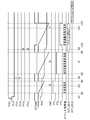
- FIG. 10 is a diagram illustrating an example of the operation of the imaging apparatus.
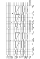
- FIG. 10 is a diagram illustrating an example of an equivalent circuit and an example of an operation of an imaging apparatus according to another embodiment.
- FIG. 10 is a diagram illustrating an example of an equivalent circuit and an example of an operation of an imaging apparatus according to another embodiment.
- FIG. 10 is a diagram illustrating an example of an equivalent circuit of another form of a pixel and an example of a cross section of the pixel.
- FIG. 10 is a diagram illustrating an example of an equivalent circuit of another form of a pixel and an example of a cross section of the pixel. The figure which showed an example of operation
- movement of a pixel of another form The figure which showed an example of arrangement
- movement of a pixel of another form The figure which showed an example of arrangement
- 1 is a block diagram schematically showing an imaging system.
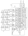
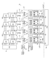
- FIG. 1A shows an example of an equivalent circuit of a pixel according to the present embodiment.
- Reference numerals 1 and 51 denote photoelectric conversion units.
- the photoelectric conversion unit is a photodiode.
- 20 and 50 are transfer MOS transistors
- 4 is a reset MOS transistor
- 5 is an amplification MOS transistor
- 6 is a selection MOS transistor.
- VSC Vertical Scanning Circuit
- H level High level
- L level Low level
- the signal charge held by the photodiode 1 is transferred to the gate of the amplification MOS transistor 5.
- the gate of the amplification MOS transistor 5 is the control electrode of the amplification MOS transistor 5.
- the transfer pulse PTX2 supplied from the vertical scanning circuit 2 is similarly set to the H level at the gate of the transfer MOS transistor 50, the signal charge held by the photodiode 51 is transferred to the gate of the amplification MOS transistor 5.
- the amplification MOS transistor 5 outputs an electrical signal to the selection MOS transistor 6 based on the signal charge transferred to the gate.
- the selection MOS transistor 6 outputs the signal output from the amplification MOS transistor 5 to the vertical signal line 7 when the selection pulse PSEL supplied from the vertical scanning circuit 2 to the gate is at the H level.
- a signal output from the pixel 100 to the vertical signal line 7 corresponds to the pixel signal described above.
- a current is supplied from the current source 8 to the vertical signal line 7 in each column.
- the analog signal output unit of this embodiment includes the pixel 100.
- the signal output to the vertical signal line 7 based on the potential of the gate of the amplification MOS transistor 5 is expressed as a PN signal after setting the reset pulse PRES to the H level and then to the L level.
- the PN signal is a noise signal output to the vertical signal line 7 when the gate potential of the amplification MOS transistor 5 is set to the reset level.
- This PN signal is a first signal output from an analog signal output unit including pixels.
- a signal output to the vertical signal line 7 based on the potential of the gate of the amplification MOS transistor 5 to which the signal charge from the photodiode 1 has been transferred is represented as a P (A + N) signal.
- the P (A + N) signal is a signal in which a PA signal based on a signal charge generated by one photodiode 1 among a plurality of photodiodes is superimposed on the PN signal.
- the P (A + N) signal is the second signal output from the analog signal output unit.
- a signal output to the vertical signal line 7 based on the potential of the gate of the amplification MOS transistor 5 at this time is expressed as a P (A + B + N) signal.
- the P (A + B + N) signal is a signal in which a P (A + B) signal based on the signal charges generated by the plurality of photodiodes 1 and 51 is superimposed on the PN signal.
- the P (A + B + N) signal is the third signal output from the analog signal output unit.
- the first, second, and third signals are analog signals. The above is the description of the pixel 100.
- a comparator 9 (indicated as Comp (Comparator) in FIG. 1B) 9 compares the ramp signal Vramp with a signal output from the pixel 100 to the vertical signal line 7, and performs comparison based on the comparison result.
- the result signal CMP is output to the latch selection circuit 12 (denoted Latch Pulse Gen in FIG. 1B).
- the ramp signal Vramp is a reference signal that is generated by a ramp signal generation circuit (indicated as Ramp Gen. (Ramp Generator) in FIG. 1B) 10 and changes in potential depending on time.
- the ramp signal generation circuit 10 is supplied with an analog / digital converter reset pulse AD Reset from a timing generator (not shown) in common with a first counter 18 described later.
- the latch selection circuit 12 is provided corresponding to a column of a plurality of pixels 100 arranged in a matrix.
- the latch selection circuit 12 outputs the comparison result signal CMP to any one of Latch_n13-1, Latch_a13-2, and Latch_b13-3 according to the signal values of the latch selection pulses PTn, PTa, and PTb. For example, if the latch selection pulse PTn is at the H level and the other latch selection pulses PTa and PTb are at the L level, the latch selection circuit 12 outputs the comparison result signal CMP to Latch_n 13-1.
- Latch_n13-1, Latch_a13-2, and Latch_b13-3 are collectively referred to as a latch circuit 13.
- the latch circuit 13 is a memory unit and is provided corresponding to a column of a plurality of pixels 100 arranged in a matrix.
- Latch_n 13-1 is a first signal holding unit that holds a digital signal obtained by converting the PN signal that is the first signal.
- Latch_a 13-2 holds a digital signal obtained by converting the P (A + N) signal.
- Latch_b 13-3 holds a digital signal obtained by converting the P (A + B + N) signal.
- Latch_a13-2 and Latch_b13-3 are second signal holding units that hold digital signals obtained by converting the P (A + N) signal of the second signal and the P (A + B + N) signal of the third signal.
- the analog-digital conversion unit 16 includes a plurality of circuit units 21.
- the plurality of circuit units 21 are provided corresponding to each column of pixels.
- the circuit unit 21 includes a comparator 9, a latch selection circuit 12, and a latch circuit 13.
- a clock pulse signal clk and an analog-to-digital converter reset pulse AD Reset are output from a timing generator (not shown) to the first counter 18 (indicated as Counter in FIG. 1B).
- the first counter 18 generates a count signal obtained by counting the clock pulse signal clk from when the ramp signal generation circuit 10 starts changing the potential of the ramp signal Vramp depending on time to when it ends.
- Latch_n 13-1, Latch_a 13-2, and Latch_b 13-3 of the latch circuit 13 each hold a count signal when the comparison result signal CMP output from the comparator 9 changes.
- a horizontal scanning circuit (indicated as HSC (Horizontal Scanning Circuit) in FIG.
- the difference signal output unit 15-1 outputs a digital A + B signal, which is a difference signal between the digital A + B + N signal and the digital N signal, as an OUT_b output.
- the digital N signal and the digital A + N signal are output to the differential signal output unit 15-2.
- the difference signal output unit 15-2 outputs a digital A signal, which is a difference signal between the digital A + N signal and the digital N signal, as an OUT_a output.
- the digital A + B signal and the digital A signal are signals output from the image pickup apparatus in the present embodiment.
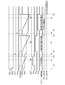
- FIGS. 1A and 1B Next, the operation of the imaging apparatus illustrated in FIGS. 1A and 1B will be described with reference to FIG.
- the selection pulse PSEL and the analog / digital converter reset pulse AD Reset are set to the H level.
- the analog-digital conversion unit reset pulse AD Reset is supplied to each of the ramp signal generation circuit 10 and the first counter 18 in FIG. 1B.
- the analog-digital conversion unit reset pulse AD Reset is at the H level, the potential of the ramp signal Vramp becomes the reset level, and the count signal of the first counter 18 is reset to the initial value.
- the reset pulse PRES is changed from H level to L level.
- a signal that is released from reset at time t11 and is output from the pixel 100 to the vertical signal line 7 is a PN signal.
- the analog-to-digital converter reset pulse AD Reset is changed from H level to L level. Then, the ramp signal Vramp starts changing the potential depending on time. The first counter 18 starts counting the clock pulse signal clk and outputs the count signal to the latch circuit 13 in each column. Further, the latch selection pulse PTn is set to the H level.
- the comparator 9 outputs the comparison result signal CMP to the latch selection circuit 12. Since the latch selection pulse PTn is at the H level, the comparison result signal CMP is output to Latch_n 13-1. Latch_n 13-1 holds a count signal when the comparison result signal CMP is output. Since the count signal value at this time is “4”, a count signal of “4” is held in Latch_n 13-1. The count signal “4” held in the latch_n 13-1 is a digital N signal.
- the count signal value is represented by a decimal number for convenience, but in reality, the count signal held by Latch_n 13-1 is a value obtained by converting the decimal number “4” into a binary number.
- the count signal value is represented by a decimal number.
- the analog-digital conversion unit reset pulse AD Reset is changed from L level to H level, and the change in potential depending on the time of the ramp signal Vramp is completed. Further, the latch selection pulse PTn is changed from H level to L level.
- the transfer pulse PTX1 is changed from L level to H level.
- the charge accumulated in the photodiode 51 is transferred to the gate of the amplification MOS transistor 5, and a P (A + N) signal is output from the pixel 100 to the vertical signal line 7.
- the analog-digital converter reset pulse AD Reset is changed from H level to L level. Then, the ramp signal Vramp starts changing the potential depending on time. The first counter 18 starts counting the clock pulse signal clk and outputs the count signal to the latch circuit 13 in each column. Further, the latch selection pulse PTa is set to the H level.
- the comparator 9 outputs the comparison result signal CMP to the latch selection circuit 12. Since the latch selection pulse PTa is at the H level, the comparison result signal CMP is output to Latch_a 13-2. Latch_a 13-2 holds a count signal when the comparison result signal CMP is output. Since the count signal value at this time is “6”, the count signal “6” is held in Latch_a 13-2. The count signal “6” held in the latch_a 13-2 is a digital A + N signal.
- the analog-to-digital converter reset pulse AD Reset is changed from L level to H level, and the change in potential depending on the time of the ramp signal Vramp is completed. Further, the latch selection pulse PTa is changed from H level to L level. Further, the horizontal scanning circuit 14 causes the difference signal output unit 15-2 to output the count signals held from each of the latch_n 13-1 and the latch_a 13-2. The difference signal output unit 15-2 performs difference processing between the count signal “6” held in the latch_a 13-2 and the count signal “4” held in the latch_n 13-1, and outputs the count signal “2” to the OUT_a Output as output. The count signal “2” is a digital A signal.
- the transfer pulse PTX2 is changed from L level to H level.
- the charge accumulated in the photodiode 1 is transferred to the gate of the amplification MOS transistor 5, and a P (A + B + N) signal is output from the pixel 100 to the vertical signal line 7.
- the analog-digital converter reset pulse AD Reset is changed from H level to L level. Then, the ramp signal Vramp starts changing the potential depending on time. The first counter 18 starts counting the clock pulse signal clk and outputs the count signal to the latch circuit 13 in each column. Further, the latch selection pulse PTb is set to the H level.
- the comparator 9 outputs the comparison result signal CMP to the latch selection circuit 12. Since the latch selection pulse PTb is at the H level, the comparison result signal CMP is output to Latch_b 13-3. Latch_b 13-3 holds a count signal when the comparison result signal CMP is output. Since the count signal value at this time is “8”, the count signal of “8” is held in Latch_b 13-3. The count signal of “8” held in Latch_b 13-3 is a digital A + B + N signal.
- the analog-digital conversion unit reset pulse AD Reset is changed from L level to H level, and the change in potential depending on the time of the ramp signal Vramp is completed. Further, the latch selection pulse PTb is changed from H level to L level. Further, the horizontal scanning circuit 14 causes the difference signal output unit 15-1 to output the count signal held from each of the latch_n 13-1 and the latch_b 13-3. The difference signal output unit 15-1 performs difference processing between the count signal “8” held in the latch_b 13-3 and the count signal “4” held in the latch_n 13-1, and outputs the count signal “4” to the OUT_b Output as output. The count signal “4” is a digital A + B signal.
- the imaging apparatus of this embodiment can output a digital A signal and a digital A + B signal.
- the latch circuit 13 holds the digital N signal, the digital A + N signal, and the digital A + B + N signal.
- the imaging apparatus of the present embodiment can obtain the digital A signal and the digital A + B signal with high accuracy.
- an operation variation component for each comparator of the plurality of comparators 9 is included.
- the imaging apparatus of the present embodiment subtracts the digital N signal from the digital A + N signal and the digital A + B + N signal and outputs the result.
- the noise component of the pixel 100 included in the digital A + N signal and the digital A + B + N signal can be subtracted from the operation variation component of each comparator of the plurality of comparators 9, thereby reducing deterioration in image quality. it can.
- the differential signal output unit 15-2 outputs a digital A signal.
- This digital A signal is a first difference signal between a digital A + N signal obtained by converting the second signal and a digital N signal obtained by converting the first signal.
- the differential signal output unit 15-1 outputs a digital A + B signal.
- the digital A + B signal is a second difference signal between the digital A + B + N signal obtained by converting the third signal and the digital N signal obtained by converting the first signal.
- the signal value of the PN signal may vary due to variations in capacitance values of a plurality of capacitors that hold the PN signal.
- the PN signal is held in the latch circuit Latch_n 13-1 as a digital N signal. Therefore, it is possible to suppress variations in the PN signal due to being held in different capacitors.
- the imaging device having the pixel 100 having the two photodiodes 1 and 51 has been described.
- the present embodiment is not limited to this form.
- This embodiment can also be preferably implemented in an imaging apparatus having a pixel 100 having one photodiode. That is, in the pixel 100 illustrated in FIG. 1A, the photodiode 51 and the transfer MOS transistor 50 may be omitted.
- the transfer pulse PTX2 may be set to H level at time t15 and time t19. First, the transfer pulse PTX2 is set to H level at time t15, whereby the signal charge generated by the photodiode 1 is transferred to the gate of the amplification MOS transistor 5.
- the signal output here is the second signal.
- the transfer pulse PTX2 is set to the L level.
- the photodiode 1 again performs photoelectric conversion based on the incident light to generate signal charges.
- the transfer pulse PTX2 is again set to the H level.
- the signal charge accumulated in the photodiode 1 is transferred to the gate of the amplification MOS transistor 5.
- the gate of the amplification MOS transistor 5 holds the signal charge transferred from the photodiode 1 at time t15 and the signal charge transferred at time t19.
- the signal output from the pixel 100 is the third signal.
- the second signal and the third signal may be signals based on signal charges generated by changing the exposure time of the photodiode 1.
- the pixel 100 may have a different form from that described so far in this embodiment. That is, the first signal output to the vertical signal line 7 by setting the gate potential of the amplification MOS transistor 5 to the reset level and m (m is a natural number) of the plurality of photodiodes included in the pixel 100.
- the latch_n 13-1 shows a form in which one digital N signal is held, but a double buffer memory having a plurality of memories capable of holding the digital N signal may be used. That is, the first memory included in Latch_n 13-1 holds the digital N signal obtained by converting the PN signal of the pixel in the first row of this embodiment at time t14. Then, the digital N signal is transferred from the first memory to the second memory during any period from time t14 to time t18. The horizontal scanning circuit 14 outputs the digital N signal from the second memory to the differential signal output unit 15-2.
- the selection pulse PSEL is set to L level at time t22, and the selection pulse PSEL and reset pulse PRES of the pixel 100 in the next row are set to H level.
- the analog / digital conversion unit reset pulse AD Reset is changed from H level to L level, and an operation of generating a digital signal obtained by converting the PN signal of the pixel 100 in the next row is performed.
- the latch_n 13-1 performs in parallel the output of the digital N signal to the differential signal output unit 15-1 and the generation of the digital N signal obtained by converting the PN signal of the pixel 100 in the next row from time t22. be able to. Accordingly, it is possible to reduce the time required for generating and outputting a digital signal obtained by converting the signals output from the pixels 100 in a plurality of rows.
- a digital signal may be transferred from Latch_a 13-2 to Latch_b 13-2, and the horizontal scanning circuit 14 may output a digital signal from Latch_b 13-2.
- Latch_a 13-2 transfers the held digital A + N signal to Latch_b 13-3.
- the horizontal scanning circuit 14 outputs a digital A + N signal from Latch_b 13-3.
- the latch_a 13-2 holds a digital A + B + N signal obtained by counting the clock pulse signal clk and converting the P (A + B + N) signal during a period from time t20 to time t22. At time t22, the latch_a 13-2 transfers the held digital A + B + N signal to the latch_b 13-3.
- the horizontal scanning circuit 14 transfers the digital A + B + N signal from Latch_b 13-3 to the differential signal output unit 15.
- a plurality of differential signal output units 15-1 and 15-2 provided in the present embodiment can be made into one differential signal output unit 15.
- the analog-digital conversion unit of the present embodiment has a format that performs AD conversion based on a comparison between a ramp signal whose potential changes depending on time and a pixel signal. May be a delta sigma type or the like.
- the imaging apparatus according to the present embodiment will be described with a focus on differences from the first embodiment.
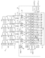
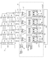
- FIG. 3A is an equivalent circuit diagram illustrating an example of the imaging apparatus of the present embodiment.
- Components having the same functions as those in FIG. 1B described in the first embodiment are denoted by the same reference numerals as those in FIG. 1B.
- the difference from the first embodiment is that the PN signal, P (A + N) signal, and P (A + B + N) signal output from the pixel 100 are inverted and amplified by the inverting amplifier 17 and output to the comparator 9.
- the inverting amplifier 17 is an amplifying unit that amplifies the pixel signal and outputs it to the comparator 9.
- the plurality of inverting amplifiers 17 are provided corresponding to the columns of the plurality of pixels 100 arranged in a matrix. For the vertical signal line 7, the electrical path from the pixel 100 to the inverting amplifier 17 is shown separately from the vertical signal line 7-1, and the electrical path from the inverting amplifier 17 to the comparator 9 is shown separately from the vertical signal line 7-2. .
- the analog signal output unit of this embodiment includes the pixel 100 and the inverting amplifier 17.
- a signal output from the inverting amplifier 17 is supplied to the comparator 9 based on the PN signal output from the pixel 100.
- a signal output from the inverting amplifier 17 based on the PN signal output from the pixel 100 is referred to as a GN signal.
- a signal output from the inverting amplifier 17 based on the P (A + N) signal output from the pixel 100 is a G (A + N) signal
- a signal output from the inverting amplifier 17 based on the P (A + B + N) signal is G (A + B + N). Indicated as a signal.
- the first signal output from the analog signal output unit is a GN signal.
- the second signal output from the analog signal output unit is a G (A + N) signal.
- the third signal output from the analog signal output unit is a G (A + B + N) signal.
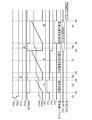
- FIG. 3B is a timing diagram illustrating an example of the operation of the imaging apparatus illustrated in FIG. 3A.
- the potential corresponding to the vertical signal line 7-1 of the present embodiment is shown as the potential Vline of the vertical signal line 7.
- FIG. 3B of the present embodiment shows the potential Vline2 of the vertical signal line 7-2 which is an electrical path from the inverting amplifier 17 to the comparator 9.
- the potential Vline2 of the vertical signal line 7-2 is a signal obtained by inverting and amplifying the potential of the vertical signal line 7-1, it is opposite to the electrical polarity of the vertical signal line 7-1. Therefore, in this embodiment, the direction in which the potential Vline2 of the vertical signal line 7-2 changes when the P (A + N) signal and the P (A + B + N) signal are output from the pixel 100 is opposite to that in the first embodiment. Become. Therefore, the direction in which the potential changes depending on the time of the ramp signal Vramp is also opposite to that in the first embodiment.
- the digital N signal held by Latch_n 13-1 is a signal obtained by converting the GN signal into a digital signal.
- the digital N signal of the present embodiment is a signal including a noise component of an analog signal output unit including the pixel 100 and the inverting amplifier 17 and an operation variation component for each comparator of the plurality of comparators 9.
- the digital A + N signal held by Latch_a 13-2 is a signal obtained by converting the G (A + N) signal output from the pixel 100 into a digital signal.
- the digital A + B + N signal held by Latch_b 13-3 is a signal obtained by converting the G (A + B + N) signal into a digital signal.
- the digital N signal of this embodiment includes a component of operation variation for each comparator of the plurality of comparators 9 in addition to the noise component of the analog signal output unit including the pixel 100 and the inverting amplifier 17.
- the imaging apparatus of the present embodiment subtracts the digital N signal from the digital A + N signal and the digital A + B + N signal and outputs the result. Accordingly, the noise component of the analog signal output unit including the pixel 100 and the inverting amplifier 17 included in the digital A + N signal and the digital A + B + N signal and the operation variation component of each comparator of the plurality of comparators 9 can be subtracted. And a reduction in image quality can be reduced.
- the inverting amplifier 17 may be replaced with a non-inverting amplifier or a buffer circuit.
- the direction in which the potential Vline2 and the ramp signal Vramp change coincides with the potential Vline and the ramp signal Vramp shown in FIG.
- the imaging apparatus of the present embodiment will be described focusing on differences from the second embodiment.
- FIG. 4A is an equivalent circuit diagram illustrating an example of the imaging apparatus of the present embodiment.
- the image pickup apparatus does not include the latch selection circuit 12 but includes a counter control circuit 16 corresponding to each column of pixels.
- the first counter 18 supplies a common count signal to the latch circuits 13 in each column.
- the second counter 19 is connected to the counter control circuit 16 in each column.
- a memory 25 for holding the signal of the second counter 19 is provided corresponding to the second counter 19 in each column.
- the memory 25 that holds the signal of the second counter 19 is a first signal holding unit that holds a digital N ′ signal generated based on the GN signal output from the inverting amplifier 17. Further, the memory 25 outputs a digital N ′ signal to the second counter 19 in the comparison between the third signal and the ramp signal Vramp.
- the counter control circuit 16 receives a clock pulse signal clk from a timing generator (not shown). Furthermore, the counter control circuit 16 operates the second counter 19 and the memory 25 based on the count signal reset pulse CNT Reset, the pulse transtom, and the pulse transoc.
- the latch 26 holds the count signal of the second counter 19.
- the second signal holding unit that holds the digital signal obtained by converting the second signal and the digital signal obtained by converting the third signal has two signals, Latch_a13-1 and Latch_b13-2.
- the latch 26 is a second signal holding unit that holds a digital signal obtained by converting the second signal and a digital signal obtained by converting the third signal according to this embodiment.
- the latch signal LAT is given to the latch 26 of each column, and the count signal value output from the second counter 19 is fetched when the latch signal LAT is at the H level.
- the ramp signal generation circuit 10 is supplied with a lamp reset pulse Ramp Reset that resets the potential of the ramp signal to an initial value.
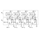
- FIG. 4B is an equivalent circuit diagram illustrating the second counter 19 and the memory 25 of the imaging apparatus illustrated in FIG. 4A.
- the second counter 19 includes a plurality of flip-flop circuits FF1-1 to FF1-4 that generate count signals. That is, the second counter 19 has a plurality of flip-flop circuits FF1-1 to FF1-4 that generate count signals including a plurality of bit signals.
- the bit signal is a signal of each bit of the count signal.
- the memory 25 serving as the first signal holding unit includes a plurality of bit memories 250-1 to 250-4, and each of the plurality of bit memories 250-1 to 250-4 includes a plurality of flip-flop circuits FF1-1 to FF1-1. It is electrically connected to each of FF1-4.
- the memory 25 has a plurality of bit memories 250-1 to 250-4 for holding each of the bit signals, and each of the plurality of bit memories is electrically connected to each of the plurality of flip-flop circuits FF1-1 to FF1-4.
- the second counter 19 of this embodiment is configured to electrically connect a plurality of flip-flop circuits FF1-1 to FF1-4 and to input the output of the non-inverting output terminal Q at the previous stage to the clock terminal at the subsequent stage. .
- the outputs D0 to D3 of the non-inverted outputs Q of the flip-flop circuits FF1-1 to FF1-4 are output to the latch 26 and given to the bit memories 250-1 to 250-4, respectively.
- each of the flip-flop circuits FF1-1 to FF1-4 supplies the output of its inverting output terminal NQ to the terminal D, and outputs the output of the inverting output terminal NQ to the respective bit memory 250. -1 to 250-4.
- the signals held in the bit memories 250-1 to 250-4 are output to the S terminals of the flip-flop circuits.
- FIG. 5 is a timing chart showing an example of the operation of the imaging apparatus described in FIGS. 4A and 4B.
- the counter control pulse is a signal output from the counter control circuit 16 to the second counter 19, and the second counter 19 operates based on the counter control pulse.
- the selection pulse PSEL and the ramp signal reset pulse Ramp Reset are set to the H level.
- the reset pulse PRES is changed from H level to L level.
- the counter control pulse is in a “stop” state in which the second counter 19 does not operate.
- the ramp signal reset pulse Ramp Reset is changed from H level to L level. Then, a change in potential depending on the time of the ramp signal Vramp is started.
- the comparator 9 outputs a comparison result signal CMP to the counter control circuit 16.
- the counter control circuit 16 receives the comparison result signal CMP and changes the counter control pulse from the “stop” state to the “count” state.
- the second counter 19 starts counting from time t53.
- the change in potential depending on the time of the ramp signal Vramp is completed, and the ramp signal reset pulse Ramp Reset is changed from L level to H level. Further, the counter control pulse is changed from the “count” state to the “stop” state. As a result, the second counter 19 temporarily stops the counting operation at time t54. Further, the pulse transtom is set to the H level. Thereby, the count signal value obtained by counting from the time t53 to the time t54 is held in the memory 25. At this time, the signal held in the memory 25 is a digital N ′ signal. Then, the pulse transtom is set to the L level.
- the transfer pulse PTX1 is changed from L level to H level.
- the charge accumulated in the photodiode 51 is transferred to the gate of the amplification MOS transistor 5, and a P (A + N) signal is output from the pixel 100 to the vertical signal line 7.
- a G (A + N) signal is output from the inverting amplifier 17 to the comparator 8.
- the ramp signal reset pulse Ramp Reset is changed from H level to L level. Then, a change in potential depending on the time of the ramp signal Vramp is started. Further, the counter control pulse is changed from the “stop” state to the “count” state. As a result, the second counter 19 starts counting from the count signal value at time t54.
- the comparator 9 outputs a comparison result signal CMP to the counter control circuit 16.
- the counter control circuit 16 receives the comparison result signal CMP, and changes the counter control pulse from the “count” state to the “stop” state.
- the second counter 19 holds a count signal obtained by counting a period from time t56 to time t57 from the count signal value at time t54.
- the ramp signal reset pulse Ramp Reset is changed from the L level to the H level, and the change in potential depending on the time of the ramp signal Vramp is completed. Further, the latch signal LAT is set to the H level. As a result, the count signal held by the second counter 19 at this time t58 is taken into the Latch 26.
- the second counter 19 holds a digital N ′ signal that is a count signal value obtained by counting the period from time t53 to time t54 when the comparator 9 outputs the comparison result signal CMP. .
- This count signal value is derived from the maximum count signal value Nmax at the time of N conversion (that is, the count signal value obtained by counting all the periods from time t52 to time t54 when the ramp signal Vramp starts changing the potential depending on time), This is a count signal value (Nmax ⁇ Ncnt) obtained by subtracting the count signal value Ncnt counted from time t52 to time t53.
- the count signal value Ncnt is held by the Latch_n 13-1.
- the count signal value (Nmax ⁇ Ncnt) is held by the Latch 26.
- the second counter 19 holds the count signal value (Nmax ⁇ Ncnt). Therefore, the second counter 19 starts the count operation from the time t56 to the time t57 from the count signal value (Nmax ⁇ Ncnt).
- the count signal value held by the second counter 19 at time t58 is the count signal when the period from time t56 to time t57 is counted from the initial count signal value (that is, the count signal value at time t52). This is a value obtained by adding the count signal value (Nmax ⁇ Ncnt) to the value Acnt + Ncnt.
- the count signal value at time t58 is expressed as Acnt + Ncnt + (Nmax ⁇ Ncnt), that is, Acnt + Nmax. Therefore, a digital signal that does not include a component of the GN signal and in which an offset of Nmax is added to the digital A signal is held in the latch 26.
- the digital signal having the count signal value of Acnt + Nmax is a digital signal obtained by converting the GA signal output based on the PA signal.
- the known maximum count signal value Nmax at the time of N conversion is subtracted from the count signal value Acnt + Nmax held by the second counter 19 at time t58. Thereby, the count signal value Acnt, that is, the digital A signal can be obtained.
- the latch signal LAT is set to H level, and then the latch signal LAT is set to L level.
- the pulse transoc is set to H level, and the count signal value of the second counter 19 is returned to the count signal value at time t54. That is, the count signal value is the signal value of the digital N ′ signal. Further, the horizontal scanning circuit 14 sequentially selects the latches 26 of each column and outputs a digital A signal held by the latches 26.
- the transfer pulse PTX2 is changed from L level to H level.
- the charge accumulated in the photodiode 1 is transferred to the gate of the amplification MOS transistor 5, and a P (A + B + N) signal is output from the pixel 100 to the vertical signal line 7.
- the G (A + B + N) signal is output from the inverting amplifier 17 to the comparator 8.
- the ramp signal reset pulse Ramp Reset is changed from H level to L level. Then, a change in potential depending on the time of the ramp signal Vramp is started. Further, the counter control pulse is changed from the “stop” state to the “count” state. Thereby, the second counter 19 starts the count operation from the count signal value at time t54 (that is, the count signal value at time t59).
- the comparator 9 outputs a comparison result signal CMP to the counter control circuit 16.
- the counter control circuit 16 receives the comparison result signal CMP, and changes the counter control pulse from the “count” state to the “stop” state.
- the second counter 19 holds a count signal obtained by counting a period from time t61 to time t62 from the count signal value at time t54.
- the digital signal captured by the latch 26 at this time will be described.
- An operation during the period from time t61 to time t63 (hereinafter referred to as A + B + N conversion) will be described.
- the second counter 19 holds the count signal value (Nmax ⁇ Ncnt). Therefore, the second counter 19 starts the count operation from the time t61 to the time t62 from the count signal value (Nmax ⁇ Ncnt).
- the count signal value held by the second counter 19 at time t62 is the count signal when the period from time t61 to time t62 is counted from the initial count signal value (that is, the count signal value at time t52).
- the count signal value at time t58 is expressed as Acnt + Bcnt + Ncnt + (Nmax ⁇ Ncnt), that is, Acnt + Bcnt + Nmax. Therefore, the digital signal which does not include the component of the GN signal and in which the offset of Nmax is added to the digital A + B signal is held in the latch 26.
- the digital signal having the count signal value of Acnt + Bcnt + Nmax is a digital signal obtained by converting the G (A + B) signal output based on the P (A + B) signal.
- the known maximum count signal value Nmax at the N conversion is subtracted from the count signal value Acnt + Bcnt + Nmax held by the second counter 19 at time t63. Thereby, the count signal value Acnt + Bcnt, that is, the digital A + B signal can be obtained.
- the latch signal LAT is set to L level after the latch signal LAT is set to H level.
- the count signal reset pulse CNT Reset is set to H level. Thereby, the signal value of the count signal of the second counter 19 is reset to the initial value. Further, the horizontal scanning circuit 14 sequentially selects the latches 26 of each column, and outputs a digital signal held by the latch 26 at time t63.
- the process of subtracting Nmax from the digital signal held by the latch 26, which is performed to obtain the digital A signal and the digital A + B signal, may be performed in the imaging apparatus or is not shown in the figure that is electrically connected to the imaging apparatus. You may perform by a signal processing part.
- the circuit unit 21 provided in each column of this embodiment includes a comparator 9, a counter control circuit 16, a second counter 19, a memory 25, and a latch 26.
- the circuit unit 21 in each column outputs a digital A signal.
- This digital A signal is a first difference signal between a digital A + N signal obtained by converting the second signal and a digital N signal obtained by converting the first signal.
- the circuit unit 21 in each column outputs a digital A + B signal.
- the digital A + B signal is a second difference signal between the digital A + B + N signal obtained by converting the third signal and the digital N signal obtained by converting the first signal.
- a digital A signal and a digital A + B signal can be acquired.
- the digital signal held by the latch 26 can be a signal that does not include the component of the GN signal obtained by converting the PN signal. That is, according to the operation of this embodiment, the operation of comparing the pixel signal and the ramp signal Vramp and the operation of obtaining the digital signal obtained by converting the signal obtained by subtracting the N signal from the A + N signal and the A + B + N signal can be performed in parallel. .
- the imaging apparatus of the present embodiment will be described focusing on differences from the third embodiment.
- FIG. 6A is an equivalent circuit diagram illustrating an example of the imaging apparatus of the present embodiment.
- the imaging apparatus according to the present embodiment is different from the third embodiment in that a mode setting pulse mode is given to the second counter 19 from a timing generator (not shown) via the counter control circuit 16.
- the mode setting pulse mode is a pulse for switching the mode of the second counter 19 described later.
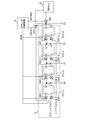
- FIG. 6B is an equivalent circuit diagram showing the second counter 19 of this embodiment illustrated in FIG. 6A.
- the second counter 19 of this embodiment is configured to electrically connect the flip-flop circuits FF2-1 to FF2-4 and to input the output from the non-inverting output terminal Q at the previous stage to the clock terminal at the subsequent stage.
- the outputs of the non-inverting output terminals Q of the flip-flop circuits FF2-1 to 2-4 are given to the latch 26 as D0 to D3.
- the counter control circuit 16 is electrically connected to the switches SW3-1 to 3-4 and the clock pulse terminals which are electrically connected to the terminals D of the flip-flop circuits FF2-1 to 2-4, respectively. Further, the mode setting pulse mode for switching the mode is given to the switches SW4-1 to 4-4.
- a timing generator (not shown) supplies a pulse transc to the switch SW1 and a pulse transm to the switch SW2 via the counter control circuit 16.
- the mode setting pulse mode is at the L level
- the inverting output terminals NQ of the flip-flop circuits FF2-1 to 2-4 are electrically connected to the terminal D of its own flip-flop circuit.
- the clock pulse terminal is given a count CLK.
- the terminals D of the flip-flop circuits FF2-1 to FF2-4 are electrically connected to the non-inverting output terminal Q of the preceding flip-flop circuit, respectively.
- the shift CLK is given to the clock pulse terminals of the flip-flop circuits FF2-1 to 2-4.
- the pulse transm applied to the switch SW2 is at the H level, the non-inverting output terminal Q of the flip-flop circuit FF2-4 and the memory 25 are electrically connected. Therefore, when the mode setting pulse mode and the pulse transtom are both at the H level, signals output from the flip-flop circuits FF2-1 to FF2-4 are sequentially output to the memory 25.
- the memory 25 is a shift register circuit, for example, and holds count signals having signals output from the flip-flop circuits FF2-1 to FF2-4 that are sequentially output.
- the flip-flop circuit FF2-1 is electrically connected to the memory 25 via the switch SW1.
- the count signal held in the memory 25 is sequentially supplied to the flip-flop circuits FF2-1 to FF2-4.
- FIG. 7 is a timing diagram illustrating an example of the operation of the imaging apparatus illustrated in FIG. 6A. In the following, a description will be given focusing on differences from the operation described in Embodiment 3 with reference to FIG.
- the mode setting pulse mode is at the L level.
- the rest can be the same as the operation at time t51 shown in FIG.
- the operation from time t72 to time t74 can be the same as the operation from time t52 to time t54 shown in FIG.
- the mode setting pulse mode and the pulse transtom are set to the H level.
- the count signal value at time t74 is held in the memory 25.
- the mode setting pulse mode and the pulse transoc are set to the H level.
- the count signal value at time t74 held in the memory 25 during any period from time t74 to time t76 is set in the second counter 19.
- time t78 to time t80 can be the same as those from time t58 to time t61 shown in FIG.
- time t81 to time t83 can also be the same as the operation from time t62 to time t64 shown in FIG.
- a digital A signal and a digital A + B signal can be acquired.
- focus detection is performed by a phase difference detection method using a pixel signal output from a pixel 100 provided in an imaging apparatus.
- FIG. 8A is an equivalent circuit diagram illustrating an example of a pixel having four photoelectric conversion units, that is, photodiodes 1, 51, 61, and 71.
- the signal charges generated by the photodiodes 1, 51, 61 and 71 are transferred to the gate of the amplification MOS transistor 5 through the transfer MOS transistors 20, 50, 60 and 70, respectively.
- a transfer pulse PTX1 is applied to the gate of the transfer MOS transistor 20 from the vertical scanning circuit 2 in the same manner as in the imaging device described with reference to FIG. 1B.
- a transfer pulse PTX2 is transferred to the transfer MOS transistor 50
- a transfer pulse PTX3 is transferred to the transfer MOS transistor 60
- a transfer pulse PTX4 is transferred to the transfer MOS transistor 70 from the vertical scanning circuit 2 as in the image pickup apparatus described with reference to FIG. 1B.
- the image pickup apparatus according to the present embodiment can be implemented with any of the configurations described in the first to fourth embodiments of the analog-digital conversion unit, but in the following, the analog-digital conversion unit 16 according to the first embodiment is used.
- the image pickup apparatus will be described.
- FIG. 8B is a cross-sectional view including two photodiodes included in the pixel 100 in FIG. 8A.
- FIG. 8B shows a so-called back-illuminated imaging device in which photodiodes 1, 51, 61, 71 are arranged between one microlens 23 and the circuit unit 200.
- the form of the present embodiment can be suitably implemented even with a back-illuminated imaging device.
- the circuit unit 200 and the photodiodes 1, 51, 61, and 71 may be formed on different substrates, and a back-illuminated imaging device may be formed by electrical connection therebetween. An example of how to separate the substrates is shown by ⁇ - ⁇ line segments.
- an inner lens may be further provided between the microlens 23 and the photodiodes 1, 51, 61, 71 to improve the light collection efficiency to the photodiode.
- FIG. 9 is a timing chart showing an example of the operation of the imaging apparatus of FIG. 8A. The description will focus on the differences from the timing described with reference to FIG. 2 in the first embodiment.
- the operation from time t91 to t94 can be the same as the operation from time t11 to time t14 in the first embodiment.
- both transfer pulses PTX1 and PTX2 are set to H level.
- signal charges generated by the photodiodes 1 and 51 are transferred to the gate of the amplification MOS transistor 5.
- the pixel signal output to the vertical signal line 7 is obtained by superimposing the sum of the PA signal based on the signal charge of the photodiode 1 and the PB signal based on the signal charge of the photodiode 51 on the PN signal.
- a + B + N) signal The signal output operation from the pixel 100 to the vertical signal line 7 at the time t95 is referred to as a first pixel output operation in this embodiment.
- the operation from time t96 to time t98 can be the same as the operation from time t16 to time t18 in the first embodiment. Thereby, a digital A + B + N signal obtained by converting a P (A + B + N) signal into a digital signal is obtained.
- both transfer pulses PTX3 and PTX4 are set to the H level.
- the signal charges generated by the photodiodes 61 and 71 are transferred to the gate of the amplification MOS transistor 5 that already holds the signal charges generated by the photodiodes 1 and 51 at time t96.
- P (A + B + C + D + N) in which a signal obtained by adding the P (A + B) signal, the PC signal based on the signal charge of the photodiode 61, and the PD signal based on the signal charge of the photodiode 71 is superimposed on the PN signal.
- a signal is output to the vertical signal line 7.
- the signal output operation from the pixel 100 to the vertical signal line 7 at time t99 is referred to as a second pixel output operation in this embodiment.
- the operation from time t100 to time t102 can be the same as the operation from time 20 to time t22 in the first embodiment. Thereby, a digital A + B + C + D + N signal obtained by converting the P (A + B + C + D + N) signal into a digital signal can be obtained.
- the differential signal output unit 15-2 outputs a digital A signal.
- This digital A signal is a first difference signal between a digital A + N signal obtained by converting the second signal and a digital N signal obtained by converting the first signal.
- the differential signal output unit 15-1 outputs a digital A + B signal.
- the digital A + B signal is a second difference signal between the digital A + B + N signal obtained by converting the third signal and the digital N signal obtained by converting the first signal.
- a P (A + B + N) signal is output from the pixel 100 to the vertical signal line 7.
- the present invention is not limited to this combination, and the operation of the phase difference detection method can be suitably implemented as long as the signal charge is transferred from two different photodiodes to the gate of the amplification MOS transistor 5. Details will be described later with reference to FIGS. 11B to 11D.
- FIG. 11A shows an example of the arrangement of the pixel 100 having four photodiodes and the microlens 23.
- the imaging apparatus according to the present embodiment includes a microlens array having a plurality of microlenses 23, and one microlens 23 is arranged for one pixel 100.
- A, B, C, and D in FIG. 11A show examples of the arrangement of photodiodes that generate signal charges for obtaining PA, PB, PC, and PD signals, respectively.
- the photodiode 1 described with reference to FIG. 8A is arranged in a region indicated by A.
- FIG. 11B to 11D the signals in the area surrounded by the ellipse are added and output to the vertical signal line 7. That is, in FIG. 11B, the P (A + C) signal or the P (B + D) signal is output from the pixel 100 to the vertical signal line 7 in the first pixel output operation. Similarly, in FIG. 11C, the P (A + B + N) signal or the P (C + D + N) signal is output from the pixel 100 to the vertical signal line 7 in the first pixel output operation. Similarly, in FIG.
- the P (A + D + N) signal or the P (B + C + N) signal is output from the pixel 100 to the vertical signal line 7 in the first pixel output operation.
- the P (A + B + C + D + N) signal is output in any of the forms of FIGS. 11B to 11D.
- the first signal output from the analog signal output unit in the form of FIGS. 11B to 11D is a PN signal.
- the second signal in FIG. 11B is a P (A + C + N) signal or a P (B + D + N) signal.
- the second signal in FIG. 11C is a P (A + B + N) signal or a P (C + D + N) signal.
- the second signal in FIG. 11D is a P (A + D + N) signal or a P (B + C + N) signal.
- the third signal in the form of FIGS. 11B to 11D is a P (A + B + C + D + N) signal.
- FIG. 12 is a schematic diagram when the image pickup apparatus of the present embodiment is applied to a digital still camera as an example of the image pickup system.
- the imaging system includes a barrier 151 for protecting the lens, a lens 152 that forms an optical image of a subject on the imaging device 154 of the present embodiment, a diaphragm 153 for changing the amount of light passing through the lens 152,
- An output signal processing unit 155 that processes an output signal output from the imaging device 154 is provided.
- the output signal processing unit 155 is a digital signal processing unit that processes a digital signal output from the imaging device 154.
- a lens 152 and a diaphragm 153 are optical systems that collect light on the imaging device 154.
- the imaging device 154 outputs a digital signal obtained by converting the second signal and a digital signal obtained by converting the third signal.
- the output signal processing unit 155 can perform differential processing to obtain a digital B signal by subtracting the digital A signal from the digital A + B signal.
- the output signal processing unit 155 performs an operation of outputting a signal after performing various corrections and compression as necessary.
- the imaging system 12 further includes a buffer memory unit 156 for temporarily storing image data, and an external interface unit 157 for communicating with an external computer or the like.
- the imaging system further includes a removable recording medium 159 such as a semiconductor memory for recording or reading imaging data, and a recording medium control interface unit 158 for recording or reading to the recording medium 159.
- the solid-state imaging system further includes a general control / arithmetic unit 1510 that controls various calculations and the entire digital still camera, and a timing supply unit 1511 that outputs various timing signals to the imaging device 154 and the output signal processing unit 155.
- the timing signal or the like may be input from the outside, and the imaging system may include at least the imaging device 154 and the output signal processing unit 155 that processes the output signal output from the imaging device 154.
- a P (A + C + N) signal is output in the first pixel output operation, and a digital A + C + N signal is obtained by digital conversion described with reference to FIG.
- a P (A + B + C + D + N) signal is output, and digital conversion is performed in the same manner as the P (A + C + N) signal to obtain a digital A + B + C + D + N signal.
- the differential signal output unit 15 outputs a digital A + C signal and a digital A + B + C + D signal.
- the output signal processing unit 155 obtains a digital (B + D) ′ signal that is a difference between the digital A + B + C + D signal and the digital A + C signal output from the imaging apparatus.
- This digital (B + D) ′ signal corresponds to a digital B + D signal obtained by digitally converting a P (B + D) signal that is assumed to be output by the pixel 100 although the P (B + D) signal is not output from the pixel 100 in this embodiment. Signal.
- the phase difference due to the photodiode array can be detected to perform focus detection.
- FIG. 11C it is possible to detect a phase difference due to a row of photodiodes and perform focus detection. Further, in FIG. 11D, focus detection can be performed by detecting the phase difference in the oblique direction of the photodiode.
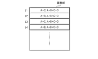
- FIG. 11E schematically shows the pixel portion, and L1 to L4 represent the first to fourth pixel rows in order from the top of the figure.
- the row L1 is described as A + C, A + B + C + D.
- the P (A + C + N) signal which is a signal including the P (A + C) signal
- P (A + B + C + D + N) signal which is a signal including the P (A + B + C + D) signal in the second pixel output operation, is output from the pixel 100 to the vertical signal line 7.
- P (A + B + C + D + N) signal which is a signal including the P (A + B + C + D) signal in the second pixel output operation, is output from the pixel 100 to the vertical signal line 7.
- the phase difference due to the photodiode column can be detected in the pixels 100 in the L1 row, and the phase difference due to the photodiode row can be detected in the pixels 100 in the L2 row.
- the phase difference for each column of the photodiode and for each row can be detected by the pixel 100 of each row.
- a row for detecting the phase difference in the oblique direction of the photodiode may be provided as shown in FIG. 11D.
- the P (A + B + C + D) signal obtained by the second pixel output operation is a pixel signal based on light incident on all photodiodes of the pixel 100. Therefore, in order to obtain an image based on the incident light of the pixel 100, an image may be generated using a digital A + B + C + D signal obtained by converting a P (A + B + C + D) signal.
- FIG. 11F Another form of the signal output operation for each row of the pixel portion will be described with reference to FIG. 11F.
- the reference numerals in FIG. 11F are the same as those in FIG. 11E.
- the pixels 100 in each row have the PN signal, the P (A + N) signal, the P (A + B + N) signal, the P (D + N) signal, and the P (D + C + N) signal on the vertical signal line 7 in a time division manner.
- This output operation will be described with reference to FIG. FIG. 10 will be described on the assumption that Latch_n 13-1 is a double buffer memory having a plurality of memories capable of holding digital N signals.
- the operation from time t111 to time t114 can be the same as the operation from time t91 to time t94 described with reference to FIG.
- the transfer pulse PTX1 is set to H level.
- a P (A + N) signal is output from the pixel 100 to the vertical signal line 7.
- the operation from time t116 to time t118 can be the same as the operation from time t96 to time t98 described with reference to FIG. Thereby, a digital A + N signal obtained by converting a P (A + N) signal into a digital signal is obtained.
- the transfer pulse PTX2 is set to H level.
- a P (A + B + N) signal is output from the pixel 100 to the vertical signal line 7.
- the operation from time t120 to time t122 can be the same as the operation from time t100 to time t102 described with reference to FIG. Thereby, a digital A + B + N signal obtained by converting a P (A + B + N) signal into a digital signal is obtained.
- the reset pulse PRES is set to H level.
- the potential of the gate of the amplification MOS transistor 5 becomes the reset level.
- the operation from time t124 to time t127 can be similar to the operation from the previous time t111 to time t114. Since Latch_n 13-1 is a double buffer memory, this N conversion period and the period during which the digital N signal held at time t114 is transferred to the differential signal output unit 15-1 can be overlapped.
- transfer pulse PTX3 is set to H level.
- a P (D + N) signal is output from the pixel 100 to the vertical signal line 7.
- the operation from time t129 to time t131 can be similar to the operation from the previous time t116 to time 118. Thereby, a digital D + N signal obtained by converting a P (D + N) signal into a digital signal is obtained.
- the transfer pulse PTX4 is set to H level.
- a P (D + C + N) signal is output from the pixel 100 to the vertical signal line 7.
- the operation from time t133 to time t135 can be the same as the operation from the previous time t120 to time t122. Thereby, a digital D + C + N signal obtained by converting the P (D + C + N) signal into a digital signal is obtained.
- the PN signal is converted back to the digital N signal by the operation from time t125 to time t127, but this operation is omitted and only the digital N signal obtained from time t112 to time t115 is used. Also good.
- a digital A signal, a digital A + B signal, a digital D signal, and a digital D + C signal are output from the imaging apparatus.
- the n photoelectric conversion units are photodiodes 1 and 51.
- the p photoelectric conversion units (p is a natural number) different from the n photoelectric conversion units are photodiodes 71.
- Photoelectric conversion units q (q is a natural number) that is larger than p and different from n photoelectric conversion units are photodiodes 61 and 71.
- the embodiment is not limited to this embodiment, and the number of photoelectric conversion units may be changed as appropriate. That is, the number of m, n, p, and q photoelectric conversion units may be any form that satisfies the relational expressions m ⁇ n and p ⁇ q.
- the output signal processing unit 155 obtains a digital B ′ signal that is a difference between the digital A signal and the digital A + B signal output from the imaging device.
- the digital B ′ signal is a signal corresponding to a digital B signal obtained by digitally converting the B signal assumed to be output by the pixel 100.
- the output signal processing unit obtains a digital C ′ signal that is a difference between the digital D signal and the digital D + C signal.
- the digital C ′ signal is a signal corresponding to a digital C signal obtained by digitally converting the C signal assumed to be output by the pixel 100.
- phase difference due to the photodiode array can be detected. That is, in the form of FIG. 11F, in one pixel 100, phase difference detection using the digital A signal and digital B ′ signal and phase difference detection using the digital C ′ signal and digital D signal can be performed. Focus detection can be performed by combining each of these two phase difference detections or by appropriately combining them, and the accuracy of focus detection can be improved compared to the signal output operation of FIG. 11E.
- 11F shows a mode in which the pixel 100 outputs P (A + N), P (A + B + N), P (D + N), and P (D + C + N) signals as an example, but other modes may be used. That is, the pixel signal based on the signal charge of one photodiode and the pixel signal based on the signal charge of two photodiodes including the photodiode may be output.
- the imaging apparatus is not limited to the operations illustrated in FIGS. 11E and 11F, and may be performed by appropriately combining the operations illustrated in FIGS. 11E and 11F. For example, after the P (A + N) and P (A + B + N) signals are output from the pixel 100, the P (A + B + C + D + N) signal may be output.
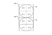
- FIG. 11G shows an example of the arrangement of photodiodes and color filters (RGB).
- RGB color filters
- two pixels 100-1 and 100-2 are shown.
- the arrangement relationship between the color of the color filter and the photodiode that generates the signal charge for obtaining the PA, PB, PC, and PD signals is expressed as “Color of color filter—PA, PB, PC, and PD signals. It was shown in the order of “photodiode that generates signal charge to obtain”. That is, an area indicated by “GA” is an area where a green (G) color filter is arranged and a photodiode 1 for generating a signal charge for outputting a PA signal is arranged. is there.
- a color filter of the same color is arranged in one row and two columns of the photodiode of one pixel 100.
- color filters of different colors are arranged in a Bayer arrangement for each of the two rows 100-1 and 100-2 in one row and two columns.
- each of the pixels 100-1 and 100-2 outputs a pixel signal as shown in FIG. 11C described above. This is because focus detection can be performed with high accuracy by performing focus detection using light incident on the photodiode via the same color filter. Furthermore, the form which performs a focus detection using the pixel signal which the some pixel 100 outputs may be sufficient.
- a digital A signal and a digital B signal obtained by converting a pixel signal of the pixel 100-1 and a pixel signal of the pixel 100-2, which are output from a photodiode included in an area where a green (G) color filter is arranged.
- the focus detection may be performed by detecting a phase difference from each combination of the converted digital C signal and digital D signal, and the digital A + B signal and digital C + D signal.
- a combination of any one of a digital A signal and a digital B signal, or a digital C signal and a digital D signal, and a combination of a digital A + B signal and a digital C + D signal may be used. .
- FIG. 11G shows a form in which focus detection is performed using the pixels 100-1 and 100-2 arranged in the horizontal direction (direction in which the HSC 14 scans).
- FIG. 11H shows an example of the arrangement of color filters when focus detection is performed using the pixels 100-1 and 100-2 arranged in the vertical direction (direction in which VSC2 scans).
- each of the pixels 100-1 and 100-2 preferably outputs a pixel signal as shown in FIG. 11C.
- at least the color filters arranged in the photoelectric conversion units adjacent to the pixel 100-1 and the pixel 100-2 may have the same color.
- the present embodiment has been described based on the form having the pixel 100 illustrated in FIG. 8A and the analog-digital conversion unit 16 of the first embodiment.
- an imaging apparatus having the pixel 100 illustrated in FIG. 8A and the analog-digital conversion unit 16 described in Embodiments 2 to 5 can be preferably implemented.
- the pixel 100 in FIG. 8A has four photodiodes, the number is not limited to this. In other words, any configuration having a plurality of photodiodes and a pixel 100 in which one microlens is arranged can be preferably implemented. Even in these forms, the effects described in each of the first to fourth embodiments can be obtained, and further, the focus detection by the phase difference detection method can be more suitably performed.
- Example An example in which the imaging apparatus described in Examples 1 to 4 is applied to an imaging system will be described.
- Examples of the imaging system include a digital still camera, a digital camcorder, and a surveillance camera.
- a schematic diagram when an imaging apparatus is applied to a digital still camera can be the same as FIG. 12 described in the fifth embodiment.
- the imaging system of the present embodiment can perform an imaging operation by applying the imaging device 154.
Landscapes
- Engineering & Computer Science (AREA)
- Multimedia (AREA)
- Signal Processing (AREA)
- Transforming Light Signals Into Electric Signals (AREA)
- Solid State Image Pick-Up Elements (AREA)
Abstract
Description
図1Aは、本実施例に関わる画素の等価回路の一例を示したものである。1、51は光電変換部である。本実施例では光電変換部はフォトダイオードである。20、50は転送MOSトランジスタ、4はリセットMOSトランジスタ、5は増幅MOSトランジスタ、6は選択MOSトランジスタである。フォトダイオード1、51では光電変換により、入射光に基づいた信号電荷が生じる。転送MOSトランジスタ20のゲートに、後述する垂直走査回路(図1Bにて、VSC(Vertical Scanning Circuit)と記載した)2が供給する転送パルスPTX1をHighレベル(以降、Hレベルと表記する。同様に、LowレベルをLレベルと表記する。)とすると、フォトダイオード1が保持する信号電荷が増幅MOSトランジスタ5のゲートに転送される。増幅MOSトランジスタ5のゲートは、すなわち増幅MOSトランジスタ5の制御電極である。同様に、転送MOSトランジスタ50のゲートに、同様に垂直走査回路2が供給する転送パルスPTX2をHレベルとすると、フォトダイオード51が保持する信号電荷が増幅MOSトランジスタ5のゲートに転送される。リセットMOSトランジスタ4のゲートに垂直走査回路2が供給するリセットパルスPRESをHレベルとすると、増幅MOSトランジスタ5のゲートの電位がリセットされる。増幅MOSトランジスタ5は、ゲートに転送された信号電荷に基づいて、電気信号を選択MOSトランジスタ6に出力する。選択MOSトランジスタ6は、増幅MOSトランジスタ5が出力した信号を、垂直走査回路2からゲートに供給される選択パルスPSELがHレベルの時に垂直信号線7に出力する。この画素100から垂直信号線7に出力される信号が先述した画素信号に相当する。各列の垂直信号線7には、電流源8から電流が供給されている。本実施例のアナログ信号出力部は画素100を含んで構成される。
図3Aは、本実施例の撮像装置の一例を示した等価回路図である。実施例1で説明した図1Bと同じ機能を有するものについては、図1Bで付した符号と同一の符号を付している。
図4Aは、本実施例の撮像装置の一例を示した等価回路図である。本実施例の撮像装置は、ラッチ選択回路12を設けず、画素の各列に対応してカウンタ制御回路16が設けられている。また、実施例1,2では第1のカウンタ18が各列のラッチ回路13に共通のカウント信号を与えていたが、本実施例では、第2のカウンタ19が各列のカウンタ制御回路16に対応して設けられている。そして、第2のカウンタ19の信号を保持するメモリ25が各列の第2のカウンタ19に対応して設けられている。第2のカウンタ19の信号を保持するメモリ25は、反転増幅器17が出力するGN信号に基づいて生成するデジタルN´信号を保持する第1の信号保持部である。さらにメモリ25は、第3の信号とランプ信号Vrampとの比較において、デジタルN´信号を第2のカウンタ19に出力する。カウンタ制御回路16は、不図示のタイミングジェネレータからクロックパルス信号clkが入力される。さらにカウンタ制御回路16は、カウント信号リセットパルスCNT Reset、パルスtranstom、パルスtranstocに基づいて、第2のカウンタ19、メモリ25を動作させる。Latch26は、第2のカウンタ19のカウント信号を保持する。実施例2では、第2の信号を変換したデジタル信号、第3の信号を変換したデジタル信号を保持する第2の信号保持部としてLatch_a13-1、Latch_b13-2の2つを有していたが、本実施例はLatch26の一つのみとすることができる。Latch26は、本実施例の第2の信号を変換したデジタル信号、第3の信号を変換したデジタル信号を保持する第2の信号保持部である。各列のLatch26にはラッチ信号LATが与えられ、ラッチ信号LATがHレベルの時に第2のカウンタ19が出力するカウント信号値を取り込む。ランプ信号発生回路10には、ランプ信号の電位を初期値にリセットするランプリセットパルスRamp Resetが供給される。
図6Aは本実施例の撮像装置の一例を示した等価回路図である。本実施例の撮像装置は、不図示のタイミングジェネレータからカウンタ制御回路16を介して第2のカウンタ19にモード設定パルスmodeが与えられる点が実施例3と異なっている。モード設定パルスmodeは、後述する第2のカウンタ19のモードを切り替えるためのパルスである。
本実施例は、撮像装置に設けられた画素100が出力する画素信号を用いて、位相差検出方式による焦点検出を行う形態である。
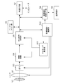
2 垂直走査回路
4 リセットMOSトランジスタ
5 増幅MOSトランジスタ
6 選択MOSトランジスタ
7 垂直信号線
8 電流源
9 比較器
10 ランプ発生回路
13 ラッチ回路
14 水平走査回路
15 差分信号出力部
16 アナログデジタル変換部
18 カウンタ
20,50 転送MOSトランジスタ
21 回路部
100 画素
Claims (17)
- アナログ信号出力部と、アナログデジタル変換部と、を含む撮像装置であって、
前記アナログ信号出力部は画素を含み、
前記画素は、光電変換部を有し、
前記アナログ信号出力部は、
前記アナログ信号出力部のノイズ信号である第1の信号と、
前記光電変換部で生成した信号電荷に基づく第2の信号と、
前記信号電荷に前記光電変換部で生成した別の信号電荷を加算した信号電荷に基づく第3の信号と、
をそれぞれ出力し、
前記アナログデジタル変換部は、前記第1、第2、第3の信号をそれぞれデジタル信号に変換し、
前記アナログデジタル変換部が、前記第1の信号を変換した前記デジタル信号を保持する信号保持部を有することを特徴とする撮像装置。 - 前記画素は少なくともn個(nは2以上の自然数)の光電変換部を有し、
前記アナログ信号出力部は、
前記n個の光電変換部のうちのm個(mはn>mの関係式を満たす自然数)の前記光電変換部で生成した信号電荷に基づく前記第2の信号と、
前記n個の光電変換部で生成した信号電荷に基づく前記第3の信号と、をそれぞれ出力することを特徴とする請求項1に記載の撮像装置。 - 前記アナログデジタル変換部が、
前記第2の信号を変換した前記デジタル信号と前記第1の信号を変換した前記デジタル信号との差分信号と、前記第3の信号を変換した前記デジタル信号と前記第1の信号を変換した前記デジタル信号との差分信号とを、同一の前記信号保持部が保持した、前記第1の信号を変換した前記デジタル信号によってそれぞれ生成することを特徴とする請求項2に記載の撮像装置。 - 前記撮像装置は、
マイクロレンズを複数有するマイクロレンズアレイをさらに有し、
1つの前記マイクロレンズは、前記画素の前記複数の光電変換部に光を集光させて入射させることを特徴とする請求項2または3に記載の撮像装置。 - 前記アナログデジタル変換部は比較器とカウンタとを有し、
前記比較器は、前記第1、第2、第3の信号の各々と時間に依存して電位が変化する参照信号とを比較したそれぞれの比較結果信号を出力し、
前記カウンタは、クロックパルス信号が供給され、前記クロックパルス信号を計数したカウント信号を出力し、
前記比較結果信号の信号値が変化したタイミングと、前記カウント信号とに基づいて、前記第1、第2、第3の信号を前記デジタル信号に変換することを特徴とする請求項1~4のいずれかに記載の撮像装置。 - 前記信号保持部は、前記参照信号の電位の時間に依存した変化を開始するタイミングから前記比較結果信号の信号値が変化したタイミングまでの前記カウント信号を保持することを特徴とする請求項5に記載の撮像装置。
- 前記アナログデジタル変換部は複数の回路部を有し、
複数の前記回路部の各々は前記比較器と前記信号保持部とを有し、
前記アナログ信号出力部を複数有し、
複数の前記アナログ信号出力部の各々と、複数の前記回路部の各々とが対応して設けられていることを特徴とする請求項5または6に記載の撮像装置。 - 前記第1の信号を変換した前記デジタル信号が、前記第1の信号と前記参照信号との前記比較結果信号の信号値が変化したタイミングから前記参照信号の電位の時間に依存した変化を終了するタイミングまでの前記カウント信号の信号値であり、
前記カウンタは、前記第2の信号と前記参照信号との比較と、前記第3の信号と前記参照信号との比較とにおいて、前記参照信号の電位の時間に依存した変化を開始するタイミングから前記比較結果信号の信号値が変化したタイミングまでの期間の計数を、前記信号保持部が前記カウンタに出力する、前記第1の信号を変換した前記デジタル信号の信号値から行うことを特徴とする請求項5~7のいずれかに記載の撮像装置。 - 前記アナログ信号出力部は増幅部を有し、
前記ノイズ信号と複数の前記信号のそれぞれは、前記画素が出力する信号を前記増幅部が増幅して出力した信号であることを特徴とする請求項1~9のいずれかに記載の撮像装置。 - 請求項4に記載の撮像装置と、
前記撮像装置に光を集光する光学系と、
前記撮像装置から、前記第2の信号を変換した前記デジタル信号と前記第1の信号を変換した前記デジタル信号との第1の差分信号と、前記第3の信号を変換した前記デジタル信号と前記第1の信号を変換した前記デジタル信号との第2の差分信号とが入力されるデジタル信号処理部と、を有する撮像システムであって、
前記デジタル信号処理部が、
前記第1の差分信号と前記第2の差分信号との差分である第3の差分信号を得て、前記第3の差分信号と、前記第1の差分信号とによって、焦点検出を行うことを特徴とする撮像システム。 - アナログ信号出力部と、アナログデジタル変換部と、を含む撮像装置の駆動方法であって、
前記アナログ信号出力部は画素を含み、
前記画素は、光電変換部を有し、
前記アナログ信号出力部は、
前記アナログ信号出力部のノイズ信号の第1の信号と、
前記光電変換部で生成した信号電荷に基づく第2の信号と、
前記信号電荷に前記光電変換部で生成した別の信号電荷を加算した信号電荷に基づく第3の信号と、をそれぞれ出力し、
前記アナログデジタル変換部が、前記第1、第2、第3の信号をデジタル信号に変換することを特徴とする撮像装置の駆動方法。 - 前記画素は、少なくともn個(nは2以上の自然数)の光電変換部を有し、
前記アナログ信号出力部が、
前記n個の光電変換部のうちのm個(mはn>mの関係式を満たす自然数)の前記光電変換部の生成した信号電荷に基づく前記第2の信号と、
前記n個の前記光電変換部の生成した信号電荷に基づく前記第3の信号と、をそれぞれ出力することを特徴とする請求項11に記載の撮像装置の駆動方法。 - 前記アナログ信号出力部が前記第1、第2、第3の信号を出力した後、
前記n個の光電変換部とは別のp個(pは自然数)の前記光電変換部の生成した信号電荷に基づく信号と、
前記p個よりも多く、前記n個の光電変換部とは別のq個(qは自然数)の前記光電変換部の生成した信号電荷に基づく信号と、を出力することを特徴とする請求項12に記載の撮像装置の駆動方法。 - 前記アナログデジタル変換部が、前記第2の信号を変換したデジタル信号と前記第1の信号を変換したデジタル信号との差分信号と、前記第3の信号を変換したデジタル信号と前記第1の信号を変換したデジタル信号との差分信号と、を前記第1の信号を変換した同一のデジタル信号によってそれぞれ生成することを特徴とする請求項11~13のいずれかに記載の撮像装置の駆動方法。
- 画素を含むアナログ信号出力部の複数と、前記アナログ信号出力部に対応して設けられたアナログデジタル変換部と、マイクロレンズを複数有するマイクロレンズアレイと、を有する撮像装置と、
前記撮像装置に光を集光する光学系と、
を有する撮像システムの駆動方法であって、
前記画素は、各々が1つの前記マイクロレンズに対応して設けられた、少なくともn個(nは2以上の自然数)の光電変換部の光電変換部を有し、
前記駆動方法は、
前記アナログ信号出力部が、
前記アナログ信号出力部のノイズ信号である第1の信号と、
前記n個の光電変換部のうちのm個(mはn>mの関係式を満たす自然数)の前記光電変換部の生成した信号電荷に基づく第2の信号と、
前記n個の光電変換部の生成した信号電荷に基づく第3の信号と、をそれぞれ出力し、
前記アナログデジタル変換部が、前記第1、第2、第3の信号をそれぞれデジタル信号に変換する工程と、
前記撮像装置が、前記第2の信号を変換したデジタル信号と前記第1の信号を変換したデジタル信号との第1の差分信号と、前記第3の信号を変換したデジタル信号と前記第1の信号を変換したデジタル信号との第2の差分信号とを、前記第1の信号を変換した同一のデジタル信号によってそれぞれ生成する第1の工程と、
前記第1の差分信号と前記第2の差分信号との差分である第3の差分信号を得て、
前記第3の差分信号と前記第1の差分信号とによって焦点検出を行う第2の工程と、を有することを特徴とする撮像システムの駆動方法。 - 前記撮像装置は、さらに複数の前記光電変換部の各々に各色が対応して設けられたカラーフィルタを有し、
前記第1の工程が、
前記第1の信号と、同色の前記カラーフィルタが設けられた前記n個および前記m個の光電変換部が生成した前記信号電荷に基づく前記第2、第3の信号と、に基づいて、前記第1の差分信号と前記第2の差分信号とを得る工程であることを特徴とする請求項15に記載の撮像システムの駆動方法。 - 前記第1の画素と前記第2の画素が有する前記n個の光電変換部に同色の前記カラーフィルタが配され、
前記第1の工程が、前記第1の画素と前記第2の画素の各々について、
前記第1、第2、第3の信号に基づいて前記第1の差分信号と前記第2の差分信号とを得る工程であり、
前記第2の工程が、前記第1の画素についての前記第3の差分信号を得て、
前記第1の画素についての前記第1の差分信号と前記第3の差分信号と、
前記第1の画素についての前記第2の差分信号と前記第2の画素についての前記第2の差分信号と、
に基づいて焦点検出を行う工程であることを特徴とする請求項16に記載の撮像システムの駆動方法。
Priority Applications (5)
| Application Number | Priority Date | Filing Date | Title |
|---|---|---|---|
| PCT/JP2012/054978 WO2013128581A1 (ja) | 2012-02-28 | 2012-02-28 | 撮像装置、撮像システム、撮像装置の駆動方法 |
| JP2014501885A JP6053750B2 (ja) | 2012-02-28 | 2012-02-28 | 撮像装置、撮像システム、撮像装置の駆動方法 |
| CN201280070803.3A CN104137535B (zh) | 2012-02-28 | 2012-02-28 | 成像装置、成像系统和成像装置的驱动方法 |
| GB1416579.9A GB2515927B (en) | 2012-02-28 | 2012-02-28 | Imaging device, imaging system and method for driving imaging device |
| US13/776,509 US9264642B2 (en) | 2012-02-28 | 2013-02-25 | Imaging device, imaging system, and method for driving imaging device for generating and converting signals based on photoelectric and noise |
Applications Claiming Priority (1)
| Application Number | Priority Date | Filing Date | Title |
|---|---|---|---|
| PCT/JP2012/054978 WO2013128581A1 (ja) | 2012-02-28 | 2012-02-28 | 撮像装置、撮像システム、撮像装置の駆動方法 |
Publications (2)
| Publication Number | Publication Date |
|---|---|
| WO2013128581A1 true WO2013128581A1 (ja) | 2013-09-06 |
| WO2013128581A9 WO2013128581A9 (ja) | 2014-09-04 |
Family
ID=49002492
Family Applications (1)
| Application Number | Title | Priority Date | Filing Date |
|---|---|---|---|
| PCT/JP2012/054978 Ceased WO2013128581A1 (ja) | 2012-02-28 | 2012-02-28 | 撮像装置、撮像システム、撮像装置の駆動方法 |
Country Status (5)
| Country | Link |
|---|---|
| US (1) | US9264642B2 (ja) |
| JP (1) | JP6053750B2 (ja) |
| CN (1) | CN104137535B (ja) |
| GB (1) | GB2515927B (ja) |
| WO (1) | WO2013128581A1 (ja) |
Cited By (8)
| Publication number | Priority date | Publication date | Assignee | Title |
|---|---|---|---|---|
| GB2507616A (en) * | 2012-07-31 | 2014-05-07 | Canon Kk | Image sensor with plural photodetectors sharing common amplifier and having different readout timings |
| JP2015056707A (ja) * | 2013-09-11 | 2015-03-23 | キヤノン株式会社 | 撮像装置およびその制御方法、撮像システム、プログラム、記憶媒体 |
| JP2015216625A (ja) * | 2014-04-22 | 2015-12-03 | キヤノン株式会社 | 撮像素子及び撮像装置 |
| JP2016131346A (ja) * | 2015-01-15 | 2016-07-21 | キヤノン株式会社 | 制御装置、撮像装置、制御方法、プログラム、記憶媒体 |
| JP2016144183A (ja) * | 2015-02-05 | 2016-08-08 | キヤノン株式会社 | 画像処理装置 |
| JP2018515995A (ja) * | 2015-05-12 | 2018-06-14 | ピグザリス | 取得速度が速いアナログデジタル変換を用いて、画素マトリクスを有するセンサを読み出すための回路、およびこのような回路を含む画像センサ |
| US10630929B2 (en) | 2017-12-01 | 2020-04-21 | Canon Kabushiki Kaisha | Solid-state imaging device and signal processing device |
| US10638066B2 (en) | 2018-02-05 | 2020-04-28 | Canon Kabushiki Kaisha | Imaging apparatus |
Families Citing this family (11)
| Publication number | Priority date | Publication date | Assignee | Title |
|---|---|---|---|---|
| US8742309B2 (en) | 2011-01-28 | 2014-06-03 | Aptina Imaging Corporation | Imagers with depth sensing capabilities |
| US10015471B2 (en) | 2011-08-12 | 2018-07-03 | Semiconductor Components Industries, Llc | Asymmetric angular response pixels for single sensor stereo |
| US9554115B2 (en) * | 2012-02-27 | 2017-01-24 | Semiconductor Components Industries, Llc | Imaging pixels with depth sensing capabilities |
| JP6480712B2 (ja) * | 2014-02-06 | 2019-03-13 | キヤノン株式会社 | 撮像装置及びその制御方法 |
| US9445018B2 (en) * | 2014-05-01 | 2016-09-13 | Semiconductor Components Industries, Llc | Imaging systems with phase detection pixels |
| US9888198B2 (en) | 2014-06-03 | 2018-02-06 | Semiconductor Components Industries, Llc | Imaging systems having image sensor pixel arrays with sub-pixel resolution capabilities |
| US9749556B2 (en) | 2015-03-24 | 2017-08-29 | Semiconductor Components Industries, Llc | Imaging systems having image sensor pixel arrays with phase detection capabilities |
| EP3119081B1 (en) * | 2015-07-16 | 2018-09-19 | Canon Kabushiki Kaisha | Imaging apparatus and imaging system |
| JP6746301B2 (ja) | 2015-11-30 | 2020-08-26 | キヤノン株式会社 | 撮像装置の駆動方法、撮像装置、撮像システム |
| US10015429B2 (en) * | 2015-12-30 | 2018-07-03 | Omnivision Technologies, Inc. | Method and system for reducing noise in an image sensor using a parallel multi-ramps merged comparator analog-to-digital converter |
| US10506318B2 (en) * | 2016-02-23 | 2019-12-10 | Infineon Technologies Ag | System and method for signal read-out using source follower feedback |
Citations (5)
| Publication number | Priority date | Publication date | Assignee | Title |
|---|---|---|---|---|
| JP2004134867A (ja) * | 2002-10-08 | 2004-04-30 | Canon Inc | 固体撮像装置、その駆動方法、及び撮像システム |
| JP2011217206A (ja) * | 2010-03-31 | 2011-10-27 | Honda Motor Co Ltd | 固体撮像装置 |
| JP2011223270A (ja) * | 2010-04-08 | 2011-11-04 | Toshiba Corp | 固体撮像装置およびその制御動作 |
| JP2011259485A (ja) * | 2011-08-08 | 2011-12-22 | Sony Corp | 固体撮像装置、撮像装置、ad変換ゲイン調整方法 |
| JP2012039386A (ja) * | 2010-08-06 | 2012-02-23 | Olympus Corp | 時間検出回路、ad変換器、および固体撮像装置 |
Family Cites Families (6)
| Publication number | Priority date | Publication date | Assignee | Title |
|---|---|---|---|---|
| US4195360A (en) * | 1973-10-16 | 1980-03-25 | Her Majesty The Queen In Right Of Canada, As Represented By The Minister Of National Defence | Signal processing circuit |
| US6021172A (en) * | 1994-01-28 | 2000-02-01 | California Institute Of Technology | Active pixel sensor having intra-pixel charge transfer with analog-to-digital converter |
| JP2007074447A (ja) * | 2005-09-07 | 2007-03-22 | Fujitsu Ltd | Cmosセンサ |
| TWI504256B (zh) * | 2008-04-07 | 2015-10-11 | Sony Corp | 固態成像裝置,其訊號處理方法,及電子設備 |
| JP4693863B2 (ja) * | 2008-04-30 | 2011-06-01 | キヤノン株式会社 | 固体撮像装置及び固体撮像装置の駆動方法 |
| JP5489641B2 (ja) * | 2008-11-11 | 2014-05-14 | キヤノン株式会社 | 焦点検出装置及びその制御方法 |
-
2012
- 2012-02-28 GB GB1416579.9A patent/GB2515927B/en active Active
- 2012-02-28 CN CN201280070803.3A patent/CN104137535B/zh active Active
- 2012-02-28 WO PCT/JP2012/054978 patent/WO2013128581A1/ja not_active Ceased
- 2012-02-28 JP JP2014501885A patent/JP6053750B2/ja active Active
-
2013
- 2013-02-25 US US13/776,509 patent/US9264642B2/en active Active
Patent Citations (5)
| Publication number | Priority date | Publication date | Assignee | Title |
|---|---|---|---|---|
| JP2004134867A (ja) * | 2002-10-08 | 2004-04-30 | Canon Inc | 固体撮像装置、その駆動方法、及び撮像システム |
| JP2011217206A (ja) * | 2010-03-31 | 2011-10-27 | Honda Motor Co Ltd | 固体撮像装置 |
| JP2011223270A (ja) * | 2010-04-08 | 2011-11-04 | Toshiba Corp | 固体撮像装置およびその制御動作 |
| JP2012039386A (ja) * | 2010-08-06 | 2012-02-23 | Olympus Corp | 時間検出回路、ad変換器、および固体撮像装置 |
| JP2011259485A (ja) * | 2011-08-08 | 2011-12-22 | Sony Corp | 固体撮像装置、撮像装置、ad変換ゲイン調整方法 |
Cited By (10)
| Publication number | Priority date | Publication date | Assignee | Title |
|---|---|---|---|---|
| GB2507616A (en) * | 2012-07-31 | 2014-05-07 | Canon Kk | Image sensor with plural photodetectors sharing common amplifier and having different readout timings |
| GB2507616B (en) * | 2012-07-31 | 2015-09-09 | Canon Kk | Solid-state image sensor, camera, and method of driving solid-state sensor |
| US9232164B2 (en) | 2012-07-31 | 2016-01-05 | Canon Kabushiki Kaisha | Solid-state image sensor, camera, and method of driving solid-state image sensor |
| JP2015056707A (ja) * | 2013-09-11 | 2015-03-23 | キヤノン株式会社 | 撮像装置およびその制御方法、撮像システム、プログラム、記憶媒体 |
| JP2015216625A (ja) * | 2014-04-22 | 2015-12-03 | キヤノン株式会社 | 撮像素子及び撮像装置 |
| JP2016131346A (ja) * | 2015-01-15 | 2016-07-21 | キヤノン株式会社 | 制御装置、撮像装置、制御方法、プログラム、記憶媒体 |
| JP2016144183A (ja) * | 2015-02-05 | 2016-08-08 | キヤノン株式会社 | 画像処理装置 |
| JP2018515995A (ja) * | 2015-05-12 | 2018-06-14 | ピグザリス | 取得速度が速いアナログデジタル変換を用いて、画素マトリクスを有するセンサを読み出すための回路、およびこのような回路を含む画像センサ |
| US10630929B2 (en) | 2017-12-01 | 2020-04-21 | Canon Kabushiki Kaisha | Solid-state imaging device and signal processing device |
| US10638066B2 (en) | 2018-02-05 | 2020-04-28 | Canon Kabushiki Kaisha | Imaging apparatus |
Also Published As
| Publication number | Publication date |
|---|---|
| GB201416579D0 (en) | 2014-11-05 |
| WO2013128581A9 (ja) | 2014-09-04 |
| US9264642B2 (en) | 2016-02-16 |
| GB2515927A (en) | 2015-01-07 |
| GB2515927B (en) | 2019-05-01 |
| JP6053750B2 (ja) | 2016-12-27 |
| US20130222662A1 (en) | 2013-08-29 |
| JPWO2013128581A1 (ja) | 2015-07-30 |
| CN104137535A (zh) | 2014-11-05 |
| CN104137535B (zh) | 2017-11-28 |
Similar Documents
| Publication | Publication Date | Title |
|---|---|---|
| JP6053750B2 (ja) | 撮像装置、撮像システム、撮像装置の駆動方法 | |
| JP6164846B2 (ja) | 撮像装置、撮像システム、撮像装置の駆動方法 | |
| JP6041500B2 (ja) | 撮像装置、撮像システム、撮像装置の駆動方法、撮像システムの駆動方法 | |
| JP5886806B2 (ja) | 固体撮像装置 | |
| US9185313B2 (en) | Solid-state imaging device, method of driving the same, signal processing method for the same, and imaging apparatus | |
| US9232165B2 (en) | Solid-state imaging apparatus and method for driving solid-state imaging apparatus | |
| US8269872B2 (en) | Analog-to-digital converter, analog-to-digital converting method, solid-state image pickup device, and camera system | |
| US8004587B2 (en) | Solid-state imaging device, signal processing method for the same, and imaging apparatus | |
| US20100091167A1 (en) | Solid-state image sensor and camera system | |
| US20150092097A1 (en) | Imaging apparatus | |
| US9332204B2 (en) | AD conversion circuit and solid-state imaging device | |
| US20180139399A1 (en) | Ad converter, signal processing method, solid-state imaging device, and electronic apparatus | |
| JP2013251874A (ja) | 撮像装置、撮像装置の駆動方法、撮像システム、撮像システムの駆動方法 | |
| JP6173058B2 (ja) | 撮像装置、撮像システム、撮像装置の駆動方法、撮像システムの駆動方法 | |
| JP2017147700A (ja) | 撮像装置、撮像システム、撮像装置の駆動方法 | |
| JP2013143636A (ja) | 固体撮像装置、固体撮像装置の信号処理方法、及び、電子機器 | |
| JP6598837B2 (ja) | 撮像装置、撮像システム | |
| JP6242467B2 (ja) | 撮像装置、撮像システム | |
| US20130342744A1 (en) | Solid-state imaging device, method of driving the same, and electronic apparatus | |
| US9906750B2 (en) | Image pickup device driving method, image pickup device, and image pickup system using reset cancellation | |
| JP2013141144A (ja) | A/d変換回路、撮像素子、および電子機器 | |
| JP2013197866A (ja) | 個体撮像装置および駆動方法、並びに、電子機器 |
Legal Events
| Date | Code | Title | Description |
|---|---|---|---|
| 121 | Ep: the epo has been informed by wipo that ep was designated in this application |
Ref document number: 12869647 Country of ref document: EP Kind code of ref document: A1 |
|
| ENP | Entry into the national phase |
Ref document number: 2014501885 Country of ref document: JP Kind code of ref document: A |
|
| NENP | Non-entry into the national phase |
Ref country code: DE |
|
| ENP | Entry into the national phase |
Ref document number: 1416579 Country of ref document: GB Kind code of ref document: A Free format text: PCT FILING DATE = 20120228 |
|
| WWE | Wipo information: entry into national phase |
Ref document number: 1416579.9 Country of ref document: GB |
|
| 122 | Ep: pct application non-entry in european phase |
Ref document number: 12869647 Country of ref document: EP Kind code of ref document: A1 |