WO2013125698A1 - レーザ走査型撮影装置 - Google Patents
レーザ走査型撮影装置 Download PDFInfo
- Publication number
- WO2013125698A1 WO2013125698A1 PCT/JP2013/054584 JP2013054584W WO2013125698A1 WO 2013125698 A1 WO2013125698 A1 WO 2013125698A1 JP 2013054584 W JP2013054584 W JP 2013054584W WO 2013125698 A1 WO2013125698 A1 WO 2013125698A1
- Authority
- WO
- WIPO (PCT)
- Prior art keywords
- scanning
- timing signal
- resonant scanner
- speed signal
- image
- Prior art date
- Legal status (The legal status is an assumption and is not a legal conclusion. Google has not performed a legal analysis and makes no representation as to the accuracy of the status listed.)
- Ceased
Links
Images





Classifications
-
- A—HUMAN NECESSITIES
- A61—MEDICAL OR VETERINARY SCIENCE; HYGIENE
- A61B—DIAGNOSIS; SURGERY; IDENTIFICATION
- A61B3/00—Apparatus for testing the eyes; Instruments for examining the eyes
- A61B3/10—Objective types, i.e. instruments for examining the eyes independent of the patients' perceptions or reactions
- A61B3/1025—Objective types, i.e. instruments for examining the eyes independent of the patients' perceptions or reactions for confocal scanning
Definitions
- the present invention relates to a laser scanning type photographing apparatus that constructs a photographed image of an object to be imaged by scanning the object to be imaged with laser light and receiving reflected light reflected from the object to be imaged.
- a confocal laser scanning ophthalmoscope (SLO: Scanning ⁇ ⁇ ⁇ La Ophthalmoscope) is known as an ophthalmologic photographing apparatus using laser scanning technology (see Patent Document 1).
- Such a confocal laser scanning ophthalmoscope has a scanning illumination optical system that scans laser light toward an imaging target portion, and a light receiving optical system that receives reflected light reflected from the imaging target portion, A timing signal is output each time the scanning means of the scanning illumination optical system reciprocates and scans the laser light, and the forward path when the laser light is scanned forward from the light reception signal of the light receiving sensor of the light receiving optical system based on this timing signal.
- a scan image and a return scan image when the laser beam is scanned backward are constructed, and a frame image is constructed by the forward scan image and the return scan image.
- a resonance type scanner is used to scan a laser beam at a high speed, and a driver of the resonance type scanner outputs a timing signal according to a reciprocating scan of the laser beam.
- the resonance frequency of the scanner fluctuates about 80 ppm / ° C. with respect to the environmental temperature change.
- the period until the end of the forward scan image and the period until the start of the return scan image are set with reference to the timing signal so that the end of the forward scan image and the start end of the return scan image coincide with each other.
- the resonance frequency of the scanner fluctuates, there is a problem that the end of the forward scan image does not coincide with the start of the return scan image, and the image quality of the frame image is degraded.
- An object of the present invention is to provide a laser scanning type photographing apparatus capable of obtaining a high-quality frame image regardless of environmental temperature changes.
- a laser scanning imaging apparatus includes a laser beam generator that emits imaging laser light, a scanning illumination optical system that illuminates the imaging target unit by scanning the laser beam onto the imaging target unit, A light receiving optical system that receives the reflected light reflected from the object to be imaged, and the scanning illumination optical system includes a scanning device that reciprocally scans the laser light in a predetermined direction. The scanning device reciprocates the laser light.
- a timing signal is output in response to scanning, and the forward scanning image obtained by the scanning device scanning the laser beam in the forward direction from the light receiving signal of the light receiving unit of the light receiving optical system based on the timing signal, and the laser A laser scanning imaging apparatus that constructs a frame image based on a backward scanning image obtained by scanning light backward, The period at which the timing signal is output is measured, and based on the measured period of the timing signal, the scanning end of the forward scanning range for forming the forward scanning image and the backward scanning range for forming the backward scanning image are measured.
- An arithmetic and control unit is provided that constructs the frame image by matching the scanning start end with the scanning direction.
- a high-quality frame image can be obtained regardless of environmental temperature changes.
- FIG. 1 is an optical arrangement diagram showing a configuration of an optical system of a confocal laser scanning ophthalmoscope according to the present invention. It is the block diagram which showed the structure of the control system of the confocal laser scanning ophthalmoscope shown in FIG. It is the block diagram which showed the structure of the principal part of the arithmetic and control unit shown in FIG. It is a time chart which showed operation of a confocal laser scanning type ophthalmoscope. It is the time chart which showed the conventional operation
- reference numeral 10 denotes an optical system of a confocal laser scanning ophthalmoscope as a laser scanning imaging apparatus.
- the confocal laser scanning ophthalmoscope 10 scans a laser beam generator (laser beam generator) 11 that generates a laser beam for imaging, and a laser beam toward the fundus (an imaging target portion) Er of the eye E to be examined.
- a scanning illumination optical system 20 that illuminates and a light receiving optical system 40 that receives reflected light reflected from the fundus Er.
- the scanning illumination optical system 20 includes a collimating lens 22 that condenses the laser light generated from the laser light generator 11, a polarizing plate 23 that transmits only the P-polarized light of the laser light, a beam splitter 24, and the laser light up and down.
- a resonance scanner (resonant scanner) 25 that is a scanning device that performs reciprocal scanning, a scanner 26 that horizontally scans P-polarized laser light that is reciprocated up and down, a half-wave plate 27, a relay lens 28, and the like , A reflecting mirror 30, a focusing lens 31, and an objective lens 32.
- the half-wave plate 27 is for eliminating luminance unevenness.
- the half-wave plate 27 is rotated by a predetermined angle every time one frame is shot, and the brightness is obtained by synthesizing shot images until the rotation angle reaches 180 degrees. An image with little unevenness is obtained.
- the rotation axis 27a of the half-wave plate 27 is inclined with respect to the optical axis in order to prevent the reflected light reflected by the surface of the half-wave plate 27 from entering the light receiving sensor 44 described later. is there.
- the light receiving optical system 40 includes an objective lens 32, a focusing lens 31, a reflection mirror 30, a relay lens 28, a half-wave plate 27, a scanner 26, a resonant scanner 25, a beam splitter 24, and an S A polarizing plate 41 that transmits polarized reflected laser light, a relay lens 42, a confocal stop 43, and a light receiving sensor (light receiving unit) 44 are provided.
- FIG. 2 is a block diagram showing the configuration of the control system of the confocal laser scanning ophthalmoscope.
- reference numeral 50 denotes a driver circuit that drives the resonant scanner 25.
- the resonant scanner 25 outputs a speed signal Vm having a frequency corresponding to the vibration speed (resonance speed) of the mirror that scans the laser beam.
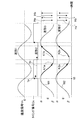
- the driver circuit 50 In addition to driving the resonant scanner 25, the driver circuit 50 generates a sinusoidal speed signal Vs (see FIG. 3) based on the speed signal Vm, and a timing signal Ds (FIG. 3) based on the speed signal Vs. Reference) is generated and output.
- Reference numeral 51 denotes a driver circuit that drives the scanner 26, and drives the scanner 26 based on an analog signal output from the D / A converter 52.
- the D / A converter 52 converts a digital scanner drive command signal output from an arithmetic control device 55 described later into an analog signal.
- 53 is a light receiving circuit that amplifies the light receiving signal of the light receiving sensor 44
- 54 is an A / D converter
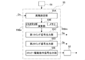
- 55 is an arithmetic control unit having a period measuring unit 55A (see FIG. 2A) for obtaining a period T at which the timing signal Ds is output. is there.
- the arithmetic and control unit 55 based on the period T obtained by the period measuring unit 55A, performs a time t1 when the deflection angle of the resonant scanner 25 becomes “ ⁇ ” during the forward scanning of the laser light (FIG. 2A). 3), the deflection angle of the resonant scanner 25 (scanning end deflection angle) ⁇ (see FIG. 2A).
- a scanner drive command signal output unit 55E for outputting a scanner drive command signal for moving the image, and a frame image is stored in an image memory 57 (to be described later) from the digital received light signal converted by the A / D converter 54. Or build.
- the calculation unit 55B is, for example, a graph M1 showing the deflection angle of the resonant scanner 25 (see FIG. 3), that is, the phase is delayed by 90 degrees with respect to the sine wave of the speed signal Vs.
- 56 is a main clock signal generator for outputting a main clock signal
- 57 is an image memory for constructing a frame image
- 58 is an image constructed in the memory, and displays or constructs an image on a display unit (not shown).
- It is a personal computer (personal computer) that stores images.
- the deflection angle ⁇ of the resonant scanner 25 is set in advance. [Operation] Next, the operation of the confocal laser scanning ophthalmoscope 10 configured as described above will be described.
- the laser beam generated by the laser beam generator 11 is condensed by the collimator lens 22 to be converted into a parallel beam, and only the P-polarized light is transmitted through the polarizing plate 23 in the laser beam that has become the parallel beam.
- the light passes through the beam splitter 24 and reaches the resonant scanner 25.
- the resonant scanner 25 is driven by the driver circuit 50 and resonates.
- the resonant scanner 25 reciprocally scans the P-polarized laser beam in the vertical direction by resonance vibration.
- the P-polarized laser light that has been reciprocally scanned in the vertical direction is scanned in the horizontal direction by the scanner 26 by the operation of the driver circuit 51, whereby the P-polarized laser light is scanned in a two-dimensional direction.
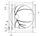
- the P-polarized laser light reaches the fundus Er of the eye E through the half-wave plate 27, the relay lens 28, the reflection mirror 30, the focusing lens 31, and the objective lens 32, and this fundus Er is shown in FIG. As shown in FIG.
- the laser reflected light reflected from the fundus Er contains P and S components due to the fibers of the retina. This reflected light reaches the beam splitter 24 through the objective lens 32, the focusing lens 31, the reflecting mirror 30, the relay lens 28, the half-wave plate 27, the scanner 26, and the resonant scanner 25.
- the laser reflected light that has reached the beam splitter 24 is reflected here and reaches the polarizing plate 41, where only the S-polarized laser reflected light passes through the polarizing plate 41 and passes through the relay lens 42 and the confocal stop 43.
- the light receiving sensor 44 receives the light.
- the reflected light reflected from other than the fundus Er becomes P-polarized reflected light by being irradiated with the P-polarized laser light, so that it is not received by the light receiving sensor 44 by the polarizing plate 41. For this reason, only the S-polarized light reflected by the fundus Er is received by the light receiving sensor 44.
- the light receiving sensor 44 outputs a light receiving signal corresponding to the amount of reflected light of S-polarized light, and the light receiving circuit 53 amplifies the light receiving signal.
- the amplified received light signal is A / D converted by the A / D converter 54 and taken into the arithmetic and control unit 55.
- the driver circuit 50 generates a sinusoidal speed signal Vs based on the speed signal Vm as shown in FIG. 3, and generates and outputs a timing signal Ds based on the speed signal Vs.
- the timing signal Ds becomes H level when the speed signal Vs changes from positive to negative (zero cross), and becomes L level when the speed signal Vs exceeds a predetermined positive threshold value.
- the period measurement unit 55A of the arithmetic control device 55 obtains the period T of the timing signal Ds, and the sine wave calculation unit 55Ba of the calculation unit 55B is delayed by 90 degrees with respect to the sine wave of the speed signal Vs based on the period T. Further, a graph M1 shown in FIG. 3 which is a sine wave waveform indicating the deflection angle of the resonant scanner 25 is obtained. This graph M1 is stored in the memory 55Bm.
- the calculation unit 55B of the calculation control device 55 has the deflection angle of the resonant scanner 25 “with reference to the time point t0 when the timing signal Ds is output, as shown in FIG.
- the time point “ ⁇ ” (outward scanning disclosure time point: scanning start end) t1 is obtained from the graph M1 stored in the memory 55Bm.
- the deflection angle ⁇ of the resonant scanner 25 is a deflection angle at which the construction of the forward scan image is started.
- the calculation unit 55B of the calculation control device 55 obtains a time point t2 at which the forward scan image is scanned (end time of the backward scan time) t2 from the graph M1 stored in the memory 55Bm.
- This time point t2 is a time point when the number of timing signals Ga output from the time point t1 becomes “N”, and “N” is the number of pixels in the scanning direction of the resonant scanner 25 of the image displayed on the display screen.
- the calculation unit 55B of the calculation control device 55 obtains the deflection angle ⁇ of the resonant scanner 25 at the time point t2 from the graph M1, and at the time when the deflection angle of the resonant scanner 25 becomes “ ⁇ ” during the backward scanning (return scanning start). Time) t3 is obtained from the graph M1.
- the calculation unit 55B of the calculation control device 55 includes the time t1 when the deflection angle of the resonant scanner 25 becomes “ ⁇ ”, the scanning end point t2 of the forward scanning image, and the deflection angle of the resonant scanner 25 at the scanning end point t2. ⁇ and the time point t3 when the deflection angle of the resonant scanner 25 during the backward scan becomes “ ⁇ ” are obtained.
- the time points t1, t2, and t3 obtained by the calculation unit 55B of the calculation control device 55 are stored in a memory (not shown).
- the first timing signal output unit 55C of the arithmetic and control unit 55 counts the time from the time t0 with the time when the timing signal Ds of the next cycle is output as t0, and when this time reaches the time t1.
- the output of the timing signal Ga is started.
- the timing signal Ga is output at a timing determined in advance based on the measured period T and the main clock signal output from the main clock signal generator 56.
- the arithmetic and control unit 55 sequentially designates an address for storing the received light reception signal in the image memory 57.
- the image memory 57 sequentially stores the received light signal taken in by the arithmetic and control unit 55 at a designated address.
- the first timing signal output unit 55C of the arithmetic and control unit 55 stops the output when the number of output timing signals Ga reaches a predetermined number N. Due to the stop of the output of the timing signal Ga, the image memory 57 does not store the light reception signal from this time t2.
- the data of the light reception signal captured during the period from the time point t1 to the time point t2 is the data of the light reception signal captured during the scanning period (forward scanning period) until the resonant scanner 25 rotates from the angle ⁇ to the angle ⁇ . Is stored in the image memory 57 as one forward scan image data.
- the image data of the forward scanning range Ha of the resonant scanner 25 is stored in the image memory 57 as one forward scanning image.
- the first timing signal output unit 55C of the arithmetic control device 55 outputs the timing signal Ga again at the timing obtained in advance when the timed time reaches the time point t3, and the image memory 57 is similar to the above in the arithmetic control device.
- the received light signal 55 is sequentially stored.
- the deflection angle of the resonant scanner 25 is ⁇ .
- the arithmetic and control unit 55 stops the output when the output number of the timing signal Ga reaches the predetermined number N, and the image memory 57 does not store the light reception signal (time t4: return scan end time).
- the data of the received light signal taken in the scanning period until the resonant scanner 25 rotates from the angle ⁇ to the angle ⁇ (period from the time point t3 to the time point t4: the backward scanning period) is stored in the memory 57 as one backward scanning image data.
- the image data of the backward scanning range Hb of the resonant scanner 25 is stored in the memory 57 as one backward scanning image.
- the forward scanning range Ha and the backward scanning range Hb coincide with each other in the scanning direction, and the scanning end of the forward scanning image and the backward scanning image. Is coincident with the deflection angle ⁇ of the resonant scanner 25. That is, the scanning end J1a of the forward scanning range of the resonant scanner 25 and the scanning starting end J1b of the backward scanning range coincide with each other in the scanning direction.
- the resonant frequency of the resonant scanner 25 is changed due to environmental changes, for example, when the resonant frequency is lowered, the period of generation of the timing signal Ds becomes longer due to the lowered resonant frequency.
- the graph indicating the deflection angle of the resonant scanner 25 is a graph M2 having a slightly longer period than the graph M1 in accordance with the decrease in the resonance frequency.
- This graph M2 is stored in the memory 55Bm.
- the graph M2 is obtained by the sine wave calculation unit 55Ba of the calculation unit 55B based on the cycle of the timing signal Ds in the same manner as described above.
- the arithmetic and control unit 55 determines that the time t1 when the deflection angle of the resonant scanner 25 becomes “ ⁇ ” (actually a time slightly longer than the time between the time t0 and the time t1 due to the longer period).
- the timing signal Ga is output at the timing obtained in advance, and the received light reception signals are sequentially stored in the image memory 57.
- the output number of the timing signal Ga reaches the predetermined number N, the output is stopped (time t2), and the memory 57 stops storing the received light signal.
- the calculation unit 55B of the calculation control device 55 obtains in advance the deflection angle of the resonant scanner 25 at time t2 from the graph M2. Since the period of the graph M2 is slightly longer than that of the graph M1, the deflection angle of the resonant scanner 25 at the time point t2 is “ ⁇ ′” that is slightly smaller than “ ⁇ ” in absolute value.
- the light reception signal data captured during the period from the time point t1 to the time point t2 is data of the light reception signal captured during the scanning period (outward scanning period) until the resonant scanner 25 rotates from the angle ⁇ to the angle ⁇ ′.
- the received light signal data captured during this forward scan period is the forward scan image data of the forward scan range Ha ′ (Ha> Ha ′) of the resonant scanner 25 as shown on the right side of the graph M2 in FIG. 3 and FIG. 1 is stored in the image memory 57 as a forward scan image.
- the scanning end of this one forward scanning image is when the deflection angle of the resonant scanner 25 is ⁇ ′.
- the calculation unit 55B of the calculation control device 55 obtains in advance a time point t3 ′ at which the deflection angle of the resonant scanner 25 becomes ⁇ ′.
- the arithmetic and control unit 55 outputs the timing signal Ga at the timing determined in advance at the time point t3 ′, and the image memory 57 sequentially stores the received light signals taken in by the arithmetic and control unit 55 in the same manner as described above. Go.
- the arithmetic and control unit 55 stops the output of the timing signal Ga when the output number becomes N, and the image memory 57 stops storing the received light signal (time t4 ′).
- the deflection angle of the resonant scanner 25 is “ ⁇ ”.
- the data of the received light signal acquired during the scanning period (return scan period) until the resonant scanner 25 rotates from the angle ⁇ ′ to the angle ⁇ is the return scan image data, and is stored in the memory 57 as one return scan image. Then, the scanning start end of the backward scanning image is when the deflection angle of the resonant scanner 25 is ⁇ ′.
- the forward scanning range Ha ′ and the backward scanning range Hb ′ are in the scanning direction.
- the scanning end of one forward scanning image and the scanning starting end of one backward scanning image coincide with each other at the deflection angle ⁇ ′ of the resonant scanner 25.
- the scanning end J2a of the forward scanning range Ha ′ and the scanning start end J2b of the backward scanning range Hb ′ of the resonant scanner 25 coincide with the deflection angle ⁇ ′, that is, the scanning direction. Therefore, a high-quality frame image can be obtained. This is because even if the resonant frequency of the resonant scanner 25 increases, the scanning end of the forward scanning range and the scanning start end of the backward scanning range coincide with the scanning direction, and a high-quality frame image can be obtained.
- the scanning end K2a of the forward scanning range Ha ′′ and the scanning start end K2b of the backward scanning range Hb ′′ of the resonant scanner 25 do not coincide with the scanning direction.
- the forward scanning range Ha ′′ and the backward scanning range Hb ′′ of the resonant scanner 25 are shown on the right side of the graph M2 in FIG. It deviates to the sea urchin up-and-down direction. That is, the scanning end of the forward scanning image and the scanning starting end of the backward scanning image are shifted, and the image quality of the frame image is degraded.
- the graph M1 is obtained from the timing signal Ds.
- the use range ( ⁇ to ⁇ ) of the deflection angle of the resonant scanner 25 is set, and this use range ( ⁇ to ⁇ ) to obtain time points t1 to t4 based on the period T of the timing signal Ds by an arithmetic expression for obtaining the graph M1, and obtain it in the forward scanning range from time point (forward scanning start time) t1 to time point (forward scanning end time) t2.
- a frame image may be constructed from the forward scan image obtained and the return scan image obtained in the return scan range from the time point (return scan start time) t3 to the time point (return scan end time) t4.
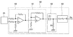
- FIG. 5 shows the configuration of the driver circuit 50.
- the driver circuit 50 is an operational amplifier (speed signal generating circuit) that generates a speed signal Vm output from the resonant scanner 25 into a sinusoidal speed signal Vs. ) 60, an amplifier 61 that amplifies the speed signal Vs, a high-pass filter 62 that removes low-frequency components from the speed signal Vs output from the amplifier 61, and a timing signal Ds (from the speed signal Vs that has passed through the high-pass filter 62.
- a comparator (timing signal generation circuit) 63 for generating a signal (see FIG. 3).
- the high pass filter 62 is composed of a resistor R1 and a capacitor C1, and cuts frequencies below a predetermined value.
- the speed signal Vs passes through the high-pass filter 62. Therefore, when the resistance value of the resistor R1 and the capacitance of the capacitor C1 change due to temperature change, the speed signal Vs with respect to the resonance waveform (graph M1 in FIG. 3) of the resonant scanner 25. As a result, the end of the forward scanning of the resonant scanner 25 does not match the start of the backward scanning, and the image quality of the frame image is degraded.
- the temperature characteristic of the resistor R1 and the temperature characteristic of the capacitor C1 are set to be opposite to each other to prevent a phase shift due to a temperature change.
- a capacitor C1 having a negative temperature characteristic is employed to correct the temperature characteristic of the resistor R1. Accordingly, it is possible to prevent a phase shift between the resonance waveform of the resonant scanner 25 and the waveform of the speed signal Vs with respect to a temperature change, and it is possible to prevent deterioration of the image quality of the frame image.
- FIG. 6 is a block diagram showing the configuration of the control system of the confocal laser scanning ophthalmoscope of the third embodiment.
- the confocal laser scanning ophthalmoscope driver circuit 150 holds the peak values Va and Vb of the speed signal Vs output from the operational amplifier 60 in addition to a drive circuit (not shown) for driving the resonant scanner 25.
- the peak hold circuit 101 always holds the peak values Va and Vb of the speed signal Vs, and obtains the intermediate value Vd from the average value of the maximum value Va and the minimum value Vb.
- the binarization processing circuit 102 uses the intermediate value Vd as a threshold value to make an H level signal when the voltage of the speed signal Vs is equal to or higher than the intermediate value Vd, and when the voltage of the speed signal Vs is smaller than the intermediate value Vd.
- the signal is processed into an L level signal. This binarization process cuts the direct current component of the speed signal Vs.
- the zero-cross detection circuit 103 outputs a zero-cross pulse Zp at the time of rising and falling because the speed signal Vs is zero-crossed when the H level signal rises and falls.
- reference numeral 155 denotes an arithmetic and control unit.
- the arithmetic and control unit 155 obtains the output cycle of the zero cross pulse Zp output from the zero cross detection circuit 103, and the deflection angle of the resonant scanner 25 is determined based on this output cycle.
- the time t1 when “ ⁇ ” is reached, the time t2 when the scanning of the forward scanning image is finished, the deflection angle ⁇ of the resonant scanner 25 at this time t2, and the deflection angle of the resonant scanner 25 during the backward scanning are “ ⁇ ”.
- the time t3 is obtained, and the same operation as that of the arithmetic and control unit 55 of the first embodiment is performed to construct a frame image in the memory 57.
- the DC component of the speed signal Vs changes, the DC component is cut by the binarization process, so that the zero cross position of the speed signal Vs can be accurately detected. Further, since a high-pass filter for removing a direct current component is not used, the generation time of the zero cross pulse Zp is not shifted from the resonance waveform (graph M1 in FIG. 3) of the resonant scanner 25 due to temperature change. For this reason, it is possible to prevent deterioration of the image quality of the frame image.
- the confocal laser scanning ophthalmoscope has been described.
- the present invention is not limited to this, and other laser scanning imaging apparatuses may be used.
Landscapes
- Life Sciences & Earth Sciences (AREA)
- Health & Medical Sciences (AREA)
- Medical Informatics (AREA)
- Biophysics (AREA)
- Ophthalmology & Optometry (AREA)
- Engineering & Computer Science (AREA)
- Biomedical Technology (AREA)
- Heart & Thoracic Surgery (AREA)
- Physics & Mathematics (AREA)
- Molecular Biology (AREA)
- Surgery (AREA)
- Animal Behavior & Ethology (AREA)
- General Health & Medical Sciences (AREA)
- Public Health (AREA)
- Veterinary Medicine (AREA)
- Mechanical Optical Scanning Systems (AREA)
- Microscoopes, Condenser (AREA)
- Eye Examination Apparatus (AREA)
Description
この発明は、レーザ光を被撮影対象部へ走査し、この被撮影対象部から反射される反射光を受光することによって被撮影対象部の撮影画像を構築するレーザ走査型撮影装置に関する。
従来から、レーザ走査技術を利用した眼科撮影装置として、共焦点レーザ走査型検眼鏡(SLO:Scanning Laser Ophthalmoscope)が知られている(特許文献1参照)。
かかる共焦点レーザ走査型検眼鏡は、レーザ光を被撮影対象部に向けて走査する走査照明光学系と、その被撮影対象部から反射される反射光を受光する受光光学系とを有し、走査照明光学系の走査手段がレーザ光を1往復走査する毎にタイミング信号を出力し、このタイミング信号を基にして受光光学系の受光センサの受光信号から、レーザ光を往路走査した際の往路走査画像と、そのレーザ光を復路走査した際の復路走査画像とを構築し、この往路走査画像と復路走査画像とによってフレーム画像を構築していくものである。
ところで、レーザ走査型検眼鏡では、レーザ光を高速で走査するために共振型のスキャナーが用いられており、この共振型のスキャナーのドライバは、レーザ光の往復走査に応じてタイミング信号を出力し、このタイミング信号に基づいて画像表示を行っているが、スキャナーの共振周波数は環境の温度変化に対して約80ppm/℃程度の周波数変動が発生する。
このため、タイミング信号を基準にして往路走査画像の終端までの期間と、復路走査画像の始端までの期間とを設定して、往路走査画像の終端と復路走査画像の始端とが一致するようにしても、スキャナーの共振周波数が変動してしまうと、往路走査画像の終端と復路走査画像の始端とが一致しなくなり、フレーム画像の画質が低下してしまう問題があった。
この発明の目的は、環境の温度変化に拘わりなく高画質のフレーム画像を得ることのできるレーザ走査型撮影装置を提供することにある。
この発明に係るレーザ走査型撮影装置は、撮影用のレーザ光を射出するレーザ光発生装置と、前記レーザ光を被撮影対象部へ走査して該撮影対象部を照明する走査照明光学系と、前記被撮影対象部から反射される反射光を受光する受光光学系とを備え、前記走査照明光学系はレーザ光を所定方向へ往復走査する走査装置を有し、この走査装置はレーザ光の往復走査に応じてタイミング信号を出力し、このタイミング信号を基にして前記受光光学系の受光部の受光信号から、前記走査装置がレーザ光を往路走査することにより得られる往路走査画像と、そのレーザ光を復路走査することにより得られる復路走査画像とを基にしてフレーム画像を構築していくレーザ走査型撮影装置であって、
前記タイミング信号が出力される周期を測定するとともに、この測定したタイミング信号の周期に基づいて、前記往路走査画像を形成する往路走査範囲の走査終端と、前記復路走査画像を形成する復路走査範囲の走査始端とを走査方向に対して一致させて前記フレーム画像を構築する演算制御装置を設けたことを特徴とする。
前記タイミング信号が出力される周期を測定するとともに、この測定したタイミング信号の周期に基づいて、前記往路走査画像を形成する往路走査範囲の走査終端と、前記復路走査画像を形成する復路走査範囲の走査始端とを走査方向に対して一致させて前記フレーム画像を構築する演算制御装置を設けたことを特徴とする。
この発明によれば、環境の温度変化に拘わりなく高画質のフレーム画像を得ることができる。
以下、この発明に係るレーザ走査型撮影装置の実施の形態である実施例を図面に基づいて説明する。
[第1実施例]
図1において、10はレーザ走査型撮影装置としての共焦点レーザ走査型検眼鏡の光学系を示したものである。
[光学系]
共焦点レーザ走査型検眼鏡10は、撮影用のレーザ光を発生するレーザ光発生装置(レーザ光発生手段)11と、レーザ光を被検眼Eの眼底(被撮影対象部)Erに向けて走査するとともに照明する走査照明光学系20と、眼底Erから反射される反射光を受光する受光光学系40とを備えている。
図1において、10はレーザ走査型撮影装置としての共焦点レーザ走査型検眼鏡の光学系を示したものである。
[光学系]
共焦点レーザ走査型検眼鏡10は、撮影用のレーザ光を発生するレーザ光発生装置(レーザ光発生手段)11と、レーザ光を被検眼Eの眼底(被撮影対象部)Erに向けて走査するとともに照明する走査照明光学系20と、眼底Erから反射される反射光を受光する受光光学系40とを備えている。
走査照明光学系20は、レーザ光発生装置11から発生したレーザ光を集光するコリメートレンズ22と、レーザ光のP偏光のみを透過させる偏光板23と、ビームスプリッター24と、レーザ光を上下に往復走査させる走査装置である共振型スキャナー(レゾナントスキャナー)25と、上下に往復走査されるP偏光のレーザ光を水平方向に走査するスキャナー26と、1/2波長板27と、リレーレンズ28と、反射ミラー30と、合焦レンズ31と、対物レンズ32とを有している。
1/2波長板27は、輝度ムラをなくすためのものであり、例えば1コマ撮影する毎に所定角度ずつ回転させていき、回転角度が180度に達するまでの撮影画像を合成することによって輝度ムラの少ない画像を得るものである。
1/2波長板27の回転軸27aは光軸に対して傾いているが、これは1/2波長板27の表面で反射する反射光が後述する受光センサ44に入らないようにするためである。
受光光学系40は、対物レンズ32と、合焦レンズ31と、反射ミラー30と、リレーレンズ28と、1/2波長板27と、スキャナー26と、レゾナントスキャナー25と、ビームスプリッター24と、S偏光の反射レーザ光を透過する偏光板41と、リレーレンズ42と、共焦点絞り43と、受光センサ(受光部)44とを有している。
被検眼Eの眼底Erと共焦点絞り43は共役位置にあり、被検眼Eの角膜Ecと、スキャナー26とレゾナントスキャナー25との間の位置Q1とが共役となっている。なお、図1において「○」は共役位置を示す。
[制御系]
図2は共焦点レーザ走査型検眼鏡の制御系の構成を示したブロック図である。図2において、50はレゾナントスキャナー25を駆動させるドライバ回路である。
[制御系]
図2は共焦点レーザ走査型検眼鏡の制御系の構成を示したブロック図である。図2において、50はレゾナントスキャナー25を駆動させるドライバ回路である。
レゾナントスキャナー25は、レーザ光を走査するミラーの振動速度(共振速度)に応じた周波数の速度信号Vmを出力する。
ドライバ回路50は、レゾナントスキャナー25を駆動する他に、速度信号Vmを基にして正弦波状の速度信号Vs(図3参照)を生成し、この速度信号Vsを基にしてタイミング信号Ds(図3参照)を生成して出力するようになっている。
51はスキャナー26を駆動させるドライバ回路であり、D/A変換器52から出力されるアナログ信号に基づいてスキャナー26を駆動させる。D/A変換器52は後述する演算制御装置55から出力されるデジタルのスキャナー駆動指令信号をアナログ信号に変換する。
53は受光センサ44の受光信号を増幅する受光回路、54はA/D変換器、55はタイミング信号Dsが出力される周期Tを求める周期測定部55A(図2A参照)を有する演算制御装置である。
演算制御装置55は、図2Aに示すように、周期測定部55Aが求めた周期Tに基づいて、レーザ光の往路走査の際にレゾナントスキャナー25の振れ角が「α」となる時点t1(図3参照)と、往路走査範囲の走査終端となるレゾナントスキャナー25の振れ角(走査終端振れ角)β(図3参照)と、レーザ光の復路走査の際にレゾナントスキャナー25の振れ角が「β」とる時点t3を求める演算部55Bと、この演算部55Bが求めた時点t1,t3から画像を構築するためのタイミング信号(第1タイミング信号)Gaを出力する第1タイミング信号出力部55Cと、受光回路53から出力される受光信号をA/D変換器54にA/D変換させるタイミング信号Gbを出力する第2タイミング信号出力部55Dと、スキャナー26を駆動させるためのスキャナー駆動指令信号を出力するスキャナー駆動指令信号出力部55E等とを有し、A/D変換器54で変換されたデジタル受光信号からフレーム画像を後述する画像メモリ57に記憶させて構築したりする。
演算部55Bは、周期測定部55Aが測定した周期Tに基づいて、例えばレゾナントスキャナー25の振れ角を示すグラフM1(図3参照)、すなわち速度信号Vsの正弦波に対して位相が90度遅れた正弦波のグラフM1を求める正弦波算出部55Baと、このグラフM1を記憶するメモリ55Bmとを有する。
56がメインクロック信号を出力するメインクロック信号発生器、57はフレーム画像を構築するための画像メモリ、58はメモリに構築された画像を取り込んで図示しない表示部に画像を表示したり、構築した画像を記憶したりするパーソナルコンピュータ(パソコン)である。
なお、レゾナントスキャナー25の振れ角αは予め設定されている。
[動 作]
次に、上記のように構成される共焦点レーザ走査型検眼鏡10の動作について説明する。
[動 作]
次に、上記のように構成される共焦点レーザ走査型検眼鏡10の動作について説明する。
レーザ光発生装置11で発生したレーザ光は、コリメートレンズ22によって集光されて平行光束にされ、この平行光束となったレーザ光は偏光板23によりP偏光のみが透過し、このP偏光のレーザ光はビームスプリッター24を透過してレゾナントスキャナー25に到達する。
一方、ドライバ回路50によってレゾナントスキャナー25が駆動されて共振振動していく。レゾナントスキャナー25は、共振振動によってP偏光のレーザ光を上下方向に往復走査していく。
上下方向に往復走査されたP偏光のレーザ光は、ドライバ回路51の動作によってスキャナー26により水平方向に走査され、これにより、P偏光のレーザ光は2次元方向に走査されていくことになる。
このP偏光のレーザ光は、1/2波長板27,リレーレンズ28,反射ミラー30,合焦レンズ31,対物レンズ32を介して被検眼Eの眼底Erに達し、この眼底Er上を図8に示すように二次元方向に走査していく。
眼底Erで反射したレーザ反射光は、網膜の繊維によりP成分とS成分を含んだものとなる。この反射光は対物レンズ32,合焦レンズ31,反射ミラー30,リレーレンズ28,1/2波長板27,スキャナー26,レゾナントスキャナー25を介してビームスプリッター24に到達する。
ビームスプリッター24に到達したレーザ反射光は、ここで反射されて偏光板41に到達し、ここでS偏光のレーザ反射光のみが偏光板41を透過してリレーレンズ42,共焦点絞り43を介して受光センサ44に受光される。
眼底Er以外で反射される反射光は、P偏光のレーザ光で照射されていることによってP偏光の反射光となっているので、偏光板41により受光センサ44に受光されないことになる。このため、眼底Erで反射したS偏光の反射光のみが受光センサ44によって受光されることになる。
受光センサ44はS偏光の反射光の受光量に応じた受光信号を出力し、受光回路53がその受光信号を増幅する。この増幅された受光信号はA/D変換器54によってA/D変換されて演算制御装置55に取り込まれていく。
一方、レゾナントスキャナー25がドライバ回路50により共振駆動されると、レゾナントスキャナー25から速度信号Vmが出力される。
ドライバ回路50は、速度信号Vmを基にして図3に示すように正弦波状の速度信号Vsを生成し、この速度信号Vsを基にしてタイミング信号Dsを生成して出力する。
タイミング信号Dsは、速度信号Vsがプラスからマイナスに変わった時点(ゼロクロス)でHレベルとなり、速度信号Vsが所定のプラスの閾値以上になったときLレベルとなる。
演算制御装置55の周期測定部55Aがタイミング信号Dsの周期Tを求め、演算部55Bの正弦波算出部55Baがその周期Tに基づいて、速度信号Vsの正弦波に対して位相が90度遅れたレゾナントスキャナー25の振れ角を示す正弦波の波形である図3に示すグラフM1を求める。このグラフM1はメモリ55Bmに記憶される。
演算制御装置55の演算部55Bは、タイミング信号Dsが出力される周期に基づいて、図3に示すように、タイミング信号Dsが出力される時点t0を基準にしてレゾナントスキャナー25の振れ角が「α」となる時点(往路走査開示時点:走査始端)t1をメモリ55Bmに記憶されたグラフM1から求める。レゾナントスキャナー25の振れ角αは、往路走査画像の構築を開始する振れ角である。
また、演算制御装置55の演算部55Bは、往路走査画像の走査終端となる時点(復路走査終端時点)t2をメモリ55Bmに記憶されたグラフM1から求める。この時点t2は、時点t1から出力されるタイミング信号Gaの数が「N」となる時点であり、「N」は表示画面に表示される画像のレゾナントスキャナー25の走査方向の画素数である。
さらに、演算制御装置55の演算部55Bは、時点t2におけるレゾナントスキャナー25の振れ角βをグラフM1から求め、復路走査の際にレゾナントスキャナー25の振れ角が「β」となる時点(復路走査開始時点)t3をグラフM1から求める。
すなわち、演算制御装置55の演算部55Bは、レゾナントスキャナー25の振れ角が「α」となる時点t1と、往路走査画像の走査終端時点t2と、この走査終端時点t2のレゾナントスキャナー25の振れ角βと、復路走査の際のレゾナントスキャナー25の振れ角が「β」となる時点t3を求めるものである。
演算制御装置55の演算部55Bが求めた各時点t1,t2,t3を図示しないメモリに記憶させる。
この後、演算制御装置55の第1タイミング信号出力部55Cは、次の周期のタイミング信号Dsが出力される時点をt0として、この時点t0から時間を計時し、この計時時間が時点t1になるとタイミング信号Gaの出力を開始する。
このタイミング信号Gaは、計測された周期Tとメインクロック信号発生器56から出力されるメインクロック信号に基づいて、予め求めておいたタイミングで出力されていくものである。
演算制御装置55は、タイミング信号Gaが出力される毎に、取り込んだ受光信号を画像メモリ57に記憶させるためのアドレスを順次指定していく。
画像メモリ57は、演算制御装置55からのタイミング信号Gaを入力すると、演算制御装置55が取り込んだ受光信号を指定されたアドレスに順次記憶していく。
演算制御装置55の第1タイミング信号出力部55Cは、タイミング信号Gaの出力数が所定数Nになるとその出力を停止する。このタイミング信号Gaの出力の停止により、この時点t2から画像メモリ57は受光信号を記憶していかないことになる。
時点t1から時点t2までの期間に取り込まれる受光信号のデータは、レゾナントスキャナー25が角度αから角度βまで回動するまでの走査期間(往路走査期間)に取り込まれる受光信号のデータとなり、このデータが1往路走査画像データとして画像メモリ57に記憶されることになる。
つまり、図3のグラフM1の右側及び図8に示すように、レゾナントスキャナー25の往路走査範囲Haの画像データが1往路走査画像として画像メモリ57に記憶されることになる。
演算制御装置55の第1タイミング信号出力部55Cは、計時時間が時点t3になると再度タイミング信号Gaを予め求めておいたタイミングで出力していき、画像メモリ57は上記と同様にして演算制御装置55が取り込んだ受光信号を順次記憶していく。
時点t3では、レゾナントスキャナー25の振れ角はβとなる時点である。
演算制御装置55は、タイミング信号Gaの出力数が所定数Nになるとその出力を停止し、画像メモリ57は受光信号を記憶していかないことになる(時点t4:復路走査終端時点)。
すなわち、レゾナントスキャナー25が角度βから角度αまで回動するまでの走査期間(時点t3から時点t4までの期間:復路走査期間)に取り込まれた受光信号のデータが1復路走査画像データとしてメモリ57に記憶されることになる。つまり、レゾナントスキャナー25の復路走査範囲Hbの画像データが1復路走査画像としてメモリ57に記憶される。
これら動作が繰り返し行われることにより、メモリ57にフレーム画像が構築されていくことになる。
ところで、図3のグラフM1の右側及び図8に示すように、往路走査範囲Haと復路走査範囲Hbとは走査方向に対して一致しており、1往路走査画像の走査終端と1復路走査画像の走査始端とがレゾナントスキャナー25の振れ角βで一致している。すなわち、レゾナントスキャナー25の往路走査範囲の走査終端J1aと復路走査範囲の走査始端J1bとが走査方向に対して一致する。
環境変化により、レゾナントスキャナー25の共振周波数が変化した場合、例えば共振周波数が低下した場合、この共振周波数の低下によりタイミング信号Dsの生成される周期が長くなる。
この場合、レゾナントスキャナー25の振れ角を示すグラフは、共振周波数の低下に応じてグラフM1より周期が少し長いグラフM2となる。このグラフM2がメモリ55Bmに記憶される。このグラフM2は、上述と同様にして演算部55Bの正弦波算出部55Baがタイミング信号Dsの周期に基づいて求める。
演算制御装置55は、上記と同様にしてレゾナントスキャナー25の振れ角が「α」となる時点t1(実際には周期が長くなったことにより、時点t0-時点t1間の時間より僅かに長い時間を経過した時点となるが、ここではほぼ同一とみなす)からタイミング信号Gaを予め求めておいたタイミングで出力していき、取り込んだ受光信号を順次画像メモリ57に記憶させていく。タイミング信号Gaの出力数が所定数Nになるとその出力を停止し(時点t2)、メモリ57は受光信号の記憶を停止する。
一方、演算制御装置55の演算部55Bは、時点t2におけるレゾナントスキャナー25の振れ角をグラフM2から予め求めておく。グラフM2がグラフM1より周期が少し長いので、時点t2におけるレゾナントスキャナー25の振れ角は、絶対値で「β」より少し小さい「β′」となる。
時点t1から時点t2までの期間に取り込まれる受光信号のデータは、レゾナントスキャナー25が角度αから角度β′まで回動するまでの走査期間(往路走査期間)に取り込まれる受光信号のデータとなる。
この往路走査期間に取り込まれる受光信号のデータは、図3のグラフM2の右側及び図9に示すように、レゾナントスキャナー25の往路走査範囲Ha′(Ha>Ha′)の往路走査画像データであり、1往路走査画像として画像メモリ57に記憶される。この1往路走査画像の走査終端はレゾナントスキャナー25の振れ角がβ′となるときである。
また、演算制御装置55の演算部55Bは、レゾナントスキャナー25の振れ角がβ′となる時点t3′を予め求めておく。
演算制御装置55は、時点t3′になるとタイミング信号Gaを予め求めておいたタイミングで出力していき、画像メモリ57は上記と同様にして演算制御装置55が取り込んだ受光信号を順次記憶していく。演算制御装置55は、タイミング信号Gaの出力数がNになるとその出力を停止し、画像メモリ57は受光信号の記憶を停止する(時点t4′)。時点t4′のとき、レゾナントスキャナー25の振れ角は「α」となる。
そして、レゾナントスキャナー25が角度β′から角度αまで回動するまでの走査期間(復路走査期間)に取り込まれた受光信号のデータが復路走査画像データであり、1復路走査画像としてメモリ57に記憶され、この復路走査画像の走査始端はレゾナントスキャナー25の振れ角がβ′となるときである。
このように、環境変化によってレゾナントスキャナー25の共振周波数が低下しても、図3のグラフM2の右側及び図9に示すように、往路走査範囲Ha′と復路走査範囲Hb′とが走査方向に対して一致し、1往路走査画像の走査終端と1復路走査画像の走査始端とがレゾナントスキャナー25の振れ角β′で一致している。
すなわち、図3及び図9に示すように、レゾナントスキャナー25の往路走査範囲Ha′の走査終端J2aと復路走査範囲Hb′の走査始端J2bとが振れ角β′、すなわち走査方向に対して一致しているので、高画質のフレーム画像を得ることができる。これは、レゾナントスキャナー25の共振周波数が高くなっても同様に往路走査範囲の走査終端と復路走査範囲の走査始端とが走査方向に対して一致し、高画質のフレーム画像を得ることができる。
ちなみに、図4に示すように、タイミング信号Dsの出力時点t0を基準にして、往路の走査開始時間taと復路の走査開始時間tbとを設定した場合、所定の共振周波数の速度信号Vsのときには、レゾナントスキャナー25の振れ角を示すグラフはM1となるので、レゾナントスキャナー25の往路走査範囲の走査終端K1aと復路走査範囲の走査始端K1bとが振れ角βで一致するが、レゾナントスキャナー25の共振周波数が低下してその振れ角を示すグラフがM2となると、レゾナントスキャナー25の往路走査範囲Ha″の走査終端K2aと復路走査範囲Hb″の走査始端K2bとが走査方向に対して一致しなくなり、レゾナントスキャナー25の往路走査範囲Ha″と復路走査範囲Hb″とが図4のグラフM2の右側に示すように上下方向に対してずれてしまう。すなわち、往路走査画像の走査終端と復路走査画像の走査始端とがずれてしまい、フレーム画像の画質が低下してしまう。
この実施例によれば、このような画質の低下を防止することができることになる。
上記実施例では、タイミング信号DsからグラフM1を求めているが、グラフM1を求めずに、レゾナントスキャナー25の振れ角の使用範囲(α~β)を設定しておき、この使用範囲(α~β)からタイミング信号Dsの周期Tに基づいて時点t1~t4をグラフM1を求める演算式で求め、時点(往路走査開始時点)t1から時点(往路走査終端時点)t2までの往路走査範囲で得られる往路走査画像と、時点(復路走査開始時点)t3から時点(復路走査終端時点)t4までの復路走査範囲で得られる復路走査画像とからフレーム画像を構築してもよい。
[第2実施例]
図5はドライバ回路50の構成を示す。このドライバ回路50は、レゾナントスキャナー25を駆動させる駆動回路(図示せず)の他に、レゾナントスキャナー25から出力される速度信号Vmを正弦波状の速度信号Vsに生成する作動増幅器(速度信号発生回路)60と、速度信号Vsを増幅する増幅器61と、増幅器61から出力される速度信号Vsのうち低周波成分を除去するハイパスフィルタ62と、ハイパスフィルタ62を通過した速度信号Vsからタイミング信号Ds(図3参照)を生成するコンパレータ(タイミング信号発生回路)63とを有している。
[第2実施例]
図5はドライバ回路50の構成を示す。このドライバ回路50は、レゾナントスキャナー25を駆動させる駆動回路(図示せず)の他に、レゾナントスキャナー25から出力される速度信号Vmを正弦波状の速度信号Vsに生成する作動増幅器(速度信号発生回路)60と、速度信号Vsを増幅する増幅器61と、増幅器61から出力される速度信号Vsのうち低周波成分を除去するハイパスフィルタ62と、ハイパスフィルタ62を通過した速度信号Vsからタイミング信号Ds(図3参照)を生成するコンパレータ(タイミング信号発生回路)63とを有している。
ハイパスフィルタ62は、抵抗R1とコンデンサC1とから構成され、所定以下の周波数をカットするものである。
ところで、速度信号Vsはハイパスフィルタ62を通過するので、温度変化によって抵抗R1の抵抗値とコンデンサC1の容量が変化すると、レゾナントスキャナー25の共振波形(図3のグラフM1)に対して速度信号Vsの波形の位相がずれてしまい、この結果、レゾナントスキャナー25の往路走査の終端と復路走査の始端とが一致しなくなり、フレーム画像の画質が低下してしまう。
そこで、第2実施例では、抵抗R1の温度特性とコンデンサC1の温度特性とが互いに逆特性となるように設定し、温度変化による位相ずれを防止するものである。例えば、コンデンサC1に負の温度特性を示すものを採用して、抵抗R1の温度特性を補正するようにするものである。これにより、温度変化に対してレゾナントスキャナー25の共振波形と速度信号Vsの波形との位相のずれを防止し、フレーム画像の画質の低下を防止することができる。
[第3実施例]
図6は第3実施例の共焦点レーザ走査型検眼鏡の制御系の構成を示したブロック図である。
[第3実施例]
図6は第3実施例の共焦点レーザ走査型検眼鏡の制御系の構成を示したブロック図である。
共焦点レーザ走査型検眼鏡のドライバ回路150は、レゾナントスキャナー25を駆動する駆動回路(図示せず)の他に、作動増幅器60から出力される速度信号Vsのピーク値Va,Vbをホールドするピークホールド回路101と、ピークホールド回路101がホールドした最大値Vaと最小値Vbとの中間値((Va+Vb)/2=Vd)を用いて速度信号Vsの2値化処理を行う2値化処理回路102と、2値化処理回路102によって2値化処理された信号から速度信号Vsのゼロクロスを検出してゼロクロスパルス(タイミング信号)Zpを出力するゼロクロス検出回路103とを有している。
ピークホールド回路101は、例えば、常に速度信号Vsのピーク値Va,Vbをホールドして、その最大値Vaと最小値Vbとの平均値から中間値Vdを求める。
2値化処理回路102は、図7に示すように、中間値Vdを閾値として速度信号Vsの電圧が中間値Vd以上のときHレベル信号にし、速度信号Vsの電圧が中間値Vdより小さいときLレベル信号に処理するものである。この2値化処理によって速度信号Vsの直流成分をカットするものである。
ゼロクロス検出回路103は、Hレベル信号の立ち上がり時と立ち下がり時が速度信号Vsのゼロクロスとなるので、この立ち上がり時と立ち下がり時にゼロクロスパルスZpを出力する。
図6において、155は演算制御装置であり、この演算制御装置155は、ゼロクロス検出回路103から出力されるゼロクロスパルスZpの出力周期を求め、この出力周期に基づいてレゾナントスキャナー25の振れ角が「α」となる時点t1と、往路走査画像の走査終端となる時点t2と、この時点t2のレゾナントスキャナー25の振れ角βと、復路走査の際のレゾナントスキャナー25の振れ角が「β」となる時点t3を求めていくものであり、第1実施例の演算制御装置55と同様な動作を行って、フレーム画像をメモリ57に構築していく。
この第3実施例によれば、速度信号Vsの直流成分が変化しても、2値化処理によって直流成分をカットしているので、正確に速度信号Vsのゼロクロス位置を検出することができ、また、直流成分を除去するためのハイパスフィルタを使用していないので、温度変化によるレゾナントスキャナー25の共振波形(図3のグラフM1)に対してゼロクロスパルスZpの発生時点がずれてしまうことがなく、このため、フレーム画像の画質の低下を防止することができる。
上記実施例は、いずれも共焦点レーザ走査型検眼鏡について説明したが、これに限らず、他のレーザ走査型撮影装置であってもよい。
この発明は、上記実施例に限定されるものではなく、請求の範囲の各請求項に係る発明の要旨を逸脱しない限り、設計の変更や追加等は許容される。
[関連出願への相互参照]
本出願は、2012年2月24日に日本国特許庁に出願された特願2012-038174に基づいて優先権を主張し、その全ての開示は完全に本明細書で参照により組み込まれる。
[関連出願への相互参照]
本出願は、2012年2月24日に日本国特許庁に出願された特願2012-038174に基づいて優先権を主張し、その全ての開示は完全に本明細書で参照により組み込まれる。
Claims (9)
- 撮影用のレーザ光を射出するレーザ光発生装置と、前記レーザ光を被撮影対象部へ走査して該撮影対象部を照明する走査照明光学系と、前記被撮影対象部から反射される反射光を受光する受光光学系とを備え、前記走査照明光学系はレーザ光を所定方向へ往復走査する走査装置を有し、この走査装置はレーザ光の往復走査に応じてタイミング信号を出力し、このタイミング信号を基にして前記受光光学系の受光部の受光信号から、前記走査装置がレーザ光を往路走査することにより得られる往路走査画像と、そのレーザ光を復路走査することにより得られる復路走査画像とを基にしてフレーム画像を構築していくレーザ走査型撮影装置であって、
前記タイミング信号が出力される周期を測定するとともに、この測定したタイミング信号の周期に基づいて、前記往路走査画像を形成する往路走査範囲の走査終端と、前記復路走査画像を形成する復路走査範囲の走査始端とを走査方向に対して一致させて前記フレーム画像を画像メモリに構築していく演算制御装置を設けたことを特徴とするレーザ走査型撮影装置。 - 前記演算制御装置は、前記タイミング信号の周期を測定する周期測定部と、該周期測定部が測定するタイミング信号の周期に基づいて、前記往路走査範囲の走査終端の前記走査装置の振れ角を求める演算部とを有し、
復路走査の際、前記走査装置の振れ角が前記演算部が求めた走査終端の振れ角になったとき、前記復路走査範囲の走査始端として前記フレーム画像が構築されることを特徴とする請求項1に記載のレーザ走査型撮影装置。 - 前記走査装置は、レーザ光を所定方向へ往復走査するレゾナントスキャナーを有し、
このレゾナントスキャナーを駆動するドライバ回路を備え、
該ドライバ回路は、前記レゾナントスキャナーの共振周波数に対応した正弦波の速度信号を出力する速度信号発生回路と、コンデンサと抵抗とからなるハイパスフィルタ回路と、このハイパスフィルタ回路を通過してきた前記速度信号に基づいて前記タイミング信号を出力するタイミング信号発生回路とを有し、
前記ハイパスフィルタ回路のコンデンサの温度特性を該ハイパスフィルタ回路の抵抗の温度特性を補正するように設定したことを特徴とする請求項1または請求項2に記載のレーザ走査型撮影装置。 - 前記走査装置は、レーザ光を所定方向へ往復走査するレゾナントスキャナーを有し、
このレゾナントスキャナーを駆動するドライバ回路を備え、
該ドライバ回路は、前記レゾナントスキャナーの共振周波数に対応した正弦波の速度信号を出力する速度信号発生回路と、この速度信号発生回路から出力される速度信号のピーク値をホールドするピークホールド回路と、このピークホールド回路がホールドした最大値と最小値との中間値を閾値として前記速度信号発生回路から出力される速度信号を2値化処理する2値化処理回路と、この2値化処理回路によって2値化された2値化速度信号に基づいて前記速度信号のゼロクロスを検出してゼロクロスパルスを出力するゼロクロス検出回路とを有し、
このゼロクロス検出回路が出力するゼロクロスパルスを前記タイミング信号として使用することを特徴とする請求項1または請求項2に記載のレーザ走査型撮影装置。 - 前記走査装置は、レーザ光を所定方向へ往復走査するレゾナントスキャナーを有し、
前記レゾナントスキャナーを共振駆動させるドライバ回路を備え、
該ドライバ回路は、前記レゾナントスキャナーが共振駆動されることによって出力する速度信号を基にして正弦波状の速度信号を生成するとともに、この正弦波状の速度信号のゼロクロスを基準にして前記タイミング信号を出力し、
前記演算制御装置は、前記タイミング信号の周期に基づいて、前記レゾナントスキャナーの振れ角の使用範囲から、前記往路走査範囲の走査始端となる往路走査開始時点と、前記往路走査範囲の走査終端となる往路走査終端時点と、前記復路走査範囲の走査始端となる復路走査開始時点と、前記復路走査範囲の走査終端となる復路走査終端時点とを求め、前記往路走査開始時点から往路走査終端時点までの復路走査範囲で得られる前記往路走査画像と、前記復路走査開始時点から復路走査終端時点までの復路走査範囲で得られる復路走査画像とから前記フレーム画像を構築することを特徴とする請求項1に記載のレーザ走査型撮影装置。 - 前記走査装置は、レーザ光を所定方向へ往復走査するレゾナントスキャナーを有し、
前記レゾナントスキャナーを共振駆動させるドライバ回路を備え、
該ドライバ回路は、前記レゾナントスキャナーが共振駆動されることによって出力する速度信号を基にして正弦波状の速度信号を生成するとともに、この正弦波状の速度信号のゼロクロスを基準にして前記タイミング信号を出力し、
前記演算部は、前記周期測定部が測定した周期に基づいて、前記速度信号の正弦波に対して位相が90度遅れた前記レゾナントスキャナーの振れ角を示す正弦波の波形のグラフを求める正弦波算出部と、該正弦波算出部が求めたグラフを記憶するメモリとを有し、
前記演算部は、前記メモリに記憶されたグラフと、予め設定されている往路走査画像の構築の開始となるレゾナントスキャナーの振れ角と、レゾナントスキャナーの走査方向の走査画像の画素数とに基づいて、前記往路走査範囲の走査終端となる走査終端時点のレゾナントスキャナーの振れ角を求め、前記復路走査の際に、その振れ角となる復路走査開始時点を前記タイミング信号が出力される時点を基準にして求め、
前記演算制御装置は、前記タイミング信号が出力される時点から時間を計時し、この計時時間が前記復路走査開示時点になった際に、前記復路走査範囲の走査始端とすることを特徴とする請求項2に記載のレーザ走査型撮影装置。 - 前記演算制御装置は、前記受光部の受光信号を画像メモリに記憶させていく第1タイミング信号を所定周期で順次出力する第1タイミング信号出力部を有し、
前記演算部は、前記タイミング信号が出力される時点を基準にして、前記メモリに記憶されたグラフから、前記レゾナントスキャナーの振れ角が予め設定されている前記往路走査範囲の走査始端の振れ角となる往路走査開始時点を求め、
前記第1タイミング信号出力部は、前記時間を計時していくとともにこの計時時間が往路走査開始時点になったときと前記復路走査開始時点になったときに、前記走査画像の画素数の数だけ第1タイミング信号を出力して、前記画像メモリに前記受光部の受光信号を記憶させていくことを特徴とする請求項6に記載のレーザ走査型撮影装置。 - 請求項2に記載のレーザ走査型撮影装置であって、
前記走査装置は、レーザ光を所定方向へ往復走査するレゾナントスキャナーを有し、
このレゾナントスキャナーを駆動するドライバ回路を備え、
該ドライバ回路は、前記レゾナントスキャナーの共振周波数に対応した正弦波の速度信号を出力する速度信号発生回路と、コンデンサと抵抗とからなるハイパスフィルタ回路と、このハイパスフィルタ回路を通過してきた前記速度信号に基づいて前記タイミング信号を出力するタイミング信号発生回路とを有し、
前記ハイパスフィルタ回路のコンデンサの温度特性を該ハイパスフィルタ回路の抵抗の温度特性を補正するように設定し、
前記演算部は、前記速度信号の正弦波に対して位相が90度遅れた前記レゾナントスキャナーの振れ角を示す正弦波の波形のグラフを求める正弦波算出部と、該正弦波算出部が求めたグラフを記憶するメモリとを有し、
前記演算制御装置は、前記受光部の受光信号を画像メモリに記憶させていく第1タイミング信号を所定周期で順次出力する第1タイミング信号出力部を有し、
前記演算部は、前記タイミング信号が出力される時点を基準にして、前記メモリに記憶されたグラフから、前記レゾナントスキャナーの振れ角が予め設定されている前記往路走査範囲の走査始端の振れ角となる往路走査開始時点を求め、
前記第1タイミング信号出力部は、前記時間を計時していくとともにこの計時時間が往路走査開始時点になったときと前記復路走査開始時点になったときに、前記走査画像の画素数の数だけ第1タイミング信号を出力して、前記画像メモリに前記受光部の受光信号を記憶させていくことを特徴とするレーザ走査型撮影装置。 - 請求項2に記載のレーザ走査型撮影装置であって、
前記走査装置は、レーザ光を所定方向へ往復走査するレゾナントスキャナーを有し、
このレゾナントスキャナーを駆動するドライバ回路を備え、
該ドライバ回路は、前記レゾナントスキャナーの共振周波数に対応した正弦波の速度信号を出力する速度信号発生回路と、この速度信号発生回路から出力される速度信号のピーク値をホールドするピークホールド回路と、このピークホールド回路がホールドした最大値と最小値との中間値を閾値として前記速度信号発生回路から出力される速度信号を2値化処理する2値化処理回路と、この2値化処理回路によって2値化された2値化速度信号に基づいて前記速度信号のゼロクロスを検出してゼロクロスパルスを出力するゼロクロス検出回路とを有し、
このゼロクロス検出回路が出力するゼロクロスパルスを前記タイミング信号として使用し、
前記演算部は、前記速度信号の正弦波に対して位相が90度遅れた前記レゾナントスキャナーの振れ角を示す正弦波の波形のグラフを求める正弦波算出部と、該正弦波算出部が求めたグラフを記憶するメモリとを有し、
前記演算制御装置は、前記受光部の受光信号を画像メモリに記憶させていく第1タイミング信号を所定周期で順次出力する第1タイミング信号出力部を有し、
前記演算部は、前記タイミング信号が出力される時点を基準にして、前記メモリに記憶されたグラフから、前記レゾナントスキャナーの振れ角が予め設定されている前記往路走査範囲の走査始端の振れ角となる往路走査開始時点を求め、
前記第1タイミング信号出力部は、前記時間を計時していくとともにこの計時時間が往路走査開始時点になったときと前記復路走査開始時点になったときに、前記走査画像の画素数の数だけ第1タイミング信号を出力して、前記画像メモリに前記受光部の受光信号を記憶させていくことを特徴とするレーザ走査型撮影装置。
Priority Applications (1)
| Application Number | Priority Date | Filing Date | Title |
|---|---|---|---|
| JP2014500959A JP5826370B2 (ja) | 2012-02-24 | 2013-02-22 | レーザ走査型撮影装置 |
Applications Claiming Priority (2)
| Application Number | Priority Date | Filing Date | Title |
|---|---|---|---|
| JP2012-038174 | 2012-02-24 | ||
| JP2012038174 | 2012-02-24 |
Publications (1)
| Publication Number | Publication Date |
|---|---|
| WO2013125698A1 true WO2013125698A1 (ja) | 2013-08-29 |
Family
ID=49005874
Family Applications (1)
| Application Number | Title | Priority Date | Filing Date |
|---|---|---|---|
| PCT/JP2013/054584 Ceased WO2013125698A1 (ja) | 2012-02-24 | 2013-02-22 | レーザ走査型撮影装置 |
Country Status (2)
| Country | Link |
|---|---|
| JP (1) | JP5826370B2 (ja) |
| WO (1) | WO2013125698A1 (ja) |
Cited By (8)
| Publication number | Priority date | Publication date | Assignee | Title |
|---|---|---|---|---|
| JP2013180166A (ja) * | 2012-03-05 | 2013-09-12 | Topcon Corp | 走査型眼底撮像装置 |
| JP2013180163A (ja) * | 2012-03-05 | 2013-09-12 | Topcon Corp | 走査型眼底撮像装置 |
| JP2015119959A (ja) * | 2013-12-04 | 2015-07-02 | キヤノン株式会社 | スキャナからの歪みの像に基づく修正 |
| JP2015139528A (ja) * | 2014-01-28 | 2015-08-03 | キヤノン株式会社 | 画像生成装置および画像生成方法 |
| JP2016123465A (ja) * | 2014-12-26 | 2016-07-11 | 株式会社ニデック | 走査型レーザー検眼鏡 |
| JP2016123467A (ja) * | 2014-12-26 | 2016-07-11 | 株式会社ニデック | 眼底撮影装置および広角レンズアタッチメント |
| KR101729017B1 (ko) * | 2015-06-30 | 2017-04-21 | 엘지전자 주식회사 | 스캐닝 프로젝터 및 그 동작방법 |
| JP2017164064A (ja) * | 2016-03-14 | 2017-09-21 | キヤノン株式会社 | 眼科装置及びその制御方法、並びに、プログラム |
Citations (4)
| Publication number | Priority date | Publication date | Assignee | Title |
|---|---|---|---|---|
| JPS60132536A (ja) * | 1983-11-21 | 1985-07-15 | サントル ナシヨナル ドウ ラ ルシエルシユ シエンチフイク | 走査カタデイオプドリツク検眼鏡 |
| JPH0749462A (ja) * | 1993-08-04 | 1995-02-21 | Nikon Corp | 共振スキャナ |
| JP2003329955A (ja) * | 2002-05-13 | 2003-11-19 | Nippon Signal Co Ltd:The | 揺動型走査装置 |
| JP2011059456A (ja) * | 2009-09-11 | 2011-03-24 | Funai Electric Co Ltd | 光走査装置 |
Family Cites Families (1)
| Publication number | Priority date | Publication date | Assignee | Title |
|---|---|---|---|---|
| JPH0921970A (ja) * | 1995-07-07 | 1997-01-21 | Nikon Corp | 光走査装置 |
-
2013
- 2013-02-22 WO PCT/JP2013/054584 patent/WO2013125698A1/ja not_active Ceased
- 2013-02-22 JP JP2014500959A patent/JP5826370B2/ja active Active
Patent Citations (4)
| Publication number | Priority date | Publication date | Assignee | Title |
|---|---|---|---|---|
| JPS60132536A (ja) * | 1983-11-21 | 1985-07-15 | サントル ナシヨナル ドウ ラ ルシエルシユ シエンチフイク | 走査カタデイオプドリツク検眼鏡 |
| JPH0749462A (ja) * | 1993-08-04 | 1995-02-21 | Nikon Corp | 共振スキャナ |
| JP2003329955A (ja) * | 2002-05-13 | 2003-11-19 | Nippon Signal Co Ltd:The | 揺動型走査装置 |
| JP2011059456A (ja) * | 2009-09-11 | 2011-03-24 | Funai Electric Co Ltd | 光走査装置 |
Cited By (8)
| Publication number | Priority date | Publication date | Assignee | Title |
|---|---|---|---|---|
| JP2013180166A (ja) * | 2012-03-05 | 2013-09-12 | Topcon Corp | 走査型眼底撮像装置 |
| JP2013180163A (ja) * | 2012-03-05 | 2013-09-12 | Topcon Corp | 走査型眼底撮像装置 |
| JP2015119959A (ja) * | 2013-12-04 | 2015-07-02 | キヤノン株式会社 | スキャナからの歪みの像に基づく修正 |
| JP2015139528A (ja) * | 2014-01-28 | 2015-08-03 | キヤノン株式会社 | 画像生成装置および画像生成方法 |
| JP2016123465A (ja) * | 2014-12-26 | 2016-07-11 | 株式会社ニデック | 走査型レーザー検眼鏡 |
| JP2016123467A (ja) * | 2014-12-26 | 2016-07-11 | 株式会社ニデック | 眼底撮影装置および広角レンズアタッチメント |
| KR101729017B1 (ko) * | 2015-06-30 | 2017-04-21 | 엘지전자 주식회사 | 스캐닝 프로젝터 및 그 동작방법 |
| JP2017164064A (ja) * | 2016-03-14 | 2017-09-21 | キヤノン株式会社 | 眼科装置及びその制御方法、並びに、プログラム |
Also Published As
| Publication number | Publication date |
|---|---|
| JP5826370B2 (ja) | 2015-12-02 |
| JPWO2013125698A1 (ja) | 2015-07-30 |
Similar Documents
| Publication | Publication Date | Title |
|---|---|---|
| JP5826370B2 (ja) | レーザ走査型撮影装置 | |
| US7990596B2 (en) | Mirror device drive control apparatus and projector | |
| JP5543254B2 (ja) | レーザ走査型撮影装置 | |
| JP6090147B2 (ja) | 画像表示装置及びその制御方法 | |
| JP5098759B2 (ja) | 画像投影装置 | |
| JP2014068703A (ja) | 眼科撮影装置 | |
| JP2014068704A (ja) | 眼科撮影装置 | |
| JP6269911B2 (ja) | 画像生成装置、画像生成方法、及び眼科装置 | |
| US20160374548A1 (en) | Ophthalmic imaging apparatus and image generation method therefor | |
| US7999986B2 (en) | Mirror device drive control apparatus and projector | |
| JP2018121888A5 (ja) | ||
| US10709329B2 (en) | Image pickup apparatus and method of controlling image pickup apparatus | |
| JP2018000620A (ja) | 眼科撮影装置 | |
| JP2016123466A (ja) | 眼底撮影装置 | |
| JP6866782B2 (ja) | 光走査型撮影装置、および位相調整方法 | |
| JP5977541B2 (ja) | 走査型眼底撮像装置 | |
| US20180003938A1 (en) | Scanning microscope | |
| JP5977542B2 (ja) | 走査型眼底撮像装置 | |
| JP5990560B2 (ja) | スキャナからの歪みの像に基づく修正 | |
| JP2017029713A (ja) | 撮影装置及び撮影装置の制御方法 | |
| US20250130169A1 (en) | Scanning microscope, method for processing data, and storage medium | |
| JP6528932B2 (ja) | 走査型レーザー検眼鏡 | |
| JP6786297B2 (ja) | 検査装置、検査装置の制御方法、およびプログラム | |
| JP6350685B2 (ja) | 画像表示装置及びその制御方法 | |
| JP6084727B2 (ja) | 走査型眼底撮像装置、眼底撮像方法 |
Legal Events
| Date | Code | Title | Description |
|---|---|---|---|
| 121 | Ep: the epo has been informed by wipo that ep was designated in this application |
Ref document number: 13751915 Country of ref document: EP Kind code of ref document: A1 |
|
| ENP | Entry into the national phase |
Ref document number: 2014500959 Country of ref document: JP Kind code of ref document: A |
|
| NENP | Non-entry into the national phase |
Ref country code: DE |
|
| 122 | Ep: pct application non-entry in european phase |
Ref document number: 13751915 Country of ref document: EP Kind code of ref document: A1 |