WO2013125264A1 - 光電変換素子の製造方法、光電変換素子および光電変換素子モジュール - Google Patents
光電変換素子の製造方法、光電変換素子および光電変換素子モジュール Download PDFInfo
- Publication number
- WO2013125264A1 WO2013125264A1 PCT/JP2013/050729 JP2013050729W WO2013125264A1 WO 2013125264 A1 WO2013125264 A1 WO 2013125264A1 JP 2013050729 W JP2013050729 W JP 2013050729W WO 2013125264 A1 WO2013125264 A1 WO 2013125264A1
- Authority
- WO
- WIPO (PCT)
- Prior art keywords
- nitride semiconductor
- layer
- photoelectric conversion
- conversion element
- type nitride
- Prior art date
- Legal status (The legal status is an assumption and is not a legal conclusion. Google has not performed a legal analysis and makes no representation as to the accuracy of the status listed.)
- Ceased
Links
Images









Classifications
-
- H—ELECTRICITY
- H10—SEMICONDUCTOR DEVICES; ELECTRIC SOLID-STATE DEVICES NOT OTHERWISE PROVIDED FOR
- H10F—INORGANIC SEMICONDUCTOR DEVICES SENSITIVE TO INFRARED RADIATION, LIGHT, ELECTROMAGNETIC RADIATION OF SHORTER WAVELENGTH OR CORPUSCULAR RADIATION
- H10F71/00—Manufacture or treatment of devices covered by this subclass
- H10F71/127—The active layers comprising only Group III-V materials, e.g. GaAs or InP
- H10F71/1272—The active layers comprising only Group III-V materials, e.g. GaAs or InP comprising at least three elements, e.g. GaAlAs or InGaAsP
- H10F71/1274—The active layers comprising only Group III-V materials, e.g. GaAs or InP comprising at least three elements, e.g. GaAlAs or InGaAsP comprising nitrides, e.g. InGaN or InGaAlN
-
- B—PERFORMING OPERATIONS; TRANSPORTING
- B82—NANOTECHNOLOGY
- B82Y—SPECIFIC USES OR APPLICATIONS OF NANOSTRUCTURES; MEASUREMENT OR ANALYSIS OF NANOSTRUCTURES; MANUFACTURE OR TREATMENT OF NANOSTRUCTURES
- B82Y20/00—Nanooptics, e.g. quantum optics or photonic crystals
-
- H—ELECTRICITY
- H10—SEMICONDUCTOR DEVICES; ELECTRIC SOLID-STATE DEVICES NOT OTHERWISE PROVIDED FOR
- H10F—INORGANIC SEMICONDUCTOR DEVICES SENSITIVE TO INFRARED RADIATION, LIGHT, ELECTROMAGNETIC RADIATION OF SHORTER WAVELENGTH OR CORPUSCULAR RADIATION
- H10F10/00—Individual photovoltaic cells, e.g. solar cells
- H10F10/10—Individual photovoltaic cells, e.g. solar cells having potential barriers
- H10F10/17—Photovoltaic cells having only PIN junction potential barriers
-
- H—ELECTRICITY
- H10—SEMICONDUCTOR DEVICES; ELECTRIC SOLID-STATE DEVICES NOT OTHERWISE PROVIDED FOR
- H10F—INORGANIC SEMICONDUCTOR DEVICES SENSITIVE TO INFRARED RADIATION, LIGHT, ELECTROMAGNETIC RADIATION OF SHORTER WAVELENGTH OR CORPUSCULAR RADIATION
- H10F19/00—Integrated devices, or assemblies of multiple devices, comprising at least one photovoltaic cell covered by group H10F10/00, e.g. photovoltaic modules
-
- H—ELECTRICITY
- H10—SEMICONDUCTOR DEVICES; ELECTRIC SOLID-STATE DEVICES NOT OTHERWISE PROVIDED FOR
- H10F—INORGANIC SEMICONDUCTOR DEVICES SENSITIVE TO INFRARED RADIATION, LIGHT, ELECTROMAGNETIC RADIATION OF SHORTER WAVELENGTH OR CORPUSCULAR RADIATION
- H10F71/00—Manufacture or treatment of devices covered by this subclass
- H10F71/139—Manufacture or treatment of devices covered by this subclass using temporary substrates
-
- H—ELECTRICITY
- H10—SEMICONDUCTOR DEVICES; ELECTRIC SOLID-STATE DEVICES NOT OTHERWISE PROVIDED FOR
- H10F—INORGANIC SEMICONDUCTOR DEVICES SENSITIVE TO INFRARED RADIATION, LIGHT, ELECTROMAGNETIC RADIATION OF SHORTER WAVELENGTH OR CORPUSCULAR RADIATION
- H10F77/00—Constructional details of devices covered by this subclass
- H10F77/10—Semiconductor bodies
- H10F77/14—Shape of semiconductor bodies; Shapes, relative sizes or dispositions of semiconductor regions within semiconductor bodies
- H10F77/146—Superlattices; Multiple quantum well structures
-
- Y—GENERAL TAGGING OF NEW TECHNOLOGICAL DEVELOPMENTS; GENERAL TAGGING OF CROSS-SECTIONAL TECHNOLOGIES SPANNING OVER SEVERAL SECTIONS OF THE IPC; TECHNICAL SUBJECTS COVERED BY FORMER USPC CROSS-REFERENCE ART COLLECTIONS [XRACs] AND DIGESTS
- Y02—TECHNOLOGIES OR APPLICATIONS FOR MITIGATION OR ADAPTATION AGAINST CLIMATE CHANGE
- Y02E—REDUCTION OF GREENHOUSE GAS [GHG] EMISSIONS, RELATED TO ENERGY GENERATION, TRANSMISSION OR DISTRIBUTION
- Y02E10/00—Energy generation through renewable energy sources
- Y02E10/50—Photovoltaic [PV] energy
- Y02E10/544—Solar cells from Group III-V materials
-
- Y—GENERAL TAGGING OF NEW TECHNOLOGICAL DEVELOPMENTS; GENERAL TAGGING OF CROSS-SECTIONAL TECHNOLOGIES SPANNING OVER SEVERAL SECTIONS OF THE IPC; TECHNICAL SUBJECTS COVERED BY FORMER USPC CROSS-REFERENCE ART COLLECTIONS [XRACs] AND DIGESTS
- Y02—TECHNOLOGIES OR APPLICATIONS FOR MITIGATION OR ADAPTATION AGAINST CLIMATE CHANGE
- Y02E—REDUCTION OF GREENHOUSE GAS [GHG] EMISSIONS, RELATED TO ENERGY GENERATION, TRANSMISSION OR DISTRIBUTION
- Y02E10/00—Energy generation through renewable energy sources
- Y02E10/50—Photovoltaic [PV] energy
- Y02E10/548—Amorphous silicon PV cells
-
- Y—GENERAL TAGGING OF NEW TECHNOLOGICAL DEVELOPMENTS; GENERAL TAGGING OF CROSS-SECTIONAL TECHNOLOGIES SPANNING OVER SEVERAL SECTIONS OF THE IPC; TECHNICAL SUBJECTS COVERED BY FORMER USPC CROSS-REFERENCE ART COLLECTIONS [XRACs] AND DIGESTS
- Y02—TECHNOLOGIES OR APPLICATIONS FOR MITIGATION OR ADAPTATION AGAINST CLIMATE CHANGE
- Y02P—CLIMATE CHANGE MITIGATION TECHNOLOGIES IN THE PRODUCTION OR PROCESSING OF GOODS
- Y02P70/00—Climate change mitigation technologies in the production process for final industrial or consumer products
- Y02P70/50—Manufacturing or production processes characterised by the final manufactured product
Definitions
- the present invention relates to a method for manufacturing a photoelectric conversion element, a photoelectric conversion element, and a photoelectric conversion element module.
- the band gap energy of a photoelectric conversion element made of a silicon-based material is 1.1 to 1.8 eV. For this reason, a photoelectric conversion element made of a silicon-based material has a low sensitivity to light in a short wavelength region of 0.5 ⁇ m or less with high energy, and therefore cannot effectively use all the wavelength regions of the solar spectrum. There were unique challenges.
- the band gap energy of the nitride semiconductor represented by Al x In y Ga (1-xy) N (0 ⁇ x ⁇ 1, 0 ⁇ y ⁇ 1, 0 ⁇ x + y ⁇ 1) is expressed by the composition ratio x and y.
- Such nitride semiconductors have been actively developed as materials for light-emitting elements such as light-emitting diodes (LEDs) and laser diodes (LDs).
- LEDs light-emitting diodes
- LDs laser diodes
- a conventional photoelectric conversion element using a nitride semiconductor has Al x In y Ga (1-xy) N (0 ⁇ x ⁇ 1, under a GaN layer doped with a p-type impurity from the light incident side.
- An i-type nitride semiconductor layer (functioning as a light absorption layer) made of InGaN, AlGaN, AlInGaN, or the like, and a GaN layer doped with an n-type impurity, represented by the formulas 0 ⁇ y ⁇ 1, 0 ⁇ x + y ⁇ 1) Is provided.
- Patent Document 1 Japanese Patent Laid-Open No. 2003-318434 discloses a photoelectric conversion element manufactured according to the following method. As shown in the schematic cross-sectional view of FIG. 18, on the [0001] plane of the sapphire substrate 1000, a nitride semiconductor buffer layer (not shown), a p-type nitride semiconductor layer 6000, an i-type nitride semiconductor layer 5000, and N-type nitride semiconductor layers 4000 are stacked in this order. After element isolation and forming a protective film 8000, a pad electrode 3000 and a support substrate 2000 are formed on the n-type nitride semiconductor layer 4000. Excimer laser light 60 is irradiated from the sapphire substrate 1000 side to remove the sapphire substrate 1000.
- Patent Document 1 also discloses the following.
- the piezoelectric electric field caused by the difference in lattice constant is obtained by matching the stacking direction from the n-type nitride semiconductor layer to the p-type nitride semiconductor layer with the [000-1] direction. , Which is generated in the direction of promoting the separation of electron-hole pairs generated by absorbing light near the pi interface and lowering the heterobarrier of the conduction band near the ni interface. Therefore, the photoelectric conversion element described in Patent Document 1 exhibits high conversion efficiency.
- Patent Document 2 Japanese Patent No. 4672753 (Japanese Patent Laid-Open No. 2009-7241)
- a nitride semiconductor layer is stacked on a sapphire substrate, and then the temperature of the sapphire substrate is returned to room temperature, whereby the nitride semiconductor
- a technique for naturally peeling a layer from a sapphire substrate is disclosed.
- Patent Document 3 Japanese Patent No. 4599442 (Japanese Patent Laid-Open No. 2010-56210) discloses another technique for peeling a nitride semiconductor layer from a sapphire substrate. Specifically, a first buffer layer made of AlN, a second buffer layer made of Al x Ga 1-x N (0.8 ⁇ s ⁇ 1), a GaN layer, or an AlGaInN layer on a sapphire substrate. A semiconductor layer and a p-type semiconductor layer are formed in this order. Thereafter, laser light having a shorter wavelength than the wavelength having energy corresponding to the forbidden band width of GaN is irradiated.
- Patent Document 2 and Patent Document 3 can be applied to manufacture of a large-area photoelectric conversion element necessary for a photoelectric conversion element module such as a solar cell module.
- Patent No. 4672753 Japanese Patent No. 4599442 (Japanese Patent Laid-Open No. 2010-56210)
- an object of the present invention is to provide a method for manufacturing a photoelectric conversion element, a photoelectric conversion element, and a photoelectric conversion element module capable of manufacturing a large-area photoelectric conversion element using a nitride semiconductor at low cost. Is to provide.
- the method for producing a photoelectric conversion element of the present invention includes a step of forming a porous layer on a first substrate, a step of removing a part of the porous layer by pattern etching, the step of forming the porous layer and the first substrate.
- the step of removing the first substrate preferably includes a step of cutting the vicinity of the interface between the first substrate and the porous layer with a cutting tool.
- the cutting tool is preferably made of a material having a Knoop hardness higher than that of the porous layer and the buffer layer.
- the mask used in the pattern etching has a pattern in which a region covering the porous layer or a region exposing the porous layer is arranged at an interval. It is preferable that the space
- the total area of the upper surface of the porous layer exposed from the mask is preferably 50% or more and 90% or less with respect to the total area of the upper surface of the porous layer.
- the buffer layer preferably contains at least one of GaN, InGaN, AlGaN, and InN.
- the step of forming the p-type nitride semiconductor layer includes a step of implanting p-type impurity ions into a region other than the peripheral region on the surface portion of the i-type nitride semiconductor layer.
- the i-type nitride semiconductor layer includes a nitride semiconductor crystal represented by a formula of Al x1 In y1 Gaz1 N (0 ⁇ x1 ⁇ 1, 0 ⁇ y1 ⁇ 1, 0 ⁇ z1 ⁇ 1, x1 + y1 + z1 ⁇ 0).
- the n-type nitride semiconductor layer includes a nitride semiconductor crystal represented by a formula of Al x2 In y2 Ga z2 N (0 ⁇ x2 ⁇ 1, 0 ⁇ y2 ⁇ 1, 0 ⁇ z2 ⁇ 1, x2 + y2 + z2 ⁇ 0). It is preferable.
- the method further includes a step of forming a metal film containing Ag on the surface of the second substrate opposite to the surface on which the metal layer is provided.
- the photoelectric conversion element of the present invention is manufactured by the method for manufacturing a photoelectric conversion element of the present invention, and includes a metal layer provided on the second substrate, an n-type nitride semiconductor layer provided on the metal layer, n An i-type nitride semiconductor layer provided on the type nitride semiconductor layer, and a p-type nitride semiconductor layer provided on a surface portion of the i-type nitride semiconductor layer other than the peripheral region.
- the second substrate is preferably flexible.
- the photoelectric conversion element module of the present invention includes the photoelectric conversion element of the present invention.
- the present invention it is possible to provide a method for manufacturing a photoelectric conversion element, a photoelectric conversion element, and a photoelectric conversion element module capable of manufacturing a large-area photoelectric conversion element using a nitride semiconductor at low cost.
- FIG. 1 to FIG. 11 are schematic cross-sectional views showing a method for manufacturing a photoelectric conversion element according to an embodiment in the order of steps.
- the porous layer 2 is formed on the first substrate 1.
- a part of the porous layer 2 is removed by pattern etching.
- substrate 1 of a large area the board
- the material of the first substrate 1 is not particularly limited, but GaAs or sapphire is preferably used from the viewpoint of manufacturing a photoelectric conversion element at a low cost.
- the configuration of the porous layer 2 is not particularly limited.
- the porous layer 2 is preferably, for example, an SOG (Sipn on Glass) film (thickness is, for example, 1 to 2 ⁇ m).
- pattern etching means that a mask (this mask has a predetermined pattern) is formed on the upper surface of a film (a porous layer 2 in this embodiment) to be partially removed, and then the mask is removed. This means that the exposed film portion is removed by etching.
- the method for forming the mask is not particularly limited, and examples thereof include a method of applying a photoresist and exposing the pattern.
- the etching method is not particularly limited, and wet etching or dry etching can be selected.
- the configuration of the mask used in the pattern etching is not particularly limited, but the mask may have a pattern in which a region covering the porous layer 2 or a region exposing the porous layer 2 is arranged with an interval.
- the region covering the porous layer 2 or the region exposing the porous layer 2 may be arranged in a lattice pattern in the mask, or may be arranged at intervals in the width direction or the length direction.
- the planar shape of the region covering the porous layer 2 or the region exposing the porous layer 2 is not particularly limited, and may be a polygon such as a rectangle or a circle.
- the space between the region covering the porous layer 2 or the region exposing the porous layer 2 is preferably 5 ⁇ m or more and 30 ⁇ m or less, more preferably 6 ⁇ m or more and 20 ⁇ m or less. If the adjacent space between the region covering the porous layer 2 or the region exposing the porous layer 2 is less than 5 ⁇ m, pattern formation may be difficult. On the other hand, when the adjacent space between the region covering the porous layer 2 or the region exposing the porous layer 2 exceeds 30 ⁇ m, the cutting tool 4 may be inserted into the interface between the first substrate 1 and the porous layer 2. This is expected to be difficult, and may cause processing defects.
- the removal area ratio (the removal area ratio is the ratio of the total area of the upper surface of the porous layer 2 exposed from the mask to the total area of the upper surface of the porous layer 2) is 50% or more and 90% or less. Is preferable, and more preferably 55% or more and 85% or less. If the removal area ratio is less than 50%, it may fail to remove the porous layer 2, and therefore a processing failure may be caused due to generation of uncut parts of the porous layer 2. On the other hand, if the removal area ratio exceeds 90%, the portion from which the porous layer 2 is removed increases, so that it may be difficult to remove the first substrate 1 by peeling in the step shown in FIG. A specific configuration of the mask will be described below with reference to FIGS.
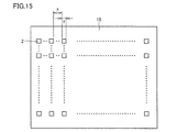
- FIGS. 14 to 17 are schematic plan views showing examples of the mask 15 used when pattern etching is performed on the porous layer 2 formed on the first substrate 1.
- the porous layer 2 has a pattern in which regions covering the porous layer 2 are arranged in a lattice pattern. Therefore, when etching is performed after the mask 15 shown in FIG. 14 is formed on the porous layer 2, the porous layer 2 remains in a lattice pattern on the upper surface of the first substrate 1.
- the removal area ratio is 88%. It becomes. Further, in the mask 15 shown in FIG. 14
- the removal area ratio is 51%. In either case, the removal area ratio was calculated assuming that the size of the upper surface of the porous layer 2 was 10 mm wide ⁇ 10 mm long.
- the mask 15 shown in FIG. 15 has a structure in which regions exposing the porous layer 2 are arranged in a lattice pattern. Therefore, when etching is performed after the mask 15 shown in FIG. 15 is formed on the porous layer 2, through holes that expose the upper surface of the first substrate 1 are formed in a lattice pattern in the porous layer 2. It becomes.
- the removal area ratio is 81%. Also in this case, the removal area ratio was calculated with the size of the upper surface of the porous layer 2 being 10 mm wide ⁇ 10 mm long.
- the planar shape of the region covering the porous layer 2 is not limited to a rectangle, but may be a polygon or a circle as shown in FIG. 16.
- the removal area ratio is 50%. Also in this case, the removal area ratio was calculated with the size of the upper surface of the porous layer 2 being 10 mm wide ⁇ 10 mm long.
- the arrangement form of the region covering the porous layer 2 is not limited to the lattice shape.
- the region covering the porous layer 2 may be arranged, for example, at intervals in the length direction of the porous layer 2, or at intervals in the width direction of the porous layer 2 as shown in FIG. It may be arranged.
- the interval x adjacent to the region covering the porous layer 2 is set to 5 ⁇ m, and the region covering the porous layer 2 is arranged in the side constituting the region covering the porous layer 2 (
- the removal area ratio is 75%. Also in this case, the removal area ratio was calculated with the size of the upper surface of the porous layer 2 being 10 mm wide ⁇ 10 mm long.
- region which exposes the porous layer 2 is not limited to a rectangle, A polygon may be sufficient and a circle may be sufficient.
- the arrangement form of the region exposing the porous layer 2 is not limited to the lattice shape. The region where the porous layer 2 is exposed may be arranged with an interval in the length direction of the porous layer 2, or may be arranged with an interval in the width direction of the porous layer 2.
- a buffer layer 600 is formed on the porous layer 2 and the first substrate 1.
- the buffer layer 600 can be formed by, for example, the MOCVD (Metal Organic Chemical Vapor Deposition) method.
- the material constituting the buffer layer 600 is not particularly limited, but at least one selected from GaN, InGaN, AlGaN, and InN can be used.
- the thickness of the buffer layer 600 can be, for example, 30 nm or more and 50 nm or less.
- an i-type nitride semiconductor layer 500 is formed on the buffer layer 600.
- the i-type nitride semiconductor layer 500 can be formed on the buffer layer 600 by, for example, the MOCVD method.
- the i-type nitride semiconductor layer 500 is, for example, a nitride semiconductor crystal represented by the formula of Al x1 In y1 Gaz1 N (0 ⁇ x1 ⁇ 1, 0 ⁇ y1 ⁇ 1, 0 ⁇ z1 ⁇ 1, x1 + y1 + z1 ⁇ 0). It is preferable to contain.
- the i-type nitride semiconductor layer 500 preferably has an MQW (multiple quantum well) structure or an SQW (single quantum well) structure of a nitride semiconductor crystal.
- the thickness of the i-type nitride semiconductor layer 500 is preferably 20 nm or more and 400 nm or less. When the thickness of the i-type nitride semiconductor layer 500 is 20 nm or more, the i-type nitride semiconductor layer 500 can sufficiently absorb light such as sunlight and generate photocarriers sufficiently. When the thickness of the i-type nitride semiconductor layer 500 is 400 nm or less, the i-type nitride semiconductor layer 500 does not become too thick, so that an n-type nitride semiconductor layer and a p-type nitride semiconductor layer described later are used. The formed internal electric field tends to be sufficiently applied to the i-type nitride semiconductor layer 500.
- a more specific example of the i-type nitride semiconductor layer 500 is, for example, a non-doped In 0.1 Ga 0.9 N film having a thickness of 45 nm.
- the non-doped In 0.1 Ga 0.9 N film is formed, for example, by supplying 10 ⁇ mol of TMG (trimethylgallium), 54 ⁇ mol of TMI (trimethylindium), and 420 mmol of NH 3 (ammonia) to the reactor of the MOCVD apparatus. .
- the i-type nitride semiconductor layer 500 include, for example, a quantum well layer made of 3.5 nm thick In 0.2 Ga 0.8 N and a 6 nm thick GaN layer on the buffer layer 600.
- the i-type nitride semiconductor layer 500 may have a buffer layer for relaxing lattice mismatch with an n-type nitride semiconductor layer described later.
- a buffer layer for example, a quantum well layer made of In s Ga 1-s N (s ⁇ 0.1) having a thickness of less than 2 nm and a barrier layer made of GaN having a thickness of less than 2 nm are alternately stacked.
- An MQW structure is used.
- an n-type nitride semiconductor layer 400 is formed on the i-type nitride semiconductor layer 500.
- N-type nitride semiconductor layer 400 can be formed on i-type nitride semiconductor layer 500 by, for example, MOCVD.
- the n-type nitride semiconductor layer 400 is, for example, a nitride semiconductor represented by the formula of Al x2 In y2 Ga z2 N (0 ⁇ x2 ⁇ 1, 0 ⁇ y2 ⁇ 1, 0 ⁇ z2 ⁇ 1, x2 + y2 + z2 ⁇ 0).
- a crystal doped with an n-type impurity can be used. Examples of the n-type impurity include Si, P, As, or Sb.
- the n-type nitride semiconductor layer 400 and the i-type nitride semiconductor layer 500 may use nitride semiconductor crystals having the same composition or may use nitride semiconductor crystals having different compositions.
- n-type nitride semiconductor layer 400 it is particularly preferable to use an n-type GaN layer in which Si is doped into a GaN crystal.
- the n-type nitride semiconductor layer 400 preferably has a larger band gap energy than the i-type nitride semiconductor layer 500. In this case, a decrease in the light intensity absorbed by the n-type nitride semiconductor layer 400 can be minimized, and the light intensity of light incident on the i-type nitride semiconductor layer 500 is increased. There is a tendency to generate photo carriers.
- the n-type impurity concentration in the n-type nitride semiconductor layer 400 is not particularly limited, but is preferably 1 ⁇ 10 18 / cm 3 or more and 1 ⁇ 10 20 / cm 3 or less.
- the conductivity of n-type nitride semiconductor layer 400 can be increased, and the crystallinity of i-type nitride semiconductor layer 500 is improved without the surface of n-type nitride semiconductor layer 400 being roughened. Tend to be able to.
- a metal layer 300 is formed on the n-type nitride semiconductor layer 400.
- Metal layer 300 can be formed on n-type nitride semiconductor layer 400 by, for example, sputtering or plating.
- the metal layer 300 includes not only the upper surface of the n-type nitride semiconductor layer 400 but also the n-type nitride semiconductor layer 400, the i-type nitride semiconductor layer 500, the buffer layer 600, and the porous layer. It is also formed on each side surface of the second substrate 1 and the first substrate 1.
- a specific example of such a metal layer 300 includes a structure in which a Ni layer having a thickness of 40 nm, a Pt layer and an Au layer having a thickness of 200 nm, and an Ag layer having a thickness of 80 nm are stacked in this order.
- the first substrate 1 is removed using a cutting tool 4.
- the removal of the first substrate 1 can be performed, for example, by pressing the cutting tool 4 near the interface between the first substrate 1 and the porous layer 2 and cutting the vicinity of the interface with the cutting tool 4.
- the cutting tool 4 for example, a cutting tool made of tungsten carbide or the like can be used.
- the porous layer 2 preferably has a Knoop hardness lower than that of the buffer layer 600, and the cutting tool 4 preferably has a Knoop hardness higher than that of the buffer layer 600 and the porous layer 2. In this case, since the porous layer 2 can be easily scraped off with the cutting tool 4, it tends to be easily removed by peeling off the first substrate 1.
- the Knoop hardness of GaN, GaAs, AlGaAs and sapphire are 850 kg / mm 2 , 730 kg / mm 2 , 430 to 520 kg / mm 2 and 1500 to 1800 kg / mm 2 , respectively.
- the Knoop hardness of the SOG film depends on the hole density and is 400 kg / mm 2 or less. Therefore, for example, when the first substrate 1 is made of sapphire, the porous layer 2 is an SOG film, and the buffer layer 600 is made of GaN or AlGaAs, the interface between the first substrate 1 and the porous layer 2 is used.
- the porous layer 2 can be scraped off by pressing a cutting tool 4 made of tungsten carbide in the vicinity.
- the porous layer 2 can be cut into a size of 5 mm wide by 5 mm long using a cutting tool having a width of 5 mm with a SAICAS (surface and interface cutting machine) manufactured by Daipura Wintes. .
- a wider cutting tool is used, the porous layer 2 having a width of 5 mm or more can be scraped off.
- the measuring method of the Knoop hardness is not particularly limited, but the Knoop hardness can be measured using, for example, a Knoop hardness tester.
- Second substrate 200 is attached to the metal layer 300.
- Second substrate 200 can be attached to metal layer 300 using, for example, silver paste.
- the material of the second substrate 200 is not particularly limited, but may be, for example, an alumina-based or titanium oxide-based ceramic, or mica that is lighter than the ceramic.
- a flexible substrate such as a heat resistant resin is preferably used as the second substrate 200. If the second substrate 200 is a flexible substrate such as a heat resistant resin, a flexible photoelectric conversion element can be manufactured.
- a step of forming a metal film containing Ag on a surface (the lower surface of the second substrate 200 in FIG. 8) located on the opposite side of the surface of the second substrate 200 to the surface on which the metal layer 300 is attached. It is preferable to include.
- a metal film containing Ag can be used as a protective film for the second substrate 200 when the buffer layer 600 is removed with aqua regia in a process described later.
- an Ag film is formed on the surface of the second substrate 200
- an AgCl protective film is formed on the surface of the Ag film by aqua regia, so that the second substrate 200 may be left without being removed. It tends to be possible.
- the metal film may be used as a wiring connection portion. it can.
- the buffer layer 600 is removed.
- the buffer layer 600 can be removed by aqua regia or plasma etching, for example.
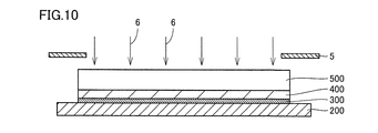
- a p-type nitride semiconductor layer 502 is formed on the i-type nitride semiconductor layer 500.
- ions 6 of p-type impurities are ion-implanted into the i-type nitride semiconductor layer 500 using the mask 5 having a pattern for masking the peripheral region of the i-type nitride semiconductor layer 500 as an ion implantation mask.
- i-type nitride semiconductor layer 500 is annealed. As a result, for example, as shown in FIG.
- p-type nitride semiconductor layer 502 can be formed on the surface portion of i-type nitride semiconductor layer 500 in a region other than the peripheral region. Since the p-type nitride semiconductor layer 502 is formed on the surface portion of the i-type nitride semiconductor layer 500 in a region other than the peripheral region, current leakage at the end surface portion of the photoelectric conversion element can be avoided.
- the surface portion of the i-type nitride semiconductor layer 500 means a side opposite to the surface side of the i-type nitride semiconductor layer 500 on which the n-type nitride semiconductor layer 400 is formed.
- the acceleration energy of the p-type impurity ions 6 can be set to, for example, 30 keV.
- the p-type impurity concentration in the p-type nitride semiconductor layer 502 is not particularly limited, but is preferably set to, for example, 1 ⁇ 10 17 / cm 3 or more and 2 ⁇ 10 19 / cm 3 or less.
- the annealing of the i-type nitride semiconductor layer 500 is preferably performed for 5 minutes in a nitrogen atmosphere at 800 ° C., for example.
- magnesium ions as p-type impurity ions 6 are implanted into the surface portion of the i-type nitride semiconductor layer 500 other than the peripheral region with an acceleration energy of about 30 keV, in a nitrogen atmosphere. Annealing is performed at 800 ° C. for 5 minutes. Thereby, the p-type nitride semiconductor layer 502 having a magnesium concentration of p-type impurities of about 1 ⁇ 10 19 pieces / cm 3 can be formed.
- Transparent electrode layer 700 is formed on the p-type nitride semiconductor layer 502.
- Transparent electrode layer 700 can be formed on p-type nitride semiconductor layer 502 by, for example, magnetron sputtering or ion plating.
- the material of the transparent electrode layer 700 is not particularly limited, but it is preferable to use a single-layer or multi-layer stack made of an oxide of at least one metal selected from the group consisting of zinc, indium, tin and magnesium. .
- the transparent electrode layer 700 include zinc oxide doped with 2% aluminum having a thickness of 320 nm.
- a current collecting electrode may be formed on the transparent electrode layer 700.
- the collector electrode for example, a comb-shaped collector electrode made of at least one selected from the group consisting of nickel, platinum, gold and silver can be formed.
- the large-area photoelectric conversion element 100 of the embodiment which is an example of the photoelectric conversion element of the present invention can be manufactured.
- the photoelectric conversion element 100 manufactured as described above was provided on the second substrate 200, the metal layer 300 provided on the second substrate 200, and the metal layer 300.
- the p-type nitride semiconductor layer 502 and the transparent electrode layer 700 provided on the p-type nitride semiconductor layer 502 are provided.
- FIG. 12 is a schematic cross-sectional view showing the configuration of the photoelectric conversion element 100 of the embodiment.
- the photoelectric conversion element 100 In the photoelectric conversion element 100, light that enters from the transparent electrode layer 700 side, passes through the transparent electrode layer 700 and the p-type nitride semiconductor layer 502, and reaches the i-type nitride semiconductor layer 500 is used as a light absorption layer.
- the i-type nitride semiconductor layer 500 is absorbed.
- the carriers generated in the i-type nitride semiconductor layer 500 can be taken out of the photoelectric conversion element 100 from the metal layer 300 and the transparent electrode layer 700.
- the metal layer 300 can function as a reflective layer that reflects light transmitted through the n-type nitride semiconductor layer 400 toward the i-type nitride semiconductor layer 500.
- the photoelectric conversion element module 101 can be manufactured by electrically connecting a plurality of large-area photoelectric conversion elements 100 manufactured as described above.
- FIG. 13 is a schematic cross-sectional view illustrating a configuration of the photoelectric conversion element module 101 according to the embodiment.
- a photoelectric conversion element module 101 illustrated in FIG. 13 includes a frame 10 provided with a back plate 11, a plurality of photoelectric conversion elements 100 arranged in an array in the frame 10, and the photoelectric conversion elements 100 in electrical series. Or the wiring 12 connected in parallel is provided.
- the frame 10 includes a sealing material 13 and a protective material 14 for protecting the photoelectric conversion element 100 and the wiring 12 from the external environment and external impact.
- serial number and the parallel number of the photoelectric conversion elements 100 in the photoelectric conversion element module 101 can be determined according to the rated voltage and the rated current of the photoelectric conversion element module 101.
- planar shape of the frame body 10 is not particularly limited, and may be a polygonal shape, a circular shape, an elliptical shape, or the like other than the quadrangle shown in FIG.
- the photoelectric conversion element module 101 can be configured to be lightened by mounting the photoelectric conversion element 100 on a curved surface of a vehicle body or the like. .
- the removal of the first substrate 1 having a large area used for the growth of the i-type nitride semiconductor layer 500 and the n-type nitride semiconductor layer 400 is conventionally performed.
- the cutting tool 4 is used instead of the laser beam irradiation and the substrate temperature change as described above. Therefore, even when a large-area substrate is used as the first substrate 1, the removal of the first substrate 1 can be performed more easily and at a lower cost than in the past. Therefore, the photoelectric conversion element 100 having a large area and the photoelectric conversion element module 101 using the photoelectric conversion element 100 can be manufactured at low cost.
- the porous layer 2 is provided on the first substrate 1, so that the porous layer 2 can be easily scraped with the cutting tool 4. Can do. That is, by providing the porous layer 2 on the first substrate 1, the removal by peeling off the first substrate 1 is facilitated. Therefore, even when a large-area substrate is used as the first substrate 1, the removal of the first substrate 1 can be performed more easily and at a lower cost than in the past. Therefore, the photoelectric conversion element 100 having a large area and the photoelectric conversion element module 101 using the photoelectric conversion element 100 can be manufactured at low cost. This effect becomes remarkable when each Knoop hardness of the porous layer 2 and the buffer layer 600 is lower than the Knoop hardness of the cutting tool 4.
- the distance between the region covering the porous layer 2 or the region exposing the porous layer 2 is 5 ⁇ m or more and 30 ⁇ m or less.
- the removal area ratio is preferably 50% or more and 90% or less.
- the first substrate 1 is not an expensive nitride semiconductor substrate but a reusable and relatively inexpensive sapphire substrate, a large-area photoelectric conversion element 100 can be manufactured at a lower cost. can do.
- the photoelectric conversion element 100 of the embodiment uses the i-type nitride semiconductor layer 500 made of a nitride semiconductor crystal as the light absorption layer, the light absorption rate is very high compared to Si and the like.
- the conversion element 100 can be formed thinner than before. Therefore, the degree of freedom in selecting the second substrate 200 is improved, and the flexible and lightweight photoelectric conversion element 100 and photoelectric conversion element module 101 can be formed.
Landscapes
- Chemical & Material Sciences (AREA)
- Engineering & Computer Science (AREA)
- Nanotechnology (AREA)
- Physics & Mathematics (AREA)
- Life Sciences & Earth Sciences (AREA)
- Biophysics (AREA)
- Optics & Photonics (AREA)
- Crystallography & Structural Chemistry (AREA)
- Photovoltaic Devices (AREA)
Abstract
第1の基板(1)上に多孔質層(2)を形成してから、パターンエッチングによって多孔質層(2)の一部を除去する。多孔質層(2)上および第1の基板(1)上に、バッファ層(600)、i型窒化物半導体層(500)、n型窒化物半導体層(400)および金属層(300)を形成してから、切削工具(4)を用いて第1の基板(1)をバッファ層(600)から除去する。
Description
本発明は、光電変換素子の製造方法、光電変換素子および光電変換素子モジュールに関する。
シリコン系材料からなる光電変換素子のバンドギャップエネルギーは、1.1~1.8eVである。そのため、シリコン系材料からなる光電変換素子には、エネルギーの高い0.5μm以下の短波長領域の光に対して感度が小さく、よって、太陽光スペクトルの全ての波長領域を有効に活用できないという材料固有の課題が存在していた。
一方、AlxInyGa(1-x-y)N(0≦x≦1、0≦y≦1、0<x+y≦1)で表される窒化物半導体のバンドギャップエネルギーは、組成比xおよびyに対応して、0.7eV~6.0eVという極めて広い範囲で変化する。このような窒化物半導体は、発光ダイオード(LED)およびレーザーダイオード(LD)などの発光素子用の材料として開発が盛んに行われてきた。上記の組成を有する窒化物半導体を光電変換素子に用いた場合には、0.5μm以下の短波長領域の光に対しても感度を持たせることができるようになる。そのため、このような窒化物半導体は、光電変換素子用の次世代の材料として大変注目されている。
窒化物半導体を用いた従来の光電変換素子は、光の入射側から、p型不純物がドープされたGaN層の下に、AlxInyGa(1-x-y)N(0≦x≦1、0≦y≦1、0<x+y≦1)の式で表わされる、InGaN、AlGaNまたはAlInGaNなどからなるi型窒化物半導体層(光吸収層として機能)とn型不純物がドープされたGaN層とが設けられた構成を有している。
たとえば特許文献1(特開2003-318434号公報)には、次に示す方法にしたがって製造された光電変換素子が開示されている。図18の模式的断面図に示すように、サファイア基板1000の[0001]面上に、窒化物半導体バッファ層(図示せず)、p型窒化物半導体層6000、i型窒化物半導体層5000およびn型窒化物半導体層4000をこの順序で積層する。素子分離を行ない、保護膜8000を形成した後、n型窒化物半導体層4000上にパッド電極3000および支持基板2000を形成する。サファイア基板1000側からエキシマレーザー光60を照射して、サファイア基板1000を除去する。
特許文献1には、次に示すことも開示されている。特許文献1に記載の光電変換素子では、n型窒化物半導体層からp型窒化物半導体層に向かう積層方向を[000-1]方向と一致させることにより、格子定数の違いから生ずる圧電電界が、p-i界面近傍において光を吸収して発生した電子-正孔対の分離を促進し且つn-i界面近傍において伝導帯のヘテロ障壁を低くする方向に、発生する。よって、特許文献1に記載の光電変換素子は高い変換効率を発現する。
しかしながら、このような光電変換素子については、大面積のものを製造することが困難である。そのため、比較的小面積の光電変換素子を多数実装して太陽電池モジュールなどの光電変換素子モジュールを製造する必要があった。
また、たとえば特許文献2(特許第4672753号(特開2009-7241号公報))には、サファイア基板上に窒化物半導体層を積層した後にサファイア基板の温度を常温に戻すことによって、窒化物半導体層をサファイア基板から自然に剥離させる技術が開示されている。
さらに、たとえば特許文献3(特許第4599442号(特開2010-56210号公報))には、窒化物半導体層をサファイア基板から剥離させる別の技術が開示されている。具体的には、サファイア基板上に、AlNからなる第1のバッファ層、AlxGa1-xN(0.8≦s<1)からなる第2のバッファ層、GaN層またはAlGaInN層からなる半導体層およびp型半導体層をこの順に形成する。その後、GaNの禁制帯幅に相当するエネルギーを有する波長よりも波長が短いレーザー光を照射する。
しかしながら、特許文献2および特許文献3に記載のいずれの技術も、太陽電池モジュールなどの光電変換素子モジュールに必要な大面積の光電変換素子の製造に適用できない。
上記の事情に鑑みて、本発明の目的は、窒化物半導体を用いた大面積の光電変換素子を低コストで製造することが可能な光電変換素子の製造方法、光電変換素子および光電変換素子モジュールを提供することにある。
本発明の光電変換素子の製造方法は、第1の基板上に多孔質層を形成する工程と、パターンエッチングによって多孔質層の一部を除去する工程と、多孔質層上および第1の基板上にバッファ層を形成する工程と、バッファ層上にi型窒化物半導体層を形成する工程と、i型窒化物半導体層上にn型窒化物半導体層を形成する工程と、n型窒化物半導体層上に金属層を形成する工程と、切削工具を用いて第1の基板をバッファ層から除去する工程と、金属層に第2の基板を貼り付ける工程と、バッファ層を除去する工程と、バッファ層の除去後にi型窒化物半導体層の表面部にp型窒化物半導体層を形成する工程とを含む。
第1の基板を除去する工程は、第1の基板と多孔質層との界面近傍を切削工具で切削する工程を含むことが好ましい。
切削工具は、多孔質層およびバッファ層よりもヌープ硬度が高い材料で構成されていることが好ましい。
パターンエッチングで使用されるマスクには、多孔質層を覆う領域または多孔質層を露出する領域が間隔をあけて配置されてなるパターンが形成されていることが好ましい。マスクにおいて多孔質層を覆う領域または多孔質層を露出する領域が隣り合う間隔は、5μm以上30μm以下であることが好ましい。マスクから露出する多孔質層の上面の面積の合計は、多孔質層の上面の全面積に対して50%以上90%以下であることが好ましい。
バッファ層は、GaN、InGaN、AlGaN、およびInNの少なくとも1つを含むことが好ましい。
p型窒化物半導体層を形成する工程は、i型窒化物半導体層の表面部であって周縁領域以外の領域にp型不純物イオンを注入する工程を含むことが好ましい。
i型窒化物半導体層はAlx1Iny1Gaz1N(0≦x1≦1、0≦y1≦1、0≦z1≦1、x1+y1+z1≠0)の式で表わされる窒化物半導体結晶を含むことが好ましく、n型窒化物半導体層はAlx2Iny2Gaz2N(0≦x2≦1、0≦y2≦1、0≦z2≦1、x2+y2+z2≠0)の式で表わされる窒化物半導体結晶を含むことが好ましい。
第2の基板の表面のうち金属層が設けられた表面とは反対側の表面にAgを含む金属膜を形成する工程をさらに含むことが好ましい。
本発明の光電変換素子は、本発明の光電変換素子の製造方法により製造され、第2の基板上に設けられた金属層と、金属層上に設けられたn型窒化物半導体層と、n型窒化物半導体層上に設けられたi型窒化物半導体層と、i型窒化物半導体層の表面部であって周縁領域以外の領域に設けられたp型窒化物半導体層とを備える。
第2の基板は、可撓性を有することが好ましい。
本発明の光電変換素子モジュールは、本発明の光電変換素子を含む。
本発明の光電変換素子モジュールは、本発明の光電変換素子を含む。
本発明によれば、窒化物半導体を用いた大面積の光電変換素子を低コストで製造することが可能な光電変換素子の製造方法、光電変換素子および光電変換素子モジュールを提供することができる。
以下、図面を用いて、本発明の光電変換素子の製造方法の一例である実施の形態の光電変換素子の製造方法、本発明の光電変換素子の一例である実施の形態の光電変換素子の構成、および本発明の光電変換素子モジュールの一例である実施の形態の光電変換素子モジュールの構成について説明する。なお、本発明の図面において、同一の参照符号は、同一部分または相当部分を表すものである。また、長さ、幅、厚さ、深さなどの寸法関係は図面の明瞭化と簡略化のために適宜変更されており、実際の寸法関係を表すものではない。
図1~図11は、実施の形態の光電変換素子の製造方法を工程順に示す模式的な断面図である。まず、図1に示すように、第1の基板1上に多孔質層2を形成する。その後、図2に示すように、パターンエッチングにより多孔質層2の一部を除去する。なお、大面積の第1の基板1としては、たとえば、幅10mm×長さ10mm以上の面積を有する基板を挙げることができる。
第1の基板1の材料は、特に限定されないが、低コストで光電変換素子を製造する観点からは、GaAsまたはサファイアを用いることが好ましい。
多孔質層2の構成は、特に限定されない。多孔質層2は、たとえばSOG(Sipn on Glass)膜(膜厚がたとえば1~2μmである)であることが好ましい。
本明細書において、「パターンエッチング」とは、一部を除去したい膜(本実施の形態では多孔質層2)の上面にマスク(このマスクは所定のパターンを有する)を形成した後、マスクから露出する膜の部分をエッチングにより除去することを意味する。マスクの形成方法としては、特に限定されず、フォトレジストを塗布してパターンを露光するという方法を挙げることができる。また、エッチングの手法としては、特に限定されず、ウエットエッチングまたはドライエッチングを選択することができる。
パターンエッチングで使用されるマスクの構成は特に限定されないが、マスクは多孔質層2を覆う領域または多孔質層2を露出する領域が間隔をあけて配置されてなるパターンを有していることが好ましい。多孔質層2を覆う領域または多孔質層2を露出する領域は、マスクにおいて、格子状に配置されていても良いし、幅方向または長さ方向に間隔をあけて配置されていても良い。多孔質層2を覆う領域または多孔質層2を露出する領域の平面形状は特に限定されず、矩形などの多角形であっても良いし、円形であっても良い。
多孔質層2を覆う領域または多孔質層2を露出する領域が隣り合う間隔は、5μm以上30μm以下であることが好ましく、より好ましくは6μm以上20μm以下である。多孔質層2を覆う領域または多孔質層2を露出する領域の隣り合う間隔が5μm未満であれば、パターンの形成が困難となる場合がある。一方、多孔質層2を覆う領域または多孔質層2を露出する領域の隣り合う間隔が30μmを超えると、第1の基板1と多孔質層2との界面に切削工具4を挿入することが困難となることが予想され、そのため、加工不良の発生を招くことがある。
除去面積比(除去面積比とは、多孔質層2の上面の全面積に対する、マスクから露出する多孔質層2の上面の合計面積の割合である。)は50%以上90%以下であることが好ましく、より好ましくは55%以上85%以下である。除去面積比が50%未満であれば、多孔質層2を除去し損なうことがあり、そのため、多孔質層2の削り残しが発生するなどの理由から加工不良の発生を招くことがある。一方、除去面積比が90%を超えると、多孔質層2が除去される部分が多くなるため、図7に示す工程において第1の基板1の剥離による除去が難しくなることがある。以下では、図14~図17を用いてマスクの具体的な構成を示す。図14~図17は、それぞれ、第1の基板1上に形成された多孔質層2をパターエッチングするときに使用されるマスク15の一例を示す模式的な平面図である。
図14に示すマスク15は、多孔質層2を覆う領域が格子状に配置されてなるパターンを有する。そのため、図14に示すマスク15を多孔質層2上に形成してからエッチングを行なうと、多孔質層2は第1の基板1の上面において格子状に残存することとなる。図14に示すマスク15において、多孔質層2を覆う領域の隣り合う間隔xを0.3μmとし、多孔質層2を覆う領域の一辺yを4.7μmとした場合、除去面積比は88%となる。また、図14に示すマスク15において、多孔質層2を覆う領域の隣り合う間隔xを8.5μmとし、多孔質層2を覆う領域の一辺yを21.5μmとした場合、除去面積比は51%となる。なお、どちらの場合においても、多孔質層2の上面の大きさを幅10mm×長さ10mmとして除去面積比を算出した。
図15に示すマスク15は、多孔質層2を露出する領域が格子状に配置されて構成されている。そのため、図15に示すマスク15を多孔質層2上に形成してからエッチングを行なうと、多孔質層2には第1の基板1の上面を露出する貫通孔が格子状に形成されることとなる。図15に示すマスク15において、多孔質層2を露出する領域が隣り合う間隔xを5.4μmとし、多孔質層2を露出する領域の一辺yを0.6μmとした場合、除去面積比は81%となる。なお、この場合においても、多孔質層2の上面の大きさを幅10mm×長さ10mmとして除去面積比を算出した。
図14に示すマスク15において、多孔質層2を覆う領域の平面形状は矩形に限定されず、多角形であっても良いし、図16に示すように円形であっても良い。図16に示すマスク15において、多孔質層2を覆う領域の隣り合う間隔xを5μmとし、多孔質層2を覆う領域の直径φを20μmとした場合、除去面積比は50%となる。なお、この場合においても、多孔質層2の上面の大きさを幅10mm×長さ10mmとして除去面積比を算出した。
図14に示すマスク15において、多孔質層2を覆う領域の配置形態は格子状に限定されない。多孔質層2を覆う領域は、たとえば、多孔質層2の長さ方向に間隔をあけて配置されていても良いし、図17に示すように多孔質層2の幅方向に間隔をあけて配置されていても良い。図17に示すマスク15において、多孔質層2を覆う領域の隣り合う間隔xを5μmとし、多孔質層2を覆う領域を構成する辺のうち多孔質層2を覆う領域が配置される方向(図17の横方向)における辺の長さyを15μmとした場合、除去面積比は75%となる。なお、この場合においても、多孔質層2の上面の大きさを幅10mm×長さ10mmとして除去面積比を算出した。
なお、図15に示すマスク15においても、多孔質層2を露出する領域の平面形状は矩形に限定されず、多角形であっても良いし、円形であっても良い。また、図15に示すマスク15においても、多孔質層2を露出する領域の配置形態は格子状に限定されない。多孔質層2を露出する領域は、多孔質層2の長さ方向に間隔をあけて配置されていても良いし、多孔質層2の幅方向に間隔をあけて配置されていても良い。
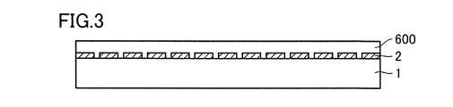
次に、図3に示すように、多孔質層2上および第1の基板1上にバッファ層600を形成する。バッファ層600は、たとえばMOCVD(Metal Organic Chemical Vapor Deposition)法によって形成することができる。
バッファ層600を構成する材料としては、特に限定されないが、GaN、InGaN、AlGaN、およびInNから選択される少なくとも1種類を用いることができる。また、バッファ層600の厚さは、たとえば、30nm以上50nm以下とすることができる。
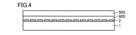
次に、図4に示すように、バッファ層600上にi型窒化物半導体層500を形成する。i型窒化物半導体層500は、たとえばMOCVD法によって、バッファ層600上に形成することができる。
i型窒化物半導体層500は、たとえば、Alx1Iny1Gaz1N(0≦x1≦1、0≦y1≦1、0≦z1≦1、x1+y1+z1≠0)の式で表わされる窒化物半導体結晶を含むことが好ましい。i型窒化物半導体層500は、窒化物半導体結晶のMQW(多重量子井戸)構造またはSQW(単一量子井戸)構造を有していることが好ましい。
i型窒化物半導体層500の厚さは、20nm以上400nm以下であることが好ましい。i型窒化物半導体層500の厚さが20nm以上である場合には、i型窒化物半導体層500が太陽光などの光を十分に吸収してフォトキャリアを十分に発生させることができる。i型窒化物半導体層500の厚さが400nm以下である場合には、i型窒化物半導体層500が厚くなりすぎないため、後述するn型窒化物半導体層とp型窒化物半導体層とによって形成される内部電界がi型窒化物半導体層500に十分に印加される傾向にある。
i型窒化物半導体層500のより具体的な例としては、たとえば、厚さ45nmのノンドープのIn0.1Ga0.9N膜が挙げられる。ノンドープのIn0.1Ga0.9N膜は、たとえば、MOCVD装置の反応炉に、TMG(トリメチルガリウム)を10μmol、TMI(トリメチルインジウム)を54μmolおよびNH3(アンモニア)を420mmol供給することによって、形成される。
i型窒化物半導体層500のより具体的な他の例としては、たとえば、バッファ層600上に、厚さ3.5nmのIn0.2Ga0.8Nからなる量子井戸層と、厚さ6nmのGaNからなる障壁層とが交互に6層積層されたMQW構造が挙げられる。なお、この場合に量子井戸層と障壁層との交互積層数が6層に限定されないことは言うまでもない。
また、i型窒化物半導体層500は、後述するn型窒化物半導体層との格子不整合を緩和するための緩衝層を有していてもよい。緩衝層としては、たとえば、厚さ2nm未満のInsGa1-sN(s<0.1)からなる量子井戸層と、厚さ2nm未満のGaNからなる障壁層とが交互に20層積層されたMQW構造が挙げられる。
次に、図5に示すように、i型窒化物半導体層500上にn型窒化物半導体層400を形成する。n型窒化物半導体層400は、たとえばMOCVD法によって、i型窒化物半導体層500上に形成することができる。
n型窒化物半導体層400としては、たとえば、Alx2Iny2Gaz2N(0≦x2≦1、0≦y2≦1、0≦z2≦1、x2+y2+z2≠0)の式で表わされる窒化物半導体結晶にn型不純物をドープしたものを用いることができる。n型不純物としては、たとえば、Si、P、AsまたはSbなどが挙げられる。なお、n型窒化物半導体層400とi型窒化物半導体層500とは同一の組成の窒化物半導体結晶を用いてもよく、異なる組成の窒化物半導体結晶を用いてもよい。
n型窒化物半導体層400としては、なかでも、SiがGaN結晶にドープされたn型GaN層を用いることが好ましい。
n型窒化物半導体層400は、i型窒化物半導体層500よりも大きなバンドギャップエネルギーを有していることが好ましい。この場合には、n型窒化物半導体層400によって吸収される光強度の減少を最小限にすることができ、i型窒化物半導体層500に入射する光の光強度が大きくなるため、多くのフォトキャリアが発生する傾向にある。
n型窒化物半導体層400におけるn型不純物濃度は、特に限定されないが、1×10¹⁸個/cm3以上1×1020個/cm3以下であることが好ましい。この場合には、n型窒化物半導体層400の導電率を高くすることができるとともに、n型窒化物半導体層400の表面が荒れることなく、i型窒化物半導体層500の結晶性を向上することができる傾向にある。
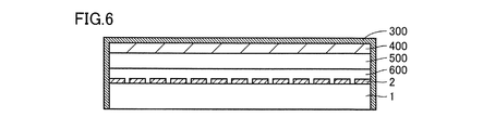
次に、図6に示すように、n型窒化物半導体層400上に金属層300を形成する。金属層300は、たとえばスパッタ法またはメッキ法によって、n型窒化物半導体層400上に形成することができる。なお、本実施の形態においては、金属層300は、n型窒化物半導体層400の上面だけでなく、n型窒化物半導体層400、i型窒化物半導体層500、バッファ層600、多孔質層2および第1の基板1のそれぞれの側面にも形成されている。
このような金属層300の具体的な例としては、厚さ40nmのNi層、厚さ200nmのPt層およびAu層、ならびに厚さ80nmのAg層をこの順序に積層した構成が挙げられる。
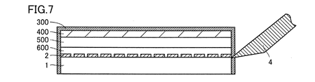
次に、図7に示すように、切削工具4を用いて第1の基板1を除去する。第1の基板1の除去は、たとえば第1の基板1と多孔質層2との界面近傍に切削工具4を押し当てて、当該界面近傍を切削工具4で切削することにより行なうことができる。切削工具4としては、たとえばタングステンカーバイトなどからなる切削工具を用いることができる。
多孔質層2はバッファ層600よりヌープ硬度が低く、切削工具4は、バッファ層600及び多孔質層2よりもヌープ硬度が高いことが好ましい。この場合には、切削工具4で多孔質層2を容易に削り取ることができるため、第1の基板1の剥離による除去が容易となる傾向にある。
GaN、GaAs、AlGaAsおよびサファイアのヌープ硬度は、それぞれ、850kg/mm2、730kg/mm2、430~520kg/mm2および1500~1800kg/mm2である。SOG膜のヌープ硬度は孔の密度に依存し、400kg/mm2以下である。したがって、たとえば、第1の基板1がサファイアからなり、多孔質層2がSOG膜であり、バッファ層600がGaNまたはAlGaAsからなる場合には、第1の基板1と多孔質層2との界面近傍にタングステンカーバイトからなる切削工具4を押し当てて、多孔質層2を削り取ることができる。
より具体的には、ダイプラ・ウィンテス社製SAICAS(表面および界面切削加工装置)で、幅5mmの切削工具を用いて、多孔質層2を幅5mm×長さ5mmの大きさに削り取ることができる。なお、幅のより広い切削工具を用いた場合には、幅5mm以上の多孔質層2を削り取ることができる。
ここで、ヌープ硬度の測定方法は特に限定されないが、たとえばヌープかたさ試験機(Knoop hardness)を用いてヌープ硬度を測定することができる。
次に、図8に示すように、金属層300に第2の基板200を貼り付ける。第2の基板200は、たとえば銀ペーストなどを用いて金属層300に貼り付けることができる。
第2の基板200の材料は、特に限定されないが、たとえば、アルミナ系または酸化チタン系のセラミックであっても良いし、セラミックよりも軽量である雲母であっても良い。なかでも、第2の基板200としては、耐熱性樹脂などの可撓性を有する基板を用いることが好ましい。第2の基板200が耐熱性樹脂などの可撓性を有する基板であれば、可撓性を有する光電変換素子を製造することができる。
第2の基板200の表面のうち金属層300が貼り付けられた面とは反対側に位置する面(図8における第2の基板200の下面)にAgを含む金属膜を形成する工程をさらに含むことが好ましい。この場合には、後述する工程においてバッファ層600を王水で除去する場合に、Agを含む金属膜を第2の基板200の保護膜として用いることができる。たとえば、第2の基板200の表面にAg膜を形成した場合には、王水によってAg膜の表面にAgClの保護膜が形成されるので、第2の基板200を除去せずに残すことができる傾向にある。また、第2の基板200の表面にAgを含む金属膜が形成された場合には、後述するように、光電変換素子をモジュール化する場合に、当該金属膜を配線の接続部とすることができる。
次に、図9に示すように、バッファ層600を除去する。バッファ層600は、たとえば王水またはプラズマエッチングなどによって除去することができる。
次に、図10に示すように、バッファ層600の除去後に、i型窒化物半導体層500にp型窒化物半導体層502を形成する。たとえば、i型窒化物半導体層500の周縁領域をマスクするパターンを有するマスク5をイオン注入マスクとして、p型不純物のイオン6をi型窒化物半導体層500にイオン注入する。その後、i型窒化物半導体層500をアニールする。これにより、たとえば図11に示すように、i型窒化物半導体層500の表面部であって周縁領域以外の領域に、p型窒化物半導体層502を形成することができる。p型窒化物半導体層502がi型窒化物半導体層500の表面部であって周縁領域以外の領域に形成されるので、光電変換素子の端面部での電流リークを回避することができる。ここで、i型窒化物半導体層500の表面部とは、n型窒化物半導体層400が形成されているi型窒化物半導体層500の表面側とは反対側を意味する。
p型不純物のイオン6としては、たとえばマグネシウムのイオンなどを用いることができる。また、p型不純物のイオン6の加速エネルギーは、たとえば30keVとすることができる。また、p型窒化物半導体層502におけるp型不純物濃度は、特に限定されないが、たとえば1×10¹⁷個/cm3以上2×1019個/cm3以下とすることが好ましい。
また、i型窒化物半導体層500のアニールは、たとえば、800℃の窒素雰囲気で、5分間行なうことが好ましい。
より具体的には、i型窒化物半導体層500の表面部であって周縁領域以外の領域に、約30keVの加速エネルギーでp型不純物のイオン6としてのマグネシウムイオンをイオン注入し、窒素雰囲気中、800℃で5分間アニールを行なう。これにより、p型不純物であるマグネシウム濃度が1×10¹⁹個/cm3程度のp型窒化物半導体層502を形成することができる。
次に、図11に示すように、p型窒化物半導体層502上に透明電極層700を形成する。透明電極層700は、たとえばマグネトロンスパッタ法またはイオンプレーティング法によって、p型窒化物半導体層502上に形成することができる。
透明電極層700の材料は、特に限定されないが、亜鉛、インジウム、錫およびマグネシウムからなる群から選択された少なくとも1種の金属の酸化物からなる単層または複数層の積層体を用いることが好ましい。
透明電極層700の具体的な例としては、厚さ320nmの2%のアルミニウムがドープされた酸化亜鉛が挙げられる。
なお、透明電極層700上に集電電極を形成してもよい。集電電極としては、たとえば、ニッケル、白金、金および銀からなる群から選択された少なくとも1種からなる櫛形状の集電電極などを形成することができる。
以上により、本発明の光電変換素子の一例である実施の形態の大面積の光電変換素子100を製造することができる。
このようにして製造された光電変換素子100は、図12に示すように、第2の基板200と、第2の基板200上に設けられた金属層300と、金属層300上に設けられたn型窒化物半導体層400と、n型窒化物半導体層400上に設けられたi型窒化物半導体層500と、i型窒化物半導体層500の表面部であって周縁領域以外の領域に設けられたp型窒化物半導体層502と、p型窒化物半導体層502上に設けられた透明電極層700とを備えている。なお、図12は、実施の形態の光電変換素子100の構成を示す模式的な断面図である。
光電変換素子100においては、透明電極層700側から入射し、透明電極層700およびp型窒化物半導体層502を透過して、i型窒化物半導体層500に到達した光は、光吸収層としてのi型窒化物半導体層500で吸収される。そして、i型窒化物半導体層500で発生したキャリアは、金属層300および透明電極層700から、光電変換素子100の外部に取り出すことができる。なお、金属層300は、n型窒化物半導体層400を透過してきた光をi型窒化物半導体層500側に反射させる反射層として機能させることができる。
たとえば図13に示すように、上記のようにして製造された大面積の光電変換素子100の複数を電気的に接続することによって、光電変換素子モジュール101を製造することができる。図13は、実施の形態の光電変換素子モジュール101の構成を示す模式的な断面図である。
図13に示す光電変換素子モジュール101は、背面板11を備えた枠体10と、枠体10内にアレイ状に配列された複数の光電変換素子100と、光電変換素子100が電気的に直列または並列に接続された配線12と、を備えている。また、枠体10は、光電変換素子100と配線12とを外部環境および外部衝撃から保護するための封止材13および保護材14を備えている。
なお、光電変換素子モジュール101における光電変換素子100の直列数および並列数は、光電変換素子モジュール101の定格電圧および定格電流に応じて定めることができる。
また、枠体10の平面形状は、特に限定されず、たとえば、図13に示す四角形以外にも多角形、円形状または楕円形などの形状であってもよい。
また、第2の基板200の材料に可撓性を有する材料を用いた場合には、車体等の曲面に光電変換素子100を実装して軽量化した光電変換素子モジュール101を構成することができる。
上記の光電変換素子100および光電変換素子モジュール101の製造においては、i型窒化物半導体層500およびn型窒化物半導体層400の成長に用いた大面積の第1の基板1の除去を、従来のようにレーザー光の照射および基板の温度変化によって行なうのではなく、切削工具4を用いて行なっている。そのため、第1の基板1として大面積の基板を用いた場合でも、第1の基板1の除去を従来よりも容易に、かつ低コストで行なうことができる。よって、大面積の光電変換素子100およびそれを用いた光電変換素子モジュール101を低コストで製造することができる。
また、上記の光電変換素子100および光電変換素子モジュール101の製造においては、第1の基板1の上に多孔質層2を設けているので、切削工具4で多孔質層2を容易に削り取ることができる。つまり、第1の基板1の上に多孔質層2を設けることにより、第1の基板1の剥離による除去が容易となる。よって、第1の基板1として大面積の基板を用いた場合でも、第1の基板1の除去を従来よりも容易に、かつ低コストで行なうことができる。したがって、大面積の光電変換素子100およびそれを用いた光電変換素子モジュール101を低コストで製造することができる。この効果は、多孔質層2およびバッファ層600の各ヌープ硬度が切削工具4のヌープ硬度よりも低い場合に、顕著となる。
また、多孔質層2をパターンエッチングにより形成するときに使用されるマスクにおいては、多孔質層2を覆う領域または多孔質層2を露出する領域が隣り合う間隔は5μm以上30μm以下であることが好ましく、除去面積比は50%以上90%以下であることが好ましい。これにより、多孔質層2の形成が容易となり、切削工具4による多孔質層2の削り取りがさらに容易となる。よって、第1の基板1の剥離による除去がさらに容易となる。したがって、第1の基板1として大面積の基板を用いた場合でも、第1の基板1の除去を従来よりもさらに容易且つ低コストで行なうことができる。
また、第1の基板1として、高価な窒化物半導体基板ではなく、再利用可能であって比較的安価なサファイア基板を用いた場合には、大面積の光電変換素子100をさらに低コストで製造することができる。
さらに、実施の形態の光電変換素子100には、光吸収層として、窒化物半導体結晶からなるi型窒化物半導体層500を用いていることから、Si等に比べ光吸収率が非常高く、光電変換素子100を従来よりも薄く形成することができる。そのため、第2の基板200の選択の自由度が向上し、可撓性を有し、かつ軽量の光電変換素子100および光電変換素子モジュール101を形成することができる。
今回開示された実施の形態はすべての点で例示であって制限的なものではないと考えられるべきである。本発明の範囲は上記した説明ではなくて請求の範囲によって示され、請求の範囲と均等の意味および範囲内でのすべての変更が含まれることが意図される。
1 第1の基板、2 多孔質層、4 切削工具、5 マスク、6 p型不純物イオン、10 枠体、11 背面板、12 配線、13 封止材、14 保護材、15 マスク、60 エキシマレーザー光、100 光電変換素子、101 光電変換素子モジュール、200 第2の基板、300 金属層、400,4000 n型窒化物半導体層、500,5000 i型窒化物半導体層、502,6000 p型窒化物半導体層、600 バッファ層、700 透明電極層、1000 サファイア基板、2000 支持基板、3000 パッド電極、8000 保護膜。
Claims (11)
- 第1の基板上に多孔質層を形成する工程と、
パターンエッチングによって前記多孔質層の一部を除去する工程と、
前記多孔質層上および前記第1の基板上にバッファ層を形成する工程と、
前記バッファ層上にi型窒化物半導体層を形成する工程と、
前記i型窒化物半導体層上にn型窒化物半導体層を形成する工程と、
前記n型窒化物半導体層上に金属層を形成する工程と、
切削工具を用いて前記第1の基板を前記バッファ層から除去する工程と、
前記金属層に第2の基板を貼り付ける工程と、
前記バッファ層を除去する工程と、
前記バッファ層の除去後に、前記i型窒化物半導体層の表面部にp型窒化物半導体層を形成する工程と、を含む、光電変換素子の製造方法。 - 前記第1の基板を除去する工程は、前記第1の基板と前記多孔質層との界面近傍を前記切削工具で切削する工程を含む、請求項1に記載の光電変換素子の製造方法。
- 前記切削工具は、前記多孔質層および前記バッファ層よりもヌープ硬度が高い材料で構成されている、請求項2に記載の光電変換素子の製造方法。
- 前記パターンエッチングで使用されるマスクには、前記多孔質層を覆う領域または前記多孔質層を露出させる領域が間隔をあけて配置されてなるパターンが形成されており、
前記マスクにおいて前記多孔質層を覆う領域または前記多孔質層を露出する領域が隣り合う間隔は、5μm以上30μm以下であり、
前記マスクから露出する多孔質層の上面の面積の合計は、前記多孔質層の上面の全面積に対して50%以上90%以下である請求項1~3のいずれかに記載の光電変換素子の製造方法。 - 前記バッファ層は、GaN、InGaN、AlGaN、およびInNの少なくとも1つを含む、請求項1~4のいずれかに記載の光電変換素子の製造方法。
- 前記p型窒化物半導体層を形成する工程は、前記i型窒化物半導体層の前記表面部であって周縁領域以外の領域にp型不純物イオンを注入する工程を含む、請求項1~5のいずれかに記載の光電変換素子の製造方法。
- 前記i型窒化物半導体層は、Alx1Iny1Gaz1N(0≦x1≦1、0≦y1≦1、0≦z1≦1、x1+y1+z1≠0)の式で表わされる窒化物半導体結晶を含み、
前記n型窒化物半導体層は、Alx2Iny2Gaz2N(0≦x2≦1、0≦y2≦1、0≦z2≦1、x2+y2+z2≠0)の式で表わされる窒化物半導体結晶を含む、請求項1~6のいずれかに記載の光電変換素子の製造方法。 - 前記第2の基板の表面のうち前記金属層が貼り付けられた表面とは反対側の表面にAgを含む金属膜を形成する工程をさらに含む、請求項1~7のいずれかに記載の光電変換素子の製造方法。
- 請求項1~8のいずれかに記載の光電変換素子の製造方法により製造された光電変換素子であって、
前記第2の基板上に設けられた金属層と、
前記金属層上に設けられたn型窒化物半導体層と、
前記n型窒化物半導体層上に設けられたi型窒化物半導体層と、
前記i型窒化物半導体層の表面部であって周縁領域以外の領域に設けられたp型窒化物半導体層とを備えた、光電変換素子。 - 前記第2の基板は、可撓性を有する、請求項9に記載の光電変換素子。
- 請求項9または10に記載の光電変換素子を含む、光電変換素子モジュール。
Applications Claiming Priority (2)
| Application Number | Priority Date | Filing Date | Title |
|---|---|---|---|
| JP2012033787A JP2013171904A (ja) | 2012-02-20 | 2012-02-20 | 光電変換素子の製造方法、光電変換素子および光電変換素子モジュール |
| JP2012-033787 | 2012-02-20 |
Publications (1)
| Publication Number | Publication Date |
|---|---|
| WO2013125264A1 true WO2013125264A1 (ja) | 2013-08-29 |
Family
ID=49005458
Family Applications (1)
| Application Number | Title | Priority Date | Filing Date |
|---|---|---|---|
| PCT/JP2013/050729 Ceased WO2013125264A1 (ja) | 2012-02-20 | 2013-01-17 | 光電変換素子の製造方法、光電変換素子および光電変換素子モジュール |
Country Status (2)
| Country | Link |
|---|---|
| JP (1) | JP2013171904A (ja) |
| WO (1) | WO2013125264A1 (ja) |
Citations (5)
| Publication number | Priority date | Publication date | Assignee | Title |
|---|---|---|---|---|
| JPH1012903A (ja) * | 1996-06-26 | 1998-01-16 | Kyocera Corp | 光電変換装置 |
| JP2000036609A (ja) * | 1998-05-15 | 2000-02-02 | Canon Inc | 太陽電池の製造方法と薄膜半導体の製造方法、薄膜半導体の分離方法及び半導体形成方法 |
| JP2003229588A (ja) * | 2002-02-01 | 2003-08-15 | Canon Inc | 薄膜半導体の製造方法及び太陽電池の製造方法 |
| JP2003318434A (ja) * | 2002-04-25 | 2003-11-07 | Nichia Chem Ind Ltd | 窒化物半導体受光素子とその製造方法 |
| JP2010267934A (ja) * | 2009-05-18 | 2010-11-25 | Panasonic Corp | 太陽電池およびその製造方法 |
-
2012
- 2012-02-20 JP JP2012033787A patent/JP2013171904A/ja active Pending
-
2013
- 2013-01-17 WO PCT/JP2013/050729 patent/WO2013125264A1/ja not_active Ceased
Patent Citations (5)
| Publication number | Priority date | Publication date | Assignee | Title |
|---|---|---|---|---|
| JPH1012903A (ja) * | 1996-06-26 | 1998-01-16 | Kyocera Corp | 光電変換装置 |
| JP2000036609A (ja) * | 1998-05-15 | 2000-02-02 | Canon Inc | 太陽電池の製造方法と薄膜半導体の製造方法、薄膜半導体の分離方法及び半導体形成方法 |
| JP2003229588A (ja) * | 2002-02-01 | 2003-08-15 | Canon Inc | 薄膜半導体の製造方法及び太陽電池の製造方法 |
| JP2003318434A (ja) * | 2002-04-25 | 2003-11-07 | Nichia Chem Ind Ltd | 窒化物半導体受光素子とその製造方法 |
| JP2010267934A (ja) * | 2009-05-18 | 2010-11-25 | Panasonic Corp | 太陽電池およびその製造方法 |
Also Published As
| Publication number | Publication date |
|---|---|
| JP2013171904A (ja) | 2013-09-02 |
Similar Documents
| Publication | Publication Date | Title |
|---|---|---|
| JP6917417B2 (ja) | 光電素子及びその製造方法 | |
| KR101894045B1 (ko) | 발광 다이오드 패키지 및 그의 제조 방법 | |
| EP2426743B1 (en) | GaN compound semiconductor light emitting element and method of manufacturing the same | |
| EP2259344B1 (en) | Light emitting device and manufacturing method for same | |
| US8258521B2 (en) | Radiation-emitting semiconductor body with carrier substrate and method for the production thereof | |
| KR102200757B1 (ko) | 향상된 효율을 위해 구성된 낮은 밴드갭 활성층을 가지는 광활성 장치 및 관련 방법 | |
| JP5414010B2 (ja) | 多接合型化合物太陽電池セル、多接合型化合物太陽電池およびその製造方法 | |
| JP2015508941A (ja) | オプトエレクトロニクス半導体チップ | |
| EP3127143A1 (en) | Methods of recycling substrates and carrier substrates | |
| JP2015153826A (ja) | 窒化物半導体発光素子及びその製造方法 | |
| JPWO2017057029A1 (ja) | 薄膜化合物太陽電池、薄膜化合物太陽電池の製造方法、薄膜化合物太陽電池アレイおよび薄膜化合物太陽電池アレイの製造方法 | |
| EP2426741B1 (en) | Method of fabricating a semiconductor light emitting device | |
| US20110147786A1 (en) | Light-emitting device and manufacturing method thereof | |
| KR101619110B1 (ko) | 반도체 광전소자 및 이의 제조방법 | |
| KR20130091501A (ko) | 반도체 발광소자 및 그 제조방법 | |
| KR20120034964A (ko) | 기판, 상기 기판을 포함하는 태양 전지 및 이들의 제조 방법 | |
| WO2013073275A1 (ja) | 光電変換素子の製造方法、光電変換素子および光電変換素子モジュール | |
| KR20150042409A (ko) | 발광 소자의 제조 방법 | |
| KR101383161B1 (ko) | 발광 다이오드 및 그 제조 방법 | |
| JPWO2015140849A1 (ja) | 紫外線発光素子の製造方法、紫外線発光素子 | |
| WO2013125264A1 (ja) | 光電変換素子の製造方法、光電変換素子および光電変換素子モジュール | |
| JP5090543B2 (ja) | 光電変換素子および光電変換素子の製造方法 | |
| US10861991B2 (en) | Compound semiconductor solar cell and method of manufacturing the same | |
| JP2012129438A (ja) | 半導体デバイスの製造方法、エピ成長用積層支持基板およびデバイス用積層支持基板 | |
| JP2011071449A (ja) | 半導体発光素子の製造方法 |
Legal Events
| Date | Code | Title | Description |
|---|---|---|---|
| 121 | Ep: the epo has been informed by wipo that ep was designated in this application |
Ref document number: 13751647 Country of ref document: EP Kind code of ref document: A1 |
|
| NENP | Non-entry into the national phase |
Ref country code: DE |
|
| 122 | Ep: pct application non-entry in european phase |
Ref document number: 13751647 Country of ref document: EP Kind code of ref document: A1 |